Semiconductor Device Modeling and Characterization – EE5342 Lecture 37 – Spring 2011 Professor...
47
Semiconductor Device Modeling and Characterization – EE5342 Lecture 37 – Spring 2011 Professor Ronald L. Carter [email protected] http://www.uta.edu/ronc/
-
Upload
bridget-marshall -
Category
Documents
-
view
226 -
download
6
Transcript of Semiconductor Device Modeling and Characterization – EE5342 Lecture 37 – Spring 2011 Professor...

Semiconductor Device Modeling and
Characterization – EE5342 Lecture 37 – Spring 2011
Professor Ronald L. [email protected]
http://www.uta.edu/ronc/

©rlc L37-04May2011
SPICE mosfet Model Instance CARM*, Ch. 4, p. 290M MOSFET
General Form
M<name> <drain node> <gate node> <source node>+ <bulk/substrate node> <model name>+ [L=<value>] [W=<value>]+ [AD=<value>] [AS=<value>]+ [PD=<value>] [PS=<value>]+ [NRD=<value>] [NRS=<value>]+ [NRG=<value>] [NRB=<value>]+ [M=<value>]
Examples
M1 14 2 13 0 PNOM L=25u W=12uM13 15 3 0 0 PSTRONGM16 17 3 0 0 PSTRONG M=2M28 0 2 100 100 NWEAK L=33u W=12u+ AD=288p AS=288p PD=60u PS=60u NRD=14 NRS=24 NRG=10
L = Ch. L. [m]W = Ch. W. [m]AD = Drain A [m2]AS = Source A[m2]NRD, NRS = D and S diff in squares
M = device multiplier

©rlc L37-04May2011
CARM*, Ch. 4, p. 99Model Forms
.MODEL <model name> NMOS [model parameters]
.MODEL <model name> PMOS [model parameters]
As shown in Figure 11, the MOSFET is modeled as an in tr insic MOSFET with ohmic resistances in series with the drain , source, gate, and bulk (substrate). There is also a shunt resistance (RDS) in parallel with the drain-source channel.
[L=<value>] [W=<value>] cannot be used in conjunction with Monte Carlo analysis .
The simulator provides four MOSFET device models, which differ in the formulation of the I-V characteristic. The LEVEL parameter selects between di fferent models :
LEVEL=1 is the Shichman-Hodges model (see reference [1])LEVEL=2 is a geometry-based, analytic model (see reference [2])LEVEL=3 is a semi-empirical, short-channel model (see reference [2])LEVEL=4 is the BSIM model (see reference [3])LEVEL=5 is the BSIM3 model (see reference [7] Version 1.0)LEVEL=6 is the BSIM3 model (see reference [7] Version 2.0)
L and W are the channel length and width, and are decreased to get the effective channel length and width. L and W can be specified in the device, model, or .OPTIONS statements. The value in the device statement supersedes the va lue in the model sta tement, which supersedes the value in the .OPTIONS statement.

©rlc L37-04May2011
SPICE mosfet model levels• Level 1 is the Schichman-Hodges
model• Level 2 is a geometry-based,
analytical model• Level 3 is a semi-empirical, short-
channel model• Level 4 is the BSIM1 model• Level 5 is the BSIM2 model, etc.

©rlc L37-04May2011
SPICE ParametersLevel 1 - 3 (Static)Par am. Parameter Description Def . Typ. Units
VTO Zero-bias Vthresh 1 1 V
KP Transconductance 2.E-05 3.E-05 A/ V 2̂
GAMMA Body-eff ect par. 0.0 0.35 V 1̂/ 2
PHI Surf ace inversion pot. 0.6 0.65 V
LAMBDA Channel-length mod. 0.0 0.02 1/ V
TOX Thin oxide thickness 1.E-07 1.E-07 m
NSUB Substrate doping 0.0 1.E+15 cm̂ -3
NSS Surf ace state density 0.0 1.E+10 cm̂ -2
LD Lateral diff usion 0.0 8.E-05 m

©rlc L37-04May2011
Par am. Parameter Description Def . Typ. Units
TPG Type of gate material* 1 1
UO Surf ace mobility 600 700 cm̂ 2/ V-s
I S Bulk j ctn. sat. curr. 1.E-14 1.E-15 A
J S Bulk j ctn. sat. curr. dens. A/ m̂ 2
PB Bulk junction potential 0.8 0.75 V
RD Drain ohmic resistance 0 10 Ohms
RS Source ohmic resistance 0 10 Ohms
RSH S/ D sheet ohmic res. 0 10 Ohms/ sq
SPICE ParametersLevel 1 - 3 (Static)
* 0 = aluminum gate, 1 = silicon gate opposite substrate type, 2 = silicon gate same as substrate.

©rlc L37-04May2011
SPICE ParametersLevel 1 - 3 (Q & N)Par am. Parameter Description Def . Typ. Units
CJ Zero-bias bulk cap./ A 0 1.E-09 Fd/ m̂ 2
MJ Bulk j ctn. grading coeff . 0.5 0.5
CJ SW Zero-bias perimeter C/ l 0 1.E-09 Fd/ m
MJ SW Per. C grading coeff . 0.5 0.5
FC For.-bias cap. coeff . 0.5 0.5
CGBO Gate-bulk overlap C/ L 0 2.E-10 Fd/ m
CGDO Gate-drain overlap C/ L 0 4.E-11 Fd/ m
CGSO G-S overlap C/ L 0 4.E-11 Fd/ m
AF Flicker-noise exp. 1 1.2
KF Flicker-noise coeff . 0.0 1.E-26

©rlc L37-04May2011
Level 1 Static Const.For Device EquationsVfb = -TPG*EG/2 -Vt*ln(NSUB/ni)
- q*NSS*TOX/eOxVTO = as given, or
= Vfb + PHI + GAMMA*sqrt(PHI)KP = as given, or = UO*eOx/TOXCAPS are spice pars., technological
constants are lower case

©rlc L37-04May2011
Level 1 Static Const.For Device Equations = KP*[W/(L-2*LD)] = 2*K, K not spiceGAMMA = as given, or = TOX*sqrt(2*eSi*q*NSUB)/eOx2*phiP = PHI = as given, or = 2*Vt*ln(NSUB/ni)ISD = as given, or = JS*AD
ISS = as given, or = JS*AS

©rlc L37-04May2011
Level 1 Static Device Equationsvgs < VTH, ids = 0VTH < vds + VTH < vgs, id = KP*[W/(L-2*LD)]*[vgs-VTH-vds/2] *vds*(1 + LAMBDA*vds)VTH < vgs < vds + VTH, id = KP/2*[W/(L-2*LD)]*(vgs - VTH)^2 *(1 + LAMBDA*vds)

©rlc L37-04May2011
SPICE ParametersLevel 2Par am. Parameter Description Def . Typ. Units
NEFF Total channel chg coeff . 1 5
UCRI T Critical E-fi eld f or mob. 1.E+04 1.E+04 V/ cm
UEXP Expon. coeff . f or mob. 0 0.1
UTRA Transverse fi eld coeff . 0 0.5

©rlc L37-04May2011
SPICE ParametersLevel 2 & 3Par am. Parameter Description Def . Typ. Units
NFS Surf ace-f ast state dens. 0.0 1.E+10 cm̂ -2
XJ Metallurgical j ctn. depth 0.0 1.E-06 m
VMAX Max. drif t v of carr. 0.0 5.E+04 m/ s
XQC Coeff . of ch. Q share 0.0 0.4
DELTA Width eff . on Vthresh 0.0 1.0

©rlc L37-04May2011
Level 2 StaticDevice EquationsAccounts for variation of channel
potential for 0 < y < LFor vds < vds,sat = vgs - Vfb - PHI +
2*[1-sqrt(1+2(vgs-Vfb-vbs)/2]
id,ohmic = [/(1-LAMBDA*vds)] *[vgs - Vfb - PHI - vds/2]*vds -2[vds+PHI-vbs)1.5-(PHI-vbs)1.5]/3

©rlc L37-04May2011
Level 2 StaticDevice Eqs. (cont.)For vds > vds,sat
id = id,sat/(1-LAMBDA*vds)
where id,sat = id,ohmic(vds,sat)

©rlc L37-04May2011
Level 2 StaticDevice Eqs. (cont.)Mobility variationKP’ = KP*[(esi/eox)*UCRIT*TOX /(vgs-VTH-UTRA*vds)]UEXP
This replaces KP in all other formulae.

©rlc L37-04May2011
SPICE ParametersLevel 3Par am. Parameter Description Def . Typ. Units
KAPPA Saturation fi eld f actor 0.2 1.0
ETA Stat. f eedbk on Vthresh 0.0 1.0
THETA Mobility modulation 0.0 0.05 1/ V
DELTA Width eff . on Vthresh 0.0 1.0

BJT Self-heating• Self heating of the transistor is
proportional to the power dissipated.
• Temperature Rise = ΔT = Rth ∙Power
• The VBIC model was developed to simulate the BJT such that the device temperature tracked power dissipation in real time.
• Other circuit simulators which accommodate thermal resistance are– HICUM– MEXTRAM©rlc L37-
04May2011

©rlc L37-04May2011
Rth Estimation for a Small Diode-isolated BJT Device
VBE=0.87 V and VCE=20 V, RTH = 341 C/W

dt
tl
©rlc L37-04May2011
VBIC Model Highlights
Self-heating effects included
Improved Early effect modeling
Quasi-saturation modeling
Parasitic substrate transistor modeling
Parasitic fixed (oxide) capacitance modeling
An avalanche multiplication model included
Base current is decoupled from collector current

©rlc L37-04May2011
2-D Isotherm Plot- Lines Connecting Points of Equal Temperature
2-D Isotherm plots for a structure scaled to be the same as the P10 1X2X1 device.

• The structure of a typical SiGe HBT (Heterojunction Bipolar Transistor) [1]
• The Electrical circuit topology (Cauer network) for the thermal analogy model
Thermal Model of a SiGe HBT
©rlc L37-04May2011
Oxide

©rlc L37-04May2011
One Dimensional Heat Flow in Silicon
•A silicon structure can be sub-divided into several silicon slabs.•Each section contributes to the total Rth and Cth of the structure. If each section is of equal volume, their individual Rth and Cth should be equal in value. •To correspond to uniform heat flow, each section can be represented by a thermal resistance and half the total capacitance on each node of the resistor. Cth
2
Rth
Cth 2
AMBIENT
HEAT
SIL
ICO
NSIL
ICO
N

©rlc L37-04May2011
The Distributed Nature of the Heat Flow
•The corresponding CTh /2 capacitors are aggregated at each node.•Note that the “ambient end” CTh /2 is short-circuited. •The distributed equivalent circuit analogy simulation is obtained from the following network.Rth
n
Cth 2n
Rth n
Cth n
Cth n
Rth n
Rth n
Cth n
Rth = Total Thermal resistance for the silicon structureCth= Total Thermal capacitance of the silicon structuren = number of sections
Atp
cρCth
Ap
k
tRth
t= thicknesskp= thermal conductance
A=areacp= thermal capacitanceρ=density

Comparison of Circuit Analogy to Davinci Simulation
of the Heat FlowConsidering a silicon structure of size 3.7umx2.5um x10um
©rlc L37-04May2011
1.26uCthRthTau18.2nAtp
cρCth 6989A
pk
tRth
Dividing the structure into 10 sections.
n
Cthi
Cthn
Rthi
Rth where i=1,2,3…n,n= number of sections
Dotted line=Davinci simulation measurementSolid line = equivalent circuit simulation

©rlc L37-04May2011
•Converting the 10 element distributed model to a 1 pole model:
RTotal=Rth at ‘dc’ΔQTotal =(cp)(ρ)Tavg
For total heat consumption. 2
CC
is limit the ,n For
CVCV
Th1pole
n
1iii1pole1pole
th1
thith RR1R
n
i
pole
Heat stored corresponds to charge stored for the equivalent circuit.
Approximating the Distributed Circuit With a Single Pole Model
Rth n
Cth 2n
Rth n
Cth n
Cth n
Rth n
Rth n
Cth n

©rlc L37-04May2011
Comparison of Circuit Analogy to Davinci Simulation for Heat Flow

©rlc L37-04May2011
Results from equivalent circuit simulations
Results from Davinci Simulation
Results from device measurement Foster network
Results from device measurement Cauer network
Top of the tub
Top of the oxide
Top of the wafer
(cont’d)

Circuit used for simulations
©rlc L37-04May2011

dt for VBIC-R1.5 model• Model: VBIC-R1.5.
• “selft” flag set to 1.
• No optimization done.
• No external circuit connected.
• Rth=5.8E+0
• Cth=96E-12
©rlc L37-04May2011

VBIC-R1.5 Y11 plot (standard data)
©rlc L37-04May2011

VBIC-R1.5 Y11 plot (standard data)
©rlc L37-04May2011
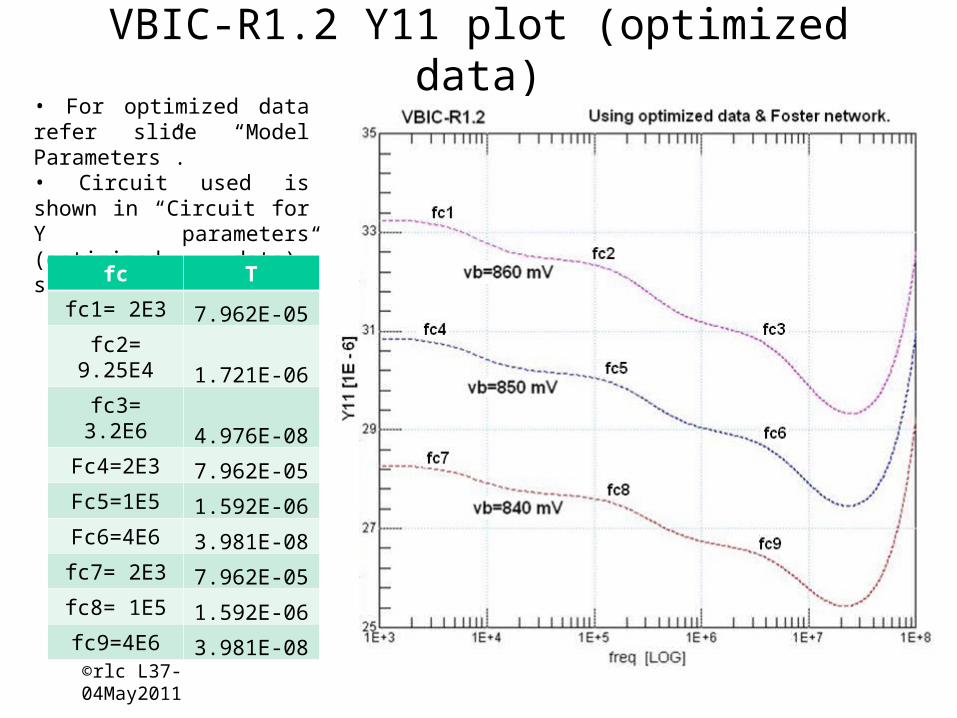
VBIC-R1.2 Y11 plot (optimized data)• For optimized data refer slide “Model Parameters”. • Circuit used is shown in “Circuit for Y parameters (optimized data)” slide.
fc Τ
fc1= 2E3 7.962E-05fc2=
9.25E4 1.721E-06fc3= 3.2E6 4.976E-08
Fc4=2E3 7.962E-05Fc5=1E5 1.592E-06Fc6=4E6 3.981E-08fc7= 2E3 7.962E-05fc8= 1E5 1.592E-06fc9=4E6 3.981E-08©rlc L37-04May2011

Spreadsheet for Calculating the Rth and Cth• Calculations mentioned in the previous slides have
been implemented in an Excel spreadsheet.• The Cauer to Foster network transformation is done.
• The spreadsheet takes the dimensions of different layers of the devices and gives corresponding Cauer and Foster network values. This enables the calculation of time constants which can be converted into a single pole. The characteristic times for the Foster network appear on a impulse response plot.
©rlc L37-04May2011
Fig. 7. Electrical equivalent Cauer network of the HBT Fig. 8. Electrical equivalent Foster network of the HBT

©rlc L37-04May2011
Effect of Rth on current feedback op-amp settling time
-
+
vIN = 1 V P-P, = 200 -sec
500
500
vOUT
100
max,IN
OUTmax,OUT
Av
tvvOffset

©rlc L37-04May2011
y = 0.0055e-0.1416x
Offset = 0.16%Tau = 7.1 u-sec
y = 0.0039e-0.0749x
Offset = .39%Tau = 13.4 u-sec
0.01%
0.10%
1.00%
0 5 10 15 20 25 30Time after switching (u-sec)
Th
erm
al
sw
itc
hin
g o
ffs
et
as
%
of
Vp
Current Feedback Op Amp Data (LMH6704) Switching Offset
3.3/t4.13/t e%16.0e%39.0model cfoa
3.34.13/%39.07.7/%55.0
%16.0Tau

©rlc L37-04May2011
LMH6550 impulse thermal characteristics
• LeCroy sampling oscilloscope (1M input mode)
• Maximum averaging (10000)• Input nominally +/- 1V with 50 micro-
sec period and 50% duty cycle.• Fractional Gain Error = FGE
1
vv
)t(v)t(v
FGE
max,IN
max,OUT
IN
OUT

©rlc L37-04May2011
vIN Rising Response
y = 0.0362e-111568x
R2 = 0.9707,Tau = 9 micro-sec
0.0
0.2
0.4
0.6
0.8
1.0
1.2
0.0E+00 5.0E-06 1.0E-05 1.5E-05 2.0E-05
0.10%
1.00%
10.00%
vOUT
vIN
FGE
©rlc L37-04May2011
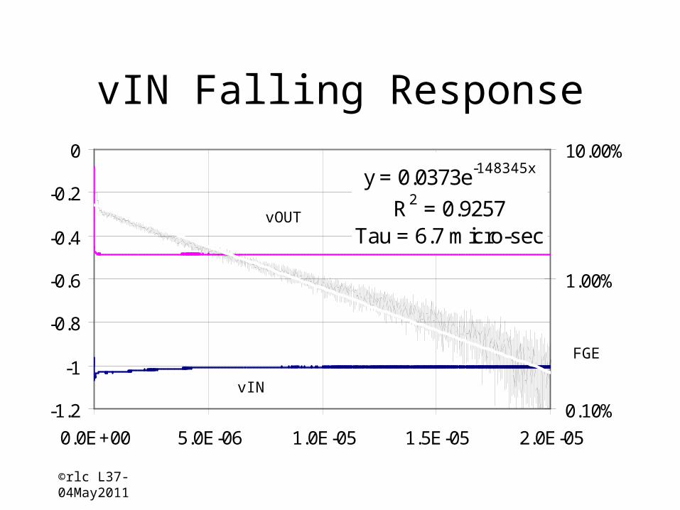
y = 0.0373e-148345x
R2 = 0.9257Tau = 6.7 micro-sec
-1.2
-1
-0.8
-0.6
-0.4
-0.2
0
0.0E+00 5.0E-06 1.0E-05 1.5E-05 2.0E-05
0.10%
1.00%
10.00%
vIN Falling Response
vOUT
vIN
FGE

Current Feedback Op-Amp (CFOA) with Simple Current Mirror (CM) Bias
STICK1
VEE
VEE
VCC
VCC
Q1 Q2
Q3 Q4(stk2-pnp-cm)
Q11 Q12
Q9 Q10 Q17
Q18
Q14
Q13
Q15
Q16
VOZ
VN
STICK2 STICK3 STICK4 STICK5 STICK6
VEE
VCC
Q6
Q5
Q7(stk3-npn-bf)
Q8(stk3-pnp-bf)
VP
RF
200 μA
+1 V
-1 V
sup
©rlc L37-04May2011

Large-signal Output Voltage Transient Analysis for CFOA with
Simple CM Biasing
0 5 10 15 20 25 30 35 40 45-978
-976
-974
-972
-970
-968
Time (s)
Vo
ltag
e (
mV
)
0 5 10 15 20 25 30 35 40 45
1020
1022
1024
1026
1028
Time (s)
Vo
ltag
e (
mV
)
High-to-Low area x1
High-to-Low area x8
Low-to-High area x1
Low-to-High area x8
TT=-5311 V
TT=5313 V
TT=789 V
TT=-789 V
©rlc L37-04May2011

Hypothesis: The Thermal Tail is a Linear Superposition of the Contribution from each
Individual Circuit Stick• The contribution of individual transistor to the total thermal
tail.
• Used six stick classifications according to transistor type and functionality.
i.e. Q10stk3-pnp-bf and Q11stk4-npn-cm
• Enabled the self-heating effect in the stick of interest and disabled the self-heating effect of the remaining transistors.
• Simulated the contribution of each individual stick.
• The total thermal tail simulated is essentially the sum of the individual thermal tail contributions of each circuit stick.
©rlc L37-04May2011

The Hypothesis Supported Area x1 Area x8
Thermal Tail (uV/V) High-to-Low Low-to-High High-to-Low Low-to-High
stk2-npn-bf (Q5) -822 842 -124 128
stk2-pnp-bf (Q6) -727 712 -101 98
stk2-npn-cm (Q2) -89 91 -11 12
stk2-pnp-cm (Q4) -91 89 -10 9
stk3-npn-bf (Q7) -877 850 -111 106
stk3-pnp-bf (Q8) -783 808 -111 115
stk4-npn-cm (Q12) -1213 1217 -172 173
stk4-pnp-cm (Q10) -1075 1073 -159 158
stk5-npn-bf(Q13) 13 -13 2 -2
stk5-pnp-bf(Q14) -4 4 -1 1
stk5-npn-cm(Q18) 16 -15 2 -2
stk5-pnp-cm(Q17) -5 2 0 0
stk6-npn-bf(Q15) 0 1 0 0
stk6-pnp-bf(Q16) -1 0 0 0
added total -5658 5661 -796 796
simulated total -5311 5313 -789 789©rlc L37-04May2011

©rlc L37-04May2011
References• Fujiang Lin, et al, “Extraction Of VBIC Model for SiGe HBTs
Made Easy by Going Through Gummel-Poon Model”, from http://eesof.tm.agilent.com/pdf/VBIC_Model_Extraction.pdf
• http://www.fht-esslingen.de/institute/iafgp/neu/VBIC/• Avanti Star-spice User Manual, 04, 2001. • Affirma Spectre Circuit Simulator Device Model Equations• Zweidinger, D.T.; Fox, R.M., et al, “Equivalent circuit
modeling of static substrate thermal coupling using VCVS representation”, Solid-State Circuits, IEEE Journal of , Volume: 2 Issue: 9 , Sept. 2002, Page(s): 1198 -1206

Thermal Analogy References
[1] I.Z. Mitrovic , O. Buiu, S. Hall, D.M. Bagnall and P. Ashburn “Review of SiGe HBTs on SOI”, Solid State Electronics, Sept. 2005, Vol. 49, pp. 1556-1567.
[2] Masana, F. N., “A New Approach to the Dynamic Thermal Modeling of Semiconductor Packages”, Microelectron. Reliab., 41, 2001, pp. 901–912.
[3] Richard C. Joy and E. S. Schlig, “Thermal Properties of Very Fast Transistors”, IEEE Trans. ED, ED-1 7. No. 8, August 1970, pp. 586-599.
[4] Kevin Bastin, “Analysis and Modeling of self heating in SiGe HBTs” , Aug. 2009, Masters Thesis, UTA.
[5] Rinaldi, N., “On the Modeling of the Transient Thermal Behavior of Semiconductor Devices”, IEEE Trans-ED, Volume: 48 , Issue: 12 , Dec. 2001; Pages:2796 – 2802.
©rlc L37-04May2011

Simulation … References
• [1] E. Castro, S. Coco, A. Laudani, L. LO Nigro and G. Pollicino, “A New Tool For Bipolar Transistor Characterization Based on HICUM”, Communications to SIMAI Congress, ISSN 1827-9015, Vol. 2, 2007.
• [2] K. Bastin, “Analysis And Modeling of Self Heating in Silicon Germanium Heterojunction Bipolar Transistors”, Thesis report, The University of Texas at Arlington, August 2009.
©rlc L37-04May2011

AICR Team at University of Texas Arlington - Electrical
EngineeringCurrent
• Ronald L. Carter, Professor
• W. Alan Davis, Associate Professor
• Howard T. Russell, Senior Lecturer
• Ardasheir Rahman1
• Xuesong Xie3
• Arun Thomas-Karingada2
• Sharath Patil2
• Valay Shah2
Earlier Contributors• Kevin Bastin, MS• Abhijit Chaugule, MS• Daewoo Kim, PhD• Anurag Lakhlani, MS• Zheng Li, PhD• Kamal Sinha, PhD
1PhD Student2MS Student3Post-doctoral Associate
©rlc L37-04May2011

©rlc L37-04May2011
References
• CARM = Circuit Analysis Reference Manual, MicroSim Corporation, Irvine, CA, 1995.
• M&A = Semiconductor Device Modeling with SPICE, 2nd ed., by Paolo Antognetti and Giuseppe Massobrio, McGraw-Hill, New York, 1993.
• **M&K = Device Electronics for Integrated Circuits, 2nd ed., by Richard S. Muller and Theodore I. Kamins, John Wiley and Sons, New York, 1986.
• *Semiconductor Physics and Devices, by Donald A. Neamen, Irwin, Chicago, 1997