EE 5340 Semiconductor Device Theory Lecture 6 - Fall 2010 Professor Ronald L. Carter [email protected] .
38
EE 5340 Semiconductor Device Theory Lecture 6 - Fall 2010 Professor Ronald L. Carter [email protected] http://www.uta.edu/ronc
-
Upload
shon-mills -
Category
Documents
-
view
253 -
download
2
Transcript of EE 5340 Semiconductor Device Theory Lecture 6 - Fall 2010 Professor Ronald L. Carter [email protected] .
EE 5340Semiconductor Device TheoryLecture 6 - Fall 2010
Professor Ronald L. [email protected]
http://www.uta.edu/ronc

L06 10Sep10
Second Assignment
• Please print and bring to class a signed copy of the document appearing at
http://www.uta.edu/ee/COE%20Ethics%20Statement%20Fall%2007.pdf
2
L06 10Sep10 3
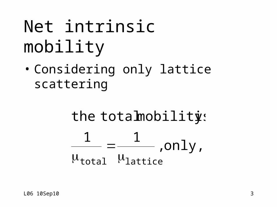
Net intrinsicmobility• Considering only lattice scattering
only, , 11
is mobility total the
latticetotal
L06 10Sep10 4
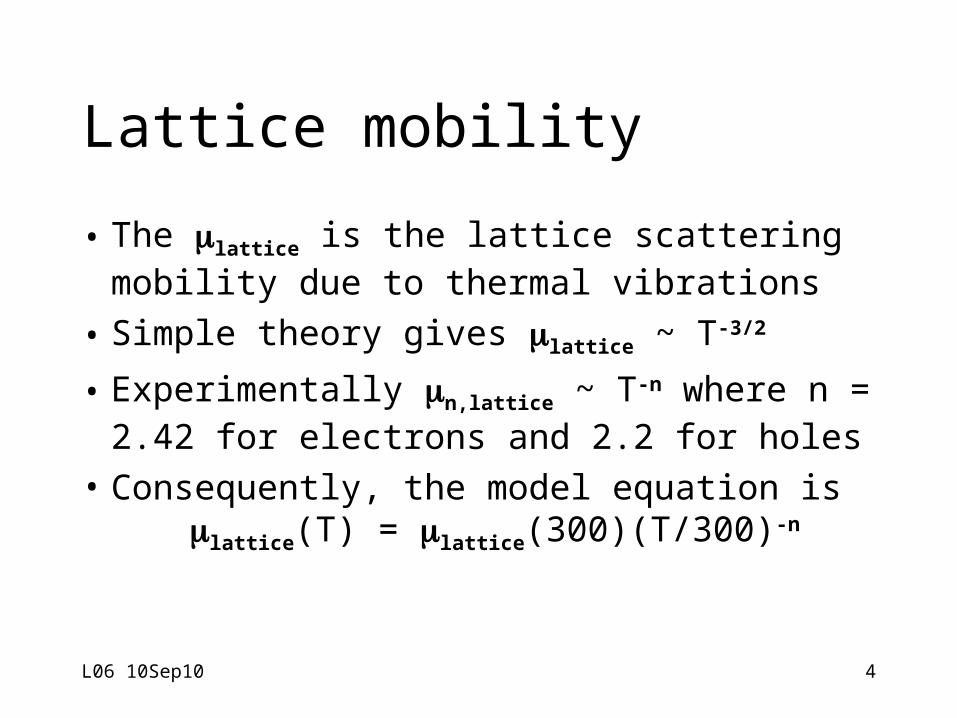
Lattice mobility
• The lattice is the lattice scattering mobility due to thermal vibrations
• Simple theory gives lattice ~ T-3/2
• Experimentally n,lattice ~ T-n where n = 2.42 for electrons and 2.2 for holes
• Consequently, the model equation is lattice(T) = lattice(300)(T/300)-n
L06 10Sep10 5
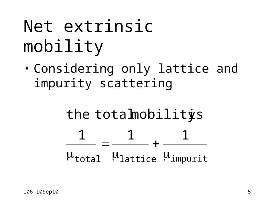
Net extrinsicmobility• Considering only lattice and
impurity scattering
impuritylatticetotal
111
is mobility total the
L06 10Sep10 6
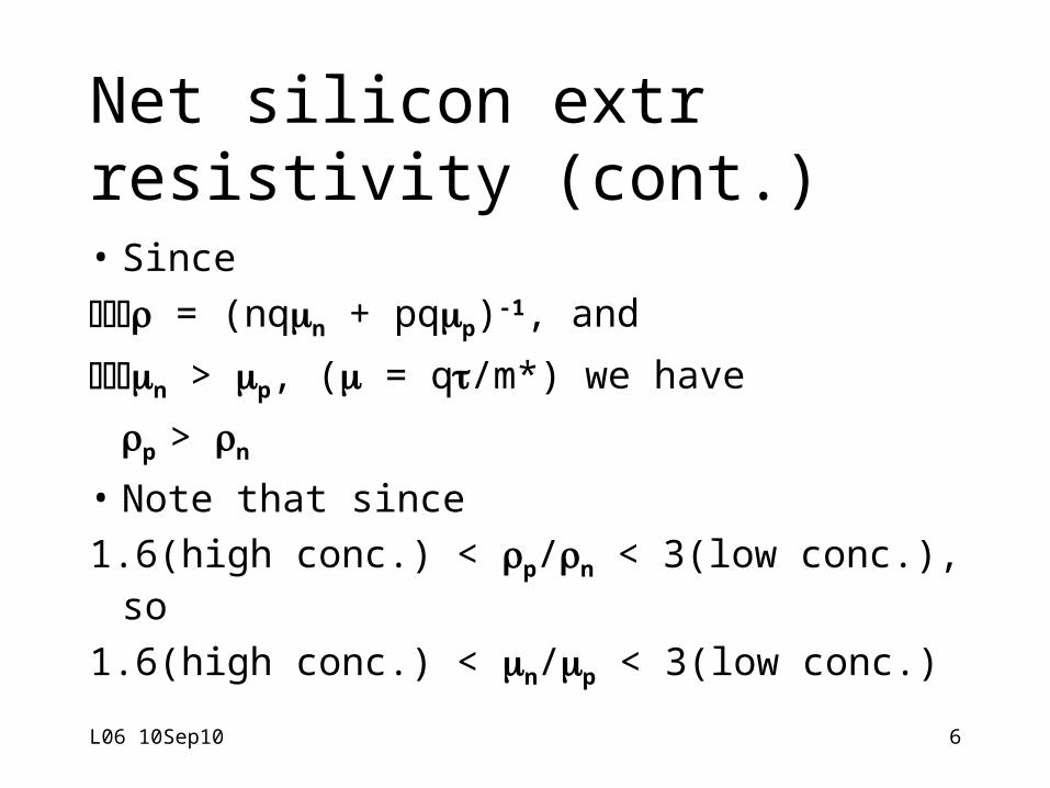
Net silicon extrresistivity (cont.)• Since = (nqn + pqp)-1, and
n > p, ( = q/m*) we have
p > n
• Note that since1.6(high conc.) < p/n < 3(low conc.), so
1.6(high conc.) < n/p < 3(low conc.)
L06 10Sep10 7
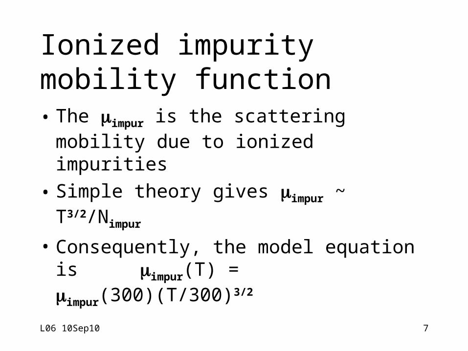
Ionized impuritymobility function• The impur is the scattering mobility
due to ionized impurities
• Simple theory gives impur ~ T3/2/Nimpur
• Consequently, the model equation is impur(T) = impur(300)
(T/300)3/2
L06 10Sep10 8
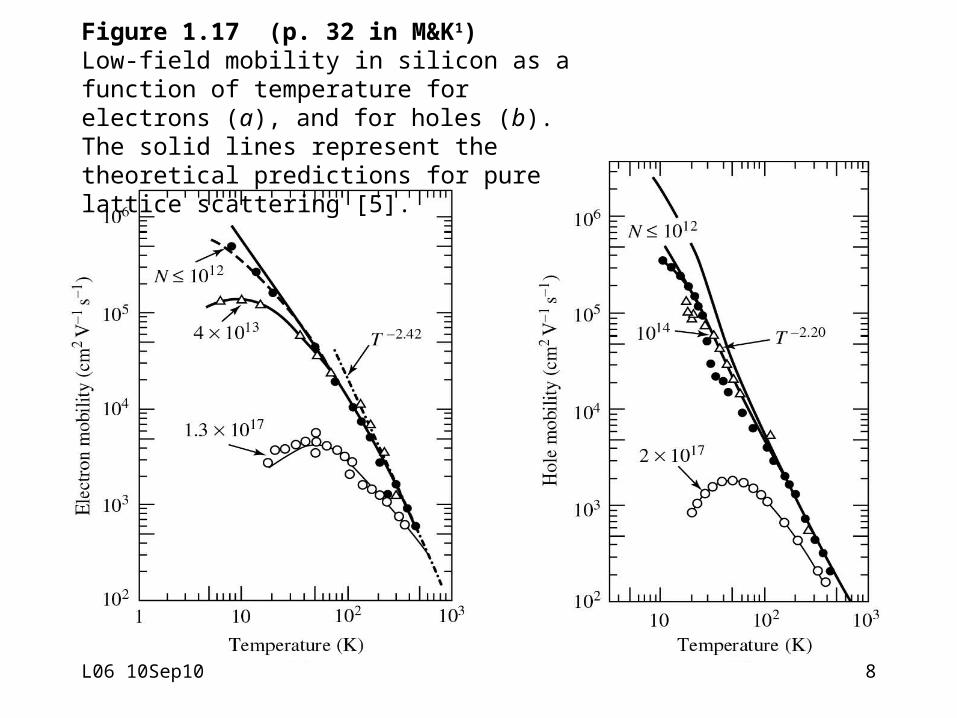
Figure 1.17 (p. 32 in M&K1) Low-field mobility in silicon as a function of temperature for electrons (a), and for holes (b). The solid lines represent the theoretical predictions for pure lattice scattering [5].
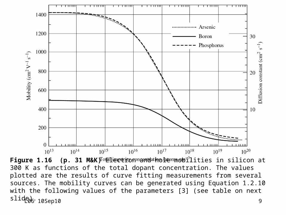
Figure 1.16 (p. 31 M&K) Electron and hole mobilities in silicon at 300 K as functions of the total dopant concentration. The values plotted are the results of curve fitting measurements from several sources. The mobility curves can be generated using Equation 1.2.10 with the following values of the parameters [3] (see table on next slide).
L06 10Sep10 9
L06 10Sep10 10
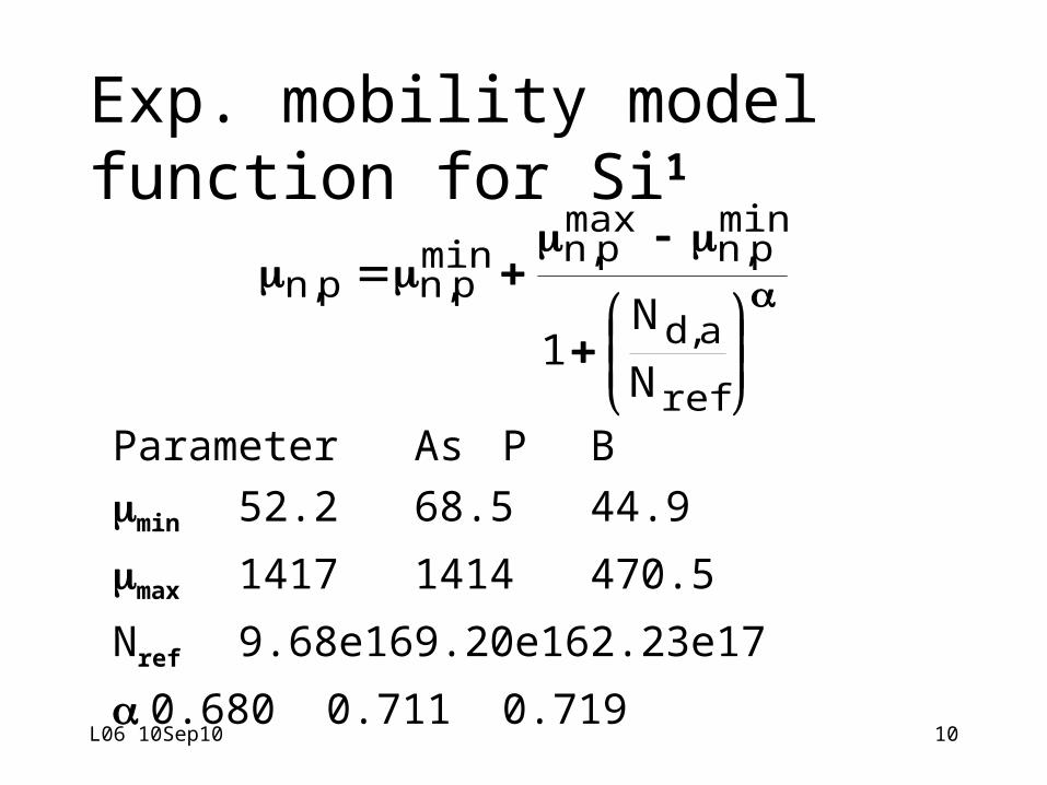
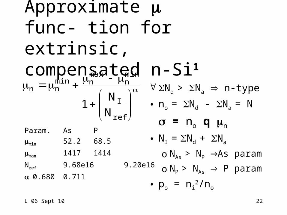
Exp. mobility modelfunction for Si1
Parameter As P Bmin 52.2 68.5 44.9
max 1417 1414 470.5
Nref 9.68e169.20e162.23e17
0.680 0.711 0.719
ref
a,d
minpn,
maxpn,min
pn,pn,
N
N1
L06 10Sep10 11
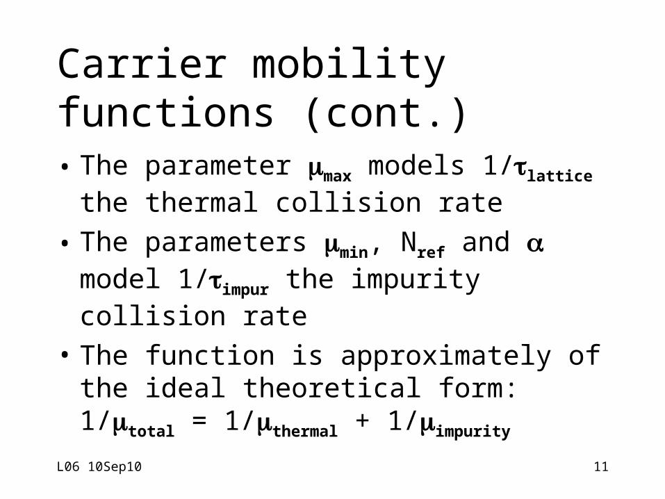
Carrier mobilityfunctions (cont.)• The parameter max models 1/lattice
the thermal collision rate
• The parameters min, Nref and model 1/impur the impurity collision rate
• The function is approximately of the ideal theoretical form:
1/total = 1/thermal + 1/impurity
L06 10Sep10 12
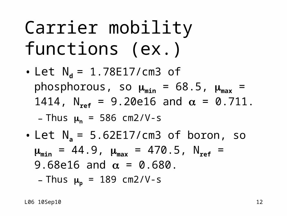
Carrier mobilityfunctions (ex.)• Let Nd
= 1.78E17/cm3 of phosphorous, so min = 68.5, max = 1414, Nref = 9.20e16 and = 0.711. – Thus n = 586 cm2/V-s
• Let Na = 5.62E17/cm3 of boron, so min
= 44.9, max = 470.5, Nref = 9.68e16 and = 0.680. – Thus p = 189 cm2/V-s
L06 10Sep10 13
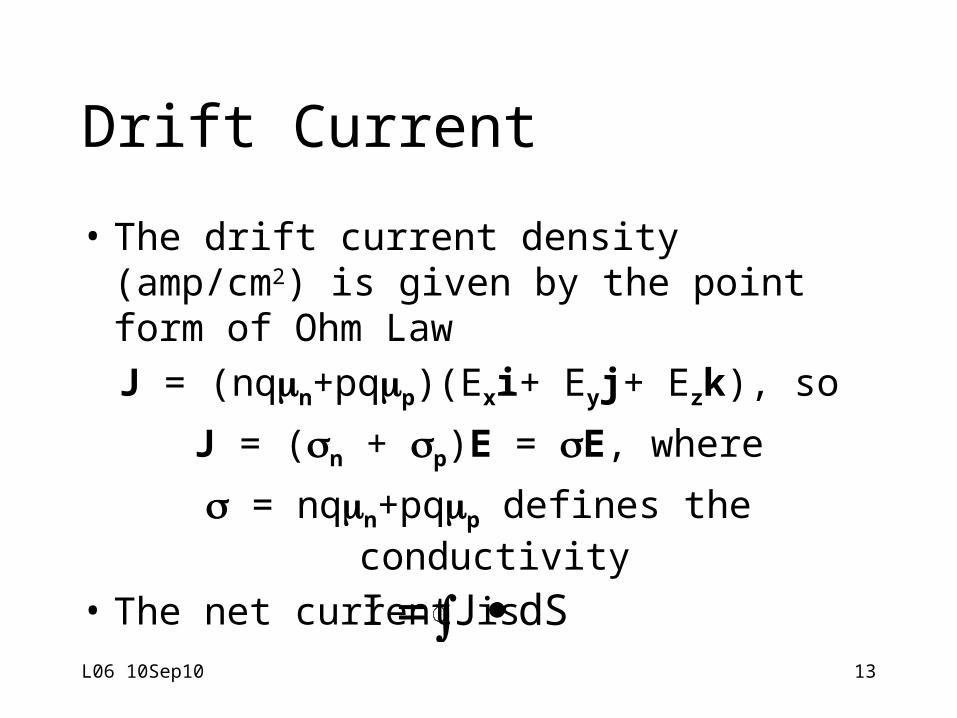
Drift Current
• The drift current density (amp/cm2) is given by the point form of Ohm LawJ = (nqn+pqp)(Exi+ Eyj+ Ezk), so
J = (n + p)E = E, where
= nqn+pqp defines the conductivity
• The net current is SdJI
L06 10Sep10 14
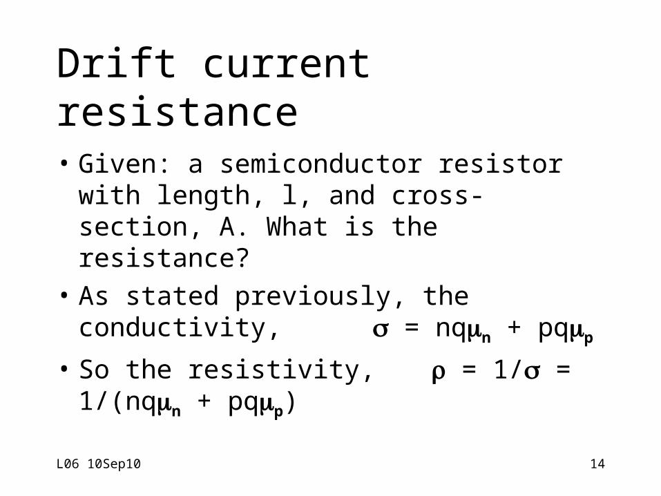
Drift currentresistance• Given: a semiconductor resistor with
length, l, and cross-section, A. What is the resistance?
• As stated previously, the conductivity,
= nqn + pqp
• So the resistivity, = 1/ = 1/(nqn + pqp)
L06 10Sep10 15
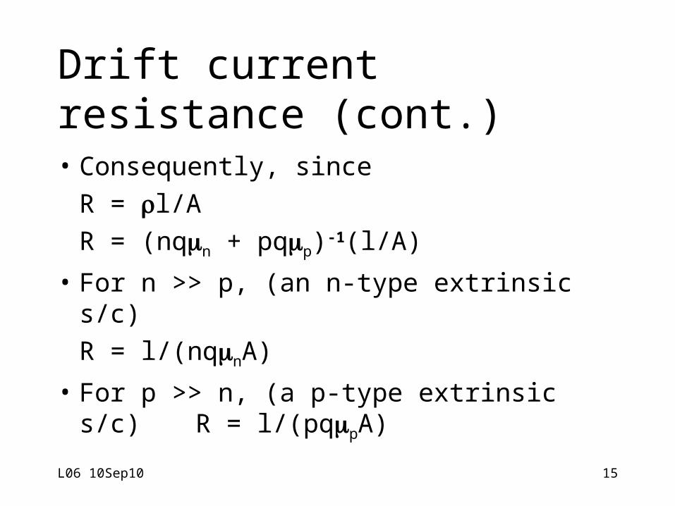
Drift currentresistance (cont.)• Consequently, since
R = l/AR = (nqn + pqp)-1(l/A)
• For n >> p, (an n-type extrinsic s/c)R = l/(nqnA)
• For p >> n, (a p-type extrinsic s/c) R = l/(pqpA)
L06 10Sep10 16
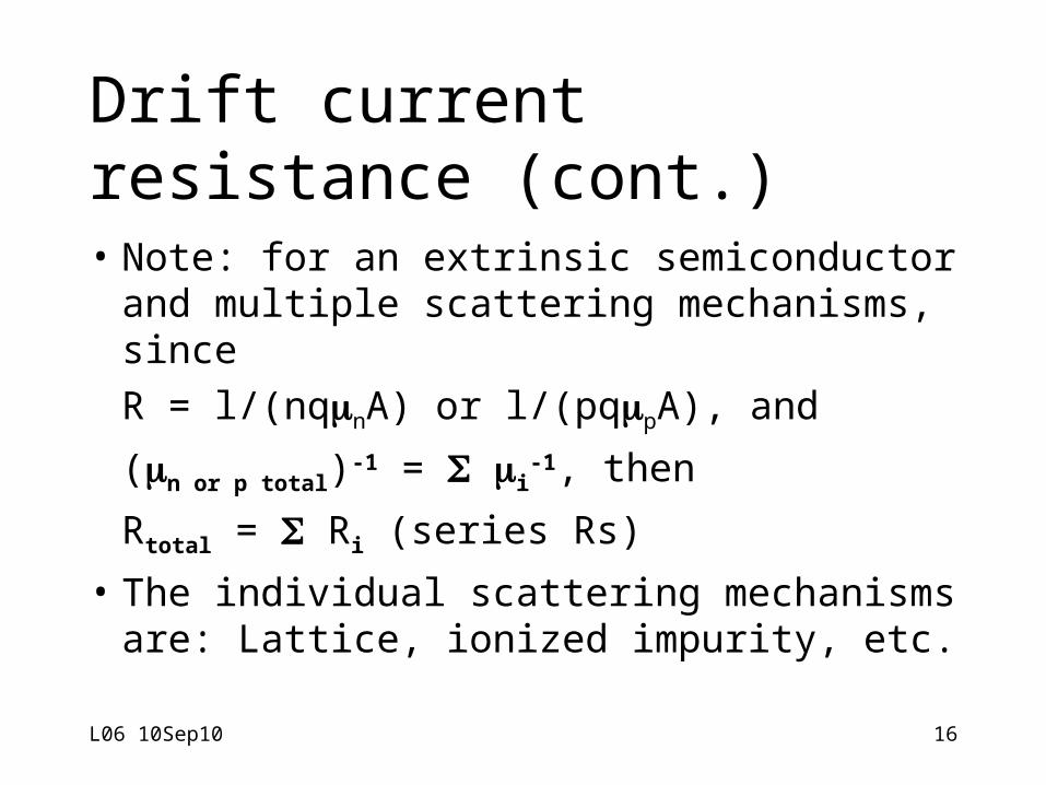
Drift currentresistance (cont.)• Note: for an extrinsic semiconductor
and multiple scattering mechanisms, since
R = l/(nqnA) or l/(pqpA), and
(n or p total)-1 = i-1, then
Rtotal = Ri (series Rs)
• The individual scattering mechanisms are: Lattice, ionized impurity, etc.
L06 10Sep10 17
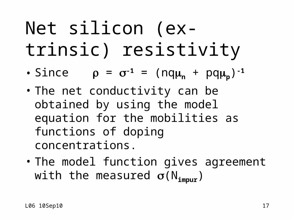
Net silicon (ex-trinsic) resistivity• Since = -1 = (nqn + pqp)-1
• The net conductivity can be obtained by using the model equation for the mobilities as functions of doping concentrations.
• The model function gives agreement with the measured (Nimpur)
L06 10Sep10 18
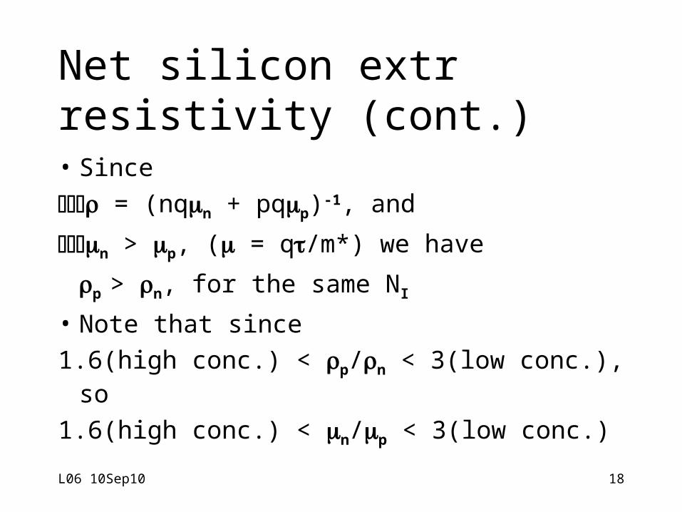
Net silicon extrresistivity (cont.)• Since = (nqn + pqp)-1, and
n > p, ( = q/m*) we have
p > n, for the same NI
• Note that since1.6(high conc.) < p/n < 3(low conc.), so
1.6(high conc.) < n/p < 3(low conc.)
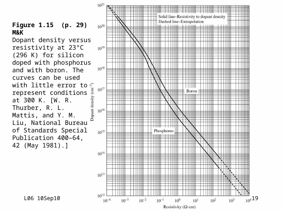
Figure 1.15 (p. 29) M&K Dopant density versus resistivity at 23°C (296 K) for silicon doped with phosphorus and with boron. The curves can be used with little error to represent conditions at 300 K. [W. R. Thurber, R. L. Mattis, and Y. M. Liu, National Bureau of Standards Special Publication 400–64, 42 (May 1981).]
L06 10Sep10 19
L 06 Sept 10 20
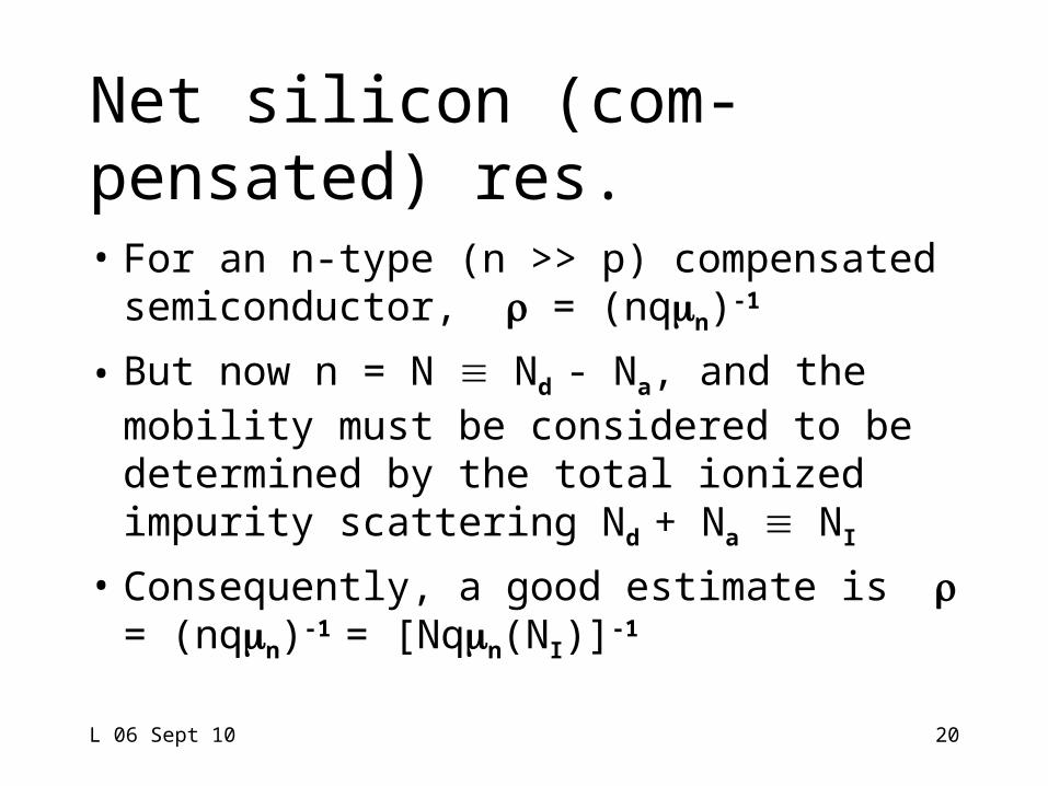
Net silicon (com-pensated) res.• For an n-type (n >> p) compensated
semiconductor, = (nqn)-1
• But now n = N Nd - Na, and the mobility must be considered to be determined by the total ionized impurity scattering Nd + Na NI
• Consequently, a good estimate is = (nqn)-1 = [Nqn(NI)]-1
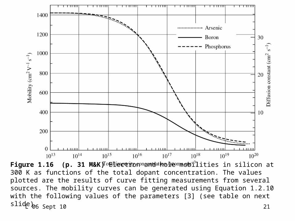
Figure 1.16 (p. 31 M&K) Electron and hole mobilities in silicon at 300 K as functions of the total dopant concentration. The values plotted are the results of curve fitting measurements from several sources. The mobility curves can be generated using Equation 1.2.10 with the following values of the parameters [3] (see table on next slide).
L 06 Sept 10 21
L 06 Sept 10 22
Approximate func- tion for extrinsic, compensated n-Si1
Param. As Pmin 52.2 68.5
max 1417 1414
Nref 9.68e169.20e16
0.680 0.711
ref
I
minn
maxnmin
nn
NN
1
Nd > Na n-type
• no = Nd - Na = N
= no q n
• NI = Nd + Na
o NAs > NP As param
o NP > NAs P param
• po = ni2/no
L 06 Sept 10 23
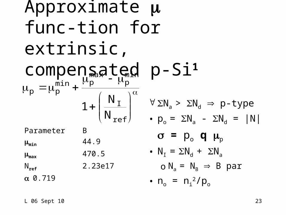
Approximate func-tion for extrinsic, compensated p-Si1
Parameter Bmin 44.9
max 470.5
Nref 2.23e17
0.719
ref
I
minp
maxpmin
pp
NN
1 Na > Nd p-type
• po = Na - Nd = |N|
= po q p
• NI = Nd + Na
o Na = NB B par
• no = ni2/po
L 06 Sept 10 24
Summary
• The concept of mobility introduced as a response function to the electric field in establishing a drift current
• Resistivity and conductivity defined
• (Nd,Na,T) model equation developed
• Resistivity models developed for extrinsic and compensated materials
L06 10Sep10 25
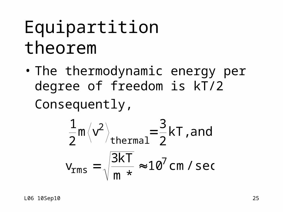
Equipartitiontheorem• The thermodynamic energy per
degree of freedom is kT/2Consequently,
sec/cm10*m
kT3v
and ,kT23
vm21
7rms
thermal2
L06 10Sep10 26
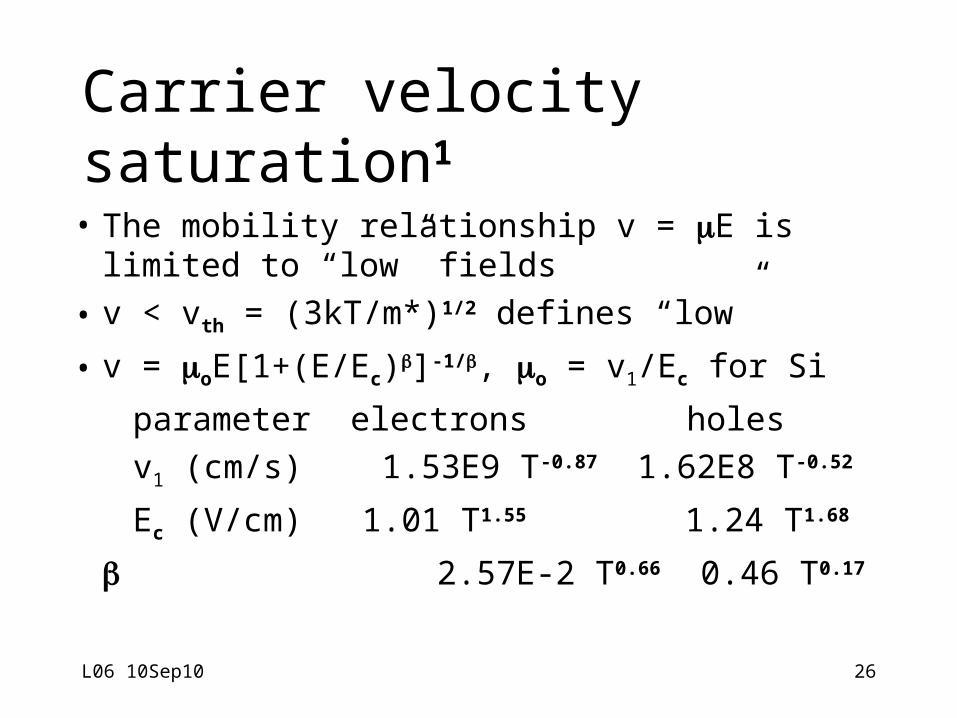
Carrier velocitysaturation1
• The mobility relationship v = E is limited to “low” fields
• v < vth = (3kT/m*)1/2 defines “low”
• v = oE[1+(E/Ec)]-1/, o = v1/Ec for Si
parameter electrons holes v1 (cm/s) 1.53E9 T-0.87 1.62E8 T-0.52
Ec (V/cm) 1.01 T1.55 1.24 T1.68
2.57E-2 T0.66 0.46 T0.17
L06 10Sep10 27
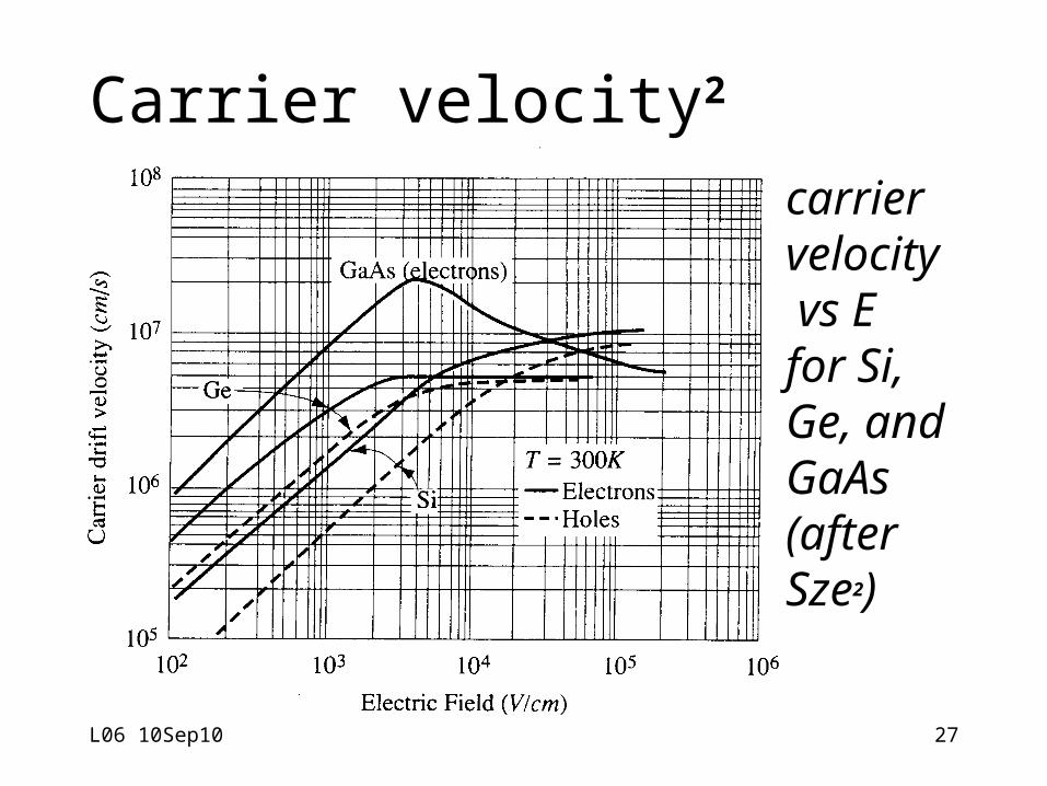
Carrier velocity2
carriervelocity vs Efor Si,Ge, andGaAs(afterSze2)
L06 10Sep10 28
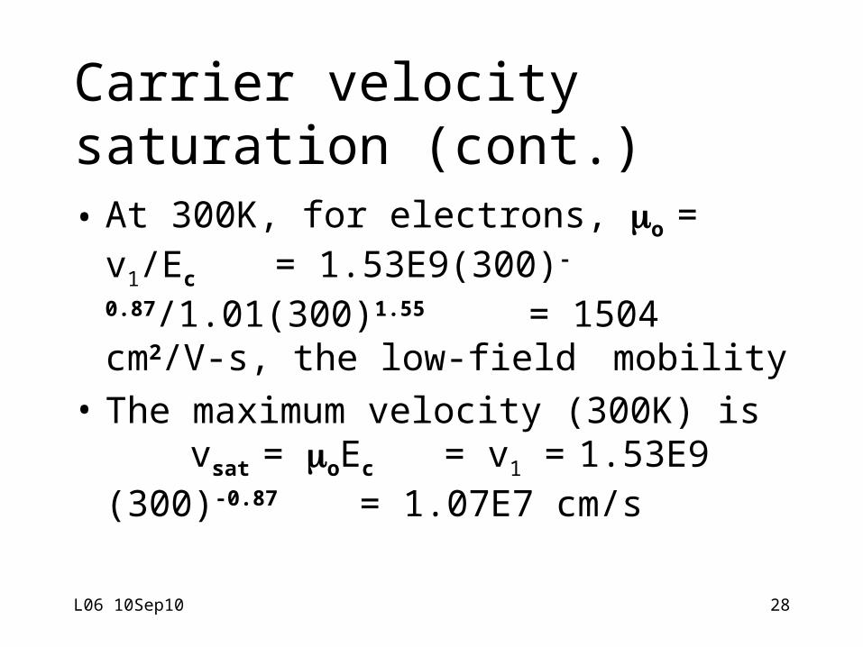
Carrier velocitysaturation (cont.)• At 300K, for electrons, o = v1/Ec
= 1.53E9(300)-0.87/1.01(300)1.55 = 1504 cm2/V-s, the low-field
mobility• The maximum velocity (300K) is
vsat = oEc = v1 = 1.53E9 (300)-
0.87 = 1.07E7 cm/s
L06 10Sep10 29
Diffusion ofCarriers (cont.)
L06 10Sep10 30
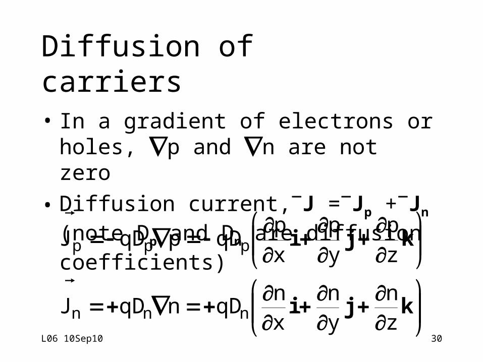
Diffusion ofcarriers• In a gradient of electrons or holes,
p and n are not zero
• Diffusion current,J =Jp +Jn (note Dp and Dn are diffusion coefficients)
kji
kji
zn
yn
xn
qDnqDJ
zp
yp
xp
qDpqDJ
nnn
ppp
L06 10Sep10 31
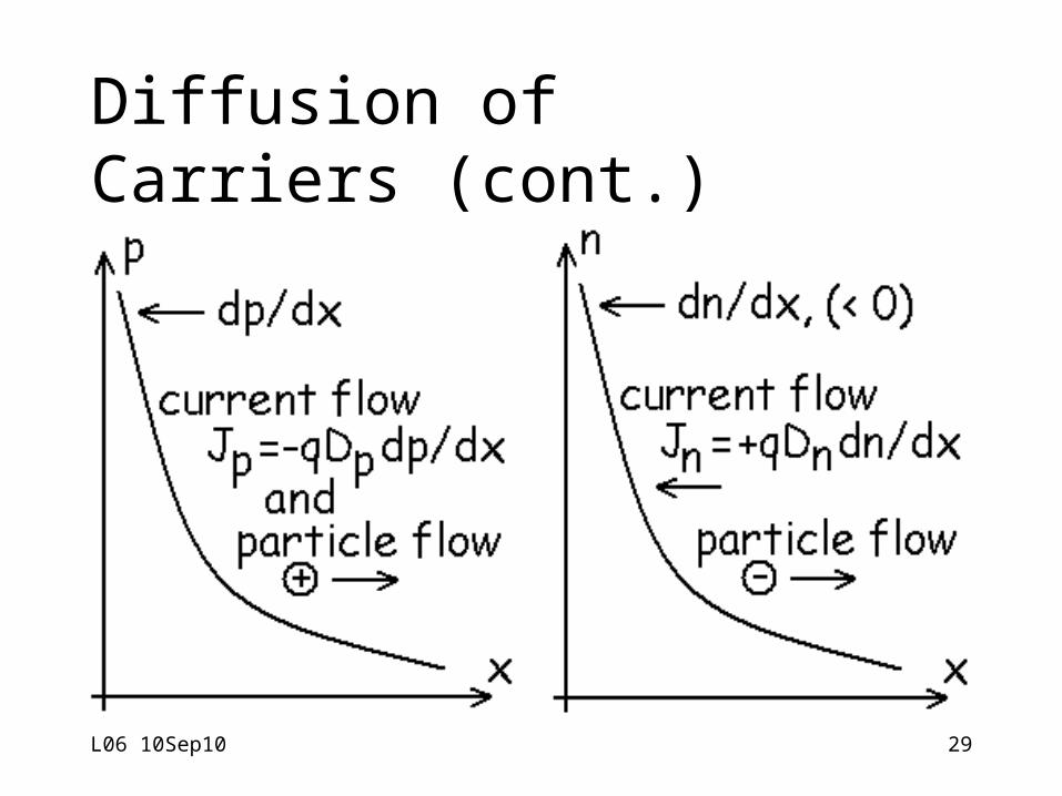
Diffusion ofcarriers (cont.)• Note (p)x has the magnitude of
dp/dx and points in the direction of increasing p (uphill)
• The diffusion current points in the direction of decreasing p or n (downhill) and hence the - sign in the definition ofJp and the + sign in the definition ofJn
L06 10Sep10 32
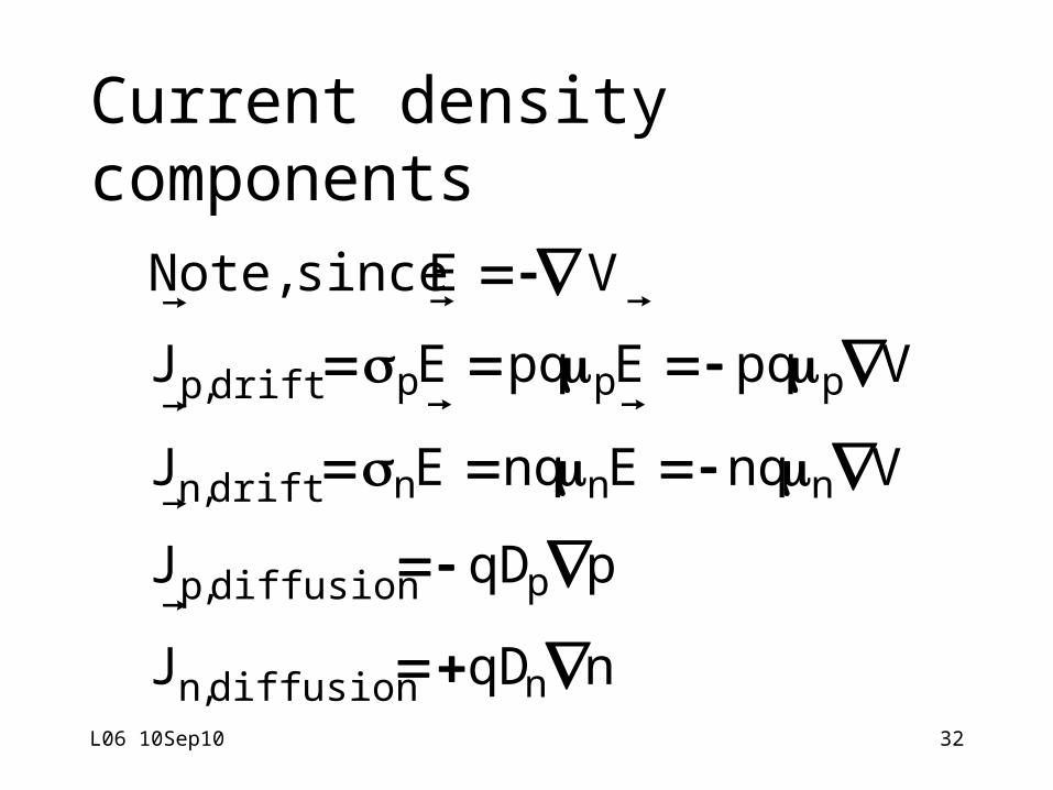
Current densitycomponents
nqDJ
pqDJ
VnqEnqEJ
VpqEpqEJ
VE since Note,
ndiffusion,n
pdiffusion,p
nnndrift,n
pppdrift,p
L06 10Sep10 33
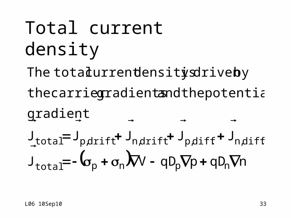
Total currentdensity
nqDpqDVJ
JJJJJ
gradient
potential the and gradients carrier the
by driven is density current total The
npnptotal
.diff,n.diff,pdrift,ndrift,ptotal
L06 10Sep10 34
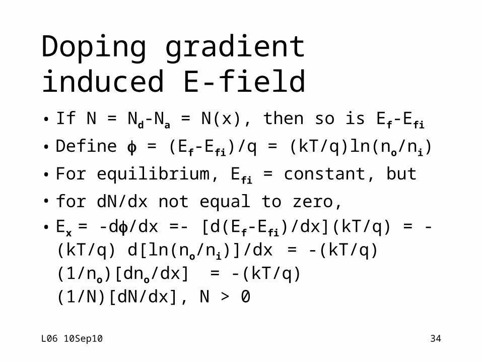
Doping gradient induced E-field• If N = Nd-Na = N(x), then so is Ef-Efi
• Define = (Ef-Efi)/q = (kT/q)ln(no/ni)
• For equilibrium, Efi = constant, but
• for dN/dx not equal to zero,
• Ex = -d/dx =- [d(Ef-Efi)/dx](kT/q)= -(kT/q) d[ln(no/ni)]/dx = -(kT/q) (1/no)[dno/dx] = -(kT/q) (1/N)[dN/dx], N > 0
L06 10Sep10 35
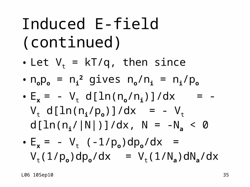
Induced E-field(continued)• Let Vt = kT/q, then since
• nopo = ni2 gives no/ni = ni/po
• Ex = - Vt d[ln(no/ni)]/dx = - Vt d[ln(ni/po)]/dx = - Vt d[ln(ni/|N|)]/dx, N = -Na < 0
• Ex = - Vt (-1/po)dpo/dx = Vt(1/po)dpo/dx = Vt(1/Na)dNa/dx
L06 10Sep10 36
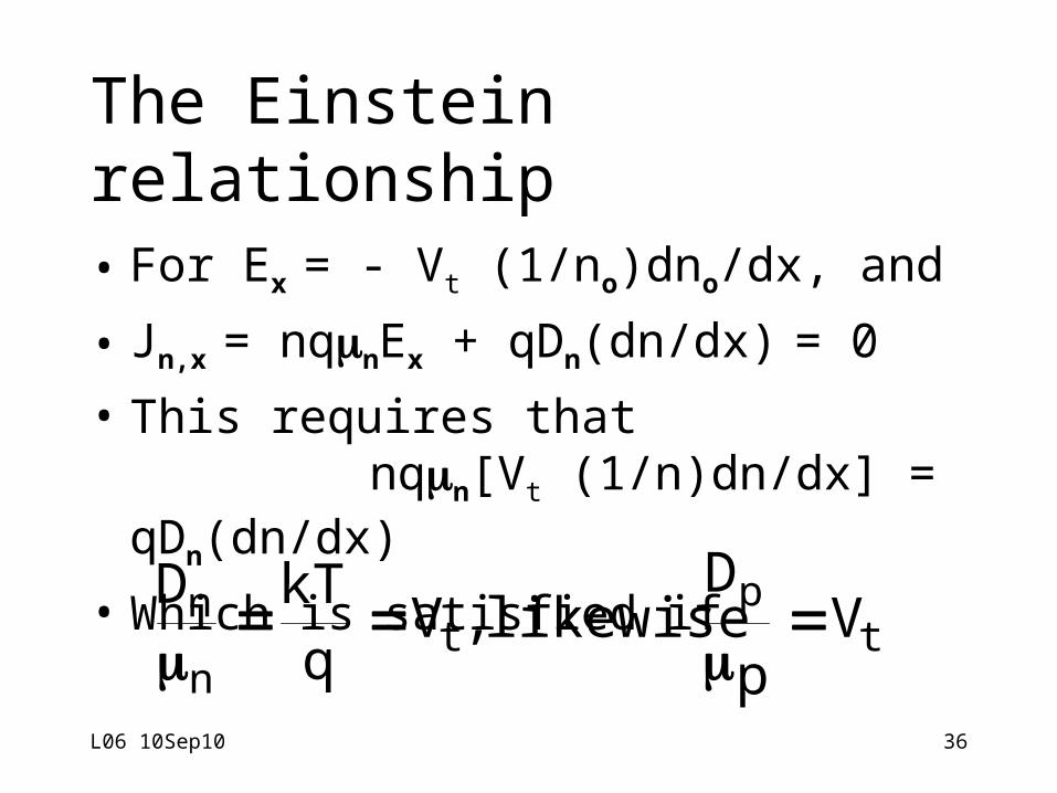
The Einsteinrelationship• For Ex = - Vt (1/no)dno/dx, and
• Jn,x = nqnEx + qDn(dn/dx) = 0
• This requires that nqn[Vt (1/n)dn/dx] =
qDn(dn/dx)
• Which is satisfied if tp
tn
n Vp
D likewise ,V
qkTD
L06 10Sep10
References
*Fundamentals of Semiconductor Theory and Device Physics, by Shyh Wang, Prentice Hall, 1989.
** and 3Semiconductor Physics & Devices, by Donald A. Neamen, 2nd ed., Irwin, Chicago.
M&K = Device Electronics for Integrated Circuits, 3rd ed., by Richard S. Muller, Theodore I. Kamins, and Mansun Chan, John Wiley and Sons, New York, 2003.
37
L06 10Sep10 38
References
M&K and 1Device Electronics for Integrated Circuits, 2 ed., by Muller and Kamins, Wiley, New York, 1986.– See Semiconductor Device Fundamen-
tals, by Pierret, Addison-Wesley, 1996, for another treatment of the model.
2Physics of Semiconductor Devices, by S. M. Sze, Wiley, New York, 1981.