Document Number: MW7IC2020N Technical Data RF LDMOS Wideband Integrated Power...
17
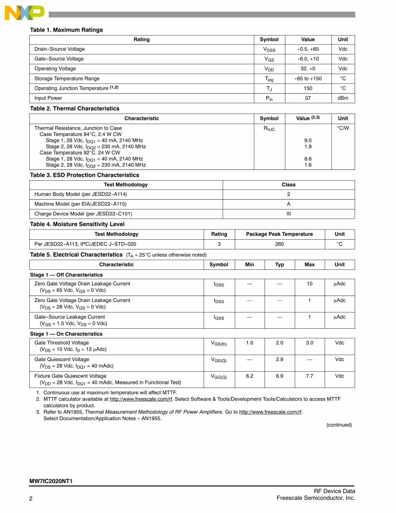
RF LDMOS Wideband Integrated Power Amplifier The MW7IC2020N wideband integrated circuit is designed with on--chip matching that makes it usable from 1805 to 2170 MHz. This multi--stage structure is rated for 26 to 32 Volt operation and covers all typical cellular base station modulation formats. Driver Application — 2100 MHz Typical Single--Carrier W--CDMA Performance: V DD = 28 Volts, I DQ1 = 40 mA, I DQ2 = 230 mA, P out = 2.4 Watts Avg., IQ Magnitude Clipping, Channel Bandwidth = 3.84 MHz, Input Signal PAR = 7.5 dB @ 0.01% Probability on CCDF. Frequency G ps (dB) PAE (%) Output PAR (dB) ACPR (dBc) 2110 MHz 32.6 16.8 7.7 --51.3 2140 MHz 32.6 17.0 7.6 --51.4 2170 MHz 32.4 17.0 7.5 --51.6 Capable of Handling 10:1 VSWR, @ 32 Vdc, 2140 MHz, P out = 33 Watts CW (3 dB Input Overdrive from Rated P out ) Typical P out @ 1 dB Compression Point ≃ 20 Watts CW Driver Application — 1800 MHz Typical Single--Carrier W--CDMA Performance: V DD = 28 Volts, I DQ1 = 40 mA, I DQ2 = 230 mA, P out = 2.4 Watts Avg., IQ Magnitude Clipping, Channel Bandwidth = 3.84 MHz, Input Signal PAR = 7.5 dB @ 0.01% Probability on CCDF. Frequency G ps (dB) PAE (%) Output PAR (dB) ACPR (dBc) 1805 MHz 31.8 17.4 7.6 --51.2 1840 MHz 31.8 17.4 7.7 --50.2 1880 MHz 31.8 17.4 7.7 --51.0 Features Characterized with Series Equivalent Large--Signal Impedance Parameters and Common Source S--Parameters On--Chip Matching (50 Ohm Input, DC Blocked) Integrated Quiescent Current Temperature Compensation with Enable/Disable Function (1) Integrated ESD Protection In Tape and Reel. T1 Suffix = 1000 Units, 16 mm Tape Width, 13--inch Reel. Figure 1. Functional Block Diagram Figure 2. Pin Connections V GS2 V GS1 1 RF in Quiescent Current Temperature Compensation (1) RF in RF out /V DS2 V DS1 2 3 4 5 6 7 8 9 10 11 12 18 17 16 15 14 13 24 23 22 21 20 19 GND GND NC V DS1 V DS1 V GS1 V GS2 RF in NC NC NC NC NC NC NC RF out /V DS2 RF out /V DS2 NC NC NC NC NC NC 1. Refer to AN1977, Quiescent Current Thermal Tracking Circuit in the RF Integrated Circuit Family and to AN1987, Quiescent Current Control for the RF Integrated Circuit Device Family . Go to http://www.freescale.com/rf . Select Documentation/Application Notes -- AN1977 or AN1987. 1805--2170 MHz, 2.4 W AVG., 28 V SINGLE W--CDMA RF LDMOS WIDEBAND INTEGRATED POWER AMPLIFIER MW7IC2020NT1 PQFN 8 8 PLASTIC Document Number: MW7IC2020N Rev. 1, 12/2013 Freescale Semiconductor Technical Data Freescale Semiconductor, Inc., 2012--2013. All rights reserved.
Transcript of Document Number: MW7IC2020N Technical Data RF LDMOS Wideband Integrated Power...
MW7IC2020NT1
1RF Device DataFreescale Semiconductor, Inc.
RF LDMOS Wideband IntegratedPower AmplifierThe MW7IC2020N wideband integrated circuit is designed with on--chip
matching that makes it usable from 1805 to 2170 MHz. This multi--stagestructure is rated for 26 to 32 Volt operation and covers all typical cellular basestation modulation formats.
Driver Application — 2100 MHz Typical Single--Carrier W--CDMA Performance: VDD = 28 Volts, IDQ1 =
40 mA, IDQ2 = 230 mA, Pout = 2.4 Watts Avg., IQ Magnitude Clipping,Channel Bandwidth = 3.84 MHz, Input Signal PAR = 7.5 dB @ 0.01%Probability on CCDF.
FrequencyGps(dB)
PAE(%)
Output PAR(dB)
ACPR(dBc)
2110 MHz 32.6 16.8 7.7 --51.3
2140 MHz 32.6 17.0 7.6 --51.4
2170 MHz 32.4 17.0 7.5 --51.6
Capable of Handling 10:1 VSWR, @ 32 Vdc, 2140 MHz, Pout = 33 WattsCW (3 dB Input Overdrive from Rated Pout)
Typical Pout @ 1 dB Compression Point≃ 20 Watts CWDriver Application — 1800 MHz Typical Single--Carrier W--CDMA Performance: VDD = 28 Volts,
IDQ1 = 40 mA, IDQ2 = 230 mA, Pout = 2.4 Watts Avg., IQ MagnitudeClipping, Channel Bandwidth = 3.84 MHz, Input Signal PAR = 7.5 dB@ 0.01% Probability on CCDF.
FrequencyGps(dB)
PAE(%)
Output PAR(dB)
ACPR(dBc)
1805 MHz 31.8 17.4 7.6 --51.2
1840 MHz 31.8 17.4 7.7 --50.2
1880 MHz 31.8 17.4 7.7 --51.0
Features Characterized with Series Equivalent Large--Signal Impedance Parameters and Common Source S--Parameters On--Chip Matching (50 Ohm Input, DC Blocked) Integrated Quiescent Current Temperature Compensation with Enable/Disable Function (1)
Integrated ESD Protection In Tape and Reel. T1 Suffix = 1000 Units, 16 mm Tape Width, 13--inch Reel.
Figure 1. Functional Block Diagram Figure 2. Pin Connections
VGS2VGS1
1
RFin
Quiescent CurrentTemperature Compensation (1)
RFin RFout/VDS2
VDS1
23456 7 8 9 10 11 12
181716151413
24 23 22 21 20 19
GND
GND
NC
V DS1
V DS1
V GS1
V GS2
RFin
NC
NCNC
NC
NCNC
NC
RFout/VDS2RFout/VDS2
NC
NC
NC
NC
NCNC
1. Refer to AN1977,Quiescent Current Thermal Tracking Circuit in the RF Integrated Circuit Family and to AN1987,Quiescent Current Controlfor theRF IntegratedCircuit DeviceFamily.Go to http://www.freescale.com/rf. SelectDocumentation/ApplicationNotes -- AN1977orAN1987.
1805--2170 MHz, 2.4 W AVG., 28 VSINGLE W--CDMA
RF LDMOS WIDEBANDINTEGRATED POWER AMPLIFIER
MW7IC2020NT1
PQFN 8 8PLASTIC
Document Number: MW7IC2020NRev. 1, 12/2013
Freescale SemiconductorTechnical Data
Freescale Semiconductor, Inc., 2012--2013. All rights reserved.
2RF Device Data
Freescale Semiconductor, Inc.
MW7IC2020NT1
Table 1. Maximum Ratings
Rating Symbol Value Unit
Drain--Source Voltage VDSS --0.5, +65 Vdc
Gate--Source Voltage VGS --6.0, +10 Vdc
Operating Voltage VDD 32, +0 Vdc
Storage Temperature Range Tstg --65 to +150 C
Operating Junction Temperature (1,2) TJ 150 C
Input Power Pin 37 dBm
Table 2. Thermal Characteristics
Characteristic Symbol Value (2,3) Unit
Thermal Resistance, Junction to CaseCase Temperature 84C, 2.4 W CW
Stage 1, 28 Vdc, IDQ1 = 40 mA, 2140 MHzStage 2, 28 Vdc, IDQ2 = 230 mA, 2140 MHz
Case Temperature 92C, 24 W CWStage 1, 28 Vdc, IDQ1 = 40 mA, 2140 MHzStage 2, 28 Vdc, IDQ2 = 230 mA, 2140 MHz
RJC
9.01.9
8.61.6
C/W
Table 3. ESD Protection Characteristics
Test Methodology Class
Human Body Model (per JESD22--A114) 2
Machine Model (per EIA/JESD22--A115) A
Charge Device Model (per JESD22--C101) III
Table 4. Moisture Sensitivity Level
Test Methodology Rating Package Peak Temperature Unit
Per JESD22--A113, IPC/JEDEC J--STD--020 3 260 C
Table 5. Electrical Characteristics (TA = 25C unless otherwise noted)
Characteristic Symbol Min Typ Max Unit
Stage 1 — Off Characteristics
Zero Gate Voltage Drain Leakage Current(VDS = 65 Vdc, VGS = 0 Vdc)
IDSS — — 10 Adc
Zero Gate Voltage Drain Leakage Current(VDS = 28 Vdc, VGS = 0 Vdc)
IDSS — — 1 Adc
Gate--Source Leakage Current(VGS = 1.5 Vdc, VDS = 0 Vdc)
IGSS — — 1 Adc
Stage 1 — On Characteristics
Gate Threshold Voltage(VDS = 10 Vdc, ID = 12 Adc)
VGS(th) 1.0 2.0 3.0 Vdc
Gate Quiescent Voltage(VDS = 28 Vdc, IDQ1 = 40 mAdc)
VGS(Q) — 2.9 — Vdc
Fixture Gate Quiescent Voltage(VDD = 28 Vdc, IDQ1 = 40 mAdc, Measured in Functional Test)
VGG(Q) 6.2 6.9 7.7 Vdc
1. Continuous use at maximum temperature will affect MTTF.2. MTTF calculator available at http://www.freescale.com/rf. Select Software & Tools/Development Tools/Calculators to access MTTF
calculators by product.3. Refer to AN1955, Thermal Measurement Methodology of RF Power Amplifiers. Go to http://www.freescale.com/rf.
Select Documentation/Application Notes -- AN1955.(continued)
MW7IC2020NT1
3RF Device DataFreescale Semiconductor, Inc.
Table 5. Electrical Characteristics (TA = 25C unless otherwise noted) (continued)
Characteristic Symbol Min Typ Max Unit
Stage 2 — Off Characteristics
Zero Gate Voltage Drain Leakage Current(VDS = 65 Vdc, VGS = 0 Vdc)
IDSS — — 10 Adc
Zero Gate Voltage Drain Leakage Current(VDS = 28 Vdc, VGS = 0 Vdc)
IDSS — — 1 Adc
Gate--Source Leakage Current(VGS = 1.5 Vdc, VDS = 0 Vdc)
IGSS — — 1 Adc
Stage 2 — On Characteristics
Gate Threshold Voltage(VDS = 10 Vdc, ID = 75 Adc)
VGS(th) 1.0 2.0 3.0 Vdc
Gate Quiescent Voltage(VDS = 28 Vdc, IDQ2 = 230 mAdc)
VGS(Q) — 2.8 — Vdc
Fixture Gate Quiescent Voltage(VDD = 28 Vdc, IDQ2 = 230 mAdc, Measured in Functional Test)
VGG(Q) 4.7 5.5 6.2 Vdc
Drain--Source On--Voltage(VGS = 10 Vdc, ID = 0.75 Adc)
VDS(on) 0.1 0.3 0.8 Vdc
Functional Tests (1) (In Freescale Test Fixture, 50 ohm system) VDD = 28 Vdc, IDQ1 = 40 mA, IDQ2 = 230 mA, Pout = 2.4 W Avg.,f = 2140 MHz, Single--Carrier W--CDMA, IQ Magnitude Clipping, Input Signal PAR = 7.5 dB @ 0.01% Probability on CCDF. ACPR measuredin 3.84 MHz Channel Bandwidth @ 5 MHz Offset.
Power Gain Gps 31.0 32.6 36.0 dB
Power Added Efficiency PAE 16.0 17.0 — %
Adjacent Channel Power Ratio ACPR — --51.4 --47.0 dBc
Input Return Loss IRL — --12 --10 dB
Typical Performance over Frequency — 2100 MHz (In Freescale Test Fixture, 50 ohm system) VDD = 28 Vdc, IDQ1 = 40 mA, IDQ2 =230 mA, Pout = 2.4 W Avg., Single--Carrier W--CDMA, IQ Magnitude Clipping, Input Signal PAR = 7.5 dB @ 0.01% Probability on CCDF.ACPR measured in 3.84 MHz Channel Bandwidth @ 5 MHz Offset.
FrequencyGps(dB)
PAE(%)
Output PAR(dB)
ACPR(dBc)
IRL(dB)
2110 MHz 32.6 16.8 7.7 --51.3 --14
2140 MHz 32.6 17.0 7.6 --51.4 --12
2170 MHz 32.4 17.0 7.5 --51.6 --11
Typical Performances (In Freescale Test Fixture, 50 ohm system) VDD = 28 Vdc, IDQ1 = 40 mA, IDQ2 = 230 mA, 2110--2170 MHz Bandwidth
Characteristic Symbol Min Typ Max Unit
Pout @ 1 dB Compression Point, CW P1dB — 20 — W
IMD Symmetry @ 9 W PEP, Pout where IMD Third OrderIntermodulation 30 dBc(Delta IMD Third Order Intermodulation between Upper and LowerSidebands > 2 dB)
IMDsym — 25 — MHz
VBW Resonance Point(IMD Third Order Intermodulation Inflection Point)
VBWres — 90 — MHz
Quiescent Current Accuracy over Temperature (2) Stage 1with 2 k Gate Feed Resistors (--30 to 85C) Stage 2
IQT ——
0.003.70
——
%
Gain Flatness in 60 MHz Bandwidth @ Pout = 2.4 W Avg. GF — 0.2 — dB
Gain Variation over Temperature(--30C to +85C)
G — 0.045 — dB/C
Output Power Variation over Temperature(--30C to +85C)
P1dB — 0.004 — dB/C
1. Part internally input matched.2. Refer to AN1977, Quiescent Current Thermal Tracking Circuit in the RF Integrated Circuit Family and to AN1987, Quiescent
Current Control for the RF Integrated Circuit Device Family. Go to http://www.freescale.com/rf. Select Documentation/ApplicationNotes -- AN1977 or AN1987. (continued)
4RF Device Data
Freescale Semiconductor, Inc.
MW7IC2020NT1
Table 5. Electrical Characteristics (TA = 25C unless otherwise noted) (continued)
Typical Performance over Frequency — 1800 MHz (In Freescale 1800 MHz Test Fixture, 50 ohm system) VDD = 28 Vdc, IDQ1 = 40 mA,IDQ2 = 230 mA, Pout = 2.4 W Avg., Single--Carrier W--CDMA, IQ Magnitude Clipping, Input Signal PAR = 7.5 dB @ 0.01% Probability onCCDF. ACPR measured in 3.84 MHz Channel Bandwidth @ 5 MHz Offset.
FrequencyGps(dB)
PAE(%)
Output PAR(dB)
ACPR(dBc)
IRL(dB)
1805 MHz 31.8 17.4 7.6 --51.2 --13
1840 MHz 31.8 17.4 7.7 --50.2 --9
1880 MHz 31.8 17.4 7.7 --51.0 --6
MW7IC2020NT1
5RF Device DataFreescale Semiconductor, Inc.
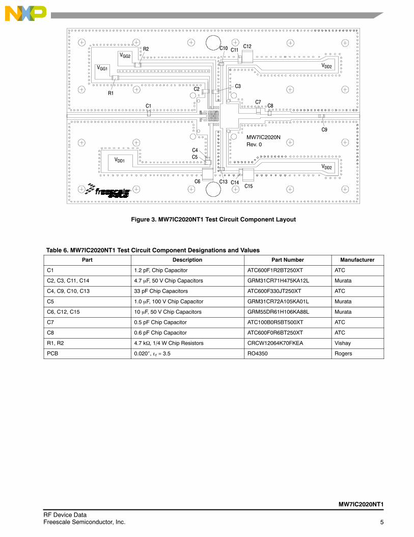
Figure 3. MW7IC2020NT1 Test Circuit Component Layout
MW7IC2020NRev. 0
VGG1
R1
VGG2R2
C1
C2
VDD1
C4C5
C6C15
C14C13
VDD2
C9
C8C7
C3
C12C11C10
VDD2
Table 6. MW7IC2020NT1 Test Circuit Component Designations and Values
Part Description Part Number Manufacturer
C1 1.2 pF, Chip Capacitor ATC600F1R2BT250XT ATC
C2, C3, C11, C14 4.7 F, 50 V Chip Capacitors GRM31CR71H475KA12L Murata
C4, C9, C10, C13 33 pF Chip Capacitors ATC600F330JT250XT ATC
C5 1.0 F, 100 V Chip Capacitor GRM31CR72A105KA01L Murata
C6, C12, C15 10 F, 50 V Chip Capacitors GRM55DR61H106KA88L Murata
C7 0.5 pF Chip Capacitor ATC100B0R5BT500XT ATC
C8 0.6 pF Chip Capacitor ATC600F0R6BT250XT ATC
R1, R2 4.7 k, 1/4 W Chip Resistors CRCW12064K70FKEA Vishay
PCB 0.020, r = 3.5 RO4350 Rogers
6RF Device Data
Freescale Semiconductor, Inc.
MW7IC2020NT1
TYPICAL CHARACTERISTICS
IRL,INPUTRETURNLOSS
(dB)
2060
IRL
Gps
ACPR
f, FREQUENCY (MHz)
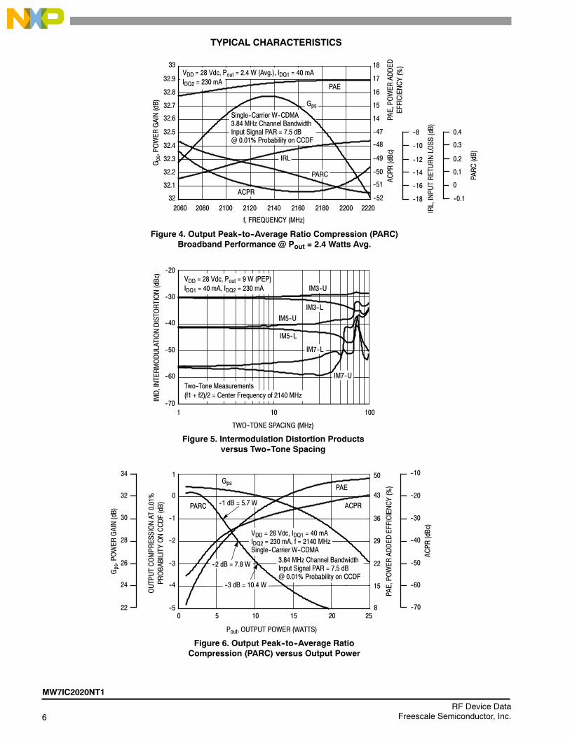
Figure 4. Output Peak--to--Average Ratio Compression (PARC)Broadband Performance @ Pout = 2.4 Watts Avg.
--16
--8
--10
--12
--14
32
33
32.9
32.8
--52
18
17
16
15
--47
--48
--49
--50
PAE,POWER
ADDED
EFFICIENCY(%)
Gps,POWER
GAIN(dB) 32.7
32.6
32.5
32.4
32.3
32.2
2080 2100 2120 2140 2160 2180 2200 2220
14
--51
--18
PARC PARC(dB)
0
0.4
0.3
0.2
0.1
--0.1
ACPR
(dBc)
Single--Carrier W--CDMA3.84 MHz Channel BandwidthInput Signal PAR = 7.5 dB@ 0.01% Probability on CCDF
32.1
VDD = 28 Vdc, Pout = 2.4 W (Avg.), IDQ1 = 40 mAIDQ2 = 230 mA PAE
Figure 5. Intermodulation Distortion Productsversus Two--Tone Spacing
TWO--TONE SPACING (MHz)
10--70
--20
--30
--50
1 100
IMD,INTERMODULATIONDISTORTION(dBc)
--40
IM3--U
IM3--L
IM5--U
IM5--L
IM7--L
IM7--U
VDD = 28 Vdc, Pout = 9 W (PEP)IDQ1 = 40 mA, IDQ2 = 230 mA
--60Two--Tone Measurements(f1 + f2)/2 = Center Frequency of 2140 MHz
Figure 6. Output Peak--to--Average RatioCompression (PARC) versus Output Power
1
Pout, OUTPUT POWER (WATTS)
--1
--3
--55
0
--2
--4
OUTPUTCOMPRESSIONAT
0.01%
PROBABILITY
ONCCDF(dB)
0 10 15 258
50
43
36
29
22
15
PAE,POWER
ADDED
EFFICIENCY(%)
--1 dB = 5.7 W
20
3.84 MHz Channel BandwidthInput Signal PAR = 7.5 dB@ 0.01% Probability on CCDF
ACPRPARC
ACPR
(dBc)
--70
--10
--20
--30
--50
--40
--60
34
Gps,POWER
GAIN(dB)
32
30
28
26
24
22
GpsPAE
VDD = 28 Vdc, IDQ1 = 40 mAIDQ2 = 230 mA, f = 2140 MHzSingle--Carrier W--CDMA
--2 dB = 7.8 W
--3 dB = 10.4 W
MW7IC2020NT1
7RF Device DataFreescale Semiconductor, Inc.
TYPICAL CHARACTERISTICS
1
Gps
ACPR
Pout, OUTPUT POWER (WATTS) AVG.
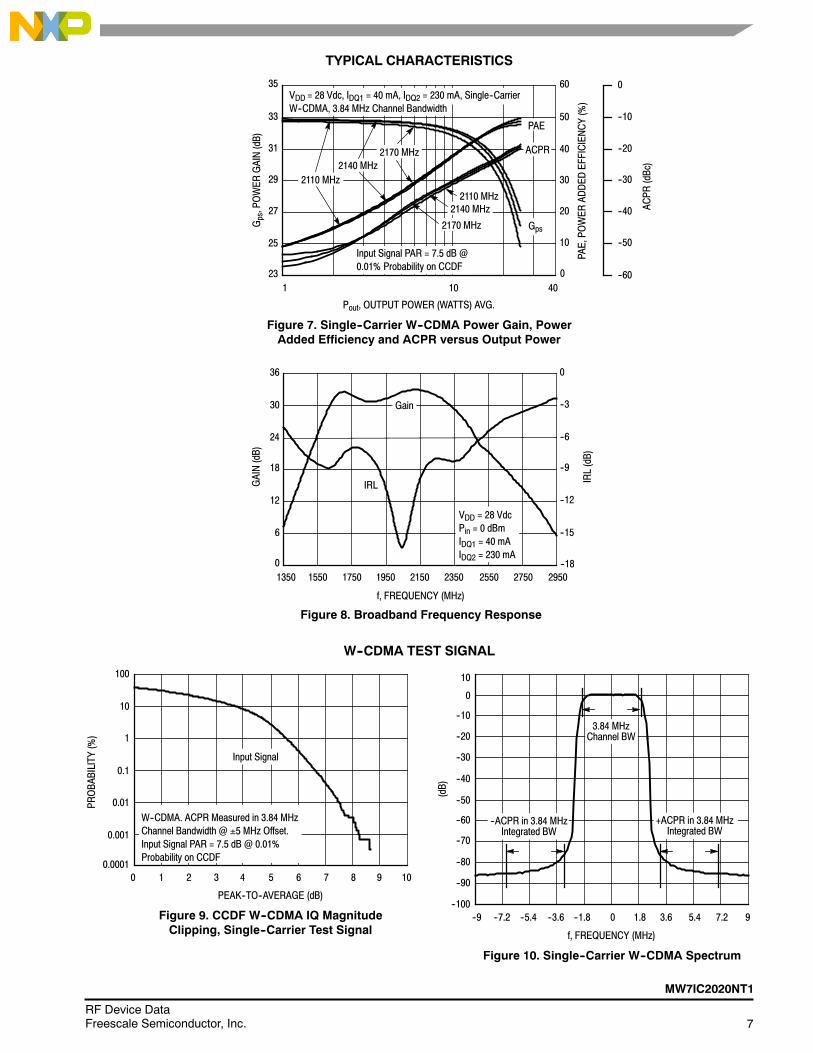
Figure 7. Single--Carrier W--CDMA Power Gain, PowerAdded Efficiency and ACPR versus Output Power
--10
--20
23
35
0
60
50
40
30
20
PAE,POWER
ADDED
EFFICIENCY(%)
Gps,POWER
GAIN(dB)
33
31
10 40
10
--60
ACPR
(dBc)
29
27
25
0
--30
--40
--50
Figure 8. Broadband Frequency Response
0
36
1350
f, FREQUENCY (MHz)
VDD = 28 VdcPin = 0 dBmIDQ1 = 40 mAIDQ2 = 230 mA
24
18
12
1550
GAIN(dB)
30 Gain
1750 1950 2150 2350 2550 2750 2950
IRL
--18
0
--3
--6
--9
--12
IRL(dB)
6 --15
PAE
2170 MHz
2110 MHz2140 MHz
Input Signal PAR = 7.5 dB @0.01% Probability on CCDF
VDD = 28 Vdc, IDQ1 = 40 mA, IDQ2 = 230 mA, Single--CarrierW--CDMA, 3.84 MHz Channel Bandwidth
2110 MHz2140 MHz
2170 MHz
W--CDMA TEST SIGNAL
0.0001
100
0
PEAK--TO--AVERAGE (dB)
Figure 9. CCDF W--CDMA IQ MagnitudeClipping, Single--Carrier Test Signal
10
1
0.1
0.01
0.001
2 4 6 8
PROBABILITY
(%)
W--CDMA. ACPR Measured in 3.84 MHzChannel Bandwidth @ 5 MHz Offset.Input Signal PAR = 7.5 dB @ 0.01%Probability on CCDF
Input Signal
10
--60
--100
10
(dB)
--20
--30
--40
--50
--70
--80
--90
3.84 MHzChannel BW
7.21.8 5.43.60--1.8--3.6--5.4--9 9
f, FREQUENCY (MHz)
Figure 10. Single--Carrier W--CDMA Spectrum
--7.2
--ACPR in 3.84 MHzIntegrated BW
+ACPR in 3.84 MHzIntegrated BW
--10
0
1 3 5 7 9
8RF Device Data
Freescale Semiconductor, Inc.
MW7IC2020NT1
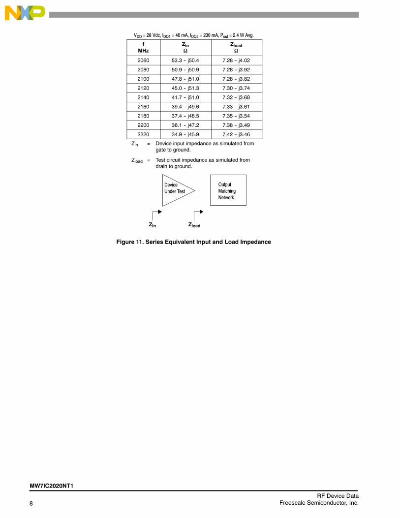
VDD = 28 Vdc, IDQ1 = 40 mA, IDQ2 = 230 mA, Pout = 2.4 W Avg.
fMHz
Zin
Zload
2060 53.3 -- j50.4 7.28 -- j4.02
2080 50.9 -- j50.9 7.28 -- j3.92
2100 47.8 -- j51.0 7.28 -- j3.82
2120 45.0 -- j51.3 7.30 -- j3.74
2140 41.7 -- j51.0 7.32 -- j3.68
2160 39.4 -- j49.6 7.33 -- j3.61
2180 37.4 -- j48.5 7.35 -- j3.54
2200 36.1 -- j47.2 7.38 -- j3.49
2220 34.9 -- j45.9 7.42 -- j3.46
Zin = Device input impedance as simulated fromgate to ground.
Zload = Test circuit impedance as simulated fromdrain to ground.
Figure 11. Series Equivalent Input and Load Impedance
DeviceUnder Test
OutputMatchingNetwork
Zin Zload
MW7IC2020NT1
9RF Device DataFreescale Semiconductor, Inc.
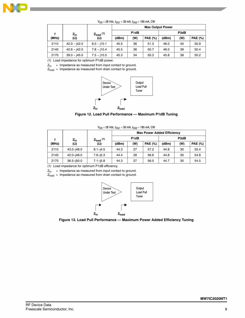
VDD = 28 Vdc, IDQ1 = 30 mA, IDQ2 = 195 mA, CW
f(MHz)
Zin()
Zload (1)
()
Max Output Power
P1dB P3dB
(dBm) (W) PAE (%) (dBm) (W) PAE (%)
2110 42.0 -- j42.0 8.0 -- j10.1 45.5 36 51.3 46.0 40 50.9
2140 42.6 -- j42.0 7.8 -- j10.4 45.5 36 50.7 46.0 39 50.4
2170 39.0 -- j45.0 7.5 -- j10.5 45.3 34 50.3 45.8 38 50.2
(1) Load impedance for optimum P1dB power.
Zin = Impedance as measured from input contact to ground.Zload = Impedance as measured from drain contact to ground.
Figure 12. Load Pull Performance — Maximum P1dB Tuning
DeviceUnder Test
OutputLoad PullTuner
Zin Zload
VDD = 28 Vdc, IDQ1 = 30 mA, IDQ2 = 195 mA, CW
f(MHz)
Zin()
Zload (1)
()
Max Power Added Efficiency
P1dB P3dB
(dBm) (W) PAE (%) (dBm) (W) PAE (%)
2110 43.0--j48.0 8.1--j4.5 44.3 27 57.2 44.8 30 55.4
2140 42.0--j48.0 7.6--j5.3 44.4 28 56.6 44.8 30 54.8
2170 36.5--j50.0 7.1--j5.8 44.3 27 56.0 44.7 30 54.5
(1) Load impedance for optimum P1dB efficiency.
Zin = Impedance as measured from input contact to ground.Zload = Impedance as measured from drain contact to ground.
Figure 13. Load Pull Performance — Maximum Power Added Efficiency Tuning
DeviceUnder Test
OutputLoad PullTuner
Zin Zload
10RF Device Data
Freescale Semiconductor, Inc.
MW7IC2020NT1
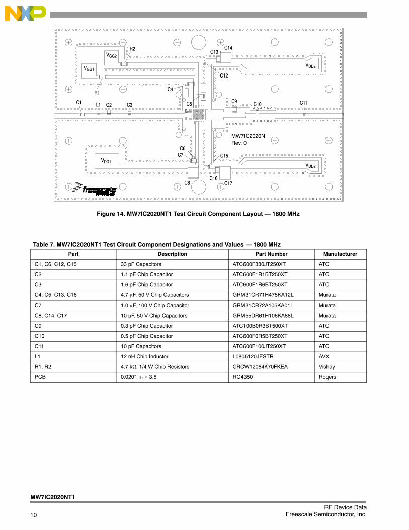
Figure 14. MW7IC2020NT1 Test Circuit Component Layout — 1800 MHz
MW7IC2020NRev. 0
VGG1
VGG2
VDD1VDD2
VDD2
R2
C1
R1
L1 C2 C3
C4
C5
C14C13
C12
C9 C10 C11
C6C7
C8
C15
C16C17
Table 7. MW7IC2020NT1 Test Circuit Component Designations and Values — 1800 MHz
Part Description Part Number Manufacturer
C1, C6, C12, C15 33 pF Capacitors ATC600F330JT250XT ATC
C2 1.1 pF Chip Capacitor ATC600F1R1BT250XT ATC
C3 1.6 pF Chip Capacitor ATC600F1R6BT250XT ATC
C4, C5, C13, C16 4.7 F, 50 V Chip Capacitors GRM31CR71H475KA12L Murata
C7 1.0 F, 100 V Chip Capacitor GRM31CR72A105KA01L Murata
C8, C14, C17 10 F, 50 V Chip Capacitors GRM55DR61H106KA88L Murata
C9 0.3 pF Chip Capacitor ATC100B0R3BT500XT ATC
C10 0.5 pF Chip Capacitor ATC600F0R5BT250XT ATC
C11 10 pF Capacitors ATC600F100JT250XT ATC
L1 12 nH Chip Inductor L0805120JESTR AVX
R1, R2 4.7 k, 1/4 W Chip Resistors CRCW12064K70FKEA Vishay
PCB 0.020, r = 3.5 RO4350 Rogers
MW7IC2020NT1
11RF Device DataFreescale Semiconductor, Inc.
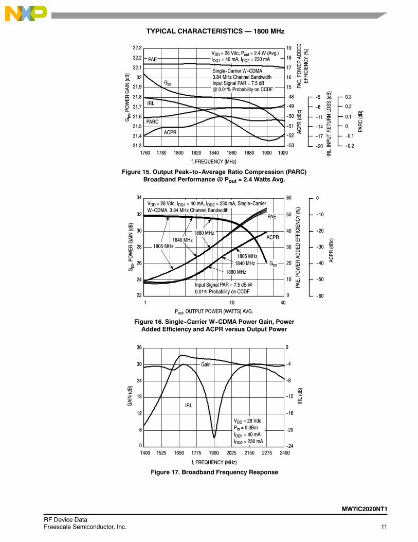
TYPICAL CHARACTERISTICS — 1800 MHz
IRL,INPUTRETURNLOSS
(dB)
1760
IRL
Gps
ACPR
f, FREQUENCY (MHz)
Figure 15. Output Peak--to--Average Ratio Compression (PARC)Broadband Performance @ Pout = 2.4 Watts Avg.
--17
--5
--8
--11
--14
31.3
32.3
32.2
32.1
--53
19
18
17
16
--48
--49
--50
--51
PAE,POWER
ADDED
EFFICIENCY(%)
Gps,POWER
GAIN(dB) 32
31.9
31.8
31.7
31.6
31.5
1780 1800 1820 1840 1860 1880 1900 1920
15
--52
--20
PARC
PARC(dB)
--0.1
0.3
0.2
0.1
0
--0.2
ACPR
(dBc)
Single--Carrier W--CDMA3.84 MHz Channel BandwidthInput Signal PAR = 7.5 dB@ 0.01% Probability on CCDF
31.4
VDD = 28 Vdc, Pout = 2.4 W (Avg.)IDQ1 = 40 mA, IDQ2 = 230 mAPAE
1
Gps
ACPR
Pout, OUTPUT POWER (WATTS) AVG.
Figure 16. Single--Carrier W--CDMA Power Gain, PowerAdded Efficiency and ACPR versus Output Power
--10
--20
22
34
0
60
50
40
30
20
PAE,POWER
ADDED
EFFICIENCY(%)
Gps,POWER
GAIN(dB)
32
30
10 40
10
--60
ACPR
(dBc)
28
26
24
0
--30
--40
--50
PAE
1880 MHz
1805 MHz1840 MHz
Input Signal PAR = 7.5 dB @0.01% Probability on CCDF
VDD = 28 Vdc, IDQ1 = 40 mA, IDQ2 = 230 mA, Single--CarrierW--CDMA, 3.84 MHz Channel Bandwidth
Figure 17. Broadband Frequency Response
0
36
1400
f, FREQUENCY (MHz)
VDD = 28 VdcPin = 0 dBmIDQ1 = 40 mAIDQ2 = 230 mA
24
18
12
1525
GAIN(dB)
30 Gain
1650 1775 1900 2025 2150 2275 2400
IRL
--24
0
--4
--8
--12
--16
IRL(dB)
6 --20
1880 MHz
1840 MHz1805 MHz
12RF Device Data
Freescale Semiconductor, Inc.
MW7IC2020NT1
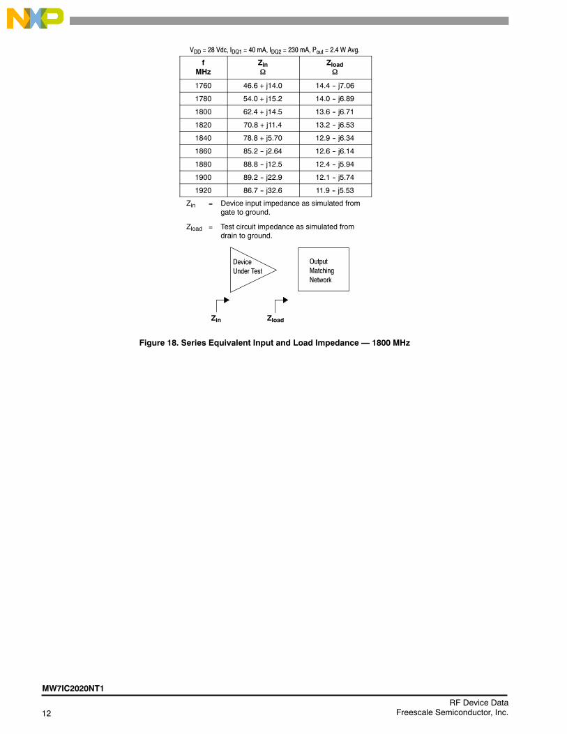
VDD = 28 Vdc, IDQ1 = 40 mA, IDQ2 = 230 mA, Pout = 2.4 W Avg.
fMHz
Zin
Zload
1760 46.6 + j14.0 14.4 -- j7.06
1780 54.0 + j15.2 14.0 -- j6.89
1800 62.4 + j14.5 13.6 -- j6.71
1820 70.8 + j11.4 13.2 -- j6.53
1840 78.8 + j5.70 12.9 -- j6.34
1860 85.2 -- j2.64 12.6 -- j6.14
1880 88.8 -- j12.5 12.4 -- j5.94
1900 89.2 -- j22.9 12.1 -- j5.74
1920 86.7 -- j32.6 11.9 -- j5.53
Zin = Device input impedance as simulated fromgate to ground.
Zload = Test circuit impedance as simulated fromdrain to ground.
Figure 18. Series Equivalent Input and Load Impedance — 1800 MHz
DeviceUnder Test
OutputMatchingNetwork
Zin Zload
MW7IC2020NT1
13RF Device DataFreescale Semiconductor, Inc.
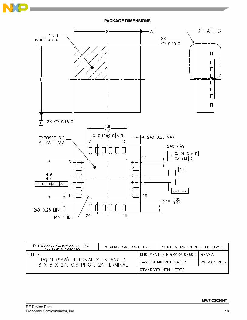
PACKAGE DIMENSIONS
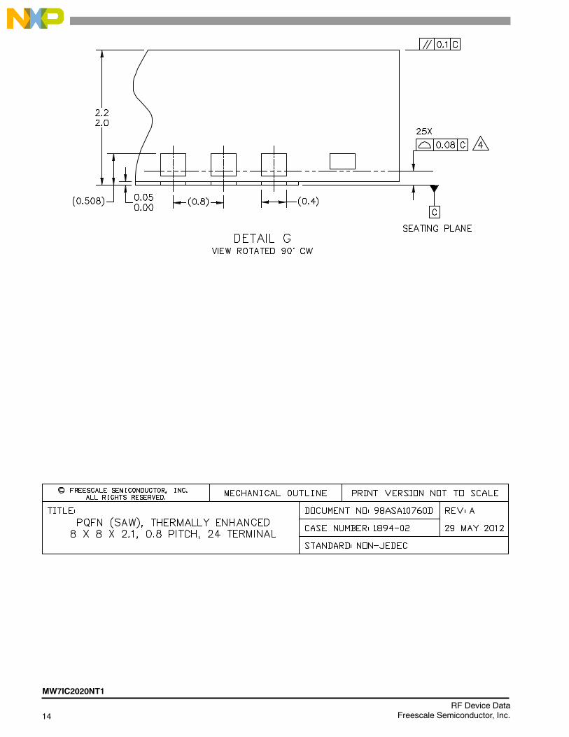
14RF Device Data
Freescale Semiconductor, Inc.
MW7IC2020NT1
MW7IC2020NT1
15RF Device DataFreescale Semiconductor, Inc.
16RF Device Data
Freescale Semiconductor, Inc.
MW7IC2020NT1
PRODUCT DOCUMENTATION, SOFTWARE AND TOOLS
Refer to the following documents, software and tools to aid your design process.
Application Notes AN1955: Thermal Measurement Methodology of RF Power Amplifiers
AN1977: Quiescent Current Thermal Tracking Circuit in the RF Integrated Circuit Family
AN1987: Quiescent Current Control for the RF Integrated Circuit Device Family
Engineering Bulletins EB212: Using Data Sheet Impedances for RF LDMOS Devices
Software Electromigration MTTF Calculator
RF High Power Model
.s2p File
Development Tools Printed Circuit Boards
For Software and Tools, do a Part Number search at http://www.freescale.com, and select the “Part Number” link. Go to theSoftware & Tools tab on the part’s Product Summary page to download the respective tool.
REVISION HISTORY
The following table summarizes revisions to this document.
Revision Date Description
0 Jan. 2012 Initial Release of Data Sheet
1 Dec. 2013 Replaced Case Outline 98ASA10760D, Rev. O with Rev. A, pp. 13--14. Mechanical outline drawingmodified to reflect the correct lead end features. Format of the mechanical outline was also updated to thecurrent Freescale format for Freescale mechanical outlines.
MW7IC2020NT1
17RF Device DataFreescale Semiconductor, Inc.
Information in this document is provided solely to enable system and softwareimplementers to use Freescale products. There are no express or implied copyrightlicenses granted hereunder to design or fabricate any integrated circuits based on theinformation in this document.
Freescale reserves the right to make changes without further notice to any productsherein. Freescale makes no warranty, representation, or guarantee regarding thesuitability of its products for any particular purpose, nor does Freescale assume anyliability arising out of the application or use of any product or circuit, and specificallydisclaims any and all liability, including without limitation consequential or incidentaldamages. “Typical” parameters that may be provided in Freescale data sheets and/orspecifications can and do vary in different applications, and actual performance mayvary over time. All operating parameters, including “typicals,” must be validated foreach customer application by customer’s technical experts. Freescale does not conveyany license under its patent rights nor the rights of others. Freescale sells productspursuant to standard terms and conditions of sale, which can be found at the followingaddress: freescale.com/SalesTermsandConditions.
Freescale and the Freescale logo are trademarks of Freescale Semiconductor, Inc.,Reg. U.S. Pat. & Tm. Off. All other product or service names are the property of theirrespective owners.E 2012--2013 Freescale Semiconductor, Inc.
How to Reach Us:
Home Page:freescale.com
Web Support:freescale.com/support
Document Number: MW7IC2020NRev. 1, 12/2013