Reference Metrology in a Research Fab: The NIST Clean ...
12
Reference Metrology in a Research Fab: The NIST Clean Calibrations Thrust Ronald Dixson 1 *, Joe Fu 1 , Ndubuisi Orji 1 , Thomas Renegar 1 , Alan Zheng 1 , Theodore Vorburger 1 , Al Hilton 1 Marc Cangemi 2 , Lei Chen 2 , Mike Hernandez 2 , Russell Hajdaj 2 , Michael Bishop 3 , Aaron Cordes 4 1 NIST, Precision Engineering Division, 100 Bureau Drive Stop 8212, Gaithersburg, MD 20899 2 NIST, Center for Nanoscale Science and Technology, 100 Bureau Drive, Gaithersburg, MD 20899 3 SEMATECH/ISMI, 2706 Montopolis Drive, Austin, TX 78741 4 SEMATECH/ISMI, 255 Fuller Road, Albany, NY 12203 ABSTRACT In 2004, the National Institute of Standards and Technology (NIST) commissioned the Advanced Measurement Laboratory (AML) – a state-of-the-art, five-wing laboratory complex for leading edge NIST research. The NIST NanoFab – a 1765 m 2 (19 000 ft 2 ) clean room with 743 m 2 (8000 ft 2 ) of class 100 space – is the anchor of this facility and an integral component of the new Center for Nanoscale Science and Technology (CNST) at NIST. Although the CNST/NanoFab is a nanotechnology research facility with a different strategic focus than a current high volume semiconductor fab, metrology tools still play an important role in the nanofabrication research conducted here. Some of the metrology tools available to users of the NanoFab include stylus profiling, scanning electron microscopy (SEM), and atomic force microscopy (AFM). Since 2001, NIST has collaborated with SEMATECH to implement a reference measurement system (RMS) using critical dimension atomic force microscopy (CD-AFM). NIST contributed traceable metrology expertise and SEMATECH provided access to leading edge metrology tools in their facilities. Now, in the newly launched “clean calibrations” thrust at NIST, we are implementing the reference metrology paradigm on several tools in the CNST/NanoFab. Initially, we have focused on calibration, monitoring, and uncertainty analysis for a three-tool set consisting of a stylus profiler, an SEM, and an AFM. Our goal is the development of new and supplemental calibrations and standards that will benefit from the Class 100 environment available in the NanoFab and offering our customers calibration options that do not require exposing their samples to less clean environments. We have completed a preliminary evaluation of the performance of these instruments. The results suggest that the achievable uncertainties are generally consistent with our measurement goals. Keywords: Clean calibrations, AFM, SEM, stylus, step height, magnification, SRM 484, standards, traceability 1. INTRODUCTION In 2004, the National Institute of Standards and Technology (NIST) commissioned the Advanced Measurement Laboratory (AML) – a state-of-the-art, five-wing laboratory complex for leading edge NIST research. The NIST NanoFab – a 1765 m 2 (19 000 ft 2 ) clean room with 743 m 2 (8000 ft 2 ) of class 100 space – is the anchor of this facility and a major facet of the new Center for Nanoscale Science and Technology (CNST) at NIST. Although the CNST/NanoFab is a nanotechnology research facility with a different strategic focus than a current high volume semiconductor fab, metrology tools still play an important role in the nanofabrication research that is conducted here. Some of the metrology tools available to users of the NanoFab include stylus profiling, scanning electron microscopy (SEM), and atomic force microscopy (AFM). For many years, NIST and SEMATECH have worked closely to improve the traceability of dimensional metrology in semiconductor manufacturing. These collaborations have spanned several various measurement technologies including Metrology, Inspection, and Process Control for Microlithography XXIII, edited by John A. Allgair, Christopher J. Raymond Proc. of SPIE Vol. 7272, 727209 · © 2009 SPIE · CCC code: 0277-786X/09/$18 · doi: 10.1117/12.815499 Proc. of SPIE Vol. 7272 727209-1
Transcript of Reference Metrology in a Research Fab: The NIST Clean ...
Reference Metrology in a Research Fab: The NIST Clean Calibrations Thrust
Ronald Dixson1*, Joe Fu1, Ndubuisi Orji1, Thomas Renegar1, Alan Zheng1, Theodore Vorburger1, Al Hilton1
Marc Cangemi2, Lei Chen2, Mike Hernandez2, Russell Hajdaj2, Michael Bishop3, Aaron Cordes4 1NIST, Precision Engineering Division, 100 Bureau Drive Stop 8212, Gaithersburg, MD 20899
2NIST, Center for Nanoscale Science and Technology, 100 Bureau Drive, Gaithersburg, MD 20899 3SEMATECH/ISMI, 2706 Montopolis Drive, Austin, TX 78741
4SEMATECH/ISMI, 255 Fuller Road, Albany, NY 12203
ABSTRACT
In 2004, the National Institute of Standards and Technology (NIST) commissioned the Advanced Measurement Laboratory (AML) – a state-of-the-art, five-wing laboratory complex for leading edge NIST research. The NIST NanoFab – a 1765 m2 (19 000 ft2) clean room with 743 m2 (8000 ft2) of class 100 space – is the anchor of this facility and an integral component of the new Center for Nanoscale Science and Technology (CNST) at NIST. Although the CNST/NanoFab is a nanotechnology research facility with a different strategic focus than a current high volume semiconductor fab, metrology tools still play an important role in the nanofabrication research conducted here. Some of the metrology tools available to users of the NanoFab include stylus profiling, scanning electron microscopy (SEM), and atomic force microscopy (AFM). Since 2001, NIST has collaborated with SEMATECH to implement a reference measurement system (RMS) using critical dimension atomic force microscopy (CD-AFM). NIST contributed traceable metrology expertise and SEMATECH provided access to leading edge metrology tools in their facilities. Now, in the newly launched “clean calibrations” thrust at NIST, we are implementing the reference metrology paradigm on several tools in the CNST/NanoFab. Initially, we have focused on calibration, monitoring, and uncertainty analysis for a three-tool set consisting of a stylus profiler, an SEM, and an AFM. Our goal is the development of new and supplemental calibrations and standards that will benefit from the Class 100 environment available in the NanoFab and offering our customers calibration options that do not require exposing their samples to less clean environments. We have completed a preliminary evaluation of the performance of these instruments. The results suggest that the achievable uncertainties are generally consistent with our measurement goals. Keywords: Clean calibrations, AFM, SEM, stylus, step height, magnification, SRM 484, standards, traceability
1. INTRODUCTION In 2004, the National Institute of Standards and Technology (NIST) commissioned the Advanced Measurement Laboratory (AML) – a state-of-the-art, five-wing laboratory complex for leading edge NIST research. The NIST NanoFab – a 1765 m2 (19 000 ft2) clean room with 743 m2 (8000 ft2) of class 100 space – is the anchor of this facility and a major facet of the new Center for Nanoscale Science and Technology (CNST) at NIST. Although the CNST/NanoFab is a nanotechnology research facility with a different strategic focus than a current high volume semiconductor fab, metrology tools still play an important role in the nanofabrication research that is conducted here. Some of the metrology tools available to users of the NanoFab include stylus profiling, scanning electron microscopy (SEM), and atomic force microscopy (AFM). For many years, NIST and SEMATECH have worked closely to improve the traceability of dimensional metrology in semiconductor manufacturing. These collaborations have spanned several various measurement technologies including
Metrology, Inspection, and Process Control for Microlithography XXIII, edited by John A. Allgair, Christopher J. RaymondProc. of SPIE Vol. 7272, 727209 · © 2009 SPIE · CCC code: 0277-786X/09/$18 · doi: 10.1117/12.815499
Proc. of SPIE Vol. 7272 727209-1

CD-AFM and CD-SEM. The implementation of traceable CD-AFM reference metrology has been a major component of this collaboration.1-5 SEM modeling and data interpretation has been another.6-8 Now, with a newly launched “clean calibrations” thrust at NIST, we are implementing the reference metrology paradigm on several tools in the CNST/NanoFab. Initially, we are focusing on calibration, monitoring, and uncertainty analysis for a three-tool set consisting of a stylus profiler, an SEM, and an AFM. Our larger goal is the development of new and supplemental calibrations and standards that will benefit from the environment available in the NanoFab and offer our customers calibration options that do not require exposing their samples to less clean environments. In this paper, we will describe the approach and status of the clean calibrations thrust.
2. PERFORMANCE OF INSTRUMENTS 2.1 Stylus Profiler The stylus profiler used in the clean calibrations project has a nominal 0.1 nm vertical resolution when using the lowest range setting of 6.5 µm. It employs a scanning stage design and can accommodate sample sizes up to 150 mm wafers. Step heights of up to 262 µm can be measured using this instrument, and the available lateral scan range is from 50 µm up to 30 mm. The profiler is typically operated using one of two diamond styli with radii of either 0.7 μm or 2.5 μm. In Fig. 1 some preliminary performance data are shown using 90 nm and 300 nm NIST-internal step height masters used in our current stylus profiler calibration facility.
Stylus Profiler: Performance Monitoring
0
0.5
1
1.5
2
2.5
3
3.5
1 2 3 4 5 6
Session
Cal
Err
or (%
)
0
0.5
1
1.5
2
2.5
Rep
eata
bilit
y (n
m) Out of cal' percent Cal-spike
Out of cal' percent Initial
Repeatability (1 SD*) - 300 nmstepRepeatability (1 SD*) - 90 nmstep
Figure 1. Performance data on the stylus profiler. Typical scale calibration bias ranges from 1 % to 2 %. Observed repeatability on the 90 nm and 300 nm master standards has been improved relative to the initial observations, but still lags the performance of the profiler in our current calibration facility. The dashed reference line represents the performance of one of our calibration tools on the 300 nm master – which exhibited a one standard deviation (SD) repeatability of 0.06 nm. NIST has considerable experience in stylus profiling and a long standing program in dimensional metrology using profilers.9 Currently, most traceable step height measurements performed by NIST are carried out using stylus profilers.
Proc. of SPIE Vol. 7272 727209-2

Mag = 2.21 K X EHT = 10.00 kV Signal A = InLens Date :6 Feb 2009
Tilt Angle = 0.0 WD = 4.0 rrrr Signal B = InLens Tine :9:20:43 cjS&T*gy
These profilers do not have intrinsic scale calibration and thus function as comparators. Master step height standards ranging from 29 nm to 152 μm are used to calibrate the profilers. These master standards were calibrated primarily using interferometric methods. As part of an ongoing effort to validate and refine its uncertainty budgets for stylus profiler metrology, NIST has participated in several international comparisons of step height measurements among the metrology institutes of various nations.10-12 We have also performed an internal comparison of step height metrology between our calibrated profilers and other instruments capable of traceable metrology – including an AFM discussed in Sec. 2.3.13-15 It was possible to use the AFM measurements to improve the calibration on one of the 90 nm master steps used in the profiler facility.15 This standard and the 300 nm master were used for the evaluation of the NanoFab profiler. The preliminary observations in Fig. 1 indicate that performance of this profiler lags the performance of the profilers in our calibration facility. The typical initial scale calibration bias observed over several months ranged from 1 % to 2 %. The reproducibility (one standard deviation) of step height measurements on the 90 nm and 300 nm master standards ranged up to 2 nm. This variation is larger than that typically observed in our calibration facility as represented by the reference line in Fig. 1. We suspect that environmental effects could be partially responsible for this relative differential in performance, and the apparent improvement seen in Fig. 1 could be the result of improved vibration isolation and some preventive maintenance that was performed – including cleaning the reference block for the profiling stage. 2.2 Scanning Electron Microscope The SEM used in this work is a field emission (FE) SEM. This tool is capable of imaging structures down to ≤ 10 nm dimensions and can accommodate sample sizes up to 200 mm wafers. It is equipped with both secondary and backscattered detectors, has a magnification range from 12X to 900kX, and can achieve 1.0 nm imaging resolution at 15 keV.
Indentation forNavigation
500 nm intervals
Indentation forNavigation
500 nm intervals
Figure 2. An image of an SRM 484 control sample obtained using the FE-SEM. The available pitches, which range from 500 nm to 5 μm, are visible – as well as the indentation mark used for alignment with the calibrated area. NIST has considerable experience in SEM dimensional metrology and previously developed a Standard Reference Material (SRM) for SEM magnification calibration16,17 – SRM 484 – an SEM image of which is shown in Fig. 2. This
Proc. of SPIE Vol. 7272 727209-3

I in Mag = 400 KX EHT = 000 kV SgnoIA= InLen Date :18 Sep 2008 C '451HH Tdt Angle = 0,0 WD= 5 rrnn Signel B = InLenn Time :15:48:25
standard was calibrated using an instrument known as the metrology electron microscope (MEM), which incorporated an interferometric displacement stage for traceability.18 It was used for calibration of approximately 800 units of SRM 484 and was decommissioned in 2003 after more than two decades of operation. In addition to SRM 484, NIST has an active project in development of SEM magnification standards for the semiconductor industry, and released a Reference Material (RM) 8090, on lithographically patterned silicon chips.19,20 The patterns have non-traceable pitch values ranging down to 200 nm. Both SRM 484 and RM 8090 are currently out of stock. A second generation Si chip sample, RM 8820, will be released soon.§ The close cooperation between NIST and SEMATECH has now extended into the clean calibrations thrust. For several years, SEMATECH/ISMI has been using an FEI IC3D† analysis workstation for off line analysis of SEM images. An illustration of this software tool as applied to an image of SRM 484 is shown in Fig. 3.
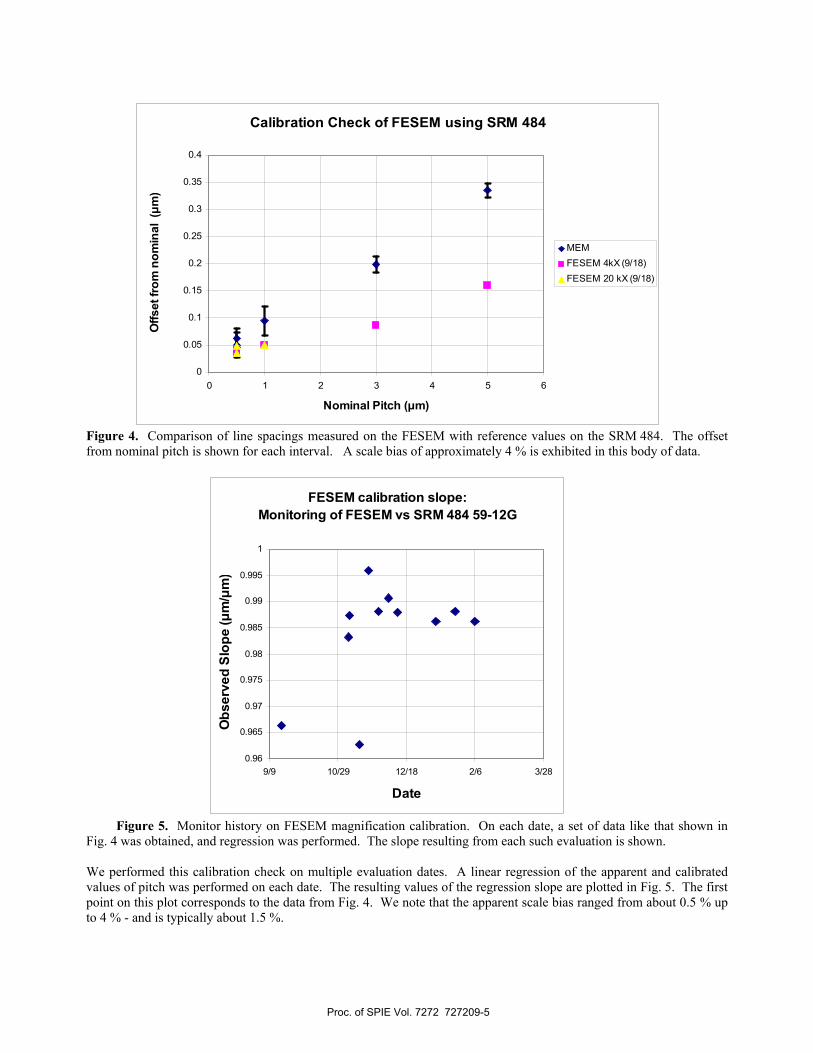
Figure 3. Illustration of the image analysis performed using an FEI/IC3D† analysis workstation at ISMI/SEMATECH. The green boxes represent the boundaries within which the software locates the position of the feature. Over a period of several months, we have been monitoring the performance of the SEM using an SRM 484 control sample. The available line spacings on this sample range from 500 nm to 5 μm. The magnification calibration of the SEM was checked against the reference values on SRM 484 – as originally measured with the MEM. An example of this comparison is shown in Fig. 4. The plot in Fig. 4 shows the offset from the nominal spacing for each interval. Note that the error bars shown on the MEM results represent the original expanded uncertainties, which correspond approximately to 95 % confidence intervals. The expression of uncertainty in NIST measurements, including coverage factors, is discussed more in Sec. 3.1. A scale bias of approximately 4 % is observed in these results. § Reference Material (RM) 8820 will be available through the Standard Reference Materials Program of the NIST Measurement Services Division (MSD). The on-line catalogue can be accessed at https://www-s.nist.gov/srmors/ . †Certain commercial equipment is identified in this paper to adequately describe the experimental procedure. Such identification does not imply recommendation or endorsement by the National Institute of Standards and Technology nor does it imply that the equipment identified is necessarily the best available for the purpose.
Proc. of SPIE Vol. 7272 727209-4
Calibration Check of FESEM using SRM 484
0
0.05
0.1
0.15
0.2
0.25
0.3
0.35
0.4
0 1 2 3 4 5 6
Nominal Pitch (μm)
Offs
et fr
om n
omin
al (μm
)
MEMFESEM 4kX (9/18)FESEM 20 kX (9/18)
Figure 4. Comparison of line spacings measured on the FESEM with reference values on the SRM 484. The offset from nominal pitch is shown for each interval. A scale bias of approximately 4 % is exhibited in this body of data.
FESEM calibration slope:Monitoring of FESEM vs SRM 484 59-12G
0.96
0.965
0.97
0.975
0.98
0.985
0.99
0.995
1
9/9 10/29 12/18 2/6 3/28
Date
Obs
erve
d Sl
ope
(μm
/μm
)
Figure 5. Monitor history on FESEM magnification calibration. On each date, a set of data like that shown in Fig. 4 was obtained, and regression was performed. The slope resulting from each such evaluation is shown. We performed this calibration check on multiple evaluation dates. A linear regression of the apparent and calibrated values of pitch was performed on each date. The resulting values of the regression slope are plotted in Fig. 5. The first point on this plot corresponds to the data from Fig. 4. We note that the apparent scale bias ranged from about 0.5 % up to 4 % - and is typically about 1.5 %.
Proc. of SPIE Vol. 7272 727209-5

2.3 Atomic Force Microscope The AFM used in this work is a conventional or one-dimensional (1D) AFM. It is capable of operating in a variety of contrast modes, and it can accommodate sample sizes up to 150 mm wafers. It has a 90 µm lateral scan range and a vertical range of approximately 7 µm. NIST has considerable experience in AFM dimensional metrology using both conventional tools and CD-AFM.1-5, 13-15 One component of the NIST program is the calibrated atomic force microscope (C-AFM) – a custom built instrument constructed at NIST for traceable dimensional metrology. The design, performance, and uncertainties of the system have been previously described.13-15 The C-AFM has metrology traceability via the 633 nm wavelength of the I2-stabilized He-Ne laser (a recommended radiation for the realization of the meter in the visible wavelength range) for all three axes, and this is accomplished using heterodyne laser interferometers. The C-AFM is capable of performing both traceable pitch and step height measurements, and it has been used by NIST to perform both types of measurements for external customers. Additionally, we have participated in several international comparisons among the metrology institutes of various nations. The measurands studied in these comparisons were pitch (both one and two dimensional) and step height.12, 21-22 The step height comparison, known as NANO2, was completed in 2003.12 Five samples, having nominal step heights of 7 nm, 20 nm, 70 nm, 300 nm, and 800 nm, were used for this comparison. In addition to the circulated set of standards, each laboratory received supplemental sets to be retained as internal masters. We have been using one of these sets at NIST for z-axis calibration and monitoring of the AFM in the NanoFab, and some of these results are shown in Fig. 6 and Fig. 7.
Z-axisScale Calibration and non-linearityassessment on AFM01
y = 1.0047xR2 = 1
0
100
200
300
400
500
600
700
800
900
0 100 200 300 400 500 600 700 800 900
C-AFM Reference Height (nm)
AFM
01 M
easu
red
Hei
ght (
nm)
Figure 6. Ordinary regression of apparent step heights measured on the NanoFab AFM (known by the identifier AFM01) versus the reference values from measurements taken on the NIST C-AFM. The slope indicates a vertical scale bias of approximately 0.5 %.
Proc. of SPIE Vol. 7272 727209-6

Our initial goal with the AFM is to perform traceable step height measurements in the clean room environment of the NanoFab. As the regression slope in Fig. 6 illustrates, the typical z-axis scale bias we have observed is approximately 0.5 %. Our preliminary observations suggest that the reproducibility of this scale bias is at least a factor of three lower than this level – suggesting that we should be able to maintain a traceable scale calibration with approximately a 0.2 % standard uncertainty. Some indication of this can be inferred from Fig. 7, from which the level of non-linearity can also be estimated. Figure 7 shows the percentage deviation of the AFM01 apparent step height results relative to the C-AFM reference values for each of the five measured step heights – with data taken on multiple evaluation dates. Note that the signs are all positive due to the vertical scale bias, and the larger apparent deviations at small height values are due to a scanner artifact that is discussed more below. Over the period of these observations, the results on the nominal 800 nm and 300 nm step heights – which have actual values of 780 nm and 290 nm, respectively – indicate that the reproducibility of percent scale bias is 0.2 %. This is estimated from the standard deviation of the percent biases in both sets of results. Note also that the average biases observed for these two step heights – 0.7 % for the nominal 300 nm height and 0.4 % for the nominal 800 nm height – are statistically consistent with the regression estimate of 0.5 %. The agreement between the observations for the two heights also suggests non-linearity well below the official vendor spec of 1 %.
Z-axis Scale Calibration and non-linearityassessment on AFM01
0
2
4
6
8
10
12
14
779.7 290.4 67.4 20.1 6.6
C-AFM Reference Height (nm)
% D
evia
tion
from
refe
renc
e va
lue
Day 1Day 2Day 12Day 19Day 26Day 39
Vendor specon non-linearity
Large apparentvalues probably dueto scanner artifacts.
Z-axis Scale Calibration and non-linearityassessment on AFM01
0
2
4
6
8
10
12
14
779.7 290.4 67.4 20.1 6.6
C-AFM Reference Height (nm)
% D
evia
tion
from
refe
renc
e va
lue
Day 1Day 2Day 12Day 19Day 26Day 39
Vendor specon non-linearity
Large apparentvalues probably dueto scanner artifacts.
Figure 7. Plot of percentage deviation of AFM01 results from C-AFM reference values for the five measured step heights over a period of more than one month. The signs are all positive due to the scale bias, and the larger apparent deviations at small height values are due to scanner artifacts. The larger deviations seen in Fig. 7 for the nominal 70 nm, 20 nm, and 7 nm step heights are believed to be primarily due to the residual effect of scanner bow. The AFM employs a tube scanner for motion generation, but also features closed loop control using optical-lever-arm displacement sensors.23† This design allows the scanner to have a large lateral scan range and good linearization, but the head does still exhibit some classical artifacts of tube scanners – such as bow.24 Scanner bow is a consequence of the arc like motion of the tube scanner – the end of which essentially swings as a pendulum. This means that if a perfectly flat sample were scanned in the instrument, the apparent surface would resemble an inverted bowl. The design of the head is such that this artifact is relatively small: The deviations from planarity are only about 15 nm toward the edges of the lateral scan range. However, since the calibration standards we
Proc. of SPIE Vol. 7272 727209-7

0
2 nm
0 70 jtrn
35 nm
a
N0 70 trn
900 nm
0
900 nm
00 10pm
I/IN
0 /0pm
0 7ojim
50 nm
0 iom 0
35 nrn
0
are using require approximately an 85 µm lateral scan, the impact of scanner bow on our measurements is not negligible. This is illustrated in Fig. 8 with a comparison of scan lines from the C-AFM and AFM01.
Figure 8. Illustration of scanner performance with line scans from the C-AFM (left) on the 7 nm step height and from the NanoFab AFM (right) on the 20 nm step height. Both profiles are from the raw image. Over the lateral range of 90 μm, the C-AFM scanner exhibits flatness of 1 nm while the AFM01 scanner exhibits approximately 15 nm of out-of-plane deviation.
Figure 9. Illustration of basic scanner bow correction method for scan lines on nominal 800 nm (left) and 7 nm (right) step heights. The raw profiles are shown on top, and the corrected ones on the bottom. The correction method is to fit a parabola to the wings of the profile. Although this removes most of the bow, the scan line on the small step reveals small residual artifacts that have a much larger percentage effect on the step height calculation for the smaller step heights.
Proc. of SPIE Vol. 7272 727209-8

The correction of scanner bow in data processing has been the subject of previous investigations by others.25-26 In Fig. 9, we illustrate an elementary correction method that we used for analysis of our preliminary data. Our method was to fit a parabola to the wings of the profile (excluding the step height region in the middle) – and then to subtract this parabola to remove the scanner bow prior to the step height calculation. As Fig. 9 shows, this relatively simple correction strategy generally works well. For the smaller steps, however, the small remaining edge effects and top surface distortion are not negligible compared to the magnitude of the step height. Consequently, the percentage biases that were shown in Fig. 7 are larger for these steps. For future work, we are considering the possibility of implementing a more elaborate scanner bow correction methodology developed by Edwards, et al.26 This method involves the simultaneous fitting of both a polynomial and a step function to the scan lines. This would have the advantage of using more of the available data, and the residual impact of scanner bow on the apparent step heights is expected to be much smaller.
3. IMPLICATIONS AND FUTURE PLANS
3.1 Uncertainties In general, the approach27 to uncertainty budgets adopted by NIST28 is to develop an estimated contribution for every known source of uncertainty in a given measurement and to include terms pertaining to both the instrument used and the particular specimen measured. Terms evaluated exclusively by statistical methods are known as Type A evaluations. Other terms, known as Type B evaluations, are evaluated using some combination of measured data, physical models, or assumptions about the probability distribution. All of these terms are then added in quadrature to obtain a combined standard uncertainty for the measurement. This is usually multiplied by a coverage factor k to obtain a combined expanded uncertainty.28 The most common coverage factor used is k = 2, which would correspond to approximately a 95 % confidence interval for a normal (Gaussian) distribution. In our previous work with the C-AFM, stylus tools, SEM, and CD-AFM, we have developed uncertainty budgets for relevant measurands.1-5,9,13-15,17 Our intent is to develop similar uncertainty budgets for measurements using the tools involved in the clean calibrations thrust. The limit on achievable step height uncertainty using the stylus profiler is not yet known, but our early results suggest that it wouldn’t be larger than the quadrature sum of 1.0 nm and 1 % of the measured height. Although this level of uncertainty may be suitable for some users of the NanoFab, it may not be sufficient for some potential customers of the clean calibrations thrust. We are considering further upgrades to the environmental isolation of the current tool, and we may also explore the possibility of acquiring a newer generation profiler. There are many challenging sources of uncertainty in performing SEM based dimensional metrology.29 This is particularly true for measurands such as linewidth. The uncertainty of SEM pitch measurements is primarily dependent on the accuracy of the magnification calibration. Therefore, the measurement of a known pitch standard is the most straightforward method to calibrate the magnification. Unfortunately, the magnification of an SEM is dependent upon a variety of instrumental, environmental, and even sample-related parameters which may not be fully reproducible, or may have hysteresis, even at nominally equivalent operating conditions. Consequently, the scope of applicability of an SEM uncertainty estimate may be somewhat restricted. Our observations using the SEM show the effective magnification to be consistently lower than nominal – ranging from 0.5 % to 4 % – all taken under imaging conditions we believed to be equivalent. The distribution of the observations appears to suggest a dependence on factors that we are not controlling in our measurement runs. The most optimistic interpretation of the results shown in Fig. 5 would be that we can calibrate the magnification to a standard uncertainty of approximately 0.5 % percent, but this is probably too optimistic. A pessimistic limit would be
Proc. of SPIE Vol. 7272 727209-9

that we can only calibrate it to 4 %. At the present, we regard 2 % as a reasonable working estimate of a standard uncertainty that we could achieve with this tool. The most recent release of SRM 484 had a smallest interval of 500 nm with an expanded uncertainty (k = 2) of 20 nm. One possible goal of the clean calibrations thrust is to continue the SRM 484 series by using the FESEM as a comparator between the original control samples and the new ones. The pessimistic estimate of scale uncertainty is too large to perform these measurements without an unacceptable increase in uncertainty. The optimistic limit, however, would readily support this objective. Due to the non-wafer form of the SRM 484 specimen and its material composition – alternating layers of Au and Ni – this standard may not be appropriate for use in some contemporary SEMs. For the in-line CD-SEMs used in semiconductor manufacturing metrology, difficulties may arise due to a combination of the low accelerating voltages, the ferro-magnetism of the standard itself, and in-lens detectors that are commonly used in such instruments.19 Consequently, for both instrumental and application reasons, we do not yet know if it will be appropriate to calibrate a new release of SRM 484. This possibility is still under consideration. In AFM based dimensional metrology, the most challenging sources of uncertainty are usually related to the effect of the AFM tip and its interaction with the measured surface.30 This means that linewidth and roughness are particularly challenging measurands. Pitch and step height measurements, however, have much less dependence on tip-related effects and are largely dependent upon the accuracy of the scanner displacement metrology. The initial focus of the clean calibrations effort with respect to AFM metrology is on step height, and our preliminary results suggest that a z-axis scale calibration standard uncertainty of 0.2 % may be achievable. However, to develop a comprehensive uncertainty budget, we need to perform a more thorough evaluation of the z-axis non-linearity and implement a more sophisticated method of correcting for the scanner bow. If a standard uncertainty of 0.2 % or below can be readily achieved with this tool, then performance would be on par with what we have achieved working with other commercially available instruments.
4. SUMMARY In 2004, NIST commissioned the AML – a state-of-the-art, five-wing laboratory complex for leading edge NIST research. The NanoFab – a 1765 m2 (19 000 ft2) clean room with 743 m2 (8000 ft2) of class 100 space – is the anchor of this facility and a major facet of the new CNST at NIST. Metrology tools available to users of the NanoFab include stylus profiling, SEM, and AFM. In the newly launched “clean calibrations” thrust at NIST, we are working with these tools to implement a reference metrology paradigm on multi-tool platform within the CNST/NanoFab. Toward this end, we have completed a preliminary evaluation of the performance of these instruments. Our ultimate goal is the development of new and supplemental calibrations and standards that will benefit from the environment available in the NanoFab and offer our customers calibration options that don’t require exposing their samples to less clean environments. The results of our preliminary tool evaluations suggest that the achievable uncertainties are generally consistent with our measurement goals. ACKNOWLEDGEMENTS This work was performed in part at the Center for Nanoscale Science and Technology (CNST) NanoFab at the National Institute of Standards and Technology, and was jointly supported at NIST by the CNST, the NIST Office of Microelectronics Programs (OMP), and the Nanomanufacturing Program in the NIST Manufacturing Engineering Laboratory (MEL). We also thank Robert J. Celotta, Jack Martinez, Yaw Obeng, and Richard M. Silver of NIST for their encouragement and support of this work.
Proc. of SPIE Vol. 7272 727209-10

*Address all correspondence to Ronald Dixson at [email protected] †Certain commercial equipment is identified in this paper to adequately describe the experimental procedure. Such identification does not imply recommendation or endorsement by the National Institute of Standards and Technology nor does it imply that the equipment identified is necessarily the best available for the purpose.
REFERENCES 1. N. G. Orji, R. G. Dixson, A. Martinez, B. D. Bunday, J. A. Allgair, and T. V. Vorburger, “Progress on
implementation of a reference measurement system based on a critical-dimension atomic force microscope,” J. Micro/Nanolith. MEMS MOEMS Vol. 6, 023002-1-10 (2007).
2. R. Dixson, J. Fu, N. Orji, W. Guthrie, R. Allen, M. Cresswell, “CD-AFM Reference Metrology at NIST and
SEMATECH”, SPIE Proceedings Vol. 5752, 324-336 (2005). 3. R. Dixson, A. Guerry, "Reference Metrology using a Next Generation CD-AFM", SPIE Proceedings Vol. 5375,
633-646 (2004). 4. R. Dixson, A. Guerry, M. Bennett, T. Vorburger, B. Bunday, “Implementation of a Reference Measurement System
using CD-AFM,” SPIE Proceedings Vol. 5038, 150-165 (2003). 5. R. Dixson, A. Guerry, M. Bennett, T. Vorburger, M. Postek, “Toward Traceability for At Line AFM Dimensional
Metrology,” SPIE Proceedings Vol. 4689, 313-335 (2002). 6. J. S. Villarrubia, A. Vladar, B. Bunday, M. Bishop, “Dimensional Metrology of Resist Lines using a SEM model-
based library approach,” SPIE Proceedings Vol. 5375, 199-209 (2004). 7. J. S. Villarrubia, B. Bunday, “Unbiased estimation of linewidth roughness,” SPIE Proceedings Vol. 5752, 480-488
(2005). 8. R. Katz, C. D. Chase, R. Kris, R. Peltinov, J. Villarrubia, B. Bunday, “Bias reduction in roughness measurement
through SEM noise removal,” SPIE Proceedings Vol. 6152, 61524L (2006). 9. J. F. Song and T. V. Vorburger, “Standard Reference Specimens in Quality Control of Engineering Surfaces,”
J. Res. Natl. Inst. Stand. Technol. 96, 271 (1991). 10. K. Doytchinov, F. Kornblit, C. Colin, J. C. V. Oliveira, T. B. Renegar, T. V. Vorburger, "International Comparison
of Surface Roughness and Step Height (Depth) Standards, SIML-S2 (SIM 4.8)," Metrologia, Vol. 43, 04002 (2006).
11. H. Haitjema, “International comparison of depth-setting standards,” Metrologia, Vol. 34, 161-167 (1997). 12. L Koenders, et al. “Comparison on Nanometrology: Nano 2—Step height” Metrologia 40, No 1A (Technical
Supplement 04001) (2003). 13. R. Dixson, R. Köning, T. V. Vorburger, J. Fu, V. W. Tsai, “Measurement of pitch and width samples with the NIST
calibrated atomic force microscope,” SPIE Proceedings Vol. 3332, 420-432 (1998). 14. R. Dixson, R. Köning, V.W. Tsai, J. Fu, T.V. Vorburger, “Dimensional Metrology with the NIST calibrated atomic
force microscope,” SPIE Proceedings Vol. 3677, 20-34 (1999).
Proc. of SPIE Vol. 7272 727209-11
15. R. Dixson, R. Köning, J. Fu, T. Vorburger, B. Renegar, “Accurate Dimensional Metrology with Atomic Force Microscopy,” SPIE Proceedings Vol. 3998, 362-368 (2000).
16. J. Fu, M. C. Croarkin, T. V. Vorburger, “The measurement and uncertainty of a calibration standard for the
scanning electron microscope,” J. Res. Natl. Inst. Stand. Technol. 99, p.191 (1994). 17. J. Fu, T. Vorburger, “The Calibration of Scanning Electron Microscope Magnification Standards SRM484,”
SPIE Proceedings Vol. 2725, pp. 608-614 (1996). 18. G. G. Hembree, S. W. Jensen, J. F. Marchiando, “Submicrometer linewidth measurement by electron microscopy,”
Proceedings of 38th Annual Electron Microscopy Society of America, G. W. Bailey, editor, p. 312 (1980). 19. M. Postek, “Scanning Electron Microscope Based Metrological Electron Microscope System and New Prototype
Scanning Electron Microscope Magnification Standard,” Scanning Microscopy, Vol. 3, 1087-1099 (1989). 20. B. Newell, M. Postek, J. Van der Ziel, “Fabrication Issues for the Prototype NIST SRM 2090a SEM Magnification
Calibration Standard,” J. Vac. Sci. Technol. B, Vol. 93, 2671-2675 (1995). 21. F. Meli, “International comparison in the field of nanometrology: pitch of 1D gratings (Nano4),” Proceedings of
the 2nd Euspen (European Society for Precision Engineering) International Conference, held in Turin, Italy, May 27-31, 2001, 358-361, (2001).
22. Joergen Garnaes, Kai Dirscherl, “NANO5-2D Grating-Final Report,” Metrologia, Vol. 45, 04003 (2008). 23. Dimension Hybrid XYZ Scanning Probe Microscope Head, Veeco Support Note 394, Rev. B (2004). 24. J. E. Griffith, D. A. Grigg, “Dimensional metrology with scanning probe microscopes,” J. Appl. Phys., Vol. 74,
R83-R109 (1993). 25. H. Edwards, “New method to estimate step heights in scanning-probe microscope images,” Nanotechnology,
Vol. 8, 6-9 (1997). 26. H. Edwards, R. McGlothlin, Elisa U, “Vertical metrology using scanning-probe microscopes: Imaging distortions
and measurement repeatability,” J. Appl. Phys., Vol. 83, 3952-3971 (1998). 27. Guide to the Expression of Uncertainty in Measurement, International Organization for Standardization, Geneva
(1995). 28. B. N. Taylor and C. E. Kuyatt, Guidelines for Evaluating and Expressing the Uncertainty of NIST Measurement
Results, NIST Tech. Note 1297, (1994). 29. M. T. Postek, A. E. Vladar, Samuel N. Jones, and William J. Keery, “Interlaboratory Study on the Lithographically
Produced Scanning Electron Microscope Magnification Standard Prototype,” J. NIST Research, Vol. 98, 447-467 (1993).
30. J. S. Villarubia, “Morphological estimation of tip geometry for scanned probe microscopy,” Surf. Sci., Vol. 321,
287-300 (1994).
Proc. of SPIE Vol. 7272 727209-12


![OIML R60-1 WD - NIST...conforms to OIML V 1 International Vocabulary of Basic and General Terms in Metrology (VIM) [2], to OIML V 2 International Vocabulary of Terms in Legal Metrology](https://static.fdocuments.in/doc/165x107/5f0c10017e708231d4338f5a/oiml-r60-1-wd-nist-conforms-to-oiml-v-1-international-vocabulary-of-basic.jpg)