International Technology Roadmap for … Technology Roadmap for Semiconductors Metrology Roadmap...
40
International Technology Roadmap for Semiconductors Metrology Roadmap 2012 Metrology Technical Working Group Alain Diebold (CNSE) Christina Hacker (NIST)
Transcript of International Technology Roadmap for … Technology Roadmap for Semiconductors Metrology Roadmap...
International Technology Roadmap for Semiconductors
Metrology Roadmap 2012
Metrology Technical Working Group
Alain Diebold (CNSE) Christina Hacker (NIST)
Metrology Roadmap 2012 Spring and Summer Attendance
Europe Carlos Beitia (CEA LETI MINATEC) Philippe Maillot (ST)
Japan Masahiko Ikeno (Hitachi High-Tech) Yuichiro Yamazaki (Toshiba)
Korea
Taiwan
North America Alain Diebold (CNSE) -Chair Christina Hacker (NIST) – co Chair George Orji (NIST) – 2013 co Chair David Seiler (NIST) Yaw Obeng (NIST) Benjamin Bunday (SEMATECH) Karey Holland (FEI) Scott List (Intel)
ITRS Process www.itrs.net
Overall Roadmap Characteristics
Gbits, CD, Speed
Focused Roadmaps
Litho, FEP, Interconnect, PIDS, Packaging, Test, Design,
Wireless, ERM, ERD
Metrology ESH
Yield Enhancement Modeling and Simulation
2011 – Text & Requirements Update 2012 – Requirements Update 3 Meetings/year Spring Europe Summer US – Semicon West Winter – Japan/Taiwan/ Korea
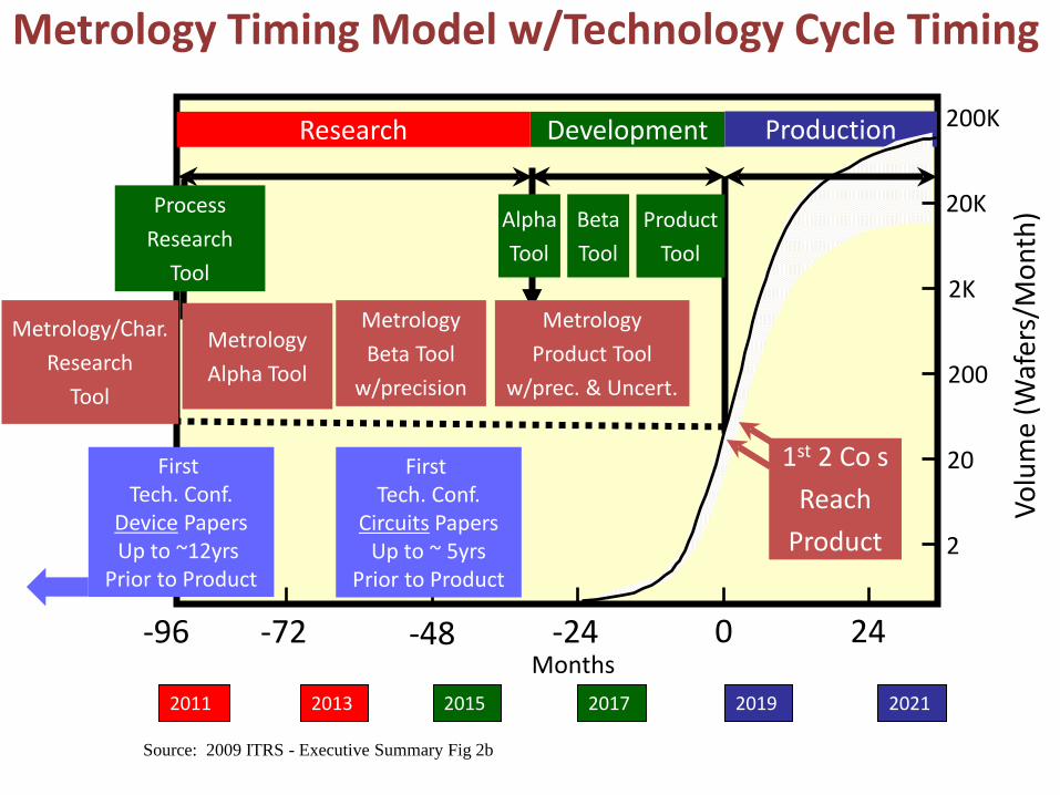
Metrology Timing Model w/Technology Cycle Timing
Source: 2009 ITRS - Executive Summary Fig 2b
Months
Development Production
Volu
me
(Waf
ers/
Mon
th)
2
20
200
2K
20K
200K Research
-72 0 24 -48 -24 -96
First Tech. Conf.
Device Papers Up to ~12yrs
Prior to Product
2019 2017 2015 2013 2011 2021
1st 2 Co s Reach
Product
First Tech. Conf.
Circuits Papers Up to ~ 5yrs
Prior to Product
Process Research
Tool
Alpha Tool
Beta Tool
Product Tool
Metrology/Char. Research
Tool
Metrology Alpha Tool
Metrology Product Tool
w/prec. & Uncert.
Metrology Beta Tool
w/precision

AGENDA
• Metrology for Extreme CMOS – 15 Year Horizon? – FEP Metrology – Lithography Metrology – Interconnect Metrology
• Metrology for Beyond CMOS – Graphene Devices – Other Devices
• Key Message about the Future
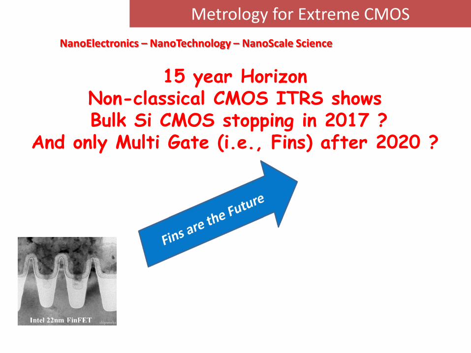
Extreme CMOS
15 year Horizon Non-classical CMOS ITRS shows Bulk Si CMOS stopping in 2017 ?
And only Multi Gate (i.e., Fins) after 2020 ?
NanoElectronics – NanoTechnology – NanoScale Science
Metrology for Extreme CMOS
Intel 22nm FinFET

AGENDA
• Metrology for Extreme CMOS – 15 Year Horizon? – FEP Metrology – Lithography Metrology – Interconnect Metrology
• Metrology for Beyond CMOS – Graphene Devices – Other Devices
• Key Message about the Future
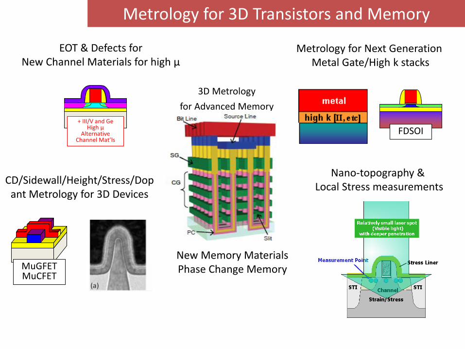
Metrology for Next Generation Metal Gate/High k stacks
EOT & Defects for New Channel Materials for high µ
Nano-topography & Local Stress measurements
New Memory Materials Phase Change Memory
FDSOI
MuGFET MuCFET
+ III/V and Ge High µ
Alternative Channel Mat’ls
CD/Sidewall/Height/Stress/Dopant Metrology for 3D Devices
Metrology for 3D Transistors and Memory
3D Metrology for Advanced Memory
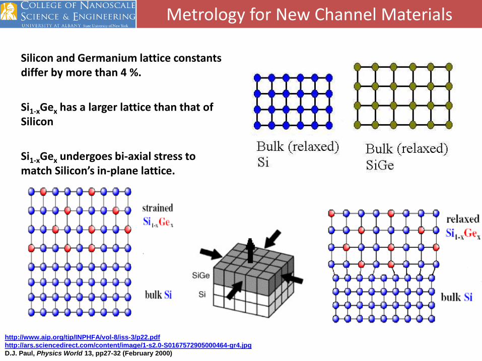
Silicon and Germanium lattice constants differ by more than 4 %. Si1-xGex has a larger lattice than that of Silicon Si1-xGex undergoes bi-axial stress to match Silicon’s in-plane lattice.
cnse.albany.edu
9
http://www.aip.org/tip/INPHFA/vol-8/iss-3/p22.pdf http://ars.sciencedirect.com/content/image/1-s2.0-S0167572905000464-gr4.jpg D.J. Paul, Physics World 13, pp27-32 (February 2000)
Metrology for New Channel Materials
Rock w/ Coupled ω-2θ
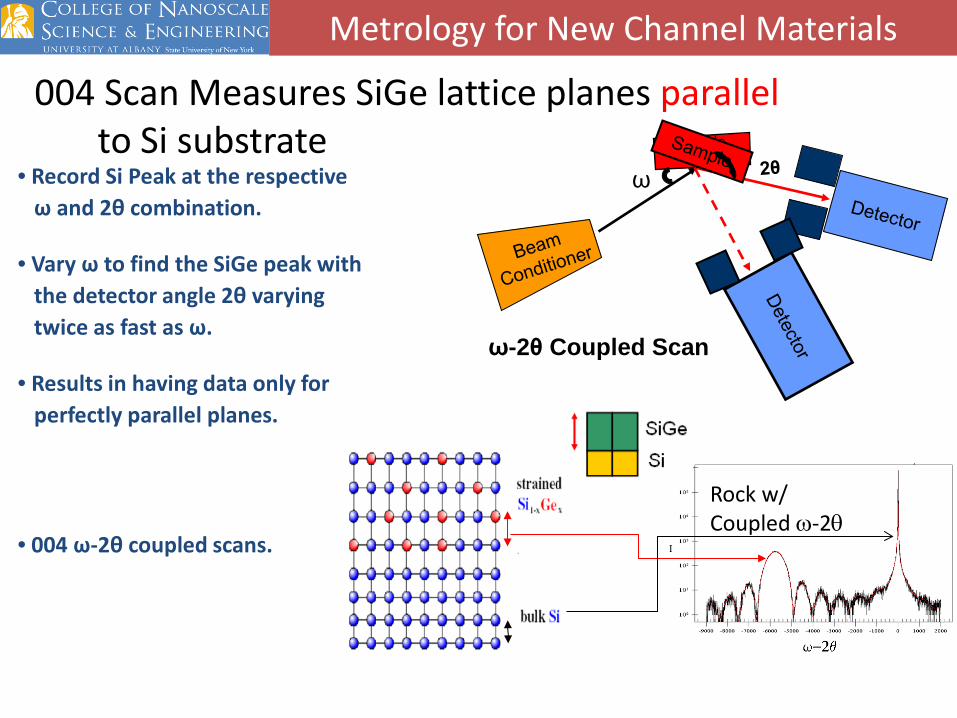
• Record Si Peak at the respective ω and 2θ combination.
• Vary ω to find the SiGe peak with the detector angle 2θ varying twice as fast as ω.
• Results in having data only for perfectly parallel planes.
• 004 ω-2θ coupled scans.
cnse.albany.edu
10
ω
ω-2θ Coupled Scan
High Resolution ω-2θ Coupled Scans 004 Scan Measures SiGe lattice planes parallel to Si substrate
Metrology for New Channel Materials
cnse.albany.edu
11
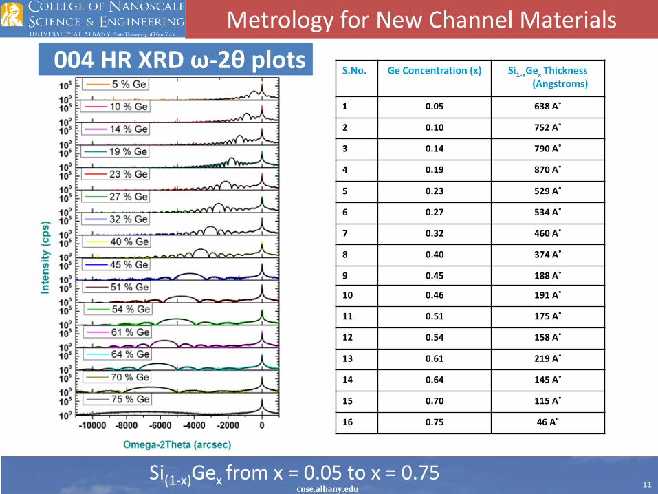
S.No. Ge Concentration (x) Si1-xGex Thickness (Angstroms)
1 0.05 638 A˚
2 0.10 752 A˚
3 0.14 790 A˚
4 0.19 870 A˚
5 0.23 529 A˚
6 0.27 534 A˚
7 0.32 460 A˚
8 0.40 374 A˚
9 0.45 188 A˚
10 0.46 191 A˚
11 0.51 175 A˚
12 0.54 158 A˚
13 0.61 219 A˚
14 0.64 145 A˚
15 0.70 115 A˚
16 0.75 46 A˚
004 HR XRD ω-2θ plots
Si(1-x)Gex from x = 0.05 to x = 0.75
Metrology for New Channel Materials
-2000 -1000 0 1000 2000-4000
-2000
0
2000
Omega_Rel (arcsec)
Omeg
a-2T
heta
(arc
sec)
1.0001.2001.4001.6001.8002.0002.2002.4002.6002.8003.000
We record ω - 2θ coupled scan intensities for varying ω angles. – Start with ω - 2θ coupled scans.
– Fixing 2θ, slightly vary ω ω-rel.
– We get a Si Peak at a Particular ω - 2θ – [ω-rel]a and a SiGe peak at another ω - 2θ – [ω-rel]b.
If there is no tilt -- SiGe peak at the same ω-rel angle as Silicon’s.
A tilted layer gives the SiGe peak at a different ω - 2θ for that particular d-spacing and at a different ω - rel angle.
12
2θ ω
004 Reciprocal Space Maps
Metrology for New Channel Materials
-50 -25 0 25 50-200
-150
-100
-50
0
50
Q (110) 1/um
Q (
001)
1/u
m
1.0001.2001.4001.6001.8002.0002.2002.4002.6002.8003.000
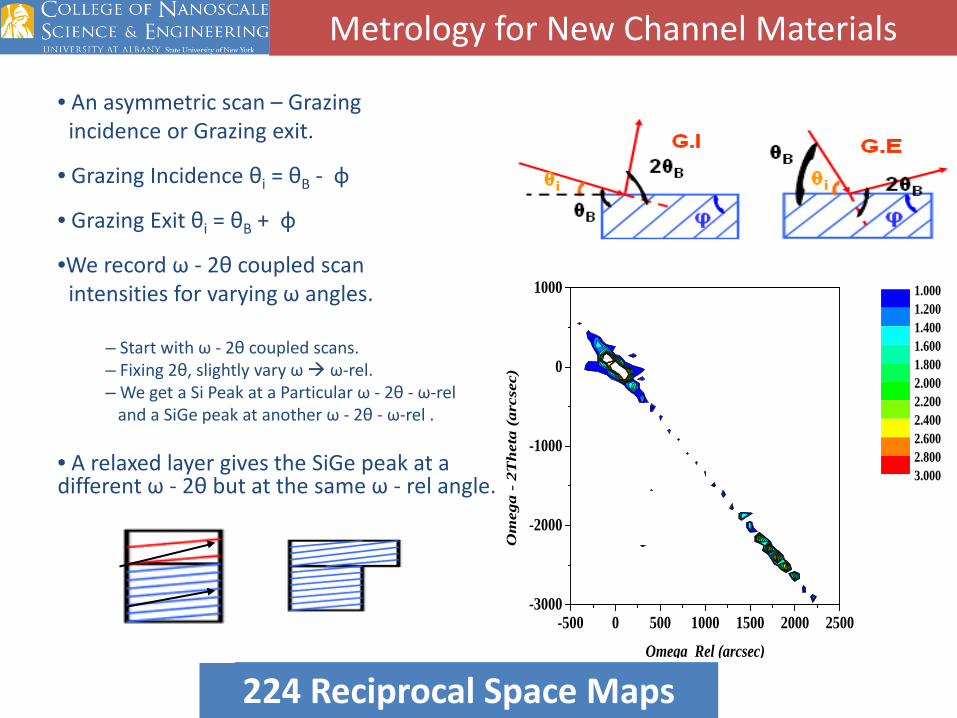
• An asymmetric scan – Grazing incidence or Grazing exit.
• Grazing Incidence θi = θB - φ
• Grazing Exit θi = θB + φ
•We record ω - 2θ coupled scan intensities for varying ω angles.
– Start with ω - 2θ coupled scans. – Fixing 2θ, slightly vary ω ω-rel. – We get a Si Peak at a Particular ω - 2θ - ω-rel and a SiGe peak at another ω - 2θ - ω-rel .
• A relaxed layer gives the SiGe peak at a different ω - 2θ but at the same ω - rel angle.
13 224 Reciprocal Space Maps
-500 0 500 1000 1500 2000 2500-3000
-2000
-1000
0
1000
Omega Rel (arcsec)
Om
ega
- 2T
het
a (a
rcse
c)
1.0001.2001.4001.6001.8002.0002.2002.4002.6002.8003.000
Metrology for New Channel Materials
14
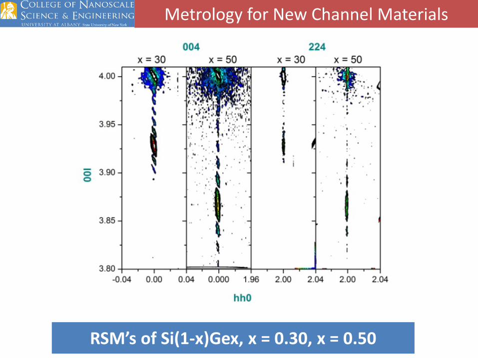
RSM’s of Si(1-x)Gex, x = 0.30, x = 0.50
Metrology for New Channel Materials
15
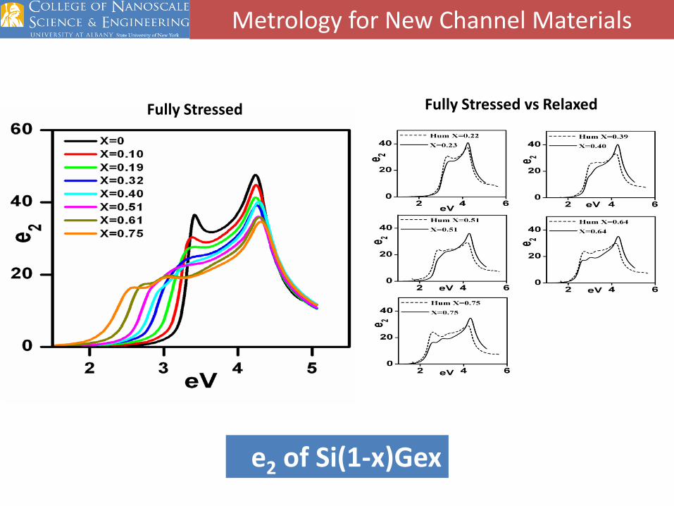
e2 of Si(1-x)Gex
Fully Stressed Fully Stressed vs Relaxed
Metrology for New Channel Materials
16
Metrology for New Channel Materials
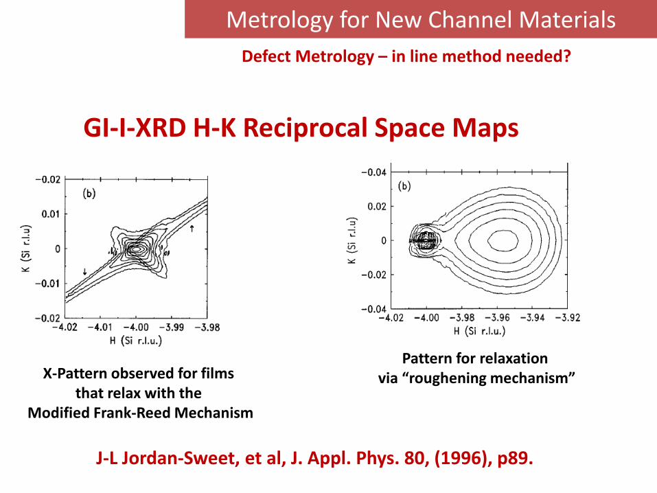
GI-I-XRD H-K Reciprocal Space Maps
Defect Metrology – in line method needed?
X-Pattern observed for films that relax with the
Modified Frank-Reed Mechanism
Pattern for relaxation via “roughening mechanism”
J-L Jordan-Sweet, et al, J. Appl. Phys. 80, (1996), p89.
Tong
, et a
l, IE
EE T
rans
actio
ns o
n N
ucle
ar S
cien
ce, 5
7,(2
010)
, p
1640
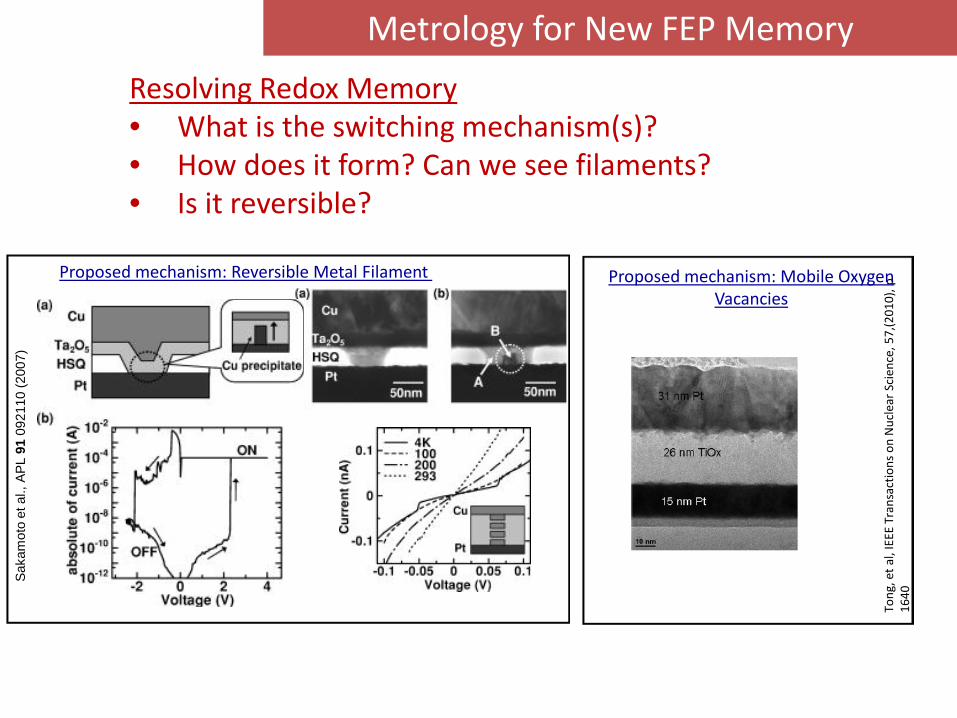
Metrology for New FEP Memory Resolving Redox Memory • What is the switching mechanism(s)? • How does it form? Can we see filaments? • Is it reversible?
Saka
mot
o et
al.,
APL
91
0921
10 (2
007)
Proposed mechanism: Reversible Metal Filament Proposed mechanism: Mobile Oxygen Vacancies
New Materials impact CD Metrology
wavelength
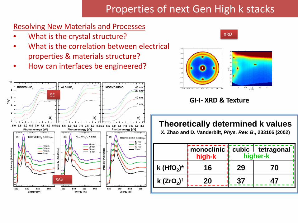
Properties of next Gen High k stacks Resolving New Materials and Processes • What is the crystal structure? • What is the correlation between electrical
properties & materials structure? • How can interfaces be engineered?
SE
XAS
XRD
X. Zhao and D. Vanderbilt, Phys. Rev. B., 233106 (2002) Theoretically determined k values
monoclinic cubic tetragonal
k (HfO2)* 16 29 70 k (ZrO2)† 20 37 47
high-k higher-k
GI-I- XRD & Texture
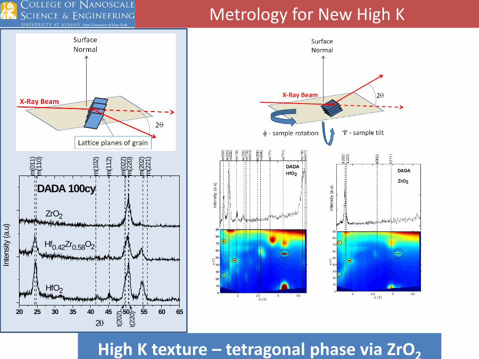
19 High K texture – tetragonal phase via ZrO2
20 25 30 35 40 45 50 55 60 65
DADA 100cy
m(1
12)
Hf0.42Zr0.58O2
ZrO2
m(2
02)
Inte
nsity
(a.u
)
2θ t(220
)
t(202
)
m(1
02)
m(1
10)
m(0
11)
m(0
22)
m(2
20)
m(2
21)
HfO2
Metrology for New High K
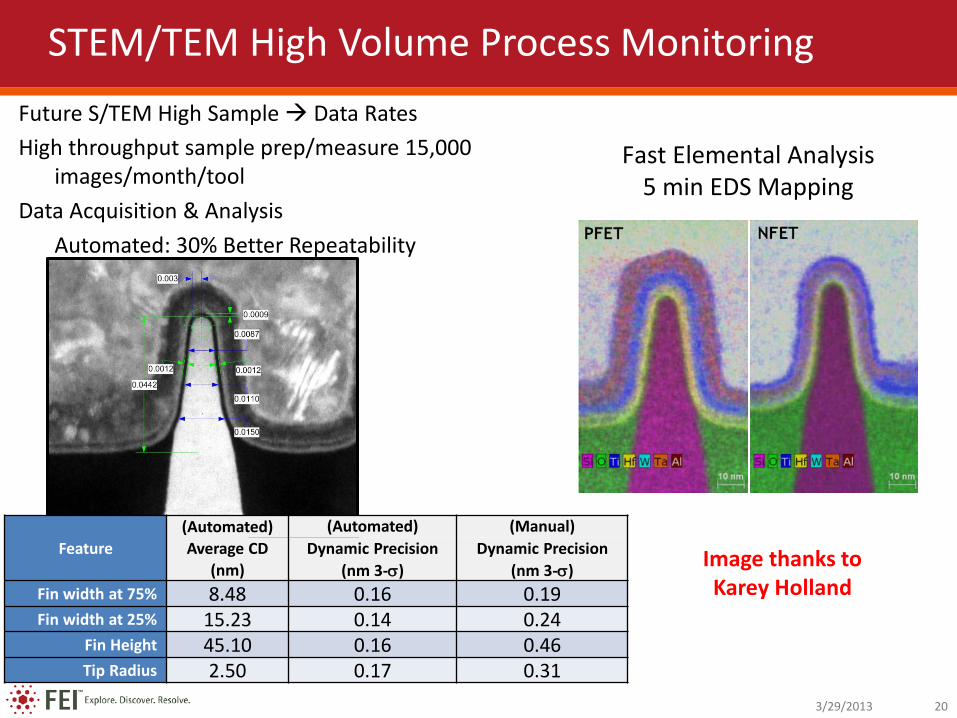
STEM/TEM High Volume Process Monitoring
3/29/2013 20
Future S/TEM High Sample Data Rates High throughput sample prep/measure 15,000
images/month/tool Data Acquisition & Analysis Automated: 30% Better Repeatability
Feature (Automated) (Automated) (Manual) Average CD Dynamic Precision Dynamic Precision
(nm) (nm 3-σ) (nm 3-σ) Fin width at 75% 8.48 0.16 0.19 Fin width at 25% 15.23 0.14 0.24
Fin Height 45.10 0.16 0.46 Tip Radius 2.50 0.17 0.31
Fast Elemental Analysis 5 min EDS Mapping
Image thanks to Karey Holland
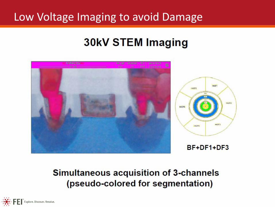
Low Voltage Imaging to avoid Damage

AGENDA
• Metrology for Extreme CMOS – 15 Year Horizon? – FEP Metrology – Lithography Metrology – Interconnect Metrology
• Metrology for Beyond CMOS – Graphene Devices – Other Devices
• Key Message about the Future
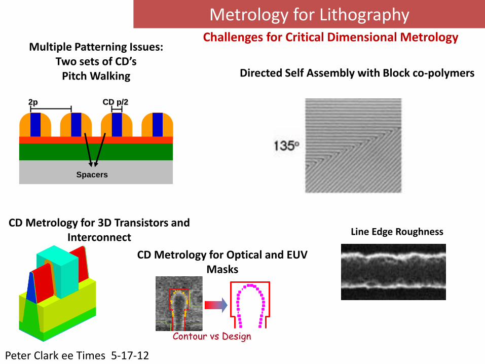
Multiple Patterning Issues: Two sets of CD’s
Pitch Walking
Line Edge Roughness CD Metrology for 3D Transistors and
Interconnect
Contour vs Design
Metrology for Lithography Challenges for Critical Dimensional Metrology
2p
Spacers
CD p/2
Directed Self Assembly with Block co-polymers
Peter Clark ee Times 5-17-12
CD Metrology for Optical and EUV Masks
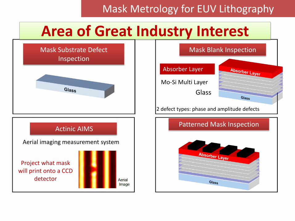
Mask Blank Inspection Mask Substrate Defect Inspection
Actinic AIMS Patterned Mask Inspection
Mo-Si Multi Layer
Absorber Layer
Glass
Project what mask will print onto a CCD
detector
Mask Metrology for EUV Lithography
Aerial imaging measurement system
2 defect types: phase and amplitude defects
Area of Great Industry Interest
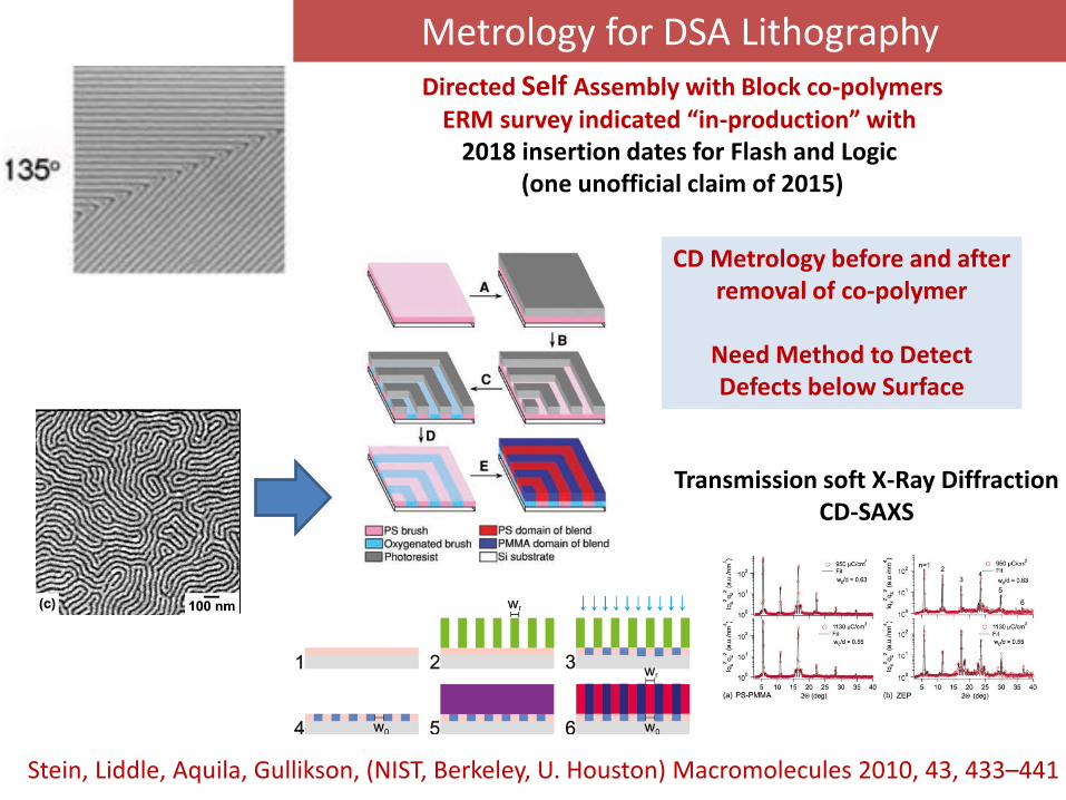
Metrology for DSA Lithography Directed Self Assembly with Block co-polymers
ERM survey indicated “in-production” with 2018 insertion dates for Flash and Logic
(one unofficial claim of 2015)
Stein, Liddle, Aquila, Gullikson, (NIST, Berkeley, U. Houston) Macromolecules 2010, 43, 433–441
Transmission soft X-Ray Diffraction CD-SAXS
CD Metrology before and after removal of co-polymer
Need Method to Detect Defects below Surface
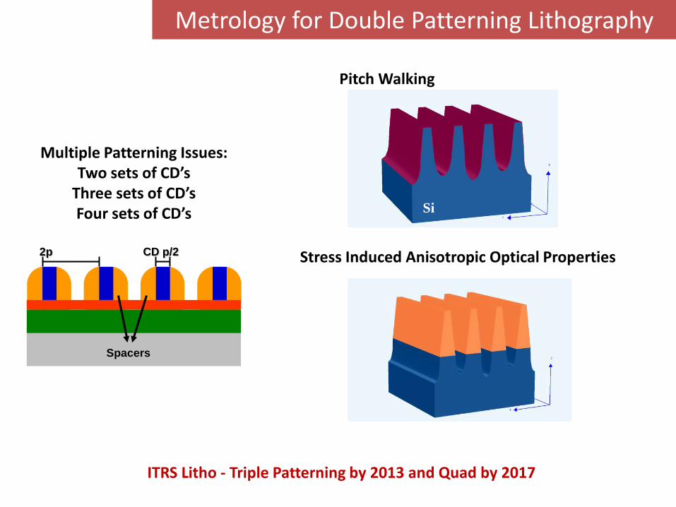
Metrology for Double Patterning Lithography
Multiple Patterning Issues: Two sets of CD’s
Three sets of CD’s Four sets of CD’s
2p
Spacers
CD p/2
Si
Pitch Walking
Stress Induced Anisotropic Optical Properties
ITRS Litho - Triple Patterning by 2013 and Quad by 2017
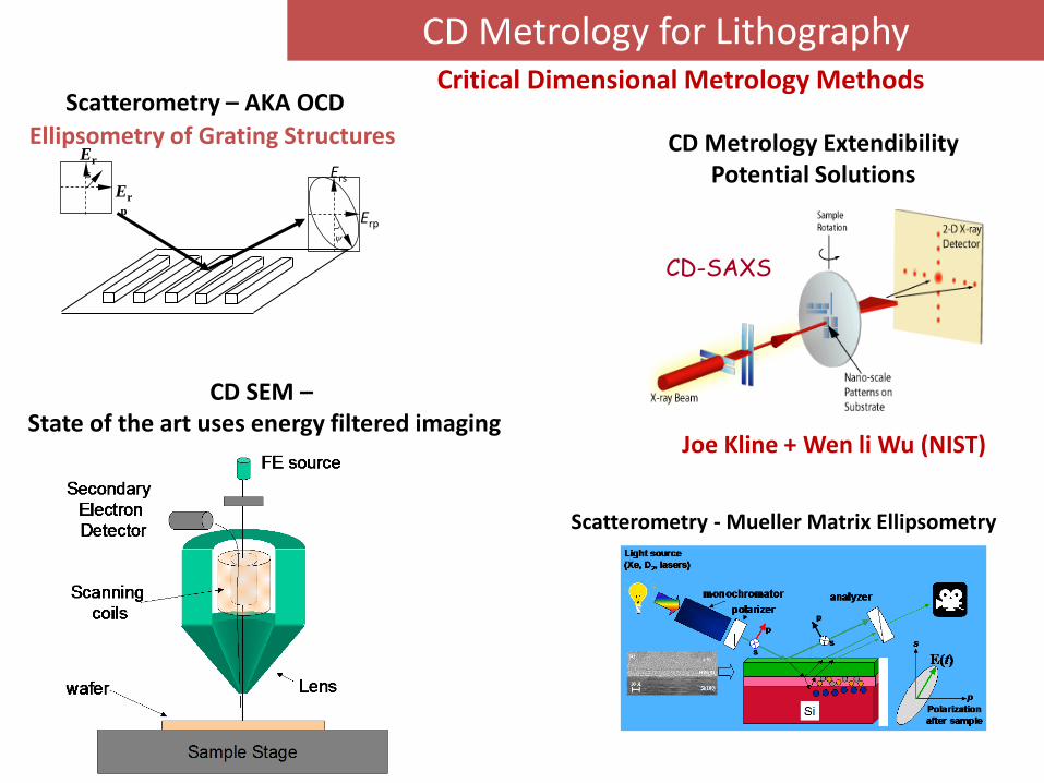
CD Metrology Extendibility Potential Solutions
CD-SAXS
Scatterometry - Mueller Matrix Ellipsometry
CD Metrology for Lithography Critical Dimensional Metrology Methods
CD SEM – State of the art uses energy filtered imaging
Scatterometry – AKA OCD
ψ
Ers
Erp
Ellipsometry of Grating Structures Er
s Erp
Joe Kline + Wen li Wu (NIST)
29 March 2013 28
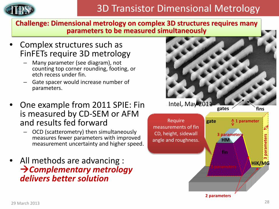
• Complex structures such as FinFETs require 3D metrology
– Many parameter (see diagram), not counting top corner rounding, footing, or etch recess under fin.
– Gate spacer would increase number of parameters.
• One example from 2011 SPIE: Fin is measured by CD-SEM or AFM and results fed forward
– OCD (scatterometry) then simultaneously measures fewer parameters with improved measurement uncertainty and higher speed.
• All methods are advancing : Complementary metrology delivers better solution
2 parameters
gate
fin
HM
HiK/MG 3 parameters
3 parameters
3 pa
ram
eter
s
1 parameter
fins gates
Require measurements of fin CD, height, sidewall
angle and roughness.
3D Transistor Dimensional Metrology
Intel, May 2011
Challenge: Dimensional metrology on complex 3D structures requires many parameters to be measured simultaneously
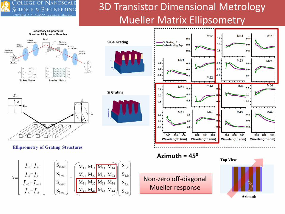
3D Transistor Dimensional Metrology Mueller Matrix Ellipsometry
Azimuth
Top View Azimuth = 450
Non-zero off-diagonal Mueller response
SiGe Grating
Si Grating
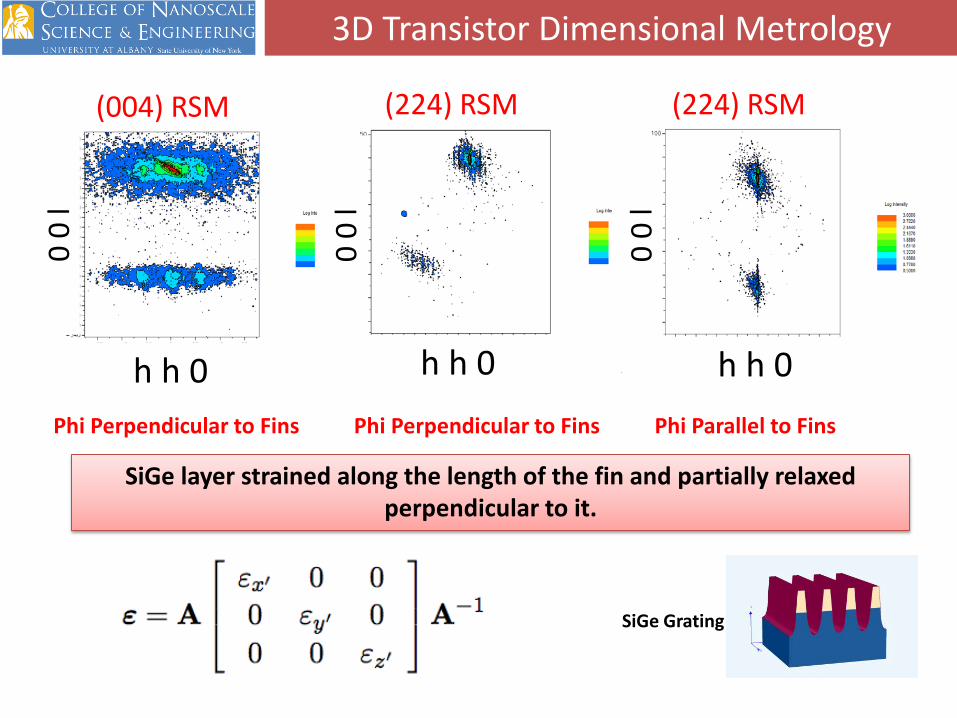
SiGe Grating –RSM HRXRD
SiGe layer strained along the length of the fin and partially relaxed perpendicular to it.
SiGe Grating
3D Transistor Dimensional Metrology
Phi Perpendicular to Fins Phi Perpendicular to Fins Phi Parallel to Fins
(004) RSM (224) RSM (224) RSM
h h 0 h h 0 h h 0
0 0
l
0 0
l
0 0
l
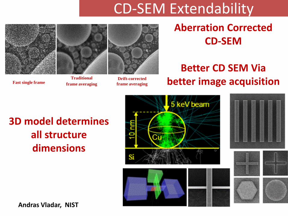
CD-SEM Extendability
Drift-corrected frame averaging
Traditional frame averaging Fast single frame
3D model determines all structure dimensions
Andras Vladar, NIST
Aberration Corrected CD-SEM
Better CD SEM Via
better image acquisition
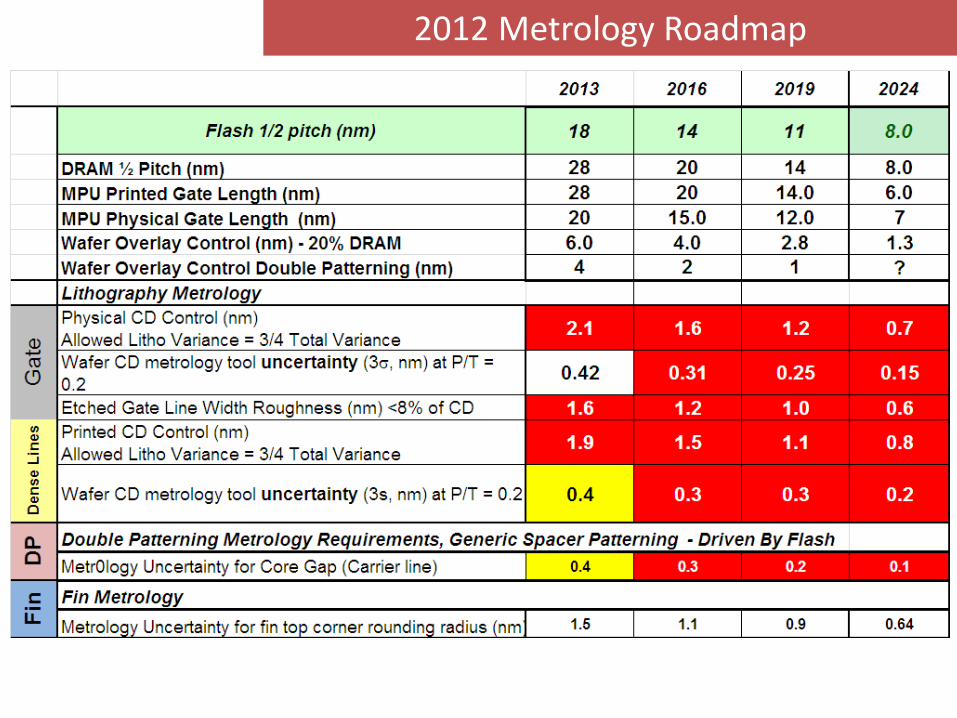
2012 Metrology Roadmap

AGENDA
• Metrology for Extreme CMOS – 15 Year Horizon? – FEP Metrology – Lithography Metrology – Interconnect Metrology
• Metrology for Beyond CMOS – Graphene Devices – Other Devices
• Key Message about the Future
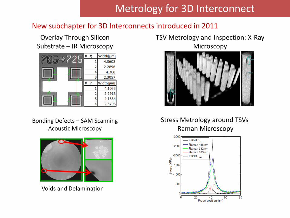
TSV Metrology and Inspection: X-Ray Microscopy
Overlay Through Silicon Substrate – IR Microscopy
Bonding Defects – SAM Scanning Acoustic Microscopy
Metrology for 3D Interconnect New subchapter for 3D Interconnects introduced in 2011
Voids and Delamination
Stress Metrology around TSVs Raman Microscopy

AGENDA
• Metrology for Extreme CMOS – 15 Year Horizon? – Lithography Metrology – FEP Metrology – Interconnect Metrology
• Metrology for Beyond CMOS – Graphene Devices – Other Devices
• Key Message about the Future
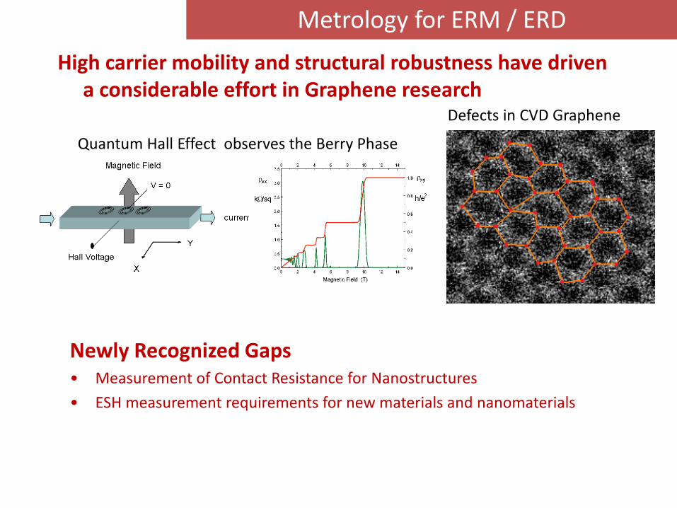
High carrier mobility and structural robustness have driven a considerable effort in Graphene research
Defects in CVD Graphene
Quantum Hall Effect observes the Berry Phase
Metrology for ERM / ERD
Newly Recognized Gaps • Measurement of Contact Resistance for Nanostructures • ESH measurement requirements for new materials and nanomaterials
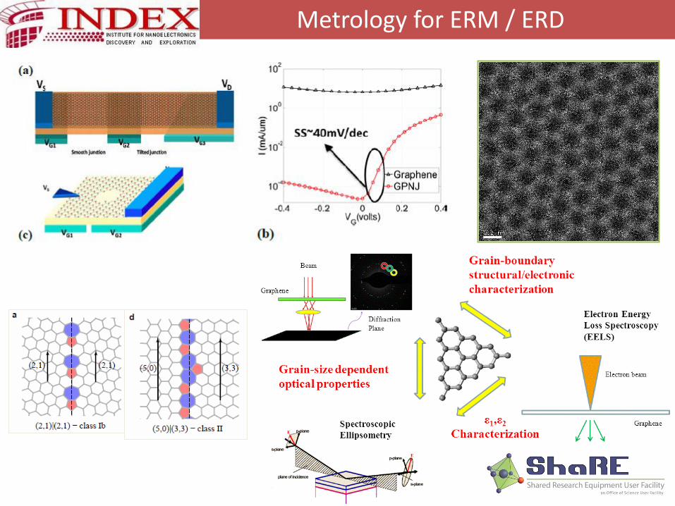
Metrology for ERM / ERD
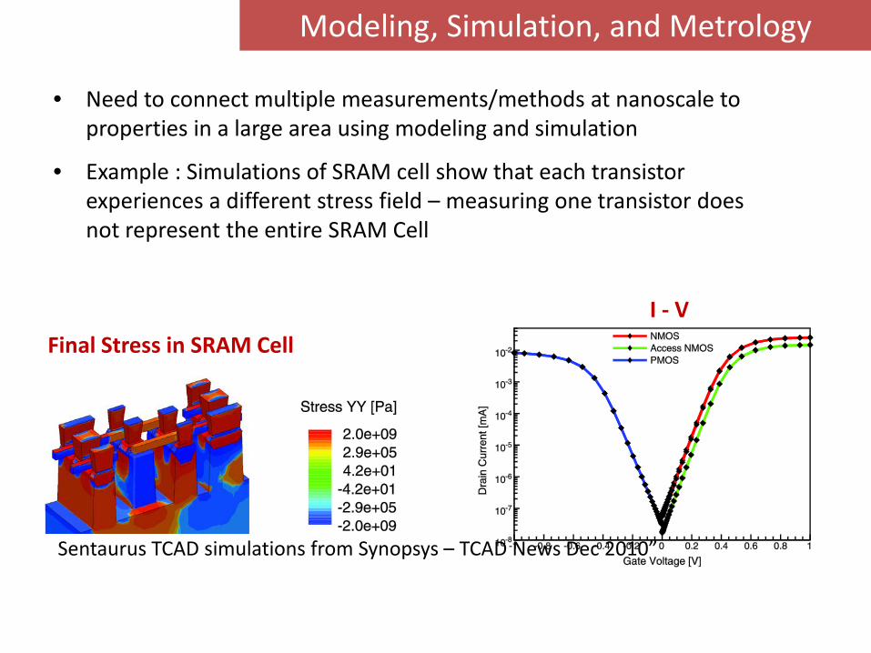
Modeling, Simulation, and Metrology
Final Stress in SRAM Cell I - V
“Sentaurus TCAD simulations from Synopsys – TCAD News Dec 2010”
• Need to connect multiple measurements/methods at nanoscale to properties in a large area using modeling and simulation
• Example : Simulations of SRAM cell show that each transistor experiences a different stress field – measuring one transistor does not represent the entire SRAM Cell
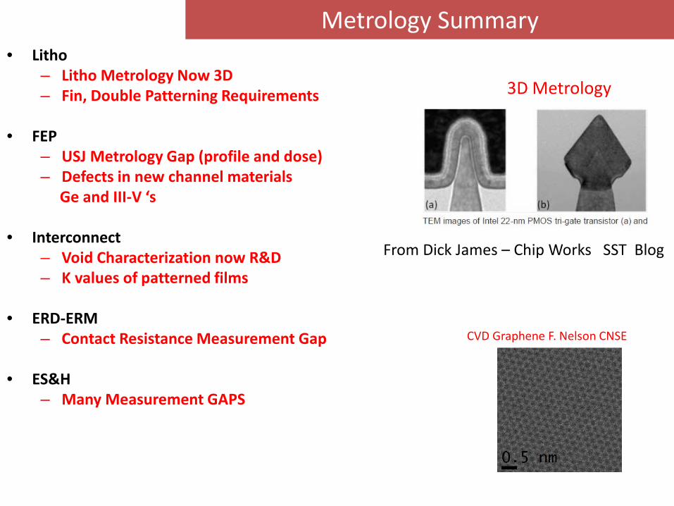
• Litho – Litho Metrology Now 3D – Fin, Double Patterning Requirements
• FEP
– USJ Metrology Gap (profile and dose) – Defects in new channel materials Ge and III-V ‘s
• Interconnect
– Void Characterization now R&D – K values of patterned films
• ERD-ERM
– Contact Resistance Measurement Gap
• ES&H – Many Measurement GAPS
3D Metrology
CVD Graphene F. Nelson CNSE
From Dick James – Chip Works SST Blog
Metrology Summary
• Effects of stress on the dielectric function of strained pseudomorphic Si1-xGex alloys from 0 to 75 % Ge grown on Si (001) G.R. Muthinti, M. Medikonda, T.N. Adam, A. Reznicek, and A.C. Diebold, J. Appl. Phys. 112, (2012), 053519.
• Fin Pitch and Stress Measurement using X-Ray Diffraction Reciprocal Space Maps and Optical Scatterometry, A.C. Diebold, M. Medikonda, G.R. Muthinti, V. Kamenini, J. Fronheiser, M. Wormington, B. Peterson, and J. Race, Metrology, Inspection, and Process Control for Microlithography XXVII, SPIE Advanced Lithography, San Jose, Feb 24-March 1, 2013.
• Mueller based scatterometry measurement of nanoscale structures with anisotropic in-plane
optical properties, G.R.Muthinti, M. Medikonda, J. Fronheiser, V.Kamineni, B. Peterson, J. Race, W.McGahan, S. Rabello, and A. C. Diebold, Metrology, Inspection, and Process Control for Microlithography XXVII, SPIE Advanced Lithography, San Jose, Feb 24-March 1, 2013.
• Mueller based scatterometry measurement of nanoscale structures with anisotropic in-plane optical properties, G.R.Muthinti, M. Medikonda, J. Fronheiser, V.Kamineni, B. Peterson, J. Race, W.McGahan, S. Rabello, and A. C. Diebold, Metrology, Inspection, and Process Control for Microlithography XXVII, San Jose, Feb 13-16, 2012.
• Investigation of E-beam patterned nanostructures using Mueller Matrix based Scatterometry, G.R. Muthinti, B. Peterson, and A.C. Diebold, Metrology, Inspection, and Process Control for Microlithography XXVI, SPIE Advanced Lithography, San Jose, Feb 13-16, 2012.
• A.C. Diebold and R. Matyi, SRC White Paper, 2007
cnse.albany.edu
40
References