Pre-Baseline Pixel R&D Simon Kwan BTeV Electronics & Software Mtg., May 24,2001 And BTeV Coll. Mtg.,...
31
Pre-Baseline Pixel R&D Simon Kwan BTeV Electronics & Software Mtg., May 24,2001 And BTeV Coll. Mtg., May 25, 2001
-
Upload
eleanore-heath -
Category
Documents
-
view
218 -
download
0
Transcript of Pre-Baseline Pixel R&D Simon Kwan BTeV Electronics & Software Mtg., May 24,2001 And BTeV Coll. Mtg.,...
Pre-Baseline Pixel R&D
Simon Kwan
BTeV Electronics & Software Mtg., May 24,2001
And BTeV Coll. Mtg., May 25, 2001

WBS Level 3 Activities
• Sensor and Pixel Detector Hybridization
• Readout Electronics
• Mechanical support, cooling and vacuum systems
• System integration
• Project Management

Sensor and Hybridization
• Sensor– FNAL and Syracuse– Good progress on measurements at FNAL
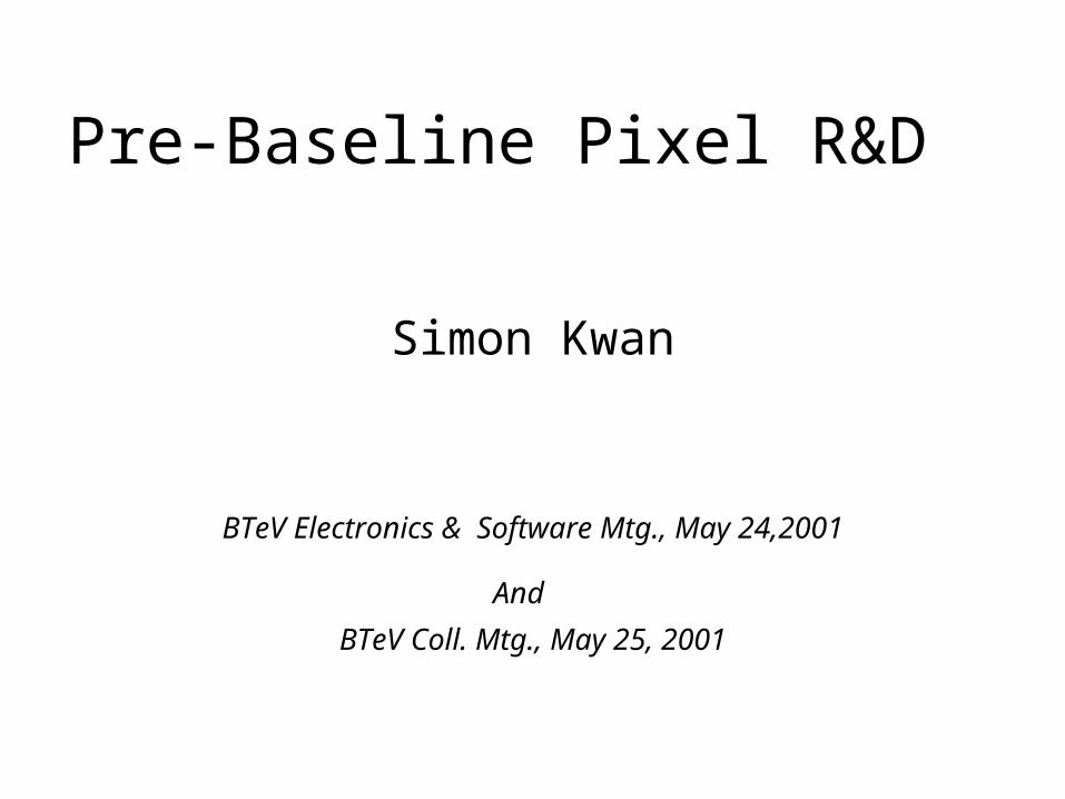
• I-V, C-V, voltage distribution on guard-rings measured on wafers and single dies of various structures (diodes and pixels) using different p-stop designs and 3 different guard-ring designs from different sources
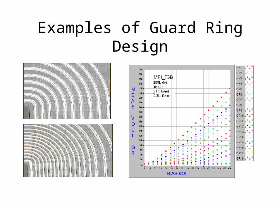
• Normal and oxygenated wafers• Will also measure interpixel capacitance and interpixel resistance • Effect of temperature(cold-chuck), humidity, dicing, cleaning• Will extend to different resistivity, p-spray technologies from different
vendors• Irradiation studies• Laser test stand setup to study effect of magnetic field (before and after
irradiation)• Will have most of the results we want for the baseline review
Examples of Guard Ring Design
SINTEF Sensor WaferBreakdown Voltage

Sensor (cont’d)
• Syracuse University– 3D Simulation program
– Probe station and accessories
– Lack of NSF money hampers the effort
– Need support to get a laser test stand
– Start assembly of FPIX0 detectors (extended finger to bias the p-stop)
Detector Hybridization• Rec’d 11 detectors and 2 modules made using both
Indium(4+1) and Pb/Sn bumps (7+1)• Long term test, thermal cycle + irradiation tests on
dummies now under way• Remaining issue : 8” wafer and thinning• Existing contract with MCNC to do assembly from 8”
dummies provided by CERN. AIT claimed that they have 8” capability
• Thinning – program of studies; working together with MCNC (issues: flatness, stress, probing, dicing after thinning, bump protection)
• Yield and quality assurance – work in progress with vendor
Readout Electronics• preFPIX2 Pixel Readout Chip
– preFPIX2Tb – SEU tests last month; more test early June, also total dosage effects
– Detectors using preFPIX2Tb – expected delivery in the summer; irradiation tests planned for September
– preFPIX2Ti : may get 1 or more detectors from UCD; still negotiating with CERN to get 1 complete wafer
• Development path to FPIX2 and production chip– Needs a consensus (dynamic range, threshold dispersion, number of
serial lines, serialization scheme,pads, iterations)– Features (e.g. Pattern to check bump bonding)– Specification document (summer)– Schedule
• Complete engineering run Dec 01?• Small chip with complete readout via MOSIS (MPW)• Split submission with SVX4: submission in Oct 01 with another
submission in 2002

High Density Flex Cable• Expected delivery of flex-
circuits from CERN next week
• PCB being procured to test the circuit and bare FPIX1 chips before moving to detector module
• Plan to address assembly issue
• Embark on a comprehensive program of studies on adhesives
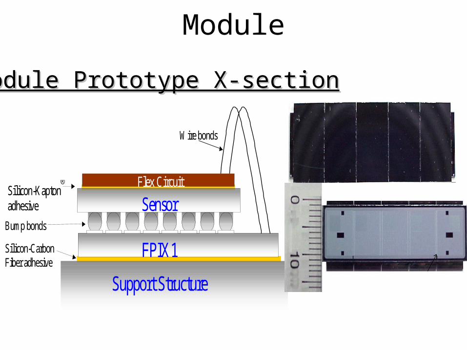
FPIX1
Sensor
Flex Circuit
Support Structure
Silicon-Kapton
adhesive
Silicon-Carbon Fiber adhesive
Bump bonds
Wire bonds
Module Prototype X-sectionModule Prototype X-section
Module
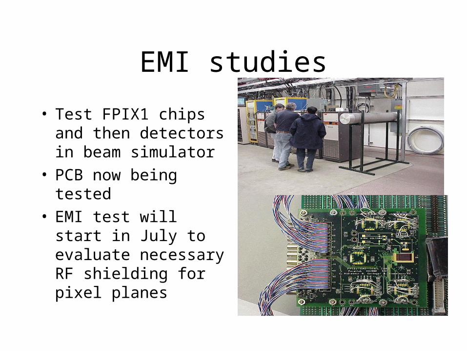
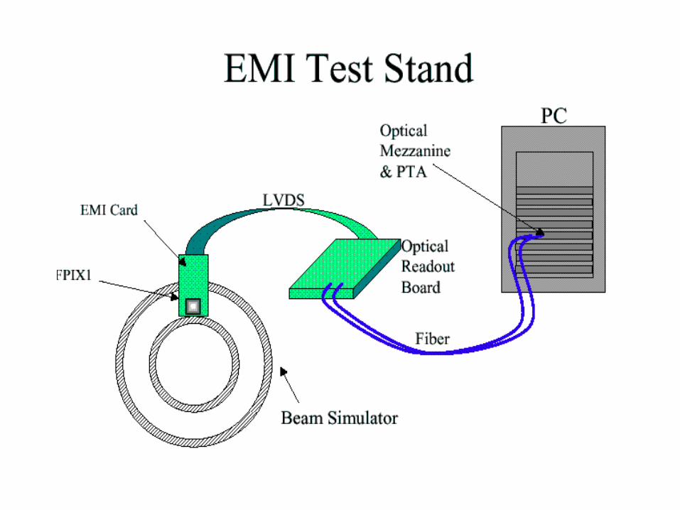
EMI studies
• Test FPIX1 chips and then detectors in beam simulator
• PCB now being tested• EMI test will start in
July to evaluate necessary RF shielding for pixel planes
Data Combiner board
• Study number of serial lines, maximum clock frequency as function of chip size and number of interactions per BCO
• Working on input protocol from the pixel module to the board
• Plan to have a pixel module simulator and Data Combiner Board simulator tested in the summer
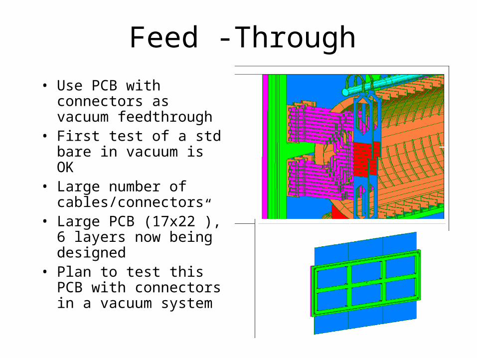
Feed -Through
• Use PCB with connectors as vacuum feedthrough
• First test of a std bare in vacuum is OK
• Large number of cables/connectors
• Large PCB (17x22”), 6 layers now being designed
• Plan to test this PCB with connectors in a vacuum system
Misc.
• PCI test stand ( working)• Test beam preparation (needs help from university
groups and maybe software professional)• HV and LV power supply, connectors (HV
workshop; compact, high density HV connector, simple RGS125 cable; Document being prepared summarizing all the requirements and the choices provided by the vendors)
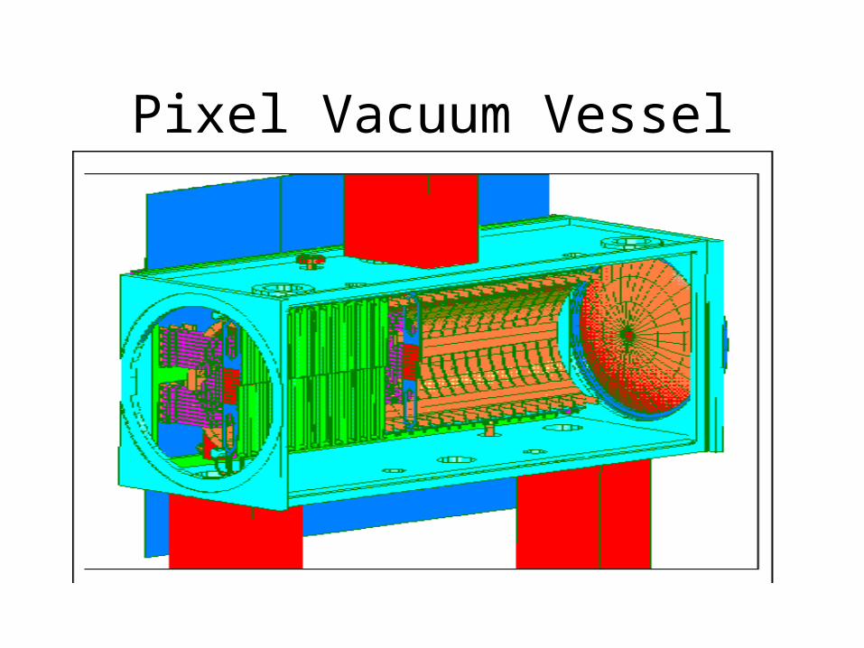
Pixel Vacuum Vessel
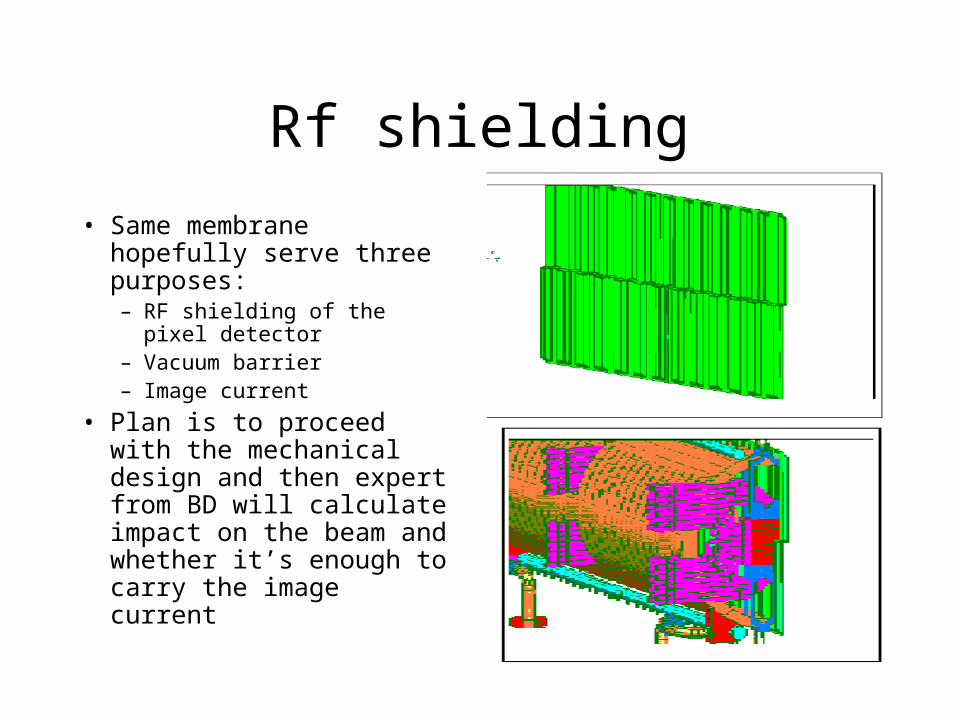
Rf shielding
• Same membrane hopefully serve three purposes:– RF shielding of the pixel
detector– Vacuum barrier– Image current
• Plan is to proceed with the mechanical design and then expert from BD will calculate impact on the beam and whether it’s enough to carry the image current
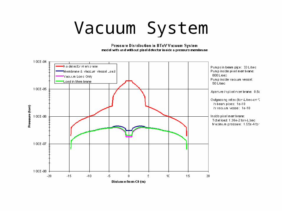
Vacuum System
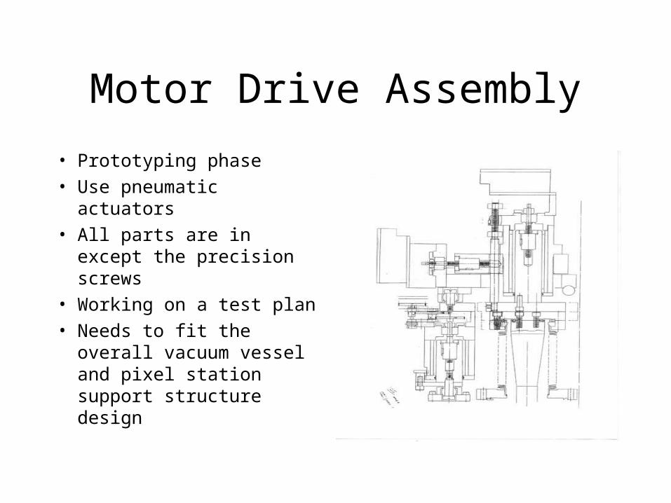
Motor Drive Assembly
• Prototyping phase
• Use pneumatic actuators
• All parts are in except the precision screws
• Working on a test plan
• Needs to fit the overall vacuum vessel and pixel station support structure design
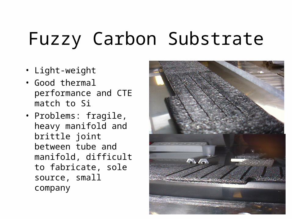
Fuzzy Carbon Substrate
• Light-weight
• Good thermal performance and CTE match to Si
• Problems: fragile, heavy manifold and brittle joint between tube and manifold, difficult to fabricate, sole source, small company

Cooling Test Results on fuzzy carbon substrate
• Used water/glycol mix (70/30 by wt)
• Neslab chiller to set temp• Small pump to get the flow rate• Flow-meter calibration to the
mixture• Hydrometer to check density of
mix• Filter, insulator, glove box(dry N2)• SMT resistors as heaters• RTDs to readout temperature (5
points; water inlet and outlet line, fuzzy carbon surface-entry,notch, exit)
• Also monitor pressure drop, absolute pressure of inlet
• Haven’t used laser to monitor vibration
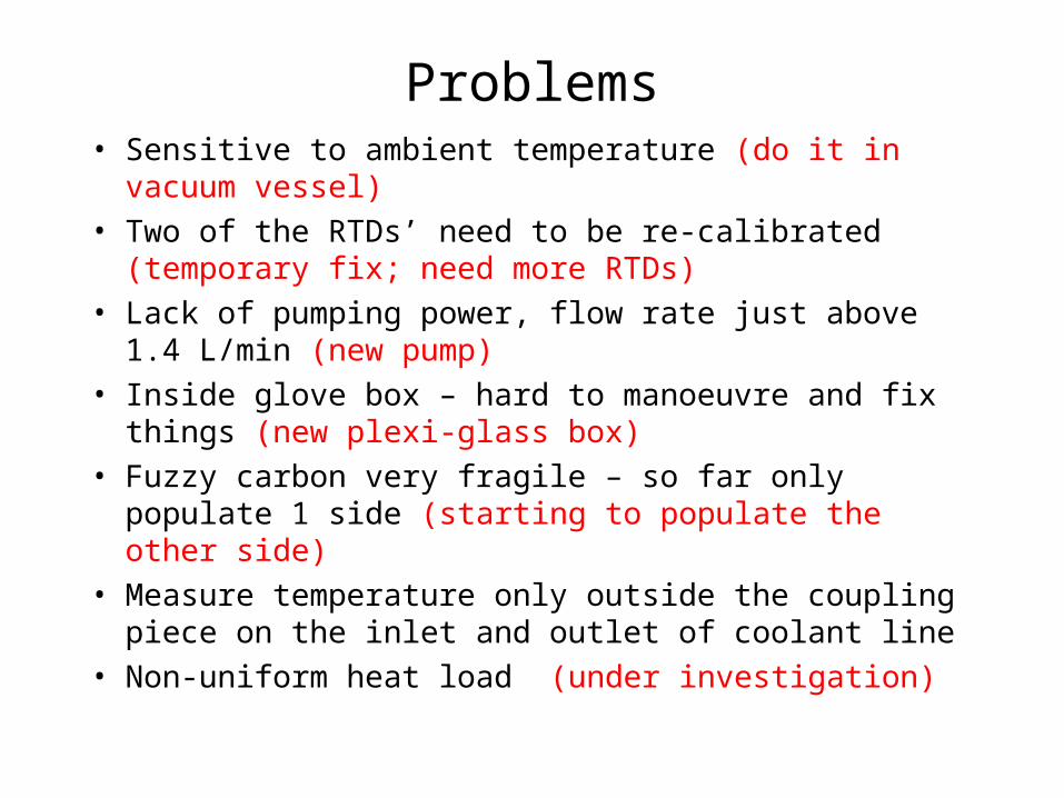
Problems• Sensitive to ambient temperature (do it in vacuum vessel)
• Two of the RTDs’ need to be re-calibrated (temporary fix; need more RTDs)
• Lack of pumping power, flow rate just above 1.4 L/min (new pump)
• Inside glove box – hard to manoeuvre and fix things (new plexi-glass box)
• Fuzzy carbon very fragile – so far only populate 1 side (starting to populate the other side)
• Measure temperature only outside the coupling piece on the inlet and outlet of coolant line
• Non-uniform heat load (under investigation)
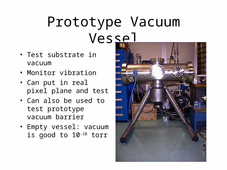
Prototype Vacuum Vessel
• Test substrate in vacuum
• Monitor vibration
• Can put in real pixel plane and test
• Can also be used to test prototype vacuum barrier
• Empty vessel: vacuum is good to 10-10 torr
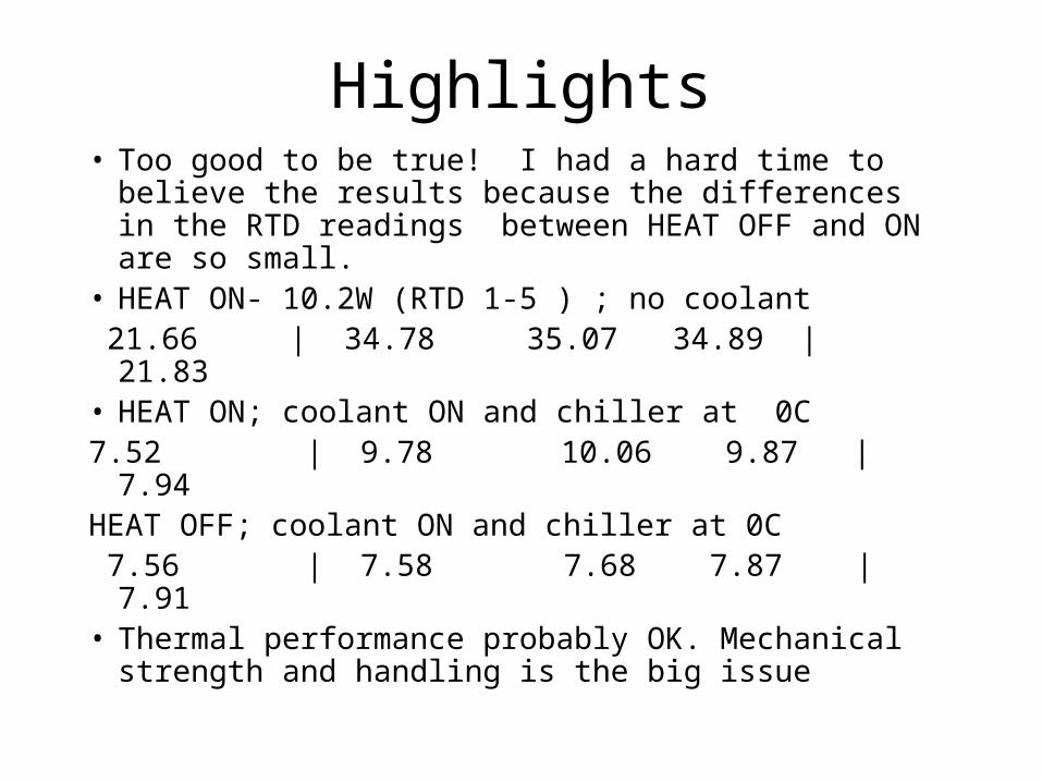
Highlights• Too good to be true! I had a hard time to believe
the results because the differences in the RTD readings between HEAT OFF and ON are so small.
• HEAT ON- 10.2W (RTD 1-5 ) ; no coolant 21.66 | 34.78 35.07 34.89 | 21.83• HEAT ON; coolant ON and chiller at 0C7.52 | 9.78 10.06 9.87 | 7.94HEAT OFF; coolant ON and chiller at 0C 7.56 | 7.58 7.68 7.87 | 7.91• Thermal performance probably OK. Mechanical
strength and handling is the big issue
FY01 Development Plan
• Objectives – Increase thermal conductance between chip and coolant
– Increase toughness of carbon tube ends at manifolds
• Phase 1 – Coupon scale demonstrations – Radial high-k fiber architecture on ovalized tubing
– Toughened tube/manifold joining (preferably all carbon)
• Phase 2 – Full scale fabrication of two support planes– Incorporate latest design modifications by FNAL
– Incorporate Phase 1 results on process modification by ESLI
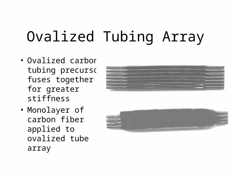
Ovalized Tubing Array
• Ovalized carbon tubing precursor fuses together for greater stiffness
• Monolayer of carbon fiber applied to ovalized tube array
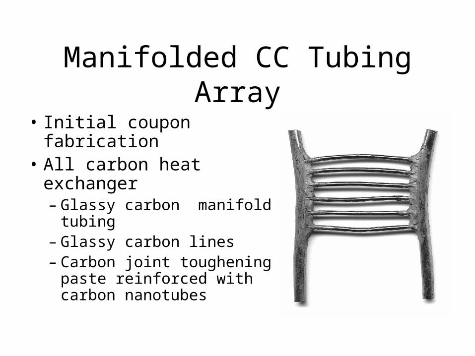
Manifolded CC Tubing Array
• Initial coupon fabrication• All carbon heat exchanger
– Glassy carbon manifold tubing
– Glassy carbon lines– Carbon joint toughening
paste reinforced with carbon nanotubes
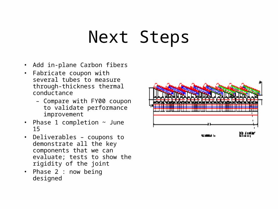
Next Steps
• Add in-plane Carbon fibers • Fabricate coupon with several
tubes to measure through-thickness thermal conductance – Compare with FY00 coupon to
validate performance improvement
• Phase 1 completion ~ June 15• Deliverables – coupons to
demonstrate all the key components that we can evaluate; tests to show the rigidity of the joint
• Phase 2 : now being designed
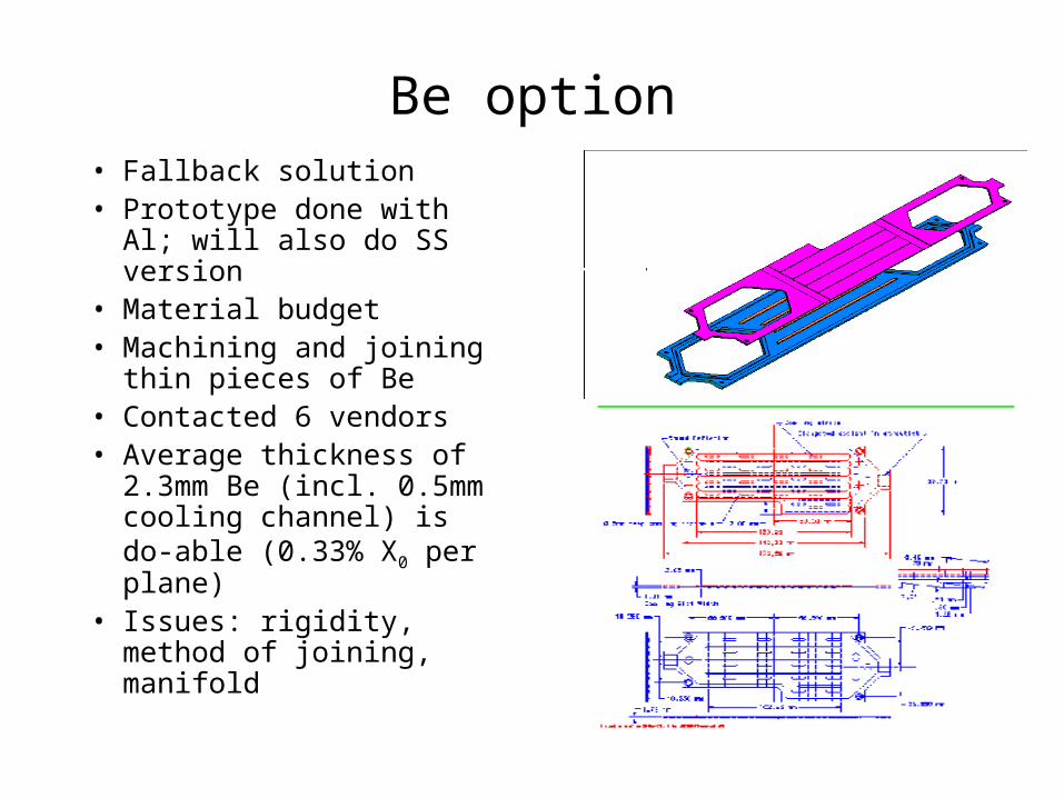
Be option• Fallback solution• Prototype done with Al;
will also do SS version• Material budget• Machining and joining
thin pieces of Be• Contacted 6 vendors• Average thickness of
2.3mm Be (incl. 0.5mm cooling channel) is do-able (0.33% X0 per plane)
• Issues: rigidity, method of joining, manifold
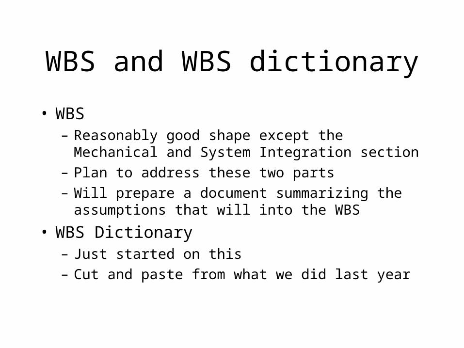
WBS and WBS dictionary
• WBS – Reasonably good shape except the Mechanical and
System Integration section
– Plan to address these two parts
– Will prepare a document summarizing the assumptions that will into the WBS
• WBS Dictionary– Just started on this
– Cut and paste from what we did last year
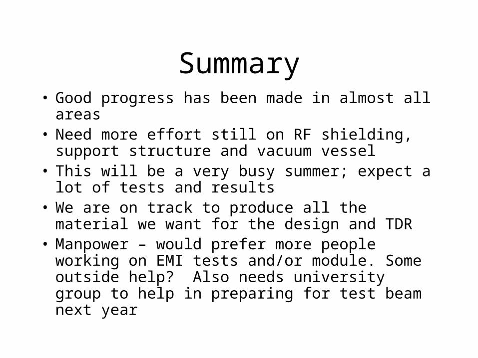
Summary• Good progress has been made in almost all areas• Need more effort still on RF shielding, support
structure and vacuum vessel• This will be a very busy summer; expect a lot of
tests and results• We are on track to produce all the material we
want for the design and TDR• Manpower – would prefer more people working
on EMI tests and/or module. Some outside help? Also needs university group to help in preparing for test beam next year