BTeV was terminated in February of 2005. BTeV Trigger.
38
BTeV was terminated in February of 2005. BTeV Trigger
-
date post
19-Dec-2015 -
Category
Documents
-
view
222 -
download
3
Transcript of BTeV was terminated in February of 2005. BTeV Trigger.

BTeV was terminated in February of 2005.
BTeV Trigger

BTeV Trigger Overview
• Trigger Philosophy: Trigger on characteristics common to all heavy-quark decays, separated production and decay vertices.
• Aim: Reject > 99.9% of background. Keep > 50% of B events.• The challenge for the BTeV trigger and data acquisition system
is to reconstruct particle tracks and interaction vertices in every beam crossing. Looking for topological evidence of B (or D) decay.
• This is feasible for BTeV detector and trigger system, because of – Pixel detector – low occupancy, excellent spatial resolution, fast readout
– Heavily pipelined and parallel architecture (~5000 processors)
– Sufficient memory to buffer events while awaiting trigger decision
– Rapid development in technology – FPGAs, processors, networking
• 3 Levels:– L1 Vertex trigger (pixels only) + L1 Muon trigger
– L2 Vertex trigger – refined tracking and vertexing
– L3 Full event reconstruction, data compression

BTeV detectorBTeV detector
pp
30 station

Multichip module
Si pixel detectorSi pixel detector
5 cm
1 cm
50 m
400 m Si pixel sensors
5 FPIX ROC’s
128 rows x22 columns
14,080 pixels (128 rows x 110 cols)
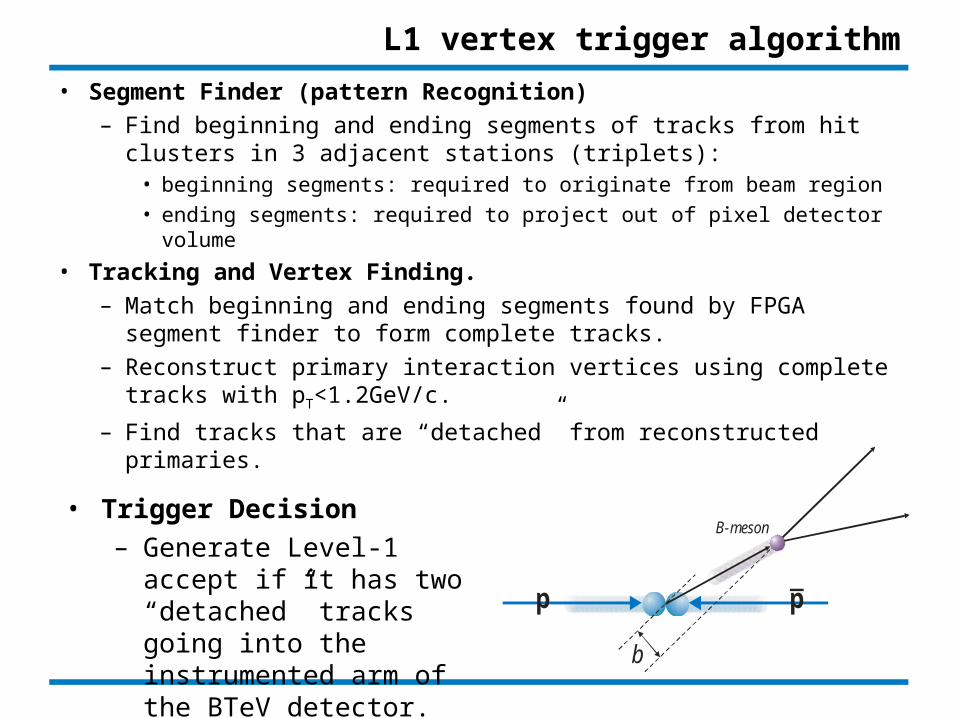
L1 vertex trigger algorithm
• Segment Finder (pattern Recognition)– Find beginning and ending segments of tracks from hit clusters
in 3 adjacent stations (triplets):• beginning segments: required to originate from beam region
• ending segments: required to project out of pixel detector volume
• Tracking and Vertex Finding.– Match beginning and ending segments found by FPGA segment
finder to form complete tracks. – Reconstruct primary interaction vertices using complete tracks
with pT<1.2GeV/c.
– Find tracks that are “detached” from reconstructed primaries.
b
p p
B-meson• Trigger Decision
– Generate Level-1 accept if it has two “detached” tracks going into the instrumented arm of the BTeV detector.
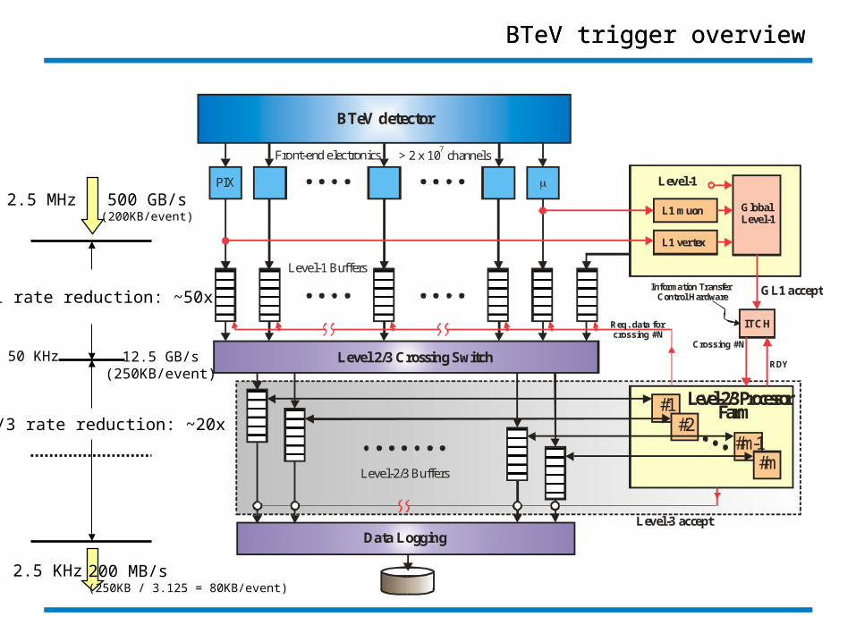
BTeV trigger overviewBTeV trigger overview
BTeV detector
L1 muon
L1 vertex
GlobalLevel-1
Level-1
Level 2/3 Crossing Switch
Data Logging
Front-end electronics
Level-1 Buffers
Level-2/3 Buffers
Information Transfer Control Hardware
ITCH
Level-2/3 Processor Farm#1
#2#m-1
#m
RDY
Crossing #N
Req. data for crossing #N
Level-3 accept
GL1 accept
PIX
> 2 x 10 channels7
500 GB/s(200KB/event)
2.5 MHz
L1 rate reduction: ~50x
L2/3 rate reduction: ~20x
12.5 GB/s(250KB/event)
50 KHz
2.5 KHz 200 MB/s(250KB / 3.125 = 80KB/event)
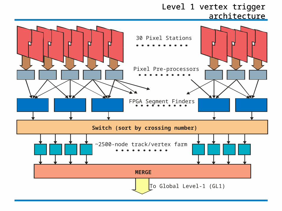
Level 1 vertex trigger architectureLevel 1 vertex trigger architecture
30 Pixel Stations
Pixel Pre-processors
FPGA Segment Finders
~2500-node track/vertex farm
Switch (sort by crossing number)
MERGE
To Global Level-1 (GL1)
Pixel PreprocessorCounting RoomCollision Hall
Pixel stations
FPIX2 Read-out chip
DCB
DCB
DCB
Data combiners
Row (7bits) Column (5bits) BCO (8bits) ADC (3bits)
sync (1bit)
Optical links
Pixelprocessor
Pixelprocessor
Pixelprocessor
Pixel processor
Optical Receiver Interface
Time Stamp Expansion
Event sorted by Time and column
Hit cluster finder & x-y coordinate translator
Level 1 Buffer
Interface
FPGAsegment finder
to neighboring FPGAsegment finder

The Segment Tracker Architecture
Long doublets
Triplets
N+1 Short doublets
N Short doublets
N-1 Short doublets
MUX
Station N Bend
Station N-1 Bend
Station N+1 BendLong doublet
projections
Triplets projection
Station N-1 nonbend
Station N nonbend
Triplets projection
Station N+1 nonbend
Triplets projection
Short doublet outputs
BB33 outputs
• Find interior and exterior track segments in parallel in FPGAs.
• The Segment finder algorithm is implemented in VHDL
Station 15
Station 16
Station 17
Station 15
Station 16
Station 17
Bend view
Nonbend view
12 half Pixel planes at 12 different Z locations.

L1 Track and Vertex Farm
• Original baseline of L1 track and vertex farm used custom made processor board based on DSP or other processors. Total processors estimated to be 2500 TI DSP 6711. The L1 switch is custom designed too.
• After DOE CD1 review, BTeV changed L1 baseline design. – L1 Switch, Commercial off-the-shell Infiniband switch
(or equivalent).– L1 Farm, array of commodity general processors,
Apple G5 Xserves (or equivalent).
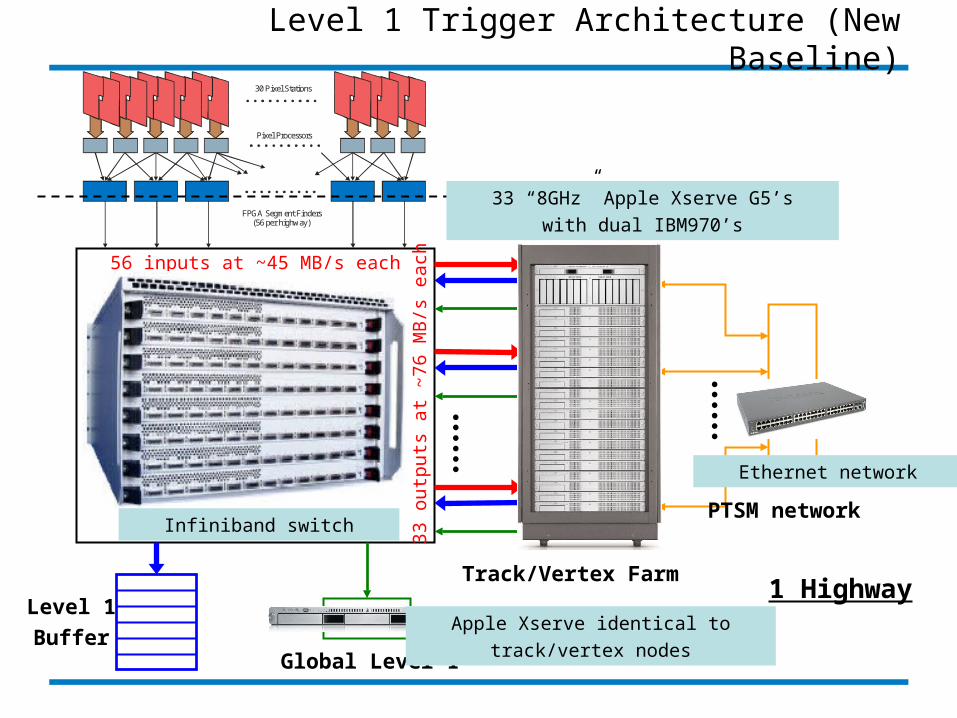
30 Pixel Stations
Pixel Processors
FPGA Segment Finders (56 per highway)
56 inputs at ~45 MB/s each
Level 1 switch33
out
puts
at
~76
MB
/s e
ach
1 Highway
Trk/Vtx
node #1
Trk/Vtx
node #2
Trk/Vtx
node #N PTSM network
Global Level 1
Level 1
Buffer
Track/Vertex Farm
33 “8GHz” Apple Xserve G5’s
with dual IBM970’s
Infiniband switch
Ethernet network
Apple Xserve identical to
track/vertex nodes
Level 1 Trigger Architecture (New Baseline)

R&D projects
• Software development for DSP Pre-prototype.• Level 1 trigger algorithm processing time studies on
various processors.– Part of trigger system R&D for a custom-made Level
1 trigger computing farm.• StarFabric Switch test and bandwidth measurement.
– R&D for new Level 1 Trigger system baseline design.– After DOE CD1 review, BTeV collaboration decided to
change baseline design of Level 1 trigger system. • L1 Switch – replace custom switch with Infiniband switch(or
equivalent).• L1 Farm – replace DSP hardware with Apple G5 Xserves (or
equivalent).
• Pixel Preprocessor of Level 1 trigger system.– Clustering algorithm and firmware development.

DSP Pre-prototype main goals
• Investigate current DSP hardware and software to determine technical choices for baseline design.
• Study I/O data flow strategies.• Study Control and Monitoring techniques.• Study FPGA firmware algorithms and simulation
tools.
– Understand major blocks needed.
– Estimate logic size and achievable data bandwidths.
• Measure internal data transfers rates, latencies, and software overheads between processing nodes.
• Provide a platform to run DSP fault tolerant routines.• Provide a platform to Run Trigger algorithms.

Features of DSP Pre-prototype Board
• Four DSP mezzanine cards on the board. This can test different Different TI DSPs for comparision.
• The FPGA Data I/O Manager provides two way data buffering. It Communicates the PCI Test Adapter (PTA ) card to each DSP.
• Two Arcnet Network ports.– Port I is the PTSM (Pixel Trigger Supervise Monitor). – Port II is the Global Level 1 result port. – Each Network port is managed by a Hitachi microcontroller. – PTSM microcontroller communicates to the DSPs via DSP Host
Interface to generate initialization and commands.– GL1 microcontroller receives trigger results via DSP’s Buffered
Serial Port (BSP).• Compact Flash Card to store DSP software and parameters.• Multiple JTAG ports for debugging and initial startup.• Operator LEDs.
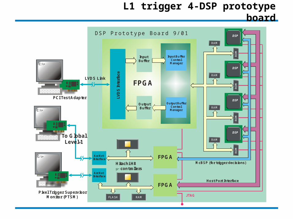
L1 trigger 4-DSP prototype board
C:\>
C:\>
DSP
DSP
DSP
DSP
Input Buffer Control Manager
Output Buffer Control Manager
InputBuffer
Output Buffer
LVD
S In
terf
ace
FPGA
FPGA
FPGA
Hitachi H8controllers
McBSP (for trigger decisions)
Host Port Interface
DSP
RO
M
JTAGFLASH RAM
ArcNetInterface
ArcNetInterface
LV
DS
Inte
rfac
e
LVDS Link
Pixel Trigger Supervisor Monitor (PTSM)
PCI Test Adapter
DSP P r ot o t y pe Boa r d 9/ 01
C:\>
To Global Level-1
RAM
RAM
RAM
RAM
RO
MR
OM
RO
M
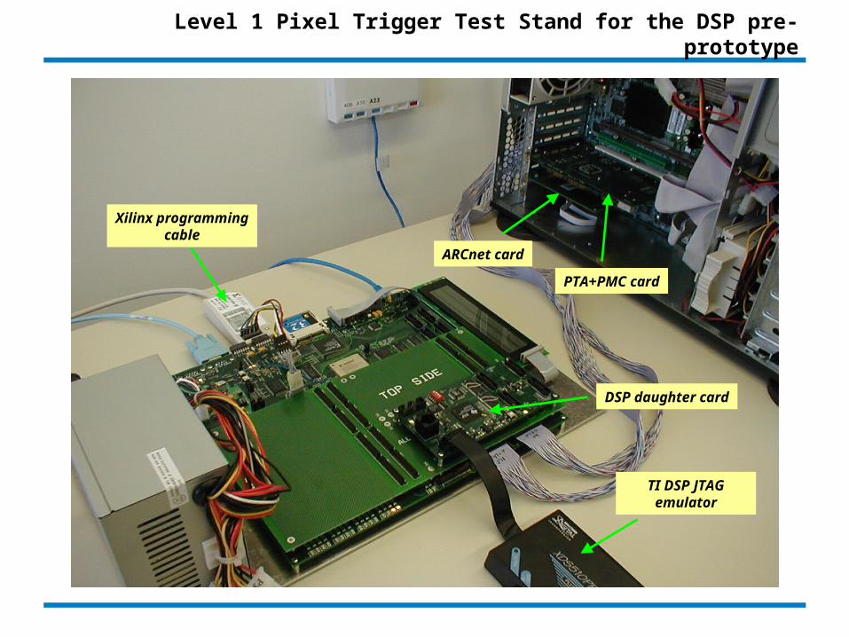
Level 1 Pixel Trigger Test Stand for the DSP pre-prototype
Xilinx programmingcable
PTA+PMC card
ARCnet card
TI DSP JTAG emulator
DSP daughter card
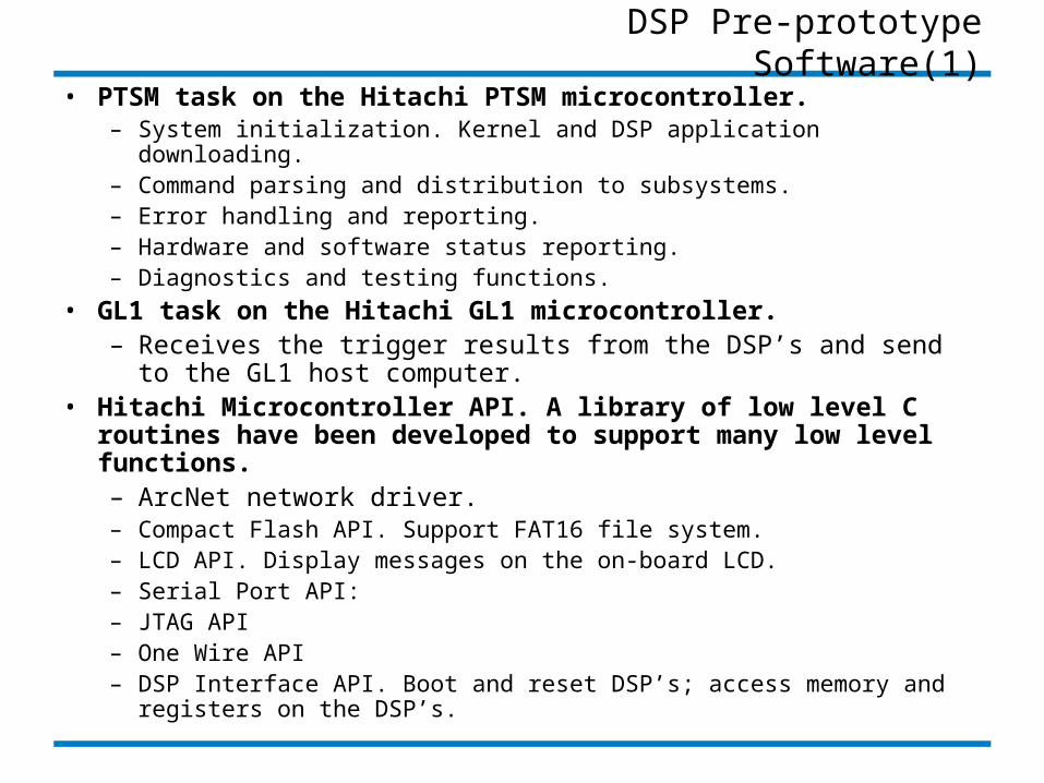
DSP Pre-prototype Software(1)
• PTSM task on the Hitachi PTSM microcontroller.– System initialization. Kernel and DSP application downloading.– Command parsing and distribution to subsystems. – Error handling and reporting.– Hardware and software status reporting.– Diagnostics and testing functions.
• GL1 task on the Hitachi GL1 microcontroller.– Receives the trigger results from the DSP’s and send to the GL1
host computer.• Hitachi Microcontroller API. A library of low level C routines
have been developed to support many low level functions.– ArcNet network driver.– Compact Flash API. Support FAT16 file system.– LCD API. Display messages on the on-board LCD.– Serial Port API:– JTAG API– One Wire API– DSP Interface API. Boot and reset DSP’s; access memory and registers
on the DSP’s.

DSP Pre-prototype Software(2)
• Host computer software. – PTSM Menu-driven interface.– GL1 message receiving and displaying.
• Custom defined protocol built on the lowest level of ArcNet network driver. Most efficient without standard protocol overhead.

Processor evaluation
• We continued to measure Level 1 trigger algorithm processing time on various new processors.
• MIPS RM9000x2 processor. Jaguar-ATX evaluation board.– Time studies on Linux 2.4– Time studies on standalone. Compiler MIPS SDE Lite 5.03.06.– System (Linux) overhead for processing time is about 14%.
• PowerPC 7447 (G4) and PowerPC 8540 PowerQuiccIII (G5).
– GDA Tech PMC8540 eval card and Motorola Sandpoint eval board with PMC7447A.
– Green Hills Multi2000 IDE with Green Hills probe for standalone testing.
Green Hills Probe
8540 eval board

Candidate processors for Level 1 Farm
Intel Pentium 4/Xeon
IBM 970 PPC
Motorola 74xx G4 PPC
Motorola 8540 PQIII PPC
PMC Sierra MIPS RM9000x2
L1 algorithm processing time
TI TMS320C6711 (baseline)
341 us (600MHz, MIPS SDE Lite 5.03.06)
195 us (1GHz 7455, Apple PowerMac G4)
117 us (2.4 GHz Xeon)
74 us (2.0 GHz Apple PowerMac G5)
1,571 us provided for comparison
suited for an off-the-shelf solution using desktop PC (or G5 server) for computing farm.
Processor
271 us (660MHz, GHS MULTI 2K 4.01)
Motorola 7447A G4 PPC 121 us (1.4GHz, GHS MULTI 2K 4.01)
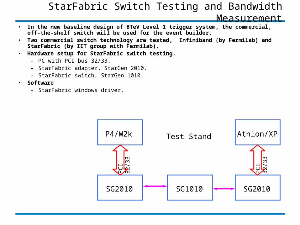
StarFabric Switch Testing and Bandwidth Measurement• In the new baseline design of BTeV Level 1 trigger system, the commercial, off-the-shelf
switch will be used for the event builder.• Two commercial switch technology are tested, Infiniband (by Fermilab) and StarFabric (by IIT
group with Fermilab).• Hardware setup for StarFabric switch testing.
– PC with PCI bus 32/33.– StarFabric adapter, StarGen 2010.– StarFabric switch, StarGen 1010.
• Software– StarFabric windows driver.
P4/W2k
SG2010
PC
I 32
/33
SG1010
Athlon/XP
SG2010
PC
I 32
/33
Test Stand

L1 Switch Bandwidth Measurement
• StarFabric bandwitdh is between 74~84 Mbytes/s for packet size of 1 kByte to 8 kBytes. This result can not meet the bandwidth requirement of event builder.
• A simple way to improve performance is to use PCI-x(32/66 or 64/66) . Infiniband test stand uses PCI-X adapters in input/output computer nodes.
• Based on this result and other consideration, Infiniband is chosen in the new baseline design of the Level 1 trigger system. But, we are still looking at StarFabric and other possible switch fabric.
167 MB/s Bandwidth Target
At peak luminosity (<6> ints./BCO),with 50% excess capacity
Infiniband
StarFabric

Pixel Preprocessor
Optical Receiver Interface
Time Stamp Expansion
Event sorted by Time and culomn
Hit cluster finder & x-y coordinate
translator
Segment Trackers
Pixel Detector Front-end
Level 1 Buffer
InterfaceDAQ
56 inputs at ~ 45 MB/s each
Level 1 switch
33 o
utpu
ts a
t ~
76 M
B/s
eac
h
Infiniband switch
30 station pixel detector
PP&STSegment Tracker Nodes
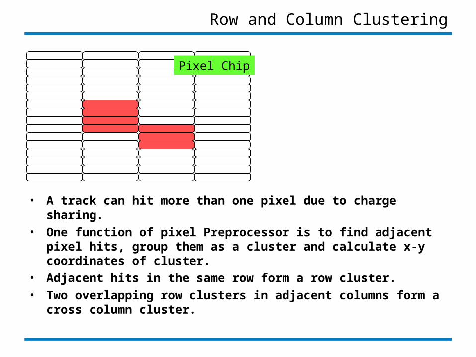
Row and Column Clustering
• A track can hit more than one pixel due to charge sharing.
• One function of pixel Preprocessor is to find adjacent pixel hits, group them as a cluster and calculate x-y coordinates of cluster.
• Adjacent hits in the same row form a row cluster.
• Two overlapping row clusters in adjacent columns form a cross column cluster.
Pixel Chip

Cluster Finder Block Diagram
• The order of input hits in a row is defined. However, the column order is not.
• The hash sorter is used to produce defined column order.
• The row cluster processor identifies adjacent hits in a row and pass the starting/ending row numbers to next stage.
• The cross-column processor groups overlap hits (or clusters) in adjacent columns together.
• Cluster parameters are calculated in the cluster parameter calculator.
Hit Input
Row Cluster Processor: Cross-Row Clusters
FIFO
Hash Sorter: Column Ordering
Cross-Column ProcessorCross-Col. Clusters
Col NCol N-1
Cluster ParametersCalculator
Cluster

Implementation for Cross-Column Cluster Finder
StateControl
Hits
Cross-rowheaders
Col. A
Col. B
Cross-columnheaders
Hits
Col. BCol. A
The cluster in Col. A is a single column one
and is popped out.
The two clusters form a cross-
column one and are popped out.
Col. BCol. A
If Col. B is not next to the Col. A, entire Col. A is popped out.
FIFO2
FIFO1
The cluster in Col. B is not connected with Col. A and is filled
into FIFO2.

Implementation for Cross-Column Cluster Finder (cont’d)
• The cross-column cluster finder firmware is written with VHDL.
Fill Col. A
Col. B = Col. A +1 ?
Pop Col. AFill Col. B
(1) uAN< uB1
(2) uA1 > uBN
Fill BPop A Pop APop B
Y
N
uAN< uB1 uA1 > uBN
Neither
StateControl
Col. A
Col. B
FIFO2
FIFO1
BES-II DAQ System
BES experiment upgraded its detector and DAQ system in 1997.

Beijing Spectrometer
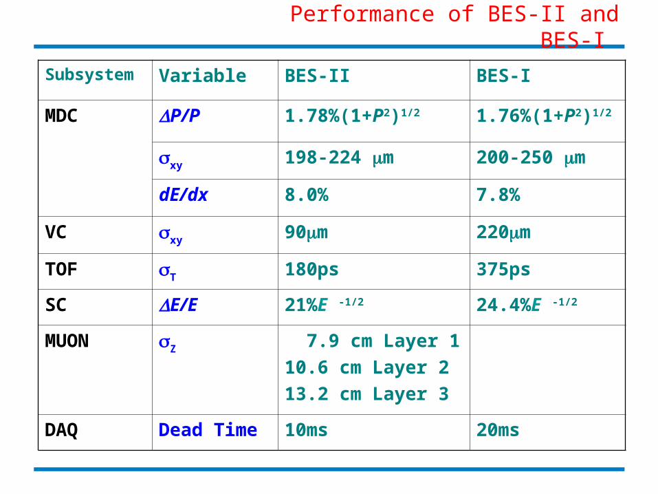
Performance of BES-II and BES-I
Subsystem Variable BES-II BES-I
MDC P/P 1.78%(1+P2)1/2 1.76%(1+P2)1/2
xy 198-224 m 200-250 m
dE/dx 8.0% 7.8%
VC xy 90m 220m
TOF T 180ps 375ps
SC E/E 21%E -1/2 24.4%E -1/2
MUON Z 7.9 cm Layer 1
10.6 cm Layer 2
13.2 cm Layer 3
DAQ Dead Time 10ms 20ms

BES-II DAQ System• Front-end electronics for all of system,
except VC, consist of CAMAC BADC (Brilliant ADC).
• VCBD, VME CAMAC Branch Driver. Read data of one detector subsystem. And store the data in the local buffer.
• Two VME CPU modules with RT OS VMEexec.
– One for data acquisition and event building.
– Another one for event logging to tape and sending a fraction of events to Alpha 3600.
• DEC Alpha 3600 machine. – DAQ control console.– Status/error report. – Online data analysis and display.– Communication with BEPC control
machines to obtain BEPC status parameters.
• The system dead time: 10 ms.– BADC conversion: 6ms.– VCBD readout: 3ms.
ALPHA 3600 ServerOPEN VMS
VME BUS
VME BUS
VME 167HOST
VME 162Target 2
VME 162Target 1
VMEMemery
VCBD 0 VCBD1 VCBD2 VCBD3 VCBD4 VCBD5 VCBD6 VCBD7 VCBD81131
1821
VC 1879 TDC
BESControl
VMEBusRepeater
VMEBusRepeater
SCSI BUS
DISK 8mm Tape
Ethernet
C A M A C
MDC-Q TRGMDC-T H.V.LUMESCBSCMUONTOF
FASTBUS

Fastbus subsystem for Vertex Chamber
• One Fastbus crate for 640 VC channels.
• Fastbus logical board.– Distributes every kind
of signals to TDCs, common stop, reset (fast clear).
– Produce internal start and stop test pulses.
– Good event signal tells the 1821 to read data from 1879.
1879TDC
1879TDC
1821SM/I
logicalboard
PC
1131
VME162
VME162
commonstop
goodevent
reset
FASTbus
VME bus
SIB
ECL INPUT

Microcode for the 1821
• Initialization for 1879.
– TDC scale: 1 us.
– Compact parameter: 10 ns.
– Active Time Interval: 512 bins.
• Readout 1879 data into data memory of 1821.
– Block transfer.
– Sparse data scan method. TDC modules containing data are readout only.
• Send data ready signal (interrupt) to VME.
• SONIC language. Symbolic Macro Assembler. Converted to microcode under LIFT.
• LIFT (LeCroy Interactive Fastbus Toolkit). Tool for developing microcodes and testing FB system under PC.
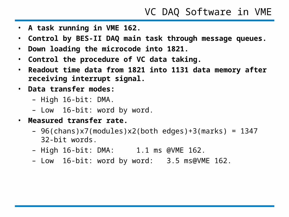
VC DAQ Software in VME
• A task running in VME 162.
• Control by BES-II DAQ main task through message queues.
• Down loading the microcode into 1821.
• Control the procedure of VC data taking.
• Readout time data from 1821 into 1131 data memory after receiving interrupt signal.
• Data transfer modes:
– High 16-bit: DMA.
– Low 16-bit: word by word.
• Measured transfer rate.
– 96(chans)x7(modules)x2(both edges)+3(marks) = 1347 32-bit words.
– High 16-bit: DMA: 1.1 ms @VME 162.
– Low 16-bit: word by word: 3.5 ms@VME 162.

End
The End

Backup slides
Backups
GlobalLevel-1
ITCH
Information Transfer Control Hardware
GL1
Level-1 Buffers
12 x 24-port Fast Ethernet Switches
Level 2/3Processor Farm
Pixel Processors
FPGA Segment Finder
Track/Vertex Farm
Gigabit Ethernet Switch
Data Combiners +Optical Transmitters
OpticalReceivers
BTeV Detector
Front End Boards
8 Data Highways
Data Logger
Cross Connect Switch
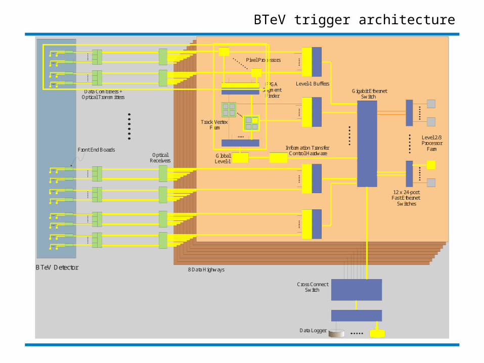
BTeV trigger architecture

L1 Highway Bandwidth Estimates
WorkerNode
GL1 + ITCHNode
L2 Node
SegmentTrackerNode
SegmentTracker Node
~30
~15
~96
Total Triplets 2.5GB/s
Other: 10MB/s (Raw Pixel Data)
Switching Fabric
WorkerNode
WorkerNode
DAQ Switch
L2 Node
SegmentTracker Node
167 MB/s
83 MB/s
15 MB/s
1.8 MB/s + 0.5 MB/s
Bridge
300 KB/s
L2 Node
L1 Buffers
L1 Buffers
L1 Buffers
Muons
Front Ends
Results+Triplets 54 MB/s
(1/50 rejection)Other: 1 GB/s
Results+Triplets 583 KB/s
Bandwidth estimates are for 6
interactions/crossing & include 50 % excess capacity
DAQ Highway Switch