PACKAGE-ON-PACKAGE INTERCONNECT FOR FAN-OUT WAFER … · 1 PACKAGE-ON-PACKAGE INTERCONNECT FOR...
39
1 PACKAGE-ON-PACKAGE INTERCONNECT FOR FAN-OUT WAFER LEVEL PACKAGES Min Tao, Ph. D, Ashok Prabhu, Akash Agrawal, Ilyas Mohammed, Ph. D, Bel Haba, Ph. D Oct 18-20 2016, IWLPC
Transcript of PACKAGE-ON-PACKAGE INTERCONNECT FOR FAN-OUT WAFER … · 1 PACKAGE-ON-PACKAGE INTERCONNECT FOR...

1
PACKAGE-ON-PACKAGE INTERCONNECT
FOR FAN-OUT WAFER LEVEL PACKAGESMin Tao, Ph. D, Ashok Prabhu, Akash Agrawal,
Ilyas Mohammed, Ph. D, Bel Haba, Ph. D
Oct 18-20 2016, IWLPC

2 Oct 18-20, 2016 IWLPC
Laminate to Fan-Out WLP Transition
FOWLP POP Key Elements
POP Interconnect Features
Conclusion
Outline

3 Oct 18-20, 2016 IWLPC
Laminate to Fan-Out WLP Transition
FOWLP POP Key Elements
POP Interconnect Features
Conclusion
Outline

4 Oct 18-20, 2016 IWLPC
Fan-Out Evolution
Evolving
10100um 10um
~ 8 – 2um
2um
Substrate design Rule
OSAT / wafer foundries
Opportunity area for
wafer/panel level Fan-Out
solutions

5 Oct 18-20, 2016 IWLPC
Package Stacking Transitioning
PIP
Redistributed
bonding pads
2.5D stacking with
mostly wirebond
based approach

6 Oct 18-20, 2016 IWLPC
Package Stacking Transitioning
Laminate POP
Solder only
BVA
TMVWarpage control
Finer POP pitch
1st Gen POP
PIP
Redistributed
bonding pads
2.5D stacking with
mostly wirebond
based approach

7 Oct 18-20, 2016 IWLPC
Package Stacking Transitioning
Laminate POP
Solder only
BVA
TMVWarpage control
Finer POP pitch
1st Gen POP
FOWLP POP
Chip lastWafer Level process
replacing laminate substrate
with thinner RDLs
Chip firstAchieving lowest stack
profile with improved
performance with RDLs
built directly on chip
PIP
Redistributed
bonding pads
2.5D stacking with
mostly wirebond
based approach
8 Oct 18-20, 2016 IWLPC
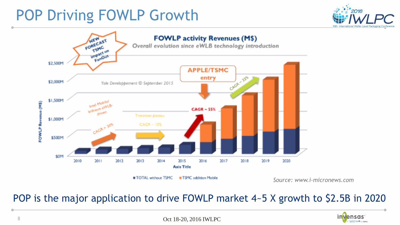
POP Driving FOWLP Growth
POP is the major application to drive FOWLP market 4~5 X growth to $2.5B in 2020
Source: www.i-micronews.com
9 Oct 18-20, 2016 IWLPC
Laminate to Fan-Out WLP Transition
FOWLP POP Key Elements
POP Interconnect Features
Conclusion
Outline

10 Oct 18-20, 2016 IWLPC
FOWLP POP Key Ingredients
FOWLP

11 Oct 18-20, 2016 IWLPC
FOWLP POP Key Ingredients
FOWLP
Manufacturing
: Panel OR
wafer

12 Oct 18-20, 2016 IWLPC
FOWLP POP Key Ingredients
FOWLP
Manufacturing
: Panel OR
waferChip: First
(face up OR
face down) OR
Last

13 Oct 18-20, 2016 IWLPC
FOWLP POP Key Ingredients
FOWLP
Manufacturing
: Panel OR
wafer
Vias: Formed
post mold OR
Preformed
Chip: First
(face up OR
face down) OR
Last

14 Oct 18-20, 2016 IWLPC
FOWLP POP Key Ingredients
FOWLP
Manufacturing
: Panel OR
wafer
1st side
RDL(s): after
molding OR
before molding
on a carrier
2nd side
RDL:
if needed
Vias: Formed
post mold OR
Preformed
Chip: First
(face up OR
face down) OR
Last

15 Oct 18-20, 2016 IWLPC
FOWLP POP Key Ingredients
FOWLP
Manufacturing
: Panel OR
wafer
1st side
RDL(s): after
molding OR
before molding
on a carrier
2nd side
RDL:
if needed
Vias: Formed
post mold OR
Preformed
Chip: First
(face up OR
face down) OR
Last
Molding

16 Oct 18-20, 2016 IWLPC
FOWLP POP Key Ingredients
FOWLP
Manufacturing
: Panel OR
wafer
1st side
RDL(s): after
molding OR
before molding
on a carrier
2nd side
RDL:
if needed
Vias: Formed
post mold OR
Preformed
Chip: First
(face up OR
face down) OR
Last
Molding
Reliability: copper bumped
die OR thick
dielectric added

17 Oct 18-20, 2016 IWLPC
FOWLP POP Key Ingredients
FOWLP
Manufacturing
: Panel OR
wafer
1st side
RDL(s): after
molding OR
before molding
on a carrier
2nd side
RDL:
if needed
Vias: Formed
post mold OR
Preformed
Chip: First
(face up OR
face down) OR
Last
Molding
Reliability: copper bumped
die OR thick
dielectric added
eWLB POP
SLIM/SWIFT
BEOL/RDL

18 Oct 18-20, 2016 IWLPC
Chip First Facing Down: eWLB POP
Source: S. W. Yoon et. al., IWLPC, 2011

19 Oct 18-20, 2016 IWLPC
Chip First Facing Down: eWLB POP
eWLBPOP
Manufacturing
: wafer
1st side
RDL(s): after
molding
2nd side
RDL:
No
Vias:
preformed
(embedded PCB
vias)
Chip: First
face down)
Molding
Reliability: thick dielectric
added
Source: S. W. Yoon et. al., IWLPC, 2011

20 Oct 18-20, 2016 IWLPC
Chip First Facing Down: eWLB POP
eWLBPOP
Manufacturing
: wafer
1st side
RDL(s): after
molding
2nd side
RDL:
No
Vias:
preformed
(embedded PCB
vias)
Chip: First
face down)
Molding
Reliability: thick dielectric
added
Source: S. W. Yoon et. al., IWLPC, 2011
eWLB POP:
• Chip first, face down; RDL L/S 10/10um;
• Preformed vias by embedding laminate PCB with through-vias;
• Min via pitch ~ 0.27mm

21 Oct 18-20, 2016 IWLPC
Chip First Facing Up : InFO POP
Source: C.F. Tseng, et. al., ECTC 2016
Source: System Plus Consulting

22 Oct 18-20, 2016 IWLPC
Chip First Facing Up : InFO POP
Source: C.F. Tseng, et. al., ECTC 2016
Source: System Plus Consulting
InFOPOP
Manufacturing
: wafer
1st side
RDL(s): after
molding
2nd side
RDL:
PI only
Vias: preformed
(plated Cu pillars)
Chip: First
face Up)
Molding
Reliability: Tall Cu pads
and thick
dielectric added

23 Oct 18-20, 2016 IWLPC
Chip First Facing Up : InFO POP
Source: C.F. Tseng, et. al., ECTC 2016
Source: System Plus Consulting
InFOPOP
Manufacturing
: wafer
1st side
RDL(s): after
molding
2nd side
RDL:
PI only
Vias: preformed
(plated Cu pillars)
Chip: First
face Up)
Molding
Reliability: Tall Cu pads
and thick
dielectric added
InFO POP:
• Chip first, face up; 1 Fan-in RDL + 3 Fan-out RDL;
• Preformed vias by plated Cu pillars;
• Via pitch 300um (could be as low as 60um)

24 Oct 18-20, 2016 IWLPC
Chip Last: SWIFT and SLIM
Source: Amkor White Paper

25 Oct 18-20, 2016 IWLPC
Chip Last: SWIFT and SLIM
Source: Amkor White Paper
SWIFT/SLIM
Manufacturing
: wafer
1st side
RDL(s): before
molding
2nd side
RDL:
No
Vias: Postformed
(TMV)
Chip: Last
(flip chip)
Molding
Reliability: Flip chip

26 Oct 18-20, 2016 IWLPC
Chip Last: SWIFT and SLIM
Source: Amkor White Paper
SWIFT/SLIM
Manufacturing
: wafer
1st side
RDL(s): before
molding
2nd side
RDL:
No
Vias: Postformed
(TMV)
Chip: Last
(flip chip)
Molding
Reliability: Flip chip
SLIM and SWIFT:
• Chip last with a flip chip reflow step; Finer L/S with SLIM BEOL layers;
• TMV like via by laser opening; Min Via pitch ~ 0.30mm

27 Oct 18-20, 2016 IWLPC
Laminate to Fan-Out WLP Transition
FOWLP POP Key Elements
POP Interconnect Features
Conclusion
Outline

28 Oct 18-20, 2016 IWLPC
Chip Last Process Flow with Preformed Vias
1, Carrier wafer/panel with release tape
Release tape
RDL Passivation UBMC4 PadPOP Pad
2, Build up RDL (second level UBM
-> RDL -> C4 & POP pads)
4, Flip chip attach dies with solder on
pads, reflow to make joints
Die SoD
Preformed Vias (BVA or etched)
3, Preform POP Vias on the
wafer/panel (wire bond, etched, etc.)
5, Overmold to cover die and POP Vias
6, Grind back the mold to reveal the
Via pads; optional 2nd side RDL
7-9, Remove carrier wafer/panel;
Ball attach; singulation
Final Package – with 2nd side RDL
Fan-in RDL pads for POP connectivity

29 Oct 18-20, 2016 IWLPC
Preformed Vias – Etched Cu uPILR ®
uPILR® is a scalable Fine Pitch Interconnect
Technology with etched Cu post, suitable for
POP, flip chip and BGA
Etched Cu
uPILR®
Pillar on Substrate After stacking
uPILR POP:
- Batch process fine pitch interconnect, min Pitch 150~200um
- Good wetting and self-alignment capability for solder reflow
- Superior drop and T/C performance compared to BGA
An earlier uPILR
POP implementation

30 Oct 18-20, 2016 IWLPC
Preformed Vias – BVA®
BVA® is a Very Fine Pitch Vertical Wirebond
Interconnect Technology, ideal for POPBVA® Vertical
Interconnects
BVA POP:
- Utilize existing wire bond facilities
- Fine pitch capability of 150um
- Validated HVM feasibility with a Tier 1 OSAT

31 Oct 18-20, 2016 IWLPC
BVA on RDL Bondability Study
JEDEC Requirement
All test legs passed JEDEC ball shear requirement with high margin
BVA shows good bondability on RDL
Ack: Tong Hsing Electronics
TV: 10um PI with 5um Cu pad on 4” wafer

32 Oct 18-20, 2016 IWLPC
Cost Comparison
Sequential process has cost advantage up to ~800 IOs per package (15x15mm WLP on 12 inch wafer, all with 200um tall interconnect)
Ack: Savansys Solutions
0
0.5
1
1.5
2
2.5
3
200 400 600 800 1000 1200
Co
st P
er
Inte
rco
nn
ect
(N
orm
aliz
ed
)
Estimated # of POP IO per 15X15mm WLP
Plated Cu Pillar
BVA Wire
Laser Drilled TMV
Pitch
~0.16mm
Pitch
~0.2mm
Pitch
~0.3mm

33 Oct 18-20, 2016 IWLPC
Interconnect Technology Comparison
Chip first,
face up
Chip first,
face downChip last
Backside
RDL
BVA Wires/ Etched
Cu postsX X X 0.15mm
Plated Cu Pillars X X X 0.06mm-
Through Mold Lased
ViasX 0.30mm
Solder balls X 0.4mm+
PCB Through-Vias X X X 0.27mm
Compatibility ("X" for compatible)
POP Interconnect Min Pitch

34 Oct 18-20, 2016 IWLPC
eWLB POP InFO SLIM/SWIFT uPILR/BVA
Process flow Chip (face down)
Interconnect (PCB
through-Vias)
RDL
Interconnect (Plated Cu
pillar)
Chip (face up)
RDL
BEOL/RDL
Chip (flip chip)
Interconnect (TMV)
RDL/ Laminate
Interconnect (etched Cu
pillar, vertical BVA)
Chip (flip chip)
Features - Mature FOWLP
process;
- Thinnest POP in
market;
- Finest POP pitch
- Fine L/S (BEOL);
- Chip last
- Preformed POP Vias at
fine pitch;
- Process yield and
reliability
Limitations - Coarse POP pitch;
- Process/material
complexity
- Package cost
- Warpage
- Package cost
- Thickness
- BVA Sequential
process;
- Infrastructure
compatibility
FOWLP POP Comparison

35 Oct 18-20, 2016 IWLPC
Conclusion
• Laminate to Fan-Out WLP Transition
POP SoC requirement of IO density, thickness, and L/S drives transition
to FOWLP

36 Oct 18-20, 2016 IWLPC
Conclusion
• Laminate to Fan-Out WLP Transition
POP SoC requirement of IO density, thickness, and L/S drives transition
to FOWLP
• FOWLP POP Key Elements
Main distinguishing feature among FOWLP approaches is Chip first or
Chip last, which impacts cost and yield
37 Oct 18-20, 2016 IWLPC
Conclusion
• Laminate to Fan-Out WLP Transition
POP SoC requirement of IO density, thickness, and L/S drives transition
to FOWLP
• FOWLP POP Key Elements
Main distinguishing feature among FOWLP approaches is Chip first or
Chip last, which impacts cost and yield
• POP Interconnect Features
Cu post offers finest pitch and thinnest package
BVA and uPILR are fine pitch alternatives utilizing existing assembly
infrastructure

38 Oct 18-20, 2016 IWLPC
• Tong Hsing Electronics for bondability study
• Savansys Solutions for BVA cost analysis
• Hala Shaba and Rajesh Katkar from Invensas team for FA support
Acknowledgement