A Cost-Effective Approach for Wafer Level Chip Scale ... Cost-Effective Approach for Wafer Level...
31
June 3 June 3 - - 6, 2007 6, 2007 San Diego, CA USA San Diego, CA USA A Cost-Effective Approach for Wafer Level Chip Scale Package Testing Norman J. Armendariz, PhD Texas Instruments, Inc
Transcript of A Cost-Effective Approach for Wafer Level Chip Scale ... Cost-Effective Approach for Wafer Level...

June 3June 3--6, 20076, 2007San Diego, CA USASan Diego, CA USA
A Cost-Effective Approach for Wafer Level Chip Scale Package Testing
Norman J. Armendariz, PhDTexas Instruments, Inc

June 3-6, 2007June 3June 3--6, 20076, 2007 IEEE SW Test WorkshopIEEE SW Test WorkshopIEEE SW Test Workshop 222
AGENDA• The Need• WSP-Wafer Scale Packages• WSP- Manufacturing Test Flow• WSP Probe Card Technologies• Challenges• Comparative Summary• Discussion

June 3-6, 2007June 3June 3--6, 20076, 2007 IEEE SW Test WorkshopIEEE SW Test WorkshopIEEE SW Test Workshop 333
THE NEED
TI has been testing packages at final test after singulation for some time. However, the increasing use of WLCSP- wafer level chip scale package formats require cost-effective RF testing at the wafer-level or before singulation to further reduce test costs and be globally competitive.
June 3-6, 2007June 3June 3--6, 20076, 2007 IEEE SW Test WorkshopIEEE SW Test WorkshopIEEE SW Test Workshop 444
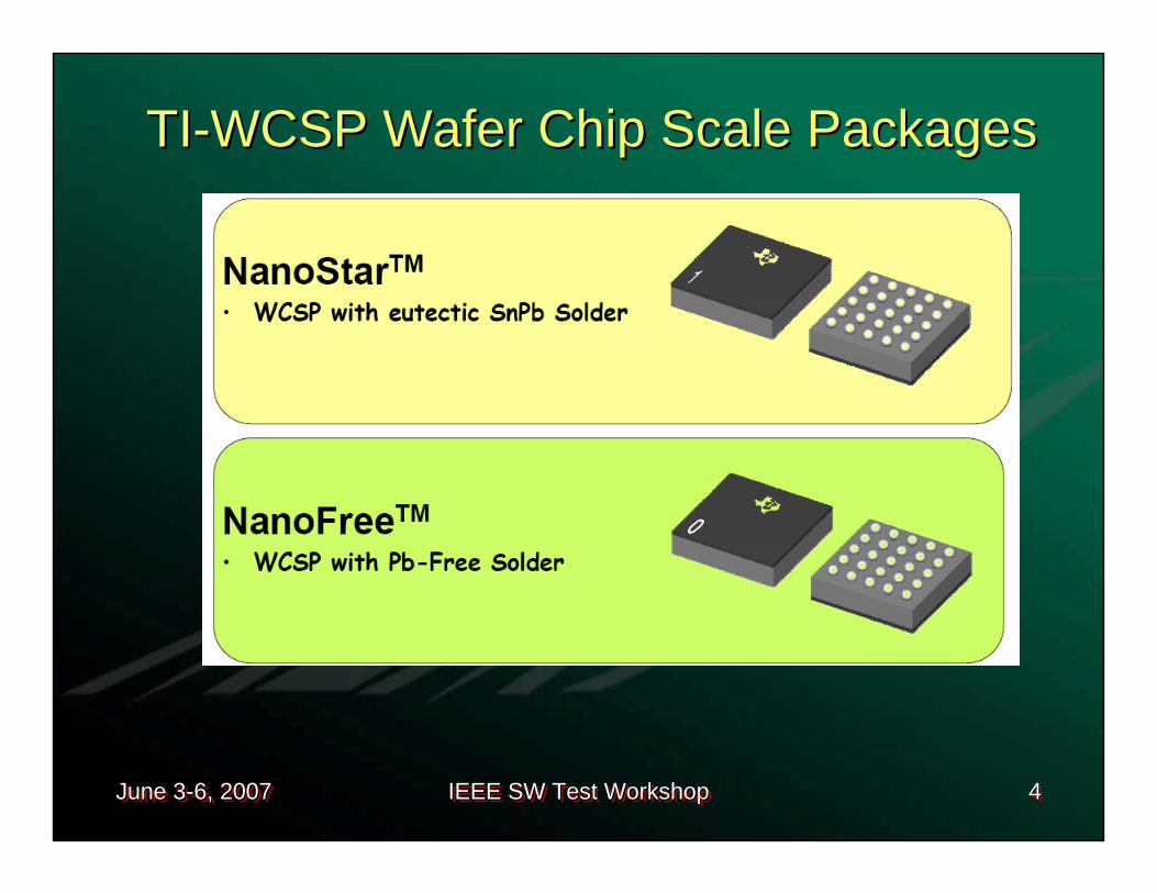
TITI--WCSP Wafer Chip Scale PackagesWCSP Wafer Chip Scale Packages

June 3-6, 2007June 3June 3--6, 20076, 2007 IEEE SW Test WorkshopIEEE SW Test WorkshopIEEE SW Test Workshop 555
WCSP- Redistribution Layer-RDL
Image Courtesy of the Tucson Reliability Test Lab
SEM VIEW
OM VIEW
XS VIEW
Bump
PI2
NitridePI1
Al
Silicon
BUMP
RDL UBM
Silicon

June 3-6, 2007June 3June 3--6, 20076, 2007 IEEE SW Test WorkshopIEEE SW Test WorkshopIEEE SW Test Workshop 666
WLCSP w/ RDL Examples

June 3-6, 2007June 3June 3--6, 20076, 2007 IEEE SW Test WorkshopIEEE SW Test WorkshopIEEE SW Test Workshop 777
WSP Test Flow -SimplifiedWafer
Fab
Wafer Probe(Functional)
RDL/Bump (AOI)
BackgrindWafer Probe
RF TestWafer Mount/Saw
AssemblyRF Test
(Sample Burn-in)
Backgrind
Inspection
Laser Mark
T&R/Tray
Wafer Mount/SawInspectionT&R / WP
Final Test WSP

June 3-6, 2007June 3June 3--6, 20076, 2007 IEEE SW Test WorkshopIEEE SW Test WorkshopIEEE SW Test Workshop 888
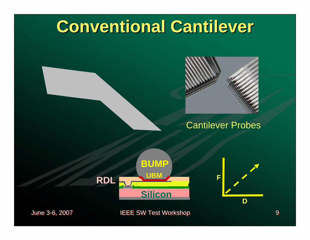
• Cantilever- (Needle Probes)• Vertical- (Buckling Beam) • Membrane (Beam Probes) RF
Current Wafer Level Probe Card Technologies
June 3-6, 2007June 3June 3--6, 20076, 2007 IEEE SW Test WorkshopIEEE SW Test WorkshopIEEE SW Test Workshop 999
Conventional Cantilever Conventional Cantilever
F
D
Cantilever Probes
Bump
PI2
NitridePI1
Al
Silicon
BUMP
RDL UBM
Silicon

June 3-6, 2007June 3June 3--6, 20076, 2007 IEEE SW Test WorkshopIEEE SW Test WorkshopIEEE SW Test Workshop 101010
Vertical Vertical Buckling Buckling
BeamBeam
F
D
Ceramic
Ceramic
Ceramic
Mylar
Buckling Beam Probes
Bump
PI2
NitridePI1
Al
Silicon
BUMP
RDL UBM
Silicon

June 3-6, 2007June 3June 3--6, 20076, 2007 IEEE SW Test WorkshopIEEE SW Test WorkshopIEEE SW Test Workshop 111111
Membrane RF Membrane RF Probe BeamsProbe Beams
F
D
Probe Beams
Bump
PI2
NitridePI1
Al
Silicon
BUMP
RDL UBM
Silicon

June 3-6, 2007June 3June 3--6, 20076, 2007 IEEE SW Test WorkshopIEEE SW Test WorkshopIEEE SW Test Workshop 121212
WSP Probe Card Tech ApplicabilityBoth cantilever and VPC probe cards exhibited limited electrical properties as well as other physical & operational limitations and can reach 0.3mm but require a space transformer, i.e., MLC/MLO to PCB.
Membrane probe cards have been employed for FC applications that need controlled impedance for RF (radio frequency) testing and can easily reach 0.3mm, but at some cost and also with deflection/ compliance limitations.
Current WLCSP FT-final test contactor technologies, which already use similar sockets and RF pogo pins, so that a similar approach can be also used in wafer level probe card form is the preferred cost-effective approach, to avoid an expensive probe card and skip the RF FT step.

June 3-6, 2007June 3June 3--6, 20076, 2007 IEEE SW Test WorkshopIEEE SW Test WorkshopIEEE SW Test Workshop 131313
Vertical RF Vertical RF PogoPogo--PinPin
F
D
RF Pogo Pins
Bump
PI2
NitridePI1
Al
Silicon
BUMP
RDL UBM
Silicon

June 3-6, 2007June 3June 3--6, 20076, 2007 IEEE SW Test WorkshopIEEE SW Test WorkshopIEEE SW Test Workshop 141414

June 3-6, 2007June 3June 3--6, 20076, 2007 IEEE SW Test WorkshopIEEE SW Test WorkshopIEEE SW Test Workshop 151515
WSP Probe Card Integration Challenges• Probe to Bump Interaction (OT, Alignment)• Prober/tester Mechanical Interface
(Components, Deflection)• Prober/PCB/Socket/Pogo-Pin and Bump
Planarity (Net Compliance, Bump Hts Vary) • Socket/ Pogo-Pin Design (RF, Tip Shape)• Alignment Algorithm (Auto Z-Ht Control)• Cleaning (Media, Stepping, CRes)• Thermal Requirements (-40 to 129C)• Industry Maturity (Supplier Base)

June 3-6, 2007June 3June 3--6, 20076, 2007 IEEE SW Test WorkshopIEEE SW Test WorkshopIEEE SW Test Workshop 161616
Probe to Bump Interaction
Pogo-pogo tip morphology, planarity and alignment critical to control amount of over-drive. For example, a 4-pt Crown tip uniformly distributes the force (L) as compared to when only 1 of 4 tips contacting, showing more bump deformation “gouging” as a result (R).

June 3-6, 2007June 3June 3--6, 20076, 2007 IEEE SW Test WorkshopIEEE SW Test WorkshopIEEE SW Test Workshop 171717
WSP Probe Card Design
Wafer Side Insulator Wafer Side-Keep-out Areas
Wafer side (L) and “blue” insulator (R) overlaid as a template showing exposed areas that are allowed between probe card and probe card support plate for components. With a maxheight (Z) of 0.040” allowed for this tester interface configuration.

June 3-6, 2007June 3June 3--6, 20076, 2007 IEEE SW Test WorkshopIEEE SW Test WorkshopIEEE SW Test Workshop 181818
Wafer Side Component Interference
• Jumper “Blue Wires”• Through-Hole-Mount Solder Joints• LED Components • PCB Barrel Vias Protruding• Sockets and/or Pogo Pins Heights

June 3-6, 2007June 3June 3--6, 20076, 2007 IEEE SW Test WorkshopIEEE SW Test WorkshopIEEE SW Test Workshop 191919
Tester Side Component Interference
Tester Side- Planarization Ring Location RASP Pogo Pin Tower- Outer Ring
Components as located would interfere with interface tester features such as an “inner” ring (red circle) on PCB tester side (L) to Tester pogo-pin outer ring array on tester tower (R).

June 3-6, 2007June 3June 3--6, 20076, 2007 IEEE SW Test WorkshopIEEE SW Test WorkshopIEEE SW Test Workshop 202020
WSP Probe Card RF Pogo Pin QS
Wafer Side Tester Side
Probe Head Probe Head
PCB 4-DUT Probe Head
Sockets / Pogo-Pins 1x4
June 3-6, 2007June 3June 3--6, 20076, 2007 IEEE SW Test WorkshopIEEE SW Test WorkshopIEEE SW Test Workshop 212121
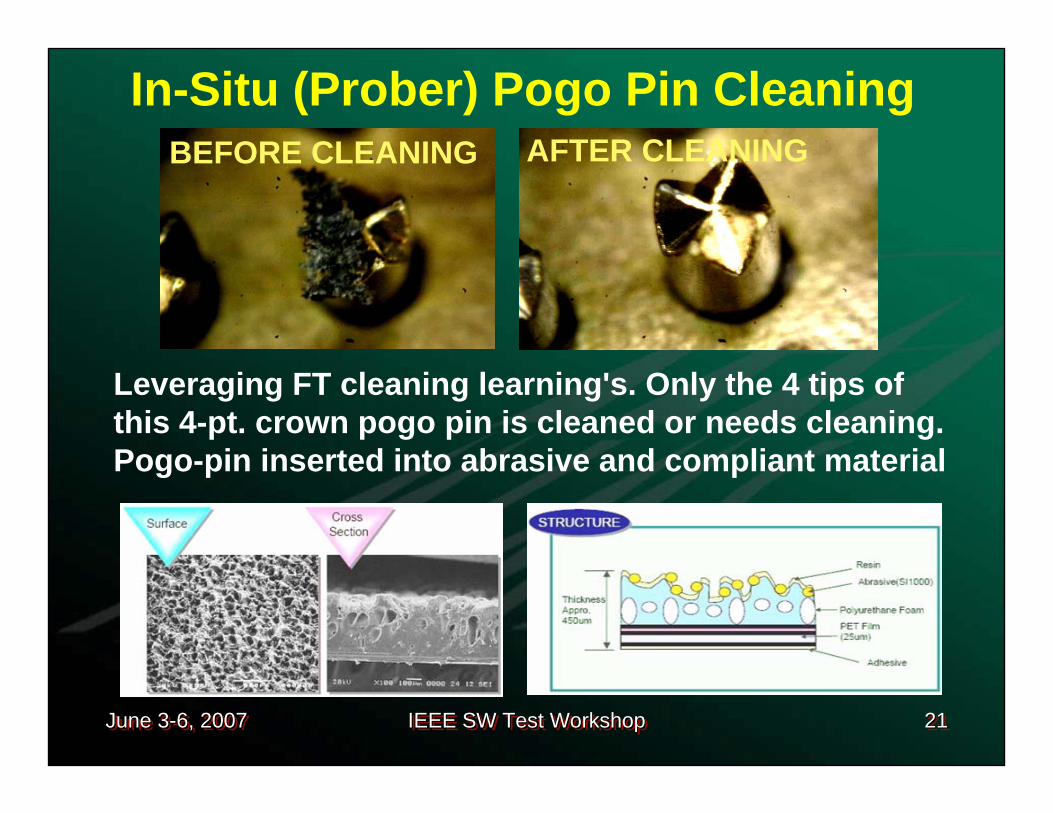
In-Situ (Prober) Pogo Pin CleaningBEFORE CLEANING AFTER CLEANING
Leveraging FT cleaning learning's. Only the 4 tips of this 4-pt. crown pogo pin is cleaned or needs cleaning. Pogo-pin inserted into abrasive and compliant material

June 3-6, 2007June 3June 3--6, 20076, 2007 IEEE SW Test WorkshopIEEE SW Test WorkshopIEEE SW Test Workshop 222222

June 3-6, 2007June 3June 3--6, 20076, 2007 IEEE SW Test WorkshopIEEE SW Test WorkshopIEEE SW Test Workshop 232323
Bump Surface Condition
Bump surface condition impacts pogo-pin ability to penetrate bump surface as well as, pogo-pins surface if not cleaned effectively for subsequent bump probing.
Carbon-Rich Areas

June 3-6, 2007June 3June 3--6, 20076, 2007 IEEE SW Test WorkshopIEEE SW Test WorkshopIEEE SW Test Workshop 242424
Pogo-Pin Condition
Cleaning media impacts Pogo-pin surface condition and subsequent electrical contact to bump, if cleaning settings not optimized.

June 3-6, 2007June 3June 3--6, 20076, 2007 IEEE SW Test WorkshopIEEE SW Test WorkshopIEEE SW Test Workshop 252525
500um 500um
Cleaning Stepping Distance
Increasing the stepping distances on cleaning media greatly improves cleaning efficiency. Although, at the expense of using more cleaning media.

June 3-6, 2007June 3June 3--6, 20076, 2007 IEEE SW Test WorkshopIEEE SW Test WorkshopIEEE SW Test Workshop 262626
Denotes “peace time”directly after online clean and before failures begin
Shows rise of minimum Creslevels after clean
UNIT_START_TIME
2
3
4
5
6
7
3/ 21/ 2007 9:37:5... 3/ 21/ 2007 10:... 3/ 21/ 2007 11:1... 3/ 21/ 2007 12:0... 3/ 21/ 2007 12:5... 3/ 21/ 2007 1:40:... 3/ 21/ 2007 2:30:... 3/ 21/ 2007 3:20:... 3/ 21/ 2007 4:10:00 PM
Online Clean
Failures BeginMax Cres(ohms)
TEST TIME (hrs)
Using CRes to Optimize Cleaning Parameters

June 3-6, 2007June 3June 3--6, 20076, 2007 IEEE SW Test WorkshopIEEE SW Test WorkshopIEEE SW Test Workshop 272727
Cleaning /Contamination
Issues
Gold Coating WearAffecting CRes
MechLifetime Plunger
100KTD200KTD
Current StartingStatus
30KTD
Key Milestones for WSP Probe Card Lifetime Optimization
TARGET

June 3-6, 2007June 3June 3--6, 20076, 2007 IEEE SW Test WorkshopIEEE SW Test WorkshopIEEE SW Test Workshop 282828
WSP PROBE CARD SUMMARY
High PriceF/D Limited RangeFew Qualified Suppliers Dense multi-site < x4
Electrical Properties >40 GHzPitch <0.3mmSmall scrub marks
MembraneProbe Beams
Current Pitch Limited to 0.4mmProber Integration, cleaning, etc.0.3mm PCB supplier baseLinear F / D
Low PriceElectrical Properties (5GHz)Small Marks on Sides of BumpMulti-site x8, x16
SocketPogo-Pins
Electrically LimitedInitial Price and Lead TimeBump-Top Damage/ ReflowProbe binding
Dense Multi-site x16F / D ProfileHi-Temp StabilityMany Qualified Suppliers
VPCBuckling Wires
Electrically LimitedArea Array limitedF / D Linear Bump-Top Damage/ Reflow
Low priceShort Lead-time for New Designs Repairable ContactsMany Qualified Suppliers
CantileverNeedles
CONsPROsTechnology

June 3-6, 2007June 3June 3--6, 20076, 2007 IEEE SW Test WorkshopIEEE SW Test WorkshopIEEE SW Test Workshop 292929
However, the challenge for a direct 0.3mm socket to PCB connection, is that the PCB technology is not converging to what a socket can be manufactured.
In other words, sockets can be manufactured <0.3mm pitch, but conventional PCB technology “cliff” is currently 0.4mm pitch
Probe Technology Probe Technology ““GateGate”” for for WLCSP EnablementWLCSP Enablement

June 3-6, 2007June 3June 3--6, 20076, 2007 IEEE SW Test WorkshopIEEE SW Test WorkshopIEEE SW Test Workshop 303030
• Optimize Prober/ Probe Card/ Wafer SettingsPlanarity vs Pogo-Pin Deflection Optimization Alignment Method / Algorithm
• Optimize Cleaning SettingsMedia / Tip DesignStepping
• Minimize Probe Card DeflectionTester PCSP DesignMechanical Stiffeners
• Printed Circuit Board Design/ Fab0.3mm pitchMulti-Site to x16
• Thermal CharacterizationCold Temp -40 CHigh Temp 129 C
Future Work

June 3-6, 2007June 3June 3--6, 20076, 2007 IEEE SW Test WorkshopIEEE SW Test WorkshopIEEE SW Test Workshop 313131
Acknowledgements
• Cody Gilleland• Doyce Ramey• Kelly Daughtry• Byron Gibbs