A Reliable Wafer-Level Chip Scale Package (WLCSP) Technology
7
Thank you! Thank you for downloading one of our whitepapers – we hope you enjoy it. Have questions? Need more information? Please don’t hesitate to contact us! We have plenty more where this came from. Sales Support Training Emag FEA CFD Ozen Engineering Inc. – ANSYS Channel Partner & Distributor 1210 East Arques Ave. #207, Sunnyvale, CA 94085 Telephone: (408) 732-4665 E-mail: [email protected] Web: www.ozeninc.com
-
Upload
ozen-engineering-inc -
Category
Documents
-
view
137 -
download
2
Transcript of A Reliable Wafer-Level Chip Scale Package (WLCSP) Technology

Thank you!
Thank you for downloading one of our whitepapers – we hope you enjoy it.
Have questions? Need more information?
Please don’t hesitate to contact us! We have plenty more where this came from.
Sales Support Training Emag FEA CFD
Ozen Engineering Inc. – ANSYS Channel Partner & Distributor
1210 East Arques Ave. #207, Sunnyvale, CA 94085
Telephone: (408) 732-4665
E-mail: [email protected]
Web: www.ozeninc.com
A RELIABLE WAFER-LEVEL CHIP SCALE PACKAGE (WLCSP)
TECHNOLOGY
Umesh Sharma, Ph.D., Philip Holland, and Harry Gee
California Micro Devices, Inc. Milpitas, CA
[email protected], [email protected], and [email protected] Metin Ozen, Ph.D., and Can Ozcan
Ozen Engineering, Inc. Sunnyvale, CA
[email protected], and [email protected]
ABSTRACT
In conventional WLCSP process, after defining the under bump metal (UBM) layer, a solder ball is dropped in the UBM opening. A subsequent thermal reflow cycle melts the solder ball and cools it in a well defined shape on top of the UBM layer. One draw back of this technology is the fracture or cracking of passivation film that may occur during the solder ball reflow process. The cracks in the passivation expose the underlying semiconductor devices to the ambient environment. Such cracks result in long term reliability problems or complete failure depending on the extent of the exposure to harmful ambient. In this paper, we systematically analyze the problem of passivation cracking and present a WLCSP process that is resistant to cracking during solder flow and subsequent multiple reflow steps. ANSYS thermo-mechanical finite element modeling software is used to model the WLCSP structure and process flow to evaluate stress and deformation at various points across the device structure. Contour plots clearly highlight the high stress regions and pinpoint the potential failure region. The use of ANSYS software in optimizing process parameters, and predicting reliability is presented. The experimental results confirm our simulation results and we conclude by presenting an optimized process that is resistant to passivation cracking and resulting failures. Keywords: WLCSP, passivation cracks, re-passivation, ANSYS, simulations INTRODUCTION AND PROBLEM DESCRIPTION
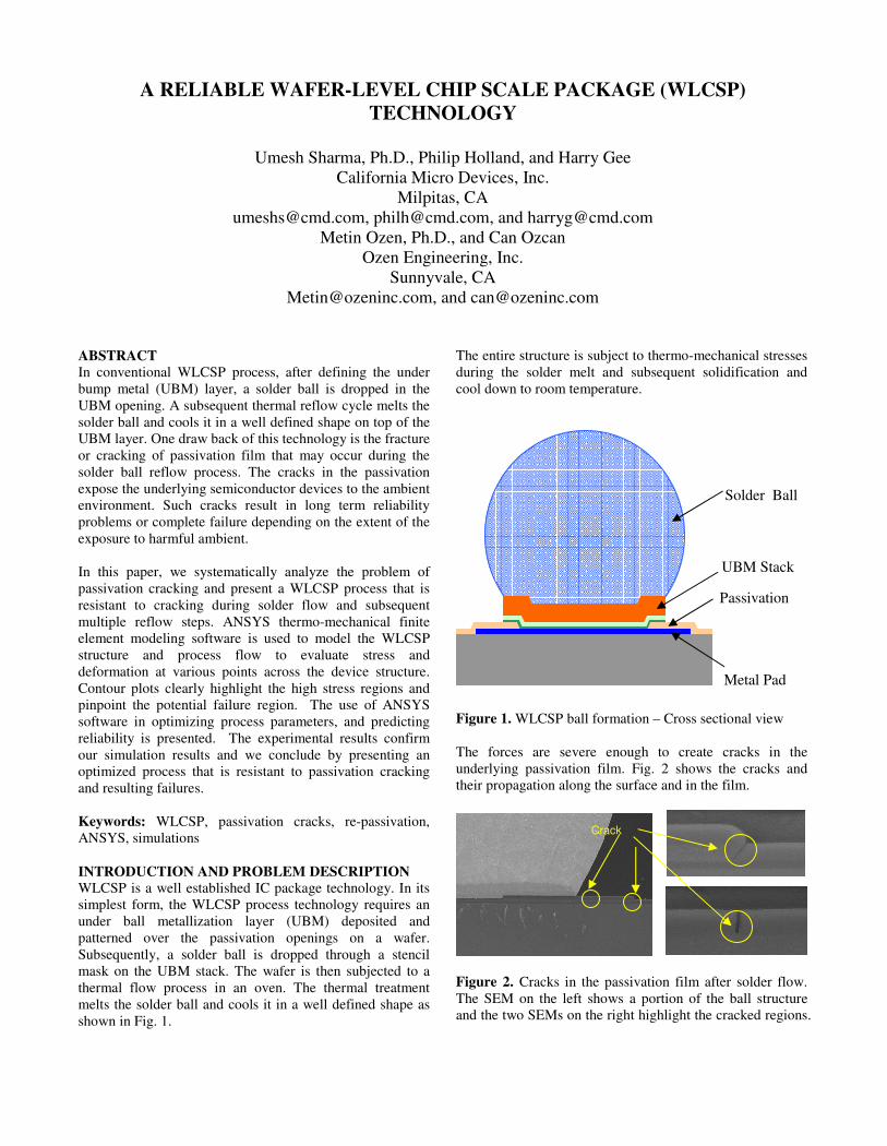
WLCSP is a well established IC package technology. In its simplest form, the WLCSP process technology requires an under ball metallization layer (UBM) deposited and patterned over the passivation openings on a wafer. Subsequently, a solder ball is dropped through a stencil mask on the UBM stack. The wafer is then subjected to a thermal flow process in an oven. The thermal treatment melts the solder ball and cools it in a well defined shape as shown in Fig. 1.
The entire structure is subject to thermo-mechanical stresses during the solder melt and subsequent solidification and cool down to room temperature.
Figure 1. WLCSP ball formation – Cross sectional view
The forces are severe enough to create cracks in the underlying passivation film. Fig. 2 shows the cracks and their propagation along the surface and in the film.
Figure 2. Cracks in the passivation film after solder flow. The SEM on the left shows a portion of the ball structure and the two SEMs on the right highlight the cracked regions.
Solder Ball
UBM Stack
Passivation
Metal Pad
Crack
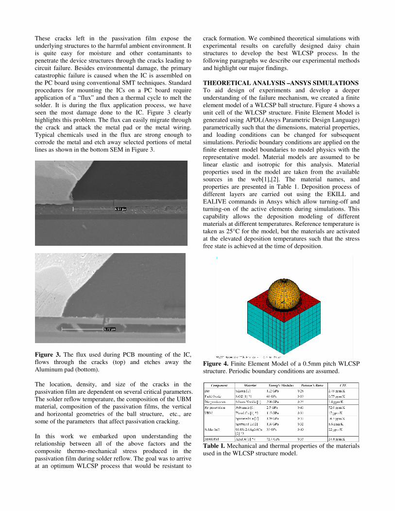
These cracks left in the passivation film expose the underlying structures to the harmful ambient environment. It is quite easy for moisture and other contaminants to penetrate the device structures through the cracks leading to circuit failure. Besides environmental damage, the primary catastrophic failure is caused when the IC is assembled on the PC board using conventional SMT techniques. Standard procedures for mounting the ICs on a PC board require application of a “flux” and then a thermal cycle to melt the solder. It is during the flux application process, we have seen the most damage done to the IC. Figure 3 clearly highlights this problem. The flux can easily migrate through the crack and attack the metal pad or the metal wiring. Typical chemicals used in the flux are strong enough to corrode the metal and etch away selected portions of metal lines as shown in the bottom SEM in Figure 3.
Figure 3. The flux used during PCB mounting of the IC, flows through the cracks (top) and etches away the Aluminum pad (bottom). The location, density, and size of the cracks in the passivation film are dependent on several critical parameters. The solder reflow temperature, the composition of the UBM material, composition of the passivation films, the vertical and horizontal geometries of the ball structure, etc., are some of the parameters that affect passivation cracking. In this work we embarked upon understanding the relationship between all of the above factors and the composite thermo-mechanical stress produced in the passivation film during solder reflow. The goal was to arrive at an optimum WLCSP process that would be resistant to
crack formation. We combined theoretical simulations with experimental results on carefully designed daisy chain structures to develop the best WLCSP process. In the following paragraphs we describe our experimental methods and highlight our major findings.
THEORETICAL ANALYSIS –ANSYS SIMULATIONS To aid design of experiments and develop a deeper understanding of the failure mechanism, we created a finite element model of a WLCSP ball structure. Figure 4 shows a unit cell of the WLCSP structure. Finite Element Model is generated using APDL(Ansys Parametric Design Language) parametrically such that the dimensions, material properties, and loading conditions can be changed for subsequent simulations. Periodic boundary conditions are applied on the finite element model boundaries to model physics with the representative model. Material models are assumed to be linear elastic and isotropic for this analysis. Material properties used in the model are taken from the available sources in the web[1],[2]. The material names, and properties are presented in Table 1. Deposition process of different layers are carried out using the EKILL and EALIVE commands in Ansys which allow turning-off and turning-on of the active elements during simulations. This capability allows the deposition modeling of different materials at different temperatures. Reference temperature is taken as 25°C for the model, but the materials are activated at the elevated deposition temperatures such that the stress free state is achieved at the time of deposition.
Figure 4. Finite Element Model of a 0.5mm pitch WLCSP structure. Periodic boundary conditions are assumed.
Table I. Mechanical and thermal properties of the materials used in the WLCSP structure model.
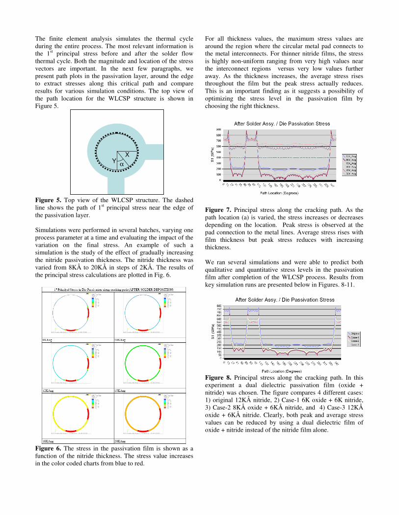
The finite element analysis simulates the thermal cycle during the entire process. The most relevant information is the 1st principal stress before and after the solder flow thermal cycle. Both the magnitude and location of the stress vectors are important. In the next few paragraphs, we present path plots in the passivation layer, around the edge to extract stresses along this critical path and compare results for various simulation conditions. The top view of the path location for the WLCSP structure is shown in Figure 5.
Figure 5. Top view of the WLCSP structure. The dashed line shows the path of 1st principal stress near the edge of the passivation layer. Simulations were performed in several batches, varying one process parameter at a time and evaluating the impact of the variation on the final stress. An example of such a simulation is the study of the effect of gradually increasing the nitride passivation thickness. The nitride thickness was varied from 8KÅ to 20KÅ in steps of 2KÅ. The results of the principal stress calculations are plotted in Fig. 6.
Figure 6. The stress in the passivation film is shown as a function of the nitride thickness. The stress value increases in the color coded charts from blue to red.
For all thickness values, the maximum stress values are around the region where the circular metal pad connects to the metal interconnects. For thinner nitride films, the stress is highly non-uniform ranging from very high values near the interconnect regions versus very low values further away. As the thickness increases, the average stress rises throughout the film but the peak stress actually reduces. This is an important finding as it suggests a possibility of optimizing the stress level in the passivation film by choosing the right thickness.
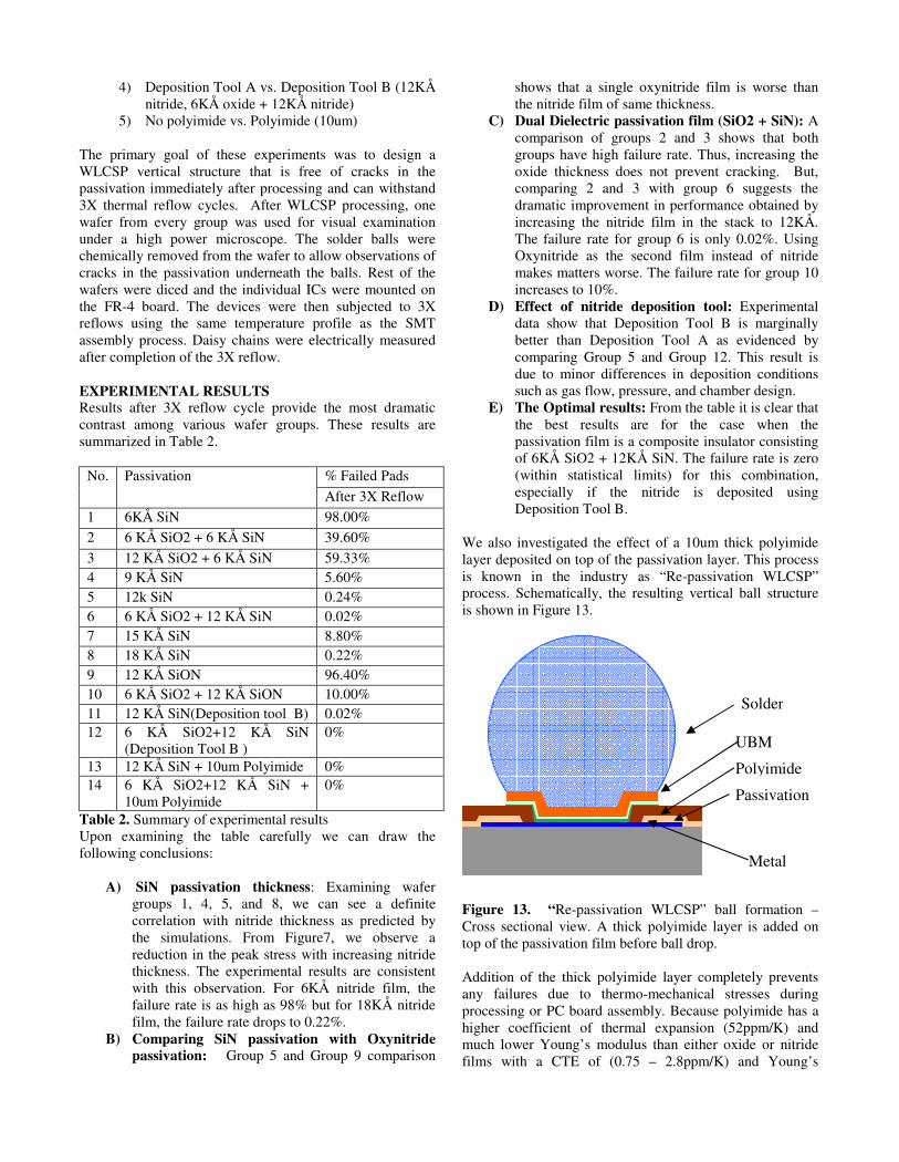
Figure 7. Principal stress along the cracking path. As the path location (a) is varied, the stress increases or decreases depending on the location. Peak stress is observed at the pad connection to the metal lines. Average stress rises with film thickness but peak stress reduces with increasing thickness. We ran several simulations and were able to predict both qualitative and quantitative stress levels in the passivation film after completion of the WLCSP process. Results from key simulation runs are presented below in Figures. 8-11.
Figure 8. Principal stress along the cracking path. In this experiment a dual dielectric passivation film (oxide + nitride) was chosen. The figure compares 4 different cases: 1) original 12KÅ nitride, 2) Case-1 6K oxide + 6K nitride, 3) Case-2 8KÅ oxide + 6KÅ nitride, and 4) Case-3 12KÅ oxide + 6KÅ nitride. Clearly, both peak and average stress values can be reduced by using a dual dielectric film of oxide + nitride instead of the nitride film alone.
α
X
Yα
X
Y
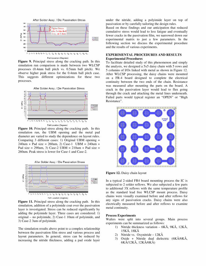
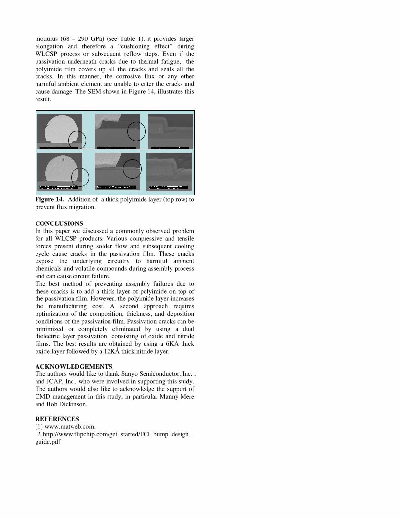
Figure 9. Principal stress along the cracking path. In this simulation run comparison is made between two WLCSP processes (0.4mm ball pitch vs. 0.5mm ball pitch). We observe higher peak stress for the 0.4mm ball pitch case. This suggests different optimizations for these two processes.
Figure 10. Principal stress along the cracking path. In this simulation run, the UBM opening and the metal pad diameter are varied to study the dependence on layout rules. Comparing 3 different cases: 1) Original UBM opening = 240um + Pad size = 260um, 2) Case-1 UBM = 240um + Pad size = 290um, 3) Case-2 UBM = 210um + Pad size = 260um. Peak stress is lower for Case-1 and Case-2.
Figure 11. Principal stress along the cracking path. In this simulation, addition of a polyimide coat over the passivation layer is investigated. Stress can be reduced significantly by adding the polyimide layer. Three cases are considered: 1) original – no polyimide, 2) Case-1 10um of polyimide, and 3) Case-2 3um of polyimide. The simulation results above point to a complex relationship between the passivation film stress and various process and layout parameters. In general, stress can be reduced by increasing the nitride thickness, adding a pad oxide layer
under the nitride, adding a polyimide layer on top of passivation or by carefully tailoring the design rules. Based on these findings and our anticipation that reduced cumulative stress would lead to less fatigue and eventually fewer cracks in the passivation film, we narrowed down our experimental matrix to just a few parameters. In the following section we discuss the experimental procedure and the results of various experiments. EXPERIMENTAL PROCEDURES AND RESULTS Experimental Procedures To facilitate detailed study of this phenomenon and simply the analysis, we designed a 5x5 daisy chain with 5 rows and 5 columns of I/Os linked with metal as shown in Figure 12. After WLCSP processing, the daisy chains were mounted on a FR-4 board designed to complete the electrical continuity between the two ends of the chain. Resistance was measured after mounting the parts on the board. A crack in the passivation layer would lead to flux going through the crack and attacking the metal lines underneath. Failed parts would typical register an “OPEN” or “High Resistance”.
Figure 12. Daisy chain layout In a typical 2-sided FR4 board mounting process the IC is subjected to 2 solder reflows. We also subjected a few parts to additional 3X reflows with the same temperature profile as the standard lead free WLCSP mount process. Daisy chains were visually examined before and after reflows for any signs of passivation cracks. Daisy chains were also electrically measured before and after reflows to examine metal continuity. Process Experiments Wafers were split into several groups. Main process experiments can be summarized as follows:
1) Nitride thickness variation – 6KÅ, 9KÅ, 12KÅ, 15KÅ, 18KÅ
2) Nitride vs. Oxynitride – 12KÅ 3) Oxide + Nitride dual dielectric (6KÅ/6KÅ,
6KÅ/12KÅ, 12KÅ/6KÅ)
4) Deposition Tool A vs. Deposition Tool B (12KÅ nitride, 6KÅ oxide + 12KÅ nitride)
5) No polyimide vs. Polyimide (10um) The primary goal of these experiments was to design a WLCSP vertical structure that is free of cracks in the passivation immediately after processing and can withstand 3X thermal reflow cycles. After WLCSP processing, one wafer from every group was used for visual examination under a high power microscope. The solder balls were chemically removed from the wafer to allow observations of cracks in the passivation underneath the balls. Rest of the wafers were diced and the individual ICs were mounted on the FR-4 board. The devices were then subjected to 3X reflows using the same temperature profile as the SMT assembly process. Daisy chains were electrically measured after completion of the 3X reflow.
EXPERIMENTAL RESULTS Results after 3X reflow cycle provide the most dramatic contrast among various wafer groups. These results are summarized in Table 2.
% Failed Pads No. Passivation After 3X Reflow
1 6KÅ SiN 98.00% 2 6 KÅ SiO2 + 6 KÅ SiN 39.60% 3 12 KÅ SiO2 + 6 KÅ SiN 59.33% 4 9 KÅ SiN 5.60% 5 12k SiN 0.24% 6 6 KÅ SiO2 + 12 KÅ SiN 0.02% 7 15 KÅ SiN 8.80% 8 18 KÅ SiN 0.22% 9 12 KÅ SiON 96.40% 10 6 KÅ SiO2 + 12 KÅ SiON 10.00% 11 12 KÅ SiN(Deposition tool B) 0.02% 12 6 KÅ SiO2+12 KÅ SiN
(Deposition Tool B ) 0%
13 12 KÅ SiN + 10um Polyimide 0% 14 6 KÅ SiO2+12 KÅ SiN +
10um Polyimide 0%
Table 2. Summary of experimental results Upon examining the table carefully we can draw the following conclusions:
A) SiN passivation thickness: Examining wafer groups 1, 4, 5, and 8, we can see a definite correlation with nitride thickness as predicted by the simulations. From Figure7, we observe a reduction in the peak stress with increasing nitride thickness. The experimental results are consistent with this observation. For 6KÅ nitride film, the failure rate is as high as 98% but for 18KÅ nitride film, the failure rate drops to 0.22%.
B) Comparing SiN passivation with Oxynitride
passivation: Group 5 and Group 9 comparison
shows that a single oxynitride film is worse than the nitride film of same thickness.
C) Dual Dielectric passivation film (SiO2 + SiN): A comparison of groups 2 and 3 shows that both groups have high failure rate. Thus, increasing the oxide thickness does not prevent cracking. But, comparing 2 and 3 with group 6 suggests the dramatic improvement in performance obtained by increasing the nitride film in the stack to 12KÅ. The failure rate for group 6 is only 0.02%. Using Oxynitride as the second film instead of nitride makes matters worse. The failure rate for group 10 increases to 10%.
D) Effect of nitride deposition tool: Experimental data show that Deposition Tool B is marginally better than Deposition Tool A as evidenced by comparing Group 5 and Group 12. This result is due to minor differences in deposition conditions such as gas flow, pressure, and chamber design.
E) The Optimal results: From the table it is clear that the best results are for the case when the passivation film is a composite insulator consisting of 6KÅ SiO2 + 12KÅ SiN. The failure rate is zero (within statistical limits) for this combination, especially if the nitride is deposited using Deposition Tool B.
We also investigated the effect of a 10um thick polyimide layer deposited on top of the passivation layer. This process is known in the industry as “Re-passivation WLCSP” process. Schematically, the resulting vertical ball structure is shown in Figure 13.
Figure 13. “Re-passivation WLCSP” ball formation – Cross sectional view. A thick polyimide layer is added on top of the passivation film before ball drop. Addition of the thick polyimide layer completely prevents any failures due to thermo-mechanical stresses during processing or PC board assembly. Because polyimide has a higher coefficient of thermal expansion (52ppm/K) and much lower Young’s modulus than either oxide or nitride films with a CTE of (0.75 – 2.8ppm/K) and Young’s
b
Solder
UBM
Passivation
Metal
Polyimide
modulus (68 – 290 GPa) (see Table 1), it provides larger elongation and therefore a “cushioning effect” during WLCSP process or subsequent reflow steps. Even if the passivation underneath cracks due to thermal fatigue, the polyimide film covers up all the cracks and seals all the cracks. In this manner, the corrosive flux or any other harmful ambient element are unable to enter the cracks and cause damage. The SEM shown in Figure 14, illustrates this result.
Figure 14. Addition of a thick polyimide layer (top row) to prevent flux migration. CONCLUSIONS
In this paper we discussed a commonly observed problem for all WLCSP products. Various compressive and tensile forces present during solder flow and subsequent cooling cycle cause cracks in the passivation film. These cracks expose the underlying circuitry to harmful ambient chemicals and volatile compounds during assembly process and can cause circuit failure. The best method of preventing assembly failures due to these cracks is to add a thick layer of polyimide on top of the passivation film. However, the polyimide layer increases the manufacturing cost. A second approach requires optimization of the composition, thickness, and deposition conditions of the passivation film. Passivation cracks can be minimized or completely eliminated by using a dual dielectric layer passivation consisting of oxide and nitride films. The best results are obtained by using a 6KÅ thick oxide layer followed by a 12KÅ thick nitride layer. ACKNOWLEDGEMENTS
The authors would like to thank Sanyo Semiconductor, Inc. , and JCAP, Inc., who were involved in supporting this study. The authors would also like to acknowledge the support of CMD management in this study, in particular Manny Mere and Bob Dickinson. REFERENCES
[1] www.matweb.com. [2]http://www.flipchip.com/get_started/FCI_bump_design_guide.pdf