
10 Steps to Increase HDI Membership - South Florida HDI Local Chapter
Upload
duongxuyenCategory
view
215download
0
Highly Reliable HDI
Blind & Buried Vias
Via-In-Pad & Laser Microvias
Basic Design Rules for Reliable PCBs
Donald A. Carron, C.I.D.
Director of Technology

The Goal of This Presentation
To provide modern PCB designers with a review of robust
rules and methods that will allow them to design a highly
reliable printed circuit board with the lowest cost, most
commonly used features, and least number of
manufacturing issues (that may result in a no-bid,
engineering questions, placing the job on hold, or
negatively impact the final yield).

During the writing of his book A Brief History Of Time the
publisher told Stephen Hawking that if he included even one
equation in the book it would effectively cut his prospective
readership in half!
So in that spirit I will leave the equations to others that wish
to use them in their own presentations.
I promise to keep it simple and to the point.
The Contents of This Presentation
There are specific design rules available from the individual
packaging suppliers (ex: Xilinx, Altera, Texas Instruments,
Motorola, etc.) for device footprint layout metrics. We will not
provide pad diameters, trace widths, spacing, etc. for each ball
land pitch (0.5mm, 0.4mm, 0.3mm, etc.) as they are readily
available from the manufacturers online.
Here we only wish to provide the minimums that if adhered to
will provide the designer with a highly reliable physical PCB.

Rather than provide specific routing examples such as those below I would
prefer to focus on design minimums as these boundaries are routinely pushed
or broken in modern PCB design…
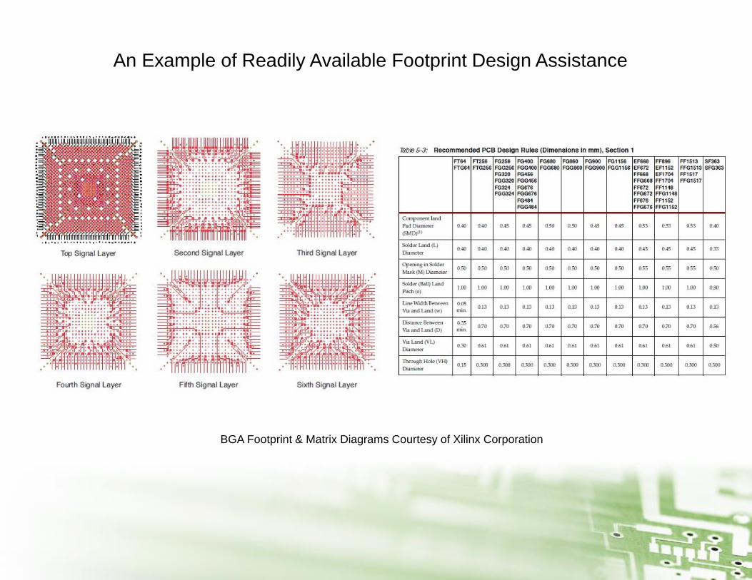
BGA Footprint & Matrix Diagrams Courtesy of Xilinx Corporation
An Example of Readily Available Footprint Design Assistance

A Paradigm Shift in Technology
Today we are faced with a rapid reduction of PCB feature
sizes due to the need for reduced form factor with fine pitch
BGAs and small surface mount devices, and reduction or
elimination of legacy components (replaced with ever
smaller and denser packages).
Add to this an increasing number of designers entering the
workforce without experience in required design
technologies (blind & buried vias, sequential lamination, via-
in-pad, laser microvias, etc.).
This combination is a growing concern in the industry…

But First:
Some simple PCB review. Let’s get back
to basics to lend perspective to today’s
presentation…

In their most basic form, via holes are used to connect traces from
one board layer to another. Generally it enables a direction
change (in the X or Y axis) in order to bypass device footprints
and route signals from one end of the PCB to the other.

In this photo of a simple 1980’s PCB, the via holes are circled
in red in this photo to distinguish them from the soldered
component holes, which were mainly for DIPs.
There were very few hole sizes required—plated component
and via holes, and non-plated tooling hole diameters.
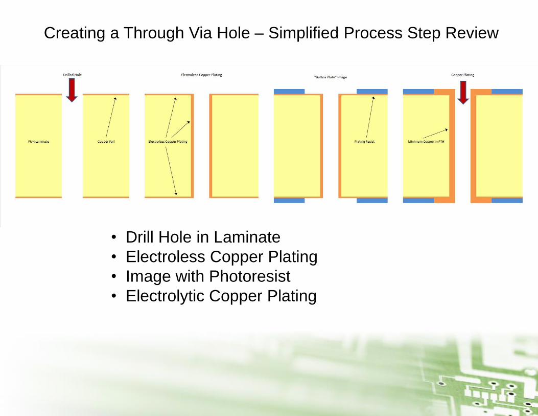
Creating a Through Via Hole – Simplified Process Step Review
• Drill Hole in Laminate
• Electroless Copper Plating
• Image with Photoresist
• Electrolytic Copper Plating

Aspect Ratio of a Drilled Via Hole: Depth to Diameter (Example: 10:1 A/R)

Aspect Ratio – Mechanically Drilled Via vs. Laser Microvia

Plated Through Hole - Microsection
Copper Plating at Knee
Copper Plating in Center
Copper plated component and via
holes must be plated evenly from the
“knee” to the center of the PTH. The
outer areas of the hole generally plate
faster which creates a “dog bone”
plating profile in the PTH.
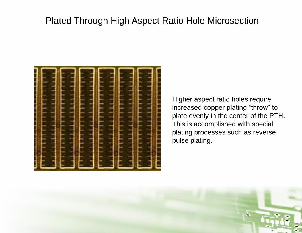
Plated Through High Aspect Ratio Hole Microsection
Higher aspect ratio holes require
increased copper plating “throw” to
plate evenly in the center of the PTH.
This is accomplished with special
plating processes such as reverse
pulse plating.
Via-In-Pad
Definition:
A via interconnect hole that resides in a solderable pad, where the
requirements are for a flat, planar surface that does not contribute negatively
to the placement or orientation of the soldered component.
Common Method of Creating Via-In-Pad:
1) Using mechanical drills, the via spans one or several dielectrics
and conductive layers, and is filled (post-plating) with a conductive or non-
conductive epoxy material that is void-free and facilitates a planar surface to
create the surface pad that a device will be soldered to.
2) Using laser ablation, the microvia spans a single dielectric and
connects the surface layer to the next layer down in the stackup (except
variable-depth microvias). The subsequent microvia is fully copper plated
and planarized to create a flat surface pad that a device will be soldered to.

Via Illustration – PTH, Mechanical VIP, Microvia

Next:
We will define some minimum design rules
that should be considered in order to build
a reliable physical printed circuit board.
Note that these rules are broken every
day, and in some cases for good reasons.
But they are proven to assure reliability.

Designed Annular Ring for Mechanically Drilled PTHs.
IPC Class 2 Commercial & Class 3 High Reliability Minimums

Epoxy Filled Mechanically Drilled VIP
Minimums & Maximums for >/= 97% Fill Requirements
Minimum:
The minimum finished hole size (FHS) after plating is 0.008”
Maximum:
The maximum finished hole size (FHS) after plating is 0.018”
Reason:
FHS smaller than 0.008” are too small to reliably guarantee a
complete epoxy fill using a single pass process (due to PTH plating profiles,
hole wall irregularities, etc. present in 0.006” or smaller drilled vias).
FHS larger than 0.018” are typically too large to contain the epoxy
fill material (without running out of the hole due to viscosity) prior to thermal
curing. Aspect ratio plays a large part in this.
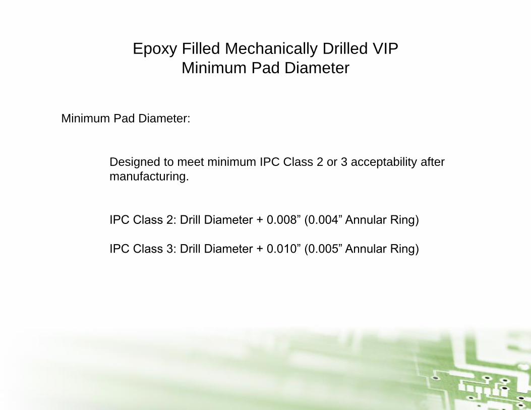
Epoxy Filled Mechanically Drilled VIP
Minimum Pad Diameter
Minimum Pad Diameter:
Designed to meet minimum IPC Class 2 or 3 acceptability after
manufacturing.
IPC Class 2: Drill Diameter + 0.008” (0.004” Annular Ring)
IPC Class 3: Drill Diameter + 0.010” (0.005” Annular Ring)

Laser Drilled VIP
Minimum Pad Diameter
Minimum Pad Diameter:
Designed to meet minimum IPC Class 2 or 3 acceptability after
manufacturing.
IPC Class 2: Drill Diameter + 0.004” (0.002” Annular Ring)
IPC Class 3: Drill Diameter + 0.004” (0.002” Annular Ring)
Why is this?
The laser hole pattern registers to the sub-layer and scales accurately to
match it in X/Y, so less A/R is required. Also, because laser microvias are
fully copper filled (plated completely from bottom to top and planarized flat),
there is no visible annular ring on the outer layer of the final product.

Mechanically Drilled Via Hole Epoxy Materials Example: Two of Each Type Commonly Used
Conductive Epoxies (ex: Silver Coated Copper Particulates):
• DuPont CB-100
• Tatsuta AE3030
Non-Conductive Epoxies:
• San-Ei Kagaku PHP-900 IR10F
• Peters PP2795
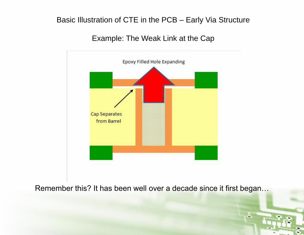
Basic Illustration of CTE in the PCB – Early Via Structure
Example: The Weak Link at the Cap
Remember this? It has been well over a decade since it first began…

Pre IPC-6012B Filled Via Hole Cross-Section

Post IPC-6012B Filled Via Hole Cross-Section

IPC-6012B Via-In-Pad Wrap Requirements
IPC-6012 Class 2:
A minimum of 0.0002” plated copper is required at the knee of the
hole extending a minimum of 0.001” on to the surface (within the associated
pad).
IPC-6012 Class 3:
A minimum of 0.0005” plated copper is required at the knee of the
hole extending a minimum of 0.001” on to the surface (within the associated
pad).

PTH Wrap Process – Step 1
First step of the sequence – the laminated board is drilled with the bit
diameters that will produce the correct finished hole size after the
plating operations.
Sequence Diagrams Show PCB in PTH Microsection Profile Perpendicular to Surface

PTH Wrap Process – Step 2
Second step of the sequence – the drilled board is panel plated to
produce the minimum plated wrap thickness:
IPC-6012 Class 2 = 0.0002” minimum
IPC-6012 Class 3 = 0.0005” minimum
Panel Plated Wrap

PTH Wrap Process – Step 3
Third step of the sequence – the board is imaged and developed with a
“button” that will produce a plated hole pad around the via hole.

PTH Wrap Process – Step 4
Fourth step of the sequence – the hole is pattern plated to produce the
minimum thickness copper plating in the hole per IPC-6012 Class 2 or
Class 3. The photo resist is then stripped leaving the plated “button”
pad surrounding the plated through hole.
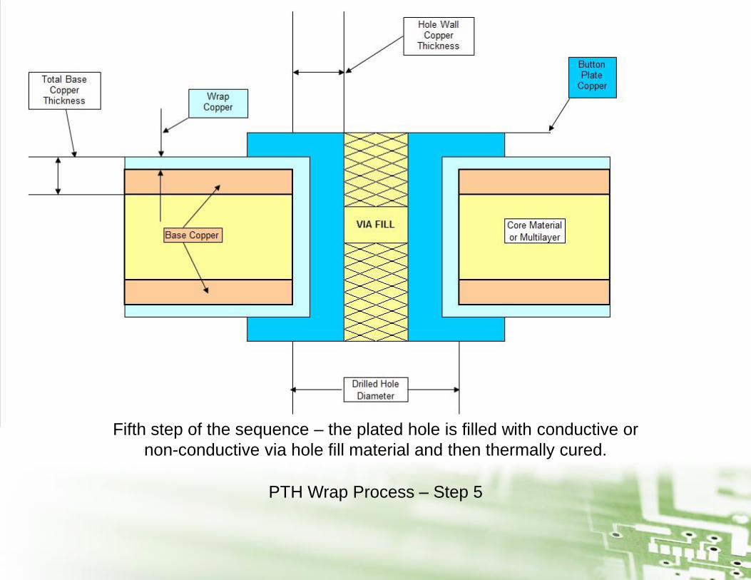
PTH Wrap Process – Step 5
Fifth step of the sequence – the plated hole is filled with conductive or
non-conductive via hole fill material and then thermally cured.

PTH Wrap Process – Step 6
Sixth step of the sequence – the excess via fill material along with the
plated “button” is planarized back to the wrap copper surface.

PTH Wrap Process – Step 7
Seventh step of the sequence (combined processes) – the panel has
been processed through electroless copper (to metallize the via fill
material), a subsequent flash plate to “cap” the hole, and finally the
pattern plate image and plating operation to produce the final features.
This simplified diagram shows the circuit image prior to final etch.

PTH Wrap Process – Step 8
Eighth step of the sequence – the board is etched to produce the final
pattern. Note the cross-section of the circuit and pad sections: The final
thickness is based on the minimum wrap thickness plus minimum hole
plating thickness to meet IPC-6012 Class 2 or Class 3. This combined
copper thickness may limit the finished line width due to etch limitations.

The required minimum copper thickness specifications of both the IPC-
6012 wrap plating and final plated through hole thickness becomes the
limiting factor for trace and space widths. For example, if the
specification is IPC-6012 Class 3 then the minimum copper thickness is
determined by the following:
Minimum Class 3 wrap thickness: 0.0005”
Minimum Class 3 plated through hole thickness: 0.001”
Add to that:
Base copper foil thickness: 3/8 ounce aka 12 micron (0.000525”) or 0.5
ounce (0.0007”)
Also consider slightly more thickness (0.0002” typ.) added at each
plating operation to assure that minimums are met.
Combine all of the plating steps with the base copper thickness and the
sum will be the amount of copper that will determine the MINIMUM
trace width and spacing that can be achieved.
How Wrap Requirements Determine Trace Width / Space
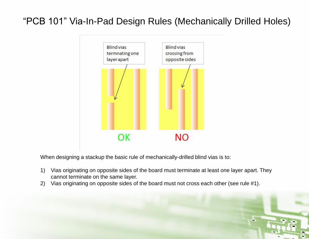
“PCB 101” Via-In-Pad Design Rules (Mechanically Drilled Holes)
When designing a stackup the basic rule of mechanically-drilled blind vias is to:
1) Vias originating on opposite sides of the board must terminate at least one layer apart. They
cannot terminate on the same layer.
2) Vias originating on opposite sides of the board must not cross each other (see rule #1).

Next: Microvias – Laser Formed Plated Via Interconnects
Image Courtesy of Polar Instruments

Microvias
“With the introduction of the Ball Grid Array
(BGA), board feature dimensions began dropping
from fractions of an inch to thousandths of an inch
until it became clear that the traditional
manufacturing technologies had reached a point
where they could no longer do the same things in
the same ways, only smaller. A new revolution
was upon the industry, one dubbed the Density
Revolution, and it continues today. It has officially
become the High-Density Interconnect (HDI)
Revolution.” The HDI Handbook

IPC-2226 1.5.2 HDI Types (I, II, & III of VI)
• TYPE I – (1 + n + 1) – Laser Microvias on Both
Sides of the Board.
• TYPE II – (1 + n + 1) – Laser Microvias on Both
Sides of the Board, with Buried Vias in the Core.
• TYPE III – (2 + n + 2) – Laser Microvias on Both
Sides of the Board—may Have Buried Vias in the
Core.
Microvias

Microvias – Type I

Microvias – Type II

Microvias – Type III

Microvias – Type III Stacked


Microvias – Aspect Ratio
Aspect Ratio is very important in microvia formation. The current
standard remains a most manufacturable 0.5:1 aspect ratio.

Microvias – Stacked Microvias
With the advent of fine-pitch BGAs with many more rows of interconnects it is necessary
to stack microvias to route surface signals to multiple layers below. Due to the tight
spacing a single track between pads may not be feasible (due to greatly decreased line
widths) so the ability to drop down another layer to fan out the signal is mandatory.
The flip side of this is the increased CTE mismatch between the solid copper microvia
structure and the surrounding laminate. Laminate/copper stress cracks are more likely in
stacks exceeding a 3 high structure (with typical PCB microvia diameters). Note that the
CSP world has been doing this for many years successfully stacking 5 high +, but at
much smaller diameters and dielectrics on different substrates.

CTE & Stacked Via Structures
CTE plays a key role in the reliability of filled vias, and an even more critical
factor when via structures are directly stacked.
In the microsection photo below, the CTE mismatch between fill, plating and
laminate become amplified by the increased Z-axis of the stacked microvia
structures directly on top of the buried/filled via.
This is an older industry photo showing epoxy filled microvias but still serves
to illustrate stacked microvias over filled buried vias.

CTE & Stacked Via Structures
When stacked microvia on buried/filled via structures are required, it is a
better practice to offset the microvia structure from the buried/filled via. This
allows both structures to expand and contract, but lessen the probability of a
stress crack propagating within the padstack intersections.
Okay, so where is this all going?
The packages are getting smaller every day,
which necessitates smaller pad diameters
resulting in two distinct issues:
1) Pads </= 0.006” have reduced adhesion.
2) Smaller microvias require thinner dielectrics.

Remember RCC (RCF)?
It was a boon for cell phone designs and a clean
laser-drilled microvia was easy with a thin
dielectric that did not have e-glass. But this lack
of e-glass created its own set of issues,
particularly X/Y dimensional stability.

So Welcome to the Next Generation of
Microvia Dielectrics!
Integral Technologies Zeta materials (particularly
ZetaLam HDI dielectric) provides better
adhesion of small diameter pads along with a
thin non e-glass dielectric layer for excellent
hole formation.
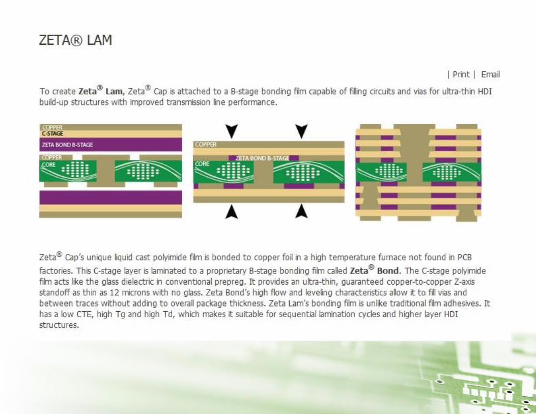

Okay, so what is possible now?
Microvias of 0.002” diameter with an aspect ratio of
much less than 1:1 are possible with ZetaLam.
1) Pads of 0.006” diameter have adhesion and
avoid “pad cratering” at assembly.
2) Smaller microvia aspect ratio is possible due to
the thin dielectrics.
High Reliability is Maintained!

Follow-Up Q&A


Advanced Circuits Contact Information
Sales:
Crystal Hardy
Cell: 619-889-7672
Email: [email protected]
Technology / Engineering:
Don Carron, C.I.D.
Cell: (480) 682-8126
Email: [email protected]


![INHALT - CONTENTS - MATIÈRE · RHZ(DW10ATED); (66kW-120kW) 1.6 HDi; 1.6 HDi 110; 1.6 HDi 110 FAP; 1.6 HDi 110 FAP [04]; 1.6 HDi 110FAP; 1.6 HDi 90; 1.6 HDi 90 [04]; 2.0 HDi; 2.0](https://static.fdocuments.in/doc/165x107/605cc6e9948bf00b8613e09d/inhalt-contents-matire-rhzdw10ated-66kw-120kw-16-hdi-16-hdi-110-16.jpg)
