HIGH SPEED LASER ABLATION OF MICROVIA … · HIGH SPEED LASER ABLATION OF MICROVIA HOLES ... Class...
12
1 HIGH SPEED LASER ABLATION OF MICROVIA HOLES IN NONWOVEN ARAMID REINFORCED PRINTED WIR- ING BOARDS TO REDUCE COST by Michael Weinhold Product Applications Manager DuPont Electronics, Geneva, Switzerland and David J. Powell, Senior Development Engineer DuPont Advanced Fiber Systems, Wilmington, DE, USA Biographies Michael Weinhold was born in the Federal Republic of Germany, where he obtained qualifications in Business Economics and Engineering. Mr. Weinhold has worked in the printed circuit industry since 1964. He is a member of the Board of Directors of the European Institute of Printed Circuits (EIPC). He represents Swit- zerland at the IEC -TC 52 and TC 91 committees, writing standards for the PCB fabrication and assembly industry. He is a Co-Founder of the ICDA (the Interna- tional Circuit Designers Association). Since joining DuPont in 1970, Mr. Weinhold has held various technical and product marketing assignments with the “RISTON®” Products Division. He is currently Product Application Manager, where his work relates to the latest developments in new Thermount® 100% aramid laminate rein- forcements, PWB image transfer technologies, as well as in SMD fine pitch, BGA and Flip Chip component soldering technologies. David J. Powell is a Senior Development Engineer with the DuPont Com- pany, Wilmington, DE. Since obtaining a B.S. degree in Chemistry from Bates Col- lege, he has accumulated fifteen years of manufacturing, engineering, and develop- ment experience in the printed wiring board industry. He is presently working on the development of new nonwoven aramid reinforcements for laminates and prepregs. Mr. Powell is a member of the North East Circuits Association, ISHM, and the IPC. Michael Weinhold David J. Powell
Transcript of HIGH SPEED LASER ABLATION OF MICROVIA … · HIGH SPEED LASER ABLATION OF MICROVIA HOLES ... Class...

1
HIGH SPEED LASER ABLATION OF MICROVIA HOLESIN NONWOVEN ARAMID REINFORCED PRINTED WIR-ING BOARDS TO REDUCE COSTby
Michael WeinholdProduct Applications ManagerDuPont Electronics, Geneva, Switzerlandand
David J. Powell,Senior Development EngineerDuPont Advanced Fiber Systems, Wilmington, DE, USA
BiographiesMichael Weinhold was born in the Federal Republic of Germany, where he
obtained qualifications in Business Economics and Engineering. Mr. Weinhold hasworked in the printed circuit industry since 1964. He is a member of the Board ofDirectors of the European Institute of Printed Circuits (EIPC). He represents Swit-zerland at the IEC -TC 52 and TC 91 committees, writing standards for the PCBfabrication and assembly industry. He is a Co-Founder of the ICDA (the Interna-tional Circuit Designers Association). Since joining DuPont in 1970, Mr. Weinholdhas held various technical and product marketing assignments with the “RISTON®”Products Division. He is currently Product Application Manager, where his workrelates to the latest developments in new Thermount® 100% aramid laminate rein-forcements, PWB image transfer technologies, as well as in SMD fine pitch, BGAand Flip Chip component soldering technologies.
David J. Powell is a Senior Development Engineer with the DuPont Com-pany, Wilmington, DE. Since obtaining a B.S. degree in Chemistry from Bates Col-lege, he has accumulated fifteen years of manufacturing, engineering, and develop-ment experience in the printed wiring board industry. He is presently working on thedevelopment of new nonwoven aramid reinforcements for laminates and prepregs.Mr. Powell is a member of the North East Circuits Association, ISHM, and the IPC.
Michael Weinhold
David J. Powell

2
IntroductionTo interconnect chips with finer pitch sizes and
higher I/O counts, designers of printed wiring boards havegradually selected finer lines, smaller holes and pads, andadditional layers to wire the required number of compo-nents into a given wiring area. Improving line resolutionand reducing drilled hole size has yielded the best economytowards achieving higher interconnect density withoutescalating costs. The PWB fabrication industry has de-veloped equipment and processes which produce 0.005”(125 µm) lines/spaces with 0.012” (300 µm) drilled holesin 4-10 layer PWBs at yields in excess of 90 per cent.Adding wiring layers contributes significantly tomultilayer printed wiring board cost and is chosen as alast resort.
Lowering costs and increasing wiringdensity
There is a continuing drive to lower PWB costs,while interconnecting chips with even higher I/Os (>400leads), by both reducing layer count and the size of the
Blind microvia holes with multiple lines around pads
Increased Routing Density using Micro-Via-Hole Technology
Through-hole technology
Standard technologyNew technology
Figure 1. Comparison of blind micro-via holeinterconnect scheme vs. through-via hole.
HIGH SPEED LASER ABLATION OF MICROVIA HOLES INNONWOVEN ARAMID REINFORCED PRINTED WIRING BOARDS
TO REDUCE COSTby
Michael WeinholdProduct Applications Manager
DuPont Electronics,, Geneva, Switzerlandand
David J. Powell,Senior Development Engineer
DuPont Advanced Fiber Systems, Wilmington, DE, USA
AbstractEmerging ‘chip-size’ IC packages, and bare flip-chips, require new substrate properties if high lead count
chips are to be reliably interconnected on printed wiring boards and multichip modules at low cost. Blind viaholes have been shown to significantly increase interconnect density without adding layers which contribute tohigh cost. Until recently, the use of blind vias has been limited to high-end applications since standard fabrica-tion methods, either sequential lamination or controlled depth drilling, are too slow and expensive for most highvolume commercial applications. To maintain a low layer count while inter-connecting higher I/O packages,commercial and consumer electronics requires a substrate technology which supports high speed, micro-viahole formation.
This paper describes a process for fabricating high speed micro-vias in dimensionally stable nonwovenaramid reinforced laminates using laser ablation technology. Laser equipment capable of producing over 100blind micro-via holes per second will be discussed. The process steps of hole cleaning and plating will bereviewed, showing how existing PWB manufacturing technologies can be used. This process will be comparedwith other methods of generating small holes and blind vias in printed wiring boards. In addition, requirementsfor flip-chip and chip-size packages, including a coefficient of thermal expansion of <10 ppm/˚C and thinlaminate dimensional stability of <0.03%, will be explained.

3
These are laser ablation, plasma etching, and photo-de-fined vias3. These technologies can also be combined withconventional drilling and traditional substrates to yieldthe most cost-effective solution, as demonstrated in PWBsmanufactured by Schoeller Elektronik (Figure 2) andMommers Print Service (Figure 3).
While each small hole formation technology ispromising, laser ablation is the easiest process to imple-ment in conventional PWB fabrication processes whileminimizing investment. Since lasers produce a collimatedetch source, hole geometry can be controlled and the re-sulting hole quality is excellent. Laser drilling equipmentis now commercially available in the price range of 250-375 thousand dollars, producing 10-150 holes per sec-ond. When, in the PWB fabrication process, this equip-ment is positioned after the conventional mechanical drill-ing operation for tooling holes and large connector holes,ultra small micro-vias can be produced at low cost with-out disrupting the process flow. Standard hole cleaning,metalization and finishing processes follow laser abla-tion, yielding a high density PWB with fewer intercon-nect layers.
On the other hand, the photo-imageable dielec-tric materials require major investment in coating lines,
Class 1000 clean rooms and changes in plating proc-esses. The thin, non-reinforced dielectric between lay-ers forces the fabricator to produce ultra fine lines(≤0.003” (75 µm)) for matched impedance which im-pacts on product yields. Sequential build-up of layersusing photo-imageable resists magnifies the yield losson subsequent operations. This technology has alsobeen found to introduce planarity problems for surfacemount components.
Plasma etching of micro-vias offers many of theadvantages of laser ablation. However, since plasmahas an isotropic etch behaviour, it is more difficult toform blind micro-vias without introducing undercut andpotential plating problems. These issues have been over-
interconnect holes. The latest ASICs, packaged in ceramicand plastic BGAs, require additional PWB layers to wirearea array pad configurations using conventional plated-through-hole technology1. Furthermore, ‘Chip size pack-aging driven by small size, lower profile and weight, andhigher speed’2 has placed even greater demand on PWB
routing density.
The most efficient method of reducing the volumeof space consumed by the layer-to-layer interconnects is ablind via hole (Figure 1). Blind via holes, if small enough,can be placed in the component pad, saving considerablerouting area around the component for high density wir-ing. To date, blind vias have been manufactured using tech-niques which produce either large holes or with fabrica-tion techniques, such as sequential lamination and control-led depth drilling, which are too costly for most commer-cial applications.
Small hole generationSeveral technologies are under development to meet
the electronic industry’s need for small blind via intercon-nects. Three techniques offer the greatest opportunity todeliver small holes at a low cost in large scale production.
Figure 2. Laser ablated blind via holes and plasma ablatedburied via holes in non-woven aramid.
(Courtesy of Schoeller Elektronik)
Thermount® Aramid Hybrid Multilayer Outerlayers in Aramid and innerlayer in FR4 construction
FR 4 core
2 layers of Thermount nonwoven Aramid
2 layers of Thermount nonwoven Aramid
Figure 3. Laser ablated blind via holes and mechanicallydrilled holes in non-woven aramid with a FR-4 core.(Courtesy of Mommers Print Service, Echt, Holland)
SMT and BGA with Microvias in Pads
Present Technology
Present Technology
NewTechnology
NewTechnology
QFP Land Pattern BGA Land Pattern
Figure 4. FP-SMT and BGA area array with micro-viasin the pads.

4
come by specialty fabricators like Diconex, of Zurich,Switzerland. To adopt this process, PWB fabricators needto make major investments, notably in the plasma abla-tion equipment, but also in the handling and processing offlexible materials. Special plasma etch chambers have beendeveloped to maximize plasma etch uniformity, but thecost exceeds half a million dollars for units which pro-duce approximately six 18x24 inch (457 mm x 610 mm)panels every 30 minutes. The advantage of plasma etch-ing is that millions of holes are potentially formed simul-taneously when the process is properly controlled. Theprocess is also compatible with high performance organicsubstrates like polyimide and LCP films, and nonwovenaramids.
The advantage of lasersUsing etched copper foil as a mask for accurate
laser hole formation, the large installed base of PWB fab-ricators is capable of offering significantly higher wiringdensity to PWB designers. The depthof the laser ablated hole is controlledby a copper stop-pad of 0.010"-0.018"(250-450 µm) diameter, opening upwiring lanes on other layers andaround the miniature pads. Laserformed micro-via holes can be placeddirectly in BGA, area array, or FP-SMT pads, eliminating the wastedspace consumed by through-hole viasand their associated fan-out lines4. Bydecreasing the size of the via pads onlayers 2 and 3 of the PWB, additionalroom becomes available for routingcircuitry without adding expensivelayers to the PWB (Figure 4). Studieshave shown that, with blind micro-vias, 12-layer PWBs can be rede-signed to have 8 layers, lowering thetotal cost of PWB manufacture.
Materials for laser ablationFR-4 (epoxy resin with woven E-glass reinforce-
ment) is the most widely used substrate material inmultilayer PWBs. E-glass, however, is not the preferredreinforcement for laser ablation since it cannot be ablatedas cleanly as organic materials5. Woven E-glass also lacksthe dimensional stability required in the most cost-effec-tive thin dielectric constructions manufactured on largeformat panels. In order to connect multiple layers, forexample layers 1-2 and layers 1-3, using blind vias andsmall capture pads, 0.002” - 0.004” (50-100 µm) dielec-tric is required between layers. Nonwoven aramid rein-forcement materials with epoxy or polyimide resins offerthe optimum combination of excellent dimensional sta-bility and uniform laser ablation in single-ply thin corelaminates, while being available in a wide range of prepregand laminate thicknesses for multilayer printed wiringboards6.
The advantages of nonwoven aramidreinforcement
In addition to uniform laser ablation and consist-ent dimensional stability, nonwoven aramid reinforcement
Dielectic Constant (Dk) vs. Frequency
B B B BB B BBBBBBBBB
J J J JJ J J JJJJJJJJJ J J JJJJJJ
H H H H HH HHHHHHHHH
F F F F F F F
3.0
3.5
4.0
4.5
5.0
5.5
1E-3 1E-2 1E-1 1E+0 1E+1 1E+2 1E+3 1E+4
Die
lect
ric
Co
nst
ant
Frequency (MHz)
J - Nonwoven Aramid (22°C)
H -Nonwoven Aramid (90°C)
F - E-glass (22°C)
B - Nonwoven Aramid (-15°C)
Figure 5. Dk vs. frequency for for E-glassand non-woven aramid/epoxy
Dielectic Constant (Dk) vs. Resin Content
6
5
4
3
7
0 25 50 75 100
Dk
@1M
z
% Resin Content
Woven E-glass/epoxy resin
Nonwoven aramid/epoxy resin
Figure 6. Dk vs. epoxy resin content for E-glass andnon-woven aramid reinforcement.
Table 1. CTE comparison and laminate properties.
Comparison of Laminate Properties Comparison of Laminate Properties
M at erial Propert y N onwoven
A ram id/E poxy
W oven E-glas s/E poxy
E p oxy Re sin CT E (p p m /˚C) 45 45
Re in for c e m e n t CT E (p p m /˚C) -4.5 3
L am in ate CT E (p p m /˚C) 7-9 16-18
Dim e n sion al S tab ility (% ) 0.02% 0.05%
L am in ate S m ooth n e ss (Å) 2200 4200
Die le c tr ic Con stan t (@ 1M h z ) 3.9 4.6
De n sity (g/c c ) 1.3 1.7
L ase r Ab lation Un ifor m , c on siste n t M olte n glass r e sid u e

5
offers other benefits which are demanded when high per-formance chips are used. With a dielectric constant of 4.0(Figure 5), compared to 6.2 for E-glass, aramid reinforce-ment lowers the laminate Dk to 3.9 for epoxy resin and 3.7for polyimide resin7.
With aramid, the dielectric constant is also moreconsistent (Figure 6) across a wide range of resin contents,since the Dk of the resin and of the reinforcement are closelymatched. Uniform Dk values between the prepreg and lami-nate dielectric openings make this combination attractivefor controlled impedance applications.
Aramid reinforcements have another unique prop-erty which makes them exceptionally well suited for highperformance chip packages, such as TSOP, LCCC, SCA,µBGA and direct chip attach. With a negative coefficientof thermal expansion (CTE), nonwoven aramid reinforce-ment is capable of restraining epoxy and polyimide ther-moset resins during thermal cycling8. The resulting com-bination is a low in-plane CTE of 7-9 ppm/˚C at a 47-53per cent resin content by weight, as shown in Table1.
Since silicon and ceramic materials used in highperformance IC packaging have a CTE of, respectively,~3 ppm/˚C and ~8 ppm/˚C, nonwoven aramid substrateshave been shown to increase solder joint reliability and toextend service life in commercial and military electronics.Strain on solder joints, the principal cause of fatigue cracksafter thermal cycling, is directly proportional to the CTEmismatch between the component and the PWB. For di-rect chip attach components, and other chip-scale IC pack-ages, nonwoven aramid reinforced PWBs are being con-
sidered in order to eliminate the need for costly,unreworkable, underfill materials (Figure 7).
Furthermore, new technologies have been devel-oped which utilize nonwoven aramid-reinforced thin lami-nate as a flexible connector between rigid multilayerPWBs. By eliminating large connectors and cables, thistechnique, developed by Dynaco (Tempe, AZ), enableseven higher density packaging in tight spaces, as found,for example, in portable computers, hard disks, and mili-tary electronics.
Nonwoven aramid reinforcement is available inseveral thicknesses to meet the impedance requirementsfor various applications. The thickness of each ply will
depend on the resin content and onthe amount of copper circuitrywhich needs to be filled with resin.The nonwoven 100 per centaramid product discussed in thisarticle is called Thermount®, whichis a DuPont registered trademark.The thicknesses of the aramid re-inforcement, the prepreg and thelaminate are shown in Table 2.
Lasers for PWBManufacture
Four types of laser arewidely used to ablate organic ma-
terials. CO2 lasers, offering high productivity and low cost
over a large format area (18" x 24" [457 mm x 610 mm]or larger) have been mostly widely used in micro-via ap-plications to date. Recent developments have minimizedthe resin charring previously associated with CO
2 lasers
in small hole formation. Use of a conformal copper foilmask, with etched clearances which define the hole loca-
Hole after laser drilling
10 mils (254 µm) diameter 3 mils (75 µm) deep
Nd:YAG laser-ablatedhole. (Photo courtesy of ESI)
Figure 8. Nd:YAG laser-ablated hole.(Photo courtesy of ESI)
Comparison of Material Thickness
E210 0.00170" (43 µm) 0.0018" (46 µm) 0.0020" (51 µm)E220 0.00287" (73 µm) 0.0030" (76 µm) 0.0032" (81 µm)E230 0.00355" (94 µm) 0.0037" (94 µm) 0.0039" (99 µm)
Thermount® Types
Reinforcement Thickness
Prepreg PressedThickness*
Laminate PressedThickness*
*Nominal thickness at 50% resin content, by weight.
Table 2. Thickness of Thermount reinforcement, prepreg and laminate
Figure 7. Solder joint strain is proportional to CTE
H DCL
Strain = DCL
(∆CTEpackage/board * ∆T)
2H

6
Quad YAG, is the UV output for this laser at 266nanometers and is capable of ablating uniform holes inorganic and inorganic materials, including copper.Nd:YAG lasers, such as ESI Quad YAG, use a 0.001”-0.002” (25-50 µm) beam, so larger holes must be ex-cised by ‘trepanning’ around the perimeter of the desiredfeature9. Because YAG lasers will ablate copper, it is moredifficult to control the formation of blind vias using acopper stop-pad, but it can be done. YAG lasers arecompatible with nonwoven aramid reinforced laminatesand offer ultra small hole capability (0.002” (50 µm) di-ameter) as well as multilayer through-hole drilling capa-bility, since they are capable of cutting copper. The thirdharmonic of Nd:YAG lasers at 355 nanometers is alsobeing evaluated for increased ablation speed (Figure 8and 9).
Methods for defining small holes withlasers10
Point-to-point.When a laser tool is operated in a point-to-point
mode, it functions like a NC drill. The panel is movedaccording to specific X,Y axes, the laser fires one or morepulses and a hole of specific diameter is formed withoutthe use of a mask. Unlike an NC drill, where drill bitsmust be changed to drill different hole diameters, the la-ser system uses different apertures that can be switchedin fractions of a second to drill different hole diameters.The limitations of this technology include low produc-tivity, due to the fact that the NC table must stop for eachhole location; poor hole resolution, since the edge of thelaser beam is not uniform; the possibility of residues fromthe laser process, which are difficult to clean without dis-turbing the dielectric surface; and the need for fully ad-ditive plating after hole formation.
Conformal Mask Scanning.A conformal mask is a metal layer, attached to the
dielectric, which is patterned using conventional litho-graphic techniques and wet etching. Once the metal layerhas been patterned with openings, the dielectric film withits integral copper foil mask is scanned under the beam.Any residue from the laser processing step can be read-ily removed in an in-line cleaner. The advantages of us-ing this technique are that the definition of smaller fea-tures can be obtained due to the intimate contact of the
tions, has further reduced thermal damage to the organicresin by acting as a heat sink. Nd:YAG lasers have at-tracted attention recently due to their capability to cut cop-per. Various laser options for printed wiring board fabrica-tion are described below.
TEA-CO2
9000-11000 nanometer IR laser which isnoted for its exceptional hole quality since it generates verylittle heat in the hole wall. These atmospheric lasers, such
as Lumonics’ Impact™ laser, require multiple pulses toablate nonwoven aramid reinforced laminates. However,the ablated hole wall is typically very uniform and holesare consistent across the panel.
CO2
1060 nanometer IR laser which is noted for
its high ablation rates in organic mate-rials. The latest equipment (e.g. Conver-gent Energy Gemini, and Diamond la-ser) uses sealed, solid state lasers withlong life times and minimal resin char-ring. These lasers have sufficient powerto drill 0.008” deep holes in nonwovenaramid reinforced laminates using a sin-gle pulse.
ExcimerAvailable in 193, 248,
and 308 nanometer versions, these UVlasers ablate very uniform holes in verythick laminates reinforced with nonwoven aramid. Theslow etch rate associated with excimer lasers make themimpractical for cost-effective printed wiring board hole for-mation at this time.
Nd:YAGThis is a near-IR laser with an output centred at
approximately 1064 nanometers. The fourth harmonic, or
Design Rules for Laser Ablation in Nonwoven Aramid Printed Wiring Boards
Interconnect Via Hole Diam eter Via Hole Depth Stop-pad Diam eter
Layer 1<-->2 0.004”-0.006” (100-150µm) 0.002”-0.004” (50-100µm) 0.012” (300µm)
Layer 1<-->3 0.006”-0.008” (150-200µm) 0.004 -0.006” (100-150µm) 0.016” (400µm)
Layer 1<-->4 0.008”-0.012” (200-300µm) 0.006”-0.009” (150-225µm) 0.020” (500µm)
Table 3. Design rules for non-woven aramid printed wiring boards.
Hole after laser drilling and plating
Nd:YAG laser-ablatedhole. (Photo courtesy of ESI)
10 mils (254 µm) diameter 3 mils (75 µm) deep
Figure 9. Nd:YAG laser-ablated hole. (Photo courtesy of ESI)

7
mask with the dielectric; it is an almost 100 per cent dif-fraction limited system; the edge quality of the features isbetter than with non-conformal mask methods; and thereis no need for a highly accurate alignment system on theNC table. This approach is most appropriate when the holedensity per unit area is very high.
Point-to-point with a Conformal Mask.Frequently, the most productive process for manu-
facturing blind micro-vias in PWBs combines both point-to-point and conformal mask techniques. After formingthe conformal mask in copper foil, holes are ablated bymoving the NC table at a constant rate and firing the laser
when the beam position is aligned with the openings inthe copper foil. The laser beam diameter is 0.008”-0.016”(200-400 µm) larger than the clearance in the copper foilto ensure complete ablation of the hole. By maintaining aconstant velocity, laser ablation rates can exceed 20 holesper second with standard hole arrays and up to 300 holesper second in closely spaced hole arrays. The processingspeed is a function of the hole pitch, the thickness of thesubstrate and the laser power. Some manufacturers arealso developing galvanometer-directed lasers, where smallX and Y axis motors direct the beam to the desired loca-tions without indexing the table. Galvanometers and mul-tiple head lasers offer productivity which dramaticallyexceeds the capability of the fastest mechanical drillingmachines.
Design rules for micro-via holesVia hole diameter, via hole depth, and stop-pad size
are dependent on the manufacturing tolerances of the fab-rication process, the panel size, and the number of layerswhich need to be interconnected. The following guide-lines are effective for 16"x18" (406 mm x 457 mm) pan-els. For larger panels, slightly larger stop-pads may berequired, depending on the tooling system (Table 3).
Conventional copper electroplating limits the as-pect ratio of blind vias to 1:1, since it is more difficult to‘throw’ copper into a cavity than into a through-hole, whichpermits solution to pass through. Even with the 1:1 aspectratio limitation of conventional electoplating solutions, up
to 4-layers can be interconnected using laser drilled blindvias. Since blind vias are positioned on both sides of thePWB, an extremely high wiring density can be achievedin 4-8 layer boards. Mechanically-drilled holes can becombined with laser vias to make connections to powerand ground planes.
Connections can also be made between internallayers in a multilayer stack11. For example, layer 2 andlayer 3 can be connected by placing a 0.010” (250 µm)clearance on layer 1, an 0.008” (200 µm) opening in thelayer 2 pad, forming a doughnut shape, and a stop-pad
on layer 3. This option gives thedesigner the ability to connectmultiple layers, while the fab-ricator can form these intercon-nects in a single laser ablationoperation without multipledrilling and without costly se-quential lamination operations(Figure 10).
Optimizing registrationand stop-pad geometry
To minimize stop-padsize and optimise layer-to-layerregistration, a ‘layer n/layer n-1’ innerlayer lay-up is recom-
mended (i.e. layer 1/2, layer 3/4, layer 5/6 for a 6-layerprinted wiring board). Registration between the clearancehole in layer 1 and the stop-pad on layer 2 is typicallyaccurate to within +/- 0.0015” (+/- 38 µm) over a 18”x24”(457 mm x 610 mm) area when laser plotted first genera-tion silver halide phototools are used. The stop-pad di-ameter can be reduced to only 0.006”-0.008" (150-200µm) over the via diameter using this method while main-taining sufficient annular ring for high reliability inter-connects. The conformal copper foil mask is formed atessentially no additional cost, since layer 1 and the cor-responding last layer (i.e. layer 6) of a multilayer are typi-cally covered with photoresist and processed with a blank
Minimum of 0.003” (75 µm)
D
D/2
Taper for Microvia Holes is Preferred for easier Plating and Rinsing
Figure 11. Preferred taper for a micro-via hole
125µm 200µm
250µm
75µm
75µm
75µm
75µm
75µm
125µm 200µm
Figure 10. Multiple layer interconnection scheme with doughnut pads.

8
image during innerlayer fabrication. This technique alsoenables automatic optical inspection (AOI) of clearancesin innerlayers, rather than the more expensive laminatedmultilayer panels.
Fabrication techniques for laser micro-viaholesA. Innerlayer image processing
Clearance holes are imaged in layer 1 copper foilat the same time as the image is patterned on layer 2, pro-viding optimum front-to-back registration. Developing0.004" (100 µm) clearances in 0.0013" (33 µm) photoresistmay require two passes through a developer, dependingon the spray pressure. If two passes are required to re-solve small clearances, the Mylar® should be left on layer2 during the first pass and removed just prior to the sec-ond pass. Flipping the inner layer upside down betweenthe first and second passes will improve developing uni-formity.
B. Lamination of multilayersInnerlayers and prepreg reinforced with nonwoven
aramid must be thoroughly dried prior to lamination. Vacuumlamination under 300-400 psi will provide complete encapsula-tion and removal of volatiles.12 After lamination, the oxide treat-ment should be chemically removed with sodium persulfate oran equivalent microetch prior to further processing. The oxidetreatment, if not completely removed, will absorb, rather thanreflect, light during laser ablation, potentially resulting in cop-per foil damage.
C. Laser processingLaser power should be optimised to produce a hole which
is slightly tapered from top to bottom, with no undercut of theclearance copper pad. A perfectly straight hole wall or negativehole wall should be avoided, since it will be difficult to electro-plate copper uniformly into the holes without forming platingfolds. The connection area on the stop-pad should be at least 50per cent of the diameter of the surface hole, and should have aminimum diameter of 0.003” (75 µm) (Figure 11).
Mechanical drilling of larger holes may follow laser drill-ing using the same panel tooling slots or holes. Offsets shouldnot be added to mechanically drilled holes, otherwise theouterlayer registration will be compromised.
Figure 13. SEM of laser-ablated hole after plasma holecleaning. (Lumonics IMPACT)
Figure 12. SEM of laser-ablated hole after laser process.(Lumonics IMPACT)
Hole Cleaning of Aramid Laminate using Plasma
S e g m e n t
N u m b e r C F 4 O 2 N 2
O p e r
P r e s s
C o n t r o l
M o d e
P o w e r
L e v e l
F i n a l
T e m p
P r o c e s s
T i m e
P u m p
D o w n
(% ) (% ) ( % ) (m T ) (W ) ( ˚C ) (m i n )
1 0 9 0 1 0 3 5 0 V 7 0 0 0 6 0 3 0 Y
2 1 5 8 0 5 3 5 0 P 7 0 0 0 1 2 N
3 1 5 8 0 5 3 5 0 V 7 0 0 0 1 1 0 3 0 N
4 0 1 0 0 0 3 5 0 P 7 0 0 0 5 N
Table 4. Recommended plasma hole cleaning cycle (APS 4800)

9
cluding a solvent swelling solution and potassium per-manganate, will remove laser residues. DMF and NMPsolvents are not recommended for solvent swelling so-lutions since they may attack the aramid reinforcementbinder. ‘Glass etch’ chemistry is not required after per-manganate hole cleaning, but is not detrimental to thenonwoven aramid reinforced hole wall.
Vapor honing has also been used successfully toclean holes after laser ablation. This one step mechani-cal process removes surface residues and smoothes thelaser ablated hole wall. Deburring is not recommendedfor these small diameter vias.
If a connection is being made to a oxide treatedlayer, the exposed stop-pads should to be stripped ofoxide after hole cleaning. The oxide layer can be strippedusing sodium persulfate or equivalent chemistry, de-pending on the type of oxide treatment. The oxide treat-ment on the stop-pad may be cleaned sufficiently in thepre-clean portion of the electroless line, so no additional
cleaning steps may be required.
E. Electroless copper platingStandard electroless copper with a minimum
thickness of 80 micro-inches (20 µm) should be platedin the blind micro-vias. Vibration systems which in-crease panel agitation assist in removing air bubblesin micro-vias which can prevent full coverage of theholes. To prevent etch-out of vias in subsequent plat-ing processes, 0.0003 “-0.0006” (8-15 µm) of elec-trolytic copper strike will improve the reliability andplating distribution in 0.004” (100 µm) blind via holes.Tooling holes should be covered prior to electrolyticplating to maintain the proper hole size for artworktooling. Direct plate systems may offer advantagesover traditional electroless copper in catalysing mi-cro-via holes prior to electroplating.
F. Outerlayer ImagingDuring panel scrubbing prior to photoresist
lamination, top-side vias may fill up with pumice,aluminum oxide, or copper particulates, depending onthe panel cleaning method. Flipping the panel over after
HAST Test Conditions
- 50 volt DC bias applied to both sides of dielectric- 1 MΩ resistor in each circuit to limit amperage- 120°C85%RH- 2 atmospheres pressure (10.8 psig)- 96 hours- Equivalent to 1000 hours @ 85C/85%RH
HAST Results for 0.002” (50 µm) dielectric and 0.005” (125 µm) lines/spaces
- Line-to-line: > 1010 Ω insulation resistance- Layer-to-layer: > 1010 Ω insulation resistance
Highly Accelerated Stress Testing "HAST"
Table 5. Highly Accelerated Stress Testing (HAST)
Figure 14. SEM of laser-ablated hole after electrolyticcopper plating. (Lumonics IMPACT)
Figure 15. Cross-section of laser ablated holes after electro-lytic Cu and SnPb plating and reflow. (Lumonics IMPACT)
D. Hole and surface cleaningCO
2 laser ablation leaves a fine residue of re-
deposited resin on the copper stop-pad and the surfacecopper foil surrounding the clearance hole. This resi-due must be removed, along with any resin smear gen-erated in the mechanical drilling operation, to ensuregood electroless copper adhesion and reliable intercon-nects.
Plasma is most effective in the removal of thisre-deposited residue. A plasma cycle which removesapproximately 0.0001”-0.0003” (3-8 µm) of hole wallresin is recommended. This should be followed by ahigh pressure spray water rinse to remove any ash re-maining in the hole (Table 4).
Permanganate desmear chemistry has also beendemonstrated to be an effective method for residue re-moval after laser processing. Standard process chem-istry used for conventional drilled hole cleaning, in-

10
the final rinse and passing it through the final rinse a sec-ond time will remove any residue. Standard photo-imagingand developing techniques should be utilized to prepare apattern plate resist image. Full-build panel plate, followedby print-and-etch processes, may also be used.
G. Electrolytic PlatingA minimum of 0.0007" (18 µm) of copper plating
should be deposited in the blind via holes using standardcopper electroplating technology. Rack vibration systemsand turbulent solution agitation will assist in removing airbubbles from blind micro-via holes which could preventuniform plating. To improve the throwing power of thecopper electroplating process, lower current density maybe required for small micro-via holes. Either tin/lead, tin,or nickel/gold may be plated as an etch resist after copperplating.
H. FinishingStandard photoresist stripping and copper foil etch-
ing processes complete outerlayer image formation. Ifsolder is reflowed after etching, the reflowed solder willtypically fill the blind micro-via, depending on hole di-ameter and depth.
Summary of micro-via hole fabricationprocess1. Clean, photo-image, etch, strip resist, and oxide
innerlayers with clearances in layer
2. Laminate multilayer after drying innerlayers andprepreg as recommended
3. Remove oxide from outerlayer copper surfaces
4 Laser ablate blind vias by scanning or point-to-point ablation through copper mask
5. Mechanically drill through-holes and toolingholes as required
6. Clean holes using plasma, permanganate, orvapor hole processes
7. Remove oxide treatment from stop-pads ifpresent on layers 2 or 3, and inspect
8. Electroless copper plate
9. Cover tooling holes and ‘flash’ copper electro-plate (0.0003”-0.0006” [8-15 µm] recommended)
10. Clean, photo-image, copper and solder electro-plate, strip resist, and etch copper
11. Bake, reflow (or solder strip for HASL)soldermask, legend, rout, and test.
The reliability of blind micro-via holesBlind micro-via holes of 0.003”-0.008” (75-200
µm) diameter and a depth of 0.003” (75 µm), formed innonwoven aramid reinforcement with epoxy resin, havebeen shown to survive over 2,000 thermal cycles from -55 ˚C <—> +125˚C. Further testing by an independentlaboratory has shown that microvias 0.006” (150 µm) wideand 0.006” (150 µm) deep, and micro-vias 0.004” (100
µm) wide and 0.002” (50 µm) deep, pass MIL-P-55110thermal shock requirements of 100 cycles from -65 ˚C<—> +125 ˚C. They also pass the M&IR requirements ofthis specification. A test report documenting thermal shocktest results is available from DuPont Advanced Fiber Sys-tems.
HAST testing has also demonstrated the reliabilityof a 0.002” (50 µm) 1-ply Thermount ® E210 dielectricbetween layers after the equivalent of 1,000 hours at 85%RH and 85 ˚C with an applied bias of 50 volts DC. Thelaminate and prepreg used in these reliability studies passedthe requirements of MIL-S-13949 /23B. The reliability ofnonwoven aramid reinforcement is further demonstratedby its use in demanding avionics and military applicationsand its qualification to MIL-P-55110 by numerous printedwiring board fabricators.
The cost and impact on miniaturizationNew technologies are often regarded as factors
which increase the cost of electronic equipment. How-ever, new technologies and materials always need to payfor themselves and should not drive up the cost of elec-
Cost in US $
0
10
20
30
40
50
60
70
80
90
2Layercount
4Layercount
6Layercount
8Layercount
10Layercount
Cost in US $
Example for the Cost Structure of 8 x 10 inch (203 X 254 mm) Multilayer
Figure 17. Cost reduction potentialindicated (BNR14 in Nov.1995) by designing Multilayer with less layers
Cost Reduction in Avionic Application
1 2 3 4 5 6 7 8 9 10 11 12
S1
0
20000
40000
60000
80000
100000
120000
Cos
t Re
duct
ion
in U
S$
Weight Reduction in gr.
Cost Savings in Fuel Consumption in US-$
Figure 16. Fuel saving by weigth reductionis direct proportional
11
tronics. This part of the paper will show the cost impact ofnew Thermount® reinforced laminate constructions usedin multilayer manufacturing processes as well as the value-in-use of these new types of PWB in different applica-tions.
The driving forces for the use of aramid rein-forced laminates in advanced electronics are:
• improved Coefficient of Thermal Expansion (CTE)of <10 ppm/°C
• improved dimensional stability
• reduced weight
• laser hole formation for cost-effective micro-viaholesa smooth surface for easy photo-imaging offine lines and spaces.
These features have a different impact on cost, de-pending on the electronic application in which the mate-rial is used. In the following section, various applicationsare reviewed to determine the potential cost reductionsavailable through the use of aramid-reinforced PWBs.
Avionic and aerospace applicationsIn a study made by BPA13, it is shown that weight
has a major impact on the cost of launching a commercialsatellite. In it, is stated that: “One gram will cost approxi-mately US$ 10,000 extra on fuel during the launch.”
Based on this information and the knowledge thatThermount® aramid-reinforced laminate constructions are25 per cent lighter than the same constructions in FR-4, itis easy to calculate the cost savings that can be achievedwhen glass is replaced with aramid as a reinforcement ma-terial for PWBs used in avionics equipment. In addition,the improved coefficient of thermal expansion of aramid-
reinforced PWBs often makes it possible to eliminate Cop-per Invar Copper. This leads to a substantial saving in theweight of the PWB, thus leading to lower overall satellitelaunch costs (Figure 16).
Based on this example, such a substantial reductionin costs can be re-stated in terms of ‘value-in use’. If theactual cost reduction for a commercial airline applicationwas 1 per cent of the calculated values, it would be worthconsidering the use of aramid-reinforced PWBs in avionicequipment due both to the initial savings and the savings
obtainable during the operational life of the avionics equip-ment.
Mobile, telecommunication, commercialand consumer applications
It is relatively easy to calculate the potential costreductions for the aramid-reinforced multilayer construc-tions in ‘high end’ applications such as avionics and aero-space, since the ‘in service’ cost savings are known andmay have a greater impact on costs than the initial cost ofmaking the printed wiring boards. However, in mobile, com-mercial and consumer applications, the cost of each indi-vidual component is critical to the purchase and use of theseproducts. In this type of industry, any cost increase on thecomponent side is more difficult to justify. This is becausethe consumer and end-user has come to expect that he willbe able to obtain a higher performance mobile telephone ormobile computer at lower cost. Nevertheless, in this sec-tion we are going to show how costs can be reduced byusing the miniaturization potential of multilayer circuitsbased on aramid-reinforced laminates.
The basic cost of PWBs is impacted by the surfacearea, the layer count, the density of lines and spaces, andby the hole diameter and the number of holes. Some costitems are related to whether the surface is nickel/gold orand/or whether it has been Hot Air Solder Levelled. Toachieve the largest cost reduction, it is necessary to re-duce the surface area and/or the layer count.
In many applications, the surface area cannot bealtered, since the PWB is an integral part of the mechani-cal structure and because of component land pattern re-quirements. This means that the only possible solution forreducing costs is to reduce the number of layers.
As described earlier in this paper, routing spacecan be drastically increased by using small holes formedby using laser ablation technology. This can be used tocreate small holes in surface mount land patterns used forBGA, fine pitch SMD or flip-chip applications. In addi-tion, the improved dimensional stability of the aramidmultilayer construction makes it possible to reduce the‘keep out’ area which designers have to respect to providetolerance for conductor routing.
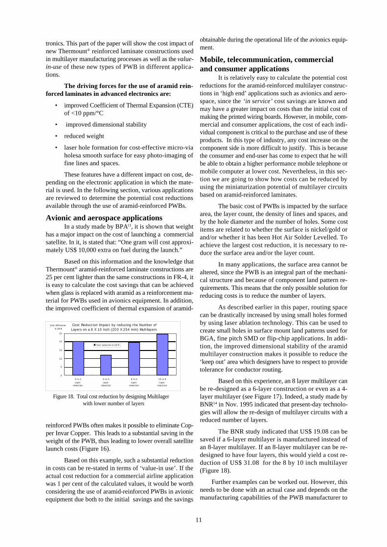
Based on this experience, an 8 layer multilayer canbe re-designed as a 6-layer construction or even as a 4-layer multilayer (see Figure 17). Indeed, a study made byBNR14 in Nov. 1995 indicated that present-day technolo-gies will allow the re-design of multilayer circuits with areduced number of layers.
The BNR study indicated that US$ 19.08 can besaved if a 6-layer multilayer is manufactured instead ofan 8-layer multilayer. If an 8-layer multilayer can be re-designed to have four layers, this would yield a cost re-duction of US$ 31.08 for the 8 by 10 inch multilayer(Figure 18).
Further examples can be worked out. However, thisneeds to be done with an actual case and depends on themanufacturing capabilities of the PWB manufacturer to
Cost differecne in US $
0
5
10
15
20
25
4 to 2Layer
reduction
6 to 4Layer
reduction
8 to 6Layer
reduction
10 to 8Layer
reduction
Cost reduction in US $
Cost Reduction Impact by reducing the Number of Layers on a 8 X 10 inch (203 X 254 mm) Multilayers
Figure 18. Total cost reduction by designing Multilagerwith lower number of layers

12
work with the new materials and processes. If cost reduc-tion is required, the use of laser technology to form smallholes, combined with the improved dimensional stabilityof aramid-reinforced laminates, offers considerable po-tential for helping to achieving this.
SummaryLaser ablated micro-vias in nonwoven aramid re-
inforced substrates provide an efficient method of inter-connecting high density chips with ultra small <0.010”(250 µm) holes and <0.020” (500 µm) stop-pads. Thistechnology can be produced using standard fabricationprocesses with minimal equipment investment. By re-ducing layers in multilayer PWBs, lowering drilling costs,and increasing real estate for routing lines, laser ablatedmicro-vias offer significant cost savings.
To fully extract the performance advantages ofnonwoven aramid PWBs and obtain lower cost, new prod-uct designs will need to be developed. Co-operation be-tween materials suppliers, advanced fabricators, and de-signers will lead to the most effective use of these newtechnologies in a broad number of applications.
BiographiesMichael Weinhold was born in the Federal Repub-
lic of Germany, where he obtained qualifications in Busi-ness Economics and Engineering. Mr. Weinhold hasworked in the printed circuit industry since 1964. He is amember of the Board of Directors of the European Insti-tute of Printed Circuits (EIPC). He represents Switzer-land at the IEC TC 52 and TC 91 committees, writingstandards for the PCB fabrication and assembly industry.He is a founder of the ICDA (the International CircuitDesigners Association). Since joining DuPont in 1970,Mr. Weinhold has held various technical and product mar-keting assignments with the “RISTON” Products Divi-sion. He is currently Product Application Manager, wherehis work relates to the latest developments in new Aramidlaminate reinforcements, PWB image transfer technolo-gies, as well as in SMD fine pitch, BGA and Flip Chipcomponent soldering technologies.
David J. Powell is a Senior Development Engineerwith the DuPont Company, Wilmington, DE. Since ob-taining a B.S. degree in Chemistry from Bates College,he has accumulated fifteen years of manufacturing, engi-neering, and development experience in the printed wir-ing board industry. He is presently working on the devel-opment of new nonwoven aramid reinforcements for lami-nates and prepregs. Mr. Powell is a member of the NorthEast Circuits Association, ISHM, and the IPC.
Bibliography1. ‘C4 Packaging for CMOS ASICs’, Matt Nowak
and John Nelson, Assembly Magazine, August1995, p. 9
2. ‘Chip-Scale Packaging and Assembly’, J. S.Hwang, SMT Magazine, July 1995, p. 17
3. ‘Blind Vias: Demands, Challenges and Solutions’,Paul Waldner, Multiline Europa, D, IEC Confer-ence, May 1995
4. ‘Vias in Pads’, Curtis Hart, Circuits AssemblyMagazine, February 1995, p. 42
5. ‘CO2 Lasers Take the Low-Power Route’, PeterGwynne, Photonics Spectra Magazine, December1994, p.104
6. ‘Laminate Technology Update for Multichip Mod-ules’, Jim Trent, Motorola SPS, Electronic Pack-aging and Production, July 1995, p. 39
7. ‘Fabricating PWBs and MCM-Ls with a NewNonwoven Aramid Reinforcement’, D.J. Powell,DuPont Fibers, Surface Mount InternationalTechnical Conference, September 1993
8. ‘Nonwoven Aramid - A Cost-effective SurfaceMount Laminate Reinforcement’, M.P. Zussmanand D.J. Powell, DuPont Fibers, Journal of Sur-face Mount Technology, October 1992.
9. ‘High Density Packaging: Micro-vias with the UVLaser’, Alan Cable and Mark Owen, SMT Maga-zine, July 1995, p. 30
10. ‘Small Via Generation’, J.M. Morrison, T.G.Tessier, B. Gu, Advanced Packaging Magazine,November/December 1994, p.26
11. ‘Laser Via Technologies for High Density MCM-L Fabrication’, Joan Tourne, Mommers Print Serv-ice B.V., ISHM Conference, April 1995
12. ‘Preliminary Process Guide for DuPontThermount® Nonwoven Aramid Reinforcement’,DuPont Advanced Fibre Systems, H-46299, De-cember 1993.
13. EIPC Marketing Meeting in Zürich, Switzer-land,1992. ‘Trends and Developments in the Elec-tronic Industry’ presented by Roger L. Tyler, Sen-ior Consultant, BPA
14. ‘The Cost Impact on PWB Design using AramidTechnology Options’, by M. Cotton, presentedduring the First European Aramid Forum, at BNREurope Limited, London Road, Harlow, EssexCM17 9NA, England, on November 2nd and 3rd,1995.