Fabrication of CMOS Integrated Circuitsee434/Handouts/03-Fabrication.pdf · CMOS Fabrication...
34
Fabrication of CMOS Integrated Circuits Dae Hyun Kim EECS Washington State University
Transcript of Fabrication of CMOS Integrated Circuitsee434/Handouts/03-Fabrication.pdf · CMOS Fabrication...
Fabrication of CMOS Integrated Circuits
Dae Hyun Kim
EECS Washington State University

References
• John P. Uyemura, “Introduction to VLSI Circuits and Systems,” 2002. – Chapter 4

Goal
• Understand the fabrication (manufacturing) process for CMOS integrated circuits (ICs)
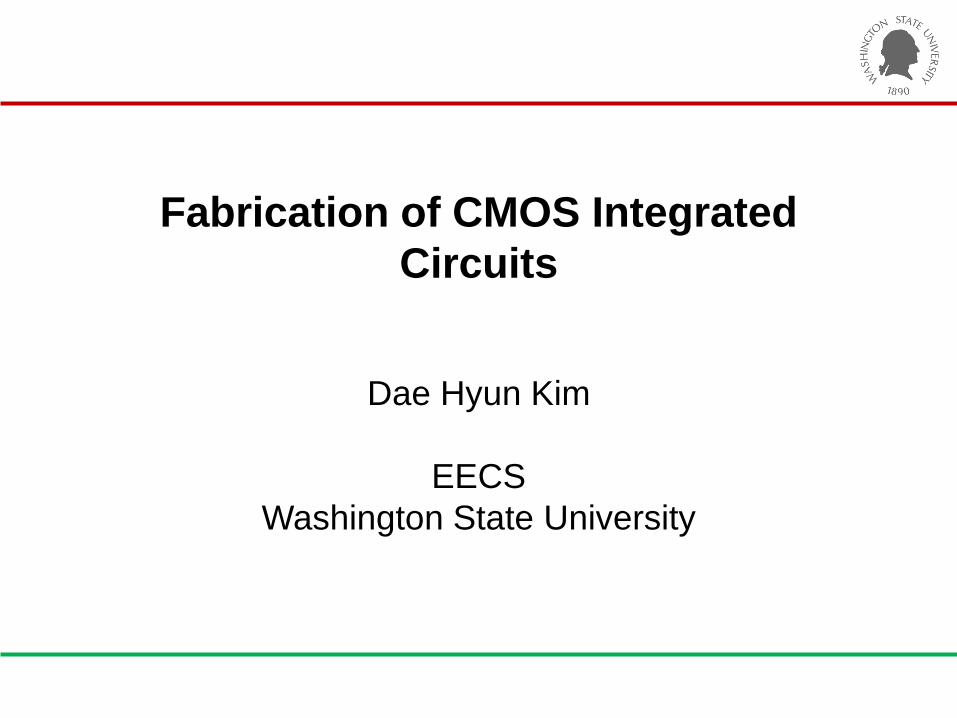
Silicon Wafer and Yield
• Yield – 𝑌𝑌 = 𝑁𝑁𝐺𝐺
𝑁𝑁𝑇𝑇× 100%
• 𝑁𝑁𝐺𝐺: # good dies • 𝑁𝑁𝑇𝑇: # total dies
– 𝑁𝑁𝑇𝑇 = 𝜋𝜋 (𝑑𝑑−𝑑𝑑𝑒𝑒)2
4𝐴𝐴𝑑𝑑𝑑𝑑𝑒𝑒
– 𝑌𝑌 = 𝑒𝑒− 𝐷𝐷𝐴𝐴 • 𝐴𝐴: die area • 𝐷𝐷: defect density
– 𝑌𝑌 = 1 − 𝐴𝐴𝑑𝑑𝑑𝑑𝑒𝑒𝐷𝐷𝑐𝑐
𝑐𝑐
– 𝑌𝑌 = 1
1+𝐴𝐴𝑑𝑑𝑑𝑑𝑒𝑒𝐷𝐷
𝑐𝑐
2
• 𝑐𝑐: a constant for clustered defects
Source: http://www.chipsetc.com/uploads/1/2/4/4/1244189/1780324_orig.jpg
Diameter
Die

Material Growth and Deposition
• Doped silicon layers – Ion implantation – Annealing
ion beam
n+
heating
Silicon

Material Growth and Deposition
• Silicon Dioxide (insulator) – Thermal oxide
– Chemical vapor deposition (CVD) oxide
Silicon
O2 flow SiO2 layer
Silicon
SiO2 molecules
SiO2 layer
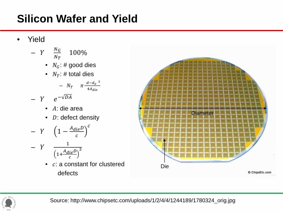
Material Growth and Deposition
• Polycrystal Silicon – Used to fabricate Gate – Deposition
• Metal – Deposition
G
n+ n+
G
p

Material Growth and Deposition
• Silicon Nitride – Barrier on the topmost layer
• Barrier is also used for preventing copper from diffusing into
adjacent layers.
n+ n+
G
p
barrier
inter-layer dielectric (ILD)

Material Growth and Deposition
• Chemical-Mechanical Polishing (CMP) – also called Chemical-Mechanical Planarization – After depositing each layer, CMP is applied to planarize the surface.
Source: http://www.ntu.edu.sg/home/mdlbutler/Research/cmp%20polisher.jpg Source: http://linx-consulting.com/images/planarized_IC.gif

Lithography (Photolithography)
• Reticle (mask)
Source: https://upload.wikimedia.org/wikipedia/commons/thumb/5/5e/ Mask_illustration.svg/220px-Mask_illustration.svg.png
Silicon
Masking film
Photoresist Mask glass Mask
UV
Exposure/ Development/ Rinsing
Etching Stripping

CMOS Fabrication Process
p+ substrate
p-epi

CMOS Fabrication Process
Gate-oxide deposition
SiO2
p+ substrate
p-epi

CMOS Fabrication Process
Photoresist
SiO2
p+ substrate
p-epi
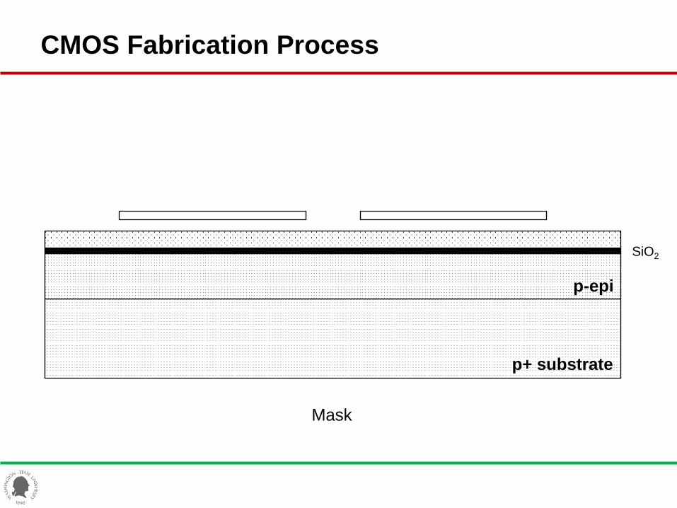
CMOS Fabrication Process
Mask
SiO2
p+ substrate
p-epi

CMOS Fabrication Process
Expose (photolithography)
SiO2
p+ substrate
p-epi

CMOS Fabrication Process
After photolithography
SiO2
p+ substrate
p-epi

CMOS Fabrication Process
Remove mask
SiO2
p+ substrate
p-epi

CMOS Fabrication Process
Etching
p+ substrate
p-epi

CMOS Fabrication Process
Etching
p+ substrate
p-epi
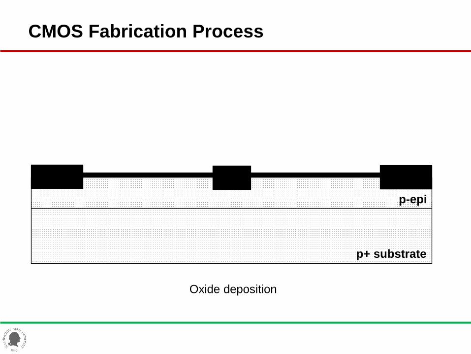
CMOS Fabrication Process
Oxide deposition
p+ substrate
p-epi
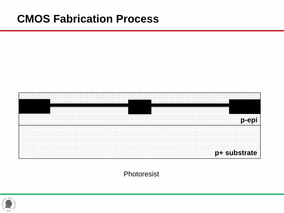
CMOS Fabrication Process
Photoresist
p+ substrate
p-epi

CMOS Fabrication Process
Mask
p+ substrate
p-epi

CMOS Fabrication Process
Photolithography
p+ substrate
p-epi

CMOS Fabrication Process
After photolithography
p+ substrate
p-epi

CMOS Fabrication Process
Etching
p+ substrate
p-epi
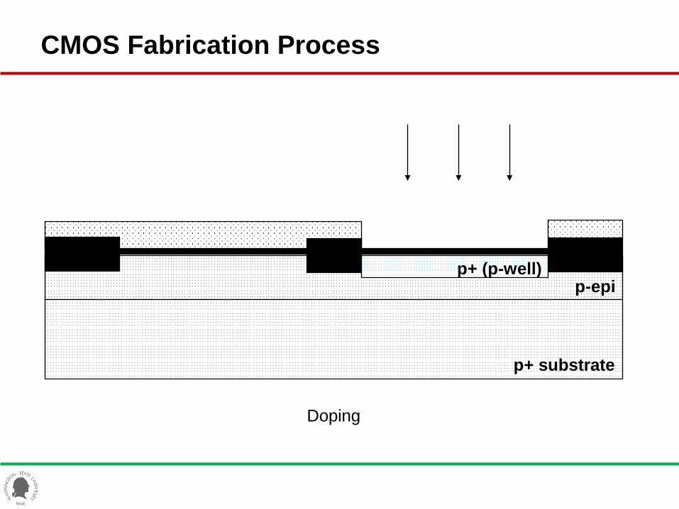
CMOS Fabrication Process
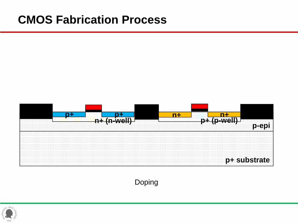
Doping
p+ substrate
p-epi p+ (p-well)

CMOS Fabrication Process
Doping
p+ substrate
p-epi p+ (p-well) n+ (n-well)

CMOS Fabrication Process
Poly
p+ substrate
p-epi p+ (p-well) n+ (n-well)

CMOS Fabrication Process
Etching
p+ substrate
p-epi p+ (p-well) n+ (n-well)
CMOS Fabrication Process
p+ substrate
p-epi p+ (p-well) n+ (n-well)
Doping
p+ p+ n+ n+

CMOS Fabrication Process
p+ substrate
p-epi p+ (p-well) n+ (n-well)
Oxide deposition
p+ n+ n+
SiO2
p+

CMOS Fabrication Process
p+ substrate
p-epi p+ (p-well) n+ (n-well)
Contact
p+ n+ n+
SiO2
contact
p+

CMOS Fabrication Process
p+ substrate
p-epi p+ (p-well) n+ (n-well)
p+ n+ n+
SiO2
contact
p+
Metal 1

CMOS Fabrication Process
p+ substrate
p-epi p+ (p-well) n+ (n-well)
p+ n+ n+
SiO2
contact
p+
Via12

![CMOS Fabrication [Compatibility Mode]](https://static.fdocuments.in/doc/165x107/577cdf861a28ab9e78b17027/cmos-fabrication-compatibility-mode.jpg)