
EE 330 Lecture 31 - Iowa State Universityclass.ece.iastate.edu/ee330/lectures/EE 330 Lect 31 Fall...
58
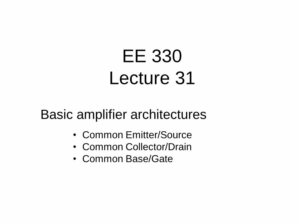
EE 330 Lecture 31 Basic amplifier architectures • Common Emitter/Source • Common Collector/Drain • Common Base/Gate
Transcript of EE 330 Lecture 31 - Iowa State Universityclass.ece.iastate.edu/ee330/lectures/EE 330 Lect 31 Fall...
EE 330
Lecture 31
Basic amplifier architectures
• Common Emitter/Source
• Common Collector/Drain
• Common Base/Gate
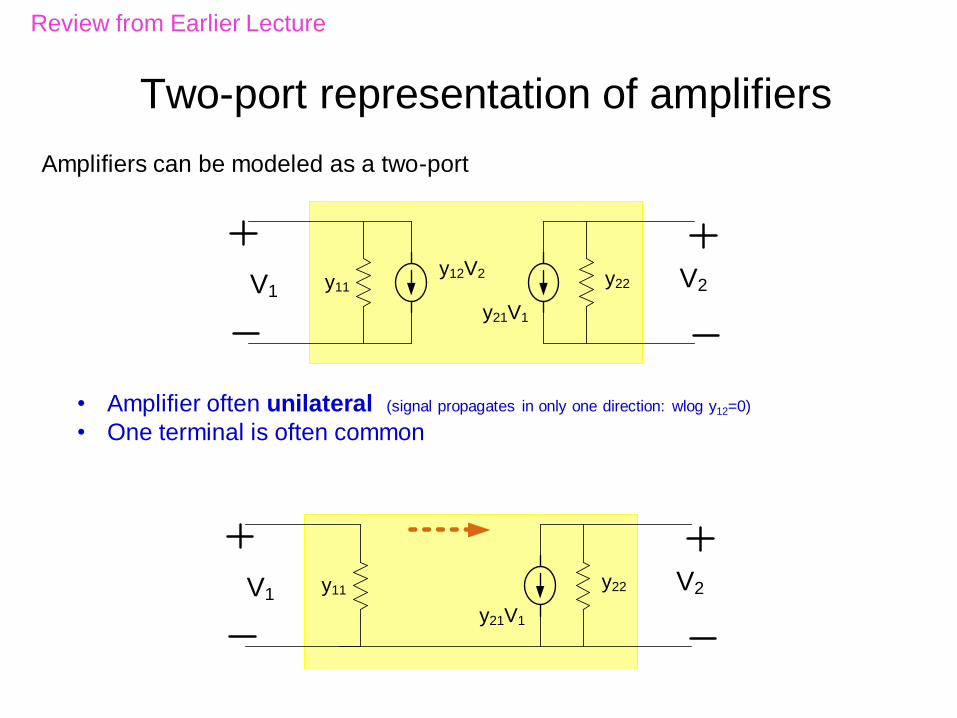
Two-port representation of amplifiers
y11y22 V2
y21V1
y12V2V1
Amplifiers can be modeled as a two-port
• Amplifier often unilateral (signal propagates in only one direction: wlog y12=0)
• One terminal is often common
y11y22 V2
y21V1
V1
Review from Earlier Lecture
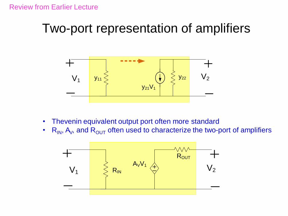
Two-port representation of amplifiers
RINV2
AVV1
V1
ROUT
• Thevenin equivalent output port often more standard
• RIN, AV, and ROUT often used to characterize the two-port of amplifiers
y11y22 V2
y21V1
V1
Review from Earlier Lecture
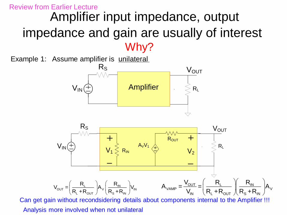
Amplifier input impedance, output
impedance and gain are usually of interest
Example 1: Assume amplifier is unilateral
VIN
RS
Amplifier RL
VOUT
RIN V2
AVV1
V1
ROUT
VIN
RS
RL
VOUT
L INOUT V IN
L OUT S IN
R RV = A V
R +R R +R
OUT L INVAMP V
IN L OUT S IN
V R RA = = A
V R +R R +R
Can get gain without recondsidering details about components internal to the Amplifier !!!
Why?
Analysis more involved when not unilateral
Review from Earlier Lecture
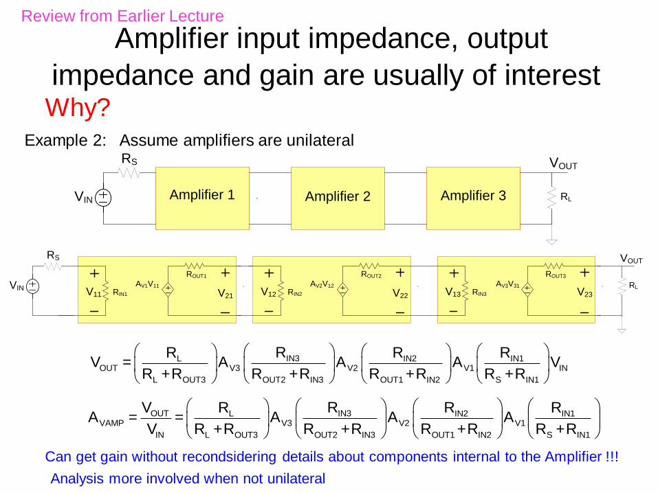
Amplifier input impedance, output
impedance and gain are usually of interest
Example 2: Assume amplifiers are unilateral
Can get gain without recondsidering details about components internal to the Amplifier !!!
Why?
VIN
RS
Amplifier 1 Amplifier 2 Amplifier 3 RL
VOUT
RIN1 V21
AV1V11
V11
ROUT1
VIN
RS
RIN2 V22
AV2V12
V12
ROUT2
RIN3 V23
AV3V31
V13
ROUT3
RL
VOUT
IN3L IN2 IN1OUT V3 V2 V1 IN
L OUT3 OUT2 IN3 OUT1 IN2 S IN1
RR R RV = A A A V
R +R R +R R +R R +R
OUT IN3L IN2 IN1VAMP V3 V2 V1
IN L OUT3 OUT2 IN3 OUT1 IN2 S IN1
V RR R RA = = A A A
V R +R R +R R +R R +R
Analysis more involved when not unilateral
Review from Earlier Lecture
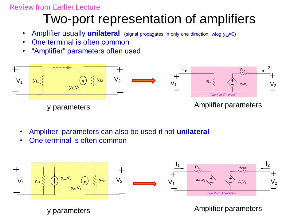
Two-port representation of amplifiers
y11y22 V2
y21V1
y12V2V1
• Amplifier usually unilateral (signal propagates in only one direction: wlog y12=0)
• One terminal is often common
• “Amplifier” parameters often used
y11y22 V2
y21V1
V1 V1 V2
I1 I2
RIN
ROUT
AVV1
Two Port (Thevenin)
V1 V2
I1 I2RIN ROUT
AVV1AVRV2
Two Port (Thevenin)
• Amplifier parameters can also be used if not unilateral
• One terminal is often common
y parameters Amplifier parameters
y parameters Amplifier parameters
Review from Earlier Lecture
V1 V2
I1 I2RIN ROUT
AVV1AVRV2
Two Port (Thevenin)
y11A y22A
y12AV2A
y21AV1A
V1A V2A
i1Ai2A
R1
RB
V1B V2B
I1B I2B
g22B
g21BV2B g12BV1B
g11B
Two Port (Norton)
i1C
Linear Two Port
v1C
i2C
v2C
H-parameters
(Hybrid Parameters)
1 11 1 12 2C C C C Ch h V i v
2 21 1 22 2C C C C Ch h i i v
RXX
V1
i1
V2
i2
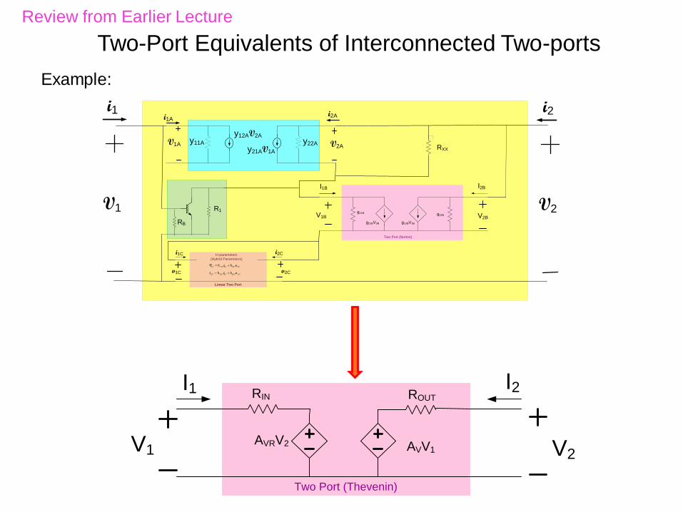
Two-Port Equivalents of Interconnected Two-ports
Example:
Review from Earlier Lecture
Determination of Amplifier Two-Port Parameters
• Input and output parameters are obtained in exactly the same way,
only distinction is in the notation used for the ports.
• Methods given for obtaining amplifier parameters Rin, ROUT and AV for
unilateral networks are a special case of the non-unilateral analysis by
observing that AVR=0.
• In some cases, other methods for obtaining the amplifier paramaters
are easier than what was just discussed
Review from Earlier Lecture
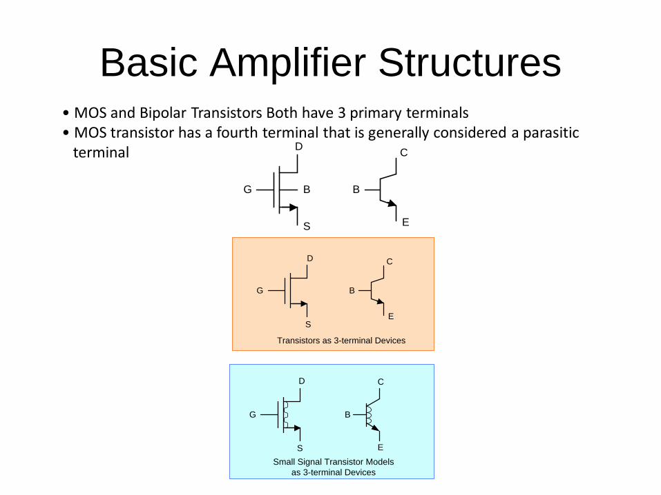
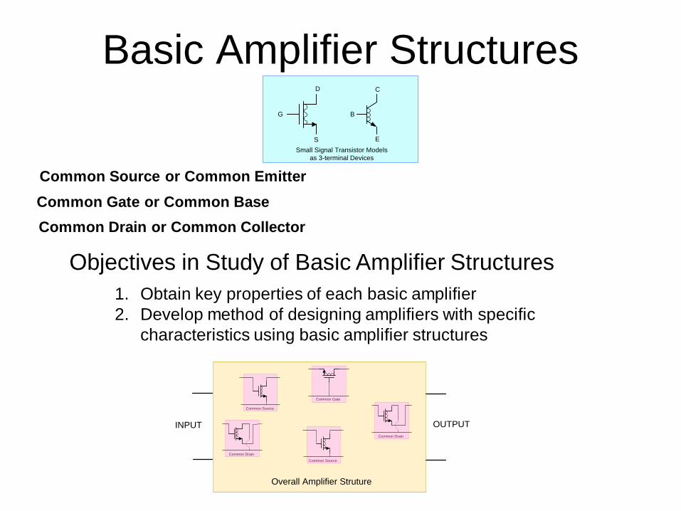
Basic Amplifier Structures• MOS and Bipolar Transistors Both have 3 primary terminals• MOS transistor has a fourth terminal that is generally considered a parasitic
terminal D
G B
S
B
E
C
D
G
S
B
E
C
Transistors as 3-terminal Devices
D
S
G B
E
C
Small Signal Transistor Models
as 3-terminal Devices
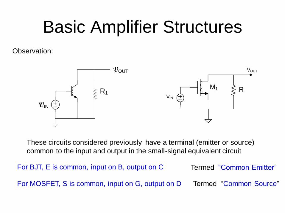
Basic Amplifier Structures
R1
VIN
VOUT
RM1
VIN
VOUT
These circuits considered previously have a terminal (emitter or source)
common to the input and output in the small-signal equivalent circuit
Observation:
For BJT, E is common, input on B, output on C
For MOSFET, S is common, input on G, output on D
Termed “Common Emitter”
Termed “Common Source”
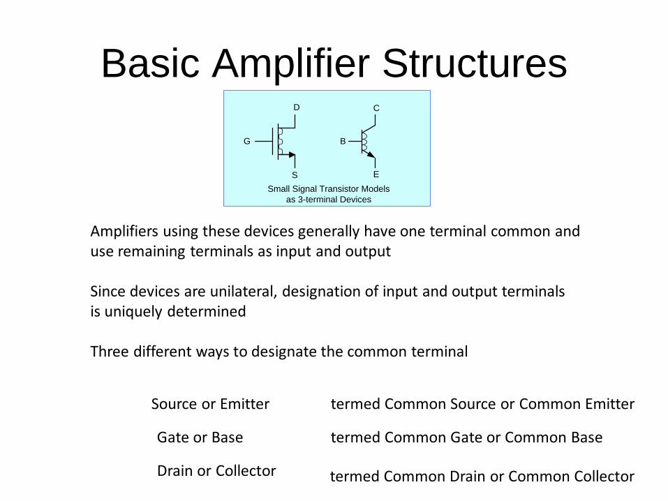
Basic Amplifier Structures
Amplifiers using these devices generally have one terminal common and use remaining terminals as input and output
Since devices are unilateral, designation of input and output terminalsis uniquely determined
Three different ways to designate the common terminal
Source or Emitter
Gate or Base
Drain or Collector
termed Common Source or Common Emitter
termed Common Gate or Common Base
termed Common Drain or Common Collector
D
S
G B
E
C
Small Signal Transistor Models
as 3-terminal Devices
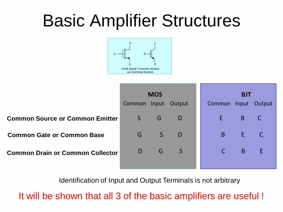
Basic Amplifier Structures
Common Source or Common Emitter
Common Gate or Common Base
Common Drain or Common Collector
Common Input Output Common Input Output
S G D E B C
G S D B E C
D G S C B E
MOS BJT
D
S
G B
E
C
Small Signal Transistor Models
as 3-terminal Devices
It will be shown that all 3 of the basic amplifiers are useful !
Identification of Input and Output Terminals is not arbitrary
Basic Amplifier Structures
Common Source or Common Emitter
Common Gate or Common Base
Common Drain or Common Collector
D
S
G B
E
C
Small Signal Transistor Models
as 3-terminal Devices
Objectives in Study of Basic Amplifier Structures
1. Obtain key properties of each basic amplifier
2. Develop method of designing amplifiers with specific
characteristics using basic amplifier structures
Common Source
Common Source
Common Gate
Common Drain
Common Drain
INPUT OUTPUT
Overall Amplifier Struture
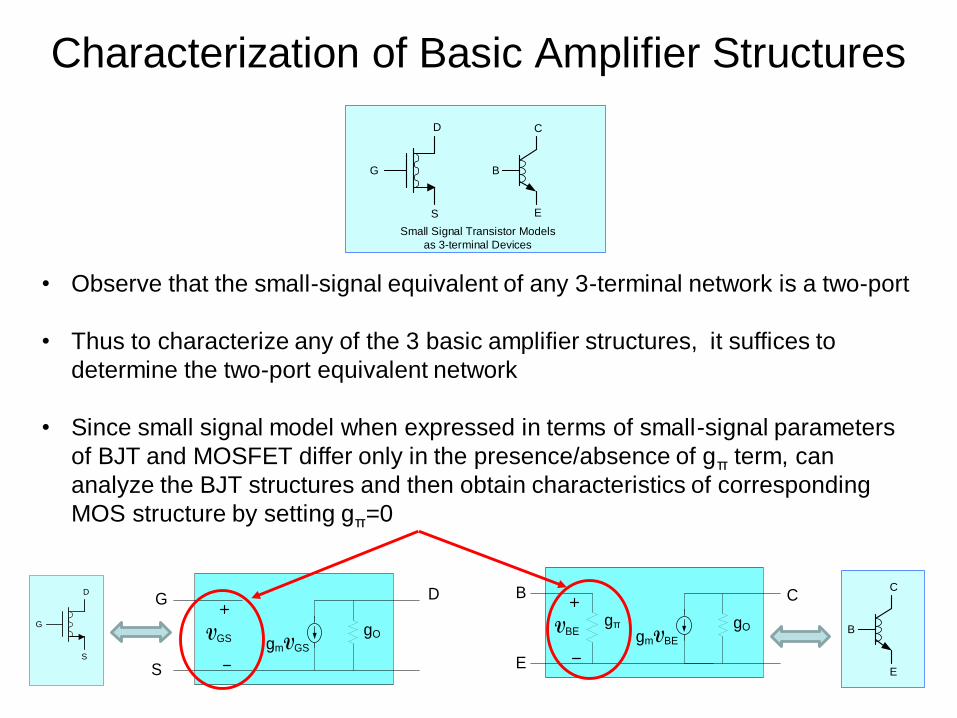
Characterization of Basic Amplifier Structures
D
S
G B
E
C
Small Signal Transistor Models
as 3-terminal Devices
• Observe that the small-signal equivalent of any 3-terminal network is a two-port
• Thus to characterize any of the 3 basic amplifier structures, it suffices to
determine the two-port equivalent network
• Since small signal model when expressed in terms of small-signal parameters
of BJT and MOSFET differ only in the presence/absence of gπ term, can
analyze the BJT structures and then obtain characteristics of corresponding
MOS structure by setting gπ=0
gOgmVGS
VGS
G D
S
gOgmVBE
VBEgπ
B
E
CD
S
GB
E
C
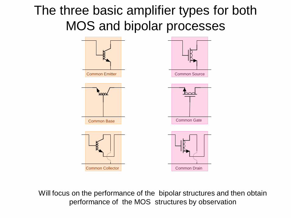
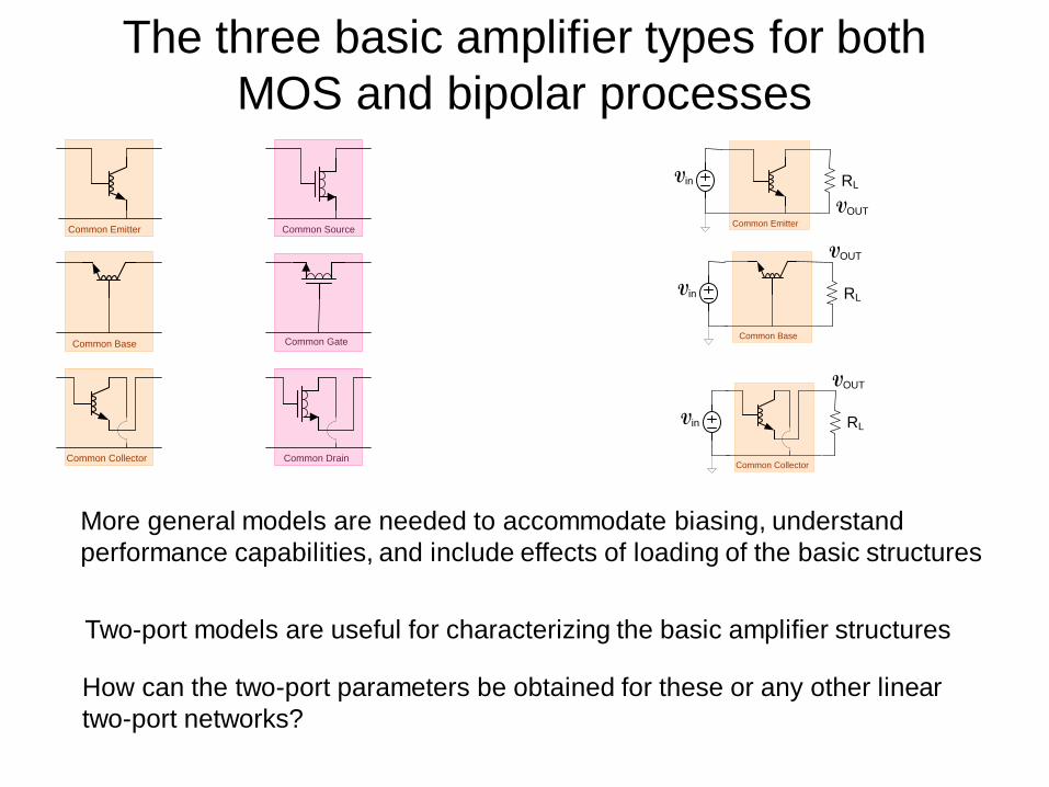
The three basic amplifier types for both
MOS and bipolar processes
Common Emitter
Common Base
Common Collector
Common Source
Common Gate
Common Drain
Will focus on the performance of the bipolar structures and then obtain
performance of the MOS structures by observation
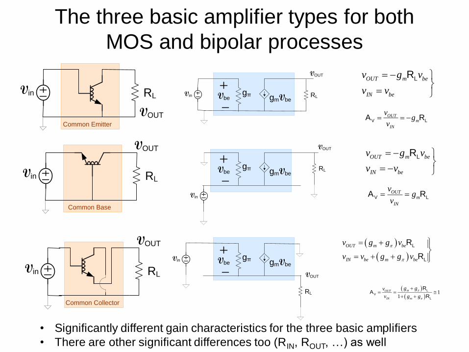
The three basic amplifier types for both
MOS and bipolar processes
Common Emitter
Vin
VOUT
RL
Common Base
Vin RL
VOUT
Common Collector
Vin RL
VOUT
Vbe gmVbegπ
Vbe gmVbegπ
Vbe gmVbegπ
VOUT
RLVin
Vin
VOUT
RL
Vin
RL
VOUT
LROUT m be
IN be
v g v
v v
V LA ROUTm
IN
vg
v
LROUT m be
IN be
v g v
v v
V LA ROUTm
IN
vg
v
L
L
R
R
OUT m be
IN be m be
v g g v
v v g g v
1
1
L
V
L
RA
R
mOUT
IN m
g gv
v g g
• Significantly different gain characteristics for the three basic amplifiers
• There are other significant differences too (RIN, ROUT, …) as well
The three basic amplifier types for both
MOS and bipolar processes
Common Emitter
Common Base
Common Collector
Common Source
Common Gate
Common Drain
How can the two-port parameters be obtained for these or any other linear
two-port networks?
More general models are needed to accommodate biasing, understand
performance capabilities, and include effects of loading of the basic structures
Two-port models are useful for characterizing the basic amplifier structures
Common Emitter
Vin
VOUT
RL
Common Base
Vin RL
VOUT
Common Collector
Vin RL
VOUT
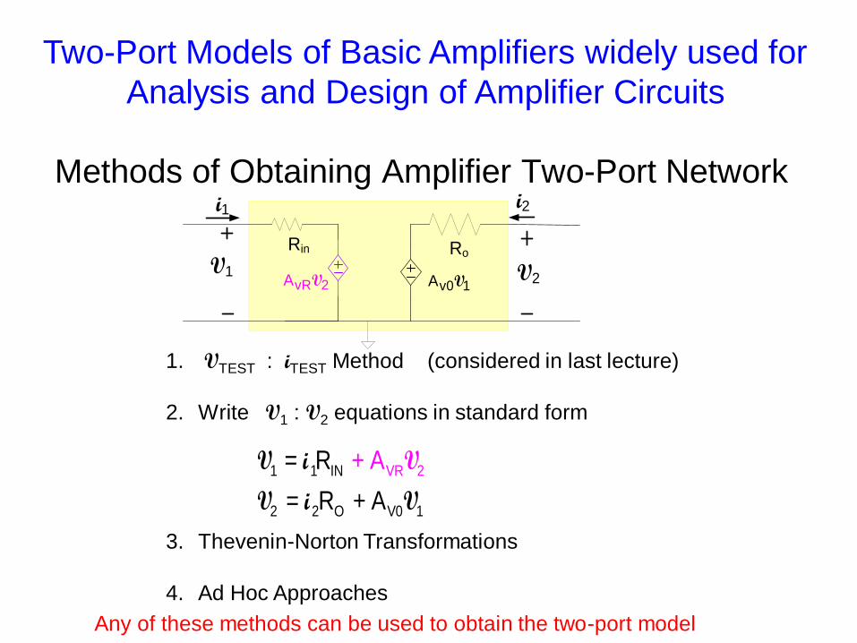
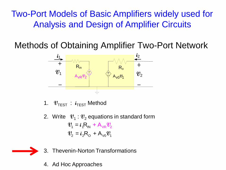
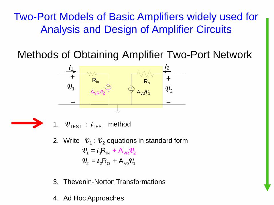
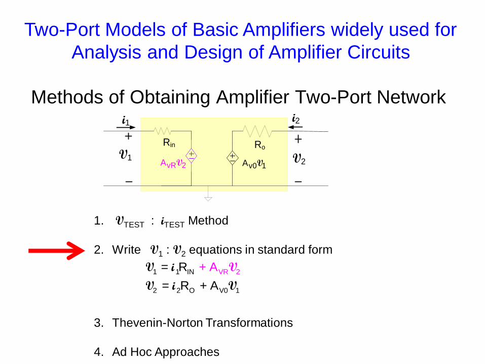
Methods of Obtaining Amplifier Two-Port Network
1. VTEST : iTEST Method (considered in last lecture)
2. Write V1 : V2 equations in standard form
3. Thevenin-Norton Transformations
4. Ad Hoc Approaches
Ro
V1
i1
v0 1A V V2
Rin
i2
vR 2A V
VR 2 1 1 IN
2 2 O V0 1
= R
= R +
A
A
+ V i V
V i V
Two-Port Models of Basic Amplifiers widely used for
Analysis and Design of Amplifier Circuits
Any of these methods can be used to obtain the two-port model
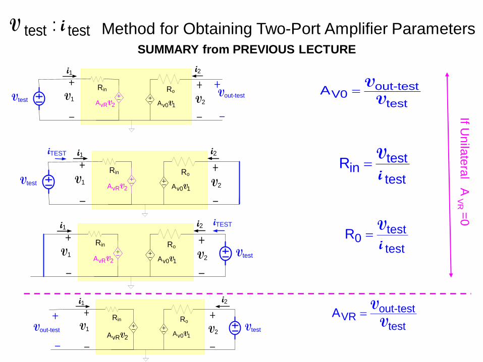
testin
test
R V
i
Ro
V1
i1
v0 1A VV2
Rin
i2
vR 2A VVtestVout-test
out-testVR
test
A V
V
test0
test
R V
i
out-testV0
test
A V
V
Ro
V1
i1
v0 1A V V2
Rin
i2
vR 2A VVtest
iTEST
Ro
V1
i1
v0 1A V V2
Rin
i2
vR 2A VVtest
Vout-test
Ro
V1
i1
v0 1A V V2
Rin
i2
vR 2A VVtest
iTEST
test test: V i Method for Obtaining Two-Port Amplifier Parameters
SUMMARY from PREVIOUS LECTURE
If Un
ilate
ral A
VR
=0
Common Emitter
Common Base
Common Collector
Common Source
Common Gate
Common Drain
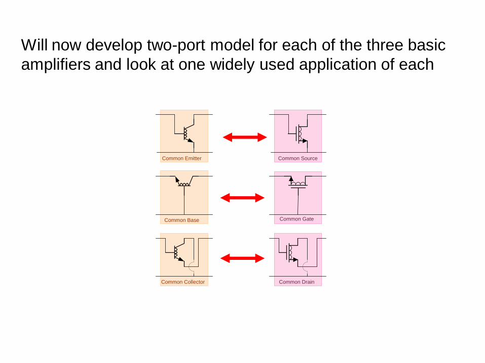
Will now develop two-port model for each of the three basic
amplifiers and look at one widely used application of each
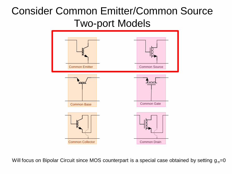
Consider Common Emitter/Common Source
Two-port Models
Common Emitter
Common Base
Common Collector
Common Source
Common Gate
Common Drain
Will focus on Bipolar Circuit since MOS counterpart is a special case obtained by setting gπ=0
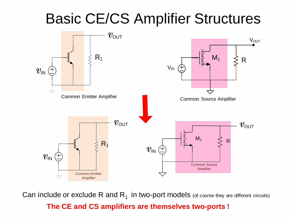
Basic CE/CS Amplifier Structures
R1
VIN
VOUT
RM1
VIN
VOUT
The CE and CS amplifiers are themselves two-ports !
Common Emitter AmplifierCommon Source Amplifier
R1
VIN
VOUT
RM1
VOUT
VIN
Common Emitter
Amplifier
Common Source
Amplifier
Can include or exclude R and R1 in two-port models (of course they are different circuits)
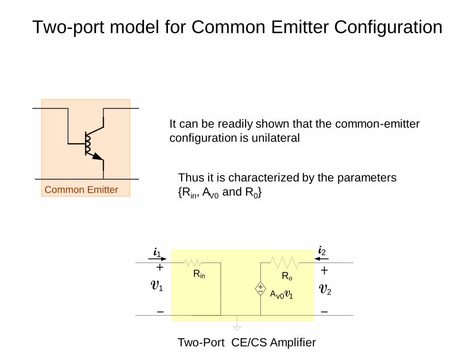
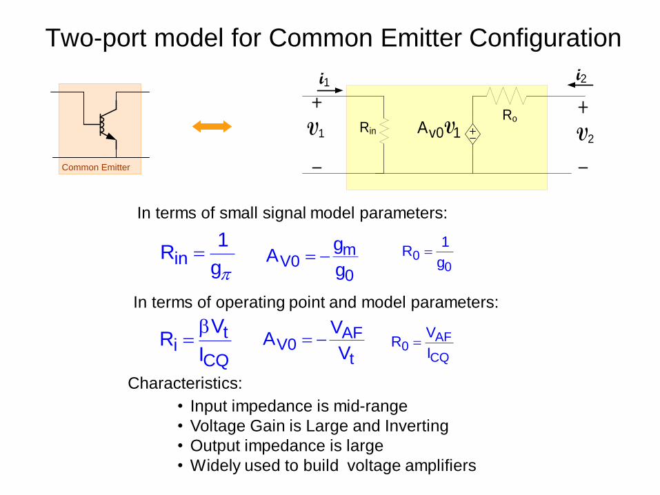
Two-port model for Common Emitter Configuration
Common EmitterThus it is characterized by the parameters
{Rin, AV0 and R0}
It can be readily shown that the common-emitter
configuration is unilateral
Ro
V1
i1
v0 1A V V2
Rin
i2
Two-Port CE/CS Amplifier
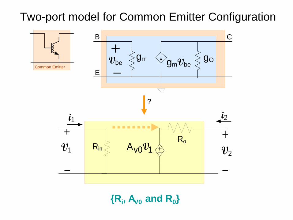
Two-port model for Common Emitter Configuration
Common Emitter
VbegOgmVbe
gπ
B
E
C
Ro
V1
i1
v0 1A V V2Rin
i2
{Ri, AV0 and R0}
?
Methods of Obtaining Amplifier Two-Port Network
1. VTEST : iTEST Method
2. Write V1 : V2 equations in standard form
3. Thevenin-Norton Transformations
4. Ad Hoc Approaches
Ro
V1
i1
v0 1A V V2
Rin
i2
vR 2A V
VR 2 1 1 IN
2 2 O V0 1
= R
= R +
A
A
+ V i V
V i V
Two-Port Models of Basic Amplifiers widely used for
Analysis and Design of Amplifier Circuits
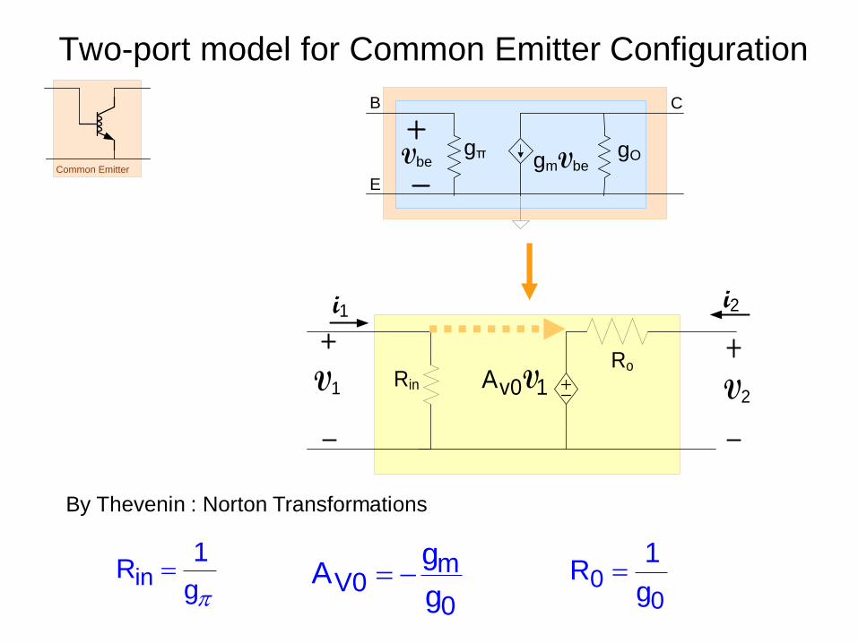
Two-port model for Common Emitter Configuration
Common EmitterVbe
gOgmVbegπ
B
E
C
Ro
V1
i1
v0 1A V V2Rin
i2
By Thevenin : Norton Transformations
in1
Rg
mV0
0
gA
g 0
0
1R
g
Methods of Obtaining Amplifier Two-Port Network
1. VTEST : iTEST method
2. Write V1 : V2 equations in standard form
3. Thevenin-Norton Transformations
4. Ad Hoc Approaches
Ro
V1
i1
v0 1A V V2
Rin
i2
vR 2A V
VR 2 1 1 IN
2 2 O V0 1
= R
= R +
A
A
+ V i V
V i V
Two-Port Models of Basic Amplifiers widely used for
Analysis and Design of Amplifier Circuits
Two-port model for Common Emitter Configuration
Common Emitter
Ro
V1
i1
v0 1A V V2Rin
i2
{Rin, AV0 and R0}
itest
Vtest VbegOgmVbe
gπ
testin
test
R V
i
in1
Rg
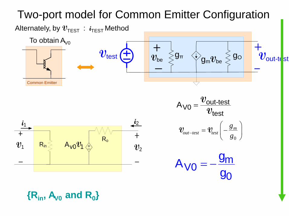
To obtain Rin
Alternately, by VTEST : iTEST Method
Two-port model for Common Emitter Configuration
Common Emitter
Ro
V1
i1
v0 1A V V2Rin
i2
{Rin, AV0 and R0}
To obtain AV0
Vout-testVtest Vbe
gOgmVbegπ
out-testV0
test
A V
V
0
mout test test
g
g
V V
mV0
0
gA
g
Alternately, by VTEST : iTEST Method
Two-port model for Common Emitter Configuration
Common Emitter
Ro
V1
i1
v0 1A V V2Rin
i2
{Rin, AV0 and R0}
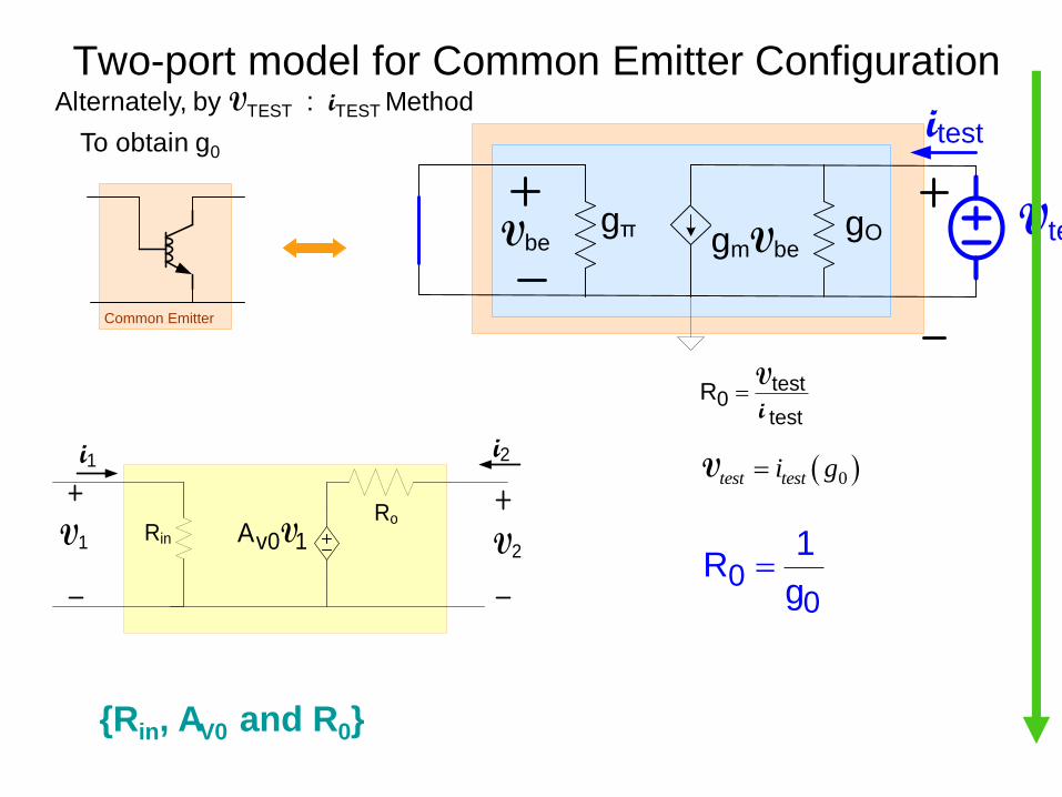
To obtain g0
0test testi gV
VbegOgmVbe
gπ
itest
Vtest
test0
test
R V
i
00
1R
g
Alternately, by VTEST : iTEST Method
Two-port model for Common Emitter Configuration
Common Emitter
Ro
V1
i1
v0 1A V V2Rin
i2
00
1R
gm
V00
gA
g in
1R
g
• Input impedance is mid-range
• Voltage Gain is Large and Inverting
• Output impedance is large
• Widely used to build voltage amplifiers
ti
CQ
VR
I
AF
V0t
VA
V AF
0CQ
VR
I
In terms of operating point and model parameters:
In terms of small signal model parameters:
Characteristics:
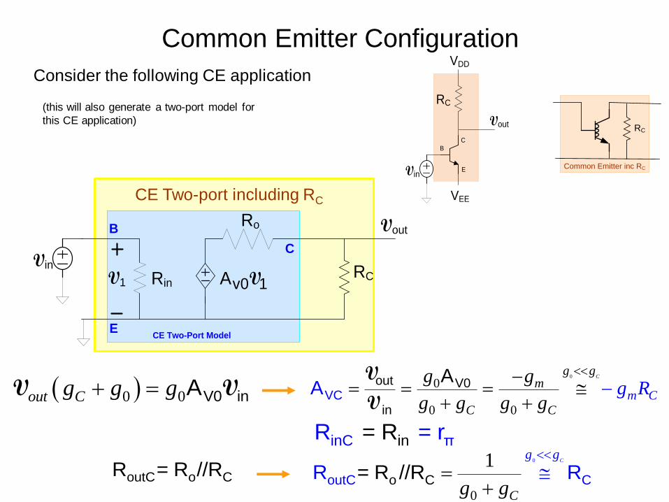
Common Emitter Configuration
Consider the following CE application
B
E
C
VDD
Vin
RC
Vout
VEE
Ro
V1 v0 1A VRin
C
B
E
RC
Vout
Vin
CE Two-Port Model
0 0 V0 inAout Cg g g V V0
0
0 0
ouC
tV
V0
in
AA
Cg g
m
C C
m C
gR
g
g g gg
g
V
V
iinC πn= RR = r
outC o CR = R //R0
0
1ou o CtC CR = R //R R
C
g
C
g
g g
CE Two-port including RC
(this will also generate a two-port model for
this CE application)
Common Emitter inc RC
RC
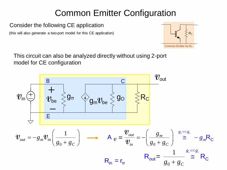
Common Emitter Configuration
Consider the following CE application
This circuit can also be analyzed directly without using 2-port
model for CE configuration
VbegOgmVbe
gπ RCVin
B
E
CVout
0
1out m in
C
gg g
V V
0
0
CA R
C
out m
in C
g g
mgg
g gV
V=
V
in πR = r
0
0
1out CR = R
Cg
C
g
g g
(this will also generate a two-port model for this CE application)
Common Emitter inc RC
RC
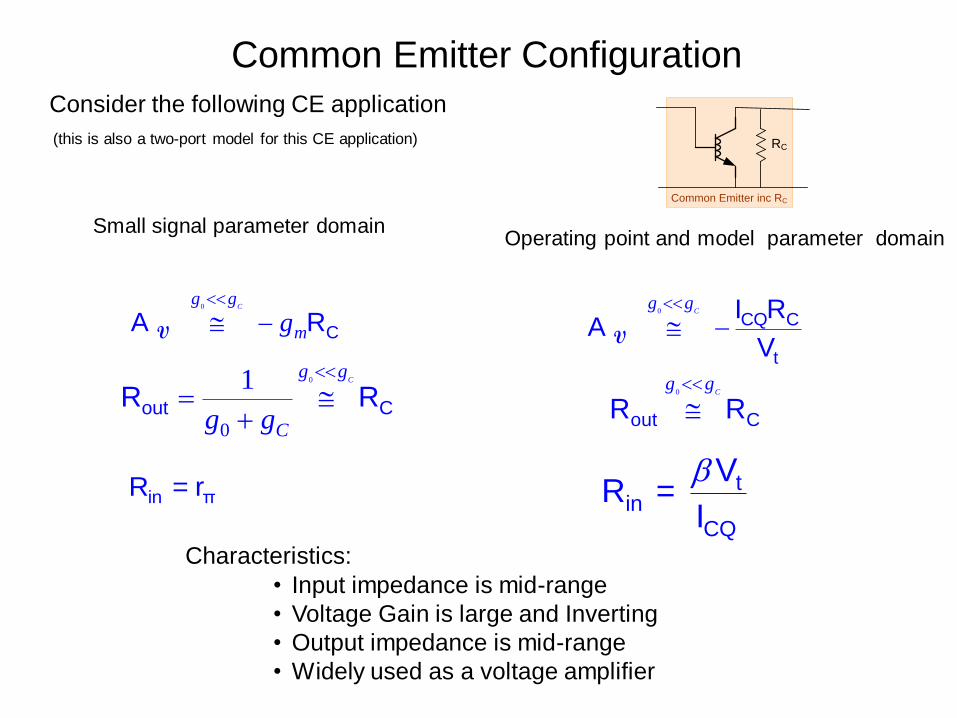
Common Emitter Configuration
Consider the following CE application
0
CA R
C
g g
mgV
in πR = r
• Input impedance is mid-range
• Voltage Gain is large and Inverting
• Output impedance is mid-range
• Widely used as a voltage amplifier
0
0
1out CR R
Cg g
Cg g
0
CQ C
t
I RA
V
C
g g
V
0
out CR R
C
g g
tin
CQ
VR =
I
(this is also a two-port model for this CE application)
Common Emitter inc RC
RC
Small signal parameter domainOperating point and model parameter domain
Characteristics:
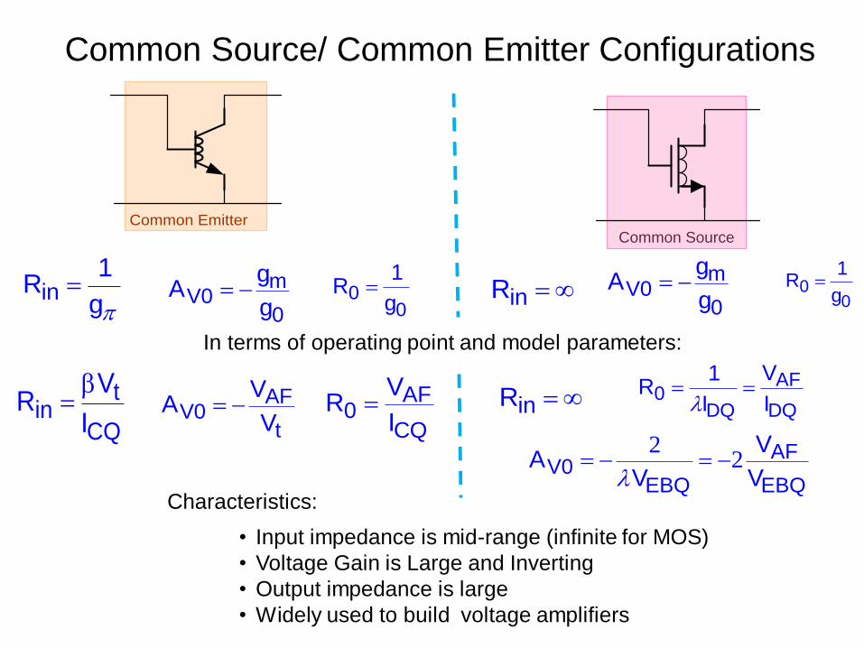
Common Source/ Common Emitter Configurations
Common EmitterCommon Source
00
1R
gm
V00
gA
g in
1R
g
tin
CQ
VR
I
AF
V0t
VA
V AF
0CQ
VR
I
In terms of operating point and model parameters:
00
1R
gm
V00
gA
g
inR
inR
22 AF
V0EBQ EBQ
VA
V V
AF0
DQ DQ
V1R
I I
• Input impedance is mid-range (infinite for MOS)
• Voltage Gain is Large and Inverting
• Output impedance is large
• Widely used to build voltage amplifiers
Characteristics:
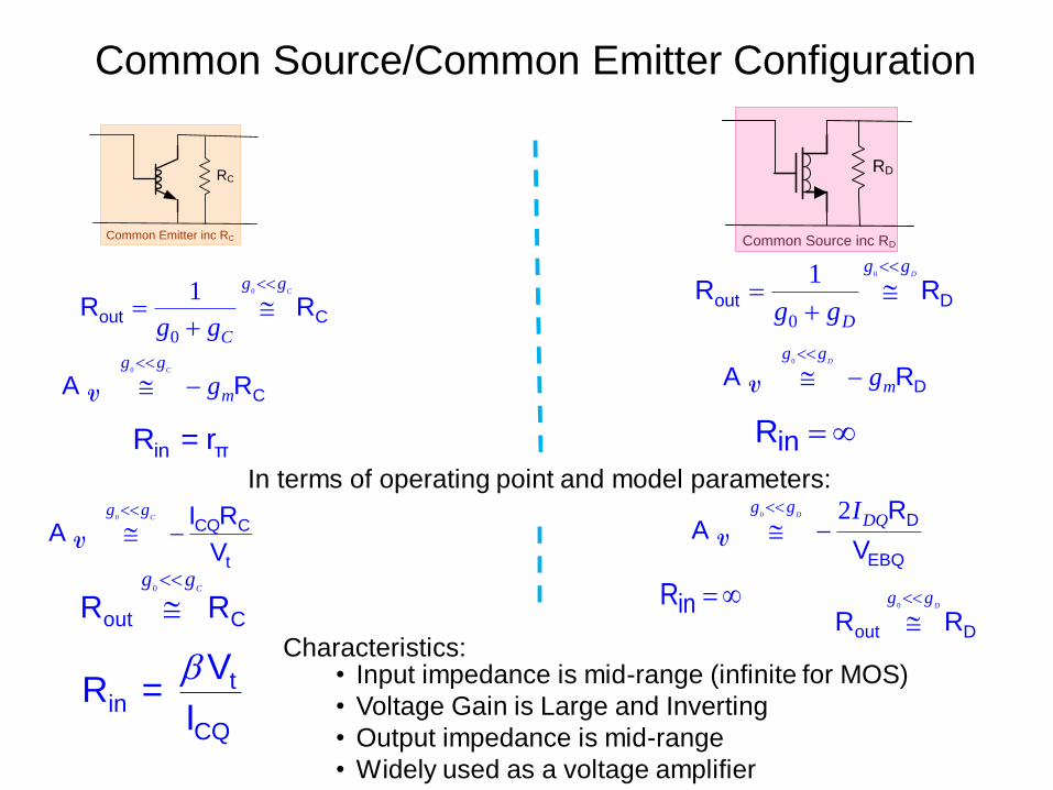
Common Source/Common Emitter Configuration
0
CA R
C
g g
mgV
in πR = r
• Input impedance is mid-range (infinite for MOS)
• Voltage Gain is Large and Inverting
• Output impedance is mid-range
• Widely used as a voltage amplifier
0
0
1out DR R
Dg g
Dg g
0
CQ C
t
I RA
V
C
g g
V
0
out CR R
C
g g
tin
CQ
VR =
I
Common Emitter inc RC
RC
Common Source inc RD
RD
In terms of operating point and model parameters:
0
0
1out CR R
Cg g
Cg g0
DA R
D
g g
mgV
inR
inR
0 2 D
EBQ
RA
V
D
g gDQI
V
0
out DR R
D
g g
Characteristics:

Consider Common Collector/Common Drain
Two-port Models
Common Emitter
Common Base
Common Collector
Common Source
Common Gate
Common Drain
Will focus on Bipolar Circuit since MOS counterpart is a special case obtained by setting gπ=0
Two-port model for Common Collector Configuration
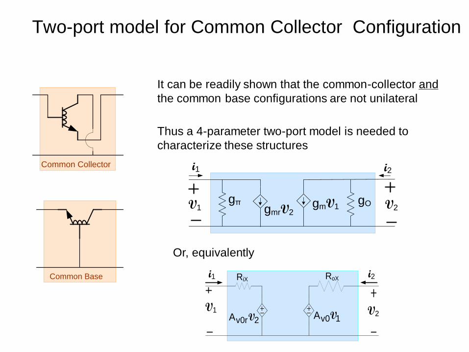
Common Collector
It can be readily shown that the common-collector and
the common base configurations are not unilateral
Thus a 4-parameter two-port model is needed to
characterize these structures
V1gOgmV1
gπgmrV2
V2
i1 i2
RoX
V1v0 1A V V2
RiXi2i1
v0r 2A V
Or, equivalently
Common Base
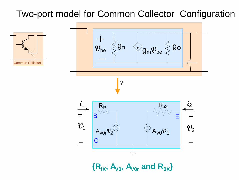
Two-port model for Common Collector Configuration
{RiX, AV0, AV0r and R0X}
?
VbegOgmVbe
gπ
Common Collector
RoX
V1v0 1A V V2
RiXi2i1
v0r 2A V
B
C
E

Methods of Obtaining Amplifier Two-Port Network
1. VTEST : iTEST Method
2. Write V1 : V2 equations in standard form
3. Thevenin-Norton Transformations
4. Ad Hoc Approaches
Ro
V1
i1
v0 1A V V2
Rin
i2
vR 2A V
VR 2 1 1 IN
2 2 O V0 1
= R
= R +
A
A
+ V i V
V i V
Two-Port Models of Basic Amplifiers widely used for
Analysis and Design of Amplifier Circuits
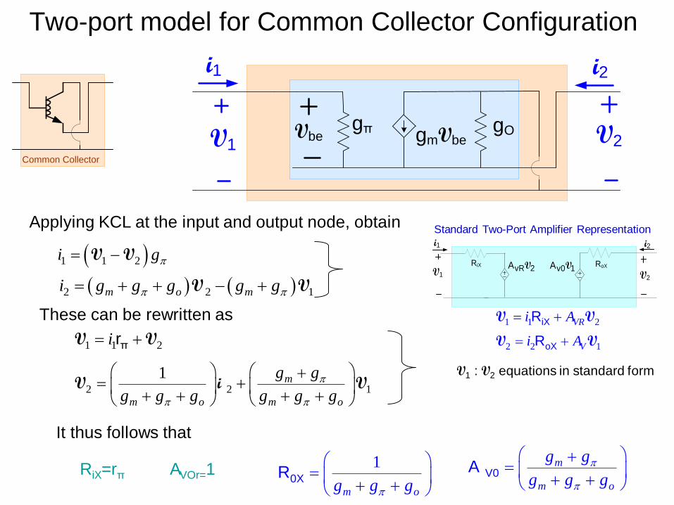
Two-port model for Common Collector Configuration
1 1 2i g V V
Common Collector
VbegOgmVbe
gπV1
i1
V2
i2
2 2 1m o mi g g g g g V V
Applying KCL at the input and output node, obtain
These can be rewritten as
1 1 2πri V V
2 2 1
1 m
m o m o
g g
g g g g g g
V i V
RiX=rπ AVOr=11
0XRm og g g
V0A m
m o
g g
g g g
It thus follows that
RoX
V1
i1
v0 1A VV2
RiX
i2
vR 2A V
V1 : V2 equations in standard form
1 1 2
2 2 1
iX
oX
R
R
VR
V
i A
i A
V V
V V
Standard Two-Port Amplifier Representation
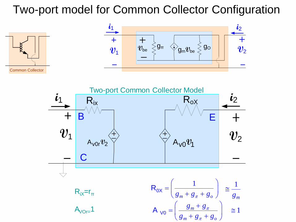
Two-port model for Common Collector Configuration
Common Collector
VbegOgmVbe
gπV1
i1
V2
i2
RiX=rπ
AVOr=1
10XR
m og g g
V0A m
m o
g g
g g g
RoX
V1v0 1A V
V2
Rixi2i1
v0r 2A V
B
C
E
Two-port Common Collector Model
1
mg
1
Common Collector Configuration
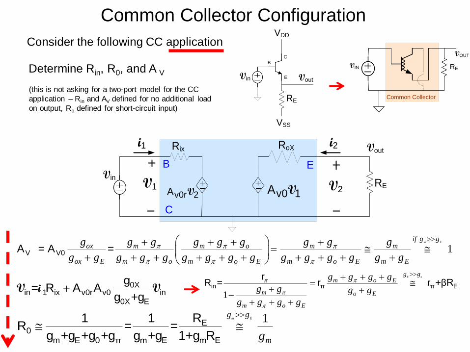
Consider the following CC application
B
E
C
VSS
VDD
Vin
RE
Vout
RoX
V1v0 1A V V2
Rixi2i1
v0r 2A V
VinRE
Vout
B
C
E
1V V0A = A =
m Eif g g
ox m m o m m
ox E m o m o E m o E m E
g g g g g g g g g
g g g g g g g g g g g g g g g
0X in 1 ix v0r v0 in
0X E
g= R A A
g +gV i V
1E0
m E 0 π m E m E
R1 1R = =
g +g +g +g g +g 1+g R
m E
g g
mg
Determine Rin, R0, and A V
(this is not asking for a two-port model for the CC
application – Rin and AV defined for no additional load
on output, Ro defined for short-circuit input)
1in π π E
rR = r r +βR
E og g
m o E
m o E
m o E
g g g g
g g g g
g g g g
Common Collector
REVIN
VOUT
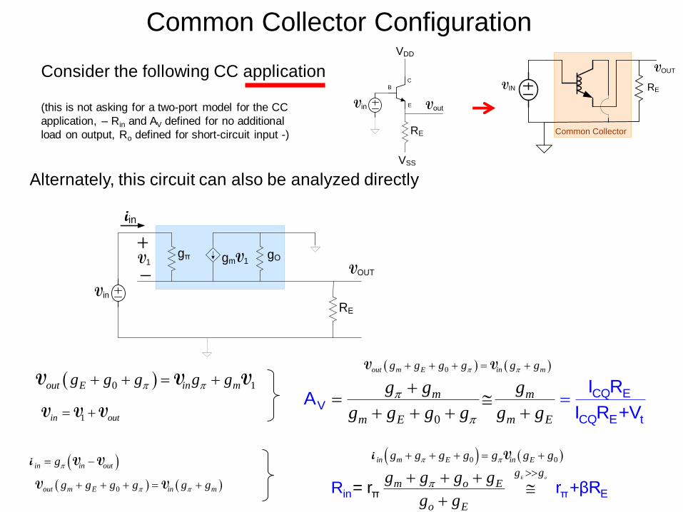
Common Collector Configuration
Consider the following CC applicationB
E
C
VSS
VDD
Vin
RE
Vout
Alternately, this circuit can also be analyzed directly
V1gOgmV1
gπ
RE
Vin
VOUT
iin
0 1out E in mg g g g g V V V
1in out V V V0
CQ EV
CQ E t
I RA
I R +V
m m
m E m E
g g g
g g g g g g
0out m E in mg g g g g g V V
0out m E in mg g g g g g V V
in in outg i V V 0 0in m E in Eg g g g g g g i V
in π EπR r += βR r
E og g
m o E
o E
g g g g
g g
(this is not asking for a two-port model for the CC
application, – Rin and AV defined for no additional
load on output, Ro defined for short-circuit input -) Common Collector
REVIN
VOUT
Common Collector Configuration
Consider the following CC applicationB
E
C
VSS
VDD
Vin
RE
Vout
V1gOgmV1
gπ
RE
Vin
VOUT
iin
0 out out E m outg g g gi V V
1 1out= R
E og g
m o E mg g g g g
(this is not asking for a two-port model for the CC
application, – Rin and AV defined for no additional
load on output, Ro defined for short-circuit input -) Common Collector
REVIN
VOUT
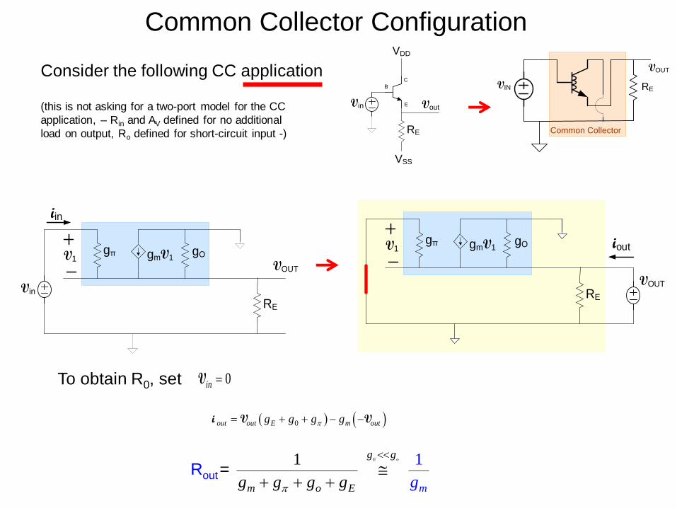
To obtain R0, set 0inV
V1gOgmV1
gπ
RE
VOUT
iout
Common Collector Configuration
Consider the following CC applicationB
E
C
VSS
VDD
Vin
RE
Vout
1 1out= R
E og g
m o E mg g g g g
(this is not asking for a two-port model for the CC
application, – Rin and AV defined for no additional
load on output, Ro defined for short-circuit input -)
0
1CQ EV
CQ E t
I RA
I R +V
m m
m E m E
g g g
g g g g g g
in π EπR r += βR r
E og g
m o E
o E
g g g g
g g
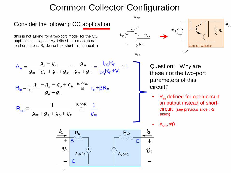
Question: Why are
these not the two-port
parameters of this
circuit?
RoX
V1v0 1A V
V2
Rixi2i1
v0r 2A V
B
C
E
Common Collector
REVIN
VOUT
• Rin defined for open-circuit
on output instead of short-
circuit (see previous slide : -2
slides)
• AV0r ≠0
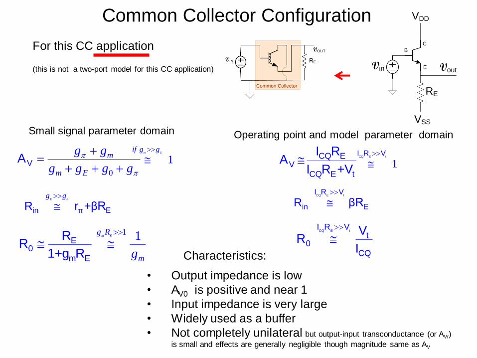
Common Collector Configuration
For this CC application B
E
C
VSS
VDD
Vin
RE
Vout
0
VA m
m E
g g
g g g g
in π ER r +βR
E o
g g
1 1E0
m E
RR
1+g R
m E
g R
mg
• Output impedance is low
• AV0 is positive and near 1
• Input impedance is very large
• Widely used as a buffer
• Not completely unilateral but output-input transconductance (or AVr)
is small and effects are generally negligible though magnitude same as AV
CQ EV
CQ E t
I RA
I R +V
CQ E tI R V
in ER βR
CQ E tI R V
t0
CQ
VR
I
(this is not a two-port model for this CC application)
1
m E
if g g
1CQ E tI R V
Common Collector
REVIN
VOUT
Small signal parameter domain Operating point and model parameter domain
Characteristics:
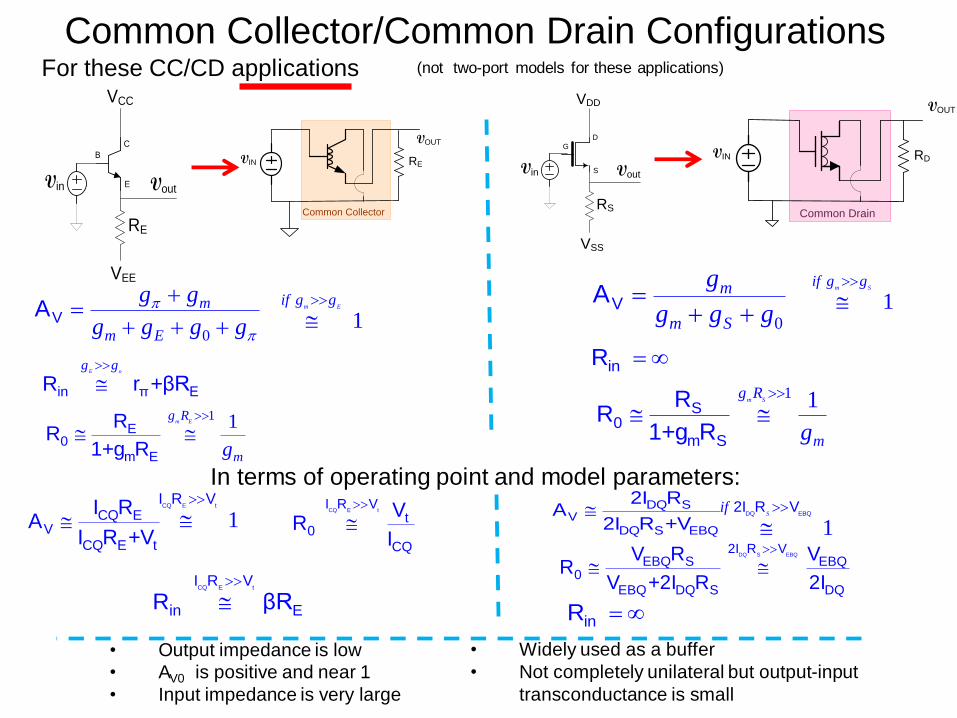
Common Collector/Common Drain ConfigurationsFor these CC/CD applications
B
E
C
VEE
VCC
Vin
RE
Vout
0
VA m
m E
g g
g g g g
in π ER r +βR
E o
g g
1 1E0
m E
RR
1+g R
m E
g R
mg
• Output impedance is low
• AV0 is positive and near 1
• Input impedance is very large
CQ EV
CQ E t
I RA
I R +V
CQ E tI R V
in ER βR
CQ E tI R V
t0
CQ
VR
I
(not two-port models for these applications)
1
m E
if g g
1CQ E tI R V
Common Collector
REVIN
VOUT
Common Drain
RDVIN
VOUT
G
S
D
VSS
Vin
RS
Vout
VDD
0
VA m
m S
g
g g g
1
m S
if g g
inR
1 1S0
m S
RR
1+g R
m S
g R
mg
In terms of operating point and model parameters:
• Widely used as a buffer
• Not completely unilateral but output-input
transconductance is small
DQ SV
DQ S EBQ
2I RA
2I R +V
1DQ EBQ
2I R V
S
if
DQ S EBQ2I R V
EBQ S EBQ0
EBQ DQ S DQ
V R VR
V +2I R 2I
inR
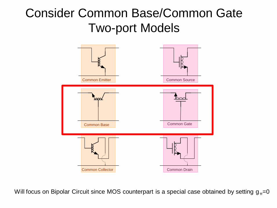
Consider Common Base/Common Gate
Two-port Models
Common Emitter
Common Base
Common Collector
Common Source
Common Gate
Common Drain
Will focus on Bipolar Circuit since MOS counterpart is a special case obtained by setting gπ=0
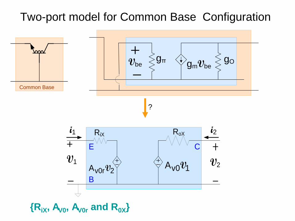
Two-port model for Common Base Configuration
?
VbegOgmVbe
gπ
Common Base
RoX
V1v0 1A V V2
RiXi2i1
v0r 2A V
B
E C
{RiX, AV0, AV0r and R0X}
Methods of Obtaining Amplifier Two-Port Network
1. VTEST : iTEST Method
2. Write V1 : V2 equations in standard form
3. Thevenin-Norton Transformations
4. Ad Hoc Approaches
Ro
V1
i1
v0 1A V V2
Rin
i2
vR 2A V
VR 2 1 1 IN
2 2 O V0 1
= R
= R +
A
A
+ V i V
V i V
Two-Port Models of Basic Amplifiers widely used for
Analysis and Design of Amplifier Circuits
Two-port model for Common Base Configuration
Common Base
1 1 1 2 0 1mg g g i V V V V
2 2 1 0 1mg g i V V V
From KCL
VbegOgmVbe
gπV1
i1
V2
i2
01 1 2
0 0
1
m m
g
g g g g g g
V i V
2 2 1
0 0
11 mg
g g
V i V
0
1 1iXR
m mg g g g
These can be rewritten as
It thus follows that:0
0
VOrAm
g
g g g
0 0
1V0A m mg g
g g 0
1oXR
g
V1 : V2 equations in standard form
VR 2 1 1 IN
2 2 O V0 1
= R
= R +
A
A
+ V i V
V i V
Standard Form for Amplifier Two-Port
Ro
V1
i1
v0 1A V V2
Rin
i2
vR 2A V
Two-port model for Common Base Configuration
Common Base
VbegOgmVbe
gπV1
i1
V2
i2
0
1 1iXR
m mg g g g
0 0
0
VOrA
m m
g g
g g g g
0 0
1V0A m mg g
g g
0
1oXR
g
RoX
v0 1A VV2
Rini2
v0r 2A V
B
E C
i1
V1
Two-port Common Base Model
Common Base Configuration
Consider the following CB application
B
E
C
VBB
VDD
Vin
RC
Vout
RoX
V1v0 1A V V2
RiXi2i1
v0r 2A V
B
E CVin
RC
Vout
0 0 0
0 0 0
CV V0
C 0X
RA = A
R +R
m mm
C
C
C
g g g g g
g g gg
gR
g
1 iX V0r out inin
1 1
R +AR = =
i VV
i i 0
0 0
1in
iX
V0r V
R=
1-A AR
C
C mm
g g
g g g g g g g
Cout
0 C
RR
1+g R
out C 0XR R //R
(this is not asking for a two-port model for this CB
application - – Rin and AV defined for no load on
output, Ro defined for short-circuit input ) VIN
Common Base
RC
VOUT
Common Base Configuration
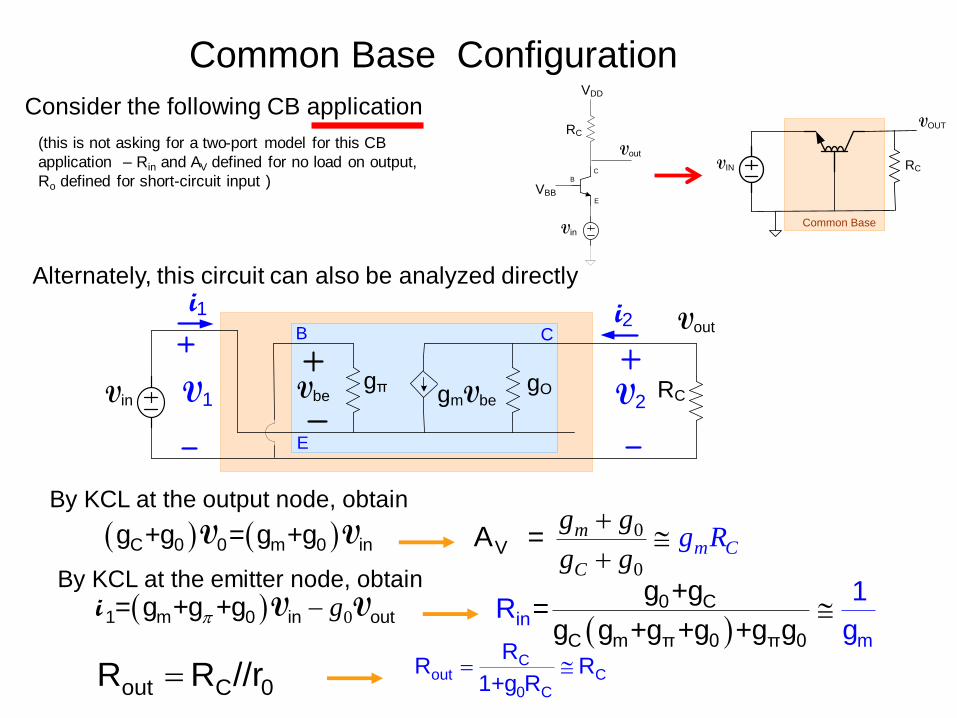
Consider the following CB application
B
E
C
VBB
VDD
Vin
RC
Vout
Cout C
0 C
RR R
1+g R
Alternately, this circuit can also be analyzed directly
VbegOgmVbe
gπV1
i1
V2
i2
RCVin
B
E
CVout
By KCL at the output node, obtain
C 0 0 m 0 ing +g = g +gV V 0
0
VA =
mm
C
C
g g
gg R
gBy KCL at the emitter node, obtain
01 m 0 in out= g +g +g g i V V
0 C
C m π 0 π 0in
m
g +g=
g g +g +g +g g
1R
g
out C 0R R //r
(this is not asking for a two-port model for this CB
application – Rin and AV defined for no load on output,
Ro defined for short-circuit input ) VIN
Common Base
RC
VOUT
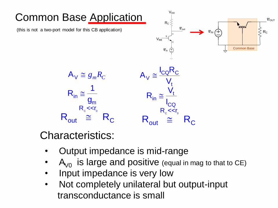
Common Base Application
B
E
C
VBB
VDD
Vin
RC
Vout
C 0R <<r
out CR R
VA m Cg R
inm
1R
g
CQ CV
t
I RA
V
tin
CQ
VR
I
C 0R <<r
out CR R
• Output impedance is mid-range
• AV0 is large and positive (equal in mag to that to CE)
• Input impedance is very low
• Not completely unilateral but output-input
transconductance is small
(this is not a two-port model for this CB application) VIN
Common Base
RC
VOUT
Characteristics:
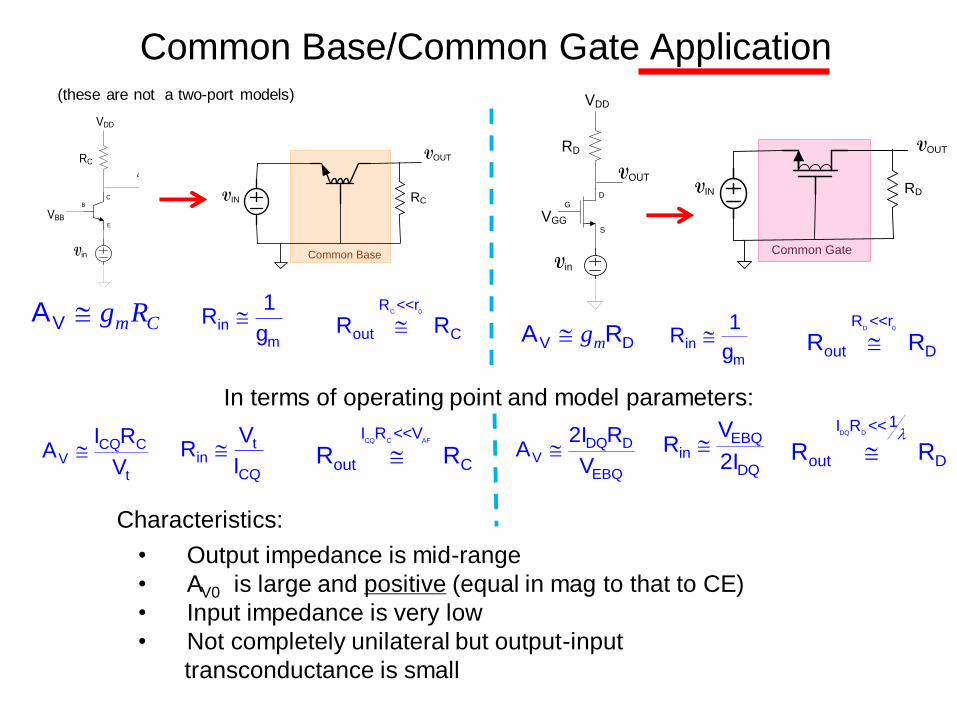
Common Base/Common Gate Application
B
E
C
VBB
VDD
Vin
RC
Vout
D 0R <<r
out DR RVA m Cg R
inm
1R
g
DQ DV
EBQ
2I RA
Vt
inCQ
VR
I
CQ C AFI R <<V
out CR R
• Output impedance is mid-range
• AV0 is large and positive (equal in mag to that to CE)
• Input impedance is very low
• Not completely unilateral but output-input
transconductance is small
(these are not a two-port models)
VIN
Common Base
RC
VOUT
In terms of operating point and model parameters:
Common Gate
VIN RD
VOUT
G
S
D
VGG
VDD
Vin
RD
VOUT
V DA R mg
C 0R <<r
out CR Rin
m
1R
g
CQ CV
t
I RA
V
EBQin
DQ
VR
2I
DQ D
1I R <<
out DR R
Characteristics:

End of Lecture 31