
EE 330 Lecture 23 - Iowa State University
51
EE 330 Lecture 23 •Thyristor Wrap-up •Area Comparison between MOS and Bipolar Circuits •Operating Point Characterization
Transcript of EE 330 Lecture 23 - Iowa State University

EE 330 Lecture 23
•Thyristor Wrap-up •Area Comparison between MOS and Bipolar Circuits •Operating Point Characterization

Bi-directional switching with the Triac
G
MT2
p
pn
n
n
MT1
nn
• Has two cross-coupled SCRs !
• Manufactured by diffusions
• Single Gate Control
MT1
MT2
G
Review from Last Lecture

The Basic Triac Circuit Assume ideal Triac
IT
VTR
IG=0
IH
BGF V
BGF -V
AC
L
VR
AC V
AC -V
AC
L
VR
−
CC T L TRV = I R +VLoad Line:
The solution of these two equations is at the intersection of the load line and the device characteristics
Analysis: AC T L TRV = I R +V
( ),FI TR GT1I = f V V
IT
VTR
IG=0
IH
BGF V
BGF -V
AC
L
VR
AC V
AC -V
AC
L
VR
−
Two stable operating points for both positive and negative VAC
VAC
VGT1
RL
VTRIT
Review from Last Lecture

IT
VTR
IG4>IG3>IG2>IG1=0
MT1
MT2
G
The Actual Triac Review from Last Lecture

MT1
MT2
G
IT
VM21
VGT1
IGIT
VM21
IG4>IG3>IG2>IG1=0
VM21
VGT1
Quadrant 1Quadrant 2
Quadrant 3 Quadrant 4
Quadrants of Operation Defined in VM21-VGT1 plane (not in the IT-VM21 plane)
But for any specific circuit, can map quadrants from the VM21-VGT1 plane to IT-VM21 plane

MT1
MT2
G
IT
VM21
VGT1
IG
VM21
VGT1
Quadrant 1Quadrant 2
Quadrant 3 Quadrant 4
Identification of Quadrants of Operation in IT -VM21 plane

MT1
MT2
G
IT
VM21
VGT1
IG
VM21
VGT1
Quadrant 1Quadrant 2
Quadrant 3 Quadrant 4
Identification of Quadrants of Operation in IT-VM21 plane
Curves may not be symmetric between Q1 and Q3 in the IT-VM21 plane Turn on current may be large and variable in Q4 (of the VM21-VGT1 )
Generally avoid operation in Q4 (of the VM21-VGT1 plane)
Most common to operate in Q2-Q3 quadrants or Q1-Q3 quadrants (of the VM21-VGT1 plane)

Some Basic Triac Application Circuits
VAC
RL
VTRIT
MT1
VGG
VAC
RL
VTRIT
MT1
VGG
VM21
VGT1
Quadrant 1Quadrant 2
Quadrant 3 Quadrant 4
Quad 1 : Quad 4
(not attractive because of Quad 4)
(VGG often from logic/control circuit) (VGG often from logic/control circuit)
Quad 2 : Quad 3

Some Basic Triac Application Circuits VAC
RL
VTRIT
MT1
VGG
VM21
VGT1
Quadrant 1Quadrant 2
Quadrant 3 Quadrant 4
Quad 2 : Quad 3
Limitations ?
If VAC is the standard 120VAC line voltage, where do we get the dc power supply?
120VAC
1K
10KVOUT
CFILTER
Direct digital control of trigger voltage/current with dedicated IC

Some Basic Triac Application Circuits
VAC
RL
VTRIT
MT1
VAC
RL
VTRIT
MT1
VAC
RL
VTRIT
MT1
Quad 1 : Quad 3
VM21
VGT1
Quadrant 1Quadrant 2
Quadrant 3 Quadrant 4
Quad 1 : Quad 3 Quad 1 : Quad 3

Some Basic Triac Application Circuits
VAC
RL
VTR
IT
MT1
VM21
VGT1
Quadrant 1Quadrant 2
Quadrant 3 Quadrant 4
Quad 1/ Quad 2 : Quad 3/Quad 4
Not real popular

Thyristor Types
• SCR • Triac • Bidirectional Phase-controlled thyristors (BCT) • LASCR (Light activated SCR) • Gate Turn-off thyristors (GTO) • FET-controlled thyristors(FET-CTH) • MOS Turn-off thyristors (MTO) • MOS-controlled thyristors (MCT)
Some of the more major types:

Thyristor Applications
Thyristors are available for working at very low current levels in electronic circuits to moderate current levels such is in incandescent light dimmers to very high current levels
ITRIAC from under 1mA to 10000A
Applications most prevalent for moderate to high current thyristors

SCR, rated about 100 amperes, 1200 volts, 1/2 inch stud, photographed by C J Cowie. Uploaded on 4 April 2006.

Thanks to Prof. Ajjarapu for providing the following slides:

From ABB Web Site
Diameter = 140mm

1988 Paper
Thanks to Prof. Ajjarapu for providing the following slides:

2008 Paper
Thanks to Prof. Ajjarapu for providing the following slides:

Thanks to Prof. Ajjarapu for providing the following slides:
Control Circuit
Thyristor

Stud- Mounted SCR 110 Amp RMS Rating
Stud Anode
Cathode Lead
Gate Lead (White)
Auxiliary Cathode Lead (Red) Extends cathode potential to the control circuit.
Thanks to Prof. Ajjarapu for providing the following slides:

Cross-section of a BCT wafer showing the antiparallel arrangement of the A and B component thyristors. The arrows indicate the convention of forward blocking for A and B.
Thanks to Prof. Ajjarapu for providing the following slides:

Thyristor Valve - 12 Pulse Converter ( 6.5Kv, 1568 Amp, Water cooled)
Thanks to Prof. Ajjarapu for providing the following slides:

Thyristor Observations
Many different structures used to build thyristors Range from low power devices to extremely high power devices Often single-wafer solutions for high power applications Usually formed by diffusions Widely used throughout society but little visibility Applications somewhat restricted

Thyristors
The good
SCRs Triacs
The bad Parasitic Device that can destroy integrated circuits

The Thyristor
S G D GS DConsider a Bulk-CMOS Process
A bipolar device in CMOS Processes
If this parasitic SCR turns on, either circuit will latch up or destroy itself
Guard rings must be included to prevent latchup Design rules generally include provisions for guard rings

MOS and Bipolar Area Comparisions
How does the area required to realize a MOSFET compare to that required to realize a BJT?
Will consider a minimum-sized device in both processes


1 5 10 15 20 25 30 35 40 45 50 60 55 70 65 75 1
5
10
20
15
30
25
40
35
50
45
55
Consider Initially the Emitter in the BJT surrounded by a base region


1 5 10 15 20 25 30 35 40 45 50 60 55 70 65 75 1
5
10
20
15
30
25
40
35
50
45
55
From design rules (left to right) 4.3, 5.1, 5.4, 5.6, 5.5
3λ
4λ
2λ2λ
2λ
19λ
12λ

1 5 10 15 20 25 30 35 40 45 50 60 55 70 65 75 1
5
10
20
15
30
25
40
35
50
45
55
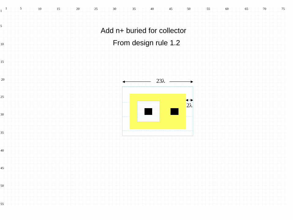
23λ
2λ
Add n+ buried for collector
From design rule 1.2


1 5 10 15 20 25 30 35 40 45 50 60 55 70 65 75 1
5
10
20
15
30
25
40
35
50
45
55
23λ
14λ 14λ
51λ
14λ 14λ
Add n-epi region from design rules 2.3 and 3.3

1 5 10 15 20 25 30 35 40 45 50 60 55 70 65 75 1
5
10
20
15
30
25
40
35
50
45
55
3λ 2λ
23λ
14λ
51λ
14λ
4λ
Add contact to n-epi region from design rules 2.3 and 3.3


1 5 10 15 20 25 30 35 40 45 50 60 55 70 65 75 1
5
10
20
15
30
25
40
35
50
45
55
14λ
61λ
14λ
4λ 6λ
12λ
2λ 2λ
NOT TO SCALE
Note: 26λ required Between p-base and isolation diffusion
19λ
But, there are some rather strict rules relating to the epi contact
from (left to right) rules 4.4, 5.4, 4.6

1 5 10 15 20 25 30 35 40 45 50 60 55 70 65 75 1
5
10
20
15
30
25
40
35
50
45
55
26λ
71λ
6λ
12λ
2λ
2λ
Note: 26λ required Between p-base and isolation diffusion
Note: Not to vertical Scale
44λ
19λ
14λ
Consider a structure with a collector contact on both sides of epi

1 5 10 15 20 25 30 35 40 45 50 60 55 70 65 75 1
5
10
20
15
30
25
40
35
50
45
55
26λ
71λ
6λ
12λ
2λ
Note: 26λ required Between p-base and isolation diffusion
Note: Not to vertical Scale
44λ
4λ
19λ
26λ

1 5 10 15 20 25 30 35 40 45 50 60 55 70 65 75 1
5
10
20
15
30
25
40
35
50
45
55
71λ
Note: Not to vertical Scale
44λ
75λ
48λ
1 5 10 15 20 25 30 35 40 45 50 60 55 70 65 75 1
5
10
20
15
30
25
40
35
50
45
55
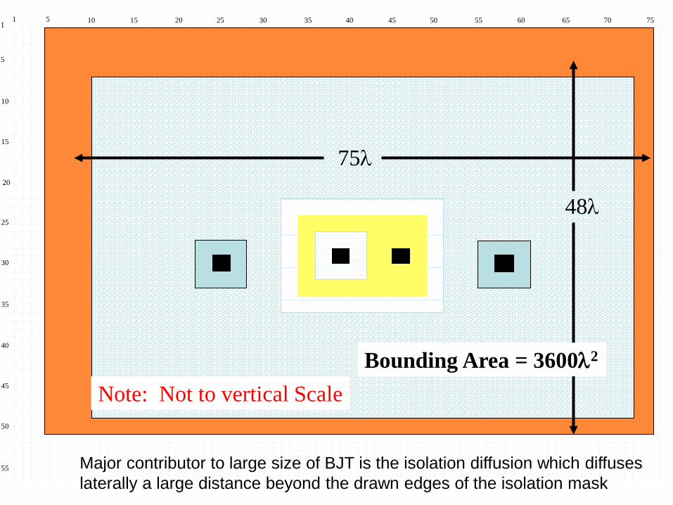
Note: Not to vertical Scale
75λ
48λ
Bounding Area = 3600λ2
Major contributor to large size of BJT is the isolation diffusion which diffuses laterally a large distance beyond the drawn edges of the isolation mask

1 5 10 15 20 25 30 35 40 45 50 60 55 70 65 75 1
5
10
20
15
30
25
40
35
50
45
55
16λ
13λ
Bounding Area = 208λ2
Comparison with Area for n-channel MOSFET in Bulk CMOS

1 5 10 15 20 25 30 35 40 45 50 60 55 70 65 75 1
5
10
20
15
30
25
40
35
50
45
55
14λ
12λ
Bounding Area = 168λ2
Active Area = 6λ2
Minimum-Sized MOSFET

1 5 10 15 20 25 30 35 40 45 50 60 55 70 65 75 1
5
10
20
15
30
25
40
35
50
45
55 Note: Not to vertical Scale
75λ
48λ
MOSFET BJT

Area Comparison between BJT and MOSFET
• BJT Area = 3600 λ2
• n-channel MOSFET Area = 168 λ2 • Area Ratio = 21:1

Operating Point of Electronic Circuits Often interested in circuits where a small signal input is to be amplified The electrical port variables where the small signal goes to 0 is termed the Operating Point, the Bias Point, the Quiescent Point, or simply the Q-Point By setting the small signal to 0, it means replacing small voltage inputs with short circuits and small current inputs with open circuits When analyzing small-signal amplifiers, it is necessary to obtain the Q-point When designing small-signal amplifiers, establishing of the desired Q-point is termed “biasing” Capacitors become open circuits (and inductors short circuits) when determining Q-points Simplified dc models of the MOSFET (saturation region) or BJT (forward active region) are usually adequate for determining the Q-point in practical amplifier circuits

End of Lecture 23