
EE 330 Lecture 16 Devices in Semiconductor Processes
40
EE 330 Lecture 16 Devices in Semiconductor Processes • Capacitors • MOSFETs
Transcript of EE 330 Lecture 16 Devices in Semiconductor Processes
EE 330Lecture 16
Devices in Semiconductor Processes
• Capacitors
• MOSFETs
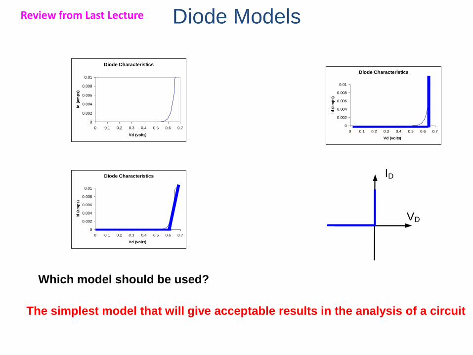
Diode Models
ID
VD
Diode Characteristics
0
0.002
0.004
0.006
0.008
0.01
0 0.1 0.2 0.3 0.4 0.5 0.6 0.7
Vd (volts)
Id (
am
ps)
Diode Characteristics
0
0.002
0.004
0.006
0.008
0.01
0 0.1 0.2 0.3 0.4 0.5 0.6 0.7
Vd (volts)
Id (
am
ps)
Diode Characteristics
0
0.002
0.004
0.006
0.008
0.01
0 0.1 0.2 0.3 0.4 0.5 0.6 0.7
Vd (volts)
Id (
am
ps)
Which model should be used?
The simplest model that will give acceptable results in the analysis of a circuit
Review from Last Lecture

Use of Piecewise Models for Nonlinear Devices
when Analyzing Electronic Circuits
Process:
1. Guess state of the device
2. Analyze circuit
3. Verify State
4. Repeat steps 1 to 3 if verification fails5. Verify model (if necessary)
Observations:
o Analysis generally simplified dramatically (particularly if piecewise model is linear)
o Approach applicable to wide variety of nonlinear deviceso Closed-form solutions give insight into performance of circuito Usually much faster than solving the nonlinear circuit directlyo Wrong guesses in the state of the device do not compromise solution
(verification will fail)
o Helps to guess right the first timeo Detailed model is often not necessary with most nonlinear deviceso Particularly useful if piecewise model is PWL (but not necessary)
o For practical circuits, the simplified approach usually applies
Key Concept For Analyzing Circuits with Nonlinear Devices
Rev
iew
fro
m L
ast
Lect
ure
0.00E+00
5.00E-03
1.00E-02
1.50E-02
2.00E-02
2.50E-02
3.00E-02
3.50E-02
4.00E-02
4.50E-02
5.00E-02
0 0.2 0.4 0.6 0.8
ID
VDVBR
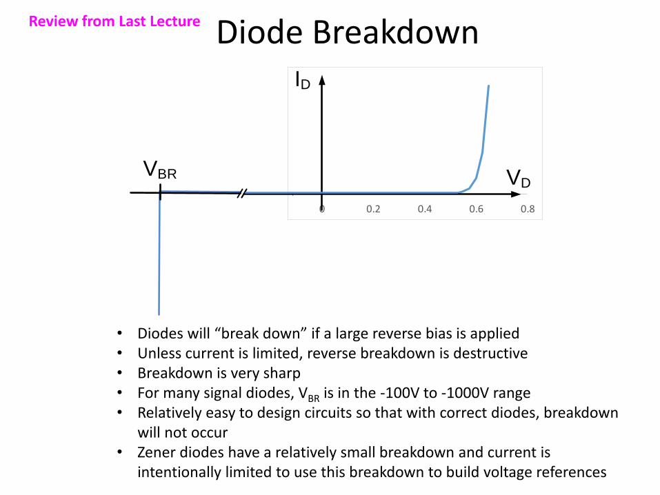
Diode Breakdown
• Diodes will “break down” if a large reverse bias is applied• Unless current is limited, reverse breakdown is destructive• Breakdown is very sharp• For many signal diodes, VBR is in the -100V to -1000V range• Relatively easy to design circuits so that with correct diodes, breakdown
will not occur• Zener diodes have a relatively small breakdown and current is
intentionally limited to use this breakdown to build voltage references
Review from Last Lecture
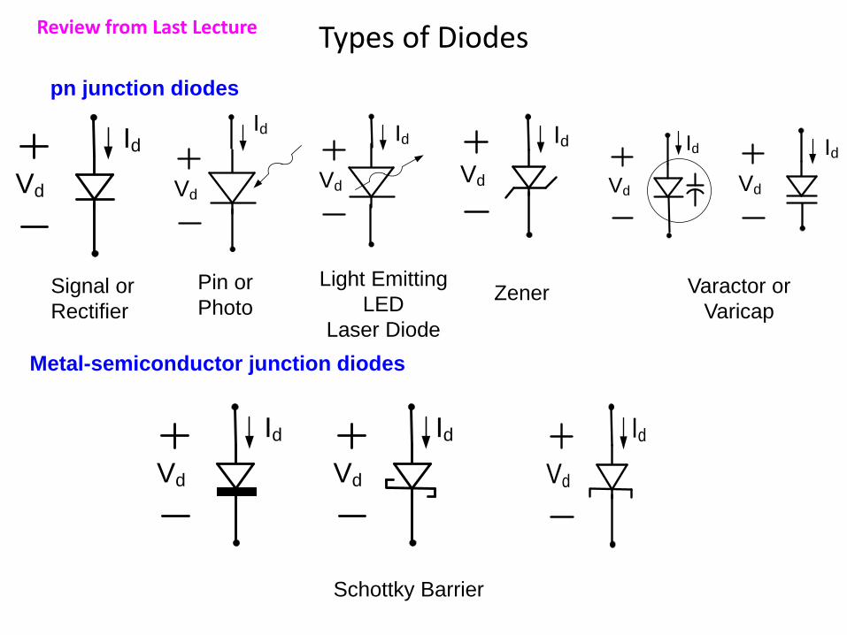
Types of Diodes
Vd
Id Id
Vd
Id
VdVd
Id
Vd
Id
Vd
Id
Vd
Id
Vd
Id
pn junction diodes
Metal-semiconductor junction diodes
Signal or
Rectifier
Pin or
Photo
Light Emitting
LED
Laser Diode
Zener Varactor or
Varicap
Schottky Barrier
Vd
Id
Review from Last Lecture
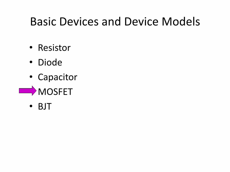
Basic Devices and Device Models
• Resistor
• Diode
• Capacitor
• MOSFET
• BJT
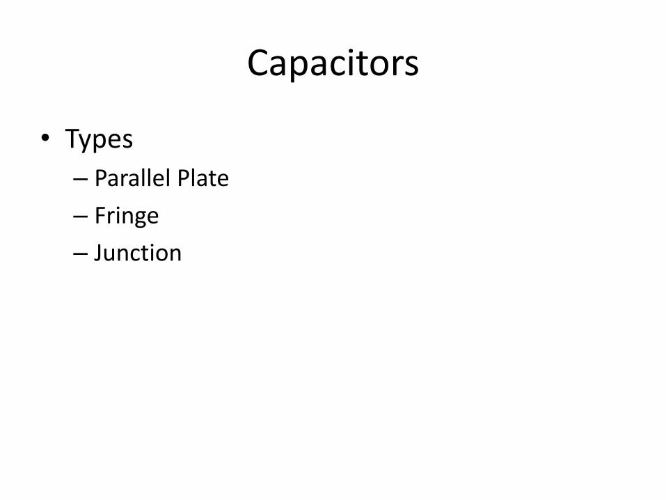
Capacitors
• Types
– Parallel Plate
– Fringe
– Junction
Parallel Plate Capacitors
C
d
A1
A2
cond1
cond2
insulator
A = area of intersection of A1 & A2
d
AC
One (top) plate intentionally sized smaller to determine C
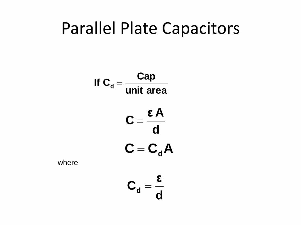
Parallel Plate Capacitors
ACC d
d
AεC
areaunit
CapC If d
d
εCd
where
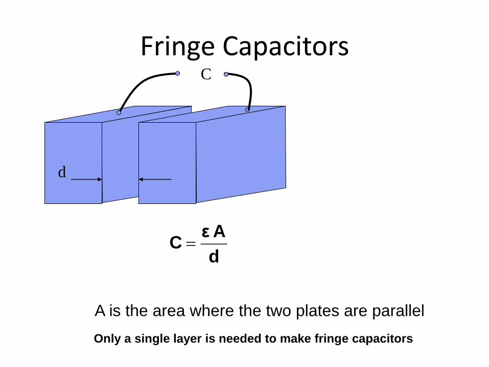
Fringe Capacitors
d
C
d
AεC
A is the area where the two plates are parallel
Only a single layer is needed to make fringe capacitors
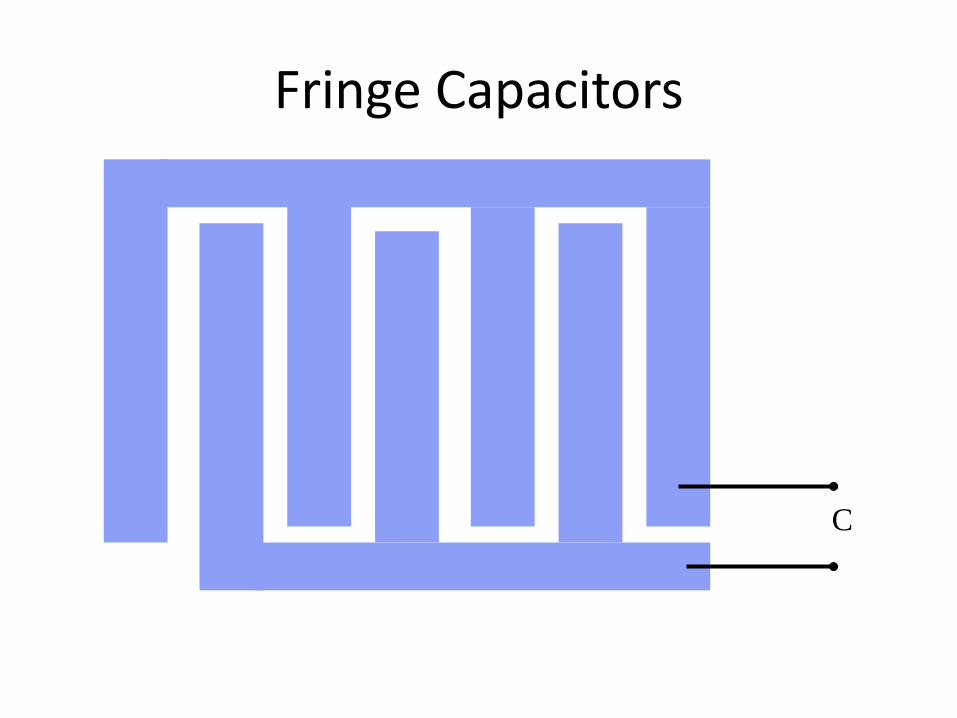
Fringe Capacitors
C
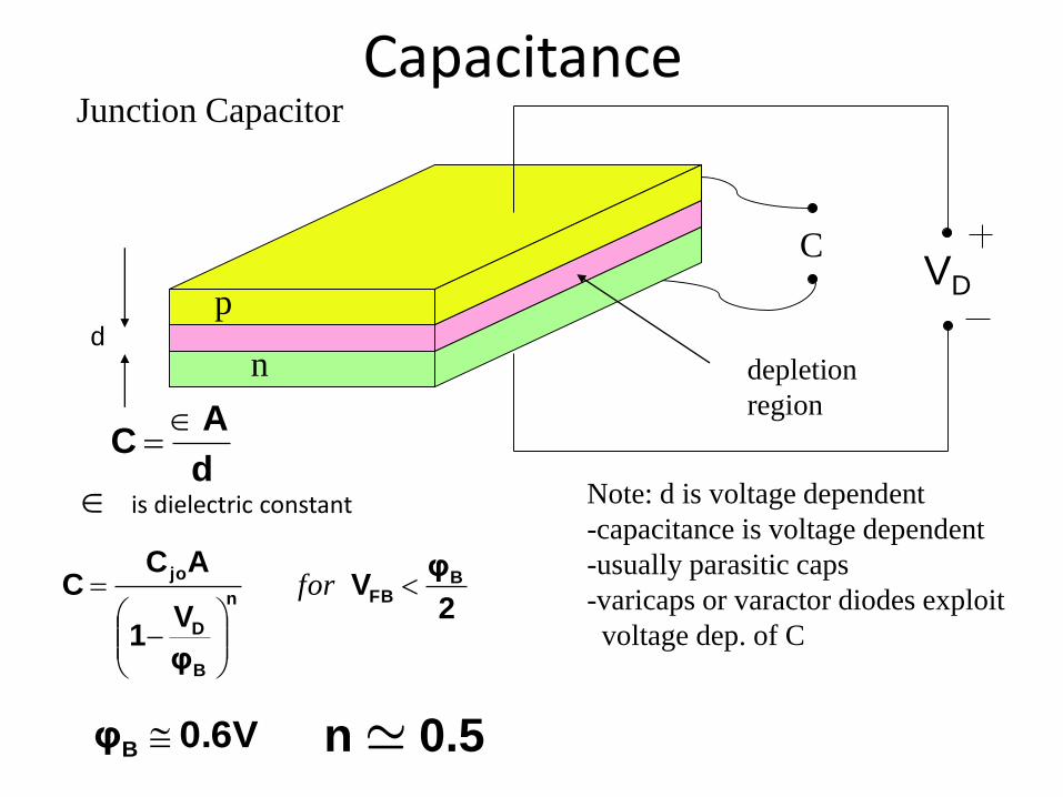
Capacitance
2
φV
φ
V1
ACC B
FBn
B
D
jo
for
ddepletion
region
C
Junction Capacitor
d
AC
Note: d is voltage dependent
-capacitance is voltage dependent
-usually parasitic caps
-varicaps or varactor diodes exploit
voltage dep. of C
d
p
n
VD
0.6VφB n ; 0.5
is dielectric constant
Capacitance
2
φV
φ
V1
ACC B
FBn
B
D
jo
for
Junction Capacitor
0.6VφB n ; 0.5
0
0.2
0.4
0.6
0.8
1
1.2
1.4
1.6
-4 -3 -2 -1 0 1
j0
C
C A
VD
Voltage dependence is substantial
VD
Basic Devices and Device Models
• Resistor
• Diode
• Capacitor
• MOSFET
• BJT
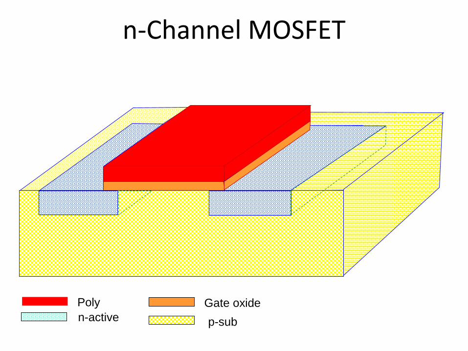
n-Channel MOSFET
Poly
n-active
Gate oxide
p-sub
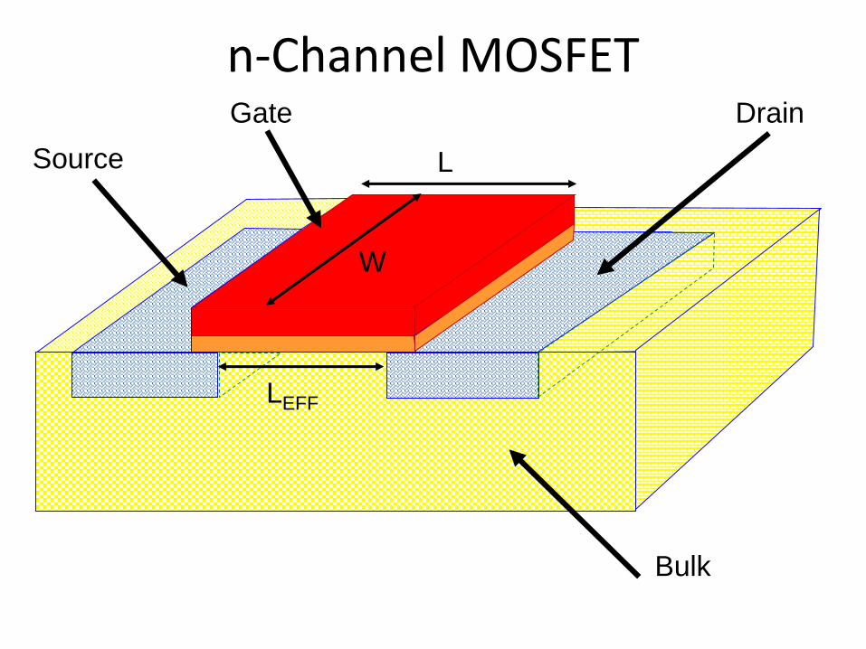
n-Channel MOSFET
LEFF
L
W
Source
DrainGate
Bulk
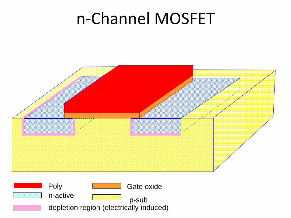
n-Channel MOSFET
Poly
n-active
Gate oxide
p-subdepletion region (electrically induced)
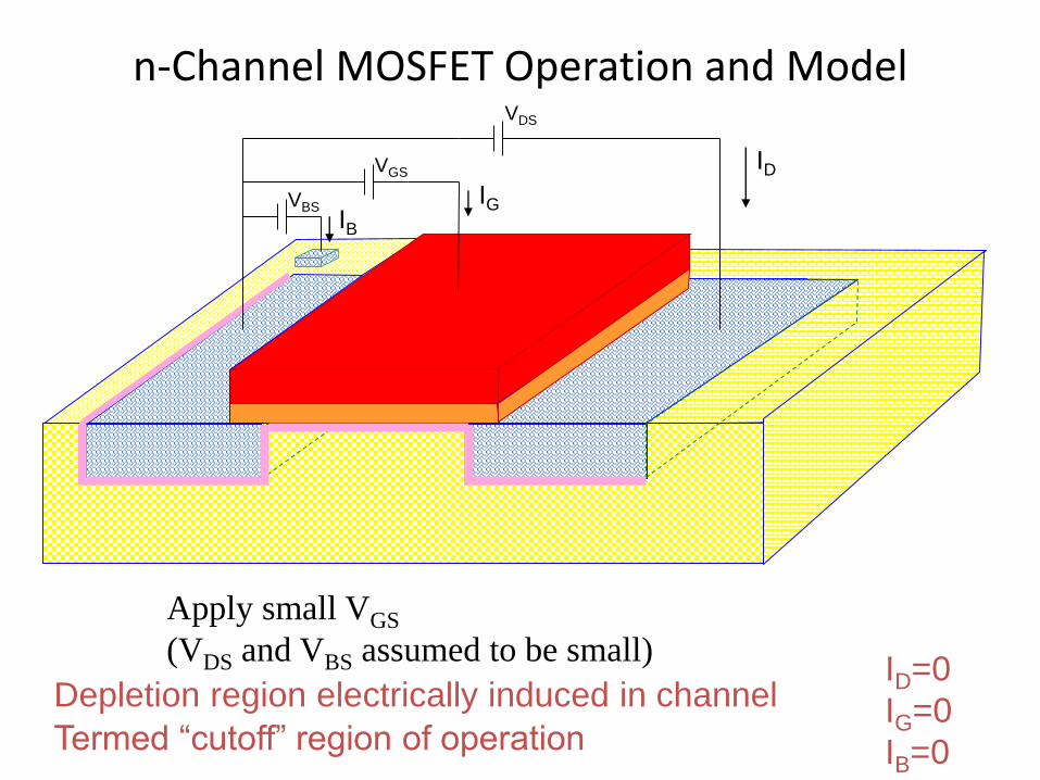
n-Channel MOSFET Operation and Model
VBS
VGS
VDS
Apply small VGS
(VDS and VBS assumed to be small)ID=0
IG=0
IB=0
Depletion region electrically induced in channel
IDIG
IB
Termed “cutoff” region of operation
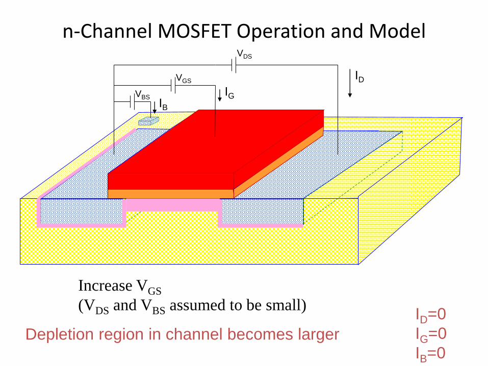
n-Channel MOSFET Operation and Model
VBS
VGS
VDS
Increase VGS
(VDS and VBS assumed to be small)ID=0
IG=0
IB=0Depletion region in channel becomes larger
IDIG
IB

n-Channel MOSFET Operation and Model
VBS
VGS
VDS
ID=0
IG=0
IB=0
IDIG
IB
Model in Cutoff Region
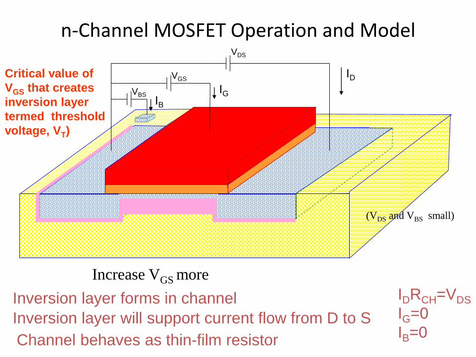
n-Channel MOSFET Operation and Model
VBS
VGS
VDS
Increase VGS more
IDRCH=VDS
IG=0
IB=0
Inversion layer forms in channel
IDIG
IB
(VDS and VBS small)
Inversion layer will support current flow from D to S
Channel behaves as thin-film resistor
Critical value of
VGS that creates
inversion layer
termed threshold
voltage, VT)
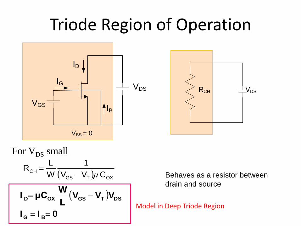
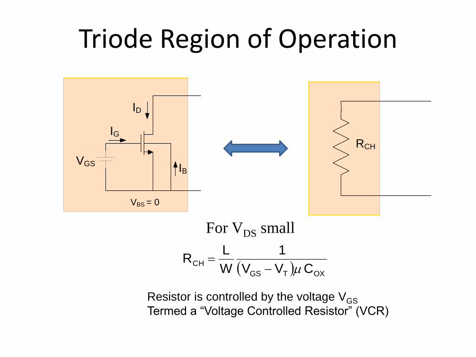
Triode Region of Operation
OXTGS
CHCVV
1
W
LR
0II
VVVL
WμCI
BG
DSTGSOXD
For VDS small
VDS
VBS = 0
VGS
ID
IG
IB
VDSRCH
Behaves as a resistor between
drain and source
Model in Deep Triode Region
Triode Region of Operation
OXTGS
CHCVV
1
W
LR
For VDS small
VBS = 0
VGS
ID
IG
IB
RCH
Resistor is controlled by the voltage VGS
Termed a “Voltage Controlled Resistor” (VCR)
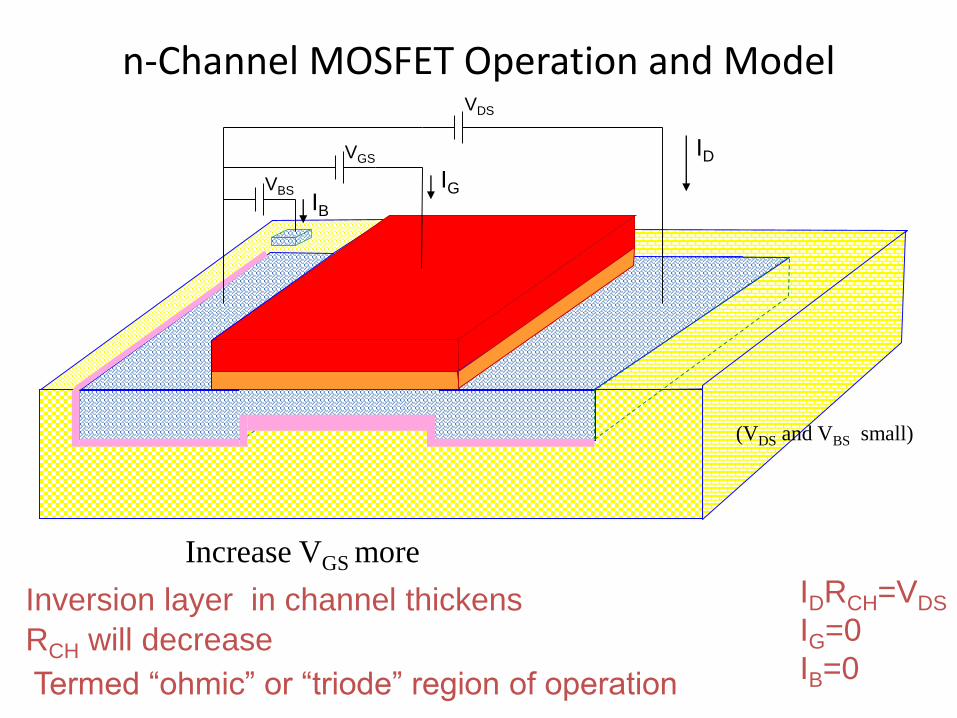
n-Channel MOSFET Operation and Model
VBS
VGS
VDS
Increase VGS more
IDRCH=VDS
IG=0
IB=0
Inversion layer in channel thickens
IDIG
IB
(VDS and VBS small)
RCH will decrease
Termed “ohmic” or “triode” region of operation
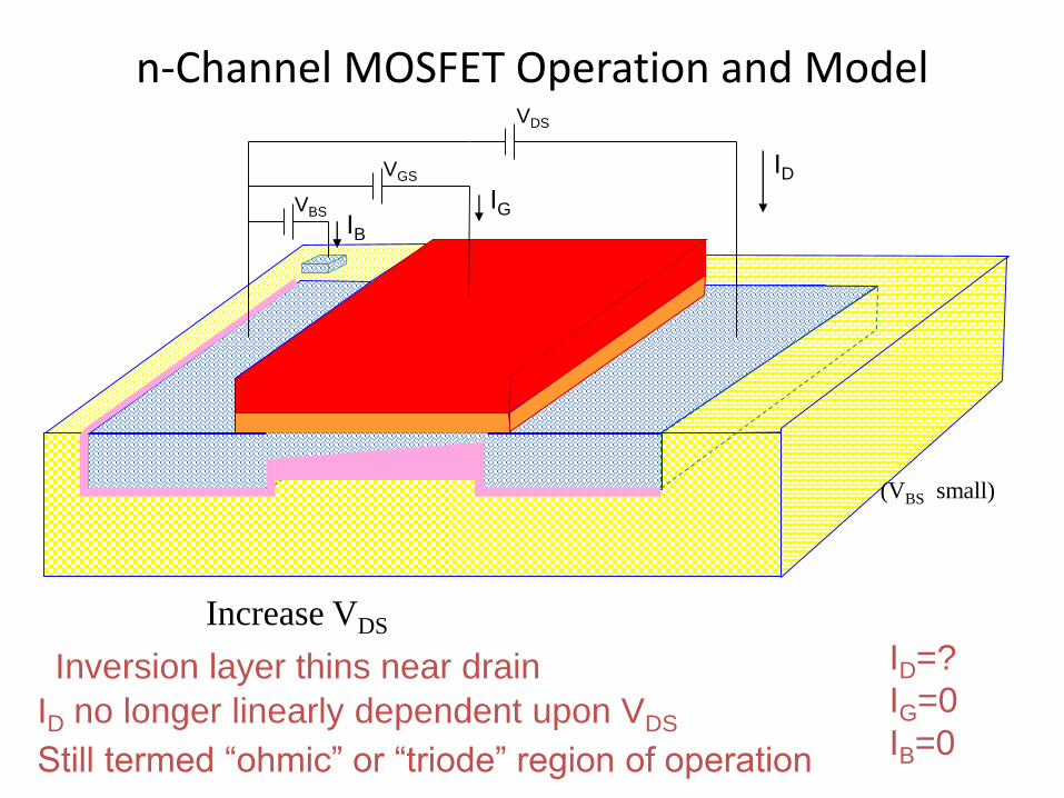
n-Channel MOSFET Operation and Model
VBS
VGS
VDS
Increase VDS
ID=?
IG=0
IB=0
Inversion layer thins near drain
IDIG
IB
(VBS small)
ID no longer linearly dependent upon VDS
Still termed “ohmic” or “triode” region of operation
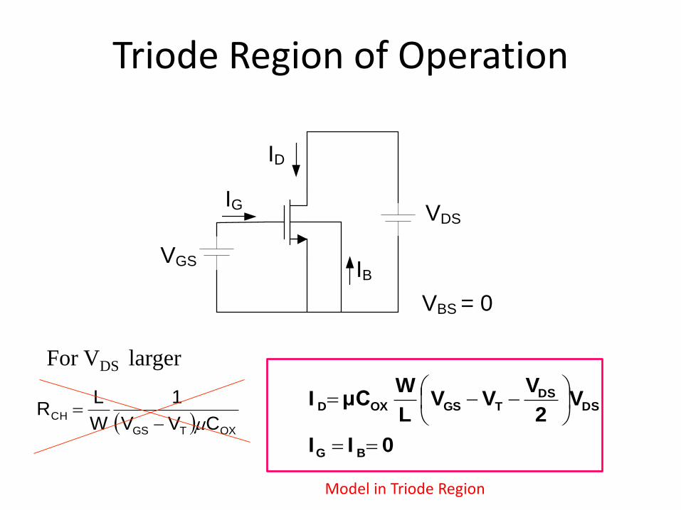
Triode Region of Operation
VDS
VBS = 0
VGS
ID
IG
IB
OXTGS
CHCVV
1
W
LR
0II
V2
VVV
L
WμCI
BG
DSDS
TGSOXD
For VDS larger
Model in Triode Region
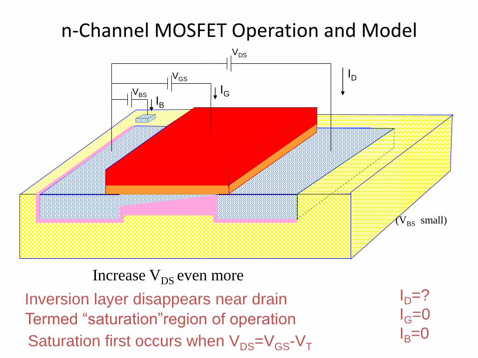
n-Channel MOSFET Operation and Model
VBS
VGS
VDS
Increase VDS even more
ID=?
IG=0
IB=0
Inversion layer disappears near drain
IDIG
IB
(VBS small)
Termed “saturation”region of operation
Saturation first occurs when VDS=VGS-VT
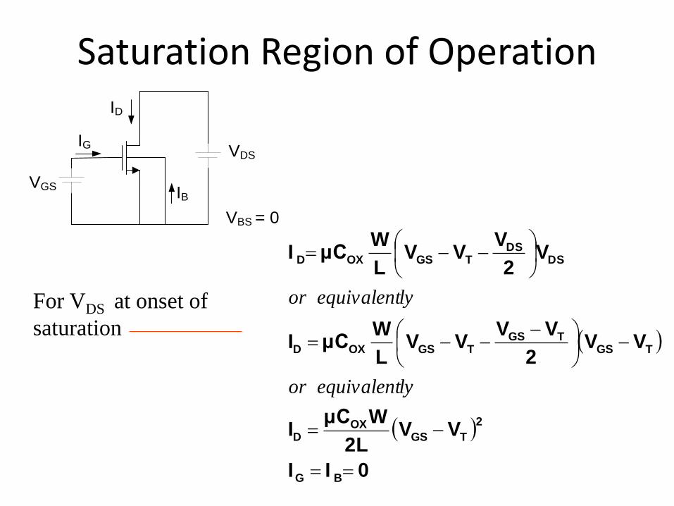
Saturation Region of Operation
VDS
VBS = 0
VGS
ID
IG
IB
0II
VV2L
WμCI
VV2
VVVV
L
WμCI
V2
VVV
L
WμCI
BG
2
TGSOX
D
TGSTGS
TGSOXD
DSDS
TGSOXD
lyequivalentor
lyequivalentorFor VDS at onset of
saturation
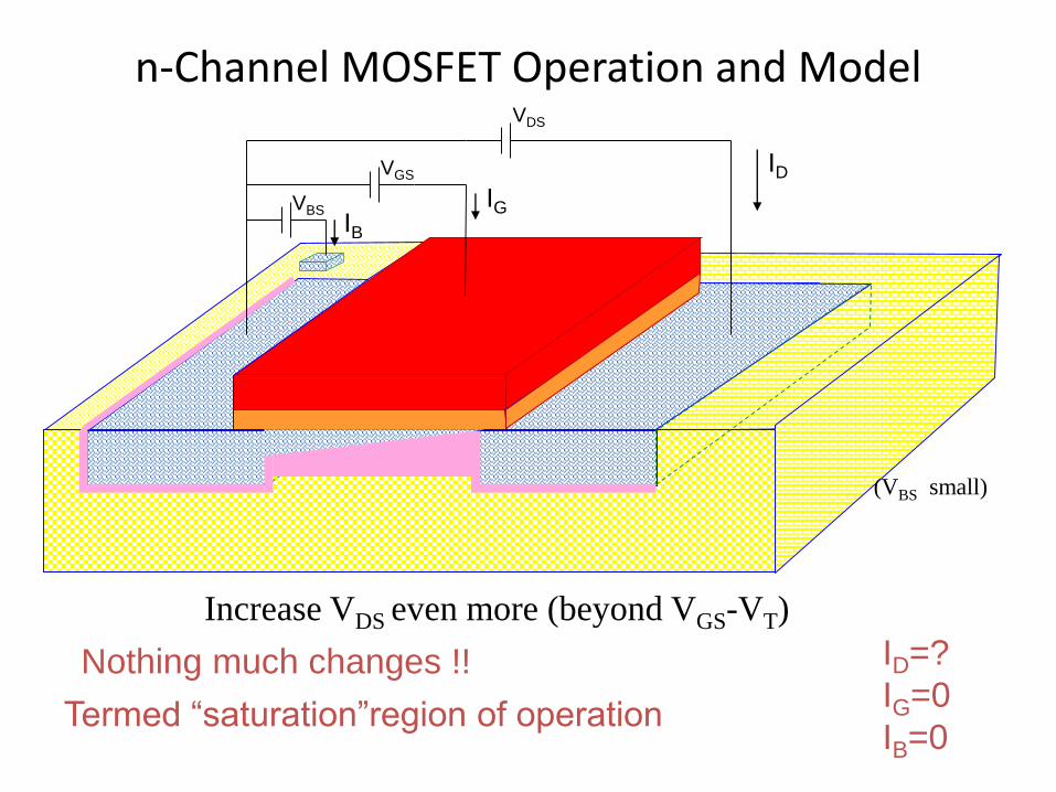
n-Channel MOSFET Operation and Model
VBS
VGS
VDS
Increase VDS even more (beyond VGS-VT)
ID=?
IG=0
IB=0
Nothing much changes !!
IDIG
IB
(VBS small)
Termed “saturation”region of operation
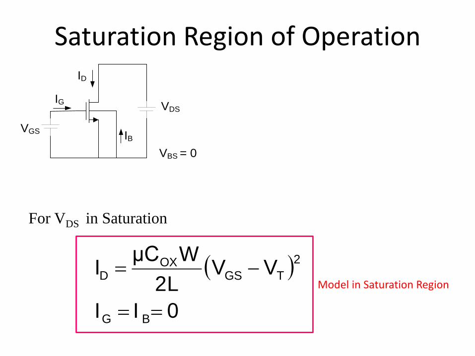
Saturation Region of Operation
VDS
VBS = 0
VGS
ID
IG
IB
0II
VV2L
WμCI
BG
2
TGSOX
D
For VDS in Saturation
Model in Saturation Region
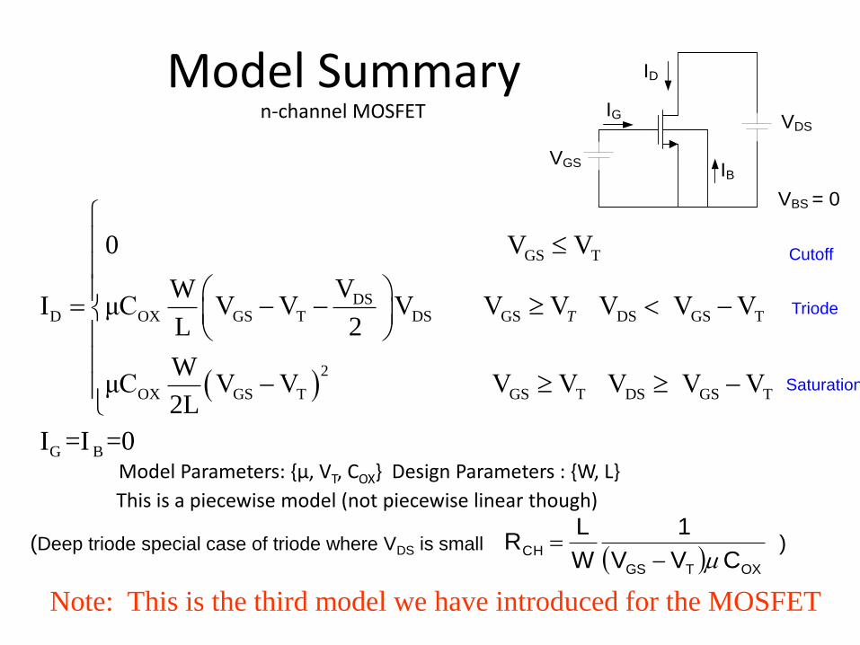
Model SummaryVDS
VBS = 0
VGS
ID
IG
IB
GS T
DSD OX GS T DS GS DS GS T
2
OX GS T GS T DS GS T
G B
0 V V
VWI μC V V V V V V V V
L 2
WμC V V V V V V V
2L
I =I =0
T
Note: This is the third model we have introduced for the MOSFET
Cutoff
Triode
Saturation
OXTGS
CHCVV
1
W
LR
(Deep triode special case of triode where VDS is small )
This is a piecewise model (not piecewise linear though)
n-channel MOSFET
Model Parameters: {µ, VT, COX} Design Parameters : {W, L}
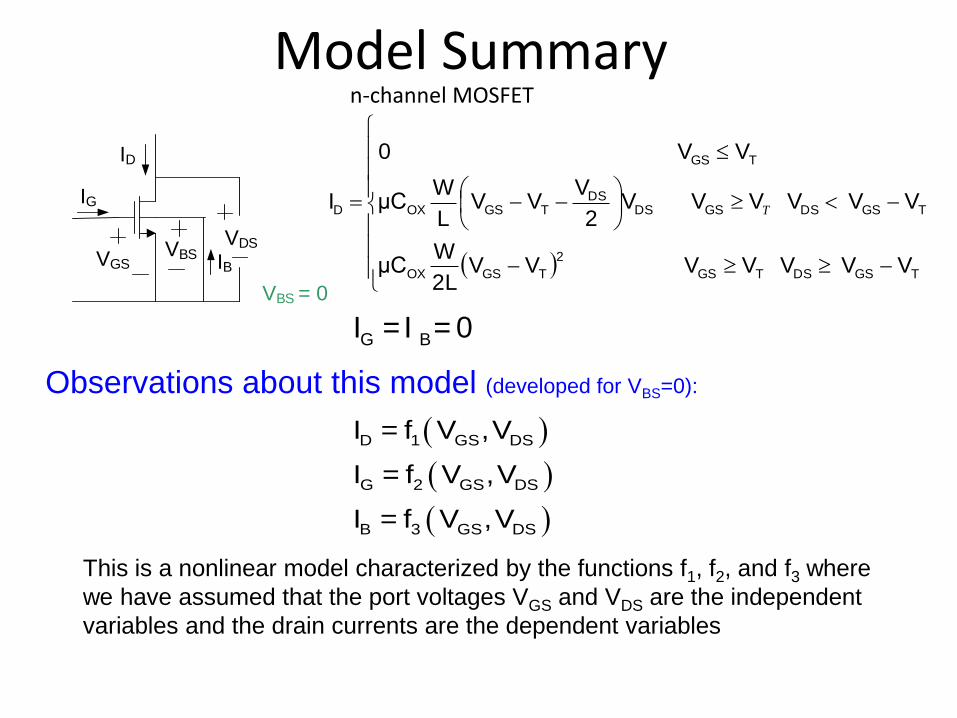
Model Summary
VDS
VBS = 0
VGS
ID
IG
IBVBS
TGSDSTGS
2
TGSOX
TGSDSGSDSDS
TGSOX
TGS
D
VVVVVVV2L
WμC
VVVVVV2
VVV
L
WμC
VV0
I T
Observations about this model (developed for VBS=0):
D 1 GS DS
G 2 GS DS
B 3 GS DS
I = f V ,V
I = f V ,V
I = f V ,V
This is a nonlinear model characterized by the functions f1, f2, and f3 where
we have assumed that the port voltages VGS and VDS are the independent
variables and the drain currents are the dependent variables
G BI = I = 0
n-channel MOSFET
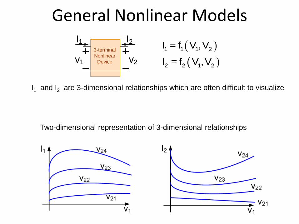
General Nonlinear Models
1 1 1 2
2 2 1 2
I = f V ,V
I = f V ,V
I1 and I2 are 3-dimensional relationships which are often difficult to visualize
v1 v2
I1 I23-terminal
Nonlinear
Device
Two-dimensional representation of 3-dimensional relationships
Graphical Representation of MOS Model
G BI =I =0
0
0.5
1
1.5
2
2.5
3
0 1 2 3 4 5
VDS
Cutoff
Triode
Saturation
ID
VDS
VGS1
VGS2
VGS3
VGS4
Deep Triode
RegionRegion
2
DSD OX
VWI =μC
L 2
Parabola separated triode and saturation regions and corresponds to VDS=VGS-VT
GS T
DS
D OX GS T DS GS DS GS T
2
OX GS T GS T DS GS T
0 V V
VWI μC V V V V V V V V
L 2
WμC V V V V V V V
2L
T
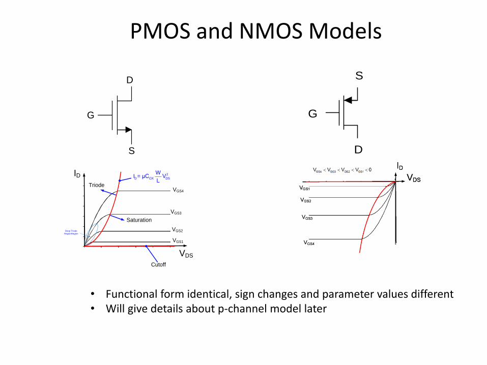
PMOS and NMOS Models
S
D
G
0
0.5
1
1.5
2
2.5
3
0 1 2 3 4 5
VDS
Cutoff
Triode
Saturation
ID
VDS
2
D OX DS
WI = μC V
L
VGS1
VGS2
VGS3
VGS4
Deep Triode
RegionRegion
D
S
G
• Functional form identical, sign changes and parameter values different• Will give details about p-channel model later
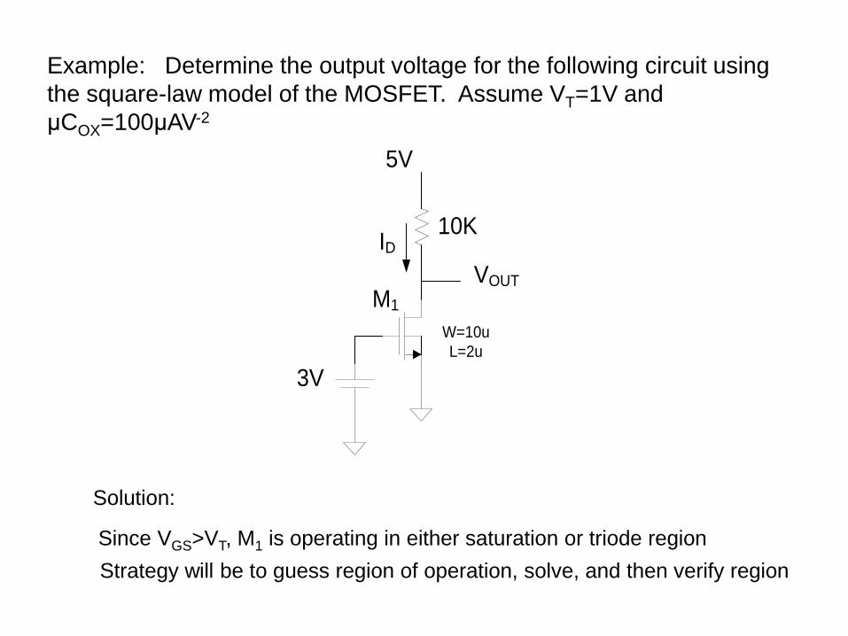
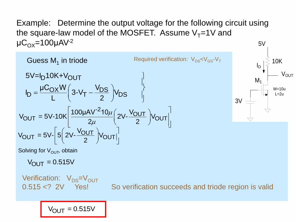
Example: Determine the output voltage for the following circuit using
the square-law model of the MOSFET. Assume VT=1V and
μCOX=100μAV-2
Solution:
Since VGS>VT, M1 is operating in either saturation or triode region
10K
W=10u
L=2u
5V
3V
VOUT
M1
ID
Strategy will be to guess region of operation, solve, and then verify region
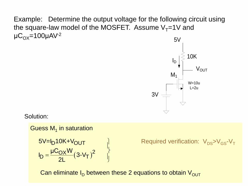
Example: Determine the output voltage for the following circuit using
the square-law model of the MOSFET. Assume VT=1V and
μCOX=100μAV-2
Solution:
10K
W=10u
L=2u
5V
3V
VOUT
M1
ID
Guess M1 in saturation
D OUT
2OXD T
5V=I 10K+V
μC WI 3-V
2L
Required verification: VDS>VGS-VT
Can eliminate ID between these 2 equations to obtain VOUT
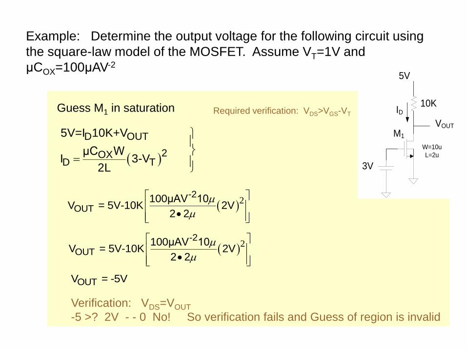
Example: Determine the output voltage for the following circuit using
the square-law model of the MOSFET. Assume VT=1V and
μCOX=100μAV-2
10K
W=10u
L=2u
5V
3V
VOUT
M1
IDGuess M1 in saturation
D OUT
2OXD T
5V=I 10K+V
μC WI 3-V
2L
Required verification: VDS>VGS-VT
2-2
OUT100μAV 10
V = 5V-10K 2V2 2
2-2
OUT100μAV 10
V = 5V-10K 2V2 2
OUTV = -5V
Verification: VDS=VOUT
-5 >? 2V - - 0 No! So verification fails and Guess of region is invalid
Example: Determine the output voltage for the following circuit using
the square-law model of the MOSFET. Assume VT=1V and
μCOX=100μAV-2
10K
W=10u
L=2u
5V
3V
VOUT
M1
IDGuess M1 in triode
D OUT
OX DSD T DS
5V=I 10K+V
μC W VI 3-V V
L 2
Required verification: VDS<VGS-VT
-2OUT
OUT OUTV100μAV 10
V = 5V-10K 2V- V2 2
OUTV = 0.515V
Verification: VDS=VOUT
0.515 <? 2V Yes! So verification succeeds and triode region is valid
OUTOUT OUT
VV = 5V- 5 2V- V
2
Solving for VOUT, obtain
OUTV = 0.515V

End of Lecture 16


![EE 330 Lecture 42 - Iowa State Universityclass.ece.iastate.edu/ee330/lectures/EE 330 Lect 42 Fall 2016.pdf · EE 330 Lecture 42 Digital Circuits • Elmore Delay ... Elmore delay[1]](https://static.fdocuments.in/doc/165x107/5b57fe847f8b9a4e1b8b664d/ee-330-lecture-42-iowa-state-330-lect-42-fall-2016pdf-ee-330-lecture-42-digital.jpg)