EE 330 Lecture 11 Capacitances in Interconnects Back …class.ece.iastate.edu/ee330/lectures/EE 330...
71
EE 330 Lecture 11 Capacitances in Interconnects Back-end Processing Semiconductor Processes Devices in Semiconductor Processes • Resistors • Diodes
Transcript of EE 330 Lecture 11 Capacitances in Interconnects Back …class.ece.iastate.edu/ee330/lectures/EE 330...

EE 330Lecture 11
Capacitances in Interconnects
Back-end Processing
Semiconductor Processes
Devices in Semiconductor Processes• Resistors
• Diodes
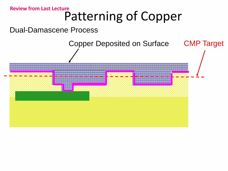
Patterning of Copper
Copper Deposited on Surface
Dual-Damascene Process
CMP Target
Review from Last Lecture
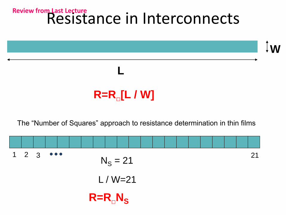
Resistance in Interconnects
R=R□[L / W]
L
W
The “Number of Squares” approach to resistance determination in thin films
1 2 3 21NS = 21
L / W=21
R=R□NS
Review from Last Lecture
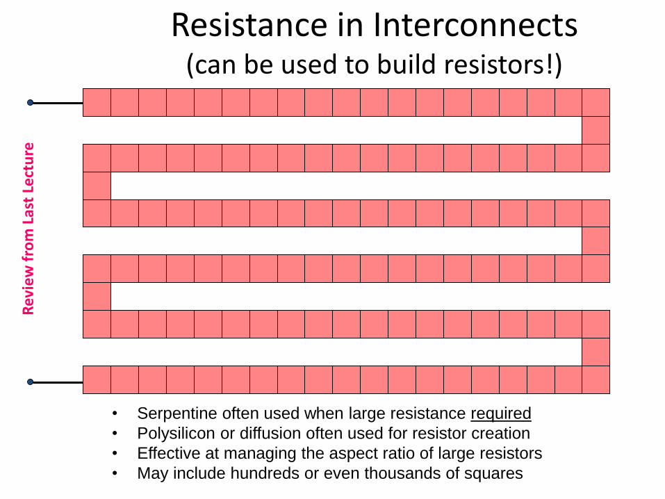
Resistance in Interconnects(can be used to build resistors!)
• Serpentine often used when large resistance required
• Polysilicon or diffusion often used for resistor creation
• Effective at managing the aspect ratio of large resistors
• May include hundreds or even thousands of squares
Rev
iew
fro
m L
ast
Lect
ure
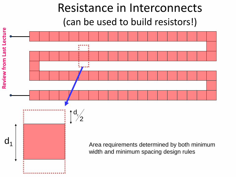
Resistance in Interconnects(can be used to build resistors!)
d1
2d
2
Area requirements determined by both minimum
width and minimum spacing design rules
Rev
iew
fro
m L
ast
Lect
ure
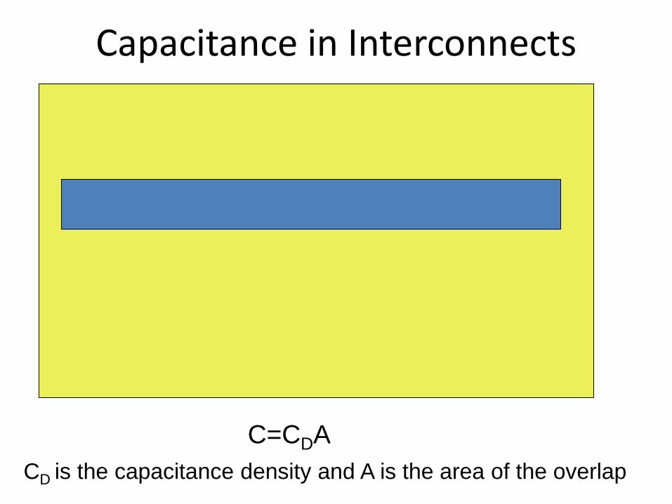
Capacitance in Interconnects
C=CDA
CD is the capacitance density and A is the area of the overlap
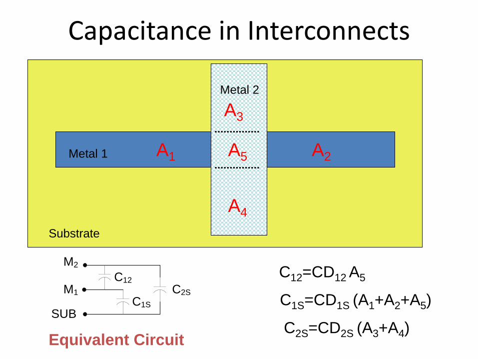
Capacitance in Interconnects
Metal 1
Metal 2
Substrate
A1
A4
A2
A3
A5
C12
C2S
C1S
M1
M2
SUB
Equivalent Circuit
C12=CD12 A5
C1S=CD1S (A1+A2+A5)
C2S=CD2S (A3+A4)
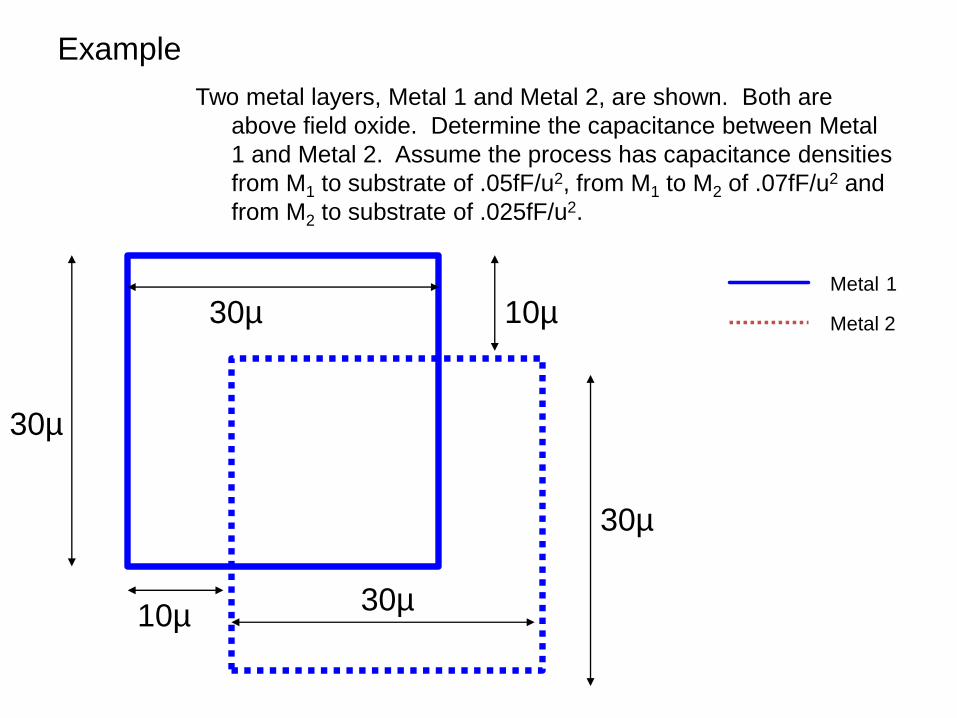
Example
Two metal layers, Metal 1 and Metal 2, are shown. Both are
above field oxide. Determine the capacitance between Metal
1 and Metal 2. Assume the process has capacitance densities
from M1 to substrate of .05fF/u2, from M1 to M2 of .07fF/u2 and
from M2 to substrate of .025fF/u2.
30µ
30µ
30µ
30µ
10µ
10µ
Metal 1
Metal 2
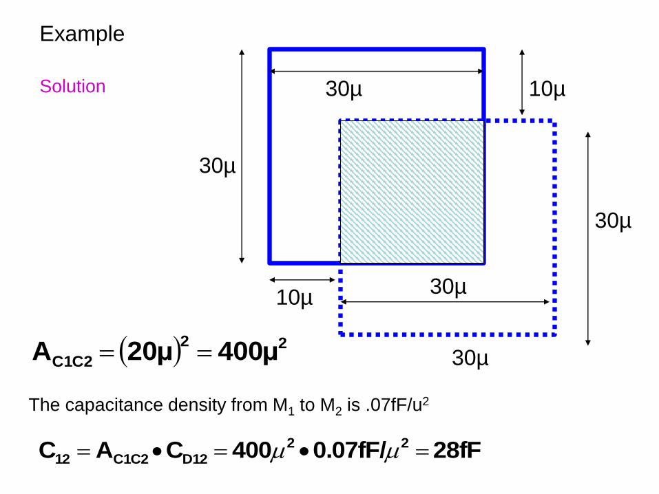
Example
The capacitance density from M1 to M2 is .07fF/u2
30µ
30µ
30µ
30µ
10µ
10µ
Solution
30µ
22
C1C2 400μ20μA
28fF0.07fF/400CAC 22
D12C1C212

Capacitance and Resistance in Interconnects
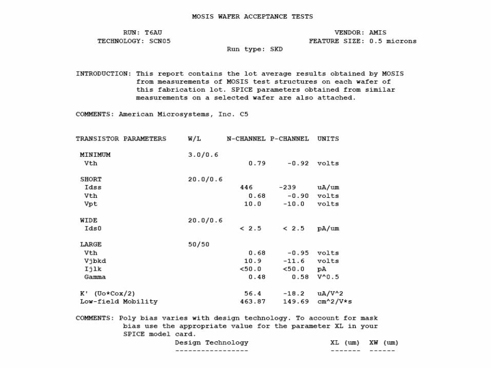
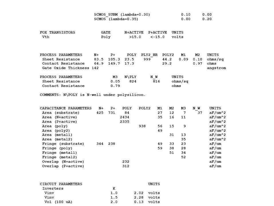
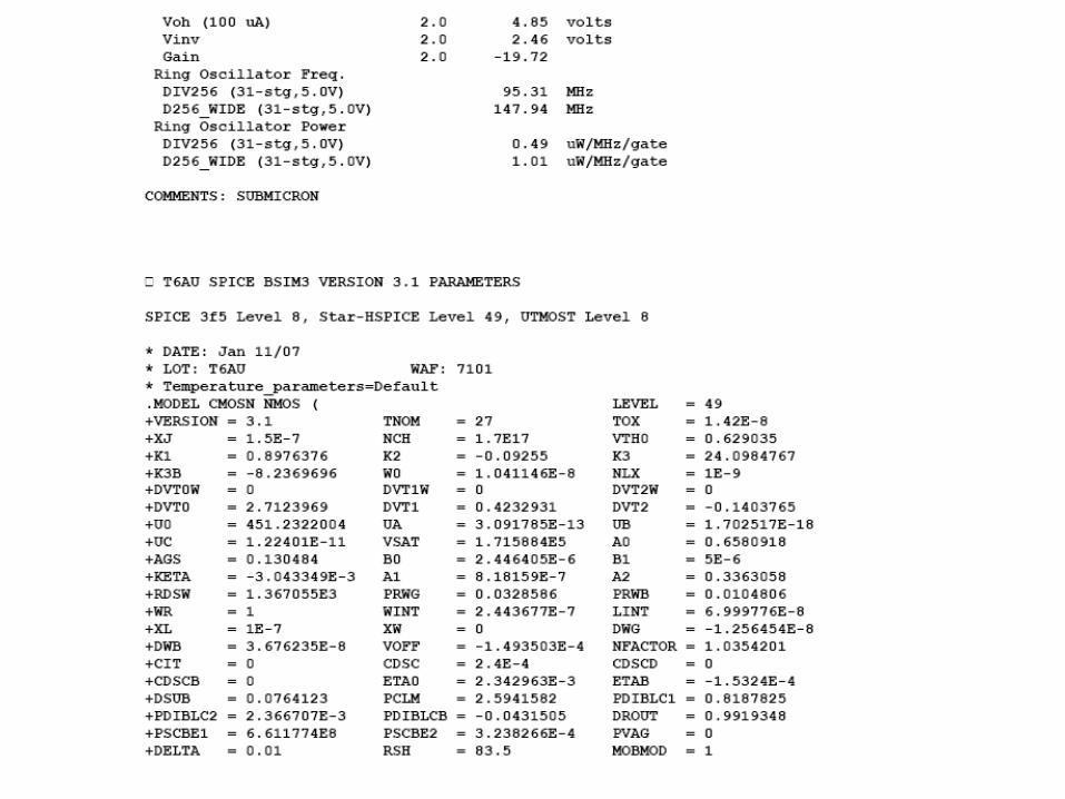
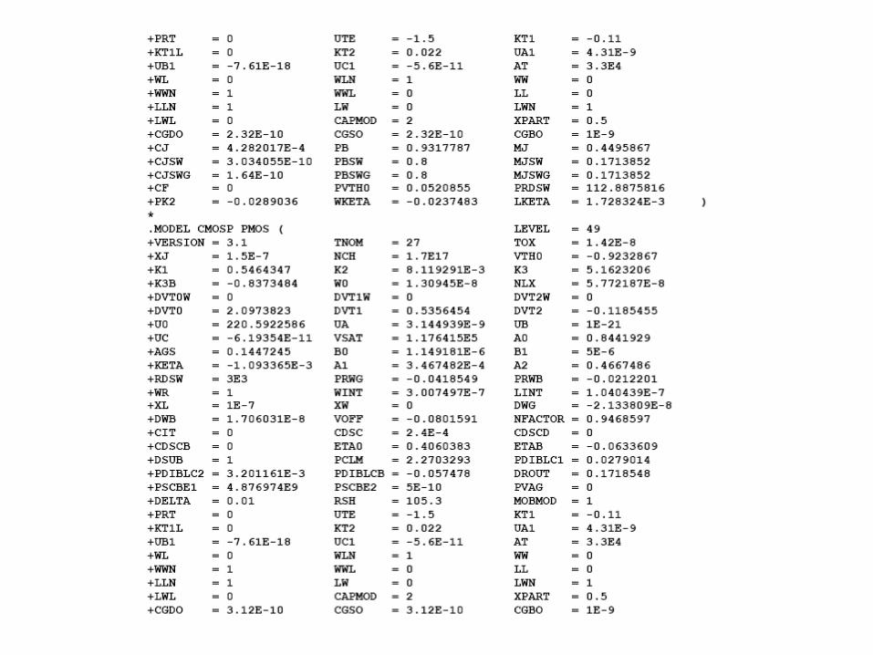
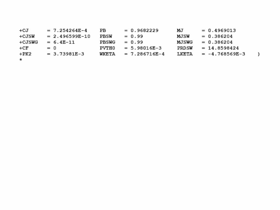
• See MOSIS WEB site for process parameters that characterize parasitic resistances and capacitances
www.mosis.org
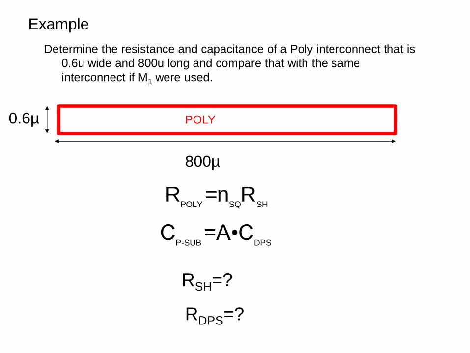
Example
Determine the resistance and capacitance of a Poly interconnect that is
0.6u wide and 800u long and compare that with the same
interconnect if M1 were used.
0.6µ
800µ
POLY
POLY SQ SHR =n R
P-SUB DPSC =A•C
RSH=?
RDPS=?
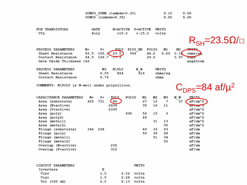
RSH=23.5Ω/□
CDPS=84 af/µ2
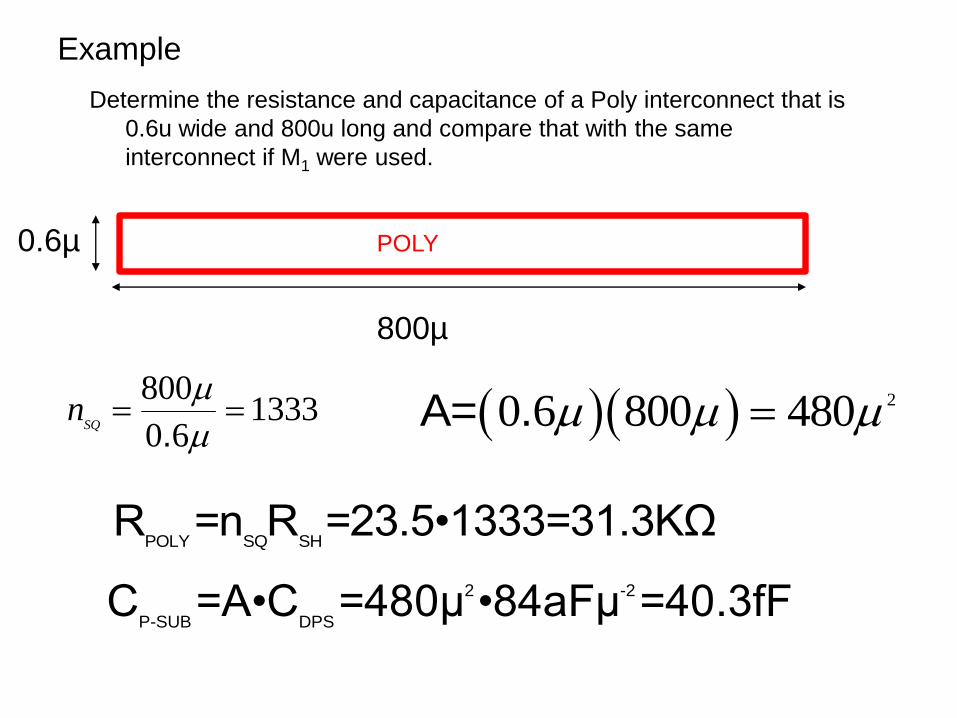
Example
Determine the resistance and capacitance of a Poly interconnect that is
0.6u wide and 800u long and compare that with the same
interconnect if M1 were used.
0.6µ
800µ
8001333
0 6.SQ
n
20 6 800 480A= .
POLY SQ SHR =n R =23.5•1333=31.3KΩ
2 -2
P-SUB DPSC =A•C =480μ •84aFμ =40.3fF
POLY
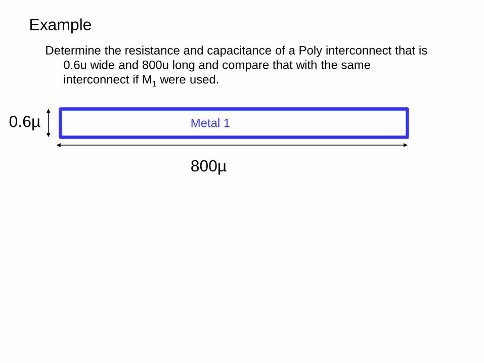
Example
Determine the resistance and capacitance of a Poly interconnect that is
0.6u wide and 800u long and compare that with the same
interconnect if M1 were used.
0.6µ
800µ
Metal 1
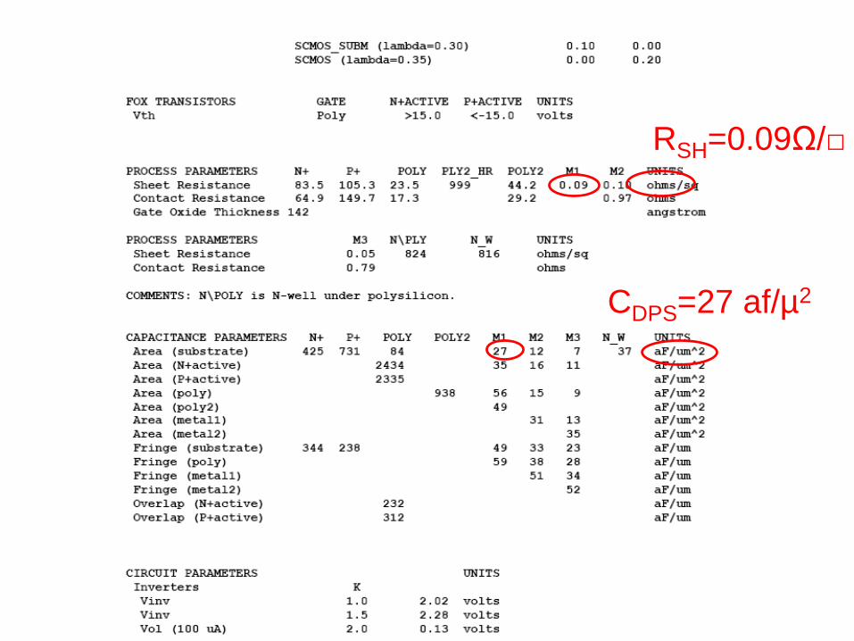
RSH=0.09Ω/□
CDPS=27 af/µ2

Example
Determine the resistance and capacitance of a Poly interconnect that is
0.6u wide and 800u long and compare that with the same
interconnect if M1 were used.
0.6µ
800µ
8001333
0 6.SQ
n
20 6 800 480A= .
M1 SQ SHR =n R =0.09•1333=120Ω
2 -2
M1-SUB DM1SC =A•C =480μ •27aFμ =13.0fF
Metal 1
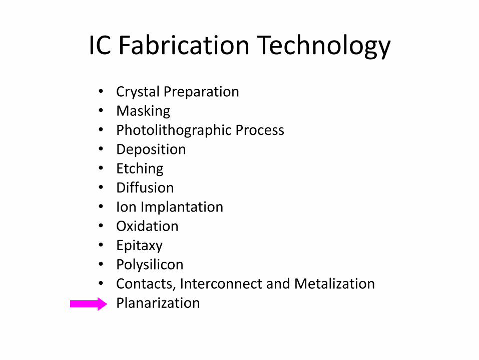
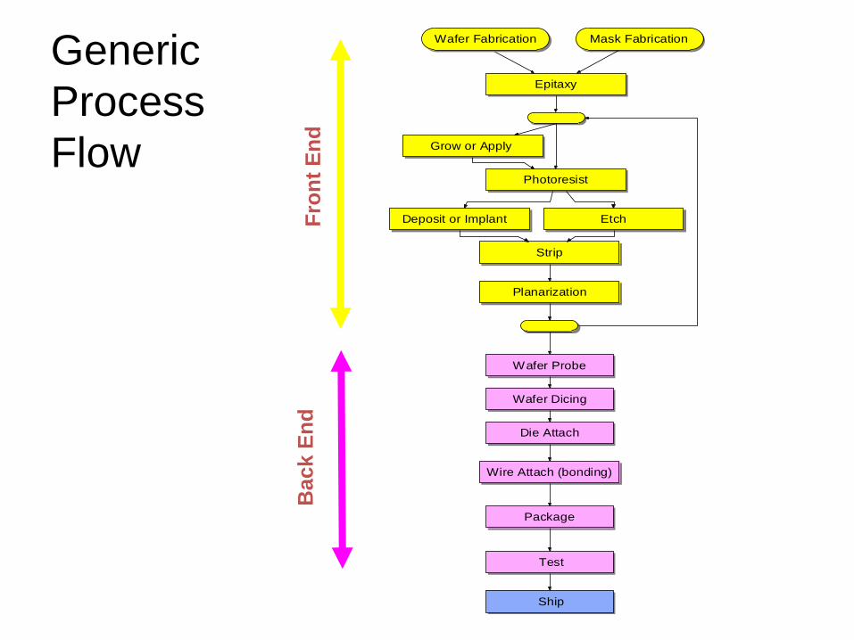
IC Fabrication Technology
• Crystal Preparation• Masking• Photolithographic Process• Deposition• Etching• Diffusion• Ion Implantation• Oxidation• Epitaxy• Polysilicon• Contacts, Interconnect and Metalization• Planarization
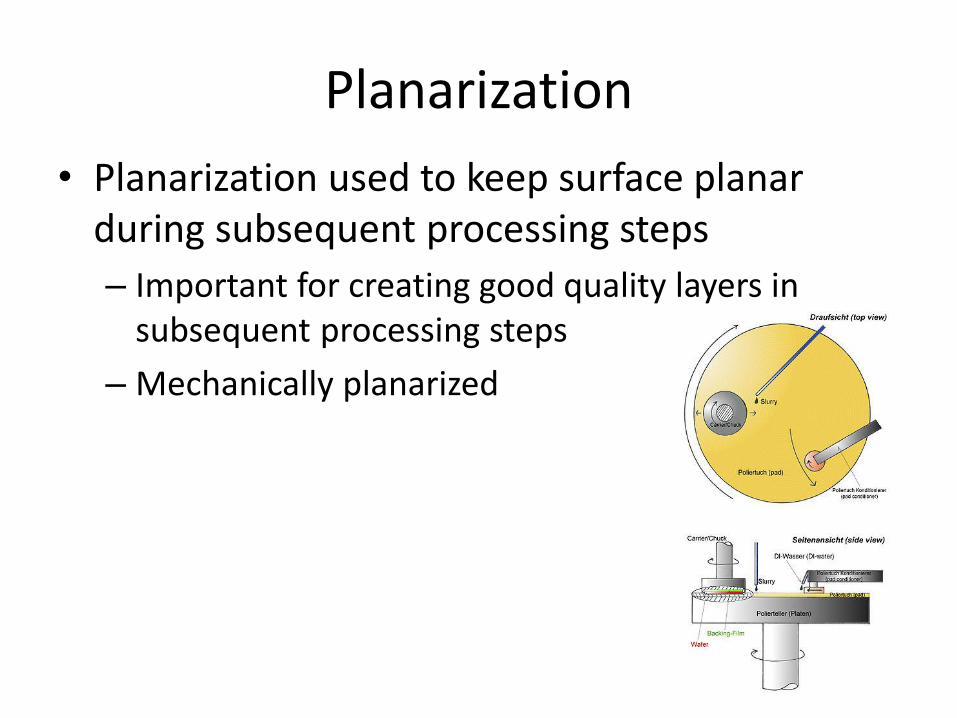
Planarization
• Planarization used to keep surface planar during subsequent processing steps
– Important for creating good quality layers in subsequent processing steps
– Mechanically planarized
Mask Fabrication
Epitaxy
Photoresist
Etch
Strip
Planarization
Deposit or Implant
Grow or Apply
Wafer Probe
Die Attach
Wafer Dicing
Wire Attach (bonding)
Package
Test
Wafer Fabrication
Ship
Fro
nt
En
dB
ack E
nd
Generic
Process
Flow

Front End Process Integration for Fabrication of ICs
Wafer Fabrication Mask Fabrication
Epitaxy
Photoresist
Deposit or Implant Etch
Strip
Planarize
Back End Processing
On
ce
fo
r e
ach
ma
sk
Front-End Process Flow
• Front-end processing steps analogous to a “recipe” for manufacturing an integrated circuit
• Recipes vary from one process to the next but the same basic steps are used throughout the industry
• Details of the recipe are generally considered proprietary
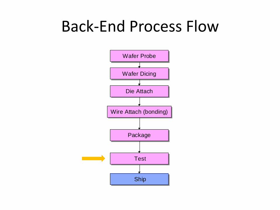
Back-End Process Flow
Wafer Probe
Die Attach
Wafer Dicing
Wire Attach (bonding)
Package
Test
Ship
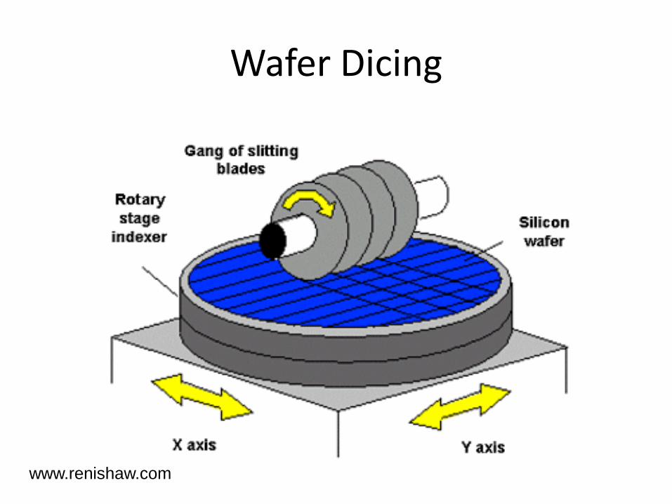
Wafer Dicing
www.renishaw.com
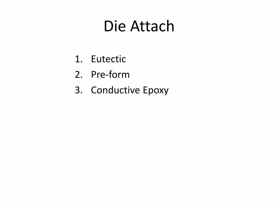
Die Attach
1. Eutectic
2. Pre-form
3. Conductive Epoxy
Electrical Connections (Bonding)
• Wire Bonding
• Bump Bonding
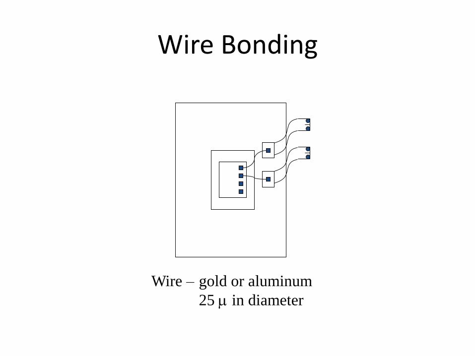
Wire Bonding
Wire – gold or aluminum
25 in diameter
Wire Bonding
Excellent Annimation showing process at :
http://www.kns.com/_Flash/CAP_BONDING_CYCLE.swf

Wire Bonding
www.kns.com
Ball Bond
Wedge Bond
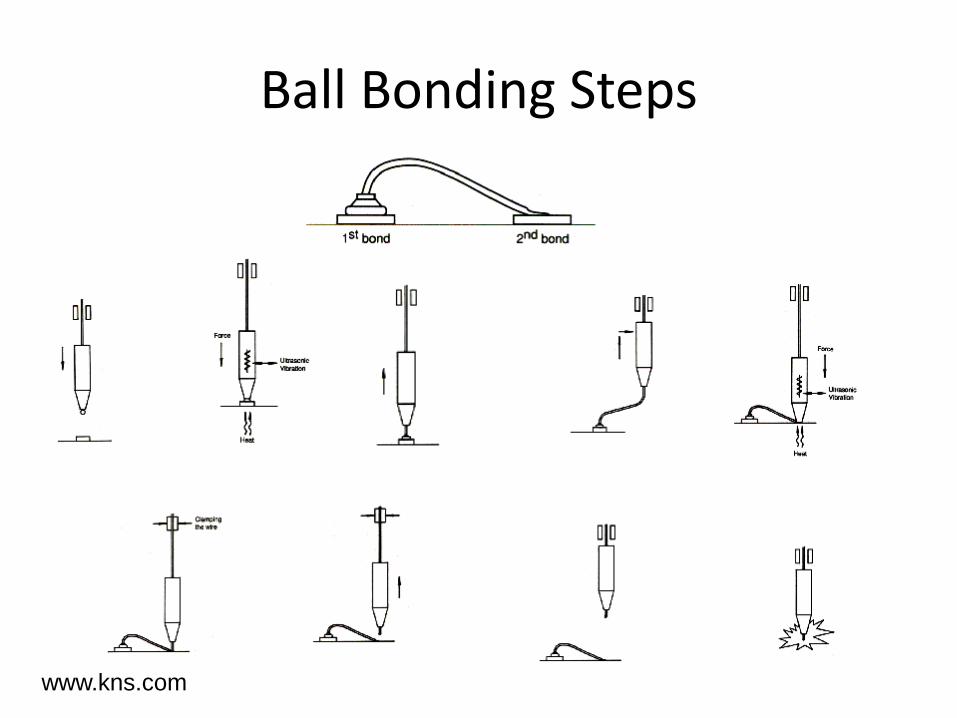
Ball Bonding Steps
www.kns.com
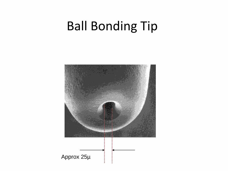
Ball Bonding Tip
Approx 25µ
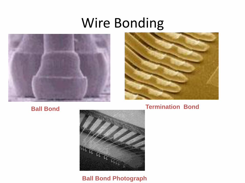
Wire Bonding
Ball Bond Termination Bond
Ball Bond Photograph
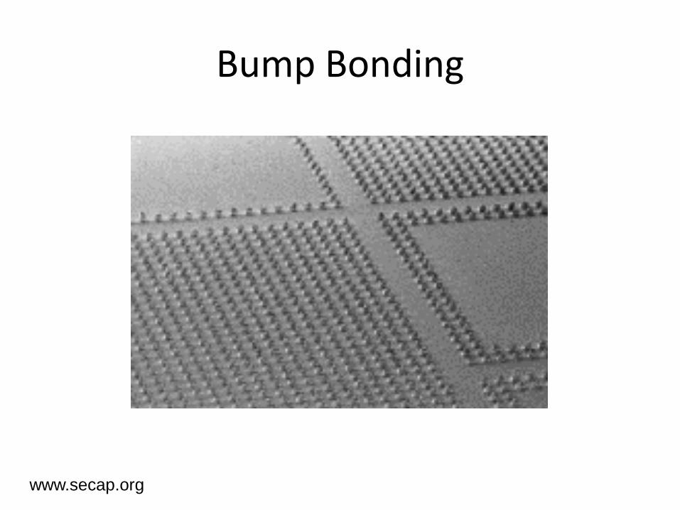
Bump Bonding
www.secap.org
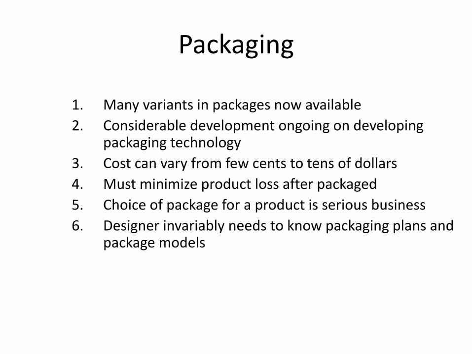
Packaging
1. Many variants in packages now available
2. Considerable development ongoing on developing packaging technology
3. Cost can vary from few cents to tens of dollars
4. Must minimize product loss after packaged
5. Choice of package for a product is serious business
6. Designer invariably needs to know packaging plans and package models
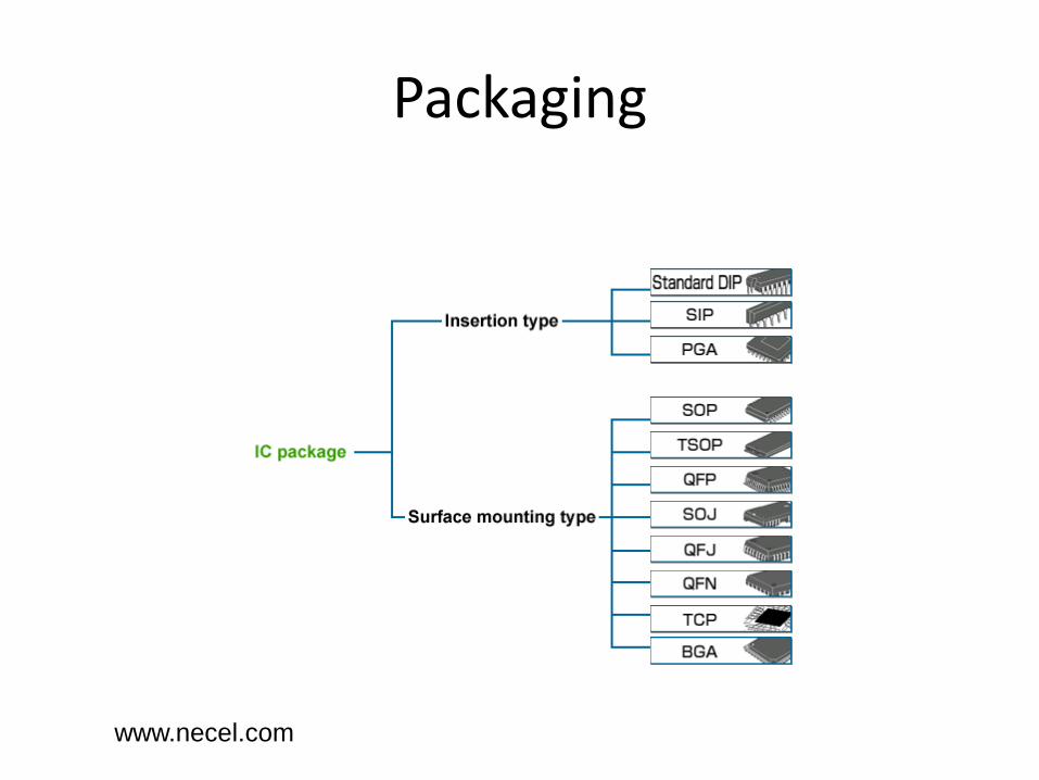
Packaging
www.necel.com
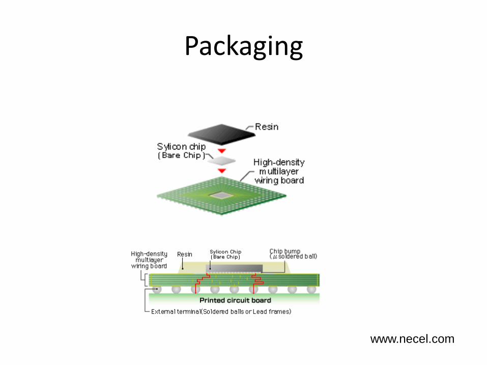
Packaging
www.necel.com
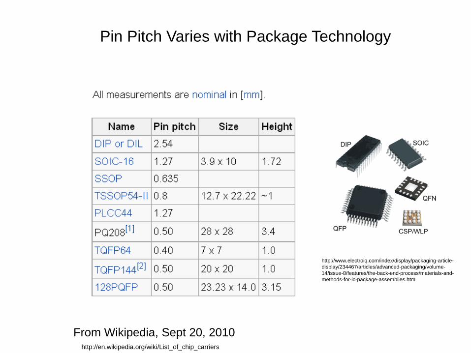
Pin Pitch Varies with Package Technology
From Wikipedia, Sept 20, 2010http://en.wikipedia.org/wiki/List_of_chip_carriers
http://www.electroiq.com/index/display/packaging-article-
display/234467/articles/advanced-packaging/volume-
14/issue-8/features/the-back-end-process/materials-and-
methods-for-ic-package-assemblies.htm
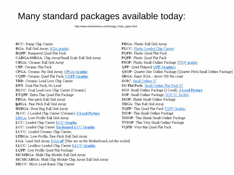
Many standard packages available today:http://www.interfacebus.com/Design_Pack_types.html
Considerable activity today and for years to
come on improving packaging technology
• Multiple die in a package
• Three-dimensional chip stacking
• Multiple levels of interconnect in
stacks
• Through silicon via technology
• Power and heat management
• Cost driven and cost constrained
The following few slides come from a John Lau presentation
Back-End Process Flow
Wafer Probe
Die Attach
Wafer Dicing
Wire Attach (bonding)
Package
Test
Ship
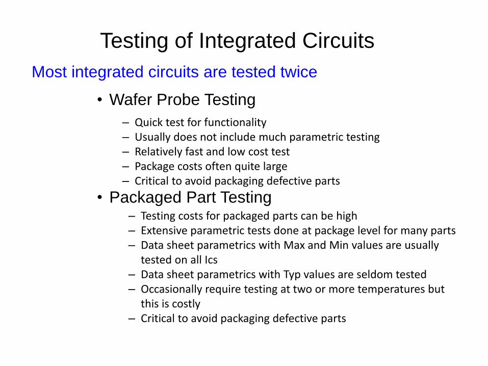
Testing of Integrated Circuits
Most integrated circuits are tested twice
• Wafer Probe Testing
• Packaged Part Testing
– Quick test for functionality – Usually does not include much parametric testing– Relatively fast and low cost test– Package costs often quite large– Critical to avoid packaging defective parts
– Testing costs for packaged parts can be high– Extensive parametric tests done at package level for many parts– Data sheet parametrics with Max and Min values are usually
tested on all Ics– Data sheet parametrics with Typ values are seldom tested– Occasionally require testing at two or more temperatures but
this is costly– Critical to avoid packaging defective parts
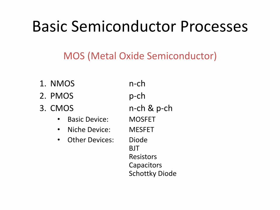
Basic Semiconductor Processes
MOS (Metal Oxide Semiconductor)
1. NMOS n-ch
2. PMOS p-ch
3. CMOS n-ch & p-ch• Basic Device: MOSFET
• Niche Device: MESFET
• Other Devices: DiodeBJTResistorsCapacitorsSchottky Diode

Basic Semiconductor Processes
1. T2L
2. ECL
3. I2L
4. Linear ICs– Basic Device: BJT (Bipolar Junction Transistor)
– Niche Devices: HBJT (Heterojunction Bipolar Transistor)HBT
– Other Devices: DiodeResistorCapacitor
Schottky DiodeJFET (Junction Field Effect Transistor)
Bipolar
Basic Semiconductor Processes
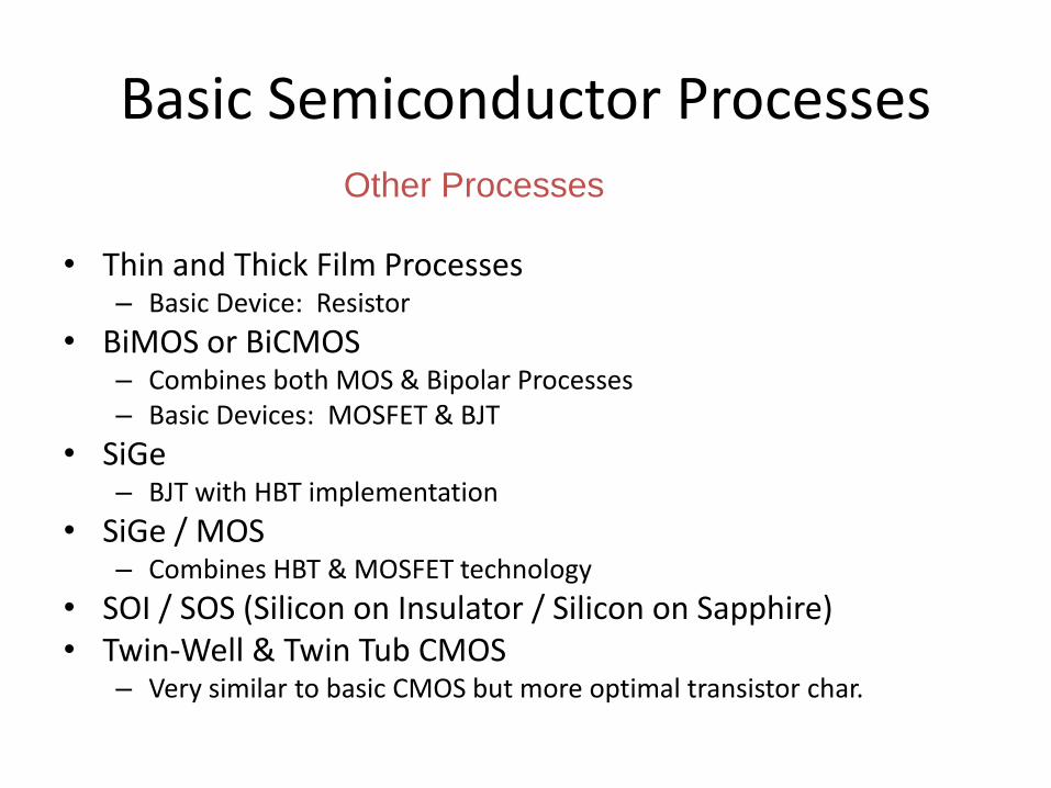
• Thin and Thick Film Processes– Basic Device: Resistor
• BiMOS or BiCMOS– Combines both MOS & Bipolar Processes– Basic Devices: MOSFET & BJT
• SiGe– BJT with HBT implementation
• SiGe / MOS– Combines HBT & MOSFET technology
• SOI / SOS (Silicon on Insulator / Silicon on Sapphire)• Twin-Well & Twin Tub CMOS
– Very similar to basic CMOS but more optimal transistor char.
Other Processes
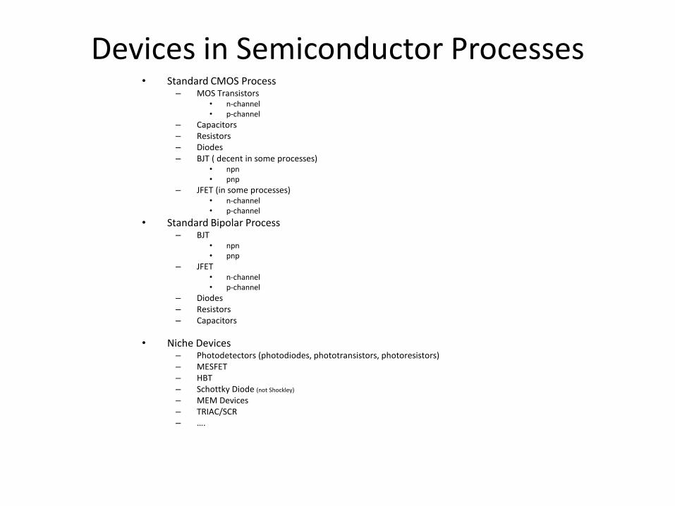
Devices in Semiconductor Processes• Standard CMOS Process
– MOS Transistors• n-channel• p-channel
– Capacitors– Resistors– Diodes– BJT ( decent in some processes)
• npn• pnp
– JFET (in some processes)• n-channel• p-channel
• Standard Bipolar Process– BJT
• npn• pnp
– JFET • n-channel• p-channel
– Diodes– Resistors– Capacitors
• Niche Devices– Photodetectors (photodiodes, phototransistors, photoresistors)– MESFET– HBT– Schottky Diode (not Shockley)
– MEM Devices– TRIAC/SCR– ….

Basic Devices• Standard CMOS Process
– MOS Transistors• n-channel• p-channel
– Capacitors– Resistors– Diodes– BJT (in some processes)
• npn• pnp
– JFET (in some processes)• n-channel• p-channel
• Niche Devices– Photodetectors– MESFET– Schottky Diode (not Shockley)
– MEM Devices– Triac/SCR– ….
Primary Consideration
in This Course
Some Consideration in
This Course
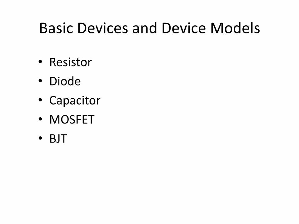
Basic Devices and Device Models
• Resistor
• Diode
• Capacitor
• MOSFET
• BJT
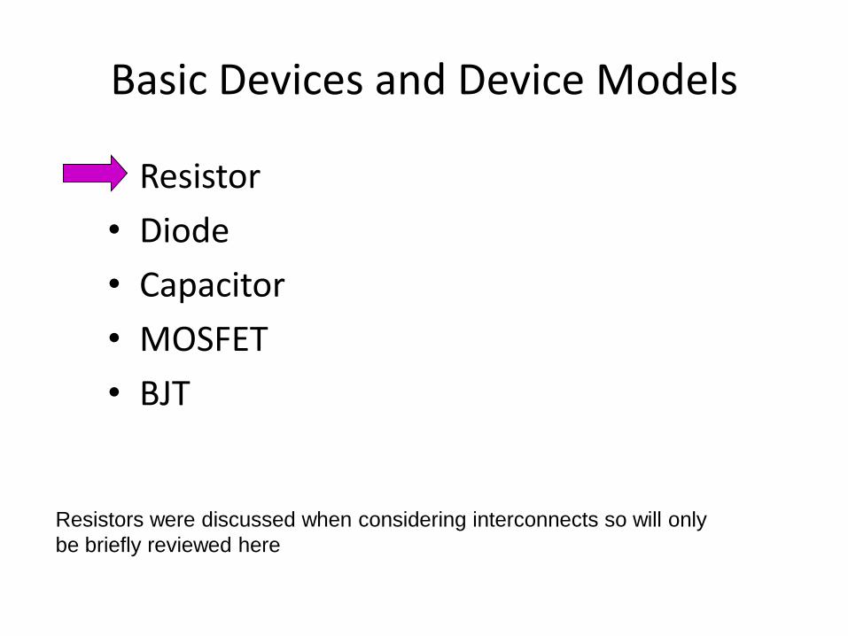
Basic Devices and Device Models
• Resistor
• Diode
• Capacitor
• MOSFET
• BJT
Resistors were discussed when considering interconnects so will only
be briefly reviewed here
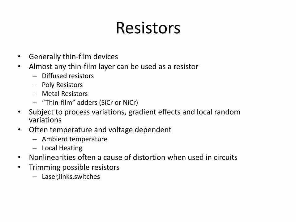
Resistors
• Generally thin-film devices• Almost any thin-film layer can be used as a resistor
– Diffused resistors– Poly Resistors– Metal Resistors– “Thin-film” adders (SiCr or NiCr)
• Subject to process variations, gradient effects and local random variations
• Often temperature and voltage dependent– Ambient temperature– Local Heating
• Nonlinearities often a cause of distortion when used in circuits• Trimming possible resistors
– Laser,links,switches
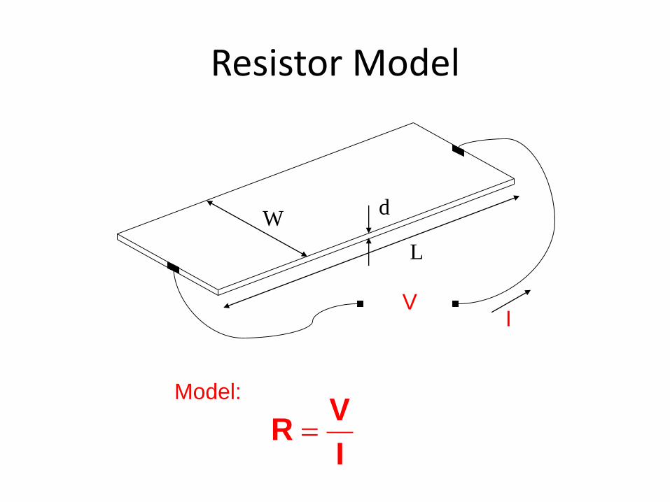
Resistor Model
V
Wd
L
I
I
VR
Model:
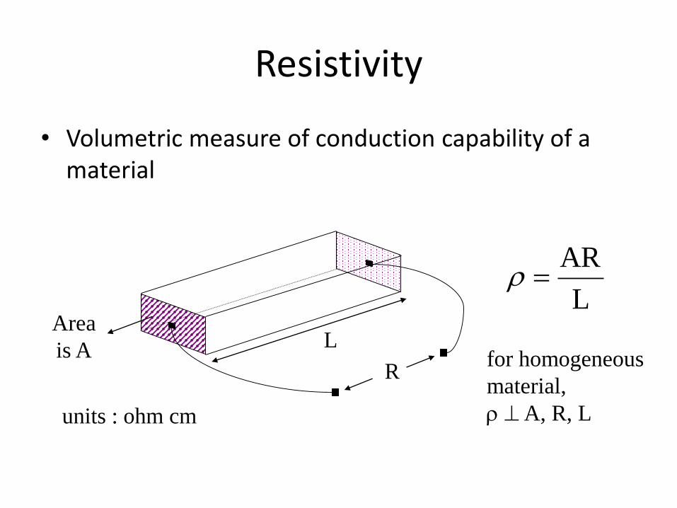
Resistivity
• Volumetric measure of conduction capability of a material
L
R
Area
is A
L
AR
for homogeneous
material,
A, R, Lunits : ohm cm
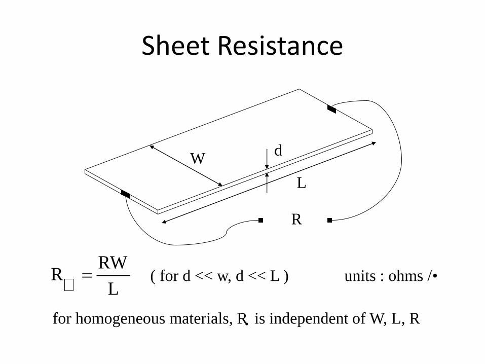
Sheet Resistance
R
Wd
L
L
RW R ( for d << w, d << L ) units : ohms / •
for homogeneous materials, R•is independent of W, L, R
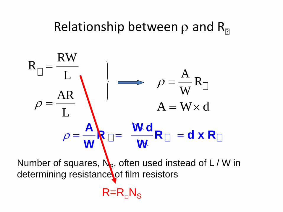
Relationship between and R•
d WA L
AR
RW
A
L
RW R
RxdRW
dW R
W
A
Number of squares, NS, often used instead of L / W in
determining resistance of film resistors
R=R□NS
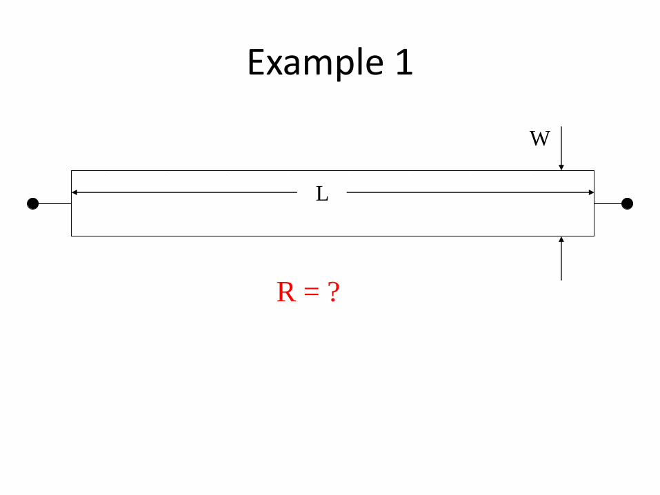
Example 1
W
R = ?
L
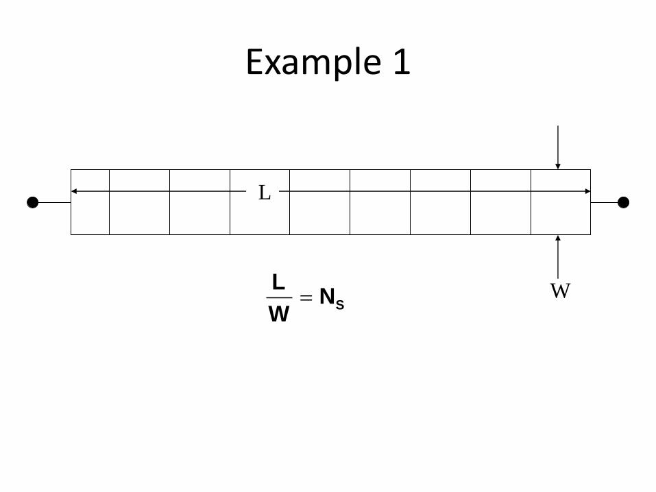
Example 1
W
L
SNW
L
Example 1
.4 8 7 6 5 4 3 2 1
R = ?
Example 1
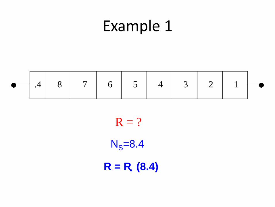
.4 8 7 6 5 4 3 2 1
R = R• (8.4)
R = ?
NS=8.4
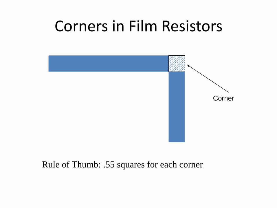
Corners in Film Resistors
Rule of Thumb: .55 squares for each corner
Corner
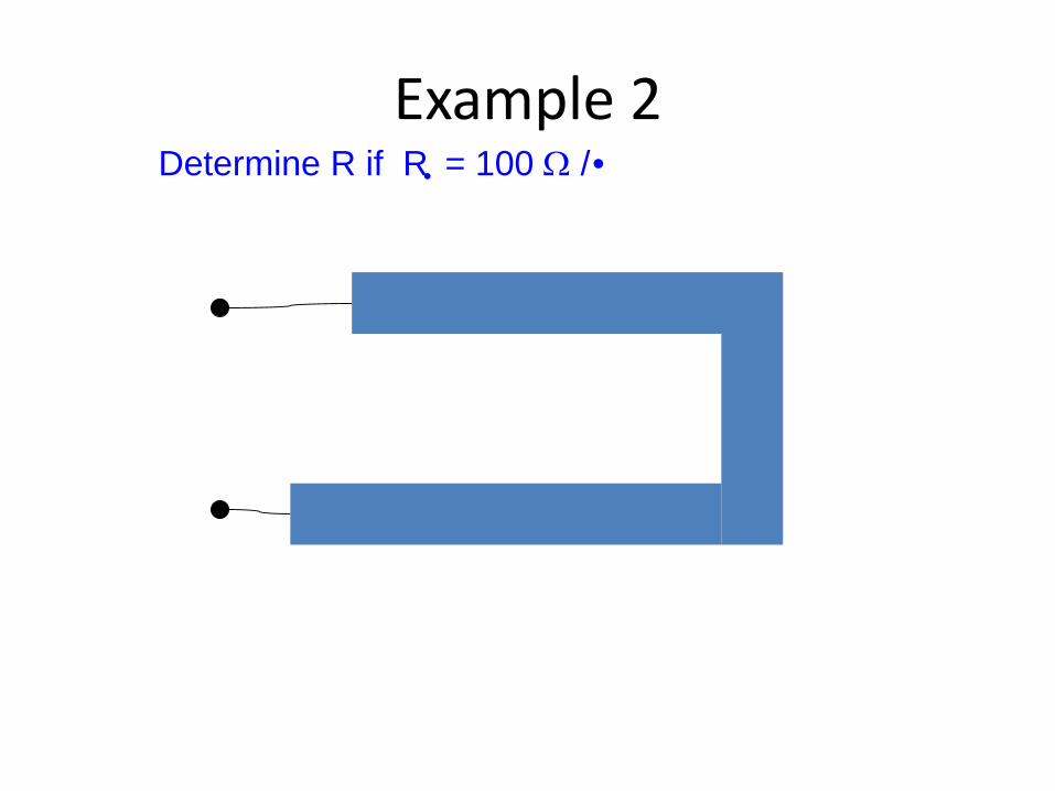
Example 2Determine R if R• = 100 / •
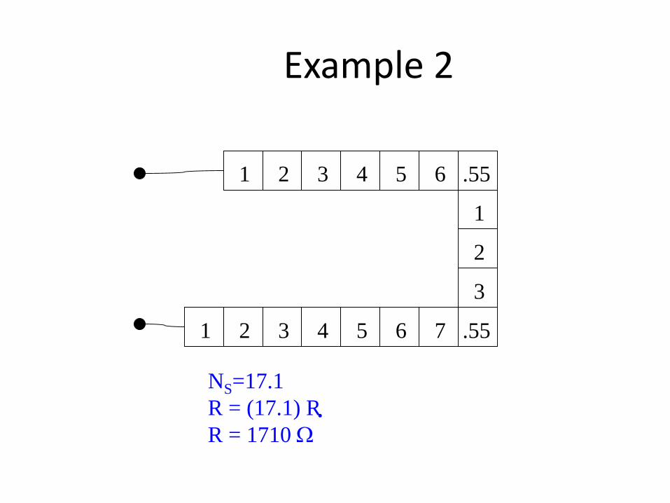
Example 2
1 2 3 4 5 6 .55
1 2 3 4 5 6 7 .55
1
2
3
NS=17.1
R = (17.1) R•
R = 1710
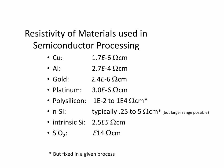
Resistivity of Materials used in Semiconductor Processing
• Cu: 1.7E-6 cm
• Al: 2.7E-4 cm
• Gold: 2.4E-6 cm
• Platinum: 3.0E-6 cm
• Polysilicon: 1E-2 to 1E4 cm*
• n-Si: typically .25 to 5 cm* (but larger range possible)
• intrinsic Si: 2.5E5cm
• SiO2: E14 cm
* But fixed in a given process
End of Lecture 11