EE 330 Lecture 4 - class.ece.iastate.educlass.ece.iastate.edu/ee330/lectures/EE 330 Lect 4 Spring...
77
EE 330 Lecture 4 • Statistics • Key Historical Developments • Initial Device Model • Logic Circuits
Transcript of EE 330 Lecture 4 - class.ece.iastate.educlass.ece.iastate.edu/ee330/lectures/EE 330 Lect 4 Spring...

EE 330
Lecture 4
• Statistics
• Key Historical Developments
• Initial Device Model
• Logic Circuits
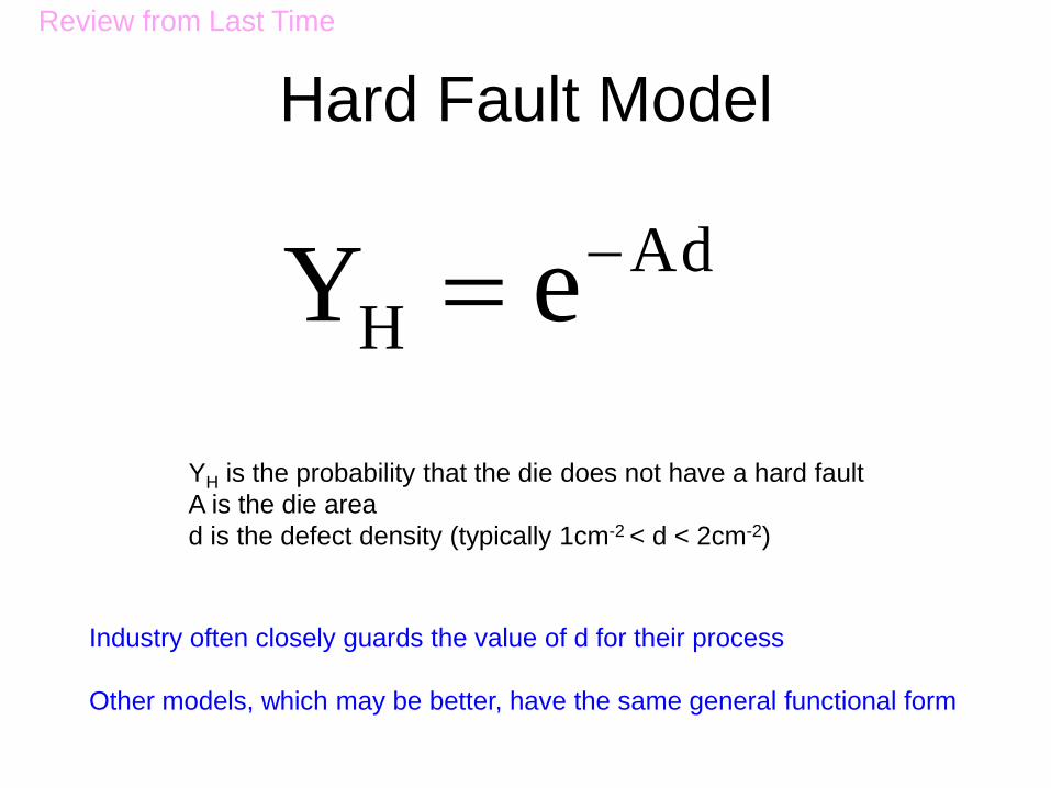
Hard Fault Model
Ad
H eY
YH is the probability that the die does not have a hard fault
A is the die area
d is the defect density (typically 1cm-2 < d < 2cm-2)
Industry often closely guards the value of d for their process
Other models, which may be better, have the same general functional form
Review from Last Time

Overall Yield
If both hard and soft faults affect the yield of
a circuit, the overall yield is given by the
expression
SHYYY
Review from Last Time

Cost Per Good Die
The manufacturing costs per good die is given by
Y
CC FabDie
Good
where CFabDie is the manufacturing costs of a fab die and Y is the yield
There are other costs that must ultimately be included such as testing
costs, engineering costs, etc.
Review from Last Time

Statistics are Real!
Statistics govern what really
happens throughout much of the
engineering field!
Statistics are your Friend !!!!You might as well know what will happen since statistics characterize what
WILL happen in many processes !
Review from Last Time

Meeting the Real Six-Sigma
Challenge
Six-Sigma
or Else !!
Introduced by Bill Smith of Motorola in 1984
2/3 of Fortune 500 Companies adopted/adopting 6-sigma concepts
Review from Last Time

Six-Sigma or Else !!How serious is the “or Else” in the six-sigma programs?
This is not a political advertisement !!

Meeting the Real Six-Sigma
Challenge

Yield at the Six-Sigma level
6-6
162FY N6sigma
(Assume a Gaussian distribution)
Y6sigma=0.9999999980
This is approximately 2 defects out of 1 billion parts

No Yield Defect
Sigma Rate
1 0.682689492 0.317311
2 0.954499736 0.0455
3 0.997300204 0.0027
4 0.999936658 6.33E-05
5 0.999999427 5.73E-07
6 0.9999999980 1.97E-09
7 0.9999999999974 2.56E-12
Yield at Various Sigma Levels
Six-sigma performance is approximately 2 defects in a billion !
n-n

It is assumed that the performance or yield will drop, for some reason, by
1.5 sigma after a process has been established
Initial “six-sigma” solutions really expect only 4.5 sigma performance in
steady-state production
4.5 sigma performance corresponds to 3.4 defects in a million
Six-Sigma
or Else !!
Observation: Any Normally distributed random variable can be mapped to a
N(0,1) random variable by subtracting the mean and dividing by the variance
Assumption : Processes of interest are Gaussian (Normal)

Meeting the Real Six-Sigma
Challenge
Six-Sigma
or Else !!
Highly Statistical Concept !

The Six-Sigma Challenge
Long-term Capability Short-term Capability
Tails are 6.8 parts in a million Tail is 2 parts in a billion
Two-sided capability:
Six Sigma Performance is Very Good !!!
x
f
4.5σ-4.5σ
x
6σ0
f
-6σ

Example: Determine the maximum die area if the circuit
yield is to initially meet the “six sigma” challenge for hard
yield defects (Assume a defect density of 1cm-2 and only
hard yield loss). Is it realistic to set six-sigma die yield
expectations on the design and process engineers?
Solution:
6-6
The “six-sigma” challenge
requires meeting a 6
standard deviation yield with
a Normal (0,1) distribution
162FY N6sigma

Solution cont:
Ad
H eY
d
YlnA H
o22
2-(A)2.5E59cm2.0E
1cm
0.999999998lnA
This is comparable to the area required to fabricate a single transistor
in a state of the art 20nm process
500Å
200Å

Solution cont:
Is it realistic to set six-sigma die hard yield
expectations on the design and process engineers?
The best technologies in the world have orders of
magnitude too many defects to build any useful
integrated circuits with die yields that meet six-sigma
performance requirements !!
Arbitrarily setting six-sigma design
requirements will guarantee financial disaster !!

Meeting the Real Six-Sigma
Challenge
Six-Sigma
or Else !!

Meeting the Real Six-Sigma
Challenge
Six-Sigma
or Else !!
Improving a yield by even one sigma often is
VERY challenging !!

Statistics can be abused !
Many that are not knowledgeable
incorrectly use statistics
Many use statistics to intentionally
mislead the public
Some openly abuse statistics for financial
gain or for manipulation purposes
Keep an open mind to separate “good”
statistics from “abused” statistics

Meeting the Real Six-Sigma
Challenge
Six-Sigma
or Else !!
How has Motorola fared with the 6-sigma approach?
Motorola, Inc. (pronounced ) was an American multinational6 telecommunications
company based in Schaumburg, Illinois, which was eventually divided into two
independent public companies, Motorola Mobility and Motorola Solutions on January
4, 2011, after losing $4.3 billion from 2007 to 2009.7

Meeting the Real Six-Sigma
Challenge
How has Motorola fared with the 6-sigma approach?
• Sold military activities to General Dynamics 2000/2001
• Sold automotive products in 2006
• Spun of discrete components as ON semiconductor in 1999
• Spun of SPS as Freescale in 2003
• Sold Motorola Mobility to Google in 2011
• Motorola Solutions has 23,000 employees, down from over 150,000 in mid ‘90s

http://www.chicagomag.com/Chica
go-Magazine/September-
2014/What-Happened-to-Motorola/

Meeting the Real Six-Sigma
Challenge
Six-Sigma
or Else !!
Six-sigma capability has almost nothing to do with optimizing profits and, if taken
seriously, will likely guarantee a financial fiasco in most manufacturing processes

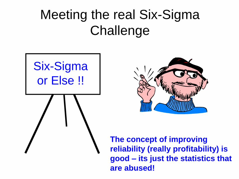
Meeting the real Six-Sigma
Challenge
Six-Sigma
or Else !!
Actually optimizing a
process to six-sigma
performance will almost
always guarantee
financial disaster!

Meeting the real Six-Sigma
Challenge
Six-Sigma
or Else !!
Meeting the real Six-Sigma
Challenge
Six-Sigma
or Else !!
The concept of improving
reliability (really profitability) is
good – its just the statistics that
are abused!

Meeting the real Six-Sigma
Challenge
Six-Sigma
or Else !!
I got the
message

Yield
Variance
Earnings
Per Die
0
6σ
Lo
ss
Pro
fit
-∞
4.5σ
Six-Sigma
or Else !!
The Perception

Six-Sigma
or Else !!
The Reality
Earnings/
Die
0
Lo
ss
Pro
fit
-∞6σ
Yield
Variance
4.5σ
• Designing for 4.5σ or 6σ yield variance will almost always guarantee large losses
• Yield targets should be established to optimize earnings not yield variance

The Perception on Yield
Perception is often that goal should be to get yields as close to 100% as possible
Yield
Earnings/
Die
0
100%
Lo
ss
Pro
fit
-∞

The Reality about Yield
• Return on improving yield when yield is above 95% is small
• Inflection point could be at 99% or higher for some designs but below 50%
for others
• Cost/good die will ultimately go to ∞ as yield approaches 100%
100%80%
CMIN
1.2 CMIN
Cost Per
Good Die
Yield
Designers goal should be to optimize profit, not arbitrary yield target

Key Historical Developments
• 1925,1935 Concept of MOS Transistor Proposed (Lilienfield and Heil)
• 1947 BJT Conceived and Experimentally Verified (Bardeen, Bratin and Shockley of Bell Labs)
• 1959 Jack Kilby (TI) and Bob Noyce (Fairchild) invent IC
• 1963 Wanless (Fairchild) Experimentally verifies MOS Gate

The MOS Transistor (Field Effect Transistor)
Drain
Gate
Source
Initially an idea but little more !

http://www.computerhistory.org/semiconductor/timeline/1926-field.html
Lilienfeld, J. E. "Method and apparatus for controlling
electric currents," U. S. Patent No. 1,745,175 (Filed
October 8, 1926. Issued January 18, 1930).
Lilienfeld, J. E. "Device for controlling electric current," U.
S. Patent No. 1,900,018 (Filed March 28, 1928. Issued
March 7, 1933).
Heil, O. "Improvements in or relating to electrical amplifiers
and other control arrangements and devices," British
Patent No. 439, 457 (Filed March 5, 1935. Issued
December 6, 1935).
1935 Oskar Heil improved MOSFET
https://www.google.com/search?q=Oskar+Heil&biw=1097&bih=568&tbm=isch&imgil=19nt7iXoiQ-
X0M%253A%253B8o3VY91vkR5qnM%253Bhttp%25253A%25252F%25252Fwww.avguide.ch%25252Fmagazin%25252Flautsprecher-made-in-ticino-martin-duerrenmatt-
perfektioniert-den-heil&source=iu&pf=m&fir=19nt7iXoiQ-X0M%253A%252C8o3VY91vkR5qnM%252C_&usg=__67U7QCOIp8tsrLWv8y_YzTy9c7I%3D#imgrc=dv9-
icif2DsZ0M%3A&usg=__67U7QCOIp8tsrLWv8y_YzTy9c7I%3D
Oskar Heil (20 March 1908, in Langwieden – 15
May 1994, San Mateo, California) was a
German electrical engineer and inventor. He
studied physics, chemistry, mathematics, and
music at the Georg-August University of
Göttingen and was awarded his PhD in 1933, for
his work on molecular spectroscopy.
From Wilipedia:


Figures from Heil 1935 patent
Insulated gate controls field between other two terminals

The Vacuum Tube Era
• A major breakthrough in electronics technology
• 6+ decade life span
• Vacuum tube systems not readily affordable by all of society
• Heavy, hot, expensive, large, poor reliability, fragile
The vacuum tube (invented in 1910)
1910 to 1970

The 5-Tube am radio

Philco PT-44
The 5-Tube am radio

The 5-Tube am radio
Schematics were simple !!
(pictures from WEB pages of images)

Lots of people supported the industry (primarily radio, later radio and TV)
with repair shops throughout the country
The Vacuum Tube Era
Tubes as well as resistors and capacitors had poor reliability
(pictures from WEB pages of companies)

The Bipolar Transistor (Bipolar Junction Transistor – BJT)
A solution to a major bottleneck limiting the
development of electronics technology !
Base
Emitter
Collector
Late 1947

Naming the Transistor
From the group at Bell Labs
“We have called it the transistor, T-R-A-N-S-I-S-
T-O-R, because it is resistor or semiconductor
device which can amplify electrical signals as
they are transferred through it from input to
output terminals. It is, if you will, the electrical
equivalent of a vacuum tube amplifier. But there
the similarity ceases. It has no vacuum, no
filament, no glass tube. It is composed entirely
of cold, solid substances.”

http://www.time.com/time/time100/scientist/profile/shockley03.html
William Shockley

William Shockley
He fathered the transistor and brought the silicon to Silicon Valley but is
remembered by many only for his noxious racial views
By GORDON MOORE
The transistor was born just before Christmas 1947 when John Bardeen
and Walter Brattain, two scientists working for William Shockley at Bell
Telephone Laboratories in Murray Hill, N.J., observed that when electrical signals
were applied to contacts on a crystal of germanium, the output power was larger
than the input. Shockley was not present at that first observation. And though he
fathered the discovery in the same way Einstein fathered the atom bomb, by
advancing the idea and pointing the way, he felt left out of the momentous
occasion.
Shockley, a very competitive and sometimes infuriating man, was
determined to make his imprint on the discovery. He searched for an explanation
of the effect from what was then known of the quantum physics of
semiconductors. In a remarkable series of insights made over a few short weeks,
he greatly extended the understanding of semiconductor materials and
developed the underlying theory of another, much more robust amplifying device
— a kind of sandwich made of a crystal with varying impurities added, which
came to be known as the junction transistor. By 1951 Shockley's co-workers
made his semiconductor sandwich and demonstrated that it behaved much as
his theory had predicted.
Gordon Moore

Not content with his lot at Bell Labs, Shockley set out to capitalize on his
invention. In doing so, he played a key role in the industrial development of the region at the
base of the San Francisco Peninsula. It was Shockley who brought the silicon to Silicon
Valley.
In February 1956, with financing from Beckman Instruments Inc., he founded
Shockley Semiconductor Laboratory with the goal of developing and producing a silicon
transistor. He chose to establish this start-up near Palo Alto, where he had grown up and
where his mother still lived. He set up operations in a storefront — little more than a
Quonset hut — and hired a group of young scientists (I was one of them) to develop the
necessary technology. By the spring of 1956 he had a small staff in place and was
beginning to undertake research and development.
…. (in early 1957 a group of the key people involved with Shockley left and
formed a new company named Fairchild Semiconductor …) This new company, financed
by Fairchild Camera & Instrument Corp., became the mother organization for several dozen
new companies in Silicon Valley. Nearly all the scores of companies that are or have been
active in semiconductor technology can trace the technical lineage of their founders back
through Fairchild to the Shockley Semiconductor Laboratory. Unintentionally, Shockley
contributed to one of the most spectacular and successful industry expansions in history.
Editor's note:
In 1963 Shockley left the electronics industry and accepted an appointment at
Stanford. There he became interested in the origins of human intelligence. Although he had
no formal training in genetics or psychology, he began to formulate a theory of what he
called dysgenics. Using data from the U.S. Army's crude pre-induction IQ tests, he
concluded that African Americans were inherently less intelligent than Caucasians — an
analysis that stirred wide controversy among laymen and experts in the field alike.
(Fairchild was formed in 1957 – Moore and Noyce were 2 or 8 co-founders)

The Integrated Circuit


Jack Kilby

Jack Kilby
Kilby’s Integrated Circuit (germanium)

http://www.ti.com/corp/docs/kilbyctr/jackstclair.shtml
There are few men whose insights and professional
accomplishments have changed the world. Jack Kilby is one of these men.
His invention of the monolithic integrated circuit - the microchip - some 45
years ago at Texas Instruments (TI) laid the conceptual and technical
foundation for the entire field of modern microelectronics. It was this
breakthrough that made possible the sophisticated high-speed computers
and large-capacity semiconductor memories of today's information age.
Mr. Kilby grew up in Great Bend, Kansas. With B.S. and M.S.
degrees in electrical engineering from the Universities of Illinois and
Wisconsin respectively, he began his career in 1947 with the Centralab
Division of Globe Union Inc. in Milwaukee, developing ceramic-base, silk-
screen circuits for consumer electronic products.
In 1958, he joined TI in Dallas. During the summer of that year
working with borrowed and improvised equipment, he conceived and built the
first electronic circuit in which all of the components, both active and passive,
were fabricated in a single piece of semiconductor material half the size of a
paper clip. The successful laboratory demonstration of that first simple
microchip on September 12, 1958, made history.
Jack Kilby went on to pioneer military, industrial, and commercial
applications of microchip technology. He headed teams that built both the first
military system and the first computer incorporating integrated circuits. He
later co-invented both the hand-held calculator and the thermal printer that
was used in portable data terminals.


Robert Noyce

Robert Norton Noyce was born December 12, 1927 in Burlington, Iowa.
A noted visionary and natural leader, Robert Noyce helped to create a new
industry when he developed the technology that would eventually become the
microchip. Noted as one of the original computer entrepreneurs, he founded two
companies that would largely shape today’s computer industry—Fairchild
Semiconductor and Intel.
Bob Noyce's nickname was the "Mayor of Silicon Valley." He was one
of the very first scientists to work in the area -- long before the stretch of
California had earned the Silicon name -- and he ran two of the companies that
had the greatest impact on the silicon industry: Fairchild Semiconductor and
Intel. He also invented the integrated chip, one of the stepping stones along the
way to the microprocessors in today's computers.
Noyce, the son of a preacher, grew up in Grinnell, Iowa. He was a
physics major at Grinnell College, and exhibited while there an almost baffling
amount of confidence. He was always the leader of the crowd. This could turn
against him occasionally -- the local farmers didn't approve of him and weren't
likely to forgive quickly when he did something like steal a pig for a college
luau. The prank nearly got Noyce expelled, even though the only reason the
farmer knew about it was because Noyce had confessed and offered to pay for
it.
http://www.ideafinder.com/history/inventors/noyce.htm

While in college, Noyce's physics professor Grant Gale got hold of two
of the very first transistors ever to come out of Bell Labs. Gale showed them off
to his class and Noyce was hooked. The field was young, though, so when
Noyce went to MIT in 1948 for his Ph.D., he found he knew more about
transistors than many of his professors.
After a brief stint making transistors for the electronics firm Philco,
Noyce decided he wanted to work at Shockley Semiconductor. In a single day,
he flew with his wife and two kids to California, bought a house, and went to visit
Shockley to ask for a job -- in that order.
As it was, Shockley and Noyce's scientific vision -- and egos --
clashed. When seven of the young researchers at Shockley semiconductor got
together to consider leaving the company, they realized they needed a leader. All
seven thought Noyce, aged 29 but full of confidence, was the natural choice. So
Noyce became the eighth in the group that left Shockley in 1957 and founded
Fairchild Semiconductor.
Noyce was the general manager of the company and while there
invented the integrated chip -- a chip of silicon with many transistors all etched
into it at once. Fairchild Semiconductor filed a patent for a semiconductor
integrated circuit based on the planar process on July 30, 1959. That was the first
time he revolutionized the semiconductor industry. He stayed with Fairchild until
1968, when he left with Gordon Moore to found Intel.

At Intel he oversaw Ted Hoff's invention of the microprocessor -- that was his
second revolution.
At both companies, Noyce introduced a very casual working
atmosphere, the kind of atmosphere that has become a cultural stereotype of
how California companies work. But along with that open atmosphere came
responsibility. Noyce learned from Shockley's mistakes and he gave his young,
bright employees phenomenal room to accomplish what they wished, in many
ways defining the Silicon Valley working style was his third revolution.

Jack Kilby (34 years old at invention) patent: 3,138,743
Filed Feb 6, 1959 Issued June 23, 1964
Robert Noyce (31 years old at invention) patent: 2,981,877
Filed July 30, 1959 Issued April 25, 1961
The key patents that revolutionized the electronics field:
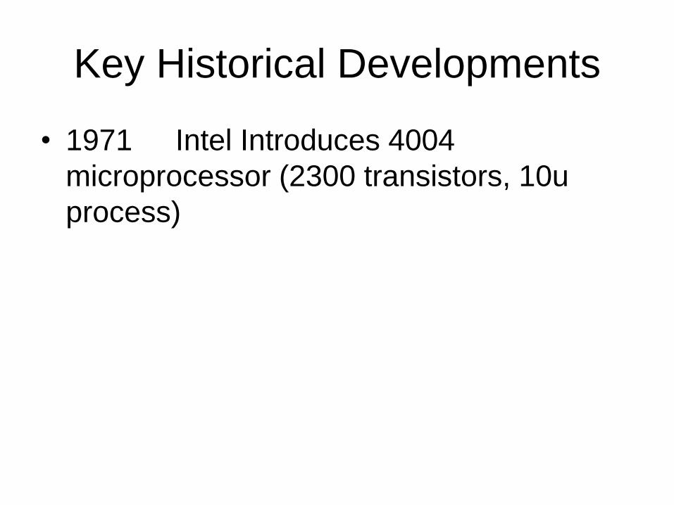
Key Historical Developments
• 1971 Intel Introduces 4004
microprocessor (2300 transistors, 10u
process)


Basic Logic Circuits

Basic Logic Circuits
• Will present a brief description of logic
circuits based upon simple models and
qualitative description of processes
• Will later discuss process technology
needed to develop better models
• Will even later provide more in-depth
discussion of logic circuits based upon
better device models

Models of Devices
• Several models of the electronic devices will be introduced throughout the course
– Complexity
– Accuracy
– Insight
– Application
• Will use the simplest model that can provide acceptable results for any given application

MOS TransistorQualitative Discussion of n-channel Operation
Gate DrainSource
Bulk
n-channel MOSFET
n-type
n+-type
p-type
p+-type
SiO2 (insulator)
POLY (conductor)
Drain
Gate
Source
Drain
Gate
Source
Cross-Sectional
View
Top View
Designer always works with top view
Complete Symmetry in construction between Drain and Source
Symbol for n-channel MOSFET

MOS TransistorQualitative Discussion of n-channel Operation
Gate DrainSource
Bulk
n-channel MOSFET
Drain
Gate
Source
If VGS is large, short circuit exists between drain and source
If VGS is small, open circuit exists between drain and source
Behavioral Description of Operation of n-channel MOS Transistors Created
for use in Basic Digital Circuits
VGS
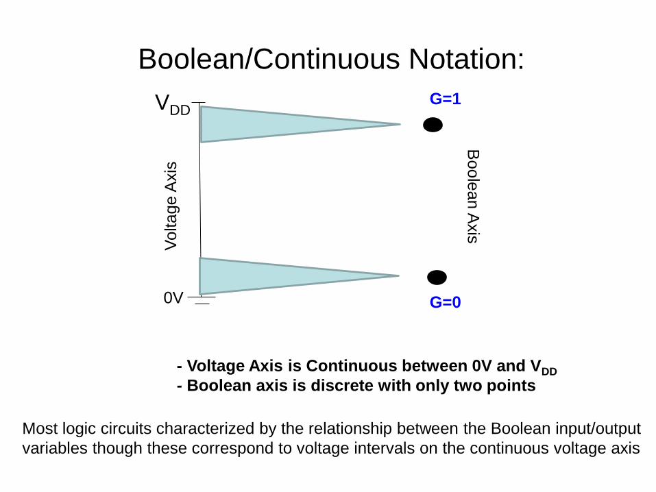
Boolean/Continuous Notation:
VDD
Voltage A
xis
0V G=0
G=1
Boole
an A
xis
- Voltage Axis is Continuous between 0V and VDD
- Boolean axis is discrete with only two points
Most logic circuits characterized by the relationship between the Boolean input/output
variables though these correspond to voltage intervals on the continuous voltage axis

MOS TransistorQualitative Discussion of n-channel Operation
Gate DrainSource
Bulk
n-channel MOSFET
Drain
Gate
Source
D
S
G = 0
D
S
G = 1
Equivalent Circuit for n-channel MOSFET
This is the first model we have for the n-channel MOSFET !
• Source assumed connected
to (or close to) ground
• Boolean G at gate is relative
to ground potential

MOS Transistor MODELDrain
Gate
Source
ID
D
S
G = 0
D
S
G = 1
Equivalent Circuit for n-channel MOSFET
D GS
DS GS
I =0 if V is low
V =0 if V is high
Mathematically:

MOS TransistorQualitative Discussion of p-channel Operation
n-type
n+-type
p-type
p+-type
SiO2 (insulator)
POLY (conductor)
Gate DrainSource
Bulk
p-channel MOSFET
Drain
Gate
Source
Drain
Gate
Source
Cross-Sectional
View
Top View
Complete Symmetry in construction between Drain and Source
Symbol for p-channel MOSFET

MOS TransistorQualitative Discussion of p-channel Operation
Gate DrainSource
Bulk
p-channel MOSFET
Drain
Gate
Source
If VGS is large (and negative), short circuit exists between drain and source
If VGS is small (near 0), open circuit exists between drain and source
Behavioral Description of Operation of p-channel transistors created for use in
basic digital circuits

MOS TransistorQualitative Discussion of p-channel Operation
Gate DrainSource
Bulk
p-channel MOSFET
Drain
Gate
Source
Equivalent Circuit for p-channel MOSFET
D
S
G = 1
D
S
G = 0
This is the first model we have for the p-channel MOSFET !
Source assumed connected
to (or close to) positive VDD and
Boolean G at gate is
relative to ground potential

MOS Transistor MODEL
Equivalent Circuit for p-channel MOSFET
D G GSp
DS G GSp
I =0 if V is high ( V is small)
V =0 if V is low ( V is large)
Mathematically:
Drain
Gate
Source
ID
D
S
G = 1
D
S
G = 0

MOS TransistorComparison of Operation
Drain
Gate
Source
Drain
Gate
Source
D
S
G = 1
D
S
G = 0
D
S
G = 0
D
S
G = 1
Source assumed connected to (or close to) positive VDD
and Boolean G at gate is relative to ground
Source assumed connected
to (or close to) ground

End of Lecture 4