Document Number: MRFE6VP61K25H Technical Data RF...
23
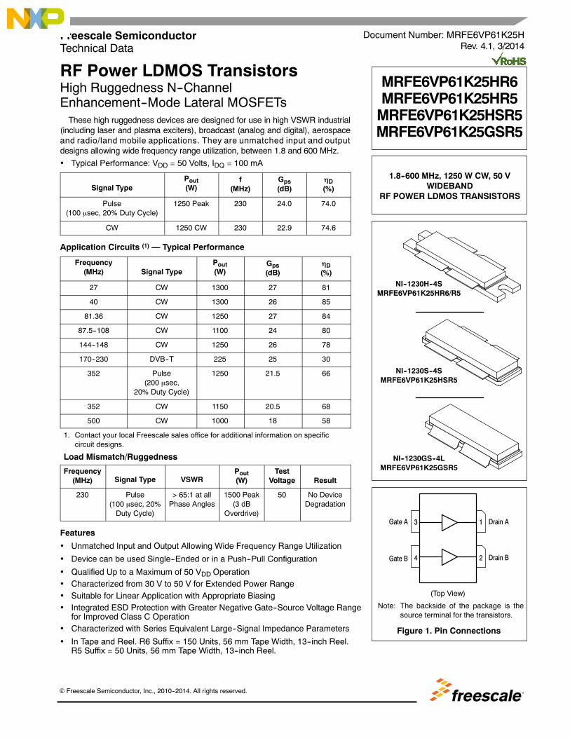
RF Power LDMOS Transistors High Ruggedness N--Channel Enhancement--Mode Lateral MOSFETs These high ruggedness devices are designed for use in high VSWR industrial (including laser and plasma exciters), broadcast (analog and digital), aerospace and radio/land mobile applications. They are unmatched input and output designs allowing wide frequency range utilization, between 1.8 and 600 MHz. Typical Performance: V DD = 50 Volts, I DQ = 100 mA Signal Type P out (W) f (MHz) G ps (dB) D (%) Pulse (100 sec, 20% Duty Cycle) 1250 Peak 230 24.0 74.0 CW 1250 CW 230 22.9 74.6 Application Circuits (1) — Typical Performance Frequency (MHz) Signal Type P out (W) G ps (dB) D (%) 27 CW 1300 27 81 40 CW 1300 26 85 81.36 CW 1250 27 84 87.5--108 CW 1100 24 80 144--148 CW 1250 26 78 170--230 DVB--T 225 25 30 352 Pulse (200 sec, 20% Duty Cycle) 1250 21.5 66 352 CW 1150 20.5 68 500 CW 1000 18 58 1. Contact your local Freescale sales office for additional information on specific circuit designs. Load Mismatch/Ruggedness Frequency (MHz) Signal Type VSWR P out (W) Test Voltage Result 230 Pulse (100 sec, 20% Duty Cycle) > 65:1 at all Phase Angles 1500 Peak (3 dB Overdrive) 50 No Device Degradation Features Unmatched Input and Output Allowing Wide Frequency Range Utilization Device can be used Single--Ended or in a Push--Pull Configuration Qualified Up to a Maximum of 50 V DD Operation Characterized from 30 V to 50 V for Extended Power Range Suitable for Linear Application with Appropriate Biasing Integrated ESD Protection with Greater Negative Gate--Source Voltage Range for Improved Class C Operation Characterized with Series Equivalent Large--Signal Impedance Parameters In Tape and Reel. R6 Suffix = 150 Units, 56 mm Tape Width, 13--inch Reel. R5 Suffix = 50 Units, 56 mm Tape Width, 13--inch Reel. Document Number: MRFE6VP61K25H Rev. 4.1, 3/2014 Freescale Semiconductor Technical Data 1.8--600 MHz, 1250 W CW, 50 V WIDEBAND RF POWER LDMOS TRANSISTORS MRFE6VP61K25HR6 MRFE6VP61K25HR5 MRFE6VP61K25HSR5 MRFE6VP61K25GSR5 (Top View) Drain A 3 1 Figure 1. Pin Connections 4 2 Drain B Gate A Gate B NI--1230H--4S MRFE6VP61K25HR6/R5 NI--1230S--4S MRFE6VP61K25HSR5 Note: The backside of the package is the source terminal for the transistors. NI--1230GS--4L MRFE6VP61K25GSR5 Freescale Semiconductor, Inc., 2010--2014. All rights reserved.
Transcript of Document Number: MRFE6VP61K25H Technical Data RF...
MRFE6VP61K25HR6 MRFE6VP61K25HR5 MRFE6VP61K25HSR5 MRFE6VP61K25GSR5
1RF Device DataFreescale Semiconductor, Inc.
RF Power LDMOS TransistorsHigh Ruggedness N--ChannelEnhancement--Mode Lateral MOSFETsThese high ruggedness devices are designed for use in high VSWR industrial
(including laser and plasma exciters), broadcast (analog and digital), aerospaceand radio/land mobile applications. They are unmatched input and outputdesigns allowing wide frequency range utilization, between 1.8 and 600 MHz.
Typical Performance: VDD = 50 Volts, IDQ = 100 mA
Signal TypePout(W)
f(MHz)
Gps(dB)
D(%)
Pulse(100 sec, 20% Duty Cycle)
1250 Peak 230 24.0 74.0
CW 1250 CW 230 22.9 74.6
Application Circuits (1) — Typical Performance
Frequency(MHz) Signal Type
Pout(W)
Gps(dB)
D(%)
27 CW 1300 27 81
40 CW 1300 26 85
81.36 CW 1250 27 84
87.5--108 CW 1100 24 80
144--148 CW 1250 26 78
170--230 DVB--T 225 25 30
352 Pulse(200 sec,
20% Duty Cycle)
1250 21.5 66
352 CW 1150 20.5 68
500 CW 1000 18 58
1. Contact your local Freescale sales office for additional information on specificcircuit designs.
Load Mismatch/Ruggedness
Frequency(MHz) Signal Type VSWR
Pout(W)
TestVoltage Result
230 Pulse(100 sec, 20%Duty Cycle)
> 65:1 at allPhase Angles
1500 Peak(3 dB
Overdrive)
50 No DeviceDegradation
Features
Unmatched Input and Output Allowing Wide Frequency Range Utilization
Device can be used Single--Ended or in a Push--Pull Configuration
Qualified Up to a Maximum of 50 VDD Operation Characterized from 30 V to 50 V for Extended Power Range Suitable for Linear Application with Appropriate Biasing Integrated ESD Protection with Greater Negative Gate--Source Voltage Range
for Improved Class C Operation Characterized with Series Equivalent Large--Signal Impedance Parameters
In Tape and Reel. R6 Suffix = 150 Units, 56 mm Tape Width, 13--inch Reel.R5 Suffix = 50 Units, 56 mm Tape Width, 13--inch Reel.
Document Number: MRFE6VP61K25HRev. 4.1, 3/2014
Freescale SemiconductorTechnical Data
1.8--600 MHz, 1250 W CW, 50 VWIDEBAND
RF POWER LDMOS TRANSISTORS
MRFE6VP61K25HR6MRFE6VP61K25HR5MRFE6VP61K25HSR5MRFE6VP61K25GSR5
(Top View)
Drain A3 1
Figure 1. Pin Connections
4 2 Drain B
Gate A
Gate B
NI--1230H--4SMRFE6VP61K25HR6/R5
NI--1230S--4SMRFE6VP61K25HSR5
Note: The backside of the package is thesource terminal for the transistors.
NI--1230GS--4LMRFE6VP61K25GSR5
Freescale Semiconductor, Inc., 2010--2014. All rights reserved.
2RF Device Data
Freescale Semiconductor, Inc.
MRFE6VP61K25HR6 MRFE6VP61K25HR5 MRFE6VP61K25HSR5 MRFE6VP61K25GSR5
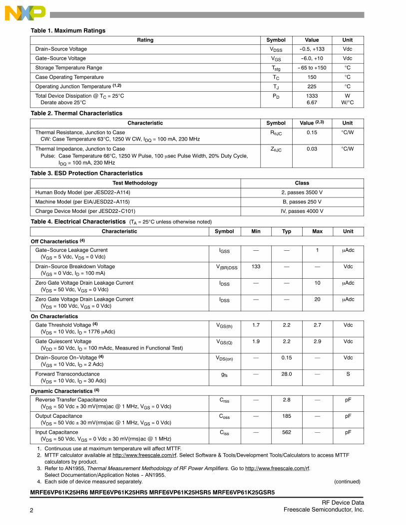
Table 1. Maximum Ratings
Rating Symbol Value Unit
Drain--Source Voltage VDSS --0.5, +133 Vdc
Gate--Source Voltage VGS --6.0, +10 Vdc
Storage Temperature Range Tstg -- 65 to +150 C
Case Operating Temperature TC 150 C
Operating Junction Temperature (1,2) TJ 225 C
Total Device Dissipation @ TC = 25CDerate above 25C
PD 13336.67
WW/C
Table 2. Thermal Characteristics
Characteristic Symbol Value (2,3) Unit
Thermal Resistance, Junction to CaseCW: Case Temperature 63C, 1250 W CW, IDQ = 100 mA, 230 MHz
RJC 0.15 C/W
Thermal Impedance, Junction to CasePulse: Case Temperature 66C, 1250 W Pulse, 100 sec Pulse Width, 20% Duty Cycle,
IDQ = 100 mA, 230 MHz
ZJC 0.03 C/W
Table 3. ESD Protection Characteristics
Test Methodology Class
Human Body Model (per JESD22--A114) 2, passes 3500 V
Machine Model (per EIA/JESD22--A115) B, passes 250 V
Charge Device Model (per JESD22--C101) IV, passes 4000 V
Table 4. Electrical Characteristics (TA = 25C unless otherwise noted)
Characteristic Symbol Min Typ Max Unit
Off Characteristics (4)
Gate--Source Leakage Current(VGS = 5 Vdc, VDS = 0 Vdc)
IGSS — — 1 Adc
Drain--Source Breakdown Voltage(VGS = 0 Vdc, ID = 100 mA)
V(BR)DSS 133 — — Vdc
Zero Gate Voltage Drain Leakage Current(VDS = 50 Vdc, VGS = 0 Vdc)
IDSS — — 10 Adc
Zero Gate Voltage Drain Leakage Current(VDS = 100 Vdc, VGS = 0 Vdc)
IDSS — — 20 Adc
On Characteristics
Gate Threshold Voltage (4)
(VDS = 10 Vdc, ID = 1776 Adc)VGS(th) 1.7 2.2 2.7 Vdc
Gate Quiescent Voltage(VDD = 50 Vdc, ID = 100 mAdc, Measured in Functional Test)
VGS(Q) 1.9 2.2 2.9 Vdc
Drain--Source On--Voltage (4)
(VGS = 10 Vdc, ID = 2 Adc)VDS(on) — 0.15 — Vdc
Forward Transconductance(VDS = 10 Vdc, ID = 30 Adc)
gfs — 28.0 — S
Dynamic Characteristics (4)
Reverse Transfer Capacitance(VDS = 50 Vdc 30 mV(rms)ac @ 1 MHz, VGS = 0 Vdc)
Crss — 2.8 — pF
Output Capacitance(VDS = 50 Vdc 30 mV(rms)ac @ 1 MHz, VGS = 0 Vdc)
Coss — 185 — pF
Input Capacitance(VDS = 50 Vdc, VGS = 0 Vdc 30 mV(rms)ac @ 1 MHz)
Ciss — 562 — pF
1. Continuous use at maximum temperature will affect MTTF.2. MTTF calculator available at http://www.freescale.com/rf. Select Software & Tools/Development Tools/Calculators to access MTTF
calculators by product.3. Refer to AN1955, Thermal Measurement Methodology of RF Power Amplifiers. Go to http://www.freescale.com/rf.
Select Documentation/Application Notes -- AN1955.4. Each side of device measured separately. (continued)
MRFE6VP61K25HR6 MRFE6VP61K25HR5 MRFE6VP61K25HSR5 MRFE6VP61K25GSR5
3RF Device DataFreescale Semiconductor, Inc.
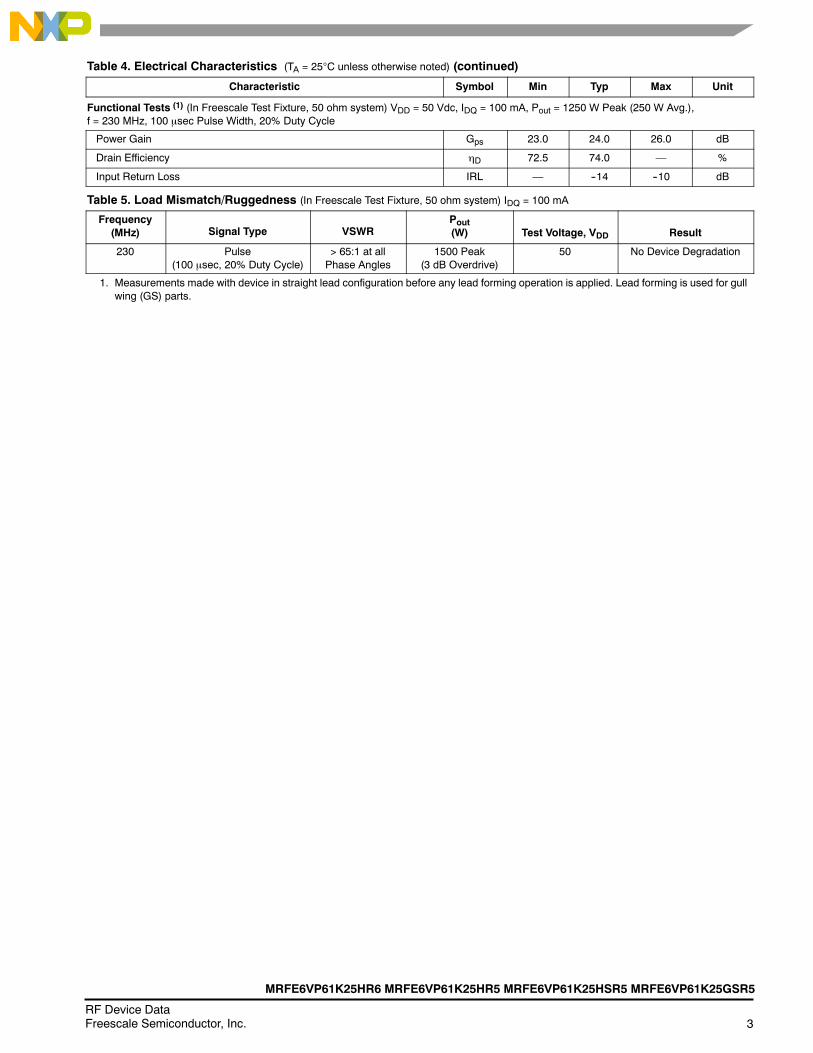
Table 4. Electrical Characteristics (TA = 25C unless otherwise noted) (continued)
Characteristic Symbol Min Typ Max Unit
Functional Tests (1) (In Freescale Test Fixture, 50 ohm system) VDD = 50 Vdc, IDQ = 100 mA, Pout = 1250 W Peak (250 W Avg.),f = 230 MHz, 100 sec Pulse Width, 20% Duty Cycle
Power Gain Gps 23.0 24.0 26.0 dB
Drain Efficiency D 72.5 74.0 — %
Input Return Loss IRL — --14 --10 dB
Table 5. Load Mismatch/Ruggedness (In Freescale Test Fixture, 50 ohm system) IDQ = 100 mA
Frequency(MHz) Signal Type VSWR
Pout(W) Test Voltage, VDD Result
230 Pulse(100 sec, 20% Duty Cycle)
> 65:1 at allPhase Angles
1500 Peak(3 dB Overdrive)
50 No Device Degradation
1. Measurements made with device in straight lead configuration before any lead forming operation is applied. Lead forming is used for gullwing (GS) parts.

4RF Device Data
Freescale Semiconductor, Inc.
MRFE6VP61K25HR6 MRFE6VP61K25HR5 MRFE6VP61K25HSR5 MRFE6VP61K25GSR5
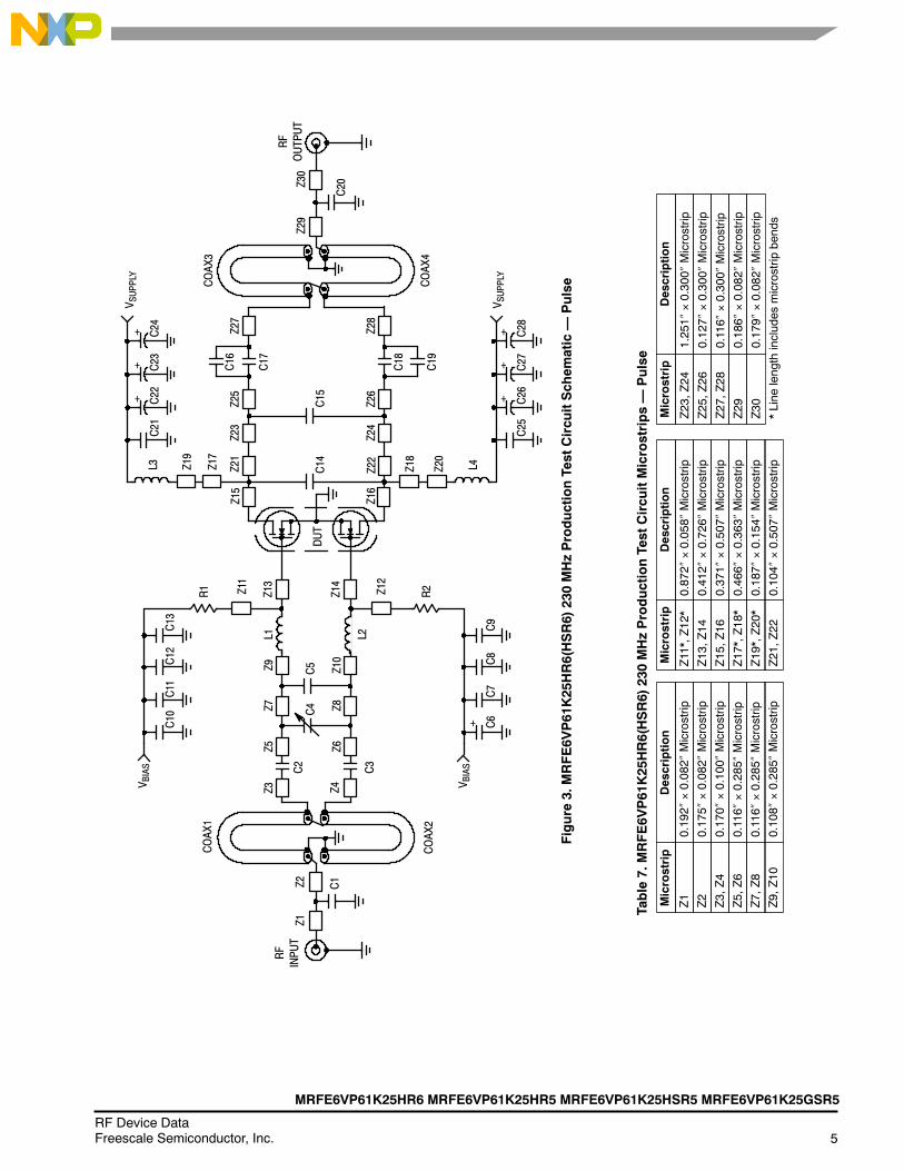
Figure 2. MRFE6VP61K25HR6(HSR6) 230 MHz Production Test Circuit Component Layout — Pulse
-- --
-- --
CUTOUTAREA
C10 C11 C12C13
R1
C1
C2
C3
C4 L1
C5
L2
R2
C9C7 C8C6
COAX2
COAX1
COAX4
COAX3
C14
C22 C23 C24
C21
L3
C15
C16
C17
C18
C19C20
C26 C27 C28
L4
MRFE6VP61K25HRev. 3
C25
Table 6. MRFE6VP61K25HR6(HSR6) 230 MHz Production Test Circuit Component Designations and Values — PulsePart Description Part Number Manufacturer
C1 20 pF Chip Capacitor ATC100B200JT500XT ATC
C2, C3, C5 27 pF Chip Capacitors ATC100B270JT500XT ATC
C4 0.8--8.0 pF Variable Capacitor, Gigatrim 27291SL Johanson
C6, C10 22 F, 35 V Tantalum Capacitors T491X226K035AT Kemet
C7, C11 0.1 F Chip Capacitors CDR33BX104AKYS AVX
C8, C12 220 nF Chip Capacitors C1812C224K5RACTU Kemet
C9, C13, C21, C25 1000 pF Chip Capacitors ATC100B102JT50XT ATC
C14 43 pF Chip Capacitor ATC100B430JT500XT ATC
C15 75 pF Metal Mica MIN02--002EC750J--F CDE
C16, C17, C18, C19 240 pF Chip Capacitors ATC100B241JT200XT ATC
C20 6.2 pF Chip Capacitor ATC100B6R2BT500XT ATC
C22, C23, C24, C26, C27, C28 470 F, 63 V Electrolytic Capacitors MCGPR63V477M13X26--RH Multicomp
Coax1, 2, 3, 4 25 Semi Rigid Coax, 2.2 Shield Length UT--141C--25 Micro--Coax
L1, L2 5 nH Inductors A02TKLC Coilcraft
L3, L4 6.6 nH Inductors GA3093--ALC Coilcraft
R1, R2 10 Chip Resistors CRCW120610R0JNEA Vishay
PCB 0.030, r = 2.55 AD255A Arlon
MRFE6VP61K25HR6 MRFE6VP61K25HR5 MRFE6VP61K25HSR5 MRFE6VP61K25GSR5
5RF Device DataFreescale Semiconductor, Inc.
+
+
+
+
+
+
+
RF
INPUT
Z1Z2
Z3
C3
Z4C1
COAX1
COAX2
Z5
C2
Z6
Z7 Z8
Z9 Z10
C4
C5
V BIAS
L1 L2
V BIAS
C10
C11
C12
C13
C6
C7
C8
C9
R1
R2Z11
Z13
Z14
DUT
Z12
Z15
Z16
L3 Z19
Z17
Z21
Z22
Z18
Z20
Z23
Z25
Z24
Z26
C14
C15
L4
C21
C22
C23
C24
C25
C26
C27
C28Z27
Z28
C16
C17
C18
C19
COAX4
COAX3
Z29
Z30
C20
RF
OUTPUT
V SUPPLY
V SUPPLY
Table7.MRFE6V
P61K25HR6(HSR6)230MHzProductionTestCircuitMicrostrips—
Pulse
Description
Microstrip
Description
Microstrip
Description
Microstrip
Z1
0.192
0.082
Microstrip
Z2
0.175
0.082
Microstrip
Z3,Z4
0.170
0.100
Microstrip
Z5,Z6
0.116
0.285
Microstrip
Z7,Z8
0.116
0.285
Microstrip
Z9,Z10
0.108
0.285
Microstrip
Figure
3.MRFE6V
P61K25HR6(HSR6)230MHzProductionTestCircuitSchem
atic—
Pulse
Z11*,Z12*
0.872
0.058
Microstrip
Z13,Z14
0.412
0.726
Microstrip
Z15,Z16
0.371
0.507
Microstrip
Z17*,Z18*
0.466
0.363
Microstrip
Z19*,Z20*
0.187
0.154
Microstrip
Z21,Z22
0.104
0.507
Microstrip
Z23,Z24
1.251
0.300
Microstrip
Z25,Z26
0.127
0.300
Microstrip
Z27,Z28
0.116
0.300
Microstrip
Z29
0.186
0.082
Microstrip
Z30
0.179
0.082
Microstrip
*Line
lengthincludes
microstrip
bends
6RF Device Data
Freescale Semiconductor, Inc.
MRFE6VP61K25HR6 MRFE6VP61K25HR5 MRFE6VP61K25HSR5 MRFE6VP61K25GSR5
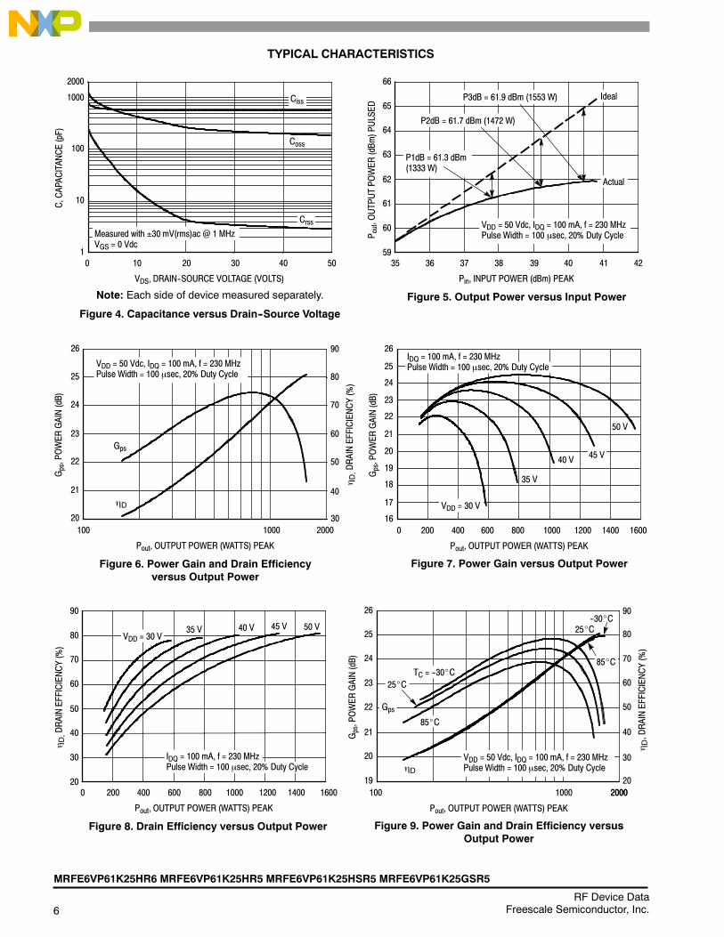
TYPICAL CHARACTERISTICS
50
10
2000
0 2010
VDS, DRAIN--SOURCE VOLTAGE (VOLTS)
Figure 4. Capacitance versus Drain--Source Voltage
C,CAPACITANCE(pF)
30
Ciss1000
100
40
Coss
Measured with 30 mV(rms)ac @ 1 MHzVGS = 0 Vdc
Note: Each side of device measured separately.
1 59
66
35
Pin, INPUT POWER (dBm) PEAK
Figure 5. Output Power versus Input Power
64
36 37 38 39 40 41 42
P out,OUTPUTPOWER
(dBm
)PULSED
63
60
Actual
Ideal
VDD = 50 Vdc, IDQ = 100 mA, f = 230 MHzPulse Width = 100 sec, 20% Duty Cycle
P1dB = 61.3 dBm(1333 W)
62
61
65P3dB = 61.9 dBm (1553 W)
P2dB = 61.7 dBm (1472 W)
26
30
90
100
24 70
50
Pout, OUTPUT POWER (WATTS) PEAK
Figure 6. Power Gain and Drain Efficiencyversus Output Power
Gps,POWER
GAIN(dB)
D,DRAINEFFICIENCY(%)
22
202000
21 40
60
80
23
25
16
23
0
20
19
Pout, OUTPUT POWER (WATTS) PEAK
Figure 7. Power Gain versus Output Power
Gps,POWER
GAIN(dB)
200
18
1400 1600
17
400 800 1000 1200
VDD = 30 V
50 V21
22
25
24
26
600
35 V
40 V 45 V
20
90
0
Pout, OUTPUT POWER (WATTS) PEAK
Figure 8. Drain Efficiency versus Output Power
70
200 400 600 800 1000 1200 1400
60
30
50
40
80
1600
Figure 9. Power Gain and Drain Efficiency versusOutput Power
Pout, OUTPUT POWER (WATTS) PEAK
Gps,POWER
GAIN(dB)
19
21
20
100 2000
D
25_CTC = --30_C
85_C
Gps
40
60
50
20
30
D,DRAINEFFICIENCY(%)
--30_C25_C
85_C
VDD = 30 V50 V35 V 40 V 45 V
D,DRAINEFFICIENCY(%)
24
23
22
26
25
70
80
90
Crss
1000
D
Gps
VDD = 50 Vdc, IDQ = 100 mA, f = 230 MHzPulse Width = 100 sec, 20% Duty Cycle
20001000
IDQ = 100 mA, f = 230 MHzPulse Width = 100 sec, 20% Duty Cycle
IDQ = 100 mA, f = 230 MHzPulse Width = 100 sec, 20% Duty Cycle
VDD = 50 Vdc, IDQ = 100 mA, f = 230 MHzPulse Width = 100 sec, 20% Duty Cycle
MRFE6VP61K25HR6 MRFE6VP61K25HR5 MRFE6VP61K25HSR5 MRFE6VP61K25GSR5
7RF Device DataFreescale Semiconductor, Inc.
TYPICAL CHARACTERISTICS
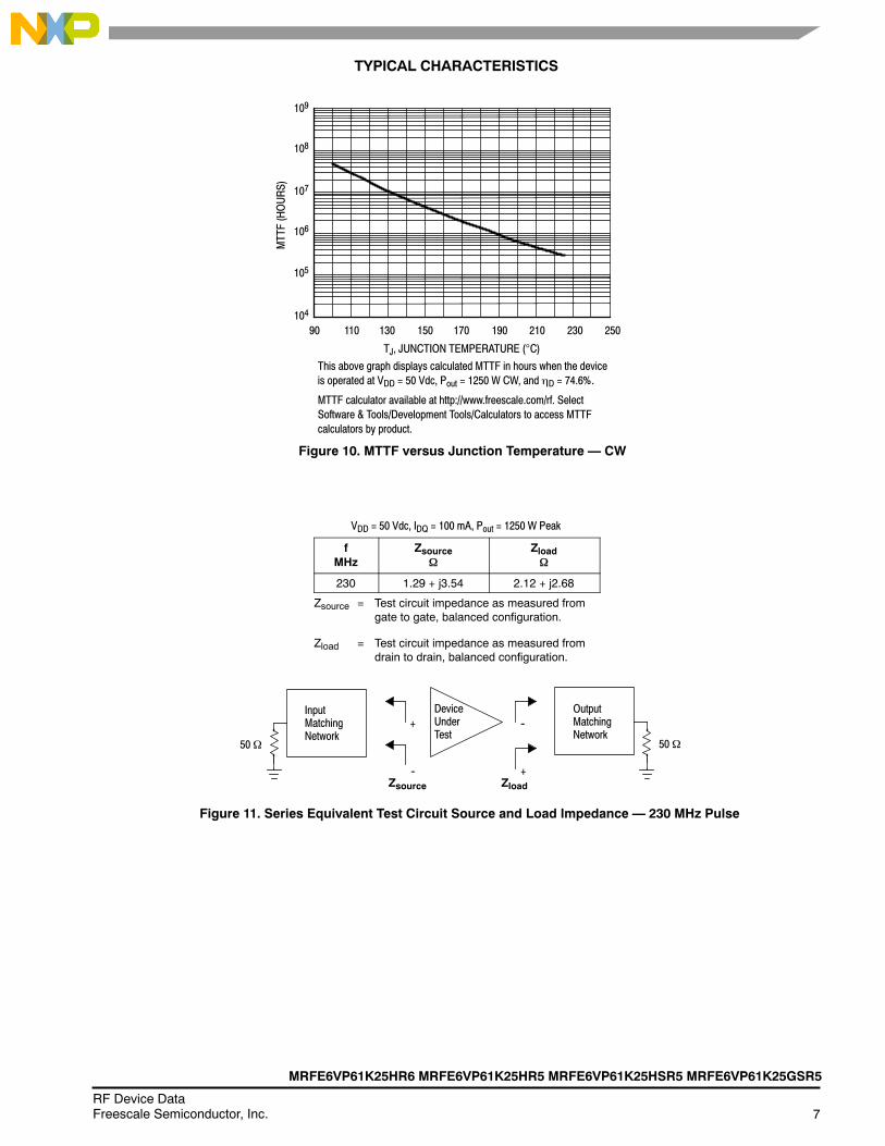
250
109
90
TJ, JUNCTION TEMPERATURE (C)
Figure 10. MTTF versus Junction Temperature — CW
This above graph displays calculated MTTF in hours when the deviceis operated at VDD = 50 Vdc, Pout = 1250 W CW, and D = 74.6%.
MTTF calculator available at http://www.freescale.com/rf. SelectSoftware & Tools/Development Tools/Calculators to access MTTFcalculators by product.
107
106
104
110 130 150 170 190
MTTF(HOURS)
210 230
108
105
VDD = 50 Vdc, IDQ = 100 mA, Pout = 1250 W Peak
fMHz
Zsource
Zload
230 1.29 + j3.54 2.12 + j2.68
Zsource = Test circuit impedance as measured fromgate to gate, balanced configuration.
Zload = Test circuit impedance as measured fromdrain to drain, balanced configuration.
InputMatchingNetwork
DeviceUnderTest
OutputMatchingNetwork
--
-- +
+
Zsource Zload
Figure 11. Series Equivalent Test Circuit Source and Load Impedance — 230 MHz Pulse
5050

8RF Device Data
Freescale Semiconductor, Inc.
MRFE6VP61K25HR6 MRFE6VP61K25HR5 MRFE6VP61K25HSR5 MRFE6VP61K25GSR5
VDD = 50 Vdc, IDQ = 100 mA
f(MHz)
Zsource()
Zload()
1.8 (1) 34.4 + j192.0 (1) 5.00 - j4.00 (1)
27 12.5 + j7.00 7.00 + j0.70
40 5.75 + j5.06 5.39 + j2.62
81.36 4.04 + j5.93 4.89 + j2.95
88 2.20 + j6.70 4.90 + j2.90
98 2.30 + j6.90 4.10 + j2.50
108 2.30 + j7.00 4.40 + j3.60
144 1.60 + j5.00 3.90 + j1.50
175 1.33 + j3.90 3.50 + j2.50
230 1.29 + j3.54 2.12 + j2.68
352 0.98 + j1.45 1.82 + j2.05
500 0.29 + j1.47 1.79 + j1.80
1. Simulated data.
Zsource = Test circuit impedance as measured fromgate to gate, balanced configuration.
Zload = Test circuit impedance as measured fromdrain to drain, balanced configuration.
InputMatchingNetwork
DeviceUnderTest
OutputMatchingNetwork
--
-- +
+
Zsource Zload
5050
Figure 12. Source and Load Impedances Optimized for IRL, Power and Efficiency — Push--Pull
MRFE6VP61K25HR6 MRFE6VP61K25HR5 MRFE6VP61K25HSR5 MRFE6VP61K25GSR5
9RF Device DataFreescale Semiconductor, Inc.
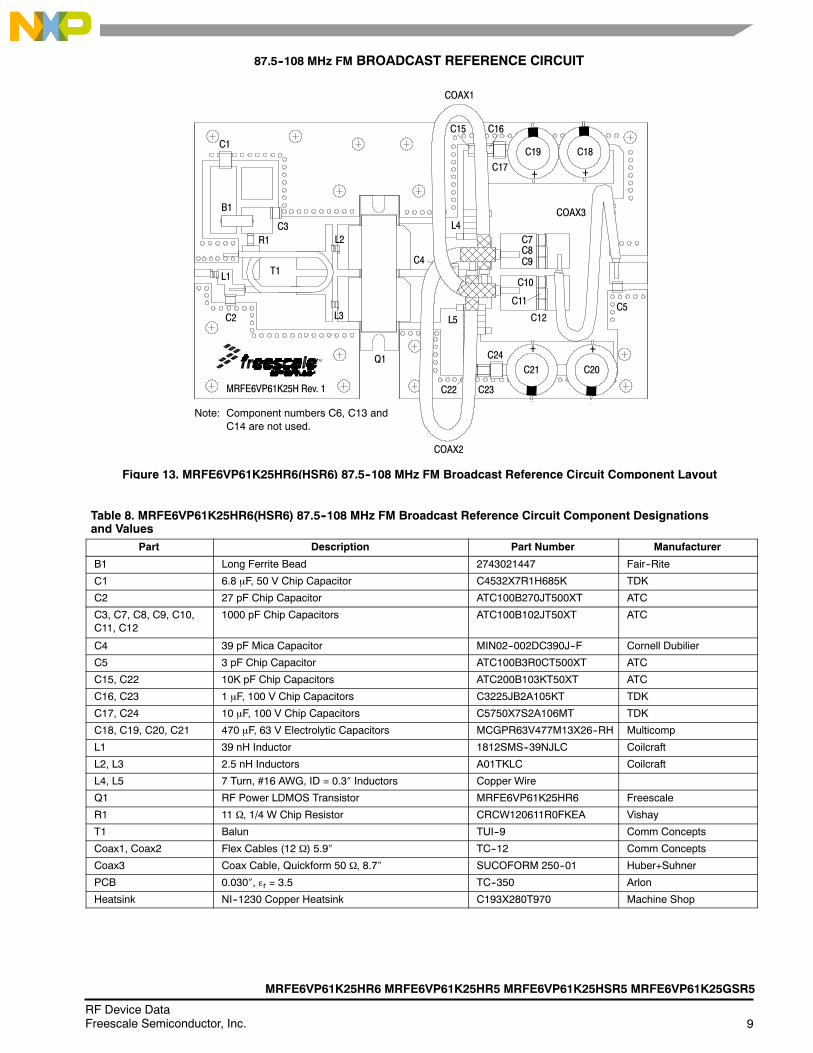
87.5--108 MHz FM BROADCAST REFERENCE CIRCUIT
Figure 13. MRFE6VP61K25HR6(HSR6) 87.5--108 MHz FM Broadcast Reference Circuit Component Layout
+ +
+ +
L2
L3
C3R1
B1
C1
L1
C2
T1
COAX1
COAX2
C22 C23
C24C21 C20
C19 C18
C15 C16
C17
L4
L5
C7C8C9
C10
C12
C11 C5
C4
COAX3
MRFE6VP61K25H Rev. 1
Note: Component numbers C6, C13 andC14 are not used.
Q1
Table 8. MRFE6VP61K25HR6(HSR6) 87.5--108 MHz FM Broadcast Reference Circuit Component Designationsand Values
Part Description Part Number Manufacturer
B1 Long Ferrite Bead 2743021447 Fair--Rite
C1 6.8 F, 50 V Chip Capacitor C4532X7R1H685K TDK
C2 27 pF Chip Capacitor ATC100B270JT500XT ATC
C3, C7, C8, C9, C10,C11, C12
1000 pF Chip Capacitors ATC100B102JT50XT ATC
C4 39 pF Mica Capacitor MIN02--002DC390J--F Cornell Dubilier
C5 3 pF Chip Capacitor ATC100B3R0CT500XT ATC
C15, C22 10K pF Chip Capacitors ATC200B103KT50XT ATC
C16, C23 1 F, 100 V Chip Capacitors C3225JB2A105KT TDK
C17, C24 10 F, 100 V Chip Capacitors C5750X7S2A106MT TDK
C18, C19, C20, C21 470 F, 63 V Electrolytic Capacitors MCGPR63V477M13X26--RH Multicomp
L1 39 nH Inductor 1812SMS--39NJLC Coilcraft
L2, L3 2.5 nH Inductors A01TKLC Coilcraft
L4, L5 7 Turn, #16 AWG, ID = 0.3 Inductors Copper Wire
Q1 RF Power LDMOS Transistor MRFE6VP61K25HR6 Freescale
R1 11 , 1/4 W Chip Resistor CRCW120611R0FKEA Vishay
T1 Balun TUI--9 Comm Concepts
Coax1, Coax2 Flex Cables (12 ) 5.9 TC--12 Comm Concepts
Coax3 Coax Cable, Quickform 50 , 8.7 SUCOFORM 250--01 Huber+Suhner
PCB 0.030, r = 3.5 TC--350 Arlon
Heatsink NI--1230 Copper Heatsink C193X280T970 Machine Shop
10RF Device Data
Freescale Semiconductor, Inc.
MRFE6VP61K25HR6 MRFE6VP61K25HR5 MRFE6VP61K25HSR5 MRFE6VP61K25GSR5
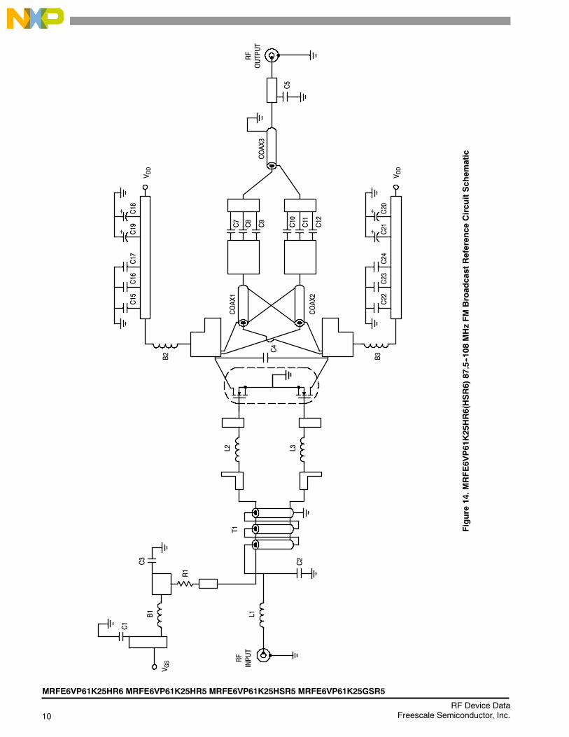
RF
INPUT
V GS
RF
OUTPUT
C1
B1 L1
R1
C3
C2
T1L2 L3
B2 B3
C4
C15
C16
C17
C19
C18
C22
C23
C24
C21
C20
COAX1
COAX2
C7
C8
C9
C10
C11
C12
C5
COAX3
V DD
V DD
Figure
14.M
RFE6V
P61K25HR6(HSR6)87.5--108
MHzFMBroadcastReference
CircuitSchem
atic
+
+
+
+
MRFE6VP61K25HR6 MRFE6VP61K25HR5 MRFE6VP61K25HSR5 MRFE6VP61K25GSR5
11RF Device DataFreescale Semiconductor, Inc.
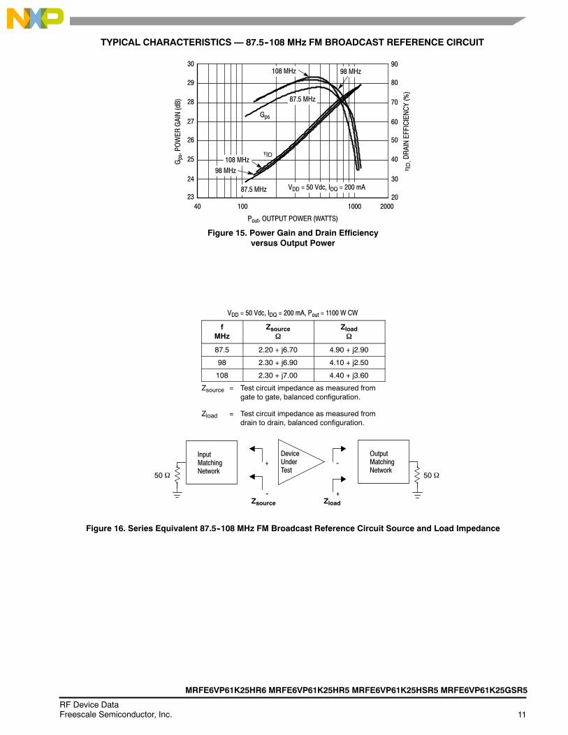
TYPICAL CHARACTERISTICS — 87.5--108 MHz FM BROADCAST REFERENCE CIRCUIT
30
20
90
40
28 70
50
Pout, OUTPUT POWER (WATTS)
Figure 15. Power Gain and Drain Efficiencyversus Output Power
Gps,POWER
GAIN(dB)
D,DRAINEFFICIENCY(%)
26
232000
25 40
60
80
27
29
1000
D
Gps
VDD = 50 Vdc, IDQ = 200 mA24 30
100
108 MHz 98 MHz
87.5 MHz
108 MHz98 MHz
87.5 MHz
VDD = 50 Vdc, IDQ = 200 mA, Pout = 1100 W CW
fMHz
Zsource
Zload
87.5 2.20 + j6.70 4.90 + j2.90
98 2.30 + j6.90 4.10 + j2.50
108 2.30 + j7.00 4.40 + j3.60
Zsource = Test circuit impedance as measured fromgate to gate, balanced configuration.
Zload = Test circuit impedance as measured fromdrain to drain, balanced configuration.
Figure 16. Series Equivalent 87.5--108 MHz FM Broadcast Reference Circuit Source and Load Impedance
InputMatchingNetwork
DeviceUnderTest
OutputMatchingNetwork
--
-- +
+
Zsource Zload
50 50
12RF Device Data
Freescale Semiconductor, Inc.
MRFE6VP61K25HR6 MRFE6VP61K25HR5 MRFE6VP61K25HSR5 MRFE6VP61K25GSR5
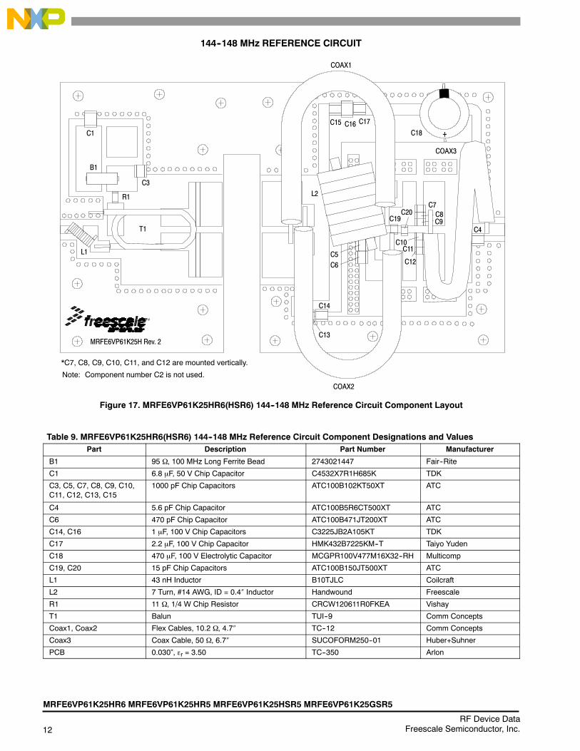
144--148 MHz REFERENCE CIRCUIT
Figure 17. MRFE6VP61K25HR6(HSR6) 144--148 MHz Reference Circuit Component Layout
+C1
COAX1
MRFE6VP61K25H Rev. 2
C3
R1
B1
L1
T1
C13
C14
COAX2
COAX3
C6C5
C19C20
C7C8C9
C10C11
C12
C4
C18C15 C16 C17
L2
*C7, C8, C9, C10, C11, and C12 are mounted vertically.
Note: Component number C2 is not used.
Table 9. MRFE6VP61K25HR6(HSR6) 144--148 MHz Reference Circuit Component Designations and ValuesPart Description Part Number Manufacturer
B1 95 , 100 MHz Long Ferrite Bead 2743021447 Fair--Rite
C1 6.8 F, 50 V Chip Capacitor C4532X7R1H685K TDK
C3, C5, C7, C8, C9, C10,C11, C12, C13, C15
1000 pF Chip Capacitors ATC100B102KT50XT ATC
C4 5.6 pF Chip Capacitor ATC100B5R6CT500XT ATC
C6 470 pF Chip Capacitor ATC100B471JT200XT ATC
C14, C16 1 F, 100 V Chip Capacitors C3225JB2A105KT TDK
C17 2.2 F, 100 V Chip Capacitor HMK432B7225KM--T Taiyo Yuden
C18 470 F, 100 V Electrolytic Capacitor MCGPR100V477M16X32--RH Multicomp
C19, C20 15 pF Chip Capacitors ATC100B150JT500XT ATC
L1 43 nH Inductor B10TJLC Coilcraft
L2 7 Turn, #14 AWG, ID = 0.4 Inductor Handwound Freescale
R1 11 , 1/4 W Chip Resistor CRCW120611R0FKEA Vishay
T1 Balun TUI--9 Comm Concepts
Coax1, Coax2 Flex Cables, 10.2 , 4.7 TC--12 Comm Concepts
Coax3 Coax Cable, 50 , 6.7 SUCOFORM250--01 Huber+Suhner
PCB 0.030”, r = 3.50 TC--350 Arlon
MRFE6VP61K25HR6 MRFE6VP61K25HR5 MRFE6VP61K25HSR5 MRFE6VP61K25GSR5
13RF Device DataFreescale Semiconductor, Inc.
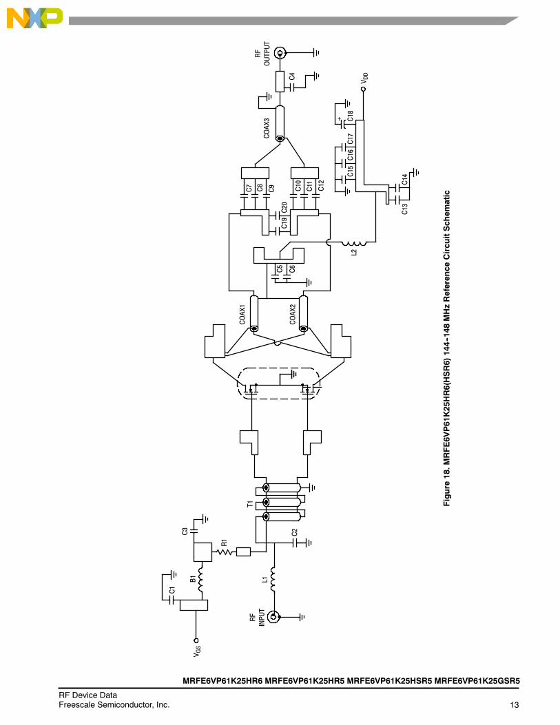
Figure
18.M
RFE6V
P61K25HR6(HSR6)144--148
MHzReference
CircuitSchem
atic
C7 C8
C9 C10
C11 C12
RF
OUTPUT
C4
COAX1
COAX2
COAX3
C5
C6
C19
C20
C17
C16
C15
C18
V DD
C13
C14
L2
B1
C1
V GS
C3
R1
C2
L1
RF
INPUT
T1
+

14RF Device Data
Freescale Semiconductor, Inc.
MRFE6VP61K25HR6 MRFE6VP61K25HR5 MRFE6VP61K25HSR5 MRFE6VP61K25GSR5
TYPICAL CHARACTERISTICS — 144--148 MHz REFERENCE CIRCUIT
VDD = 50 Vdc, IDQ = 200 mA, Pout = 1100 W CW
fMHz
Zsource
Zload
144 1.6 + j5.0 3.9 + j1.5
Zsource = Test circuit impedance as measured fromgate to gate, balanced configuration.
Zload = Test circuit impedance as measured fromdrain to drain, balanced configuration.
Figure 19. Series Equivalent 144--148 MHz Reference Circuit Source and Load Impedance
InputMatchingNetwork
DeviceUnderTest
OutputMatchingNetwork
--
-- +
+
Zsource Zload
50 50
31
20
90
50
28
70
50
Pout, OUTPUT POWER (WATTS)
Figure 20. Power Gain and Drain Efficiencyversus Output Power
Gps,POWER
GAIN(dB)
D,DRAINEFFICIENCY(%)
26
242000
25
40
60
80
27
29
1000
D
VDD = 50 Vdc, IDQ = 2500 mA, f = 144 MHz
30
100
30
1
Pout, OUTPUT POWER (WATTS) PEP
Figure 21. Intermodulation Distortion Productsversus Output Power
--100
0
--20
IMD,INTERMODULATIONDISTORTION(dBc)
--50
--60
--70
--80
--90
--30
--40IDQ = 2500 mA
10 1000
--20
100 2000
VDD = 50 Vdcf1 = 143.9 MHz, f2 = 144.1 MHzTwo--Tone Measurement
3rd Order
3rd Order
7th Order
7th Order
5th Order
4500 mA
4500 mA
Gps
MRFE6VP61K25HR6 MRFE6VP61K25HR5 MRFE6VP61K25HSR5 MRFE6VP61K25GSR5
15RF Device DataFreescale Semiconductor, Inc.
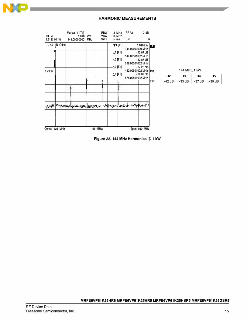
HARMONIC MEASUREMENTS
Figure 22. 144 MHz Harmonics @ 1 kW
H2 H3 H4 H5
--42 dB --33 dB --37 dB --39 dB
144 MHz, 1 kW
1.018 kW144.00000000 MHz
--42.07 dB144.00501002 MHz
--32.87 dB288.00501002 MHz
--37.26 dB432.00501002 MHz
--38.89 dB576.00501002 MHz
B1 [T1]
1 [T1]
2 [T1]
3 [T1]
4 [T1]
1
23
4
1
Ref Lvl1.5 E 04 W
Marker 1 [T1]1.018
144.00000000
RBWVBWSWT
3 MHz3 MHz5 ms
RF Att
Unit
10 dB
W
77.7 dB Offset
1 VIEW 1SA
EXT
kWMHz
Center 525 MHz 95 MHz/ Span 950 MHz
A

16RF Device Data
Freescale Semiconductor, Inc.
MRFE6VP61K25HR6 MRFE6VP61K25HR5 MRFE6VP61K25HSR5 MRFE6VP61K25GSR5
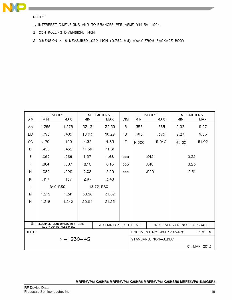
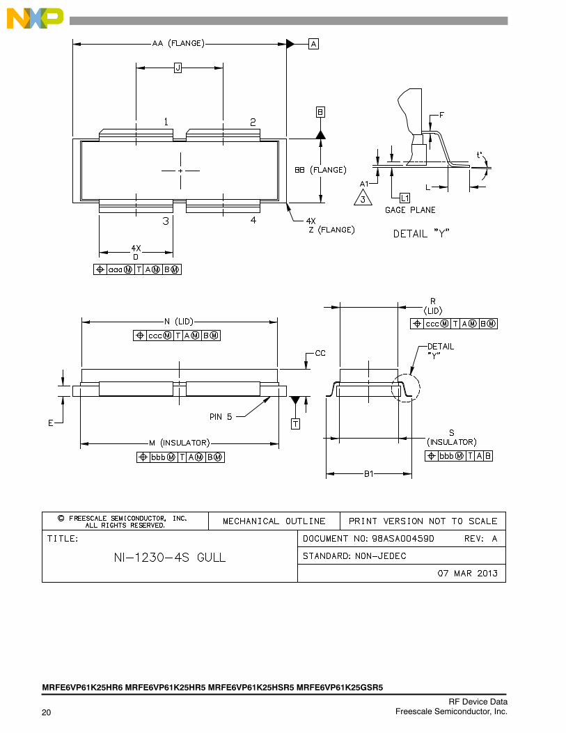
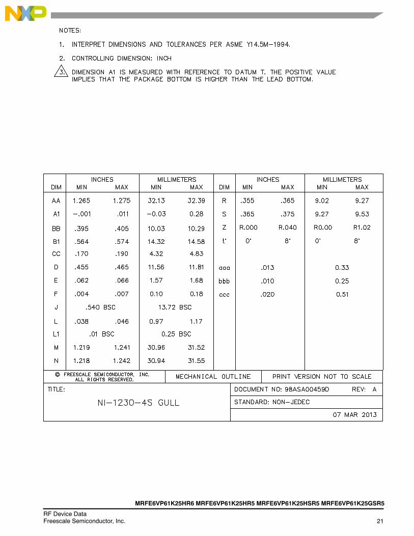
PACKAGE DIMENSIONS
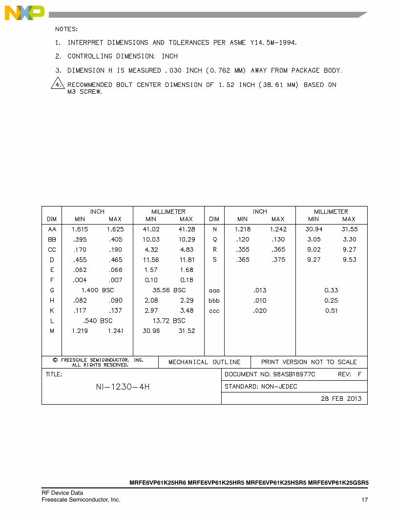
MRFE6VP61K25HR6 MRFE6VP61K25HR5 MRFE6VP61K25HSR5 MRFE6VP61K25GSR5
17RF Device DataFreescale Semiconductor, Inc.

18RF Device Data
Freescale Semiconductor, Inc.
MRFE6VP61K25HR6 MRFE6VP61K25HR5 MRFE6VP61K25HSR5 MRFE6VP61K25GSR5
MRFE6VP61K25HR6 MRFE6VP61K25HR5 MRFE6VP61K25HSR5 MRFE6VP61K25GSR5
19RF Device DataFreescale Semiconductor, Inc.
20RF Device Data
Freescale Semiconductor, Inc.
MRFE6VP61K25HR6 MRFE6VP61K25HR5 MRFE6VP61K25HSR5 MRFE6VP61K25GSR5
MRFE6VP61K25HR6 MRFE6VP61K25HR5 MRFE6VP61K25HSR5 MRFE6VP61K25GSR5
21RF Device DataFreescale Semiconductor, Inc.
22RF Device Data
Freescale Semiconductor, Inc.
MRFE6VP61K25HR6 MRFE6VP61K25HR5 MRFE6VP61K25HSR5 MRFE6VP61K25GSR5
PRODUCT DOCUMENTATION AND SOFTWARE
Refer to the following documents and software to aid your design process.
Application Notes
AN1955: Thermal Measurement Methodology of RF Power AmplifiersEngineering Bulletins
EB212: Using Data Sheet Impedances for RF LDMOS DevicesSoftware
Electromigration MTTF Calculator RF High Power Model .s2p File
For Software, do a Part Number search at http://www.freescale.com, and select the “Part Number” link. Go to theSoftware & Tools tab on the part’s Product Summary page to download the respective tool.
REVISION HISTORYThe following table summarizes revisions to this document.
Revision Date Description
0 Nov. 2010 Initial Release of Data Sheet
1 Jan. 2011 Fig. 1, Pin Connections, corrected pin 4 label from RFout/VGS to RFin/VGS, p. 1
2 May 2012 Added Application Circuits Typical Performance table, p. 1 Capable of Handling VSWR bullet: corrected 1250 Peak Output Power value to 1500 and converted to table,
pp. 1, 3 Table 1, Max Ratings: final DC test specification for Drain--Source Voltage changed from +125 to +133 Vdc,
p. 2 Table 3, ESD Protection Characteristics: added the device’s ESD passing level as applicable to each ESD
class, p. 2 Table 4, Off Characteristics: final DC test specification for Drain--Source Breakdown Voltage minimum value
changed from 125 to 133 Vdc, p. 2 Table 4, On Characteristics: added Forward Transconductance, p. 2 Fig. 10, MTTF versus Junction Temperature -- CW: MTTF end temperature on graph changed to match
maximum operating junction temperature, p. 7 Added Fig. 12, Source and Load Impedances Optimized for IRL, Power and Efficiency — Push--pull, p. 8 Added Fig. 13, 87.5--108 MHz FM Broadcast Reference Circuit Component Layout, p. 9 Added Table 9, 87.5--108 MHz FM Broadcast Reference Circuit Component Designations and Values, p. 9 Added Fig. 14, 87.5--108 MHz FM Broadband Reference Circuit Schematic, p. 10 Added Fig. 15, Power Gain and Drain Efficiency versus Output Power (87.5--108 MHz), p. 11 Added Fig. 16, Series Equivalent 87.5--108 MHz FM Broadcast Reference Circuit Source and Load
Impedance, p. 11 Added Fig. 17, 144--148 MHz Reference Circuit Component Layout, p. 12 Added Table 9, 144--148 MHz Reference Circuit Component Designations and Values, p. 12 Added Fig. 18, 144--148 MHz Reference Circuit Schematic, p. 13 Added Fig. 19, Series Equivalent 144--148 MHz Reference Circuit Source and Load Impedance, p. 14 Added Fig. 20, Power Gain and Drain Efficiency versus Output Power (144--148 MHz), p. 14 Added Fig. 21, Intermodulation Distortion Products versus Output Power (144--148 MHz), p. 14 Added Fig. 22, 144 MHz Harmonics @ 1 kW, p. 15
3 Oct. 2012 Added part number MRFE6VP61K25GSR5, p. 1 Added 2282--02 (NI--1230S--4 Gull) package isometric, p. 1, and Mechanical Outline, p. 20, 21
4 Mar. 2013 MRFE6VP61K25HR6 tape and reel option replaced with MRF6VP61K25HR5 per PCN15551. Replaced Case Outline 98ASB16977C, Issue E with Issue F, p. 16, 17. Changed dimension C from
0.150--0.200 to CC 0.170--0.190. Replaced Case Outline 98ARB18247C, Issue F with Issue G, p. 18, 19. Changed dimension C from
0.150--0.200 to CC 0.170--0.190. Added minimum Z dimension R0.00. Replaced Case Outline 98ASA00459D, Issue O with Issue A, p. 20, 21. Changed dimension C from
0.150--0.200 to CC 0.170--0.190. Corrected positional tolerance for dimension S.
4.1 Mar. 2014 MRFE6VP61K25HR5 part added to data sheet device box, p. 1 MRFE6VP61K25HSR6 tape and reel option replaced with MRFE6VP61K25HSR5 per PCN15551. (Note: this
copy updates the copy from Rev. 4 Revision History to accurately reflect the part number replacement in thisdata sheet as described in PCN15551.)

MRFE6VP61K25HR6 MRFE6VP61K25HR5 MRFE6VP61K25HSR5 MRFE6VP61K25GSR5
23RF Device DataFreescale Semiconductor, Inc.
Information in this document is provided solely to enable system and softwareimplementers to use Freescale products. There are no express or implied copyrightlicenses granted hereunder to design or fabricate any integrated circuits based on theinformation in this document.
Freescale reserves the right to make changes without further notice to any productsherein. Freescale makes no warranty, representation, or guarantee regarding thesuitability of its products for any particular purpose, nor does Freescale assume anyliability arising out of the application or use of any product or circuit, and specificallydisclaims any and all liability, including without limitation consequential or incidentaldamages. “Typical” parameters that may be provided in Freescale data sheets and/orspecifications can and do vary in different applications, and actual performance mayvary over time. All operating parameters, including “typicals,” must be validated foreach customer application by customer’s technical experts. Freescale does not conveyany license under its patent rights nor the rights of others. Freescale sells productspursuant to standard terms and conditions of sale, which can be found at the followingaddress: freescale.com/SalesTermsandConditions.
Freescale and the Freescale logo are trademarks of Freescale Semiconductor, Inc.,Reg. U.S. Pat. & Tm. Off. All other product or service names are the property of theirrespective owners.E 2014 Freescale Semiconductor, Inc.
How to Reach Us:
Home Page:freescale.com
Web Support:freescale.com/support
Document Number: MRFE6VP61K25HRev. 4.1, 3/2014