Document Number: MRFE6VP5600H Technical Data Rev. 1, 1...
13
RF Power Field Effect Transistors High Ruggedness N--Channel Enhancement--Mode Lateral MOSFETs These high ruggedness devices are designed for use in high VSWR industrial (including laser and plasma exciters), broadcast (analog and digital), aerospace and radio/land mobile applications. They are unmatched input and output designs allowing wide frequency range utilization, between 1.8 and 600 MHz. • Typical Performance: V DD = 50 Volts, I DQ = 100 mA Signal Type P out (W) f (MHz) G ps (dB) η D (%) IRL (dB) Pulsed (100 μsec, 20% Duty Cycle) 600 Peak 230 25.0 74.6 --18 CW 600 Avg. 230 24.6 75.2 --17 • Capable of Handling a Load Mismatch of 65:1 VSWR, @ 50 Vdc, 230 MHz, at all Phase Angles, Designed for Enhanced Ruggedness • 600 Watts Pulsed Peak Power, 20% Duty Cycle, 100 μsec Features • Unmatched Input and Output Allowing Wide Frequency Range Utilization • Device can be used Single--Ended or in a Push--Pull Configuration • Qualified Up to a Maximum of 50 V DD Operation • Characterized from 30 V to 50 V for Extended Power Range • Suitable for Linear Application with Appropriate Biasing • Integrated ESD Protection with Greater Negative Gate--Source Voltage Range for Improved Class C Operation • Characterized with Series Equivalent Large--Signal Impedance Parameters • RoHS Compliant • In Tape and Reel. R6 Suffix = 150 Units, 56 mm Tape Width, 13 inch Reel. For R5 Tape and Reel options, see p. 12. Table 1. Maximum Ratings Rating Symbol Value Unit Drain--Source Voltage V DSS --0.5, +130 Vdc Gate--Source Voltage V GS --6.0, +10 Vdc Storage Temperature Range T stg --65 to +150 °C Case Operating Temperature T C 150 °C Total Device Dissipation @ T C = 25°C Derate above 25°C P D 1667 8.33 W W/°C Operating Junction Temperature (1,2) T J 225 °C Table 2. Thermal Characteristics Characteristic Symbol Value (2,3) Unit Thermal Resistance, Junction to Case Case Temperature 68°C, 600 W Pulsed, 100 μsec Pulse Width, 20% Duty Cycle, 100 mA, 230 MHz Case Temperature 60°C, 600 W CW, 100 mA, 230 MHz Z θJC R θJC 0.022 0.12 °C/W 1. Continuous use at maximum temperature will affect MTTF. 2. MTTF calculator available at http://www.freescale.com/rf . Select Software & Tools/Development Tools/Calculators to access MTTF calculators by product. 3. Refer to AN1955, Thermal Measurement Methodology of RF Power Amplifiers. Go to http://www.freescale.com/rf . Select Documentation/Application Notes -- AN1955. Document Number: MRFE6VP5600H Rev. 1, 1/2011 Freescale Semiconductor Technical Data 1.8--600 MHz, 600 W CW, 50 V LATERAL N--CHANNEL BROADBAND RF POWER MOSFETs MRFE6VP5600HR6 MRFE6VP5600HSR6 (Top View) RF out /V DS 3 1 Figure 1. Pin Connections 4 2 RF out /V DS RF in /V GS RF in /V GS CASE 375D--05, STYLE 1 NI--1230 MRFE6VP5600HR6 CASE 375E--04, STYLE 1 NI--1230S MRFE6VP5600HSR6 PARTS ARE PUSH--PULL © Freescale Semiconductor, Inc., 2010--2011. All rights reserved.
Transcript of Document Number: MRFE6VP5600H Technical Data Rev. 1, 1...

MRFE6VP5600HR6 MRFE6VP5600HSR6
1RF Device DataFreescale Semiconductor
RF Power Field Effect TransistorsHigh Ruggedness N--ChannelEnhancement--Mode Lateral MOSFETsThese high ruggedness devices are designed for use in high VSWR industrial
(including laser and plasma exciters), broadcast (analog and digital), aerospaceand radio/land mobile applications. They are unmatched input and outputdesigns allowing wide frequency range utilization, between 1.8 and 600 MHz.
• Typical Performance: VDD = 50 Volts, IDQ = 100 mA
Signal TypePout(W)
f(MHz)
Gps(dB)
ηD(%)
IRL(dB)
Pulsed (100 μsec,20% Duty Cycle)
600 Peak 230 25.0 74.6 --18
CW 600 Avg. 230 24.6 75.2 --17
• Capable of Handling a Load Mismatch of 65:1 VSWR, @ 50 Vdc,230 MHz, at all Phase Angles, Designed for Enhanced Ruggedness• 600 Watts Pulsed Peak Power, 20% Duty Cycle, 100 μsec
Features• Unmatched Input and Output Allowing Wide Frequency Range Utilization
• Device can be used Single--Ended or in a Push--Pull Configuration
• Qualified Up to a Maximum of 50 VDD Operation• Characterized from 30 V to 50 V for Extended Power Range• Suitable for Linear Application with Appropriate Biasing• Integrated ESD Protection with Greater Negative Gate--Source Voltage
Range for Improved Class C Operation• Characterized with Series Equivalent Large--Signal Impedance Parameters
• RoHS Compliant• In Tape and Reel. R6 Suffix = 150 Units, 56 mm Tape Width, 13 inch Reel.
For R5 Tape and Reel options, see p. 12.
Table 1. Maximum Ratings
Rating Symbol Value Unit
Drain--Source Voltage VDSS --0.5, +130 Vdc
Gate--Source Voltage VGS --6.0, +10 Vdc
Storage Temperature Range Tstg -- 65 to +150 °C
Case Operating Temperature TC 150 °C
Total Device Dissipation @ TC = 25°CDerate above 25°C
PD 16678.33
WW/°C
Operating Junction Temperature (1,2) TJ 225 °C
Table 2. Thermal Characteristics
Characteristic Symbol Value (2,3) Unit
Thermal Resistance, Junction to CaseCase Temperature 68°C, 600 W Pulsed, 100 μsec Pulse Width, 20% Duty Cycle, 100 mA, 230 MHzCase Temperature 60°C, 600 W CW, 100 mA, 230 MHz
ZθJCRθJC
0.0220.12
°C/W
1. Continuous use at maximum temperature will affect MTTF.2. MTTF calculator available at http://www.freescale.com/rf. Select Software & Tools/Development Tools/Calculators to access
MTTF calculators by product.3. Refer to AN1955, Thermal Measurement Methodology of RF Power Amplifiers. Go to http://www.freescale.com/rf.
Select Documentation/Application Notes -- AN1955.
Document Number: MRFE6VP5600HRev. 1, 1/2011
Freescale SemiconductorTechnical Data
1.8--600 MHz, 600 W CW, 50 VLATERAL N--CHANNEL
BROADBANDRF POWER MOSFETs
MRFE6VP5600HR6MRFE6VP5600HSR6
(Top View)
RFout/VDS3 1
Figure 1. Pin Connections
4 2 RFout/VDS
RFin/VGS
RFin/VGS
CASE 375D--05, STYLE 1NI--1230
MRFE6VP5600HR6
CASE 375E--04, STYLE 1NI--1230S
MRFE6VP5600HSR6
PARTS ARE PUSH--PULL
© Freescale Semiconductor, Inc., 2010--2011. All rights reserved.
2RF Device Data
Freescale Semiconductor
MRFE6VP5600HR6 MRFE6VP5600HSR6
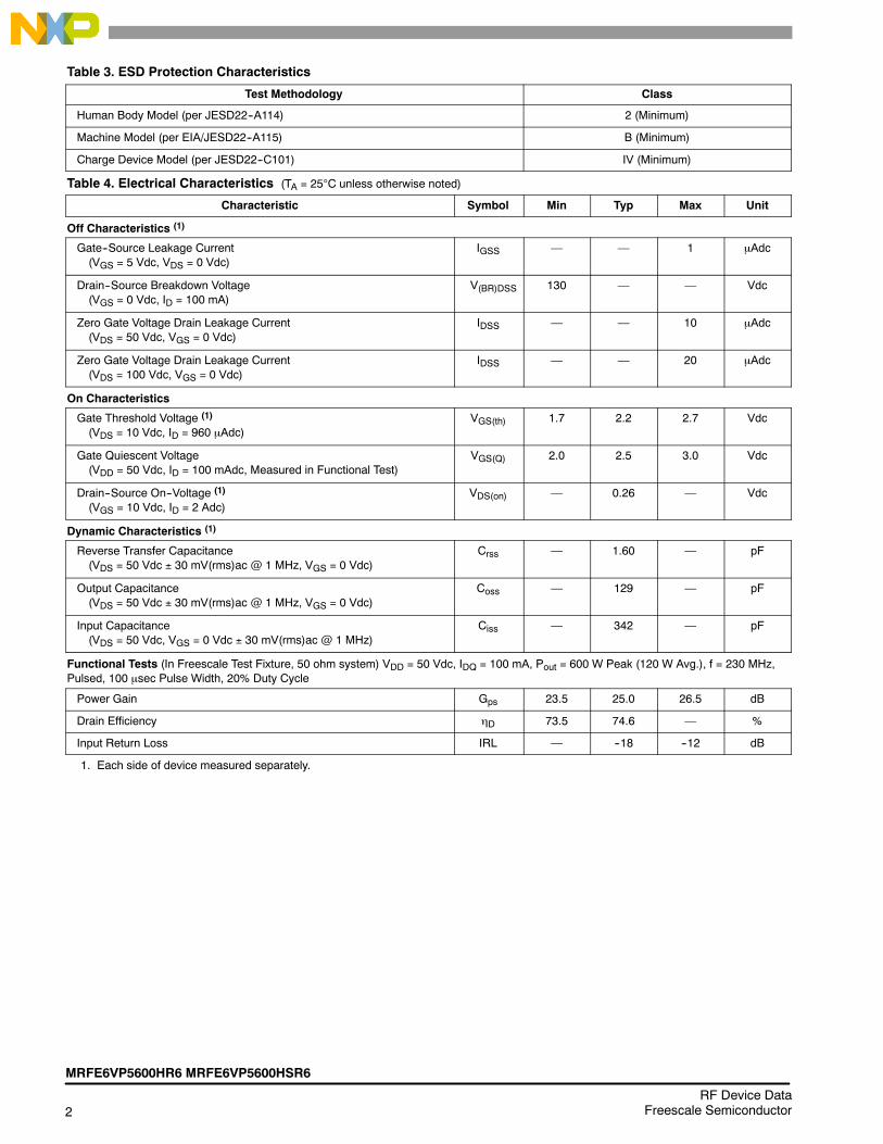
Table 3. ESD Protection Characteristics
Test Methodology Class
Human Body Model (per JESD22--A114) 2 (Minimum)
Machine Model (per EIA/JESD22--A115) B (Minimum)
Charge Device Model (per JESD22--C101) IV (Minimum)
Table 4. Electrical Characteristics (TA = 25°C unless otherwise noted)
Characteristic Symbol Min Typ Max Unit
Off Characteristics (1)
Gate--Source Leakage Current(VGS = 5 Vdc, VDS = 0 Vdc)
IGSS 1 μAdc
Drain--Source Breakdown Voltage(VGS = 0 Vdc, ID = 100 mA)
V(BR)DSS 130 Vdc
Zero Gate Voltage Drain Leakage Current(VDS = 50 Vdc, VGS = 0 Vdc)
IDSS 10 μAdc
Zero Gate Voltage Drain Leakage Current(VDS = 100 Vdc, VGS = 0 Vdc)
IDSS 20 μAdc
On Characteristics
Gate Threshold Voltage (1)
(VDS = 10 Vdc, ID = 960 μAdc)VGS(th) 1.7 2.2 2.7 Vdc
Gate Quiescent Voltage(VDD = 50 Vdc, ID = 100 mAdc, Measured in Functional Test)
VGS(Q) 2.0 2.5 3.0 Vdc
Drain--Source On--Voltage (1)
(VGS = 10 Vdc, ID = 2 Adc)VDS(on) 0.26 Vdc
Dynamic Characteristics (1)
Reverse Transfer Capacitance(VDS = 50 Vdc ± 30 mV(rms)ac @ 1 MHz, VGS = 0 Vdc)
Crss 1.60 pF
Output Capacitance(VDS = 50 Vdc ± 30 mV(rms)ac @ 1 MHz, VGS = 0 Vdc)
Coss 129 pF
Input Capacitance(VDS = 50 Vdc, VGS = 0 Vdc ± 30 mV(rms)ac @ 1 MHz)
Ciss 342 pF
Functional Tests (In Freescale Test Fixture, 50 ohm system) VDD = 50 Vdc, IDQ = 100 mA, Pout = 600 W Peak (120 W Avg.), f = 230 MHz,Pulsed, 100 μsec Pulse Width, 20% Duty Cycle
Power Gain Gps 23.5 25.0 26.5 dB
Drain Efficiency ηD 73.5 74.6 %
Input Return Loss IRL --18 --12 dB
1. Each side of device measured separately.
MRFE6VP5600HR6 MRFE6VP5600HSR6
3RF Device DataFreescale Semiconductor
Figure 1. MRFE6VP5600HR6(HSR6) Test Circuit Schematic -- Pulsed
RFINPUT Z1
DUT
Z16
Z18
Z17
C16
C4
Z23 Z25
COAX1
COAX2
Z27
C10
+
L1
C17
C18
C19
Z28Z26
C15
Z24
C1
Z11
C12C11 C13
Z15 Z21
Z22
C14
VBIAS
VSUPPLY
C23 C24
+
C22 C25
+
L4
Z2
Z3
Z4
C2
C3
Z5
Z6
Z7
Z8C5
Z9
Z10 L2
R1
Z12
R2
C6
+
C8C7 C9
VBIAS
Z13
Z14
Z20
Z19
L3
+
VSUPPLY
C27 C28
+
C26 C29
++
C21
RFOUTPUTZ31
COAX3
COAX4
Z32
C20
Z29
Z30
Z23, Z24 1.251″ x 0.300″ MicrostripZ25, Z26 0.127″ x 0.300″ MicrostripZ27, Z28 0.058″ x 0.300″ MicrostripZ29, Z30 0.058″ x 0.300″ MicrostripZ31 0.186″ x 0.082″ MicrostripZ32 0.179″ x 0.082″ Microstrip
* Line length includes microstrip bends
Z1 0.192″ x 0.082″ MicrostripZ2 0.175″ x 0.082″ MicrostripZ3, Z4 0.170″ x 0.100″ MicrostripZ5, Z6 0.116″ x 0.285″ MicrostripZ7, Z8 0.116″ x 0.285″ MicrostripZ9, Z10 0.108″ x 0.285″ Microstrip
Z11*, Z12* 0.872″ x 0.058″ MicrostripZ13, Z14 0.412″ x 0.726″ MicrostripZ15, Z16 0.371″ x 0.507″ MicrostripZ17*, Z18* 0.466″ x 0.363″ MicrostripZ19*, Z20* 1.187″ x 0.154″ MicrostripZ21, Z22 0.104″ x 0.507″ Microstrip
4RF Device Data
Freescale Semiconductor
MRFE6VP5600HR6 MRFE6VP5600HSR6
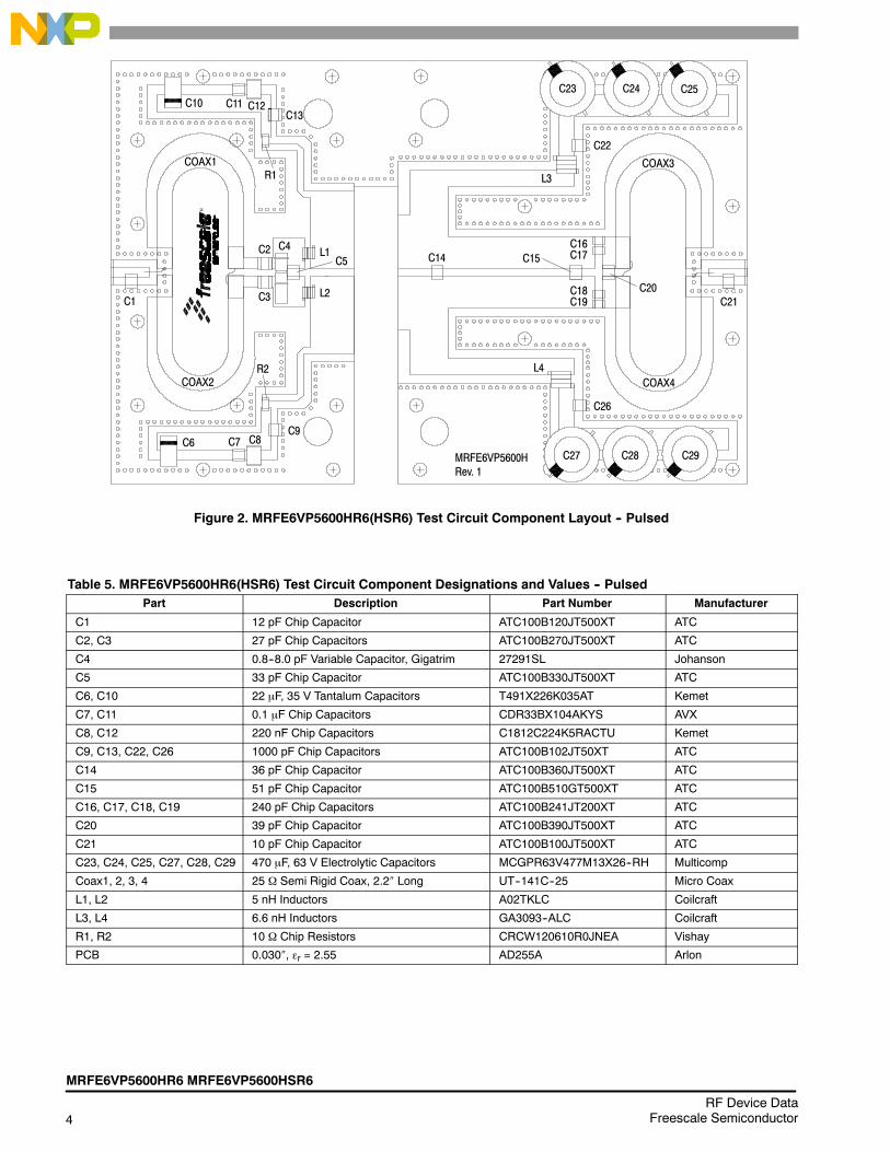
Figure 2. MRFE6VP5600HR6(HSR6) Test Circuit Component Layout -- Pulsed
MRFE6VP5600HRev. 1
COAX2
COAX1
COAX4
COAX3
C10 C11 C12C13
R1
C1
C2
C3
C4 L1
L2
C5 C14
R2
C6 C7 C8C9
C27 C28 C29
C26
L4
C19C18
C15
C21
C17C16
L3
C23 C24 C25
C22
C20
Table 5. MRFE6VP5600HR6(HSR6) Test Circuit Component Designations and Values -- PulsedPart Description Part Number Manufacturer
C1 12 pF Chip Capacitor ATC100B120JT500XT ATC
C2, C3 27 pF Chip Capacitors ATC100B270JT500XT ATC
C4 0.8--8.0 pF Variable Capacitor, Gigatrim 27291SL Johanson
C5 33 pF Chip Capacitor ATC100B330JT500XT ATC
C6, C10 22 μF, 35 V Tantalum Capacitors T491X226K035AT Kemet
C7, C11 0.1 μF Chip Capacitors CDR33BX104AKYS AVX
C8, C12 220 nF Chip Capacitors C1812C224K5RACTU Kemet
C9, C13, C22, C26 1000 pF Chip Capacitors ATC100B102JT50XT ATC
C14 36 pF Chip Capacitor ATC100B360JT500XT ATC
C15 51 pF Chip Capacitor ATC100B510GT500XT ATC
C16, C17, C18, C19 240 pF Chip Capacitors ATC100B241JT200XT ATC
C20 39 pF Chip Capacitor ATC100B390JT500XT ATC
C21 10 pF Chip Capacitor ATC100B100JT500XT ATC
C23, C24, C25, C27, C28, C29 470 μF, 63 V Electrolytic Capacitors MCGPR63V477M13X26--RH Multicomp
Coax1, 2, 3, 4 25 Ω Semi Rigid Coax, 2.2″ Long UT--141C--25 Micro Coax
L1, L2 5 nH Inductors A02TKLC Coilcraft
L3, L4 6.6 nH Inductors GA3093--ALC Coilcraft
R1, R2 10 Ω Chip Resistors CRCW120610R0JNEA Vishay
PCB 0.030″, εr = 2.55 AD255A Arlon
MRFE6VP5600HR6 MRFE6VP5600HSR6
5RF Device DataFreescale Semiconductor
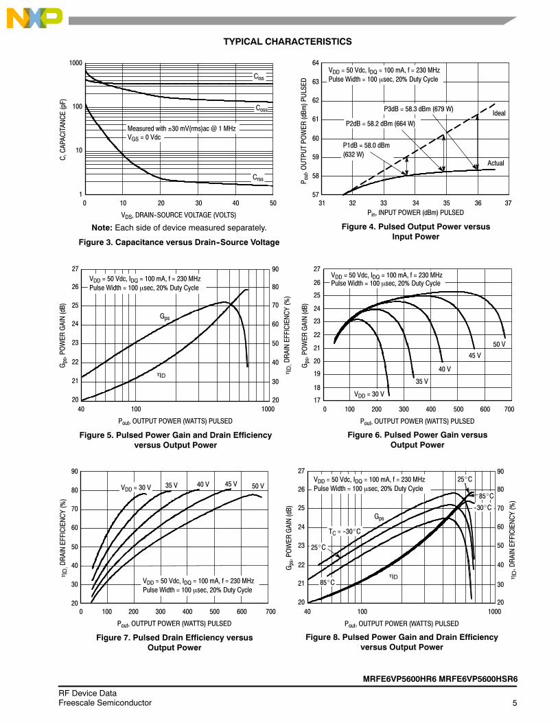
TYPICAL CHARACTERISTICS
50
10
0 2010
VDS, DRAIN--SOURCE VOLTAGE (VOLTS)
Figure 3. Capacitance versus Drain--Source Voltage
C,CAPACITANCE(pF)
30
Ciss
1000
100
40
Measured with ±30 mV(rms)ac @ 1 MHzVGS = 0 Vdc
Note: Each side of device measured separately.
1 57
64
31Pin, INPUT POWER (dBm) PULSED
Figure 4. Pulsed Output Power versusInput Power
62
32 33 34 35 36 37
P out,OUTPUTPOWER
(dBm
)PULSED
61
58
Actual
Ideal
VDD = 50 Vdc, IDQ = 100 mA, f = 230 MHzPulse Width = 100 μsec, 20% Duty Cycle
P1dB = 58.0 dBm(632 W)
60
59
63
P3dB = 58.3 dBm (679 W)
P2dB = 58.2 dBm (664 W)
27
20
90
100
24
70
50
Pout, OUTPUT POWER (WATTS) PULSED
Figure 5. Pulsed Power Gain and Drain Efficiencyversus Output Power
Gps,POWER
GAIN(dB)
ηD,DRAINEFFICIENCY(%)
22
201000
21
40
60
80
23
25
17
24
0
21
20
Pout, OUTPUT POWER (WATTS) PULSED
Figure 6. Pulsed Power Gain versusOutput Power
Gps,POWER
GAIN(dB)
100
19
700
VDD = 50 Vdc, IDQ = 100 mA, f = 230 MHzPulse Width = 100 μsec, 20% Duty Cycle
18
200 400 500 600
VDD = 30 V
50 V22
23
26
25
27
300
35 V
40 V
45 V
20
90
0
Pout, OUTPUT POWER (WATTS) PULSED
Figure 7. Pulsed Drain Efficiency versusOutput Power
70
100 200 300 400 500 600
60
30
50
40
80
700
Figure 8. Pulsed Power Gain and Drain Efficiencyversus Output Power
Pout, OUTPUT POWER (WATTS) PULSED
Gps,POWER
GAIN(dB)
20
22
21
100 1000
ηD
25_C
TC = --30_C
85_C
Gps
VDD = 50 Vdc, IDQ = 100 mA, f = 230 MHzPulse Width = 100 μsec, 20% Duty Cycle
40
60
50
20
30
ηD,DRAINEFFICIENCY(%)85_C
VDD = 50 Vdc, IDQ = 100 mA, f = 230 MHzPulse Width = 100 μsec, 20% Duty Cycle
VDD = 30 V 50 V35 V 40 V 45 V
ηD,DRAINEFFICIENCY(%)
25
24
23
27
26
70
80
90
Crss
ηD
Gps
VDD = 50 Vdc, IDQ = 100 mA, f = 230 MHzPulse Width = 100 μsec, 20% Duty Cycle26
30
40
40
Coss
--30_C
25_C
6RF Device Data
Freescale Semiconductor
MRFE6VP5600HR6 MRFE6VP5600HSR6
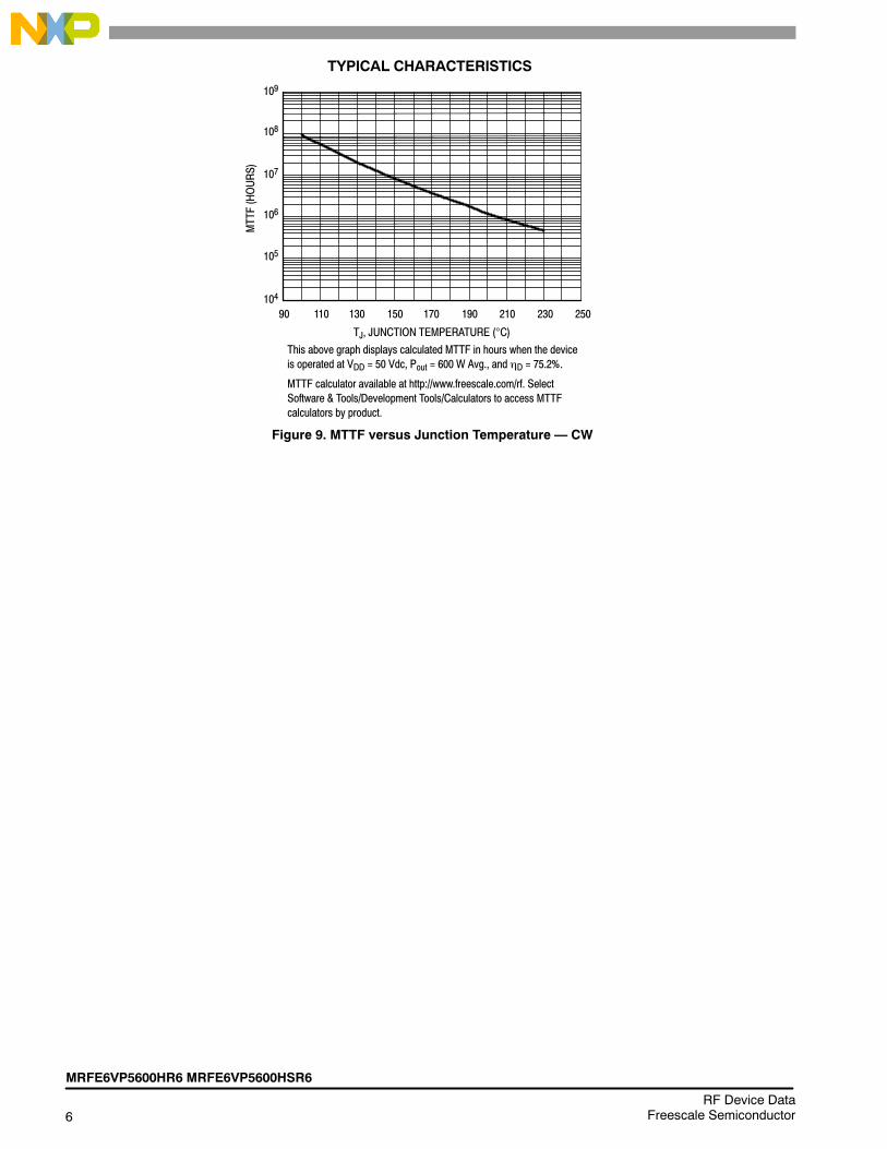
TYPICAL CHARACTERISTICS
250
109
90
TJ, JUNCTION TEMPERATURE (°C)
Figure 9. MTTF versus Junction Temperature CW
This above graph displays calculated MTTF in hours when the deviceis operated at VDD = 50 Vdc, Pout = 600 W Avg., and ηD = 75.2%.
MTTF calculator available at http://www.freescale.com/rf. SelectSoftware & Tools/Development Tools/Calculators to access MTTFcalculators by product.
107
106
104
110 130 150 170 190
MTTF(HOURS)
210 230
108
105
MRFE6VP5600HR6 MRFE6VP5600HSR6
7RF Device DataFreescale Semiconductor
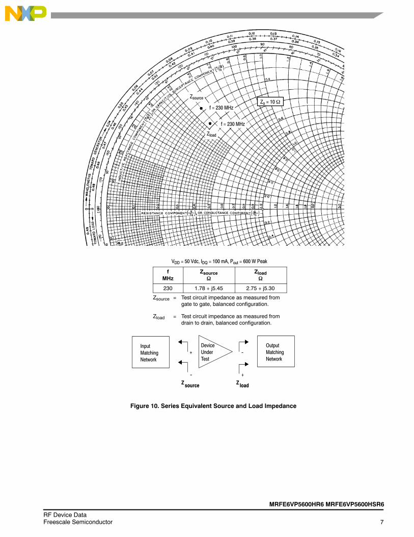
Zo = 10Ω
Zload
Zsource
f = 230 MHz
f = 230 MHz
VDD = 50 Vdc, IDQ = 100 mA, Pout = 600 W Peak
fMHz
ZsourceΩ
ZloadΩ
230 1.78 + j5.45 2.75 + j5.30
Zsource = Test circuit impedance as measured fromgate to gate, balanced configuration.
Zload = Test circuit impedance as measured fromdrain to drain, balanced configuration.
Figure 10. Series Equivalent Source and Load Impedance
Zsource Z load
InputMatchingNetwork
DeviceUnderTest
OutputMatchingNetwork
--
-- +
+
8RF Device Data
Freescale Semiconductor
MRFE6VP5600HR6 MRFE6VP5600HSR6
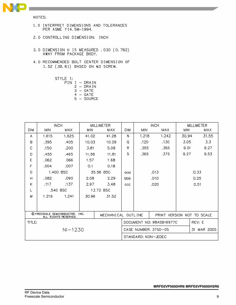
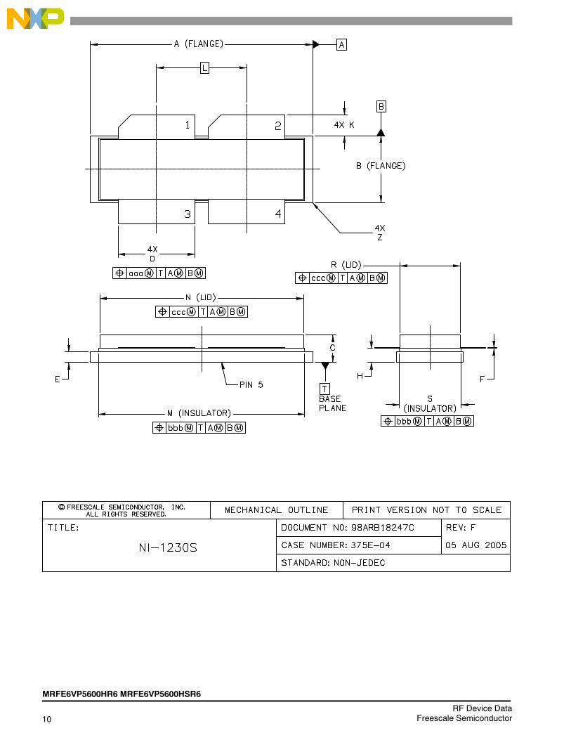
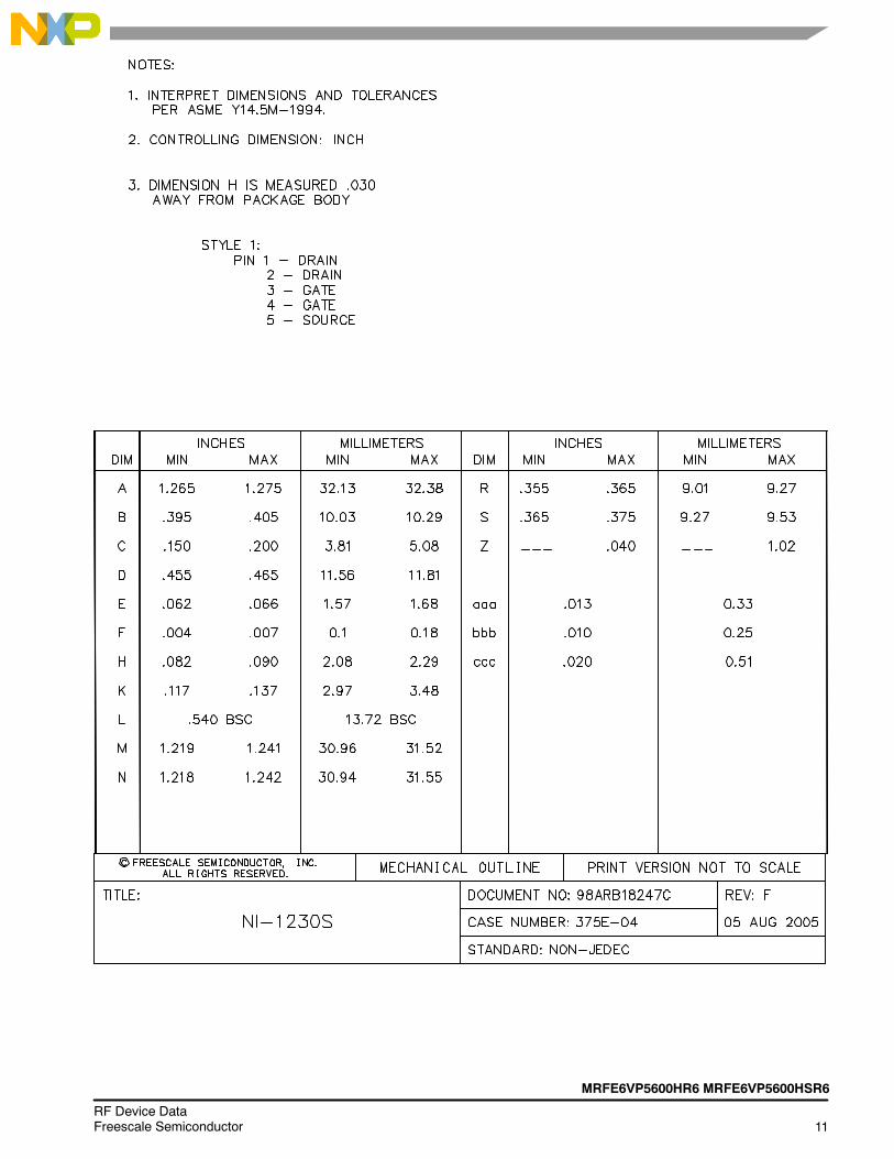
PACKAGE DIMENSIONS
MRFE6VP5600HR6 MRFE6VP5600HSR6
9RF Device DataFreescale Semiconductor
10RF Device Data
Freescale Semiconductor
MRFE6VP5600HR6 MRFE6VP5600HSR6
MRFE6VP5600HR6 MRFE6VP5600HSR6
11RF Device DataFreescale Semiconductor
12RF Device Data
Freescale Semiconductor
MRFE6VP5600HR6 MRFE6VP5600HSR6
PRODUCT DOCUMENTATION AND SOFTWARE
Refer to the following documents and software to aid your design process.
Application Notes• AN1955: Thermal Measurement Methodology of RF Power Amplifiers
Engineering Bulletins• EB212: Using Data Sheet Impedances for RF LDMOS Devices
Software• Electromigration MTTF Calculator
• RF High Power Model
• .s2p File
For Software, do a Part Number search at http://www.freescale.com, and select the Part Number link. Go to the Software &Tools tab on the parts Product Summary page to download the respective tool.
R5 TAPE AND REEL OPTION
R5 Suffix = 50 Units, 56 mm Tape Width, 13 inch Reel.
The R5 tape and reel option for MRFE6VP5600H and MRFE6VP5600HS parts will be available for 2 years after release ofMRFE6VP5600H and MRFE6VP5600HS. Freescale Semiconductor, Inc. reserves the right to limit the quantities that will bedelivered in the R5 tape and reel option. At the end of the 2 year period customers who have purchased these devices in the R5tape and reel option will be offered MRFE6VP5600H and MRFE6VP5600HS in the R6 tape and reel option.
REVISION HISTORY
The following table summarizes revisions to this document.
Revision Date Description
0 Dec. 2010 • Initial Release of Data Sheet
1 Jan. 2011 • Fig. 1, Pin Connections, corrected pin 4 label from RFout/VGS to RFin/VGS, p. 1
MRFE6VP5600HR6 MRFE6VP5600HSR6
13RF Device DataFreescale Semiconductor
Information in this document is provided solely to enable system and softwareimplementers to use Freescale Semiconductor products. There are no express orimplied copyright licenses granted hereunder to design or fabricate any integratedcircuits or integrated circuits based on the information in this document.
Freescale Semiconductor reserves the right to make changes without further notice toany products herein. Freescale Semiconductor makes no warranty, representation orguarantee regarding the suitability of its products for any particular purpose, nor doesFreescale Semiconductor assume any liability arising out of the application or use ofany product or circuit, and specifically disclaims any and all liability, including withoutlimitation consequential or incidental damages. Typical parameters that may beprovided in Freescale Semiconductor data sheets and/or specifications can and dovary in different applications and actual performance may vary over time. All operatingparameters, including Typicals, must be validated for each customer application bycustomers technical experts. Freescale Semiconductor does not convey any licenseunder its patent rights nor the rights of others. Freescale Semiconductor products arenot designed, intended, or authorized for use as components in systems intended forsurgical implant into the body, or other applications intended to support or sustain life,or for any other application in which the failure of the Freescale Semiconductor productcould create a situation where personal injury or death may occur. Should Buyerpurchase or use Freescale Semiconductor products for any such unintended orunauthorized application, Buyer shall indemnify and hold Freescale Semiconductorand its officers, employees, subsidiaries, affiliates, and distributors harmless against allclaims, costs, damages, and expenses, and reasonable attorney fees arising out of,directly or indirectly, any claim of personal injury or death associated with suchunintended or unauthorized use, even if such claim alleges that FreescaleSemiconductor was negligent regarding the design or manufacture of the part.
Freescalet and the Freescale logo are trademarks of Freescale Semiconductor, Inc.All other product or service names are the property of their respective owners.© Freescale Semiconductor, Inc. 2010--2011. All rights reserved.
How to Reach Us:
Home Page:www.freescale.com
Web Support:http://www.freescale.com/support
USA/Europe or Locations Not Listed:Freescale Semiconductor, Inc.Technical Information Center, EL5162100 East Elliot RoadTempe, Arizona 852841--800--521--6274 or +1--480--768--2130www.freescale.com/support
Europe, Middle East, and Africa:Freescale Halbleiter Deutschland GmbHTechnical Information CenterSchatzbogen 781829 Muenchen, Germany+44 1296 380 456 (English)+46 8 52200080 (English)+49 89 92103 559 (German)+33 1 69 35 48 48 (French)www.freescale.com/support
Japan:Freescale Semiconductor Japan Ltd.HeadquartersARCO Tower 15F1--8--1, Shimo--Meguro, Meguro--ku,Tokyo 153--0064Japan0120 191014 or +81 3 5437 [email protected]
Asia/Pacific:Freescale Semiconductor China Ltd.Exchange Building 23FNo. 118 Jianguo RoadChaoyang DistrictBeijing 100022China+86 10 5879 [email protected]
For Literature Requests Only:Freescale Semiconductor Literature Distribution Center1--800--441--2447 or +1--303--675--2140Fax: [email protected]
Document Number: MRFE6VP5600HRev. 1, 1/2011