Analog Integrated Circuits Fundamental Building Blocks · The pn junction – intrinsic and doped...
33
Analog Integrated Circuits Fundamental Building Blocks Faculty of Electronics Telecommunications and Bipolar and MOS transistors Information Technology Gabor Csipkes Bases of Electronics Department
Transcript of Analog Integrated Circuits Fundamental Building Blocks · The pn junction – intrinsic and doped...
Analog Integrated CircuitsFundamental Building Blocks
Faculty of Electronics Telecommunications and Information Technology
Fundamental Building BlocksBipolar and MOS transistors
Information Technology
Gabor CsipkesBases of Electronics Department

Outline
the pn junction
energy band model of semiconductors biasing, charge concentrations, junction capacitance, current
bipolar junction transistors bipolar junction transistors
energy band model, operation and biasing fabrication and the physical structure large signal model, operating regions and characteristics small signal model and its specific parameters parasitic capacitances
enhancement MOSFET-s
Analog Integrated Circuits – Fundamental Building Blocks – Bipolar and MOS Transistors 2
fabrication and physical structure biasing and operating regions large signal model small signal model and its parameters parasitic capacitances
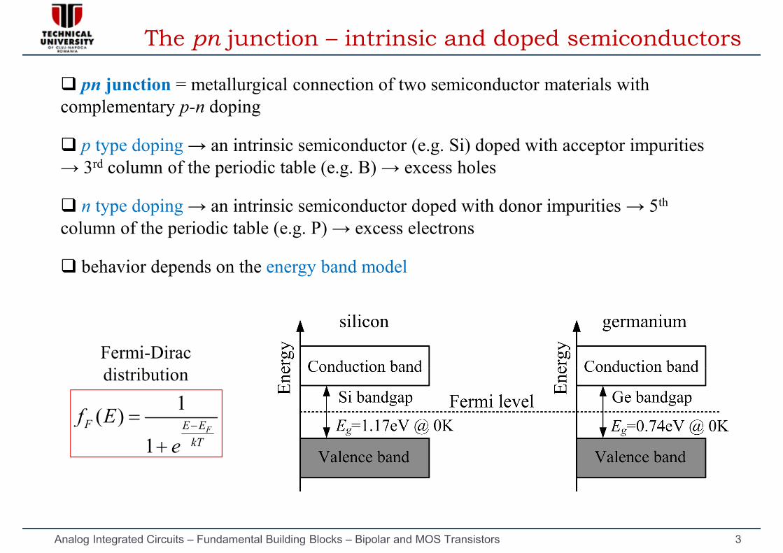
The pn junction – intrinsic and doped semiconductors
pn junction = metallurgical connection of two semiconductor materials with complementary p-n doping
p type doping → an intrinsic semiconductor (e.g. Si) doped with acceptor impurities → 3rd column of the periodic table (e.g. B) → excess holes
n type doping → an intrinsic semiconductor doped with donor impurities → 5th
column of the periodic table (e.g. P) → excess electrons
behavior depends on the energy band model
Fermi-Dirac distribution
Analog Integrated Circuits – Fundamental Building Blocks – Bipolar and MOS Transistors 3
1( )1
FF E EkT
f Ee
distribution

The pn junction – intrinsic and doped semiconductors
doping alters the energy band model of intrinsic semiconductors
the effective band gap decreases and the moving Fermi level facilitates the formation of free carriers → conduction
Analog Integrated Circuits – Fundamental Building Blocks – Bipolar and MOS Transistors 4
at temperatures >0K electrons can move to the conduction band or holes to the valence band → mobile charge carriers → current conduction

The unbiased pn junction – energy band model
unbiased pn junction in equilibrium → intrinsic potential: 0 2ln A DT
i
N NVn
negative and positive ions → internal electric field that accelerates free carriers across the junction boundary → carrier drift and diffusion
Analog Integrated Circuits – Fundamental Building Blocks – Bipolar and MOS Transistors 5
the junction boundary → carrier drift and diffusion
electron-hole recombinations until charge neutrality is achieved and the initial electric field is compensated
depletion region around the junction boundary with ions but no free carriers → effective isolation between p and n type semiconductors

Biasing the pn junction
reverse biasing → biasing enhances the intrinsic field, the depletion region widens and the potential barrier is increased → no conduction
forward biasing → biasing compensates the intrinsic field, the depletion region and the potential barrier decreases → diffusion and sustained current
Analog Integrated Circuits – Fundamental Building Blocks – Bipolar and MOS Transistors 6

The pn junction capacitance and current
doped semiconductors and the isolating depletion region → capacitance
Cj0 depends on donor and acceptor impurity concentrations and on material constants
unbiased junction 0
0
1
jj
D
CC
V
unbiased junction capacitance
external bias voltage
intrinsic potential
the current flowing through the junction → derived from the diffusion equation
Analog Integrated Circuits – Fundamental Building Blocks – Bipolar and MOS Transistors 7
1D
T
VnV
D SI I e
the current flowing through the junction → derived from the diffusion equation
IS – temperature dependent saturation current
VT – thermal voltage
n – junction grading coefficient (=1 for an abrupt junction)

Bipolar junction transistors
bipolar transistor = back to back connection of two pn junctions
current controlled 3-terminal devices:
emitter (E) – source of the carriers
base (B) – controls carrier flow and implicitly the current
collector (C) – captures carriers and eliminates them from the device
npn or pnp depending on the semiconductor types
only npn case discussed, pnp is similar but all biasing and currents are negative
the substrate is sometimes explicitly available → voltage controlled by the designer
Analog Integrated Circuits – Fundamental Building Blocks – Bipolar and MOS Transistors 8

Bipolar junction transistors
unbiased npn transistor in equilibrium → junctions and their energy band model
BEE BCE
the Fermi level is identical for all three layers
both junctions charge neutral with their intrinsic potential and electric field
Analog Integrated Circuits – Fundamental Building Blocks – Bipolar and MOS Transistors 9
both junctions charge neutral with their intrinsic potential and electric field
depleted regions at both junction boundaries
potential barriers → no conduction
device needs biasing → appropriate voltages applied to terminals
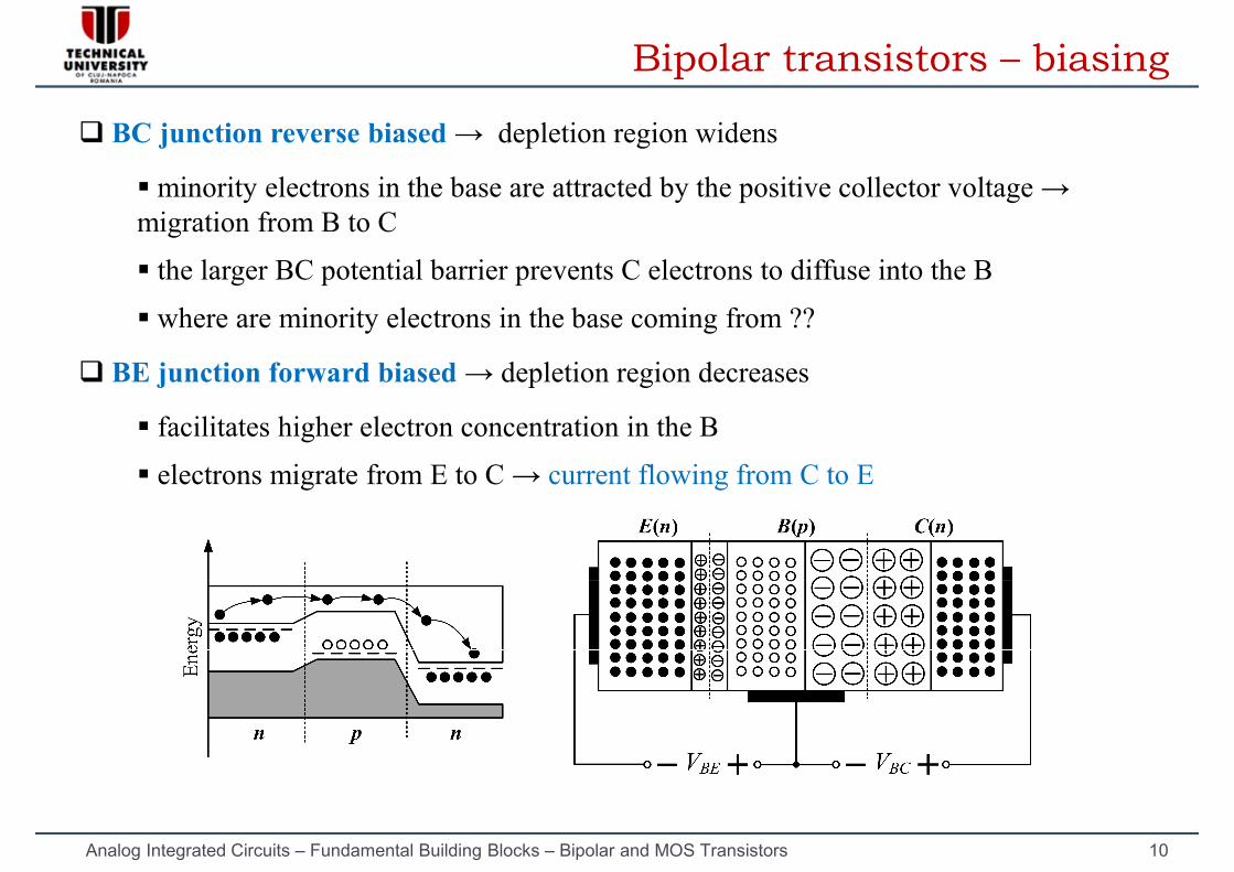
Bipolar transistors – biasing
BC junction reverse biased → depletion region widens
minority electrons in the base are attracted by the positive collector voltage → migration from B to C
the larger BC potential barrier prevents C electrons to diffuse into the B
where are minority electrons in the base coming from ??
BE junction forward biased → depletion region decreases
facilitates higher electron concentration in the B
electrons migrate from E to C → current flowing from C to E
Analog Integrated Circuits – Fundamental Building Blocks – Bipolar and MOS Transistors 10
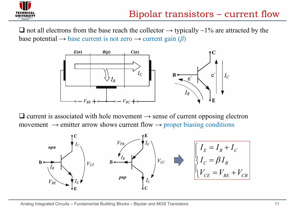
Bipolar transistors – current flow
not all electrons from the base reach the collector → typically ~1% are attracted by the base potential → base current is not zero → current gain (β)
current is associated with hole movement → sense of current opposing electron movement → emitter arrow shows current flow → proper biasing conditions
Analog Integrated Circuits – Fundamental Building Blocks – Bipolar and MOS Transistors 11
E B C
C B
CE BE CB
I I II IV V V

Bipolar transistors simplified fabrication
successive masking, patterning, etching, ion implantation and epitaxial growth
example: vertical npn transistor
Step 1: n+ buried collector implant on a lightly doped p¯ substrate
Step 2: n¯ layer epitaxial growth for vertical collector contact on a lightly doped p¯ substrate vertical collector contact
CC
Analog Integrated Circuits – Fundamental Building Blocks – Bipolar and MOS Transistors 12
CC

Bipolar transistors simplified fabrication
Step 3: implant p+ regions → base diffusion and trench isolation ring
B
B
C
Analog Integrated Circuits – Fundamental Building Blocks – Bipolar and MOS Transistors 13
Alternative trench isolation → etch into the epitaxial layer and create insulator filling
C

Bipolar transistors simplified fabrication
Step 4: implant n+ regions → emitter and deep vertical collector plug
BB
B
C
E
E
Analog Integrated Circuits – Fundamental Building Blocks – Bipolar and MOS Transistors 14
B
C
Junctions are created in a vertical geometry → vertical npn transistor

Bipolar transistors simplified fabrication
Step 5: metal contacts and SiO2 passivation → final transistor
Analog Integrated Circuits – Fundamental Building Blocks – Bipolar and MOS Transistors 15

Bipolar transistors – large signal model
definition of the collector current as a function of biasing voltages, concentration gradients and material constants
Minority electrons diffusing from E to B: 0(0)BE
T
VV
p pn n e
Analog Integrated Circuits – Fundamental Building Blocks – Bipolar and MOS Transistors 16
Recombination gradient in the B: ( ) (0) 1p pB
xn x nW
( ) (0)p p
B
dn x ndx W
0BE
T
S
VE n p V
C E nB
I
qA D nI A J e
W
Collector current: BE
T
VV
C SI I e
saturation current

Bipolar transistors – the Early effect
the collector potential modulates the width of the BC depletion region → the effective width of the base changes
0 0BE BE
T T
V VE n p E n pV VC CB BqA D n qA D nI IW We e
1
EAV
Analog Integrated Circuits – Fundamental Building Blocks – Bipolar and MOS Transistors 17
0 02( ) ( )
T T
S
E n p E n pV VC CB B
CE CE B CE B CE CE B CE
I
I IW We eV V W V W V V W V
EAVVEA - Early voltage
C CEC CE C
CE EA
I VI V IV V
* 1 CEC C C C
EA
VI I I IV
* 1BE
T
VV CE
C SEA
VI I eV
current correction term

Bipolar transistors – saturation
VCE=VBE+VCB → if VCE<VBE → VCB<0 → the BC junction is forward biased
the width of the BC depletion region decreases → current flow
both the BE and BC junctions inject carriers into the base
due to the large carrier concentration in the base the current gain β is not relevant anymore → base current increases significantly
in practice VCE cannot be too small → biasing ! CB
II
Analog Integrated Circuits – Fundamental Building Blocks – Bipolar and MOS Transistors 18

Bipolar transistors – characteristics
non-linear dependence of the collector current IC on VBE and VCE :
transfer characteristic → relevant only in the FAR
output characteristic1
BE
T
VV CE
C SEA
VI I eV
a family of curves also depending on VBE
reflects the operating regions (saturation and FAR)
CE
C BE V ctI f V
Transfer characteristicOutput characteristics
BE
C CE V ctI f V
Analog Integrated Circuits – Fundamental Building Blocks – Bipolar and MOS Transistors 19
OPOP

Small signal model
small signal = infinitely small voltage and current variations
non-linear collector current linearized around the operating point
VCCSImportant: small signal parameters are OP
1 11
BEBE
B CB m
BE BE
Vr I II gV V
11BEV
VC CE CI V Ig I e
small signal base-emitter resistance, hundreds of kΩ
small signal transconductance, mS → slope of the transfer characteristic around
Important: small signal parameters are OP dependent !!!
Analog Integrated Circuits – Fundamental Building Blocks – Bipolar and MOS Transistors 20
1 1BE
T
CE EACE V
CC CVS
CE EA
V Vr II II eV V
11TVC CE Cm S
CE EA T T
I V Ig I eV V V V
slope of the transfer characteristic around the operating point
small signal collector-emitter resistance, hundreds of kΩ → reciprocal of the output characteristic slope around the operating point in the FAR
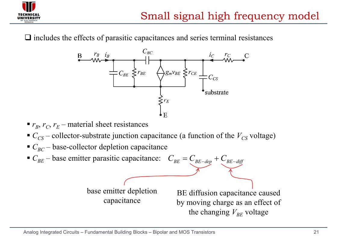
Small signal high frequency model
includes the effects of parasitic capacitances and series terminal resistances
rB, rC, rE – material sheet resistances CCS – collector-substrate junction capacitance (a function of the VCS voltage) CBC – base-collector depletion capacitance CBE – base emitter parasitic capacitance: C C C
Analog Integrated Circuits – Fundamental Building Blocks – Bipolar and MOS Transistors 21
CBE – base emitter parasitic capacitance: BE BE dep BE diffC C C
base emitter depletion capacitance
BE diffusion capacitance caused by moving charge as an effect of
the changing VBE voltage

Small signal high frequency model
capacitances → β is frequency dependent → β(s)
determine the frequency response1 1|| ||
C m BE
BE B BEBE BC
i g v
v i rsC sC
collector grounded, emitter and collector sheet resistances neglected
BE BCsC sC
0( )
1 BE BE BC
ss r C C
Analog Integrated Circuits – Fundamental Building Blocks – Bipolar and MOS Transistors 22
fT – transit frequency

Enhancement mode MOS transistors
enhancement mode MOS (Metal-Oxide-Semiconductor) transistors = voltage controlled 4-terminal devices:
sources (S) – source of the majority carriers
gate (G) – electrically isolated control terminal gate (G) – electrically isolated control terminal
drain (D) – carrier target terminal when moving through the device
substrate or bulk (B) – contact in most case explicitly available and needs biasing
n-channel (NMOS) or p-channel (PMOS) depending on the semiconductor types
only NMOS case discussed, PMOS is similar but all biasing and currents are negative
Analog Integrated Circuits – Fundamental Building Blocks – Bipolar and MOS Transistors 23
analog digital

MOS transistors – structure
typical n-well fabrication process with a lightly doped p¯ substrate
NMOS transistors are created on the substrate, while PMOS sits in a n-well
Analog Integrated Circuits – Fundamental Building Blocks – Bipolar and MOS Transistors 24
NMOS transistors are created on the substrate, while PMOS sits in a n-well
polysilicon gate isolated from the semiconductor by a thin SiO2 isolation layer
substrate (bulk) contacts available for biasing (see latch-up later)
devices are isolated from each other by trench isolations (similar with BJT)
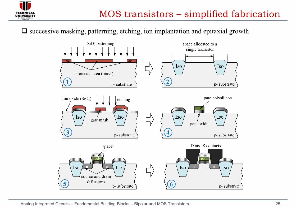
MOS transistors – simplified fabrication
successive masking, patterning, etching, ion implantation and epitaxial growth
1 2
3 4
Analog Integrated Circuits – Fundamental Building Blocks – Bipolar and MOS Transistors 25
5 6
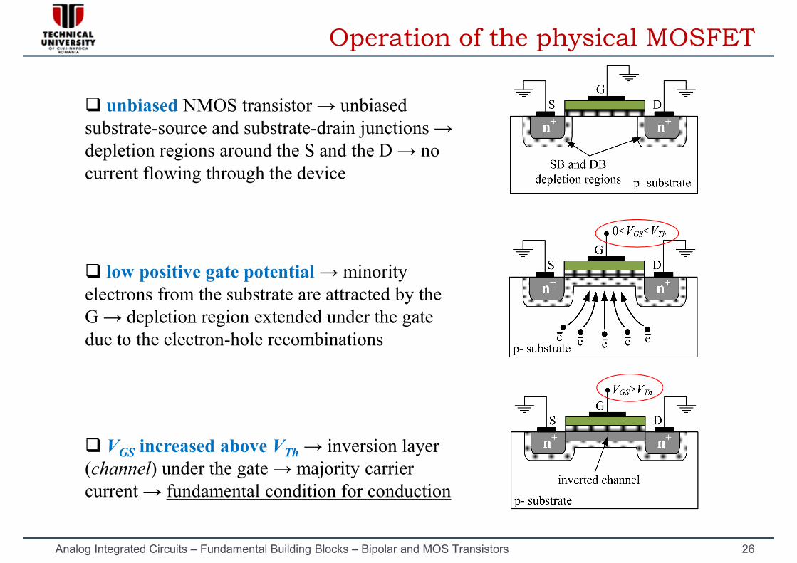
Operation of the physical MOSFET
unbiased NMOS transistor → unbiased substrate-source and substrate-drain junctions → depletion regions around the S and the D → no current flowing through the device
low positive gate potential → minority electrons from the substrate are attracted by the G → depletion region extended under the gate due to the electron-hole recombinations
Analog Integrated Circuits – Fundamental Building Blocks – Bipolar and MOS Transistors 26
VGS increased above VTh → inversion layer (channel) under the gate → majority carrier current → fundamental condition for conduction

Operation of the physical MOSFET
low VDS voltage → substrate-drain junction reverse biased → the depletion region is extended around the D → channel asymmetry
carriers are accelerated toward the D through the S-D ohmic contact → triode (linear) regionthe S-D ohmic contact → triode (linear) region→ voltage controlled resistor
VDS ≥ VDSat → the drain side depletion region causes a channel pinch-off → saturation
Operating
Analog Integrated Circuits – Fundamental Building Blocks – Bipolar and MOS Transistors 27
Operating region VGS VDS Channel
cut-off < VThdoes not matter
unless breakdown no
triode (linear) > VTh 0 < VDS < VDsat yes, no pinch-off
saturation > VTh VDS > VDsat yes, pinch-off

The large signal model
large signal model → dependence of the drain current ID on VGS and VDS
2
ox DSC W VI V V V
Triode region
2
ox DSD GS Th DS
DS DSat
C W VI V V VL
V V
2
2ox
D GS Theff
DS DSat
C WI V VL
V V
Saturation DSat GS ThV V V
Channel length modulation:
( )eff pinch DSL L X V
pinch pinchD D DX XI I I
Analog Integrated Circuits – Fundamental Building Blocks – Bipolar and MOS Transistors 28
µ – carrier mobility Cox – specific oxide capacitance (εox/tox)W, L – transistor width and length Leff – effective channel length λ – channel length modulation parameter
pinch pinchD D DD
DS pinch DS eff DS
X XI I I IV X V L V
2* 12
oxDD D DS GS Th DS
DS
C WII I V V V VV L
correction term

Substrate biasing
parasitic bipolar transistors and sheet resistances in adjacent NMOS and PMOS devices create a positive feedback loop → equivalent silicon controlled rectifier (SCR) or thyristor
any disturbance may trigger the loop and create a virtual short circuit between supply rails → latch-up
each bipolar transistor base must be deactivated → substrate grounded for NMOS ( p type base) and connected to positive supply for PMOS (n type base)
Analog Integrated Circuits – Fundamental Building Blocks – Bipolar and MOS Transistors 29
0 0 02 | | 2 | |Th BS Th BSV V V V The effect of VBS on the threshold voltage:

The small signal model in saturation
infinitely small voltage and current variations → non-linear drain current linearized around the operating point
Important: small signal parameters
mD gIg
2 2D D Dm
GS DSat ox
I I LIgV V C W
substrate transconductance, a fraction of gm
small signal transconductance, hundreds of µS → slope of the ID(VGS) characteristic around the operating point
Important: small signal parameters are OP dependent !!!
Analog Integrated Circuits – Fundamental Building Blocks – Bipolar and MOS Transistors 30
02 | | | 2 |mD
mbBS BS
gV V
1 1DSDS
D DDsat
DS sat
VrI II
V
substrate transconductance, a fraction of gm(~ 20-25% for short channel MOSFET)
small signal drain-source resistance, hundreds of kΩ → reciprocal of the ID(VDS) characteristic slope around the operating point in the saturation region

Parasitic capacitances in MOS transistors
0BSjBS
CC 0BDjBD
CC
OLS OLD OL oxC C WL C
COLS, COLD – source and drain overlap capacitances
CjBS,CjBD, CjBch – source-substrate, drain-substrate and channel substrate junction capacitances
0
1jBS
BS
BS
CV
0
1jBD
BD
BD
CV
Analog Integrated Circuits – Fundamental Building Blocks – Bipolar and MOS Transistors 31
capacitances
Cch – gate-channel (or simply channel) capacitance → operating region dependent
Each capacitance contributes to the overall terminal-to-terminal parasitic capacitance depending on the operating region.
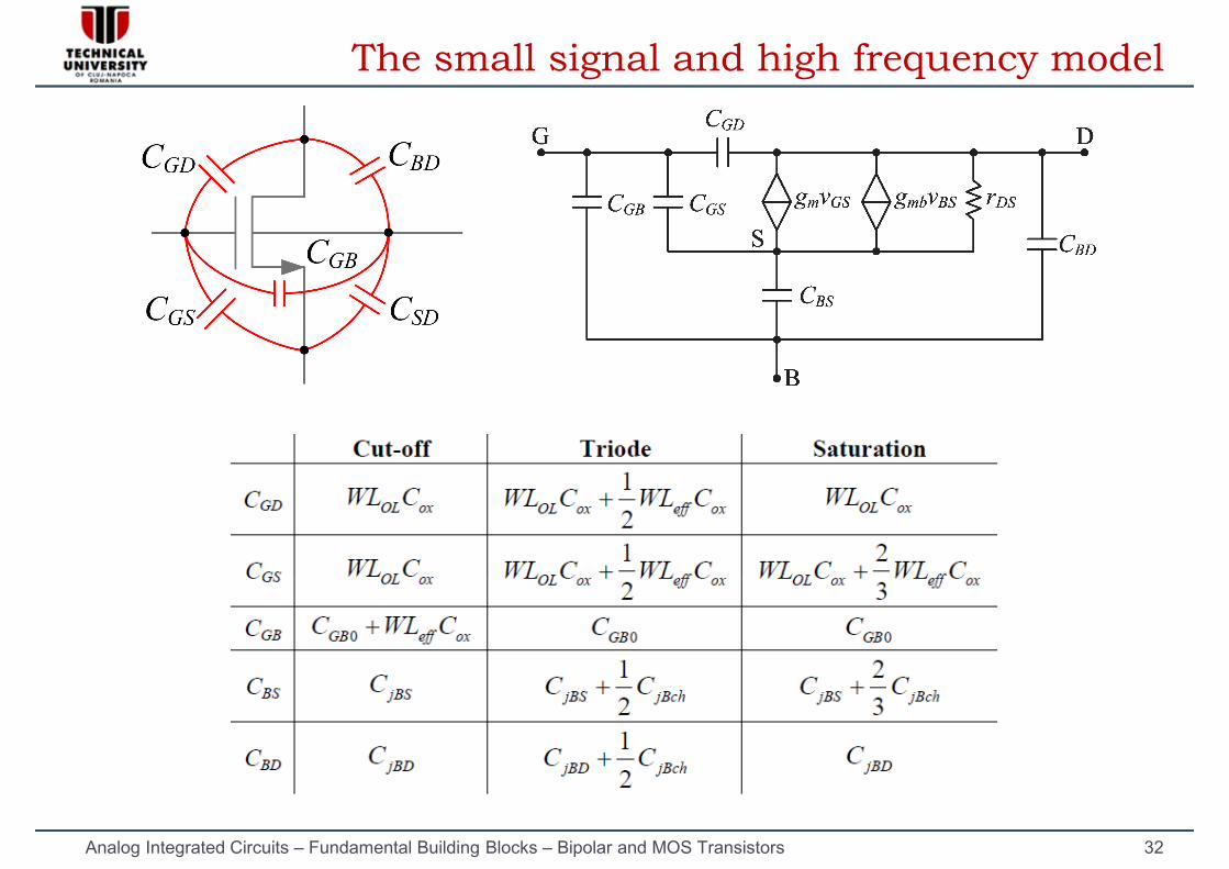
The small signal and high frequency model
Analog Integrated Circuits – Fundamental Building Blocks – Bipolar and MOS Transistors 32

Bibliography
B. van Zeghebroeck, Principles of Semiconductor Devices, online book, http://ecee.colorado.edu/~bart/book/book/index.html
P.E. Allen, D.R. Holberg, CMOS Analog Circuit Design, Oxford University Press, 2002 P.E. Allen, D.R. Holberg, CMOS Analog Circuit Design, Oxford University Press, 2002
B. Razavi, Design of Analog CMOS Integrated Circuits, McGraw-Hill, 2002
D. Johns, K. Martin, Analog Integrated Circuit Design, Wiley, 1996
Analog Integrated Circuits – Fundamental Building Blocks – Bipolar and MOS Transistors 33