Semiconductors and PN junction diode
53
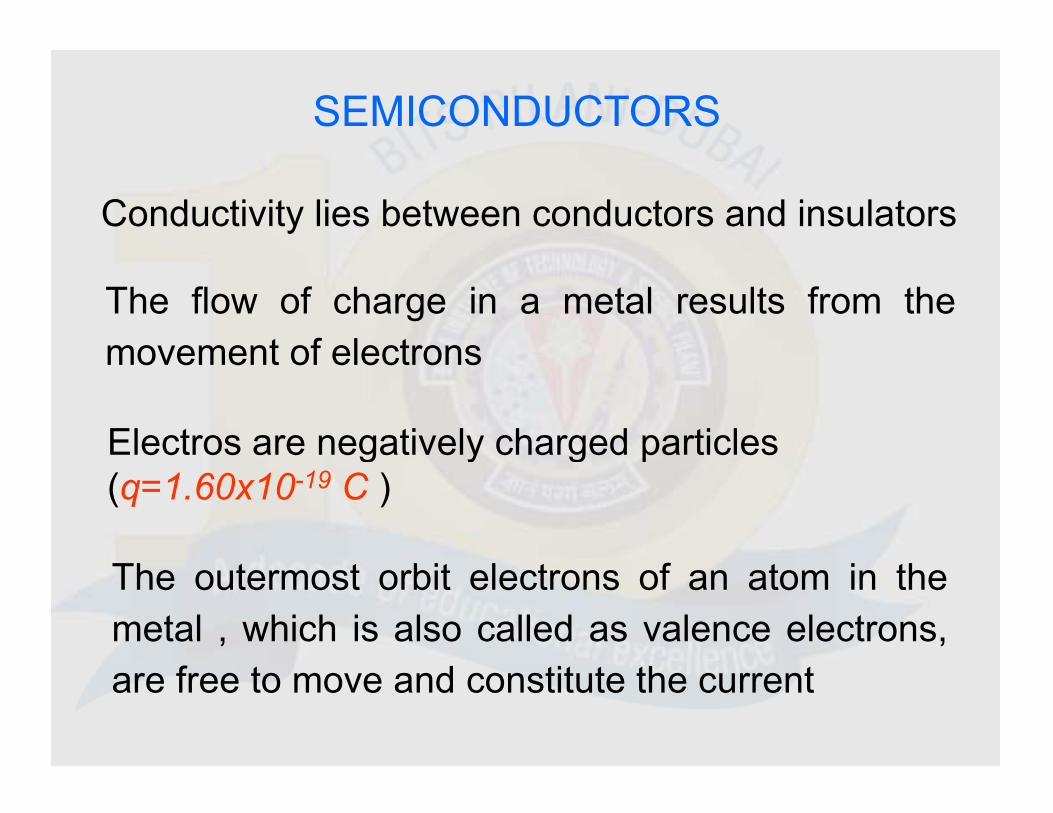
SEMICONDUCTORS Conductivity lies between conductors and insulators The flow of charge in a metal results from the movement of electrons movement of electrons Electros are negatively charged particles (q=1.60x10 -19 C ) The outermost orbit electrons of an atom in the metal , which is also called as valence electrons, are free to move and constitute the current
Transcript of Semiconductors and PN junction diode
SEMICONDUCTORS
Conductivity lies between conductors and insulators
The flow of charge in a metal results from themovement of electronsmovement of electrons
Electros are negatively charged particlesg y g p(q=1.60x10⁻¹⁹ C )
The outermost orbit electrons of an atom in themetal , which is also called as valence electrons,are free to move and constitute the current
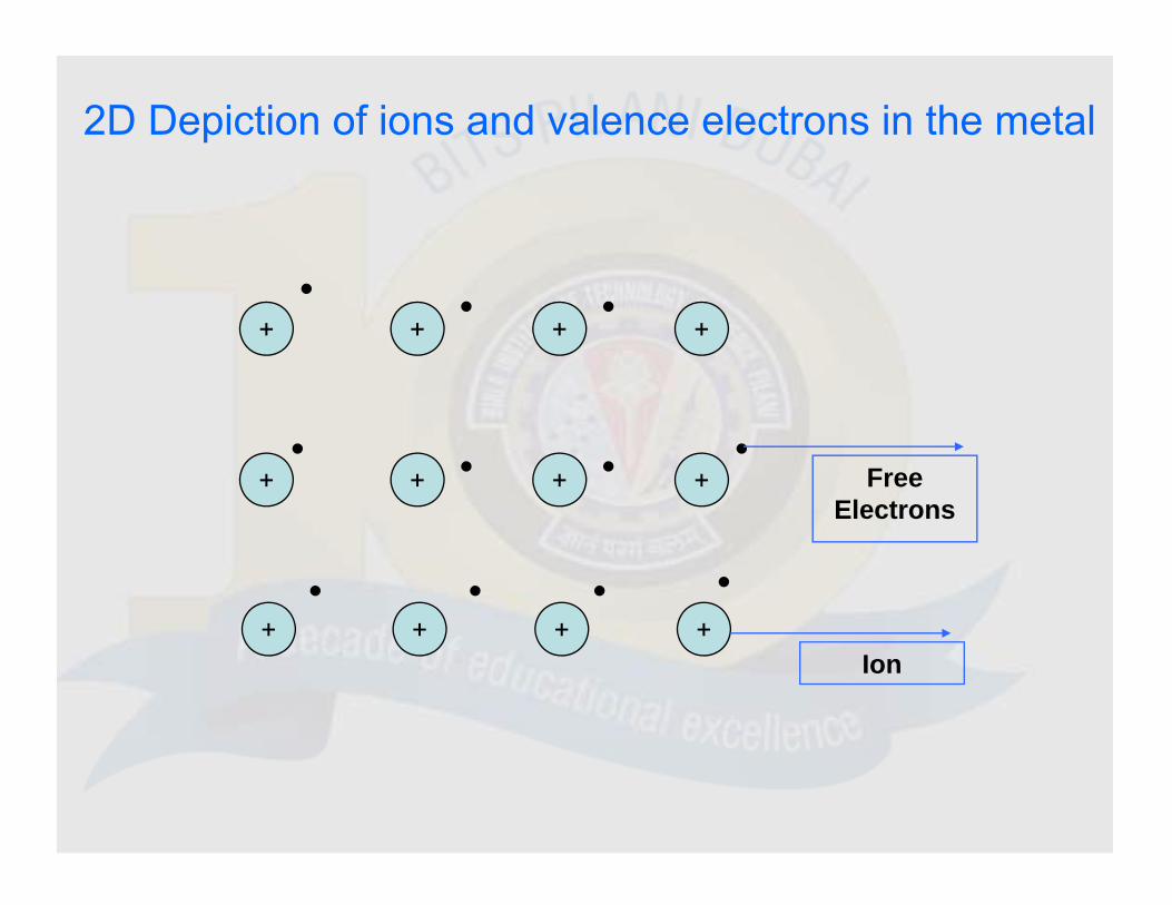
2D Depiction of ions and valence electrons in the metal
+ + + +
+ + + + Free Electrons
+ + + +
Electrons
+ + + +Ion

Due to the thermal energy the free electrons are incontinuous motion
These electrons will collide with the ions and directionf th ti hof the motion changes
If lt i li d t t l th th dIf no voltage is applied to a metal , then the random motion of the electrons results in zero average currentresults in zero average current
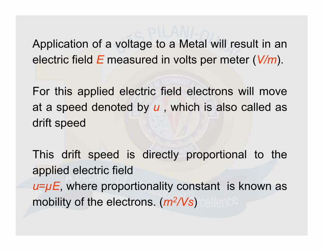
Application of a voltage to a Metal will result in anApplication of a voltage to a Metal will result in anelectric field E measured in volts per meter (V/m).
For this applied electric field electrons will moveat a speed denoted by u which is also called asat a speed denoted by u , which is also called asdrift speed
This drift speed is directly proportional to theapplied electric fieldapplied electric fieldu=µE, where proportionality constant is known asmobility of the electrons (m2/Vs)mobility of the electrons. (m /Vs)

Let us consider a metallic conductor of length Land has a cross section area of A square meterand has a cross section area of A square meter
A N Free electrons
L
Let N be the number of free electrons in thissection of the conductor and moves to the left withthe drift speed of u.If an electron takes T seconds to travel L meters ,then drift speed u=L/T, we can write T=L/u.

Flow of N electrons to left in T seconds means acurrent i going to the rightcurrent i going to the rightWhere
LNqu
uLNq
TNqi
/ LuLT /
The current density iJ A
J
Th hNquJThus we have ALqJ
LA is the volume of the conductor section andLA is the volume of the conductor section andnumber of free electrons is N , density of the freeelectron is n=N/LA, which is called as freefree electronelectronelectron is n N/LA, which is called as freefree electronelectronconcentrationconcentration. (m-3)
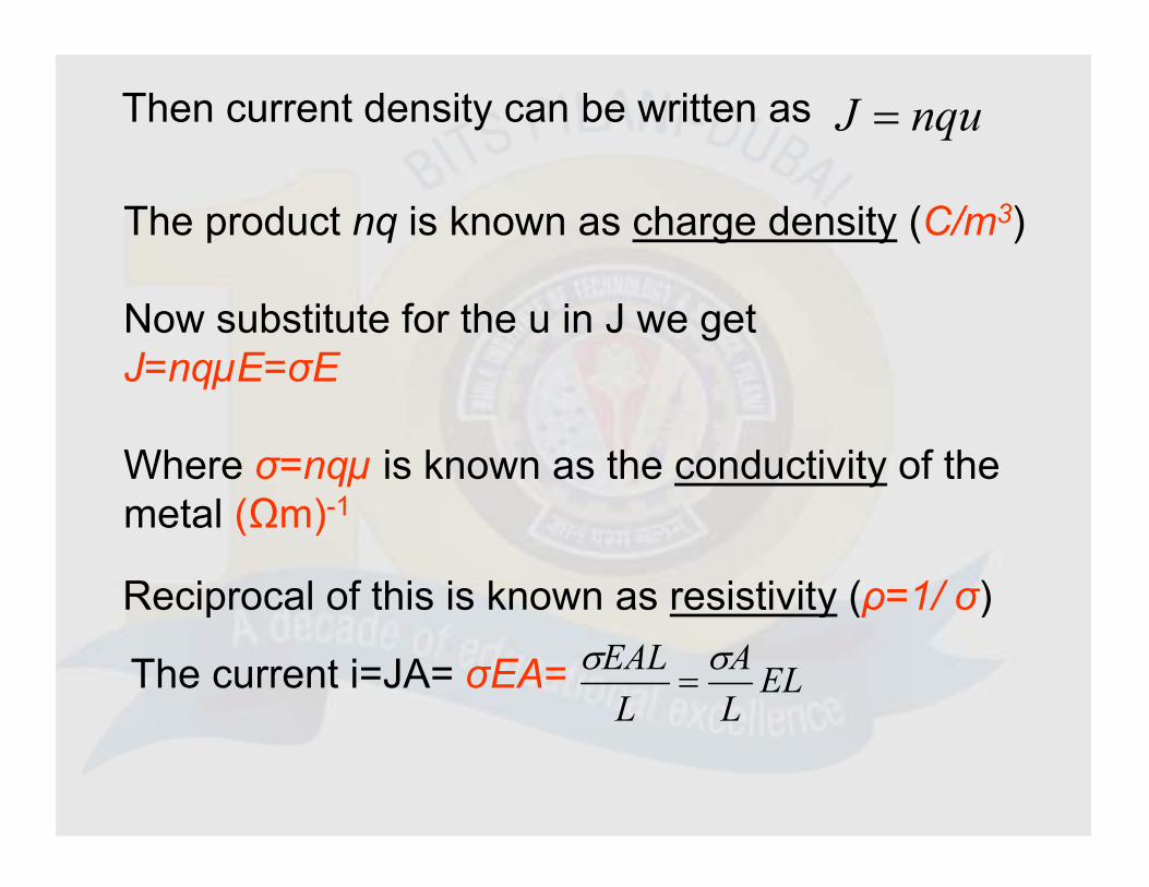
Then current density can be written as nquJ
The product nq is known as charge density (C/m3)
Now substitute for the u in J we getJ=nqµE=σEqµ
Where σ=nqµ is known as the conductivity of the t l (Ω ) 1metal (Ωm)-1
Reciprocal of this is known as resistivity (ρ=1/ σ)p y (ρ )
The current i=JA= σEA= ELLA
LEAL
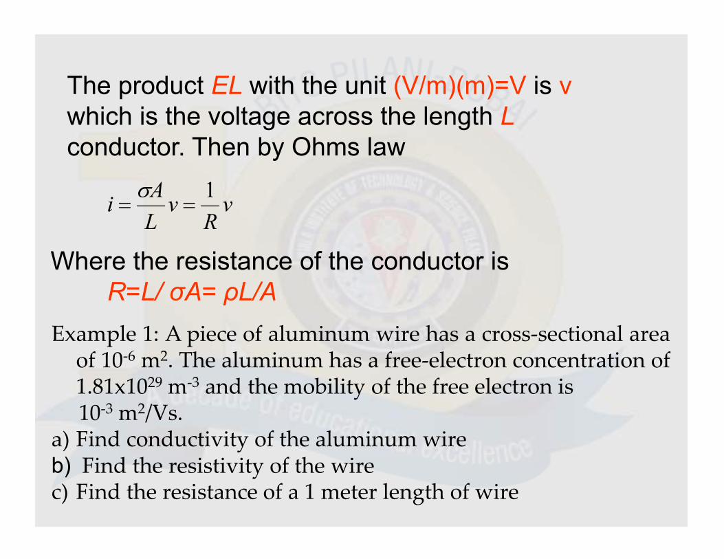
The product EL with the unit (V/m)(m)=V is v which is the voltage across the length Lconductor. Then by Ohms law
vR
vLAi 1
Where the resistance of the conductor is R=L/ σA= ρL/A
Example 1: A piece of aluminum wire has a cross‐sectional areaof 10‐6 m2. The aluminum has a free‐electron concentration of1 81x1029 m‐3 and the mobility of the free electron is1.81x1029 m 3 and the mobility of the free electron is10‐3 m2/Vs.
a) Find conductivity of the aluminum wireb) Find the resistivity of the wirec) Find the resistance of a 1 meter length of wire

Solution:Given: A= 10-6 m2 , n= 1.81x1029 m-3 and µ= 10-3 m2/Vs, µ
a) conductivity of the aluminum wire (σ=nqµ )) y ( qµ )
σ= (1.81x1029)(1.6x10⁻¹⁹)(10-3)= 2.9x10⁷ mho/m
b) Find the resistivity of the wire (ρ=1/ σ)b) Find the resistivity of the wire (ρ=1/ σ)ρ=1/2.9x107=3.345x10-8 Ωm
c) resistance of a 1 meter length of wire R= ρL/AR=(3.345x10-8)(1)/10-6 = 34.5 mΩ

Intrinsic (Pure) Semiconductor)
• Semiconductors such as Si and Ge have 4electrons (tetravalent) in the outermost shell
• In crystal structure of these materials, atoms arearranged in tetrahedron structure with one atomat each vertex
• Each atom contributes 4 valence electrons to thecrystal; Each atom shares one electron eachfrom its 4 neighbors, thus forming covalent bondg , g
• Because of covalent bonding, electrons aretightly bound to crystal – not available fortightly bound to crystal not available forconduction
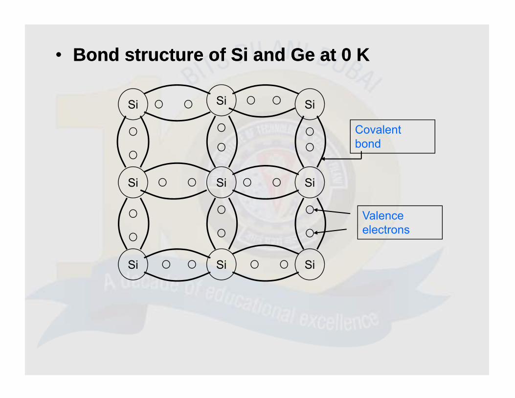
•• Bond structure of Si and Ge at 0 KBond structure of Si and Ge at 0 K
SiSiSi
Covalent bond
Si SiSi
Valence
Si SiSi
electrons

At room temperature, due to thermal energy oneelectron will be detached and makes an vacancy inythat position which is called as hole.
SiSiSi
Covalent
Si SiSi
bond
Valence electrons
Hole
Si SiSi
Free electron
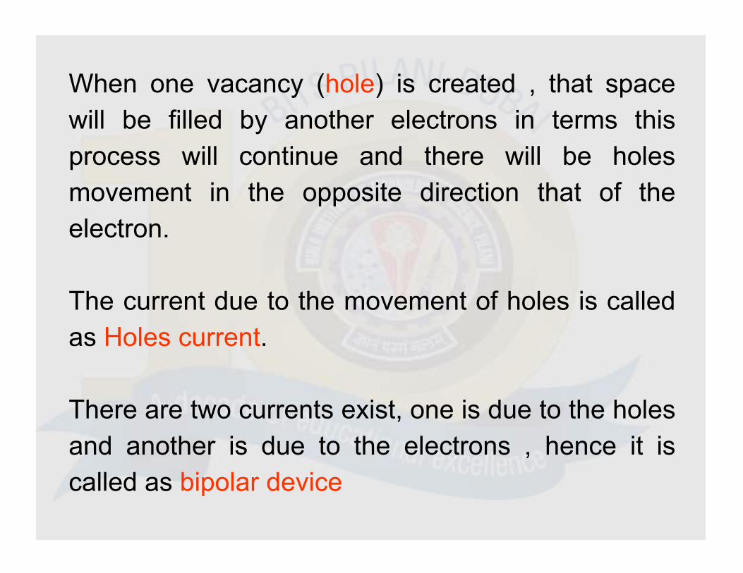
When one vacancy (hole) is created , that spacewill be filled by another electrons in terms thisprocess will continue and there will be holesmovement in the opposite direction that of theelectron.
The current due to the movement of holes is calledas Holes current.
There are two currents exist, one is due to the holesand another is due to the electrons , hence it iscalled as bipolar device
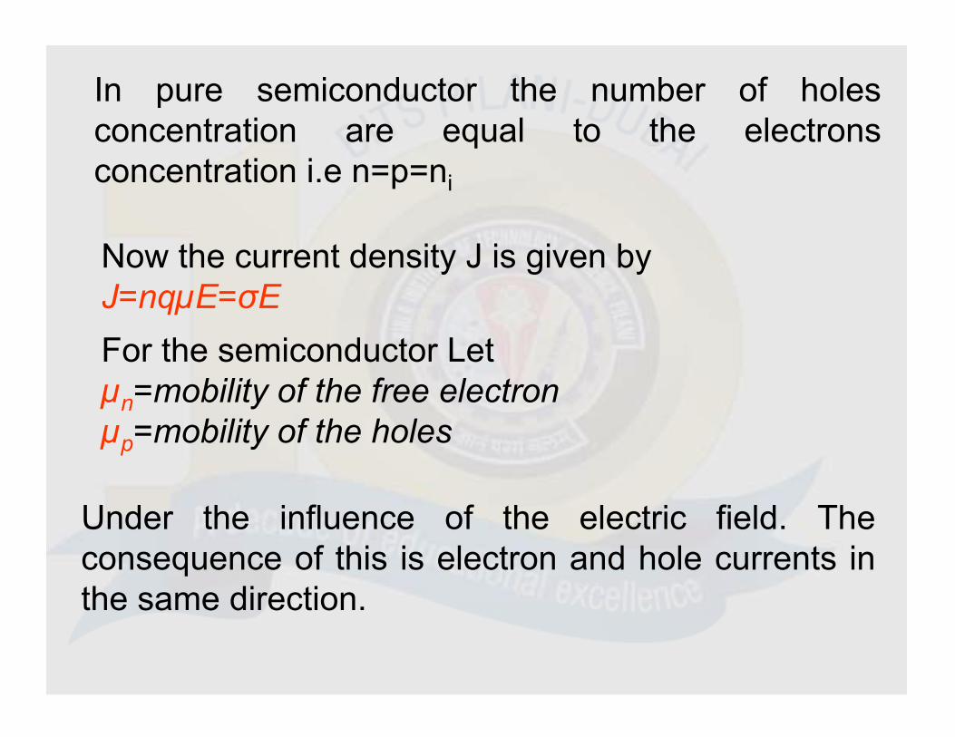
In pure semiconductor the number of holesconcentration are equal to the electronsconcentration are equal to the electronsconcentration i.e n=p=ni
Now the current density J is given by J=nqµE=σEFor the semiconductor Letµn=mobility of the free electronµp=mobility of the holes
U d th i fl f th l t i fi ld ThUnder the influence of the electric field. Theconsequence of this is electron and hole currents inthe same directionthe same direction.

The current density J is given byJ=(nµ +pµ )qE=σEJ=(nµn+pµp)qE=σEσ=(nµn+pµp)q is conductivity of the semiconductor
At 300 K, the intrinsic concentration of germanium(GE) is 2.5x10¹⁹ m-3 Furthermore, the free-electron( ) ,mobility is 0.38 m2/Vs and the hole mobility is 0.18m2/Vs. Find the conductivity and resistivity of the puregermanium.
Given ni=2.5x10¹⁹ , µn= 0.38 µp=0.18
Answers : Conductivity= 2.25 mho/m Resistivity = 0 446 Ω mResistivity = 0.446 Ω m
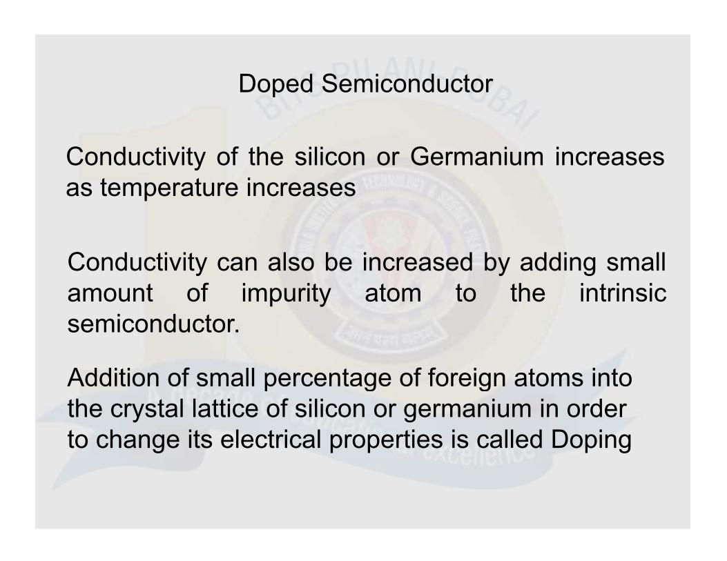
Doped Semiconductor
Conductivity of the silicon or Germanium increasesas temperature increases
Conductivity can also be increased by adding smallamount of impurity atom to the intrinsic
i d tsemiconductor.
Addition of small percentage of foreign atoms into p g gthe crystal lattice of silicon or germanium in order to change its electrical properties is called Doping
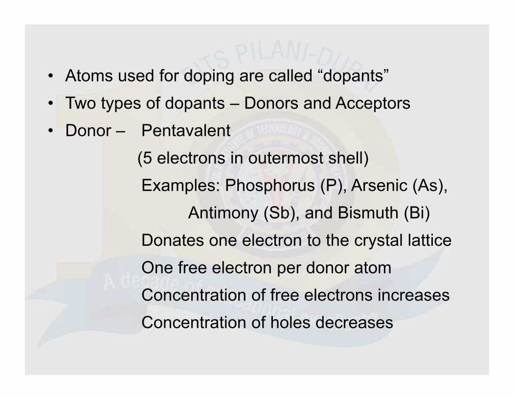
• Atoms used for doping are called “dopants”• Atoms used for doping are called dopants• Two types of dopants – Donors and Acceptors• Donor – Pentavalent
(5 electrons in outermost shell)Examples: Phosphorus (P), Arsenic (As),
Antimony (Sb), and Bismuth (Bi)Donates one electron to the crystal latticeOne free electron per donor atompConcentration of free electrons increasesConcentration of holes decreasesConcentration of holes decreases

N-type semiconductor
SiSiSi
Free electron
P SiSi
Si SiSi
Electrons are majority charge carriersHoles are minority charge carriers
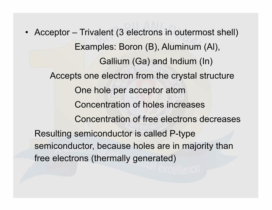
• Acceptor – Trivalent (3 electrons in outermost shell)Examples: Boron (B), Aluminum (Al),
Gallium (Ga) and Indium (In)( ) ( )Accepts one electron from the crystal structure
One hole per acceptor atomOne hole per acceptor atomConcentration of holes increasesConcentration of free electrons decreasesConcentration of free electrons decreases
Resulting semiconductor is called P-type semiconductor because holes are in majority thansemiconductor, because holes are in majority than free electrons (thermally generated)

• P-type semiconductor
SiSiSi
B SiSi
Hole
Si SiSi
Holes are majority charge carriersElecrons are minority charge carriersElecrons are minority charge carriers
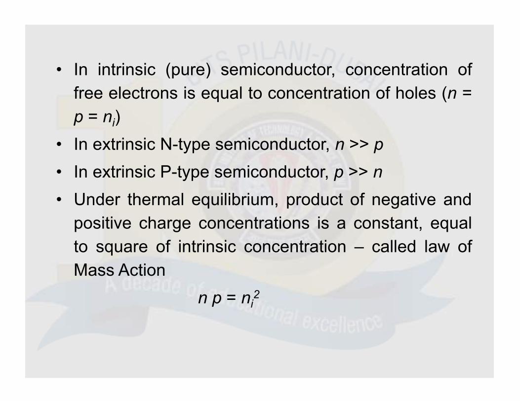
• In intrinsic (pure) semiconductor, concentration ofIn intrinsic (pure) semiconductor, concentration offree electrons is equal to concentration of holes (n =p = ni)p i)
• In extrinsic N-type semiconductor, n >> p• In extrinsic P-type semiconductor p >> nIn extrinsic P type semiconductor, p >> n• Under thermal equilibrium, product of negative and
positive charge concentrations is a constant equalpositive charge concentrations is a constant, equalto square of intrinsic concentration – called law ofMass Action
n p = ni2
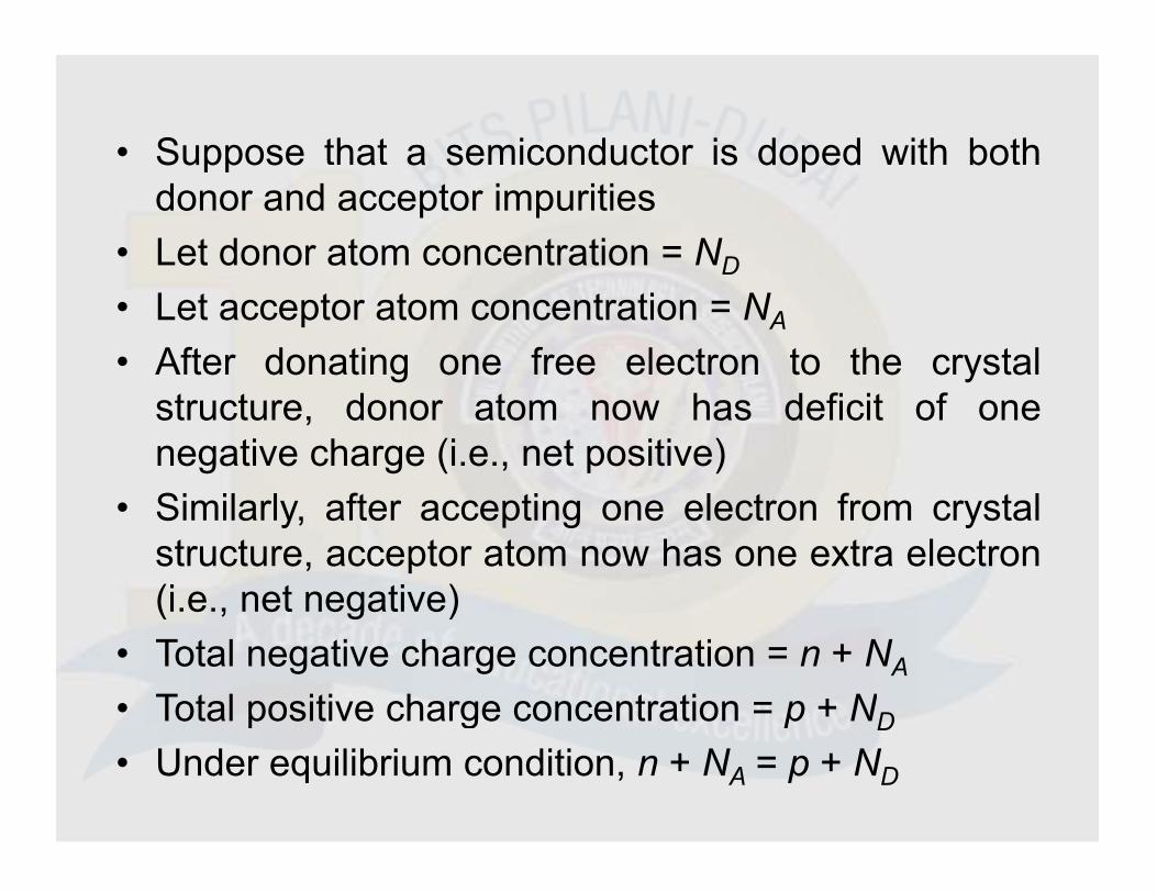
• Suppose that a semiconductor is doped with bothSuppose a a se co duc o s doped bodonor and acceptor impurities
• Let donor atom concentration = ND
• Let acceptor atom concentration = NA
• After donating one free electron to the crystalstructure, donor atom now has deficit of onenegative charge (i.e., net positive)
• Similarly after accepting one electron from crystal• Similarly, after accepting one electron from crystalstructure, acceptor atom now has one extra electron(i.e., net negative)( , g )
• Total negative charge concentration = n + NA
• Total positive charge concentration = p + NDp g p D
• Under equilibrium condition, n + NA = p + ND

• In N-type semiconductor NA = 0 HenceIn N-type semiconductor, NA = 0. Hencen = p + ND
But n >> p Hence n ≈ NDBut n >> p. Hence n ND
Now, p = ni2/n = ni
2 / ND
• Similarly in P-type semiconductor, ND = 0. HenceSimilarly in P type semiconductor, ND 0. Hencep = n + NA
But p >> n. Hence p ≈ NAp p A
Now, n = ni2/p = ni
2 / NA
• Note: If ND = NA then, semiconductor behaves likeD A ,intrinsic
• If ND > NA then semiconductor is N-type• If NA > ND then semiconductor is P-type
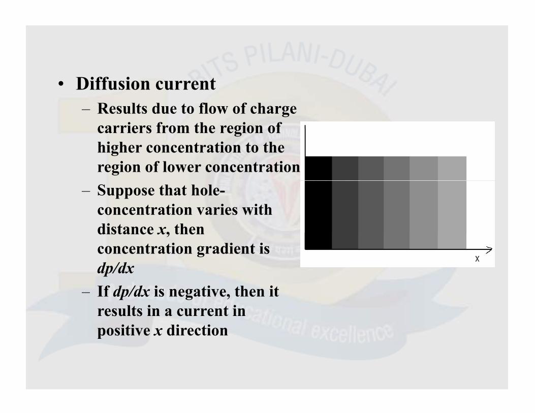
• Diffusion current– Results due to flow of charge
carriers from the region ofcarriers from the region of higher concentration to the region of lower concentration
– Suppose that hole-concentration varies with distance x, thendistance x, then concentration gradient is dp/dx
– If dp/dx is negative, then it results in a current in positive x directionp
PN-Junction
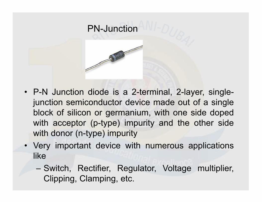
• P-N Junction diode is a 2-terminal, 2-layer, single-junction semiconductor device made out of a singleblock of silicon or germanium with one side dopedblock of silicon or germanium, with one side dopedwith acceptor (p-type) impurity and the other sidewith donor (n-type) impurity
• Very important device with numerous applicationslike– Switch, Rectifier, Regulator, Voltage multiplier,
Clipping, Clamping, etc.
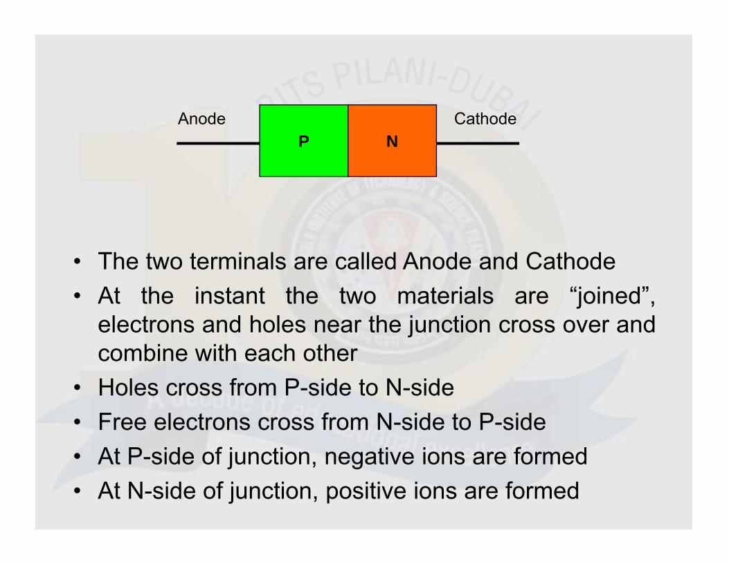
P NAnode Cathode
• The two terminals are called Anode and Cathode• At the instant the two materials are “joined”,
l t d h l th j ti delectrons and holes near the junction cross over andcombine with each other
• Holes cross from P side to N side• Holes cross from P-side to N-side• Free electrons cross from N-side to P-side• At P-side of junction negative ions are formed• At P-side of junction, negative ions are formed• At N-side of junction, positive ions are formed
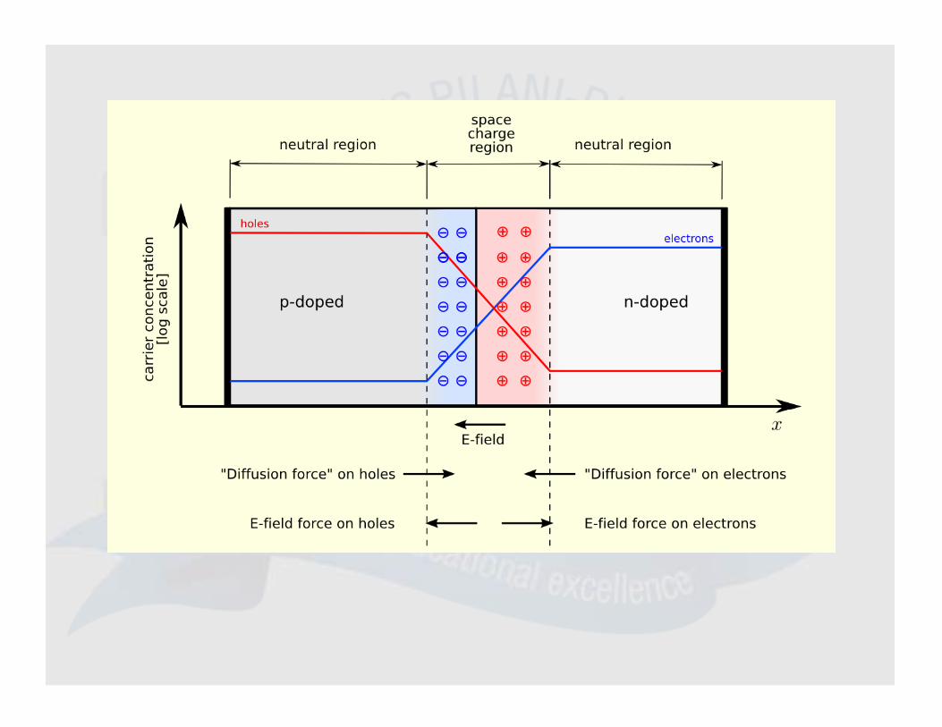
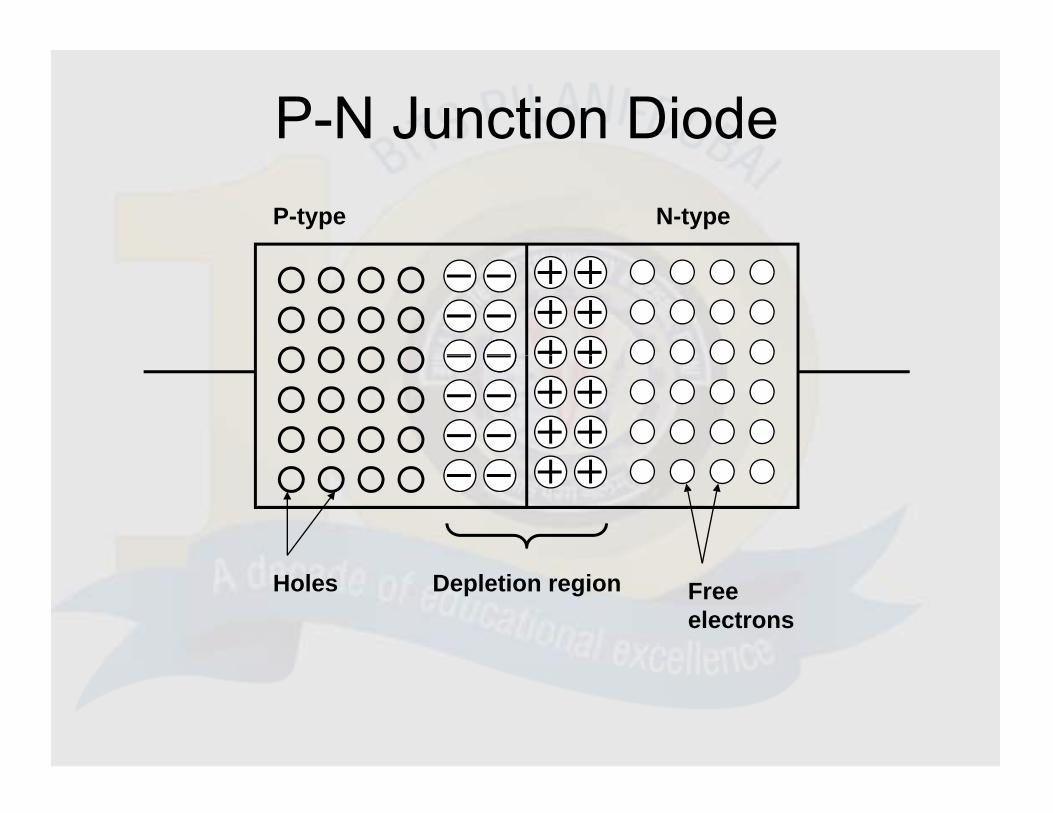
P-N Junction DiodeP-type N-type
Depletion regionHoles Free electrons
• Depletion region is the region having no free carriersDepletion region is the region having no free carriers• Further movement of electrons and holes across the
junction stops due to formation of depletion regionjunction stops due to formation of depletion region• Depletion region acts as barrier opposing further
diffusion of charge carriers So diffusion stopsdiffusion of charge carriers. So diffusion stopswithin no time
• Current through the diode under no-bias condition isCurrent through the diode under no bias condition iszero
• BiasBias– Application of external voltage across the two
terminals of the deviceterminals of the device
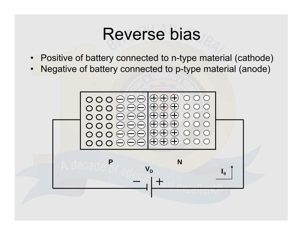
Reverse bias• Positive of battery connected to n-type material (cathode)• Negative of battery connected to p-type material (anode)g y p yp ( )
P NVD
P NI0
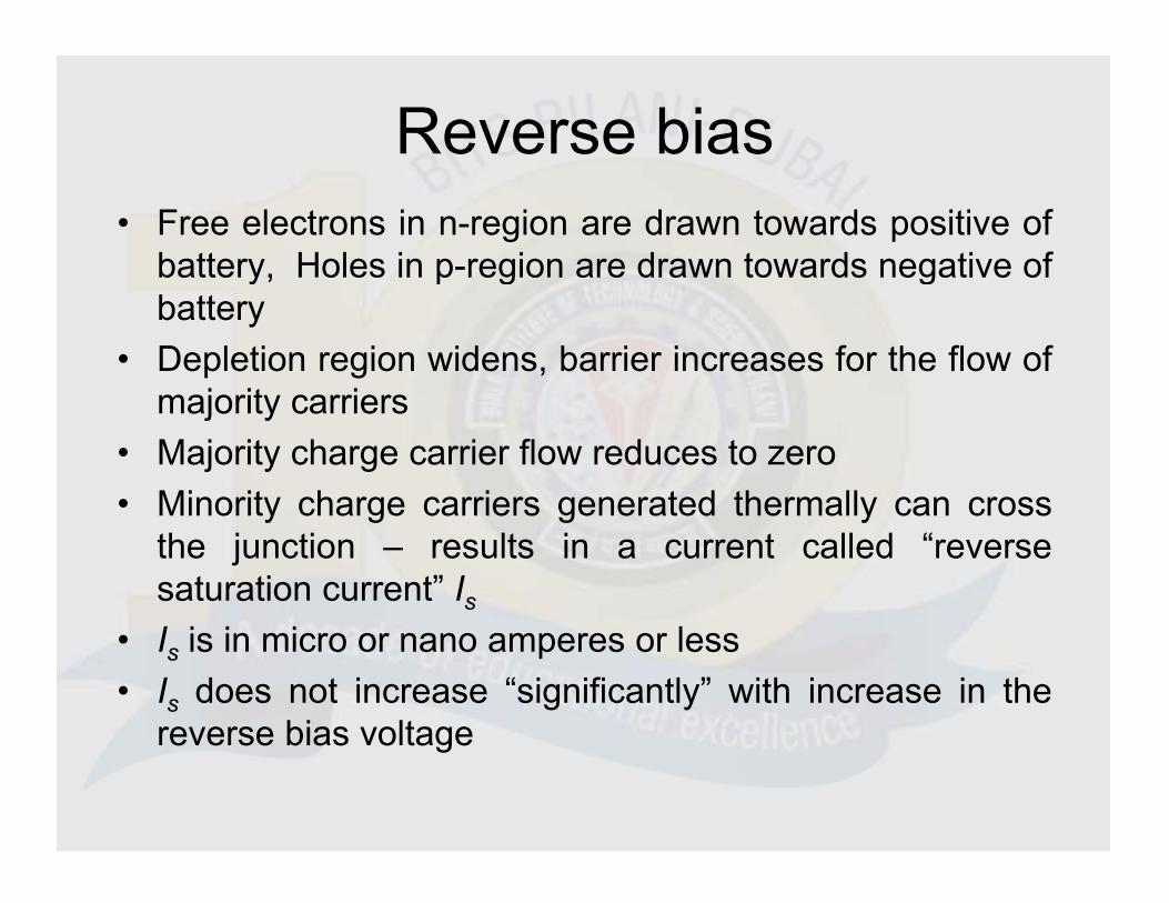
Reverse bias• Free electrons in n-region are drawn towards positive of
battery, Holes in p-region are drawn towards negative ofy, p g gbattery
• Depletion region widens, barrier increases for the flow ofmajorit carriersmajority carriers
• Majority charge carrier flow reduces to zero• Minority charge carriers generated thermally can crossMinority charge carriers generated thermally can cross
the junction – results in a current called “reversesaturation current” Is
• Is is in micro or nano amperes or less• Is does not increase “significantly” with increase in the
reverse bias voltagereverse bias voltage
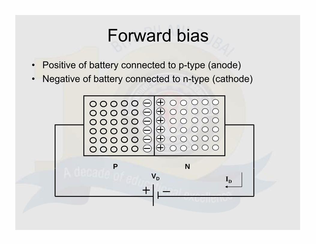
Forward bias• Positive of battery connected to p-type (anode)
N ti f b tt t d t t ( th d )• Negative of battery connected to n-type (cathode)
P NVD
P NID

Forward bias• Electrons in n-type are forced to recombine with
positive ions near the boundary, similarly holes in p-p y y ptype are forced to recombine with negative ions
• Depletion region width reducesp g• An electron in n-region “sees” a reduced barrier at
the junction and strong attraction for positivej g ppotential
• As forward bias is increased, depletion region, p gnarrows down and finally disappears – leads toexponential rise in current
• Forward current is measured in milli amperes
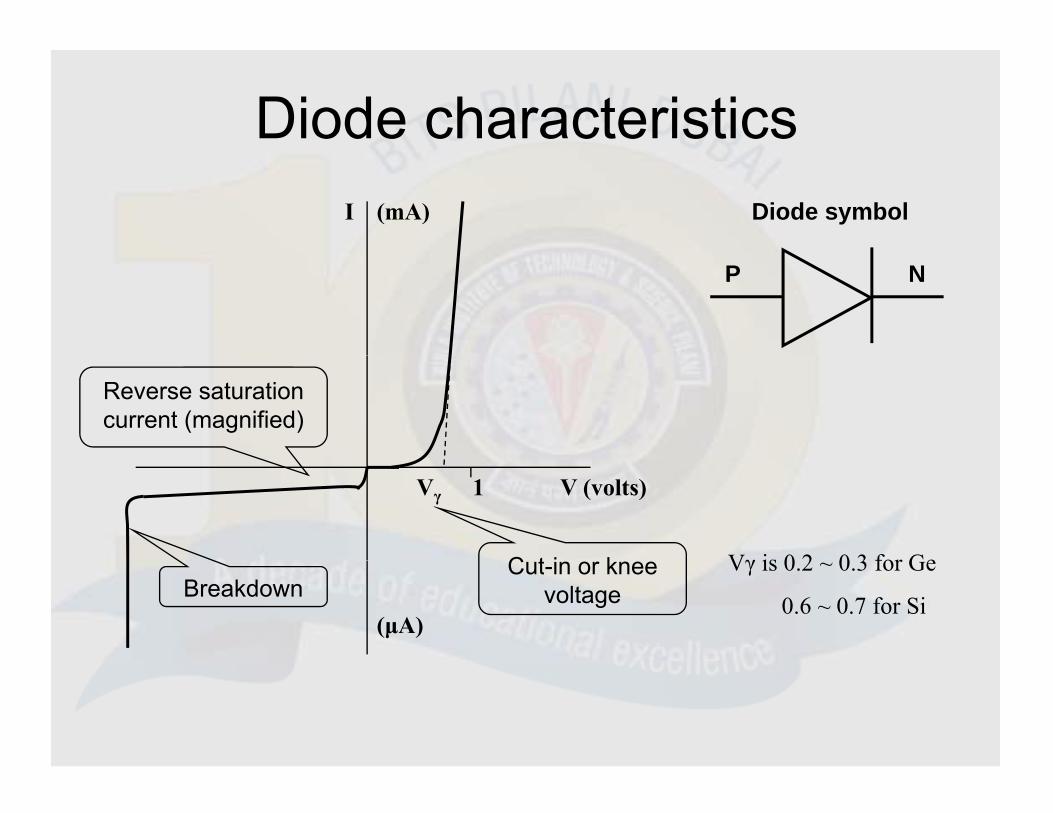
Diode characteristicsDiode symbol(mA)I
P N
Reverse saturation current (magnified)
Vγ is 0 2 0 3 for Ge
V (volts)Vγ 1
C t i k Vγ is 0.2 ~ 0.3 for Ge
0.6 ~ 0.7 for Si(μA)
Cut-in or knee voltageBreakdown
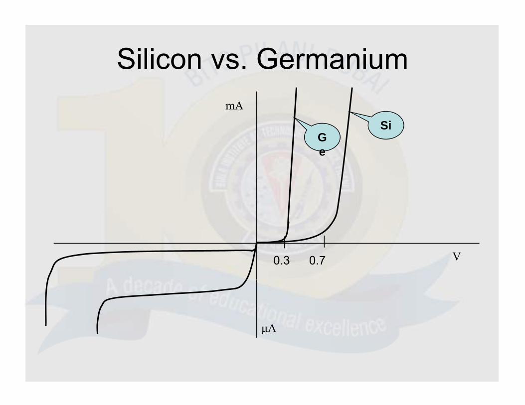
Silicon vs. Germanium
SimA
SiGe
0.3 0.7 V
μAμA
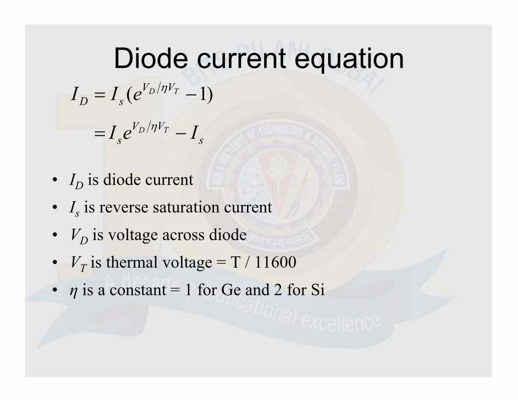
Diode current equation)1( TD VV
sD eII
VV
I i di d t
sVV
s IeI TD
• ID is diode current• Is is reverse saturation current• VD is voltage across diode• VT is thermal voltage = T / 11600• η is a constant = 1 for Ge and 2 for Si

Diode current equation
• For positive values of VD (forward bias), the first term growsFor positive values of VD (forward bias), the first term grows quickly and overpowers the second term. So,
TD VVeII
• For large negative values of VD (reverse bias), the first term
sD eII
g g D ( )drops much below the second term. So, ID ≈ –Is
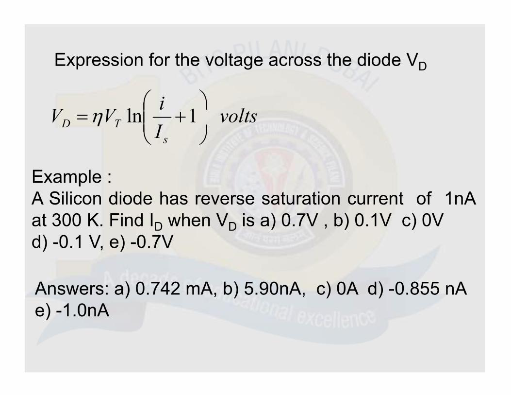
Expression for the voltage across the diode VD
voltsiVV TD
1lnIs
TD
E lExample : A Silicon diode has reverse saturation current of 1nAat 300 K Find ID when VD is a) 0 7V b) 0 1V c) 0Vat 300 K. Find ID when VD is a) 0.7V , b) 0.1V c) 0Vd) -0.1 V, e) -0.7V
Answers: a) 0.742 mA, b) 5.90nA, c) 0A d) -0.855 nA e) -1.0nA

Example :A Silicon diode has a saturation current of 5nA at 300 KA Silicon diode has a saturation current of 5nA at 300 K a)Find the current for the case that the forward bias
voltage is 0.7Vvoltage is 0.7Vb)Find the forward bias voltage that results in a current
of 15 mA
c) Find the value of Resistance Rin the following circuit , when thein the following circuit , when theis 15 mA
←---VD---→← VD →
Ans: a) 3.71 mA, b) 0.772 Vc) R=3.49 Ω
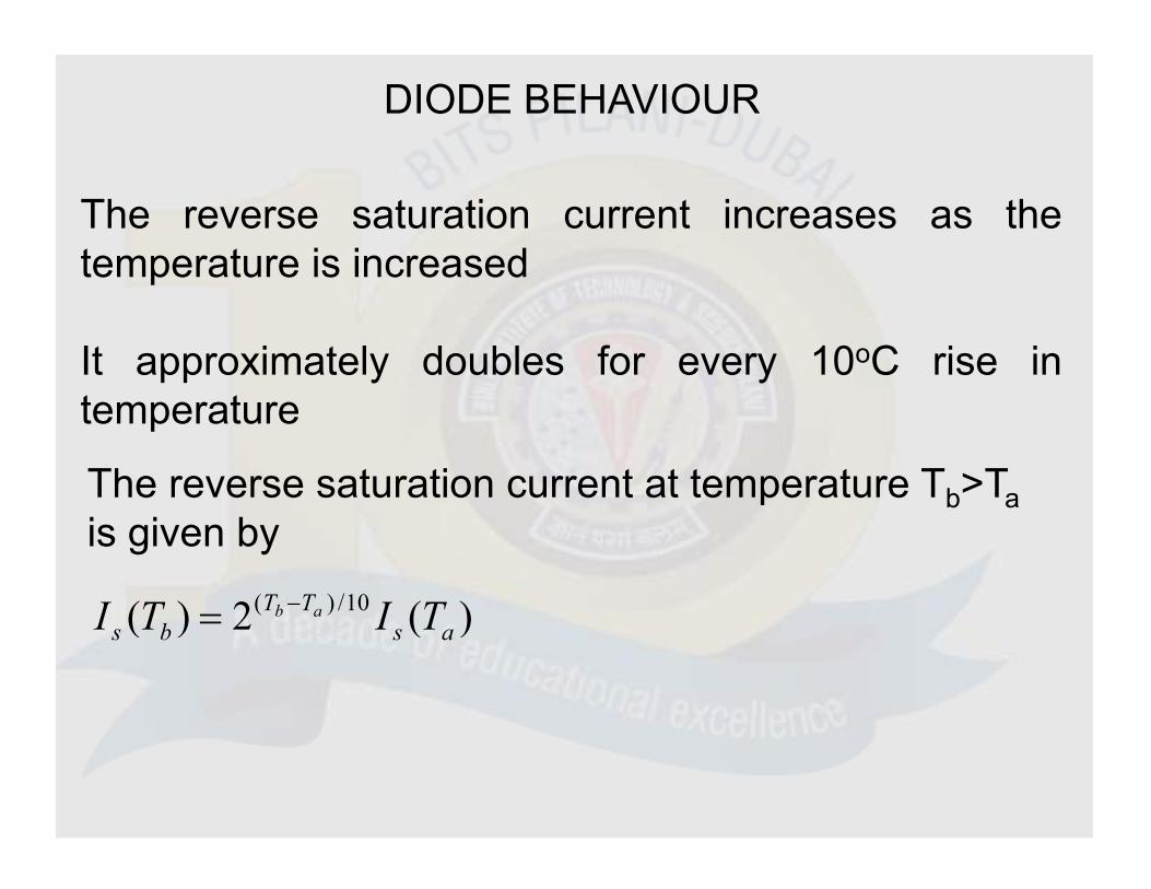
DIODE BEHAVIOUR
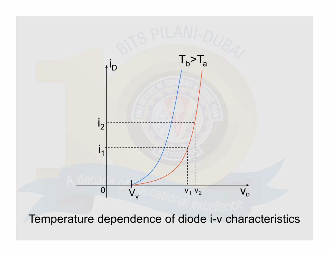
The reverse saturation current increases as thetemperature is increasedtemperature is increased
It approximately doubles for every 10oC rise intemperature
The reverse saturation current at temperature Tb>Tap b ais given by
)(2)( 10/)( TT TITI ab )(2)( )(asbs TITI ab
iD Tb>Ta
i2
i1
vD0 Vγ
v1 v2
Temperature dependence of diode i-v characteristics

Example:Given that the current through a IN4153 siliconGiven that the current through a IN4153 silicondiode is 10 mA, find the voltage across the diodewhen the temperature is a) 290 K b) 310 K c) 320 Kwhen the temperature is a) 290 K b) 310 K c) 320 KReverse saturation current at 300 k is 10 nA
Ans: a) 0.726 V b) 0.70 V c) 0.687 V
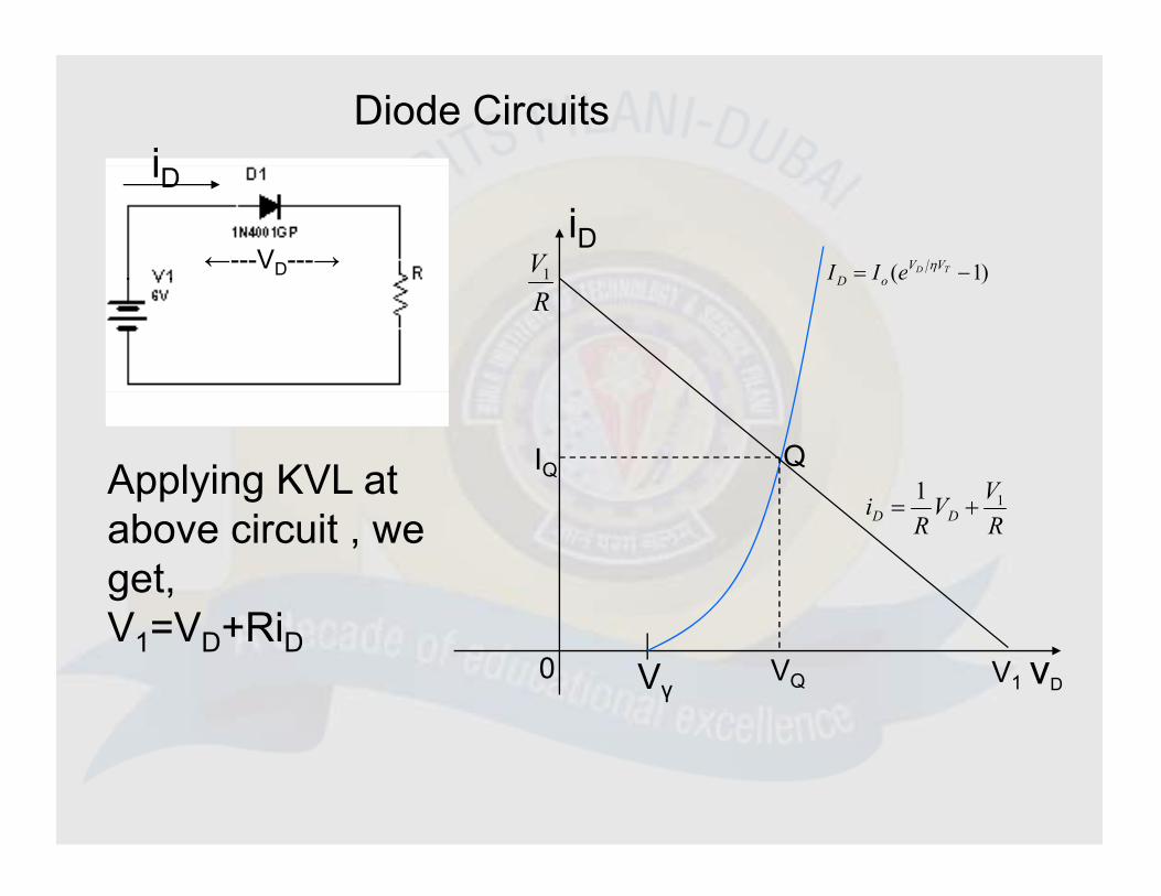
Diode Circuits i
iDV1 )1( TD VV
D eII ←---VD---→
iD
R1 )1(oD eII
QIQVVi 11
Applying KVL at
RVR
i DD1
above circuit , we get,V V +Ri
vD0 Vγ V1VQ
V1=VD+RiD
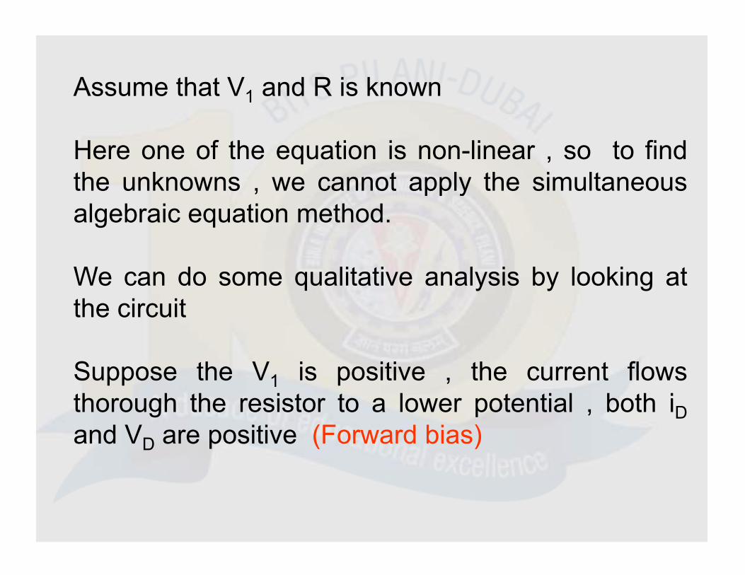
Assume that V1 and R is known
Here one of the equation is non-linear , so to findthe unknowns we cannot apply the simultaneousthe unknowns , we cannot apply the simultaneousalgebraic equation method.
We can do some qualitative analysis by looking atthe circuit
Suppose the V1 is positive , the current flowsth h th i t t l t ti l b th ithorough the resistor to a lower potential , both iDand VD are positive (Forward bias)
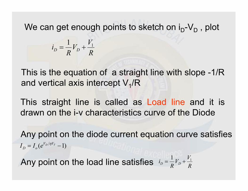
We can get enough points to sketch on iD-VD , plot
RVV
Ri DD
11
This is the equation of a straight line with slope -1/R and vertical axis intercept V /Rand vertical axis intercept V1/R
This straight line is called as Load line and it isdrawn on the i-v characteristics curve of the Diode
A i t th di d t ti ti fiAny point on the diode current equation curve satisfies )1( TD VV
oD eII
V1Any point on the load line satisfies RVV
Ri DD
11
The intersection of both the curve will satisfy boththe equations simultaneously and that point is calledthe equations simultaneously and that point is calledas quiescent point (Operating point)
Thus solution to the equations IQ and VQ is obtainedgraphically , instead of analytically
Example : Suppose that for the diode circuit shownExample : Suppose that for the diode circuit shownV1=9V , R= 2KΩ, and the silicon diode has thesaturation current of 5nA at 300 K. Determine ID andDVD ( Begin by using VD=0.5 V)
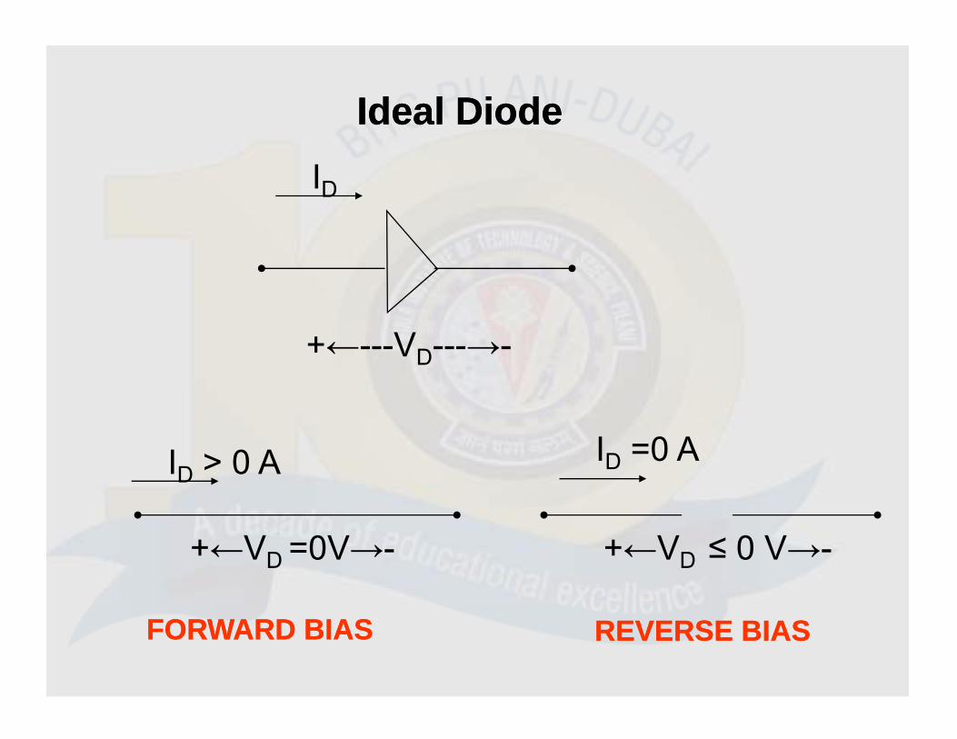
Ideal DiodeIdeal DiodeID
+←---VD---→-
ID > 0 A ID =0 A
+←VD =0V→- +←VD ≤ 0 V→-
FORWARD BIASFORWARD BIAS REVERSE BIASREVERSE BIAS
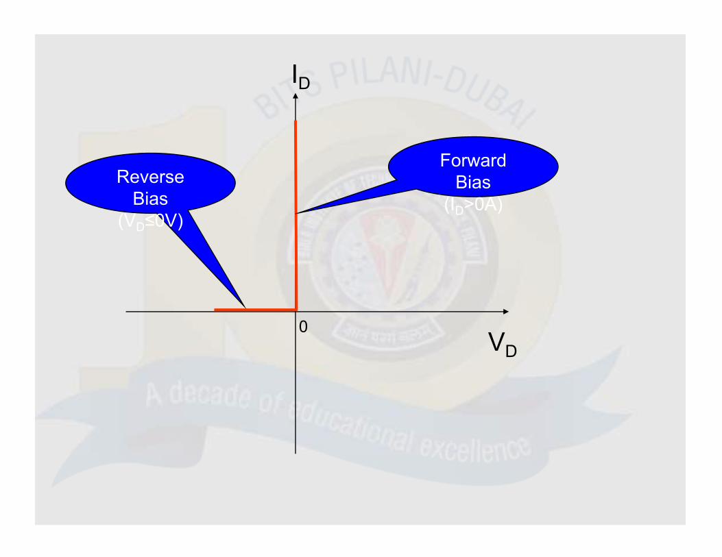
ID
Forward Re erse Bias
(ID>0A)Reverse
Bias(VD≤0V)
VD0

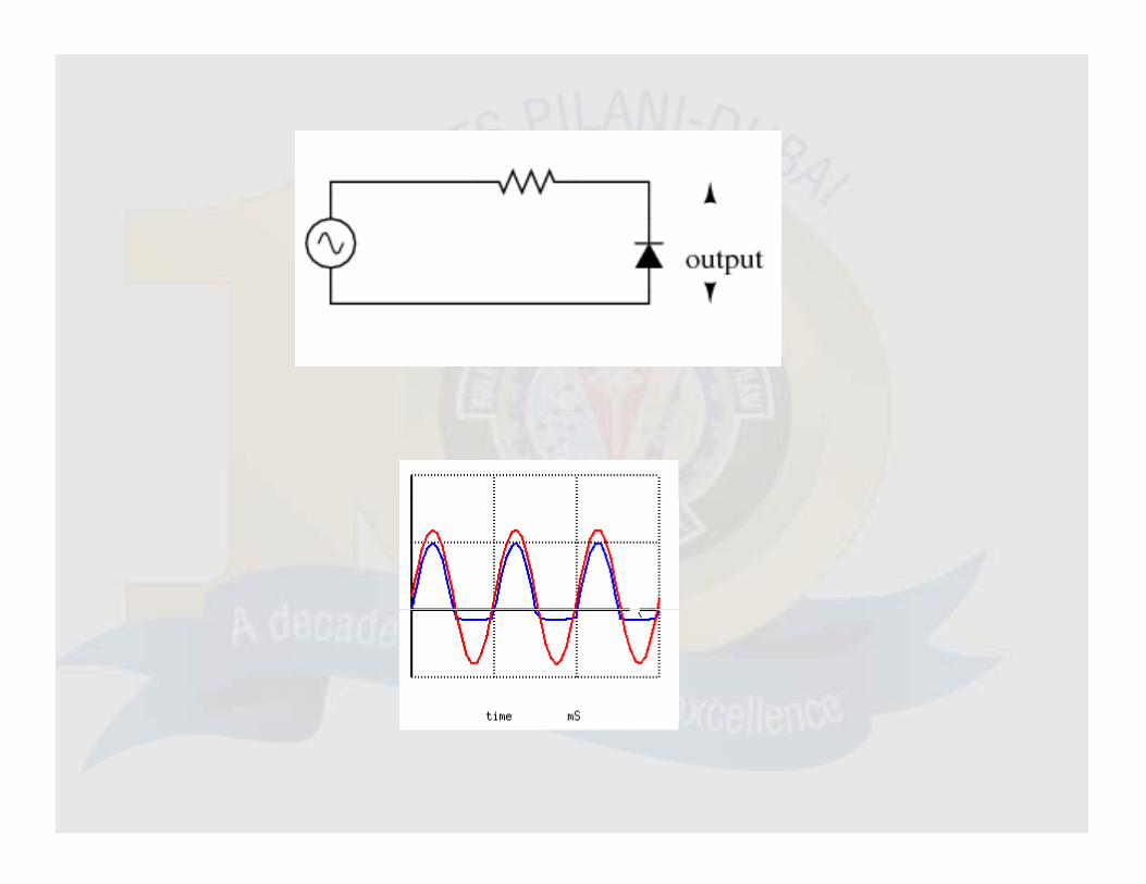
Half wave rectifierHalf wave rectifier
+ v - + v=0V -
i=0
+ v -
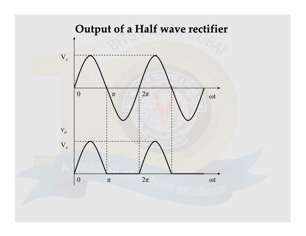
Output of a Half wave rectifierOutput of a Half wave rectifier
Vs
ωt0 π 2π
voo
Vs
ωt0 π 2π