Chapter 7. The pn Junction
15
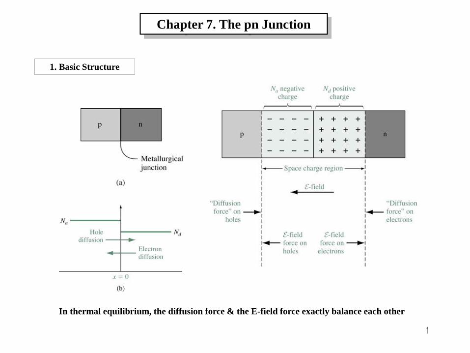
1 Chapter 7. The pn Junction 1. Basic Structure In thermal equilibrium, the diffusion force & the E-field force exactly balance each other
Transcript of Chapter 7. The pn Junction
1
Chapter 7. The pn Junction
1. Basic Structure
In thermal equilibrium, the diffusion force & the E-field force exactly balance each other
2
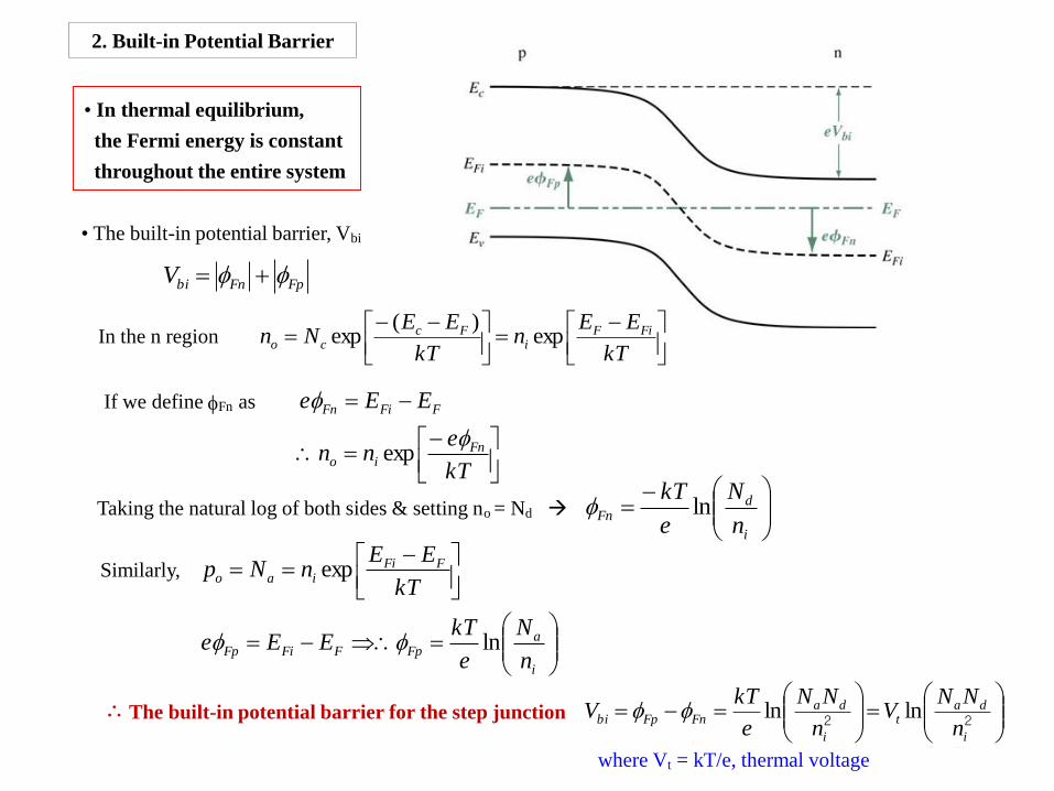
2. Built-in Potential Barrier
• In thermal equilibrium,
the Fermi energy is constant
throughout the entire system
• The built-in potential barrier, Vbi
FpFnbiV
kT
EEn
kT
EENn FiF
iFc
co exp)(
exp
kT
enn
EEe
Fnio
FFiFn
exp
i
dFn
n
N
e
kTln
i
aFpFFiFp
FFiiao
n
N
e
kTEEe
kT
EEnNp
ln
exp
In the n region
If we define Fn as
Taking the natural log of both sides & setting no = Nd
Similarly,
∴ The built-in potential barrier for the step junction
22i
dat
i
daFnFpbi
n
NNV
n
NN
e
kTV lnln
where Vt = kT/e, thermal voltage
3
dx
xdEx
dx
xd
s
)()()(2
2
1
)(Cx
eNdx
eNdx
xE
s
a
s
a
s
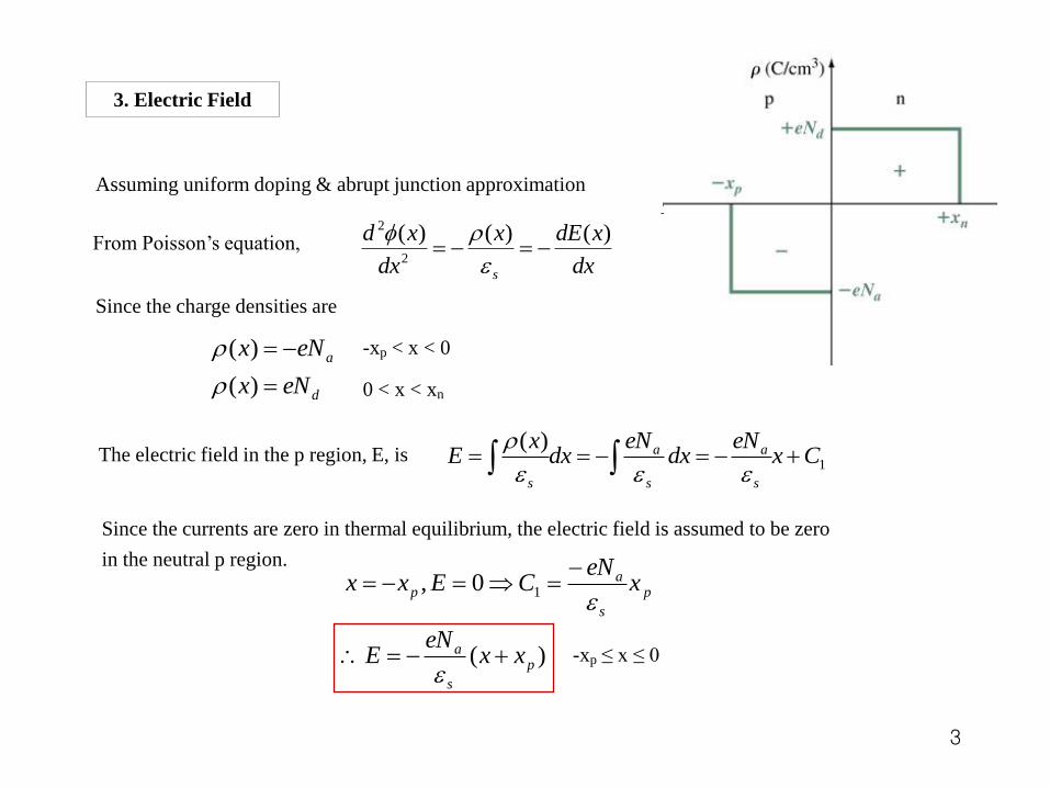
3. Electric Field
Assuming uniform doping & abrupt junction approximation
d
a
eNx
eNx
)(
)(
)(
0, 1
p
s
a
p
s
ap
xxeN
E
xeN
CExx
From Poisson’s equation,
dx
xdEx
dx
xd
s
)()()(2
2
Since the charge densities are
-xp < x < 0
0 < x < xn
The electric field in the p region, E, is
Since the currents are zero in thermal equilibrium, the electric field is assumed to be zero
in the neutral p region.
-xp ≤ x ≤ 0

4
In the n region,
Since E=0 at x=xn, C2=-eNdxn/s
The electric field is continuous at x=0
2CxeN
dxeN
Es
d
s
d
)( n
s
d xxeN
E
ndpa
n
s
dp
s
a
xNxN
xeN
xeN
)(
0 ≤ x ≤ xn
5
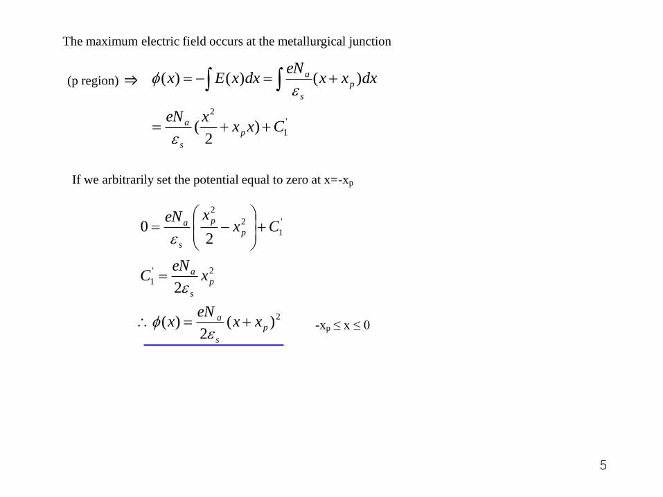
The maximum electric field occurs at the metallurgical junction
(p region) ⇒
'
1
2
)2
(
)()()(
CxxxeN
dxxxeN
dxxEx
p
s
a
p
s
a
If we arbitrarily set the potential equal to zero at x=-xp
2
2'
1
'
1
2
2
)(2
)(
2
20
p
s
a
p
s
a
p
p
s
a
xxeN
x
xeN
C
CxxeN
-xp ≤ x ≤ 0
6
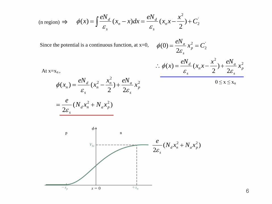
Since the potential is a continuous function, at x=0,
At x=xn ,
22
'
2
2
2)
2()(
2)0(
p
s
an
s
d
p
s
a
xeNx
xxeN
x
CxeN
)(2
2)
2()(
22
22
2
pand
s
p
s
ann
s
dn
xNxNe
xeNx
xeN
x
0 ≤ x ≤ xn
(n region) ⇒ '
2
2
)2
()()( Cx
xxeN
dxxxeN
x n
s
dn
s
d
)(2
22
pand
s
xNxNe
7
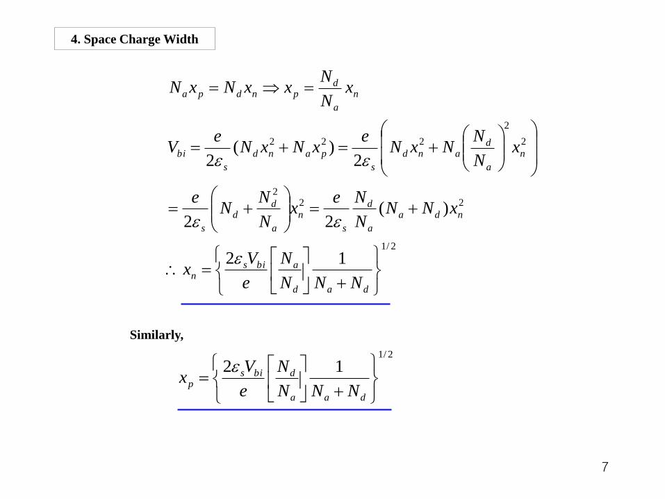
4. Space Charge Width
2/1
222
2
2
222
12
)(22
2)(
2
dad
abisn
nda
a
d
s
n
a
dd
s
n
a
dand
s
pand
s
bi
n
a
dpndpa
NNN
N
e
Vx
xNNN
Nex
N
NN
e
xN
NNxN
exNxN
eV
xN
NxxNxN
Similarly,
2/1
12
daa
dbisp
NNN
N
e
Vx
8
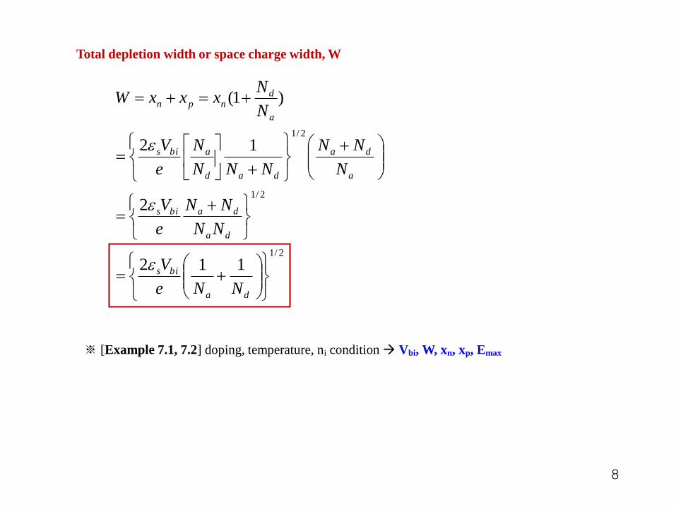
Total depletion width or space charge width, W
2/1
2/1
2/1
112
2
12
)1(
da
bis
da
dabis
a
da
dad
abis
a
dnpn
NNe
V
NN
NN
e
V
N
NN
NNN
N
e
V
N
NxxxW
※ [Example 7.1, 7.2] doping, temperature, ni condition Vbi, W, xn, xp, Emax
9
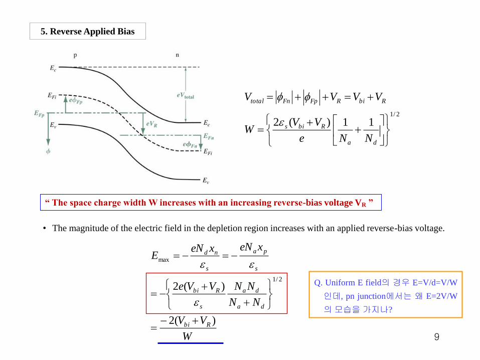
5. Reverse Applied Bias
W
VV
NN
NNVVe
xeNxeNE
Rbi
da
da
s
Rbi
s
pa
s
nd
)(2
)(22/1
max
“ The space charge width W increases with an increasing reverse-bias voltage VR ”
• The magnitude of the electric field in the depletion region increases with an applied reverse-bias voltage.
2/1
11)(2
da
Rbis
RbiRFpFntotal
NNe
VVW
VVVV
Q. Uniform E field의 경우 E=V/d=V/W
인데, pn junction에서는 왜 E=2V/W
의모습을가지나?
10
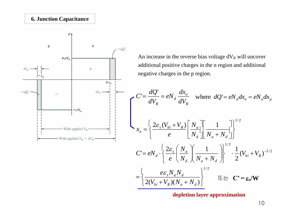
6. Junction Capacitance
An increase in the reverse bias voltage dVR will uncover
additional positive charges in the n region and additional
negative charges in the p region.
2/1
2/1
2/1
2/1
))((2
)(2
112'
1)(2
''
daRbi
das
Rbi
dad
asd
dad
aRbisn
R
nd
R
NNVV
NNe
VVNNN
N
eeNC
NNN
N
e
VVx
dV
dxeN
dV
dQC
depletion layer approximation
또는 C’ = s/W
pand dxeNdxeNdQ ' where
11
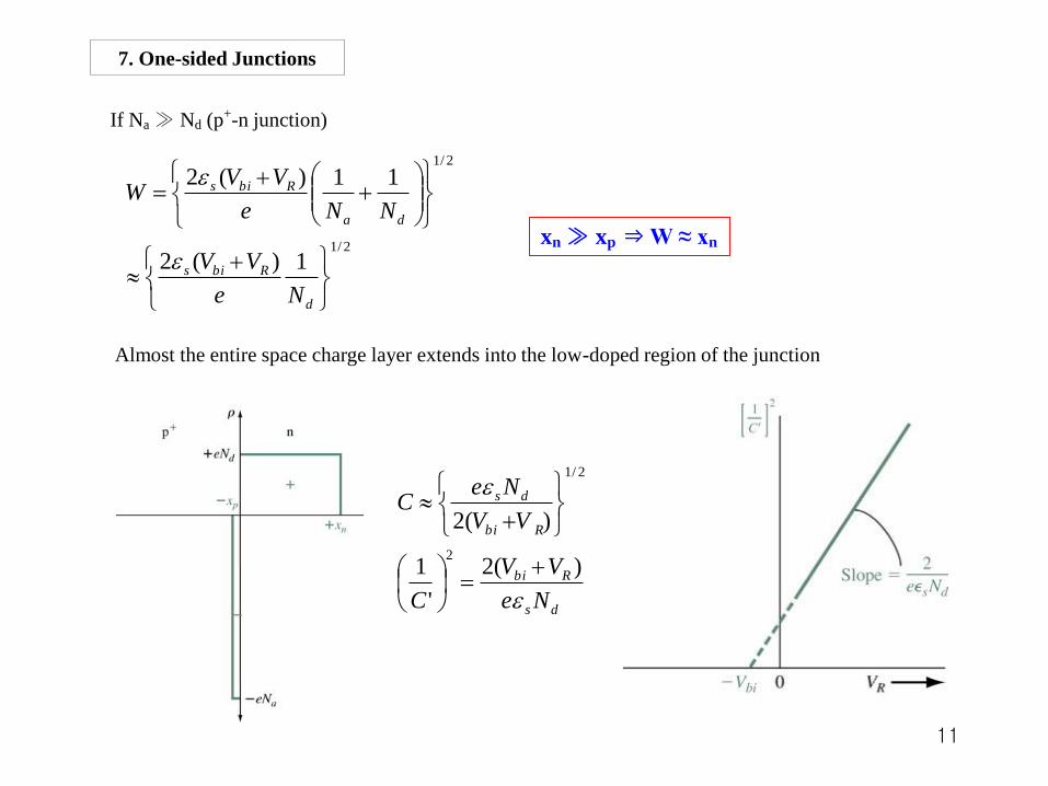
7. One-sided Junctions
If Na≫ Nd (p+-n junction)
2/1
2/1
1)(2
11)(2
d
Rbis
da
Rbis
Ne
VV
NNe
VVW
ds
Rbi
Rbi
ds
Ne
VV
C
VV
NeC
)(2
'
1
)(2
2
2/1
xn≫ xp⇒W ≈ xn
Almost the entire space charge layer extends into the low-doped region of the junction
12
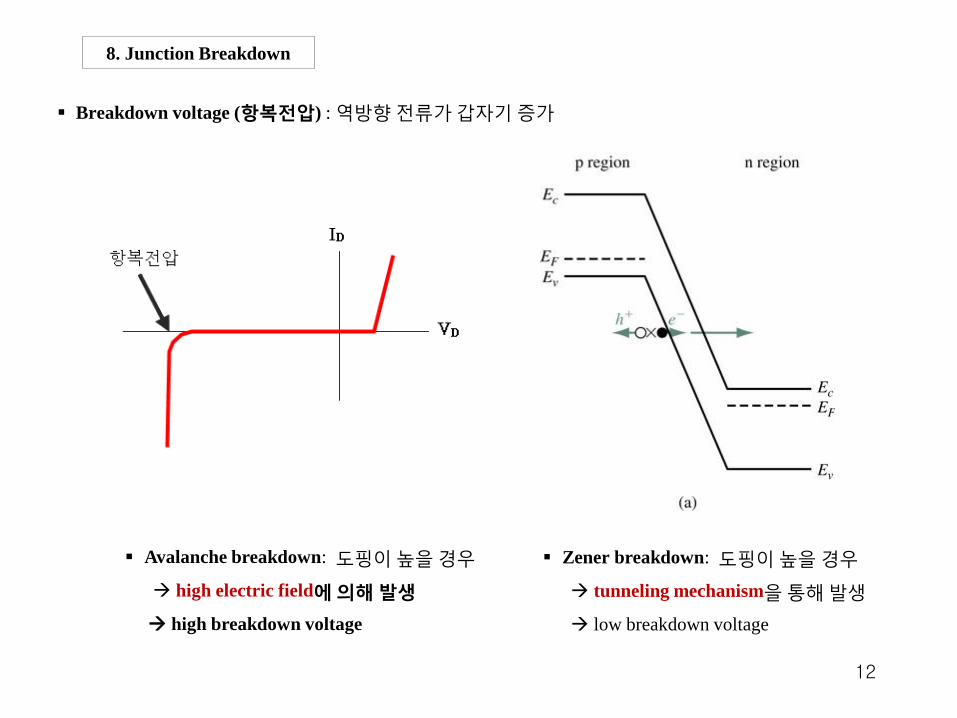
Breakdown voltage (항복전압) : 역방향전류가갑자기증가
8. Junction Breakdown
Zener breakdown: 도핑이높을경우
tunneling mechanism을통해발생
low breakdown voltage
Avalanche breakdown: 도핑이높을경우
high electric field에의해발생
high breakdown voltage

13
Avalanche Breakdown : 공핍영역(depletion region)에서 carrier들의 collision process에의해발생
의미수를의생성되는의해서정공에전자와단위길이당
이온화율이며과
은여기서
과정에서
pair hole-electron
,
factor, tionmultiplica
tionmultiplica Avalanche
정공의전자와는여기서 pn
ppnnn
nonn
nonn
dxxIdxxIxdI
IIM
IMWI
)()()(
)0(
)(
어떤지점 x에서의전류증분

14
0 0
0
0
0
( . 9.28)
11
n
n n p p
n p
n
p n n p
p n
n
W W
n n n
Wn no no
n no
W
n
dI xI x I x
dx
I I x I x
dI xI x I
dx
dI xI
dx
dI x I W I I dx
M I Idx
I
M I I refer to Fig
dxM
로가정하면
이므로
그러므로 avalanche breakdown 전압은
Mn이 ∞에 접근할 때의 전압으로 정의
될 수 있으므로 avalanche breakdown
조건은다음과같이표현될수있음
01
W
dx
15
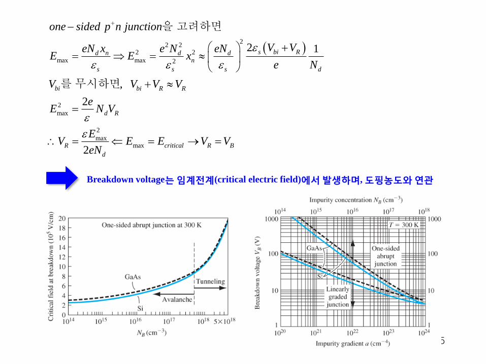
2
2 22 2
max max 2
2
max
2
maxmax
2 1
,
2
2
s bi Rd n d dn
s s s d
bi bi R R
d R
R critical R B
d
one sided p n junction
V VeN x e N eNE E x
e N
V V V V
eE N V
EV E E V V
eN
을고려하면
를무시하면
Breakdown voltage는임계전계(critical electric field)에서발생하며, 도핑농도와연관