Unit-II Physics of Semiconductor Devices. Formation of PN Junction and working of PN junction....
28
Unit-II Physics of Semiconductor Devices
-
Upload
emerald-booker -
Category
Documents
-
view
225 -
download
0
Transcript of Unit-II Physics of Semiconductor Devices. Formation of PN Junction and working of PN junction....

Unit-II
Physics of Semiconductor Devices
Formation of PN Junction and working of PN junction. Energy Diagram of PN Diode, I-V Characteristics of PN Junction, LED, Solar cell, applications.

Introduction In electronics a diode is a two- terminal electronic
component with asymmetric conductance; it has low (ideally zero) resistance to current in one direction, and high (ideally infinite) resistance in the other.
Thermionic (Vacuum tubes) diodes and solid state (semiconductor) diodes were developed separately, at approximately the same time, in the early 1900s, as radio receiver detectors.
Indian scientist Jagadish Chandra Bose was the first to use a crystal for detecting radio waves in 1894

Until the 1950s vacuum tube diodes were more often used in radios because the early point-contact type semiconductor diodes (cat's-whisker detectors) were less stable, and because most receiving sets had vacuum tubes for amplification that could easily have diodes included in the tube (for example the 12SQ7 double diode triode), and vacuum tube rectifiers and gas-filled rectifiers handled some high voltage/high current rectification tasks beyond the capabilities of semiconductor diodes (such as selenium rectifiers) available at the time.
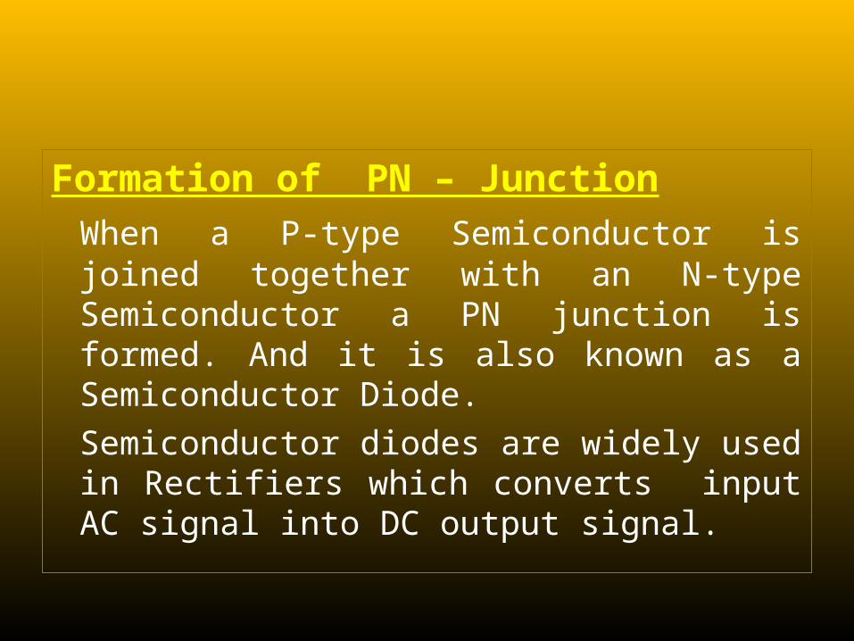
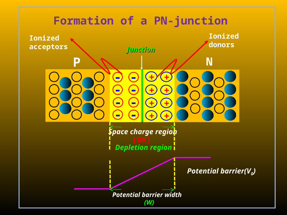
Formation of PN – Junction
When a P-type Semiconductor is joined together with an N-type Semiconductor a PN junction is formed. And it is also known as a Semiconductor Diode.
Semiconductor diodes are widely used in Rectifiers which converts input AC signal into DC output signal.
P N----
---- +
+++
+
+++
Space charge region(OR)
Depletion region
JunctionJunction
Ionized acceptors
Ionized donors
Potential barrier(V0)
Potential barrier width (W)(W)
Formation of a PN-junction
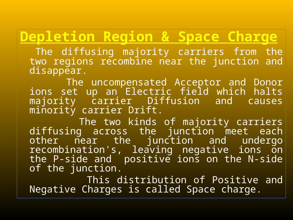
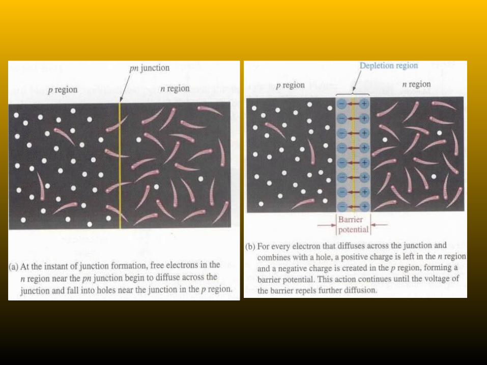
Depletion Region & Space Charge The diffusing majority carriers from the two regions recombine near the junction and disappear.
The uncompensated Acceptor and Donor ions set up an Electric field which halts majority carrier Diffusion and causes minority carrier Drift. The two kinds of majority carriers diffusing across the junction meet each other near the junction and undergo recombination's, leaving negative ions on the P-side and positive ions on the N-side of the junction.
This distribution of Positive and Negative Charges is called Space charge.

N P
CathodeAnode
_+
Diode Symbol

Energy Diagram of PN Diode

Fermi level
Depletion regionPN - junction
EFn
Valence band
Conduction band
NP
EFp
E
eVB
eVB
Ev
Ec
Ev
Ec
Un Biased

Fermi level
Depletion regionPN - junction
EFn
Valence band
Conduction band
NP
EFp
E
eVB
eVB
Ev
Ec
Ev
Ec
Forward Bias
eVF

Fermi level
Depletion regionPN - junction
EFn
Valence band
Conduction band
NP
EFp
E
eVB
eVB
Ev
Ec
Ev
Ec
Reverse Bias
eVR

V - I Characteristics of PN Junction:
The diode can be operated in two different ways, as Forward and Reverse bias.
When positive terminal of the battery is connected to the P-type & negative terminal is to the N-type of the PN-junction diode, known the diode is kept in forward bias.
When negative terminal of the battery is connected to the P-type & positive terminal is to the N-type of the PN-junction diode, known the diode is kept in reverse bias.
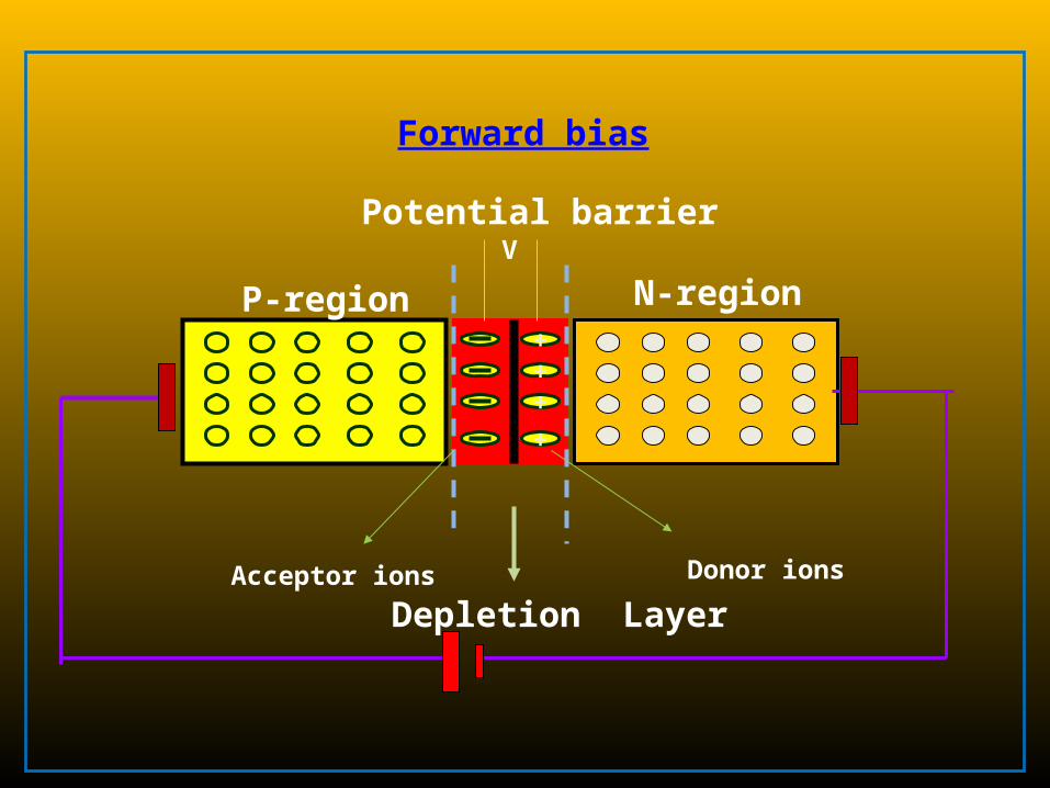
Depletion Layer
N-regionP-region+++
+
Donor ionsAcceptor ions
VPotential barrier
Forward bias
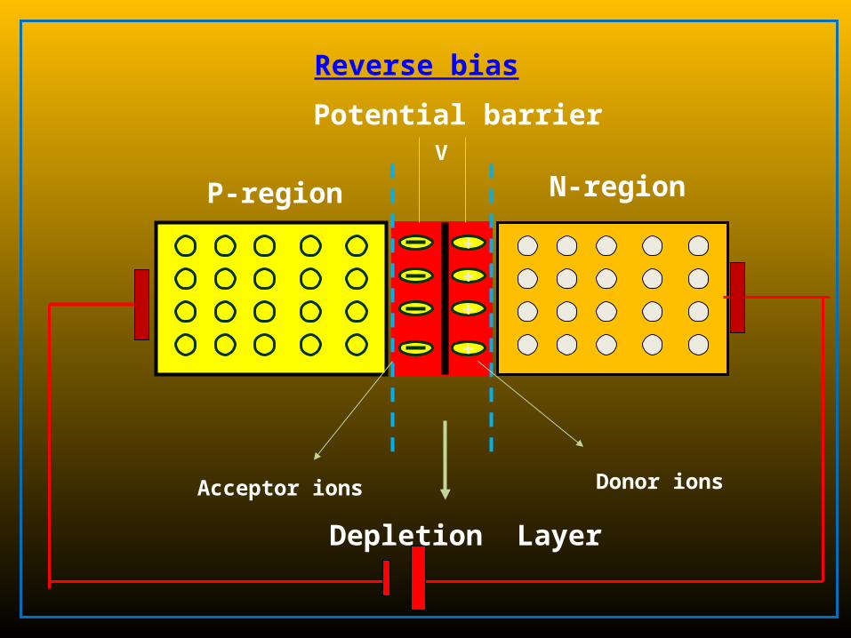
Depletion Layer
N-regionP-region
+
+
+
+
Donor ionsAcceptor ions
V
Potential barrier
Reverse bias

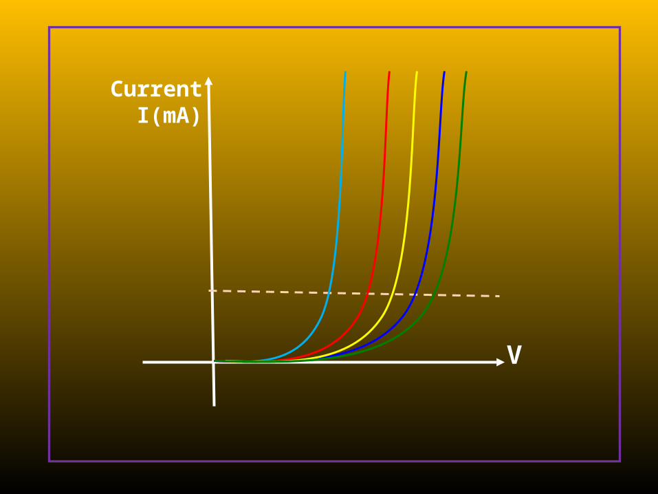
Forward Bias
Reverse Bias V
I
Current
Reverse break down current
Forward Current
Knee Voltage
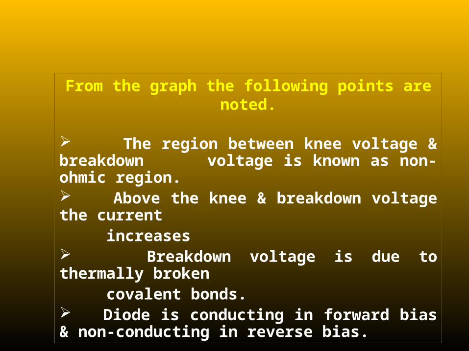
From the graph the following points are noted.
The region between knee voltage & breakdown voltage is known as non-ohmic region. Above the knee & breakdown voltage the current increases Breakdown voltage is due to thermally broken covalent bonds. Diode is conducting in forward bias & non-conducting in reverse bias.

Light emitting diode (LED) LED is a semiconductor PN-junction diode which converts electrical energy to light under forward biasing. It emits light in both visible & IR region.
NOTE:
LEDs are typically made of compound semiconductors (OR) direct band gap semiconductors like gallium arsenide.
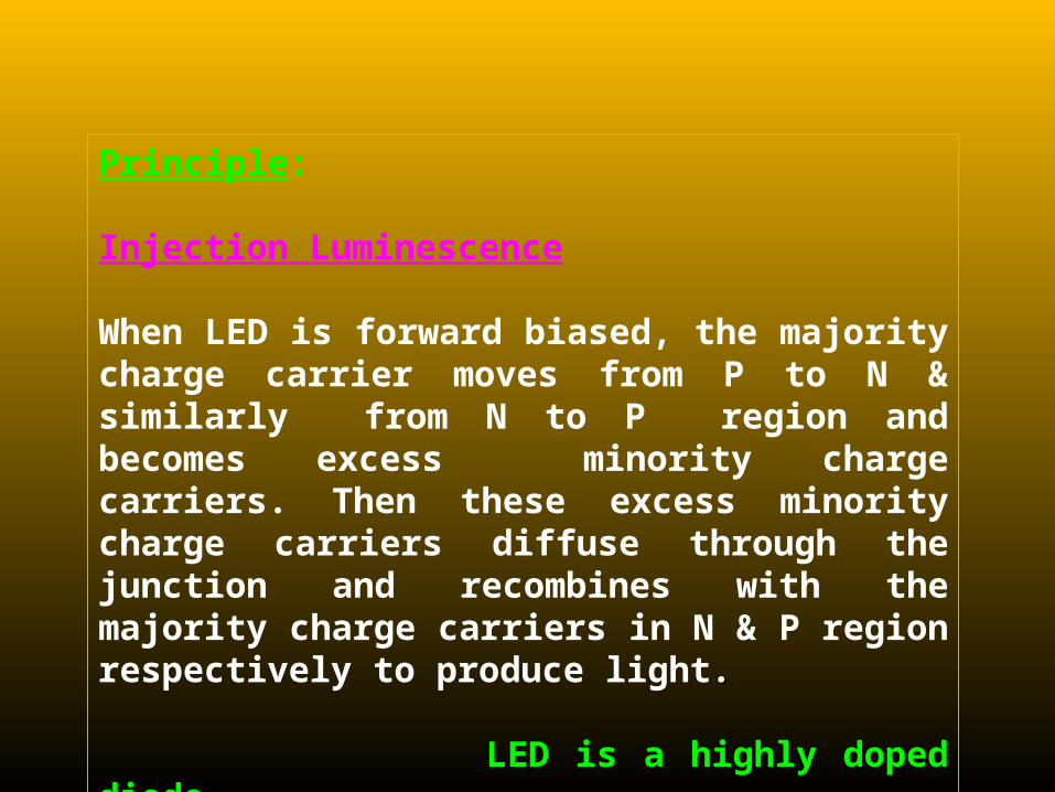
Principle:
Injection Luminescence
When LED is forward biased, the majority charge carrier moves from P to N & similarly from N to P region and becomes excess minority charge carriers. Then these excess minority charge carriers diffuse through the junction and recombines with the majority charge carriers in N & P region respectively to produce light..
LED is a highly doped diode

substrate
VF
N
POhmicContacts(Al)
Sio2
Photons

The PN-junction is made by doping silicon by GaAs crystal. Here silicon can act both as donor & acceptor.
Therefore, a shallow PN-junction is formed on GaAs substrate such that P-layer is formed by diffusion on N-layer as shown in figure.
In order to increase the probability of radiative recombination's, the thickness of the N-layer is taken higher than that of the thickness of the P-layer.
The top layer of the P material is left uncovered for the emission of light.

Working:
If the diode is properly biased the charge carriers move across the junction. If the biasing voltage is further increased, these excess minority carriers diffuse away from the junction and directly recombine with the majority carriers.. Therefore, electron-hole recombination occurs more & more and thereby light is emitted through the top layer of the P-material which is left uncovered as shown in figure.

+ -
CathodeAnode
Cathode
Anode
LED SYMBOL
V
Current I(mA)


1)exp(0
KT
eVII

![$$ 5 - . 1 ) $ · ... PN junction, Junction Theory, VI characteristics of PN junction diode, Ideal diode, Static and Dynamic Resistance [1][2], Diode current equation[2],Diode notations](https://static.fdocuments.in/doc/165x107/5ae6f8997f8b9a29048e3147/-5-1-pn-junction-junction-theory-vi-characteristics-of-pn-junction.jpg)