PN-JUNCTION DIODE AND DIODE CIRCUITSj.guntzel/ine5442/pn-junction.pdf · Electronics 2 PN-JUNCTION...
31
Electronics 1 PN-JUNCTION DIODE AND DIODE CIRCUITS Objectives Understand the basic principles of diode operation and the current- voltage exponential characteristic; Use equivalent models of diodes to analyze typical diode circuits Analyze and determine experimentally the characteristics of typical diode circuits; Use circuit simulator to analyze diode applications.
Transcript of PN-JUNCTION DIODE AND DIODE CIRCUITSj.guntzel/ine5442/pn-junction.pdf · Electronics 2 PN-JUNCTION...
Electronics1
PN-JUNCTION DIODE AND
DIODE CIRCUITS
Objectives
Understand the basic principles of diode operation and the current-
voltage exponential characteristic;
Use equivalent models of diodes to analyze typical diode circuits
Analyze and determine experimentally the characteristics of
typical diode circuits;
Use circuit simulator to analyze diode applications.
Electronics2
PN-JUNCTION DIODE AND
DIODE CIRCUITS
1 Main properties of semiconductors
2 The PN-junction in Equilibrium
3 The i – v Characteristics of the PN-Junction
4 Deviations from the Ideal Diode
5 Analysis of the Diode Circuits
6 Rectifier Circuits
Electronics3

Electronics4
Electronics5

Electronics6
Electronics7
Electronics8
Electronics9
Electronics10
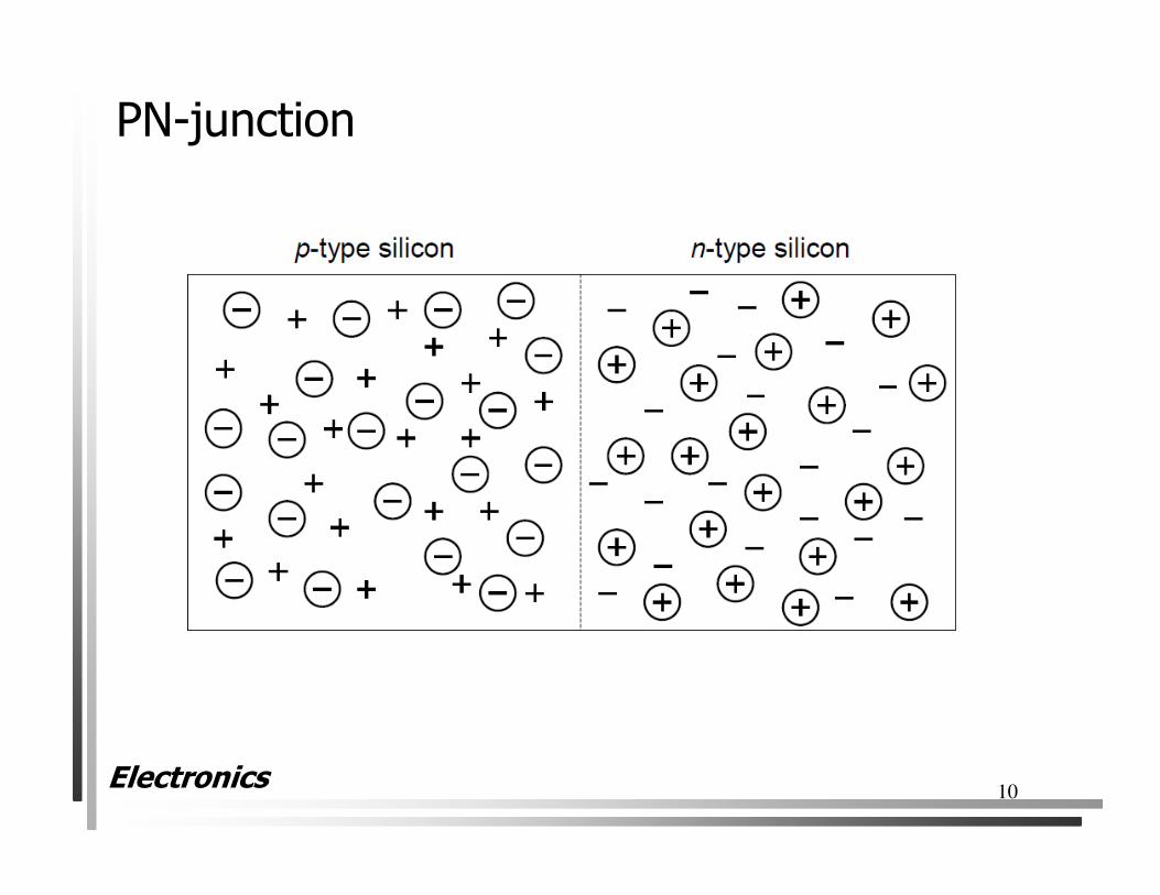
PN-junction

Electronics11
1016
1014
1012
1010
106
108
104
102
nn = ND
pp = NA
np = ni2 / NA pn = ni
2/ ND
N A=1016
cm-3
PN D=10
15cm
-3
N
ohmic
contact
ohmic
contact
A B
-N A
N D
x(a) Step junction
(b) “initial” carrier concentrations
ni=1010cm-3
“Before contacting”, the two
regions are electrically neutral
( ρ = 0 ).
Electronics12
Electronics13
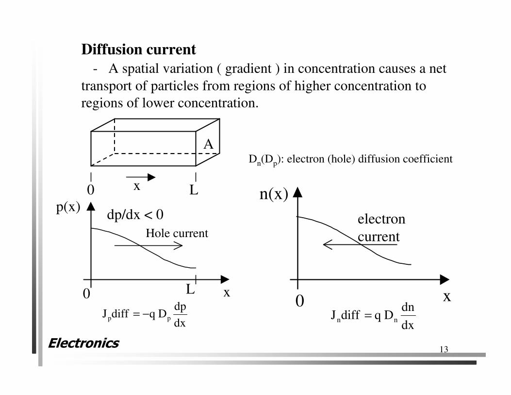
Diffusion current
- A spatial variation ( gradient ) in concentration causes a net
transport of particles from regions of higher concentration to
regions of lower concentration.
0 L x
Hole current
p(x)
A
0 L x
dp/dx < 0 electron
current
n(x)
0 x
dx
dp DqdiffJ pp −=
dx
dn DqdiffJ nn =
Dn(Dp): electron (hole) diffusion coefficient
Electronics14
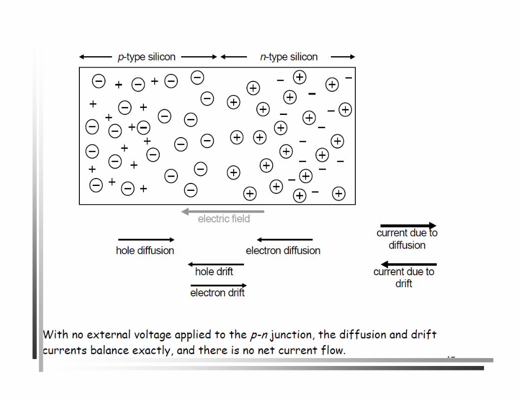
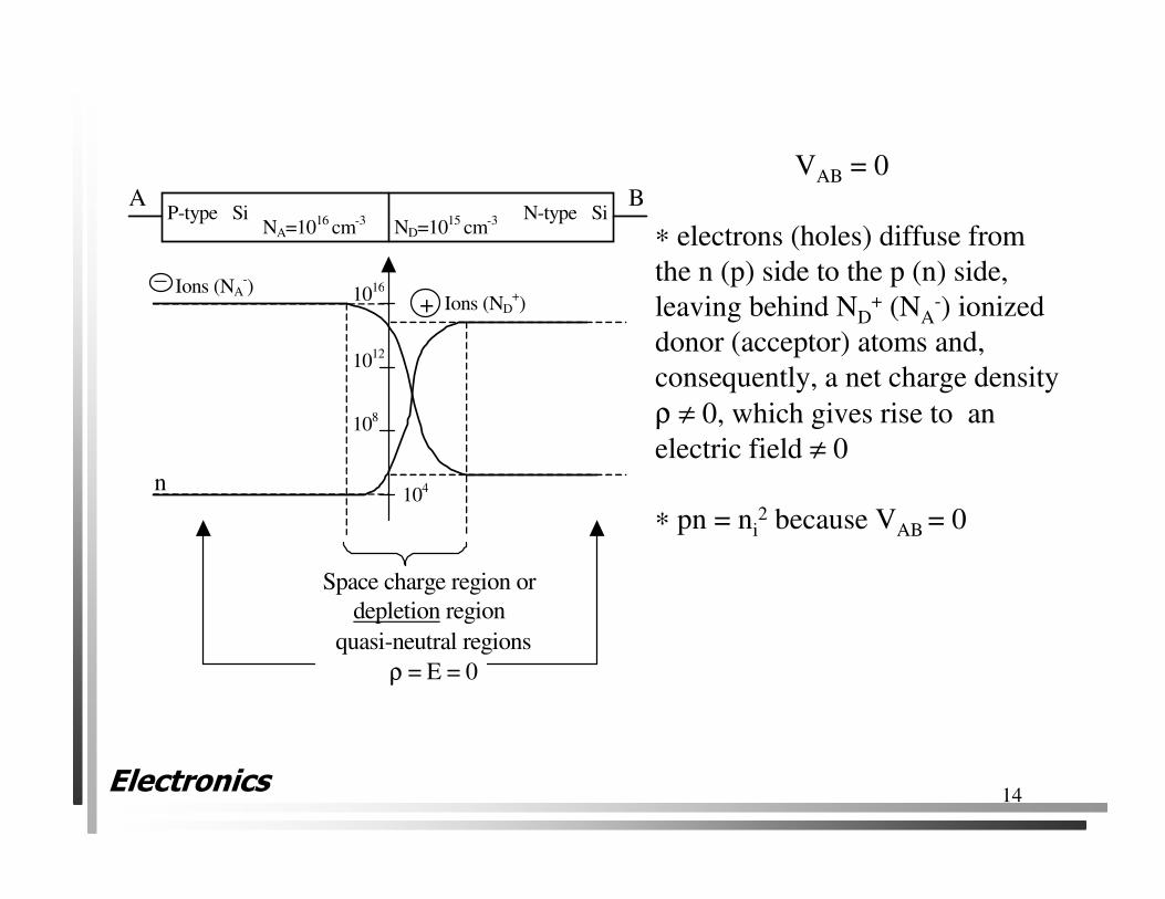
NA=1016 cm-3 ND=1015 cm-3 P-type Si N-type Si
A B
1016
1012
108
104 n
Space charge region or
depletion region
quasi-neutral regions
ρ = E = 0
Ions (NA-)
Ions (ND+) +
_
VAB = 0
∗ electrons (holes) diffuse from
the n (p) side to the p (n) side,
leaving behind ND+ (NA
-) ionized
donor (acceptor) atoms and,
consequently, a net charge density
ρ ≠ 0, which gives rise to an
electric field ≠ 0
∗ pn = ni2 because VAB = 0
Electronics15
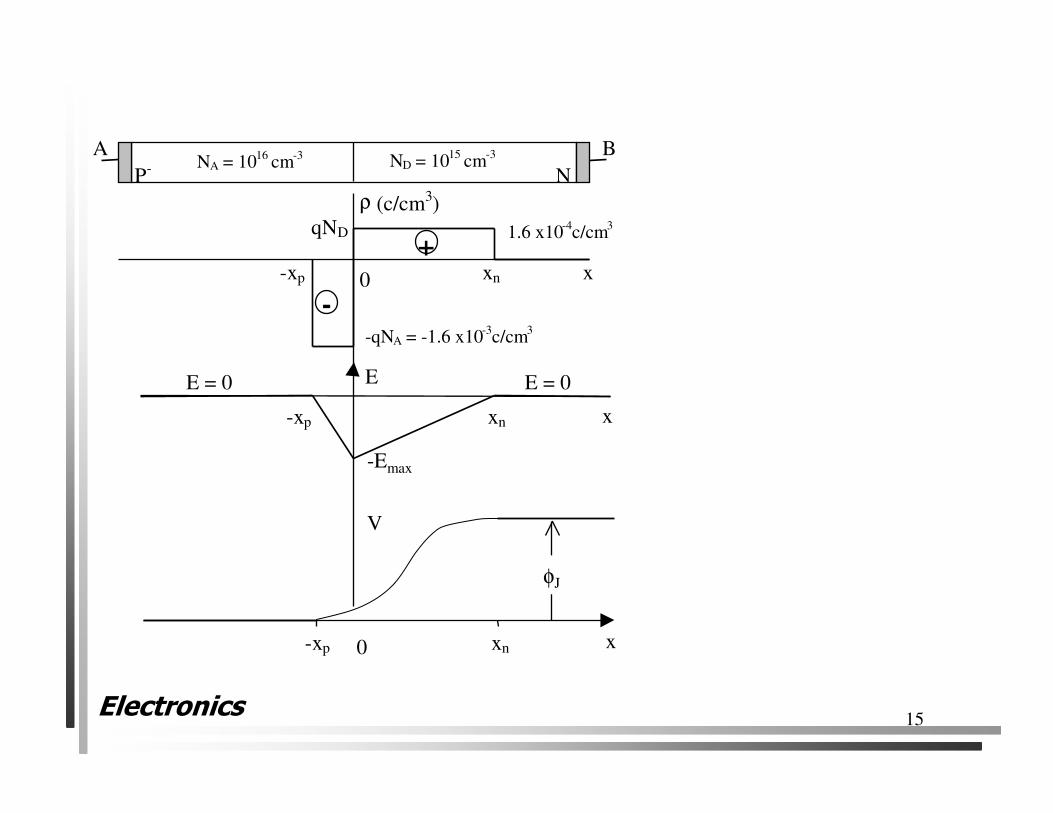
EE = 0 E = 0
-xp xn
-Emax
-xp xn
-qNA = -1.6 x10⁻³
c/cm3
x
x
1.6 x10-4
c/cm3qND
ρ (c/cm3)
+
-
P- NNA = 10
16 cm
-3 ND = 1015
cm-3A B
0
x
φJ
xn-xp 0
V
Electronics16
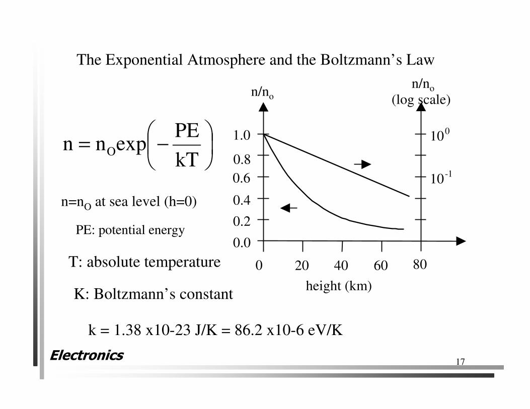
Electronics17
−=
kT
PEexpnn O
PE: potential energy
n=nO at sea level (h=0)
0 20 40 60 80
10-1
100
0.0
0.2
0.4
0.6
0.8
1.0
n/no (log scale)
height (km)
n/no
The Exponential Atmosphere and the Boltzmann’s Law
k = 1.38 x10⁻²³ J/K = 86.2 x10⁻⁶ eV/K
T: absolute temperature
K: Boltzmann’s constant
Electronics18
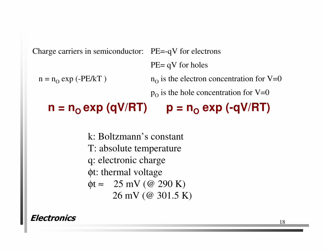
Charge carriers in semiconductor: PE=-qV for electrons
PE= qV for holes
n = nO exp (-PE/kT ) nO is the electron concentration for V=0
pO is the hole concentration for V=0
n = nO exp (qV/RT) p = nO exp (-qV/RT)
k: Boltzmann’s constant
T: absolute temperature
q: electronic charge
φt: thermal voltage
φt ≈ 25 mV (@ 290 K)
26 mV (@ 301.5 K)
Electronics19
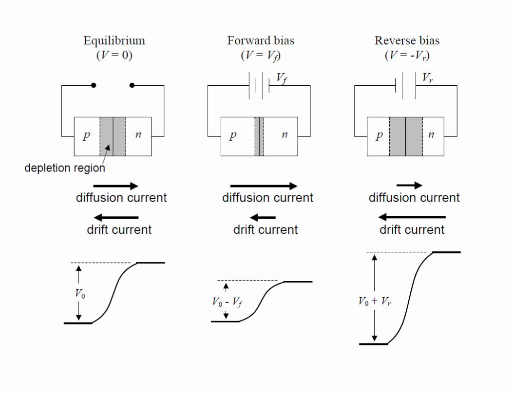
x
φ (x)
xn
-x p
v = 0D
v > 0D
v < 0D
- vD
φj
+ -P-side N-side
+ vD -
Electrostatic junction potential for different applied voltages
Barrier potential = ( φJ - vD )
is controlled by the applied
voltage.
Carrier concentration depends
exponentially on barrier potential
( as in the Boltzmann’s
atmosphere ).
Electronics20
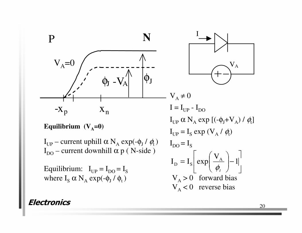
I
VA
VA ≠ 0
I = IUP - IDO
IUP α NA exp [(-φJ+VA) / φt]
IUP = IS exp (VA / φt)
IDO = IS
−
= 1
VexpII A
SD
tφ
VA > 0 forward bias
VA < 0 reverse bias
IUP – current uphill α NA exp(-φJ / φt )
IDO – current downhill α p ( N-side )
Equilibrium: IUP = IDO = IS
where IS α NA exp(-φJ / φt )
P N
φJφJ -VA
-xp
VA=0
xn
Equilibrium (VA=0)
Electronics21
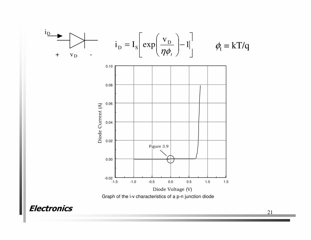
1.51.00.50.0-0.5-1.0-1.5-0.02
0.00
0.02
0.04
0.06
0.08
0.10
Diode Voltage (V)
Diode Current (A)
Figure 3.9
Graph of the i-v characteristics of a p-n junction diode
+ vD -
iD
−
= 1
vexpIi D
SD
tηφ
φt = kT/q
Electronics22
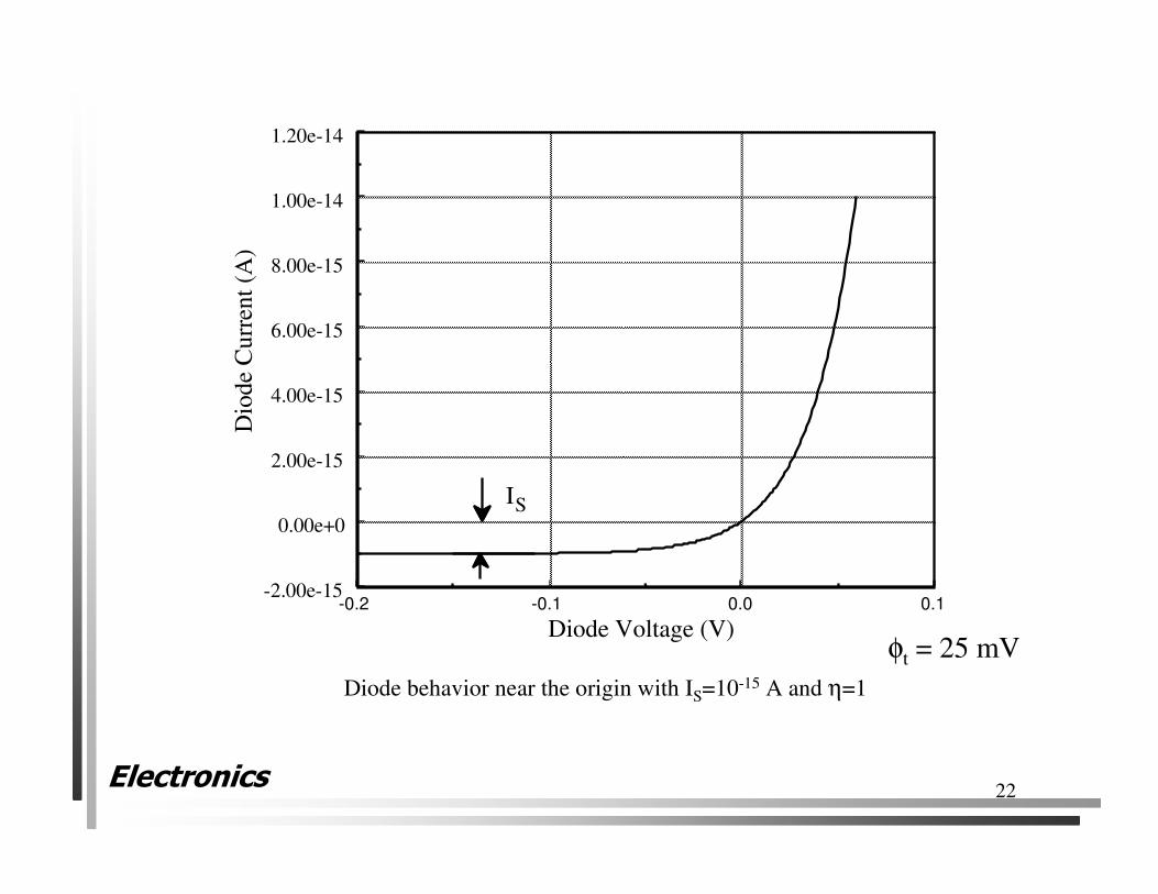
0.10.0-0.1-0.2-2.00e-15
0.00e+0
2.00e-15
4.00e-15
6.00e-15
8.00e-15
1.00e-14
1.20e-14
Diode Voltage (V)
Dio
de
Cu
rren
t (A
)
IS
Diode behavior near the origin with IS=10-15 A and η=1
φt = 25 mV
Electronics23
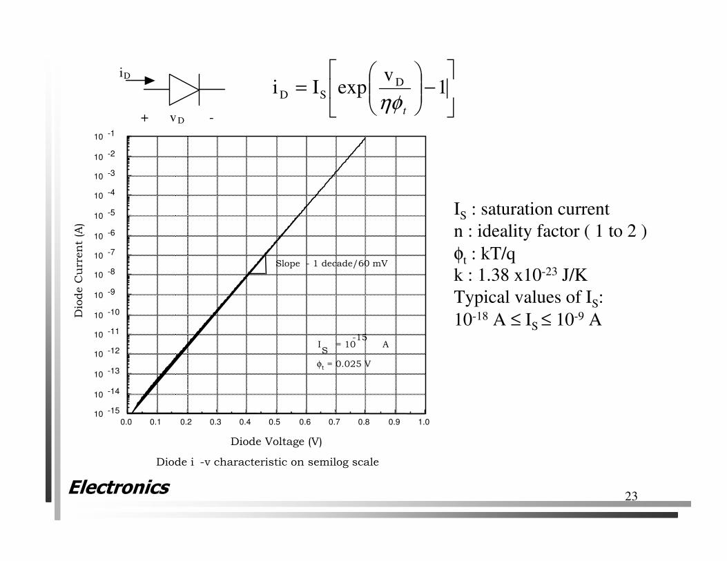
Diode Voltage (V)
1.00.90.80.70.60.50.40.30.20.10.010 -15
10 -14
10 -13
10 -12
10 -11
10 -10
10 -9
10 -8
10 -7
10 -6
10 -5
10 -4
10 -3
10 -2
10 -1
Diode Current (A)
φt = 0.025 V
Slope - 1 decade/60 mV
I = 10 AS
-15
Diode i -v characteristic on semilog scale
IS : saturation current
n : ideality factor ( 1 to 2 )
φt : kT/q
k : 1.38 x10⁻²³ J/K
Typical values of IS:
10-18 A ≤ IS ≤ 10-9 A
−
= 1
vexpIi D
SD
tηφ
+ vD -
iD
Electronics24
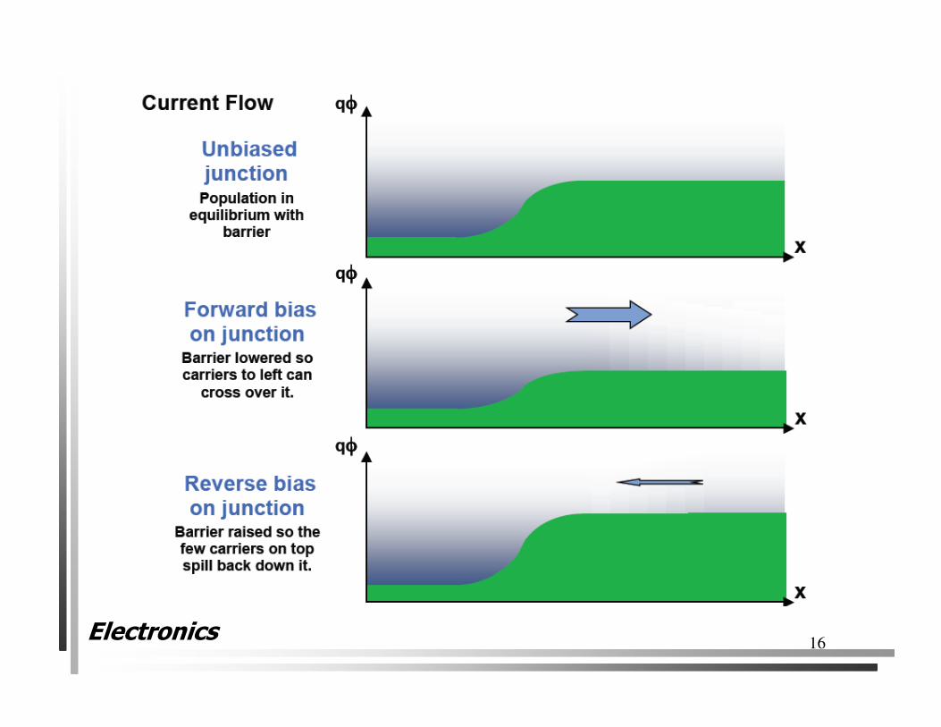
Deviations from the Ideal Diode *
Reverse-biased deviations from ideal
Forward-biased deviations from the ideal
∗ G.W. Neudeck, The PN Junction Diode,
2nd edition, Prentice Hall, 1989
Electronics25
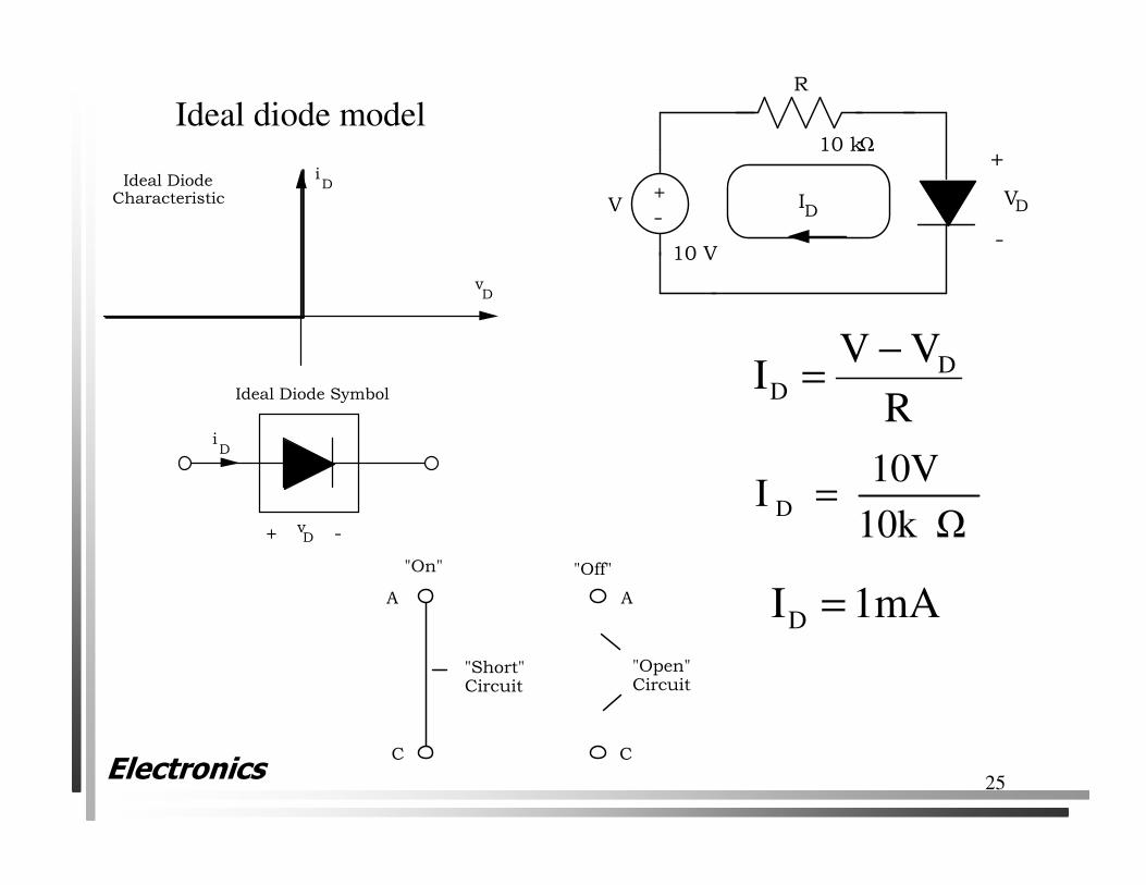
vD
iDIdeal Diode
Characteristic
Ideal Diode Symbol
iD
vD+ -
A
C
"On"
C
A
"Off"
"Short" Circuit
"Open" Circuit
+
-V
10 kΩ
VDID
+
-10 V
R
R
VVI D
D
−=
10k Ω
10VI D =
1mAID =
Ideal diode model
Electronics26
iD
iD
(a) (b)
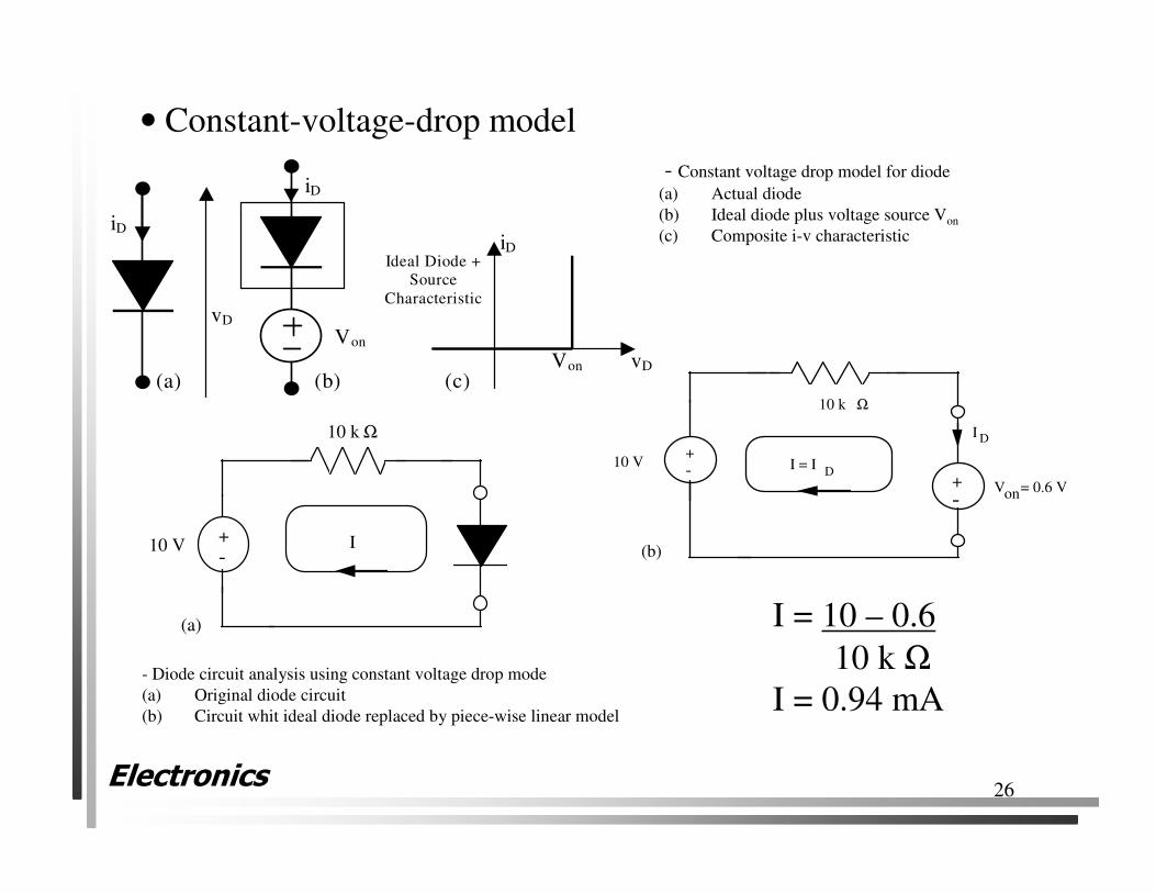
vD Von
Von vD
iD Ideal Diode +
Source
Characteristic
(c)
- Constant voltage drop model for diode
(a) Actual diode
(b) Ideal diode plus voltage source Von
(c) Composite i-v characteristic
+
-10 V
10 k Ω
I
(a)
+
-10 V
10 k Ω
I D
-
(c)
V = 0.6 Von
I = ID
+
(b)
- Diode circuit analysis using constant voltage drop mode
(a) Original diode circuit
(b) Circuit whit ideal diode replaced by piece-wise linear model
I = 10 – 0.6
10 k Ω
I = 0.94 mA
• Constant-voltage-drop model
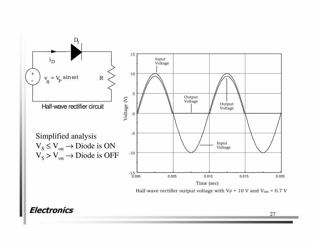
Electronics27
+
- R
iD
D1
v = VPsin ω t
S
Half-wave rectifier circuit
0.0200.0150.0100.0050.000-15
-10
-5
0
5
10
15
Time (sec)
Voltage (V)
InputVoltage
OutputVoltage
InputVoltage
OutputVoltage
Half Half-wave rectifier output voltage with VP = 10 V and Von = 0.7 V
Simplified analysis
VS ≤ Von → Diode is ON
VS > Von → Diode is OFF
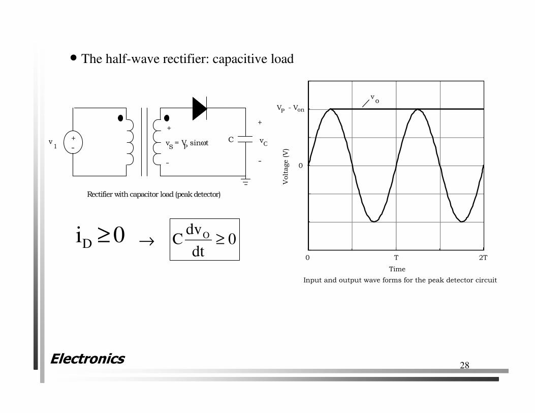
Electronics28
vO
+
-
+
-
v = VPsin ωt
SC+
-v1
Rectifier with capacitor load (peak detector)
Time
Voltage (V)
V - VP on
0 T 2T
0
vo
Input and output wave forms for the peak detector circuit
0iD ≥ 0dt
dvC O ≥
• The half-wave rectifier: capacitive load
→
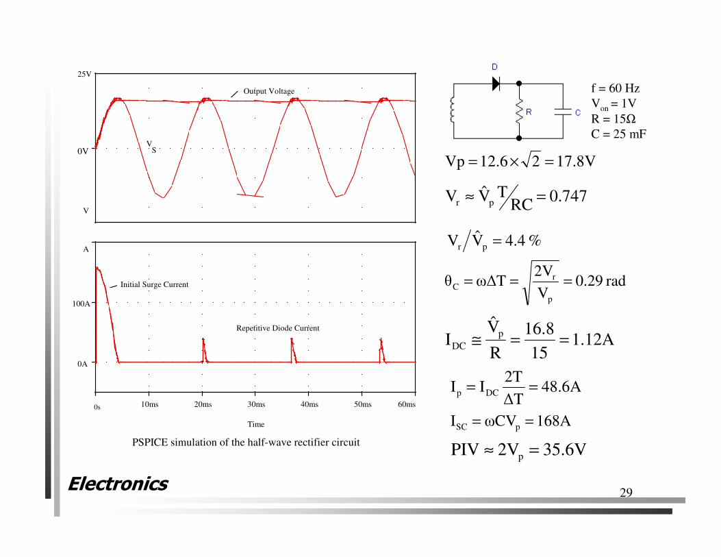
Electronics29
0s 10ms 20ms 30ms 40ms 50ms 60ms
Time
Initial Surge Current
Repetitive Diode Current
0V
Output Voltage
VS
0s
0A
100A
A
V
0V
25V
PSPICE simulation of the half-wave rectifier circuit
17.8V212.6Vp =×=
0.747RC
TVV pr =≈
% 4.4VV pr =
rad 0.29V
2Vω∆Tθ
p
rC ===
f = 60 Hz
Von = 1V
R = 15Ω
C = 25 mF
1.12A15
16.8
R
VI
p
DC ==≅
48.6A∆T
2TII DCp ==
168AωCVI pSC ==
35.6V2VPIV p =≈
Electronics30
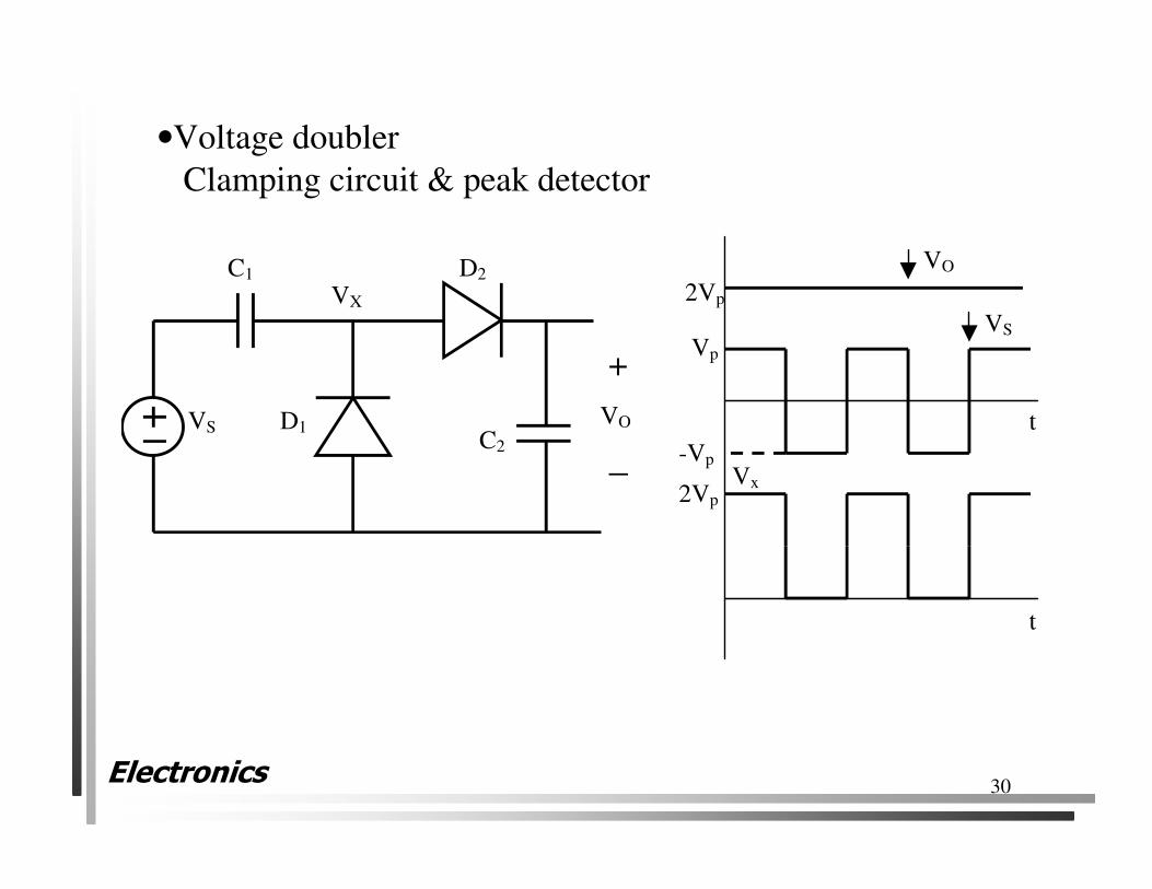
VS D1
D2 VX
C1
C2
+
_
VO
•Voltage doubler
Clamping circuit & peak detector
2Vp
Vp
-Vp
2Vp
VO
VS
t
t
Vx
Electronics31
References
– EEL 7061 Eletrônica Básicahttp://www.eel.ufsc.br/electronics/index7061.htm
– Reid R. Harrison, “Analog Integrated Circuit Design”ECE/CS 5720/6720 Department of Electrical and Computer Engineering University of Utah
– Charles Sodini, “6.012 Microelectronic Devices and Circuits”,OpenCourseWarehttp://ocw.mit.edu