Advancing nanoelectronic device modeling through peta ...
16
Advancing nanoelectronic device modeling through peta-scale computing and deployment on nanoHUB Benjamin P. Haley 1,2 , Sunhee Lee 2 , Mathieu Luisier 1,2 , Hoon Ryu 2 , Faisal Saied 3,4 , Steve Clark 3 , Hansang Bae 2 and Gerhard Klimeck 1,2 1. Network for Computational Nanotechnology, Purdue University 2. School of Electrical and Computer Engineering, Purdue University 3. Rosen Center for Advanced Computing, Purdue University 4. Computing Research Institute, Purdue University [email protected] Abstract. Recent improvements to existing HPC codes NEMO 3-D and OMEN, combined with access to peta-scale computing resources, have enabled realistic device engineering simulations that were previously infeasible. NEMO 3-D can now simulate 1 billion atom systems, and, using 3D spatial decomposition, scale to 32768 cores. Simulation time for the band structure of an experimental P doped Si quantum computing device fell from 40 minutes to 1 minute. OMEN can perform fully quantum mechanical transport calculations for real- word UTB FETs on 147,456 cores in roughly 5 minutes. Both of these tools power simulation engines on the nanoHUB, giving the community access to previously unavailable research capabilities. 1. Introduction The rapid progress in nanofabrication technologies has led to the emergence of new classes of nano- devices, in which the quantum nature of charge carriers dominates the device properties and performance. The need for atomistic-level modeling is particularly clear in studies of quantum dots. Quantum dots are solid-state structures capable of trapping charge carriers so that their wave functions become fully spatially localized, and their energy spectra consist of well-separated, discrete levels. Existing nanofabrication techniques make it possible to manufacture quantum dots in a variety of types and sizes [1]. Among them, semiconductor quantum dots grown by self-assembly (SADs), trapping electrons as well as holes, are of particular importance in quantum optics, since they can be used as detectors of infrared radiation [2], optical memories [3], and single photon sources [4]. Arrays of quantum-mechanically coupled SADs can also be used as optically active regions in high- efficiency, room-temperature lasers [5]. Atomic scale modeling is also critical for studying concepts such as silicon-on-insulator ultra-thin- body (UTB) devices [6], multi-gate nanowires [7-8], and band-to-band tunneling field-effect transistors (TFETs) [9-10]. In these regimes, classical simulation approaches, such as the drift- diffusion [11] and effective mass [12] models, do not correctly capture the strong quantization effects, which influence device performance. The goal of this paper is to present new capabilities that have been added to our Nanoelectronic Modeling tool set. We are in the process of developing, in OMEN, a single code that will include the
Transcript of Advancing nanoelectronic device modeling through peta ...
Advancing nanoelectronic device modeling through peta-scale computing and deployment on nanoHUB
Benjamin P. Haley1,2, Sunhee Lee2, Mathieu Luisier1,2, Hoon Ryu2, Faisal Saied3,4, Steve Clark3, Hansang Bae2 and Gerhard Klimeck1,2
1. Network for Computational Nanotechnology, Purdue University 2. School of Electrical and Computer Engineering, Purdue University 3. Rosen Center for Advanced Computing, Purdue University 4. Computing Research Institute, Purdue University
Abstract. Recent improvements to existing HPC codes NEMO 3-D and OMEN, combined with access to peta-scale computing resources, have enabled realistic device engineering simulations that were previously infeasible. NEMO 3-D can now simulate 1 billion atom systems, and, using 3D spatial decomposition, scale to 32768 cores. Simulation time for the band structure of an experimental P doped Si quantum computing device fell from 40 minutes to 1 minute. OMEN can perform fully quantum mechanical transport calculations for real-word UTB FETs on 147,456 cores in roughly 5 minutes. Both of these tools power simulation engines on the nanoHUB, giving the community access to previously unavailable research capabilities.
1. Introduction The rapid progress in nanofabrication technologies has led to the emergence of new classes of nano-devices, in which the quantum nature of charge carriers dominates the device properties and performance. The need for atomistic-level modeling is particularly clear in studies of quantum dots. Quantum dots are solid-state structures capable of trapping charge carriers so that their wave functions become fully spatially localized, and their energy spectra consist of well-separated, discrete levels. Existing nanofabrication techniques make it possible to manufacture quantum dots in a variety of types and sizes [1]. Among them, semiconductor quantum dots grown by self-assembly (SADs), trapping electrons as well as holes, are of particular importance in quantum optics, since they can be used as detectors of infrared radiation [2], optical memories [3], and single photon sources [4]. Arrays of quantum-mechanically coupled SADs can also be used as optically active regions in high-efficiency, room-temperature lasers [5].
Atomic scale modeling is also critical for studying concepts such as silicon-on-insulator ultra-thin-body (UTB) devices [6], multi-gate nanowires [7-8], and band-to-band tunneling field-effect transistors (TFETs) [9-10]. In these regimes, classical simulation approaches, such as the drift-diffusion [11] and effective mass [12] models, do not correctly capture the strong quantization effects, which influence device performance.
The goal of this paper is to present new capabilities that have been added to our Nanoelectronic Modeling tool set. We are in the process of developing, in OMEN, a single code that will include the
functionality of the well-established NEMO 3-D code for strain and electronic structure computations as well as a new capability to solve the challenging 3D quantum transport problem. OMEN is designed to run efficiently on large NSF Track 2 systems like Ranger, at TACC, and Kraken, at NICS. We believe that OMEN will be one of the premier simulation tools for the design and analysis of realistic nanoelectronic devices, and, therefore, it will be an extremely useful tool for the Network for Computational Nanotechnology (NCN) community.
The recent advances in OMEN and NEMO 3-D include algorithmic refinements, performance analysis to identify the best computational strategies, and porting to state of the art HPC architectures, including Ranger, the BlueGene, and Cray XT5, as well as a Woodcrest Linux cluster. One important consequence of these enhancements is the ability to run 3D quantum transport computations. Performing such calculations for realistic devices is a very challenging computational problem, and it represents a new capability for which resources of the scale of Ranger and Kraken are essential. We present initial results for the transport problem on both machines. We also present results for the electronic structure computations based on both the NEMO 3-D code, and the new implementation in OMEN. From an algorithmic point of view, a key challenge for electronic structure is the extraction of interior, degenerate eigenvectors at this scale. These calculations have been carried out on up to 8K cores on the BlueGene and the Cray XT3, and for 32K cores, and 1 billion atoms, on Kraken (XT5).
The rest of the paper is structured as follows. In section 2 we review the physical models underlying NEMO 1-D, NEMO3-D, and OMEN and highlight some of they insights gained from these models; in section 3, we describe the approach used for the parallelization of the computations. In section 4, we briefly describe the algorithms implemented in the packages. Section 5 has the performance results, including benchmark results for 3D transport up to 65K cores, and up to 32K cores in the electronic structure phase. Section 6 describes the deployment of these codes on the nanoHUB.
2. Physical models Figure 1 shows the evolution from the NEMO 1-D and NEMO 3-D codes to OMEN. NEMO 1-D is a mature code that computes quantum transport for a 1D system such as the resonant tunneling diode shown in Fig. 1a. A critical modeling capability is the ability to model an open quantum mechanical system where carriers are injected on one side of the device and extracted at the other side. This constitutes a quantum statistical mechanics problem in non-equilibrium. The non-equilibrium Green function formalism (NEGF) is well established [53, 54] to solve this problem where a Hermitian system Hamiltonian is augmented by open boundary conditions, creating a non-Hermitian system. A set of Green functions is needed to compute the states in the system as well as the occupancy and availability of states and the transfer of carriers from one state to the next. For an overview of the NEGF formalism we refer the reader to a web-page on nanoHUB.org which is authored and maintained by Prof. Supriyo Datta.
There were three key insights in the modeling of resonant tunneling diodes. One was the need to model extended devices through novel boundary conditions [55] which includes quantum charge self-consistency and strong ineleastic scattering or quasi equilibrium in the contacts. The second key insight is that inelastic scattering from acoustic and polar optical phonons, alloy disorder, and interface roughness in the central device region can be modeled quantitatively in NEGF [56-59] and compare well to the valley currents in experimental data at low temperatures. At room temperature, however, a very different physics explains the typical high performance, high current density resonant tunneling diode valley current: It is thermionic emission through excited states. That was the third critical insight that was enabled by the atomistic, layer by layer modeling through empirical tight binding [60,61]. The room temperature calculations require the solution of a double integral in transverse momentum k and total energy E over strongly spiked transmission coefficients (Fig 1b) to result in the overlap of theory with experimental current voltage curves (Fig 1c). Since each bias point is in principle decoupled from the others one can expose a natural multilevel parallelism in voltage, momentum and energy (Fig 1d) [47].

NEMO 3-D can compute strain and electronic structure (but not transport) for 3D devices where the devices are represented atom-by-atom (Fig 1e) [62-64]. The main NEMO 3-D calculation is the strain minimization [62, 16] in a valence force field method and the computation of electronic structure eigenstates, such as that one of an artificial atom / quantum dot depicted in Figure 1f. From these eigenstates one can devise a plethora of properties such as absorption coefficients as symbolized in Fig 1g [67], single impurity characteristics in FinFETs [68], disordered Si quantum wells on SiGe [69], even some general transport characteristics of core-shell nanowires [70] and alloyed nanowires [71]. The first multi-million atom calculations of alloy-disordered systems were demonstrated in 2002 [62,65]. NEMO 3-D is using a 1D layer decomposition as a nearest neighbor CPU communication pattern and was demonstrated to scale well on even the earliest Beowulf cluster computers [62,66]. Later we demonstrated scaling on thin and long nanowire like structures up to 8,192 cores [72]. The NEMO 3-D section below highlights our effort to parallelize NEMO 3-D on more than a single level through 3-D decomposition and parameter sweeps.
Our new OMEN embraces the quantum transport concepts of NEMO 1-D and the 3-D spatial representation of NEMO 3-D. Three dimensional atom arrangements of nanowires realistically gated with dielectrics (Fig 1i) are computed to obtain energy resolved current (Fig 1j) and current voltage characteristics (Fig. 1k). The dramatic work-load increase makes it a perfect candidate for the use of peta-scale computing systems with 4 levels of natural parallelism (Fig. 1l). The code has already been used to model ultra-scaled InAs High-Electron-Mobility Field Effect Transistors (HEMTs) [73], band-to-band tunneling transistors with 2D and 3D device configurations [74], and graphene transistors [75]. An overview of the evolution of NEMO 1-D and NEMO 3-D to OMEN is also presented in reference [76]. Computational results for these capabilities, including scaling to to over 147,000 processors, are presented in section 5.
Figure 1. The NEMO 1-D code can do 1D NEGF quantum transport, while the NEMO 3-D is designed to do strain and electronic calculations. Our new code OMEN incorporates NEMO 3-D functionality and adds a 3D quantum transport capability, and includes features that make the code peta-scale capable.

2.1. NEMO 3D We summarize here some of the key features of the model and the NEMO 3-D package, which consists of three main parts:
• The geometry constructor (setup phase) • The strain computation • The electronic structure computation
Geometry constructor and setup. The geometry constructor’s purpose is to represent the nanostructure in atomistic detail in the memory of the computer. Each atom is represented by its coordinates, its type (atomic number), whether the atom is on the surface or in the interior of the sample (important later on in electronic calculations), in what kind of computation it will participate (strain only or strain and electronic), and its nearest neighbors. This part of NEMO 3-D consumes only a small fraction of total computational time and memory, and will not be discussed further.
The strain computation. The materials making up a quantum dot nanostructure differ in their lattice constants. This lattice mismatch leads to strain; atoms throughout the sample are displaced from their bulk positions. Knowledge of equilibrium atomic positions is crucial for the subsequent calculation of the quantum dot’s electronic properties, which makes the computation of strain a necessary step in realistic simulations of these nanostructures. NEMO 3-D computes strain using an atomistic valence force field method (VFF) [16]. In this approach, the total elastic energy of the sample is computed as a sum of bond-stretching and bond-bending contributions from each atom. The equilibrium atomic positions are found by minimizing the total elastic energy of the system.
The electronic structure computation. The single-particle energies and wave functions are calculated using an empirical first-nearest-neighbor tight-binding model. The underlying idea of this approach is the selection of a basis consisting of atomic orbitals (such as s, p, d, and s*) centered on each atom. These orbitals are treated as a basis set for the Hamiltonian operator and lead to a discrete Hamiltonian matrix that has a block tri-diagonal structure due to the restriction to nearest neighbor interactions. The parameterization of bonds using analytical forms of directional cosines is given in Ref. [17]. NEMO 3-D uses the parameterization for the sp3d5s* model, in which each atom is assigned 20 spin-degenerate orbitals [18].
The 20-band nearest-neighbor tight-binding model is parameterized by 34 energy constants, which need to be established by fitting the computed electronic properties of materials to those measured experimentally. This is done by considering bulk semiconductor crystals (such as GaAs or InAs) under strain. A genetic algorithm is used to search for optimal parameters, described in detail in Refs. [18-20]. Once a parameterization it is known for each material constituting the quantum dot, a full atomistic calculation of the single-particle energy spectrum is carried out on samples composed of millions of atoms. Calculating the electronic structure is the most computationally intensive phase of the code. The eigenvalue problem is solved in parallel using one of the algorithms discussed in Section 4.
2.2. OMEN OMEN is a one-, two-, and three-dimensional quantum transport simulator based on the nearest-neighbor tight-binding method and dedicated to next generation transistors like ultra-thin body (UTB), nanowire, and band-to-band tunneling field-effect transistors. It contains four levels of parallelism, and has already demonstrated scaling up to 65,536 cores with a performance of 208 TFlop/s [21].
OMEN solves the Schrödinger equation with open boundary conditions in an orbital basis. The computational burden directly depends on the complexity of this basis. As one uses more orbitals to describe an atom (from 1 to 20), the size of the Hamiltonian matrices increase, as does the work required to solve the Schrödinger equation. As an alternative to the popular Non-Equilibrium Green’s Function (NEGF) formalism, OMEN uses a Wave Function (WF) approach that is physically identical to NEGF, but computationally less expensive for ballistic transport [15]. In the WF formalism the Schrödinger equation takes the form of a sparse linear system of equations “Ax=b” with a block tri-diagonal matrix “A” of size N =NA × tb, equal to the number of atoms in the structure (NA) times the

number of orbitals of the tight-binding model (tb ). For example, tb =10 in the sp3d5s model without spin-orbit coupling. The first and the last diagonal blocks of the matrix A contain the open-boundary conditions, the multiple right-hand-side vector “b” the injection mechanism. Typical device structures are composed of 10,000 to 200,000 atoms, resulting in matrices of size 50,000< N <1,000,000, depending on the value of tb.
The resulting charge and current densities are then self-consistently coupled to the Poisson equation expressed in a finite-element basis. Hence, ballistic transport, source-to-drain tunneling, alloy disorder, strain, and interface roughness can be treated on an atomistic level in n- or p-doped FETs with a cross section up to about 22 nm2 for circular or square nanowire and a width of 8 nm for UTB. Transistor structures made of several semiconductor materials, such as Si, Ge, SiGe, GaAs, or InAs and with any channel orientation (<100>, <110>, <111>, or <112>) can be investigated. As an example a double-gate UTB FET with transport along the <100> axis is considered in Figure 2 [13-15].
Figure 2. Schematic view of a double-gate ultra-thin body field effect transistor with transport along the <100> crystal axis and confinement along <010>.
3. Parallelization
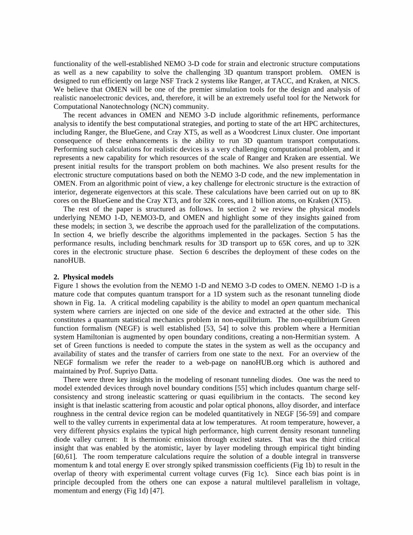
3.1. NEMO 3-D To extend NEMO 3-D performance, the new features of NEMO 3-D include 3D domain decomposition parallelism (Figure 3). Recent benchmarks show that 3D domain decomposition scheme can be utilized exceeding 32,000 cores on realistic electronic structures comprised of one billion atoms. The spatial decomposition can be placed in the lowest level of parallelization for solving eigenstates and charge of general electronic structures.
Additionally, NEMO 3-D is prepared with programmable multiple-level parallelization (Figure 3) which is similar to the tri-level parallelism in NEMO 1-D (bias-energy-momentum) [22] and four-level parallelism in OMEN (bias-energy-momentum-1D spatial decomposition) [23-24]. However the parallelization scheme is different in a sense that the variables involved in each level can determined depending on the application. For example, if we are interested in self-consistent band structure of a highly doped wire with respect to temperature and magnetic field of 20 and 10 samples, respectively, the branch immediately spreads out into 200 independent tasks. With the addition of 10 momentum groups and 50 processors for spatial decomposition, then 100,000 cores can be immediately employed for simulation with nearly ideal scalability.
3.2. OMEN Quantum transport calculations involve solving many linear system of equations (LSE); when hundred of thousands of LSEs have to be solved to simulate the properties of a given device, the solution time becomes an issue. In effect a LSE “Ax=b” must be treated for each energy (typically 500 to 10,000) and momentum (1 to 50) used to inject states into the simulation domain and for each applied voltage (15 to 100 drain-to-source and gate-to-source bias combinations). In the most advantageous case this represents 7,500 LSE, but 50 million in the worst case.
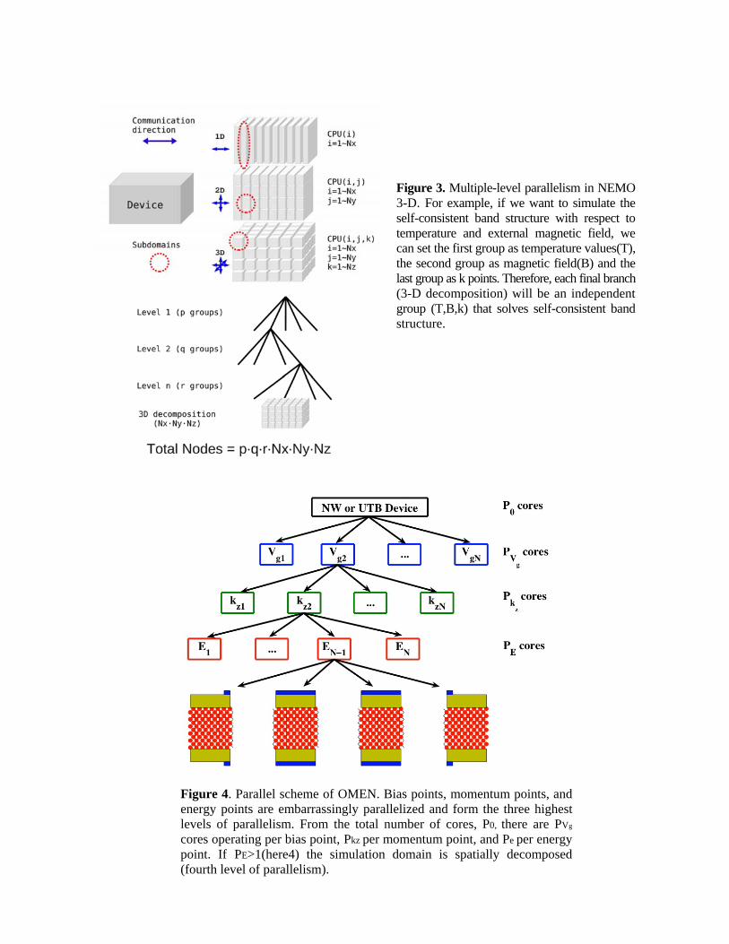
Figure 3. Multiple-level parallelism in NEMO 3-D. For example, if we want to simulate the self-consistent band structure with respect to temperature and external magnetic field, we can set the first group as temperature values(T), the second group as magnetic field(B) and the last group as k points. Therefore, each final branch (3-D decomposition) will be an independent group (T,B,k) that solves self-consistent band structure.
Figure 4. Parallel scheme of OMEN. Bias points, momentum points, and energy points are embarrassingly parallelized and form the three highest levels of parallelism. From the total number of cores, P0, there are PVg cores operating per bias point, Pkz per momentum point, and Pe per energy point. If PE>1(here4) the simulation domain is spatially decomposed (fourth level of parallelism).
To accelerate the computation of all the LSE three natural levels of parallelism have been identified in OMEN: energy, momentum, and bias points. The two first levels (energy and momentum) are almost embarrassingly parallel, they just call the function “MPI Allreduce” at the end of the calculation to sum over the contributions from all the processors. The bias points are completely independent. These three levels are controlled by MPI instructions. The parallelization scheme of OMEN is shown in Figure 4.
The distribution of cores to each task is decided by the user at the beginning of the simulation. This works fine with the bias and the momentum points since their respective number is known at the beginning of the simulation. However, the number of energy points is different for each momentum, not known at the beginning of the simulation, and requires an automatic redistribution of the number of cores per momentum point to equalize the work load as much as possible [21].
The fourth level of parallelism in OMEN, labeled “spatial domain decomposition”, is directly related to the calculation of the open boundary conditions (OBCs), the construction of the matrix “A” and of the vector “b”, and the solution of the sparse linear system of equations “Ax=b”. The open boundary conditions are parallelized by treating each open contact on a different CPU. Since most of the time a device has only two open contacts the calculation of the OBCs does not scale beyond two cores.
4. Algorithms
4.1. NEMO 3-D To find the energy levels and wave functions of the electronic structure, in a quantum dot, for example, we need to solve a large eigenvalue problem arising from the discretization of the time-independent Schrödinger equation iii EH ψψ
rr= , where H is the n by n Hamiltonian matrix, iψ
r is the
eigenvector representing the wave function associated with the eigenvalue iE representing the i-th energy level. We have implemented the Lanczos algorithm [25] in NEMO 3-D and in OMEN. For a standard symmetric eigenvalue problem, this algorithm builds an orthonormal basis kV for a Krylov subspace associated with the Hamiltonian, and a k by k tridiagonal matrix kT such that the following
relationship (the Lanczos factorization) is satisfied: Tkkkkkkk evtTVHV rr
,1++=
It has been shown [26] that the eigenvalues of kT tend to eigenvalues of H as k tends to n. Moreover, some eigenvalues of kT converge to eigenvalues of H very quickly. The problem of finding eigenvalues iE of H is then reduced to the much easier problem of finding eigenvalues of a small tridiagonal matrix kT and the eigenvectors iψ
r of H are found to be kkk WV=][ 1 ψψ
rK
r , where
kW are the eigenvectors of kT . The advantage of Lanczos algorithm is that it is fast. However, it cannot compute repeated eigenvalues. This is addressed by our implementation of block Lanczos, which we do not discuss here. We have also implemented Trace Minimization [27-28] and Rayleigh-Ritz eigenvalue solvers, and interfaced the PARPACK library [29] to NEMO 3-D.
4.2. OMEN The LSE “Ax=b” are solved in parallel using direct sparse linear solver libraries like MUMPS [30], SuperLUdist [31], Pardiso [32], or a customized block cyclic reduction (BCR) of the matrix “A” [33]. Some of the algorithms work with MPI in a distributed memory way (MUMPS, SuperLUdist , BCR), others (Pardiso, BCR again) with OpenMP on shared memory machines. In 3D nanowire structures the BCR outperforms the other solvers by a factor of 2 if spin-orbit coupling is not included [34]. Another advantage of the BCR algorithm is that it allows an interleaved calculation of the open boundary conditions and of the solution of “Ax=b”. Standard packages like MUMPS, SuperLUdis , or Pardiso need the completely assembled matrix “A” at the beginning of the factorization phase. The
BCR algorithm can start working on a matrix “A” not including its first and last diagonal blocks since they are only used at the last step of the reduction of “A”. Consequently, the calculation of the OBCs can scale beyond 2 cores and better computational performance is obtained compared to a sequential approach [21].
Once all the LSE are solved the carrier density and the electrostatic potential in the device are calculated from the wave function coefficients stored in the vector “x” of “Ax=b”. The solution of Schrödinger equation is self-consistently coupled to the Poisson equation described on a three-dimensional finite element mesh [35-36]. To reduce the computational burden Poisson equation is solved in parallel up to 512 cores using Aztec [37], an iterative sparse linear solver. On multi-core supercomputers OMEN has the ability to work either with four levels of MPI parallelization as described above or with 2.5 levels of MPI parallelization (bias, momentum, and energy points across the nodes) and 1.5 levels of OpenMP parallelization (energies within one node and spatial domain decomposition) [21]. The hybrid OMEN requires nested parallelization [38] which is not possible on all the machines due to compiler issues. The MPI-OpenMP hybrid version of OMEN was tested up to 60,000 cores on Ranger at TACC, scaled almost perfectly there, and helped reduce the start up time of the simulations.
5. Results
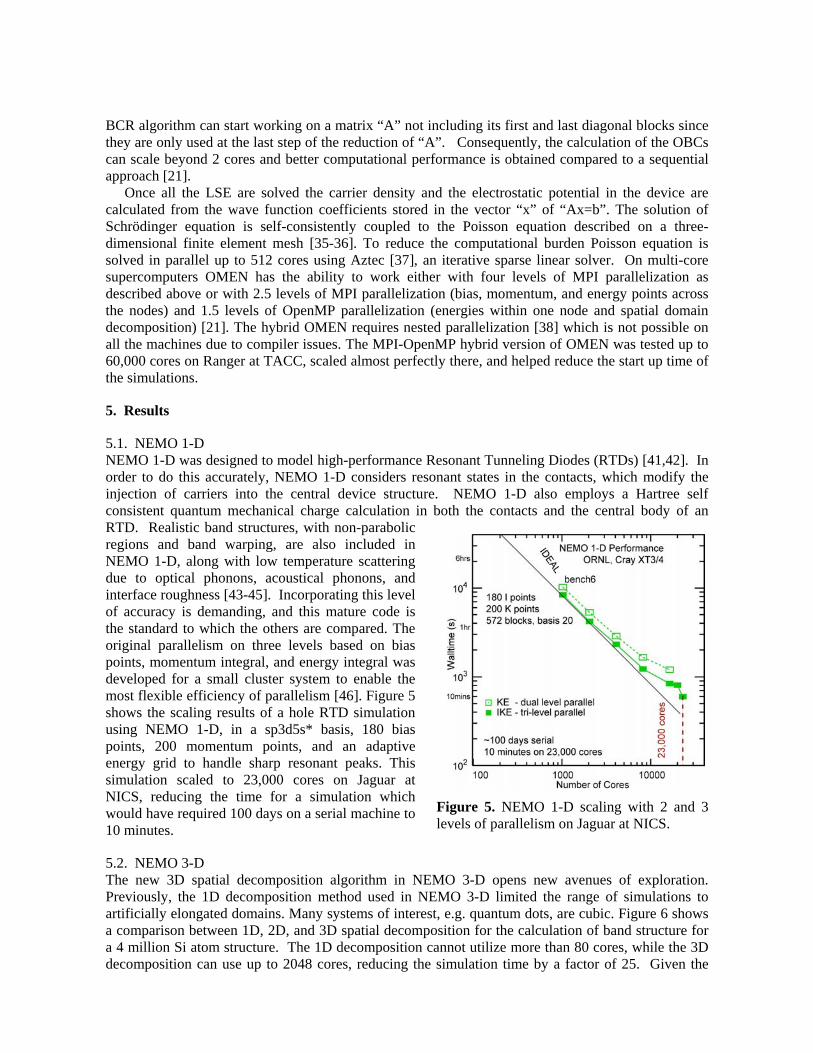
5.1. NEMO 1-D NEMO 1-D was designed to model high-performance Resonant Tunneling Diodes (RTDs) [41,42]. In order to do this accurately, NEMO 1-D considers resonant states in the contacts, which modify the injection of carriers into the central device structure. NEMO 1-D also employs a Hartree self consistent quantum mechanical charge calculation in both the contacts and the central body of an RTD. Realistic band structures, with non-parabolic regions and band warping, are also included in NEMO 1-D, along with low temperature scattering due to optical phonons, acoustical phonons, and interface roughness [43-45]. Incorporating this level of accuracy is demanding, and this mature code is the standard to which the others are compared. The original parallelism on three levels based on bias points, momentum integral, and energy integral was developed for a small cluster system to enable the most flexible efficiency of parallelism [46]. Figure 5 shows the scaling results of a hole RTD simulation using NEMO 1-D, in a sp3d5s* basis, 180 bias points, 200 momentum points, and an adaptive energy grid to handle sharp resonant peaks. This simulation scaled to 23,000 cores on Jaguar at NICS, reducing the time for a simulation which would have required 100 days on a serial machine to 10 minutes.
5.2. NEMO 3-D The new 3D spatial decomposition algorithm in NEMO 3-D opens new avenues of exploration. Previously, the 1D decomposition method used in NEMO 3-D limited the range of simulations to artificially elongated domains. Many systems of interest, e.g. quantum dots, are cubic. Figure 6 shows a comparison between 1D, 2D, and 3D spatial decomposition for the calculation of band structure for a 4 million Si atom structure. The 1D decomposition cannot utilize more than 80 cores, while the 3D decomposition can use up to 2048 cores, reducing the simulation time by a factor of 25. Given the
Figure 5. NEMO 1-D scaling with 2 and 3 levels of parallelism on Jaguar at NICS.

availability of HPC resources, this capability brings previously unrealistic simulations into the realm of practical consideration.
The 3D spatial decomposition also enables much larger simulations. Figure 7 shows simulations of cubic structures with up to 1 billion atoms, using up to 32768 cores on Kraken XT5 at NICS. NEMO 3-D can now make very efficient use of HPC resources to perform studies which would otherwise be impossible.
One such system of interest is a thin highly doped phosphorous region in a Si substrate, which is of interest to experimentalists and theoreticians for potential use in quantum computing systems [39-40]. Figure 8 shows the scaling of an end-to-end band structure calculation of a 2D Si-P bar 1.1 x 1.1 x 22 nm3. Spatial decomposition and momentum space parallelism reduce the simulation time for this system from 40 minutes to 1 minute.
5.3. OMEN OMEN has enabled fully quantum transport simulations of realistic devices. For example, Figure 9 shows the scaling for simulations of a 2D Si double gate ultra-thin-body (UTB) transistor, with a thickness of 5 nm, gate length 22 nm, and total length 42 nm. Four levels of parallelism are employed: 16 applied bias points, 16 momentum points, 800 to 1400 energy points, and spatial decomposition on 2 cores. These simulations scaled to 65536 cores on Kraken at NICS and Ranger at TACC. The availability of the peta-scale resources makes the total simulation time for a fully quantum mechanical calculation very manageable.
Very recently we were given access to the Leadership Computing Facility at Oak Ridge with its Cray XT5 Jaguar. On that resource we demonstrated scaling to 147,456 cores. At that level of parallelism the code delivered around 504 TFLOP/s at 37% of peak for each CPU. We note here that no special tuning was performed on this platform to obtain this high peak performance.
6. Deployment on nanoHUB.org nanoHUB.org is a community web site intended to deliver on-line simulation and more to the nanotechnology community at large. Over 150 tools are now on line which have delivered over 400,000 simulations to over 7,000 users in the 12 months leading up to May 2009. All the simulation
Figure 6. Comparison between different domain decomposition algorithms. Tested with 44 x 44 x 44 (nm3) silicon structure that has 4 million atoms. Ranger@TACC computational resources were used.
Figure 7. Strong scaling plots with NEMO 3-D for different number of atoms. Tested on Kraken@NICS (XT5).

tools are fully interactive in that users can easily set-up their numerical experiments and “what if?” questions and compare their simulation results after the computation. No installation of software is needed on the user end, compute cycles, the graphical user interface, tools, and instructional materials are delivered remotely. Tools of various computational intensity are hosted, many of them executing in a few minutes, few of them running in parallel on computational resources like the TeraGrid. Over 430 citations in the literature are evidence of use in peer-reviewed research — 52% of these citations are unaffiliated with the host of the nanoHUB: The Network for Computational Nanotechnology. nanoHUB has also been used in over 290 classes in over 90 different institutions for educational purposes. More information can be found on http://nanoHUB.org/about and http://nanoHUB.org/usage as well as several peer reviewed articles [47-52].
Both NEMO 3-D and OMEN drive computational tools on nanoHUB.org. OMEN is the underlying engine for the tools OMEN Nanowire and Band Structure Lab, while NEMO 3-D powers Quantum Dot Lab. Figure 10 shows the usage statistics for these simulation tools. Together NEMO 3-D and OMEN have driven thousands of simulations on the nanoHUB, providing cutting-edge research capability for a worldwide user base. We plan to replace the backend of several more tools on the nanoHUB with OMEN or components of OMEN; this will greatly simplify maintenance of those tools and consolidate several competing
Figure 8. The performance of the multi-level parallelism. End-to-end band structure calculation is performed on a small periodic structure with 256 k points considered.
Figure 9: Scaling performances of OMEN up to 65,536 cores for a 2-D DG UTB transistor using four levels of parallelism (16 bias points, 16 momentum points, 800 to1400 energy points, spatial decomposition on 2 cores).
Figure 10. Scaling performances of OMEN up to 147,456 cores for a 2-D DG UTB transistor using four levels of parallelism (16 bias points, 24 momentum points, 850 energy points, spatial decomposition on 8 cores).

implementations into one code base. For example, currently several tools implement a Poisson solver using different methods. In many cases, no one maintains the code. By replacing these with the OMEN solver, we reduce the number of Poisson implementations to one, which is a highly optimized current research tool. The number of simulations run in these OMEN and NEMO3D powered tools are tabulated in Table 1 and the global users are depicted in Figure 11.
Table 1. Usage statistics for OMEN- and NEMO 3-D-powered tools on the nanoHUB.
Figure 11. World map of NEMO3D and OMEN-powered tool users.
7. Conclusions We have made substantial enhancements to the codes NEMO 3-D and OMEN. The enhancements allow the codes to make full use of peta-scale computing resources and opened previously inaccessible realms of device engineering studies. NEMO 3-D can handle billion atom systems, scaling to 32768 cores, using three dimensional spatial decomposition. By making use of large scale computing resources, NEMO 3-D can reduce the calculation time for the band structure of a cutting-edge quantum computing device from 40 minutes to 1 minute. OMEN can model fully quantum mechanical transport in realistic UTB FETs on 147,456 cores in about 15 minutes. These compute engines drive tools on the nanoHUB, presenting users with state-of-the-art research capabilities in their web browsers.
References [1] For reviews and references see, e.g., Jacak, L., Hawrylak, P., and Wojs, A, “Quantum dots”,
Springer-Verlag, Berlin, 1998. [2] Aslan, B., Liu, H.C., Korkusinski, M., Cheng, S.-J., and Hawrylak, P., Appl. Phys. Lett., 82,

630, 2003. [3] Petroff, P.M., in “Single Quantum Dots: Fundamentals, Applications, and New Concepts”,
Peter Michler, Ed., Springer, Berlin, 2003. [4] Michler, P., et al., Science, 290, 2282, 2000; Moreau, E., et al., Phys. Rev. Lett., 87, 183601,
2001. [5] Arakawa, Y., and Sasaki, H., Appl. Phys. Lett., 40, 939, 1982; Fafard, S., et al., Science, 22,
1350, 1996; Maximov, M.V., et al., J. Appl. Phys., 83, 5561, 1998. [6] B. Doris et al., “Extreme scaling with ultra-thin Si channel MOSFETs”, IEDM Tech. Dig. 2002,
267-270 (2002). [7] Y. Cui, L. J. Lauhon, M. S. Gudiksen, J. Wang, and C. M. Lieber, “Diameter-controlled
synthesis of single-crystal silicon nanowires”, Appl. Phys. Lett. 78, 2214 (2001). [8] S. D. Suk et al., “Investigation of nanowire size dependency on TSNWFET”, IEDM Tech. Dig.
2007, 891-894 (2007). [9] J. Appenzeller, Y.-M. Lin, J. Knoch, and Ph. Avouris, “Band-to-Band Tunneling in Carbon
Nanotube Field-Effect Transistors”, Phys. Rev. Lett. 93, 196805 (2004). [10] W. Y. Choi, B.-G. Park, J. D. Lee, and T.-J. King Liu, “Tunneling Field-Effect Transistors
(TFETs) With Subthreshold Swing (SS) Less Than 60 mV/dec”, IEEE Elec. Dev. Lett. 28, 743-745 (2007).
[11] W. Fichtner, D. J. Rose, and R. E. Bank, “Semiconductor-Device Simulation”, IEEE Trans. on Elec. Dev. 30, 1018-1030 (1983).
[12] J. Wang, E. Polizzi, and M. S. Lundstrom, “A three-dimensional quantum simulation of silicon nanowire transistors with the effective-mass approximation”, J. Appl. Phys. 96, 2192-2203 (2004).
[13] M. Luisier, A. Schenk, and W. Fichtner, "Three-Dimensional Full-Band Simulations of Si Nanowire Transistors", IEDM Tech. Digest 2006, 811 (2006).
[14] M. Luisier, A. Schenk, and W. Fichtner, "Atomistic Treatment of interface roughness in Si nanowire transistors with different channel orientations", Appl. Phys. Lett. 90, 102103 (2007).
[15] M. Luisier, G. Klimeck, A. Schenk, and W. Fichtner, "Atomistic Simulation of Nanowires in the sp3d5s* Tight-Binding Formalism: from Boundary Conditions to Strain Calculations", Phys. Rev. B 74, 205323 (2006).
[16] F. Oyafuso, G. Klimeck, P. von Allmen, T. Boykin, and R. C. Bowen, "Strain Effects in large-scale atomistic quantum dot simulations", Phys. Stat. Sol. (b), Vol. 239, p 71-79 (2003).
[17] J. C. Slater and G. F. Koster, “Simplified LCAO Method for the Periodic Potential Problem”, Phys. Rev. 94, 1498-1524 (1954).
[18] Klimeck, G., Oyafuso, F., Boykin, T.B., Bowen, R.C., and von Allmen, P., "Development of a Nanoelectronic 3-D (NEMO 3-D) Simulator for Multimillion Atom Simulations and Its Application to Alloyed Quantum Dots", Computer Modeling in Engineering and Science, 3, 601, 2002.
[19] G. Klimeck, F. Oyafuso, R. C. Bowen, T. B. Boykin, T. A. Cwik, E. Huang, E. S. Vinyard .3-D atomistic nanoelectronic modeling on high performance clusters: multimillion atom simulations., Superlattices and Microstructures, Vol. 31, Nos 2–4, 2002.
[20] F. Oyafuso, G. Klimeck, R. C. Bowen, T. B. Boykin, and P. von Allmen. "Disorder Induced Broadening in Multimillion Atom Alloyed Quantum Dot Systems", Phys. Stat. Sol. (c), vol 0004, pg 1149-1152 (2003).
[21] M. Luisier and G. Klimeck, “Numerical Strategies towards Peta-Scale Simulations of Nanoelectronics Devices”, submitted to SC09 (2009).
[22] Gerhard Klimeck, “Parallelization of the Nanoelectronic Modeling Tool (NEMO 1-D) on a Beowulf Cluster,” Journal of Computational Electronics, Vol 1, Issue 1-2, 2002
[23] Mathieu Luisier and Gerhard Klimeck, “A multi-level parallel simulation approach to electron transport in nano-scale transistors,” Supercomputing 2008, Austin TX, Nov. 15-21 2008.

Regular paper - 59 accepted papers, 277 submissions (21%) [24] Hansang Bae, Steve Clark, Ben Haley, Hoon Ryu, Gerhard Klimeck, Sunhee Lee, Mathieu
Luisier and Faisal Saied, “A Nano-electronics Simulator for Petascale Computing: From NEMO to OMEN,” TeraGrid 2008, Jun 9-13, 2008, Las Vegas
[25] C. Lanczos, “An Iteration Method for the Solution of the Eigenvalue Problem of Linear Differential and Integral Operators”, Journal of Research of the National Bureau of Standards, Vol. 45, No 4, 1950
[26] R.R. Underwood, “An iterative block Lanczos method for the solution of large sparse symmetric eigenproblems”, Ph.D. Dissertation, Stanford University, Stanford, CA, 1975
[27] A. H. Sameh and J. Wisniewski. A Trace Minimization Algorithm for the Generalized Eigenvalue Problem . SIAM Journal on Numerical Analysis , Vol. 19, No. 6, pp. 1243-1259, 1982.
[28] A. Sameh and Z. Tong, The trace minimization method for the symmetric generalized eigenvalue problem. J. Comput. Appl. Math. 123, 155-175, 2000.
[29] K. Maschhoff and D. Sorensen, “A portable implementation of ARPACK for distributed memory parallel architectures”, Copper Mountain Conference on Iterative Methods, 1996
[30] P. R. Amestoy, I. S. Duff, and J.-Y. L’Excellent, “Multifrontal parallel distributed symmetric and unsymmetric solvers” Comput. Methods in Appl. Mech. Eng. 184, 501 (2000).
[31] X. S. Li and J. W. Demmel “SuperLU DIST: A Scalable Distributed Memory Sparse Direct Solver for Unsymmetric Linear Systems”, ACM Trans. on Math. Software 29, 110 (2003).
[32] O. Schenk and K. Gärtner, “Solving Unsymmetric Sparse Systems of Linear Equations with PARDISO”, Journal of Future Generation Computer Systems 20, 475 (2004).
[33] T. B. Boykin, M. Luisier, and G. Klimeck, “Multi-band transmission calculations for nanowires using an optimized renormalization method”, Phys. Rev. B 77, 165318 (2008)
[34] M. Luisier, A. Schenk, W. Fichtner, T. B. Boykin, and G. Klimeck, “A parallel sparse linear solver for nearest-neighbor tight-binding problems”, Proc. of the 14th international Euro-Par conference on Parallel Processing, 790-800 (2008).
[35] P. M. Gresho and R. L. Sani, “Incompressible Flow and the Finite Element Method: Isothermal Laminar Flow”, John Wiley and Sons, New York (2000).
[36] R. E. Bank, D. J. Rose, and W. Fichtner, “Numerical Methods for Semiconductor Device Simulation”, IEEE Trans. Electron Dev. 30, 1031 (1983).
[37] R. S. Tuminaro, M. Heroux, S. A. Hutchinson, and J. N. Shadid, “Official Aztec User’s Guide: Version 2.1” (1999).
[38] A. Duran, M. Gonzalez, and J. Corbalan, “Automatic thread distribution for nested parallelism in OpenMP”, Proceedings of the 19th annual international conference on Supercomputing, 121-130 (2005).
[39] T. C. Shen, J. Y. Ji, M. A. Zudov, R. R. Du, J. S. Kline, J. R. Tucker, “Ultradense phosphorus delta layers grown into silicon from PH3 molecular precursors,” Appl. Phys. Lett. 80, 9, 2002.
[40] Hoon Ryu, Sunhee Lee and Gerhard Klimeck, “A Study of Temperature-dependent properties of n-type delta-doped Si bandstrucstures in equilibrium,” to appear in IEEE proceedings of the 13th International Workshop on Computational Electronics, Tsinghua University, Beijing, May 27-29 2009.
[41] Gerhard Klimeck, Roger K. Lake, R. Chris Bowen, William R. Frensley and Ted Moise, "Quantum Device Simulation with a Generalized Tunneling Formula", Appl. Phys. Lett., Vol. 67, p.2539 (1995).
[42] R. Chris Bowen, Gerhard Klimeck, Roger Lake, William R. Frensley and Ted Moise, "Quantitative Resonant Tunneling Diode Simulation", J. of Appl. Phys. 81, 3207 (1997).
[43] Gerhard Klimeck, Roger Lake and Daniel K. Blanks,"Role of interface roughness scattering in self-consistent resonant tunneling diode simulation", Phys. Rev. B, Vol. 58, 7279 (1998).
[44] Gerhard Klimeck, Roger Lake and Daniel K. Blanks,"Numerical Approximations to the
Treatment of Interface Roughness Scattering in Resonant Tunneling Diodes", Semicond. Sci. Technology, Vol 13, pg. A165 (1998).
[45] Roger Lake, Gerhard Klimeck and Daniel K. Blanks, "Interface Roughness and Polar Optical Phonon Scattering in InGaAs/AlAs/InAs RTDs", Semicond. Sci. Technology, Vol 13, pg. A163 (1998).
[46] Gerhard Klimeck, "Parallelization of the Nanoelectronic Modeling Tool (NEMO 1-D) on a Beowulf Cluster", Gerhard Klimeck, Journal of Computational Electronics, Vol 1, Issue 1-2, pp 75-79 (2002).
[47] Gerhard Klimeck, Michael McLennan, Sean B. Brophy, George B. Adams III, Mark S. Lundstrom, "nanoHUB.org: Advancing Education and Research in Nanotechnology", IEEE Computers in Engineering and Science (CISE), Vol. 10, pg. 17-23 (2008).
[48] Nancy Wilkins-Diehr, Dennis Gannon, Gerhard Klimeck, Scott Oster, Sudhakar Pamidighantam, “TeraGrid Science Gateways, Virtual Organizations and Their Impact on Science", IEEE Computer, Vol. 41, Issue 11, Nov. 2008, Page(s):32 – 41
[49] Benjamin P. Haley, Gerhard Klimeck, Mathieu Luisier, Dragica Vasileska, Abhijeet Paul, Swaroop Shivarajapura, Diane L. Beaudoin, "Computational nanoelectronics research and education at nanoHUB.org", accepted (June 26) for publication to Journal of Computational Electronics (2009).
[50] Shaikh Ahmed, Gerhard Klimeck, Derrick Kearney, Michael McLennan, and M. P. Anantram, "Quantum Simulations of Dual Gate MOSFET Devices: Building and Deploying Community Nanotechnology Software Tools on nanoHUB.org", Journal of High Speed Electronics and Systems, Vol. 17, No 3, pp. 485-494 (2007).
[51] Gerhard Klimeck and Dragica Vasileska, "ABACUS and AQME: Semiconductor Device and Quantum Mechanics Education on nanoHUB.org", IEEE proceedings of the 13th International Workshop on Computational Electronics, Tsinghua University, Beijing, May 27-29 2009, DOI:10.1109/IWCE.2009.5091083.
[52] Gerhard Klimeck, Michael McLennan, Mark S. Lundstrom, George B. Adams III. "nanoHUB.org - online simulation and more materials for semiconductors and nanoelectronics in education and research", 8th IEEE Conference on Nanotechnology, 2008. NANO '08. Aug. 18-21 2008 Page(s):401-404, DOI:10.1109/NANO.2008.124
[53] S. Datta, “The NEGF Approach to Nano-Device Simulation”, http://nanohub.org/topics/negf [54] S. Datta, “Nanoscale Device Simulation: The Green’s Function Method,” Superlattices and
Microstructures, 28, 253-278 (2000). [55] Gerhard Klimeck, Roger K. Lake, R. Chris Bowen, William R. Frensley and Ted Moise,
"Quantum Device Simulation with a Generalized Tunneling Formula", Appl. Phys. Lett., Vol. 67, p.2539 (1995)
[56] Roger K. Lake, Gerhard Klimeck, R. Chris Bowen, Chenjing L. Fernando, Manhua Leng, Ted Moise and Y. C. Kao, "Interface Roughness and Polar Optical Phonon Scattering And the Valley Current in Resonant Tunneling Devices", Superlattices and Microstructures, Vol. 20, p.279 (1996).
[57] Gerhard Klimeck, Roger Lake, Dan Blanks, Chenjing L. Fernando, R. Chris Bowen, Ted Moise, and Y. C. Kao, “The Effects of Electron Screening Length and Emitter Quasi-Bound States on the Polar-Optical Phonon Scattering in Resonant Tunneling Diodes”, Physica Status Solidi (b), Vol. 204, 408 (1997).
[58] Gerhard Klimeck, Roger Lake and Daniel K. Blanks, "Role of interface roughness scattering in self-consistent resonant tunneling diode simulation", Phys. Rev. B, Vol. 58, 7279 (1998).
[59] Roger Lake, Gerhard Klimeck, R. Chris Bowen and Dejan Jovanovic, “Single and multiband modeling of quantum electron transport through layered semiconductor devices”, J. of Appl. Phys. 81, 7845 (1997)
[60] R. Chris Bowen, Gerhard Klimeck, Roger Lake, William R. Frensley and Ted Moise, “Quantitative Resonant Tunneling Diode Simulation”, J. of Appl. Phys. 81, 3207 (1997).

[61] Gerhard Klimeck, Timothy B. Boykin, R. Chris Bowen, Roger Lake, Dan Blanks, Ted Moise,
Y. C. Kao, and William R. Frensley, “Quantitative Simulation of Strained InP-Based Resonant Tunneling Diodes”, in IEEE Proceedings of the 1997 55th IEEE Device Research Conference Digest, IEEE, NJ, p. 92 (1997).
[62] Gerhard Klimeck, Fabiano Oyafuso, Timothy B. Boykin R. Chris Bowen, and, Paul von Allmen, "Development of a Nanoelectronic 3-D (NEMO 3-D) Simulator for Multimillion Atom Simulations and Its Application to Alloyed Quantum Dots (INVITED)", Computer Modeling in Engineering and Science (CMES) Volume 3, No. 5, pp 601-642 (2002), ISSN: 1526-1492.
[63] Gerhard Klimeck, Shaikh Ahmed, Neerav Kharche, Marek Korkusinski, Muhammad Usman, Marta Prada, and Timothy B. Boykin, "Atomistic Simulation of Realistically Sized Nanodevices Using NEMO 3-D: Part II - Applications", Special Issue on Nanoelectronic Device Modeling in IEEE Transactions on Electron Devices, Vol. 54, Issue 9, pg. 2090 - 2099 (2007).
[64] Gerhard Klimeck, Shaikh Ahmed, Hansang Bae, Neerav Kharche, Steve Clark, Benjamin Haley, Sunhee Lee, Maxim Naumov, Hoon Ryu, Faisal Saied, Marta Prada, Marek Korkusinski, and Timothy B. Boykin, "Atomistic Simulation of Realistically Sized Nanodevices Using NEMO 3-D: Part I - Models and Benchmarks", Special Issue on Nanoelectronic Device Modeling in IEEE Transactions on Electron Devices, Vol. 54, Issue 9, pg. 2079 - 2089 (2007).
[65] Fabiano Oyafuso, Gerhard Klimeck, R. Chris Bowen, and Timothy B. Boykin, "Atomistic Electronic Structure Calculations of Unstrained Alloyed Systems Consisting of a Million Atoms", Journal of Computational electronics, Vol. 1. Issue 3, pp. 317-321 (2002).
[66] Gerhard Klimeck, R. Chris Bowen, and Timothy B. Boykin, "Atomistic simulation of quantum dots including strain and bandstructure and full band simulation of hole transport in 1-D heterostructures", in IEEE proceedings of 7th International Workshop on Computational Electronics (IWCE). Book of Abstract, Glasgow 22-25 May 2000, pp 6-7, (2000)
[67] Muhammad Usman, Hoon Ryu, Insoo Woo, David S. Ebert, and Gerhard Klimeck, "Moving towards nano-TCAD through multi-million atom quantum dot simulations matching experimental data", IEEE Transactions on Nanotechnology, Vol. 8, Issue 3, pg. 330-344 (2009), DOI: 10.1109/TNANO.2008.2011900 (2009).
[68] G.P. Lansbergen, R. Rahman, C.J. Wellard, P.E. Rutten, J. Caro, N. Collaert, S. Biesemans, I. Woo, G. Klimeck, L.C.L. Hollenberg, and S. Rogge, "Gate induced quantum confinement transition of a single dopant atom in a Si FinFET", Nature Physics, Vol. 4, pg. 656 (2008).
[69] Neerav Kharche, Marta Prada, Timothy B. Boykin, and Gerhard Klimeck, "Valley-splitting in strained Silicon quantum wells modeled with 2 degree miscuts, step disorder, and alloy disorder", Applied Phys. Lett. Vol. 90, 092109 (2007).
[70] Gengchiau Liang, Jie Xiang, Neerav Kharche, Gerhard Klimeck, Charles M. Lieber, and Mark Lundstrom, "Performance Analysis of a Ge/Si Core/Shell Nanowire Field Effect Transistor", cond-mat/0611226, Nano letters, Vol. 7, 642-646 (2007).
[71] Timothy B. Boykin, Mathieu Luisier, Andreas Schenk, Neerav Kharche, Gerhard Klimeck, "Atomistic, random-alloy calculations of the electronic structure and transmission characteristics of AlGaAs nanowires", IEEE Transactions on Nanotechnology, Vol. 6, No. 1, 43-7 (2007).
[72] Hansang Bae, Steve Clark , Ben Haley, Ryu Hoon, Gerhard Klimeck, Sunhee Lee, Mathieu Luisier, and Faisal Saied, "A Nano-electronics Simulator for Petascale Computing: From NEMO to OMEN", Proceedings of TeraGrid 2008, June 9-13, 2008, Reno, NV.
[73] Mathieu Luisier, Neophytos Neophytou, Neerav Kharche, and Gerhard Klimeck, "Full-Band and Atomistic Simulation of Realistic 40 nm InAs HEMT", IEEE IEDM, San Francisco, USA, Dec. 15-17, 2008, DOI : 10.1109/IEDM.2008.4796842.
[74] Mathieu Luisier, and Gerhard Klimeck, "Atomistic, Full-Band Design Study of InAs Band-to-
Band Tunneling Field-Effect Transistors", IEEE Electron Device Letters, Vol. 30, pp. 602-604 (2009), DOI: 10.1109/LED.2009.2020442 (2009).
[75] Mathieu Luisier, and Gerhard Klimeck, "Performance analysis of statistical samples of graphene nanoribbon tunneling transistors with line edge roughness", Applied Physics Letters, Vol. 94, 223505 (2009), DOI:10.1063/1.3140505
[76] Gerhard Klimeck and Mathieu Luisier, "From NEMO1D and NEMO3D to OMEN: moving towards atomistic 3-D quantum transport in nano-scale semiconductors", IEEE IEDM, San Francisco, USA, Dec. 15-17, 2008, DOI: 10.1109/IEDM.2008.4796647.