Nanoelectronic Programmable Synapses Based on … XXXX American Chemical Society A...
8
rXXXX American Chemical Society A dx.doi.org/10.1021/nl201040y | Nano Lett. XXXX, XXX, 000–000 LETTER pubs.acs.org/NanoLett Nanoelectronic Programmable Synapses Based on Phase Change Materials for Brain-Inspired Computing Duygu Kuzum,* Rakesh G. D. Jeyasingh, Byoungil Lee, and H.-S. Philip Wong Center for Integrated Systems, Department of Electrical Engineering, Stanford University, Stanford, California 94305, United States b S Supporting Information ABSTRACT: Brain-inspired computing is an emerging field, which aims to extend the capabilities of information technology beyond digital logic. A compact nanoscale device, emulating biological synapses, is needed as the building block for brain-like computational systems. Here, we report a new nanoscale electronic synapse based on technologically mature phase change materials employed in optical data storage and nonvolatile memory applications. We utilize continuous resistance transitions in phase change materials to mimic the analog nature of biological synapses, enabling the implementation of a synaptic learning rule. We demonstrate different forms of spike-timing-dependent plasticity using the same nanoscale synapse with picojoule level energy consumption. KEYWORDS: Brain-inspired computing, nanoelectronics, phase change materials, spike timing dependent plasticity, synapse T he efficiency of today’s information processors has been dominated by complementary metaloxidesemiconductor (CMOS) transistor scaling based on Moore’s law. However, in the nano era CMOS scaling started to face significant barriers in achieving historical performance gains. 1 Besides the physical limits, the conventional computing paradigm based on binary logic and Von Neumann architecture becomes increasingly inefficient as the complexity of computation increases. For some computational problems (such as genetics data from DNA microarrays, image and sensor data from satellites, relationships in social networks, and metabolic pathways in biological networks) the computation time scales exponentially with the input size, 2 making it difficult to perform such tasks with conventional computers. Hence, new computational paradigms and architectures are being explored to extend the capabilities of information technology beyond digital logic. As compared to biological systems, today’s programmable computers are 6 to 9 orders of magnitude less efficient in complex environments. 3 Simulating 5 seconds of brain activity takes 500 s and needs 1.4 MW of power, when state-of-the-art supercomputers (i.e., IBM Blue Gene) are used. 4 The power dissipation in the human central nervous system is on the order of 10 W. The superior features of the brain, lacking in today’ s computational systems, are ultrahigh density, low energy consumption, parallelism, robustness, plasticity, and fault-tolerant operation. The human brain consists of ∼10 11 neurons and an extremely large number of synapses, ∼10 15 , which act as a highly complex interconnection scheme among neurons. 5 Synapses dominate the architecture of the brain and are responsible for massive parallelism, structural plasticity, and robust- ness of the brain. They are also crucial to biological computations that underlie perception and learning. 6 Therefore, a compact nanoelectronic device emulating the functions and plasticity of biological synapses will be the most important building block of brain-inspired computational systems. The anatomical discoveries and physiological studies in the twentieth century have led to the theory that learning could be a consequence of changes in the synaptic strength. The well- known theory based on synaptic plasticity, known as Hebbian learning, 7 suggests that the connection strength between Received: March 28, 2011 Revised: May 10, 2011
-
Upload
truongcong -
Category
Documents
-
view
222 -
download
1
Transcript of Nanoelectronic Programmable Synapses Based on … XXXX American Chemical Society A...
rXXXX American Chemical Society A dx.doi.org/10.1021/nl201040y |Nano Lett. XXXX, XXX, 000–000
LETTER
pubs.acs.org/NanoLett
Nanoelectronic Programmable Synapses Based on Phase ChangeMaterials for Brain-Inspired ComputingDuygu Kuzum,* Rakesh G. D. Jeyasingh, Byoungil Lee, and H.-S. Philip Wong
Center for Integrated Systems, Department of Electrical Engineering, Stanford University, Stanford, California 94305, United States
bS Supporting Information
ABSTRACT:
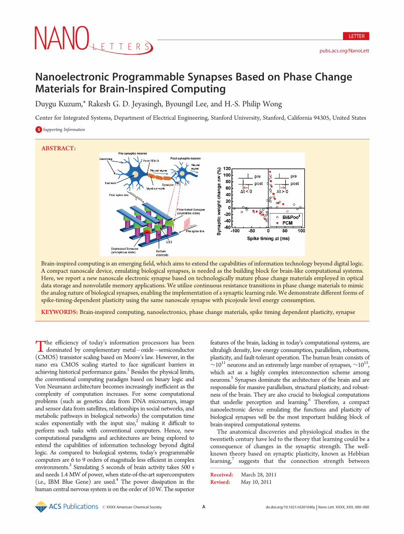
Brain-inspired computing is an emerging field, which aims to extend the capabilities of information technology beyond digital logic.A compact nanoscale device, emulating biological synapses, is needed as the building block for brain-like computational systems.Here, we report a new nanoscale electronic synapse based on technologically mature phase change materials employed in opticaldata storage and nonvolatile memory applications. We utilize continuous resistance transitions in phase change materials to mimicthe analog nature of biological synapses, enabling the implementation of a synaptic learning rule. We demonstrate different forms ofspike-timing-dependent plasticity using the same nanoscale synapse with picojoule level energy consumption.
KEYWORDS: Brain-inspired computing, nanoelectronics, phase change materials, spike timing dependent plasticity, synapse
The efficiency of today’s information processors has beendominated by complementary metal�oxide�semiconductor
(CMOS) transistor scaling based on Moore’s law. However, in thenano era CMOS scaling started to face significant barriers inachieving historical performance gains.1 Besides the physical limits,the conventional computing paradigm based on binary logic andVon Neumann architecture becomes increasingly inefficient as thecomplexity of computation increases. For some computationalproblems (such as genetics data from DNA microarrays, imageand sensor data from satellites, relationships in social networks, andmetabolic pathways in biological networks) the computation timescales exponentially with the input size,2 making it difficult toperform such tasks with conventional computers. Hence, newcomputational paradigms and architectures are being explored toextend the capabilities of information technology beyond digitallogic. As compared to biological systems, today’s programmablecomputers are 6 to 9 orders of magnitude less efficient in complexenvironments.3 Simulating 5 seconds of brain activity takes 500 sand needs 1.4 MW of power, when state-of-the-art supercomputers(i.e., IBM Blue Gene) are used.4 The power dissipation in thehuman central nervous system is on the order of 10W.The superior
features of the brain, lacking in today’s computational systems, areultrahigh density, low energy consumption, parallelism, robustness,plasticity, and fault-tolerant operation. The human brain consists of∼1011 neurons and an extremely large number of synapses,∼1015,which act as a highly complex interconnection scheme amongneurons.5 Synapses dominate the architecture of the brain and areresponsible for massive parallelism, structural plasticity, and robust-ness of the brain. They are also crucial to biological computationsthat underlie perception and learning.6 Therefore, a compactnanoelectronic device emulating the functions and plasticity ofbiological synapses will be the most important building block ofbrain-inspired computational systems.
The anatomical discoveries and physiological studies in thetwentieth century have led to the theory that learning could be aconsequence of changes in the synaptic strength. The well-known theory based on synaptic plasticity, known as Hebbianlearning,7 suggests that the connection strength between
Received: March 28, 2011Revised: May 10, 2011
B dx.doi.org/10.1021/nl201040y |Nano Lett. XXXX, XXX, 000–000
Nano Letters LETTER
neurons is modified based on neural activities in presynaptic andpostsynaptic cells. Spike-timing dependent plasticity (STDP), aform of Hebbian learning, which relies on relative spike timingsof presynaptic and postsynaptic neurons has been discovered inseveral biological systems8�10 in 1990s. STDP as a quantifiable,robust phenomenon providing an intuitive cellular mechanismfor learning has attracted a lot of attention in theoretical studieson the learning rules.11�14
CMOSbased architectures15�17 have been designed to emulatebiological synapses in the past. However, this approach occupies avery large area (at least∼10 transistors per synapse) and, hence itis not practical for designingmassively parallel systemswith 1015 ofthese circuits. Recently, several devices18�20 have been demon-strated that could be potentially used to emulate biological
synapses. In addition to basic synaptic functionality, an electronicanalogue of a biological synapse8�10 needs to exhibit STDPwith acumulative weight change dependent on the number of spike pairsand a maximumweight change of 100%. Such a device should alsohave programming flexibility to capture the variation and thedifferent forms of STDP observed in biological synapses. Ananoscale electronic device with these characteristics that canoperate on the picojoule energy consumption level is yet to bedemonstrated. Motivated by this challenge, we investigate the useof phase change materials as electronic synapses by engineeringtheir switching characteristics. Phase change materials have beenintensively explored for memory applications due to its scalability,fast write/erase speed, and good endurance characteristics21�26
and recently introduced in the marketplace as a commercially
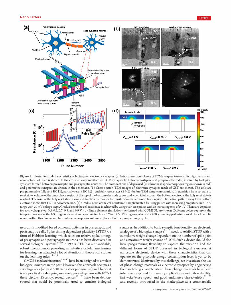
Figure 1. Illustration and characteristics of bioinspired electronic synapses. (a) Interconnection scheme of PCM synapses to reach ultrahigh density andcompactness of brain is shown. In the crossbar array architecture, PCM synapses lie between postspike and prespike electrodes, inspired by biologicalsynapses formed between presynaptic and postsynaptic neurons. The cross sections of depressed (mushroom shaped amorphous region shown in red)and potentiated synapses are shown in the schematic. (b) Cross-section TEM images of electronic synapses made of GST are shown. The cells areprogrammed to fully set (500Ω), partially reset (200 kΩ), and fully reset states (2 MΩ) before TEM sample preparation. In transition from set state toreset state, volume of the amorphous region at the top of the bottom electrode grows and when it fully covers the bottom electrode, the fully reset state isreached. The inset of the fully reset state shows a diffraction pattern for the mushroom shaped amorphous region. Diffraction pattern away from bottomelectrode shows that GST is polycrystalline. (c) Gradual reset of the cell resistance is implemented by using pulses with increasing amplitude in 2�4 Vrange with 20mV voltage steps. Gradual set of the cell resistance is achieved by using stair-case pulses with an increasing step of 0.1 V. There are 20 pulsesfor each voltage step, 0.5, 0.6, 0.7, 0.8, and 0.9 V. (d) Finite element simulations performed with COMSOL are shown. Different colors represent thetemperatures across the GST region for reset voltages ranging from 0.7 to 0.9 V. The regions, where T > 900 K, are mapped using a solid black line. Theregion within this line would turn into an amorphous volume at the end of the programming cycle.
C dx.doi.org/10.1021/nl201040y |Nano Lett. XXXX, XXX, 000–000
Nano Letters LETTER
available product.25�27 In thiswork,we capitalize on advances in thismature memory technology and engineer it for a completelydifferent functionality, namely, implementation of synaptic plasticityfor brain-inspired computing. Different from digital memory appli-cations, here we utilize the continuous transition between resistancelevels of phase change materials in an analog manner to emulatebiological synapses (Figure 1a). We explore the important conceptssuch as implementation of STDP by gradual programming of phasechange devices and modulation of STDP parameters and demon-strate low energy consumption of electronic synapses. Scalability ofphase change devices down to the nanoscale25 and the cross-pointarchitecture stackable to three-dimensions (3D) offer the potentialfor reaching the ultrahigh density (1010 cm�2) and compactness ofbrain while achieving low power consumption (∼1 pJ per synapticevent). Nanoscale electronic synapses can be integrated withneuromorphic neuron circuits15 on a microchip (similar to thefunctional columns in the brain) which can process informationautonomously in complex environments by learning, adaptation,and probabilistically associating information. Moreover, it canprovide a new platform for real time brain simulations, which willallow new advances in the field of neuroscience.
Phase change materials exhibit a unique switching behaviorbetween amorphous (high resistivity) and crystalline (low re-sistivity) states with the application of electric pulses that arelarge enough to generate the heat required for phase transforma-tion. Chalcogenide glass, more specifically GST (Ge2Sb2Te5), isone of the widely used materials for phase-change memoryapplications.28 The device structure, used for synaptic applica-tion in this work, consists of a phase change material depositedbetween a bottom electrode with a small contact area and a topelectrode (Figure 1, Supporting Information). Set and Resetstates refer to the crystalline and amorphous phases, respectively.To investigate the feasibility of using phase change materials innanoscale electronic synapses, devices with 75 nm bottomelectrode diameter were fabricated. Details of device fabricationare given in the Supporting Information. Electronic thresholdswitching is observed in measured current�voltage character-istics of phase change devices fabricated with GST between ananoscale W bottom electrode capped by TiN and a TiN topelectrode (Figure 2, Supporting Information).
A continuous transition between intermediate resistancestates is the first requirement to achieve the analog nature ofsynaptic weight change in biological synapses.8 There have beenseveral reports showing that intermediate resistance states can beprogrammed between the fully set and the fully reset states.29�31
Cross-sectional transmission electron micrographs (TEM) ofelectronic synapses programmed to fully set, partially reset, andfully reset states are shown in Figure 1b. In the fully set state, thecell resistance is ∼500 Ω and the GST layer is polycrystallineeverywhere in the cell, including the regions close to the TiNbottom electrode. The cross section TEM of the partially resetcell is taken after the cell is programmed to 200 kΩ by applying alow amplitude reset pulse. A small mushroom-shaped amor-phous region is observed at the top of the bottom electrode. Forthe fully reset cell, the amorphous volume covers the entirebottom electrode region and the mushroom-shaped amorphousregion is much larger after the application of a high amplitudereset pulse. The cell resistance is dominated by the highresistance of the amorphous GST region, which is measured as2 MΩ for the fully reset state. The electron diffraction pattern inthe bottom right panel (Figure 1b) indicates that GST away fromthe bottom electrode is in the crystalline state. The diffraction
pattern (inset of the fully reset state in Figure 1b) of themushroom-shaped region confirms that GST is in amorphousstate close to bottom electrode for the fully reset state.
Conventional phase change materials for digital memoryapplications are programmed to intermediate resistance levelsby current pulses. Those programming schemes provide up to 16intermediate resistance levels. However, for synaptic applicationsvery fine control of resistance, close to 1% change per synapticactivity, is required. Here, we use gradually increasing voltagepulses with a custom engineered timing to probe the intermedi-ate resistance levels and to maintain continuous transitionsbetween adjacent levels. An order of magnitude change in thephase change cell resistance was achieved through 100 steps forboth the set and reset transitions. The repeatability of this gradualphenomenon was confirmed through many cycles as shown inFigure 1c. Gradual reset of the cell resistance is implemented byusing pulses with increasing amplitude in the 2�4 V voltagerange with 20 mV voltage steps. The pulse width and rise and falltimes of the reset pulses are 75, 25, and 25 ns, respectively.Gradual set of the cell resistance is achieved by using stair-casepulses with an increasing step of 0.1 V. Each voltage value in thestep is repeated continuously for 20 pulses, i.e., 20 pulses for eachvoltage 0.5, 0.6, 0.7, 0.8, and 0.9 V. The pulse width and rise andfall times of the set pulses are 5 μs, 500 ns, and 500 ns,respectively. To study the reliability of our current cells, weperformed endurance measurements by repeatedly switchingbetween two different states (max and min resistance). The cellresistance measured at different switching cycles is shown inSupplementary Figure 3 in the Supporting Information. Thephase change cells used in this study show no degradation up to107 cycles, while the endurance can be as high as 1012 cycles forhigh-quality devices fabricated on industrial standards.21
In order to understand and validate the gradual set/reset inGST cells, finite element simulations are performed usingCOMSOL.32 Figure 1d shows the temperature distribution acrossthe cell for gradually increasing voltage pulses. The regionwithin theblack borderline corresponds to the part of the phase changematerial that is heated above the melting temperature (T > 900 K)and hence would be amorphized at the end of the programmingcycle resulting in higher cell resistance. The amorphous regiongrows gradually at the top of the nanoscale bottom electrode leadingto numerous intermediate resistance states. More detailed informa-tion about simulations is provided in the Supporting Information.
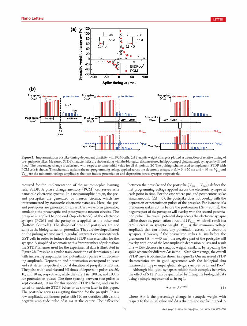
STDP is interpreted as a learning rule that defines how asynapse participates in information processing and brain networkfunctions. According to STDP learning rule, plasticity or so-called synaptic weight depends on the relative timing of pre- andpostsynaptic spikes. The synapse potentiates (increase in synap-tic weight or conductance) if presynaptic spike precedes post-synaptic spike repeatedly, and the synapse depresses (decrease insynaptic weight or conductance) if postsynaptic spike precedespresynaptic spike repeatedly (Figure 2a). The precise pre-/postspike timing window, which controls the sign andmagnitudeof synaptic weight modification, is around 100 ms for biologicalsynapses.8�10 STDP strengthens synapses that receive correlatedinput, which can lead to the formation of stimulus-selectivecolumns and the development of selectivity maps in the brain.11
A conventional version of a STDP circuit built with CMOStechnology includes more than 20 transistors16 which occupy asignificantly larger area than a single element nanoelectronicsynapse. As demonstrated in this work, a very fine control ofintermediate resistance levels in a phase change material is
D dx.doi.org/10.1021/nl201040y |Nano Lett. XXXX, XXX, 000–000
Nano Letters LETTER
required for the implementation of the neuromorphic learningrule, STDP. A phase change memory (PCM) cell serves as ananoscale electronic synapse. In a neuromorphic design, the pre-and postspikes are generated by neuron circuits, which areinterconnected by nanoscale electronic synapses. Here, the pre-and postspikes are generated by an arbitrary waveform generator,emulating the presynaptic and postsynaptic neuron circuits. Theprespike is applied to one end (top electrode) of the electronicsynapse (PCM) and the postspike is applied to the other end(bottom electrode). The shapes of pre- and postspikes are notsame as the biological action potentials. They are developed basedon the pulsing scheme used in gradual set/reset experiments withGST cells in order to induce desired STDP characteristics for thesynapse. A simplified schematic with a fewer number of pulses thanthe STDP schemes used for the experimental data is illustrated inFigure 2b. Prespike is a pulse train, consisting of depression pulseswith increasing amplitudes and potentiation pulses with decreas-ing amplitude. Depression and potentiation correspond to resetand set states, respectively. Total duration of prespike is 120 ms.The pulse width and rise and fall times of depression pulses are 50,10, and 10 ns, respectively, while they are 1 μs, 100 ns, and 100 nsfor potentiation pulses. The time spacing between two pulses iskept constant, 10 ms for this specific STDP scheme, and can betuned to modulate STDP behavior as shown later in this paper.The postspike serves as a gating function for the prespike. It is alow amplitude, continuous pulse with 120 ms duration with a shortnegative amplitude pulse of 8 ms at the center. The difference
between the prespike and the postspike (Vpre � Vpost) defines thenet programming voltage applied across the electronic synapse ateach point in time. For the case where pre- and postneurons spikesimultaneously (Δt = 0), the postspike does not overlap with thedepression or potentiation pulses of the prespike. For instance, if apreneuron spikes 20 ms before the postneuron (Δt = 20 ms), thenegative part of the postspike will overlap with the second potentia-tion pulse. The overall potential drop across the electronic synapsewill be above the potentiation threshold (Vpmin), whichwill result in a60% increase in synaptic weight. Vpmin is the minimum voltageamplitude that can induce any potentation across the electronicsynapses. However, if the postneuron spikes 40 ms before thepreneuron (Δt = �40 ms), the negative part of the postspike willoverlap with one of the low amplitude depression pulses and resultin a �15% decrease in synaptic weight. Similarly, by repeating thespike scheme for differentΔts in the�50 to 50ms range, the overallSTDPcurve is obtained as shown inFigure 2a.Ourmeasured STDPcharacteristics are in good agreement with the biological datameasured in hippocampal glutamatergic synapses by Bi and Poo.8
Although biological synapses exhibit much complex behavior,the effect of STDP can be quantified by fitting the biological datausing a simple exponential as in eq 1.
Δw ¼ Ae�Δt=τ ð1Þ
where Δw is the percentage change in synaptic weight withrespect to the initial value andΔt is the pre-/postspike interval. A
Figure 2. Implementation of spike-timing-dependent plasticity with PCM cells. (a) Synaptic weight change is plotted as a function of relative timing ofpre- and postspikes. Measured STDP characteristics are shown along with the biological data measured in hippocampal glutamatergic synapses by Bi andPoo.8 The percentage change is calculated with respect to same initial value for all Δt points. (b) The pulsing scheme used to implement STDP withPCM cells is shown. The schematic explains the net programming voltage applied across the electronic synapse atΔt = 0,þ20ms, and�40ms.Vpmin andVdmin
are the minimum voltage amplitudes that can induce potentiation and depression across synapse, respectively.
E dx.doi.org/10.1021/nl201040y |Nano Lett. XXXX, XXX, 000–000
Nano Letters LETTER
and τ are two free parameters found by fitting the data. A and τcorrespond to the scaling factor and the time constant for STDPcurve, respectively. These exponential fits are very convenient toformalize STDP into a simple parametric model to be used incomputational studies. In recent years, biological experimentshave shown that the time constant of the STDP window canshow significant variation depending on the location of thesynapses in the brain.33�38 For instance hippocampal glutama-tergic synapses show potentiation with τ of 16.8 ms while τ forvisual cortex neurons is measured as 13.3 ms. It is commonlybelieved that synapses with different τ may serve specific func-tions in information processing at different stages of neuralpathways. The electronic synapses capturing this variation inSTDP characteristics of biological synapses can bring anotherdegree of freedom for designing complex cognitive systems inthe future. Control of τ can be achieved by modifying theamplitude and the time spacing between the individual pulsesin the prespike. As shown in Figure 2b, the pulses in prespike areequally spaced and the pulse amplitude increases or decreaseslinearly. We can decrease the spacing between the pulses with thesmallest spacing between the two highest amplitude depressionand potentiation pulses. In doing so a sharper change in STDPcharacteristics and, hence, a smaller τ can be obtained. Moreover,an exponential increase and decrease in the amplitude of thedepression and potentiation pulses can be implemented, respec-tively, instead of a linear increase and decrease in the pulseamplitude shown in Figure 2b. In order to show that we cancontrol τ, STDP is measured on electronic synapses by modify-ing the time spacing and amplitude of the pulses in the prespike
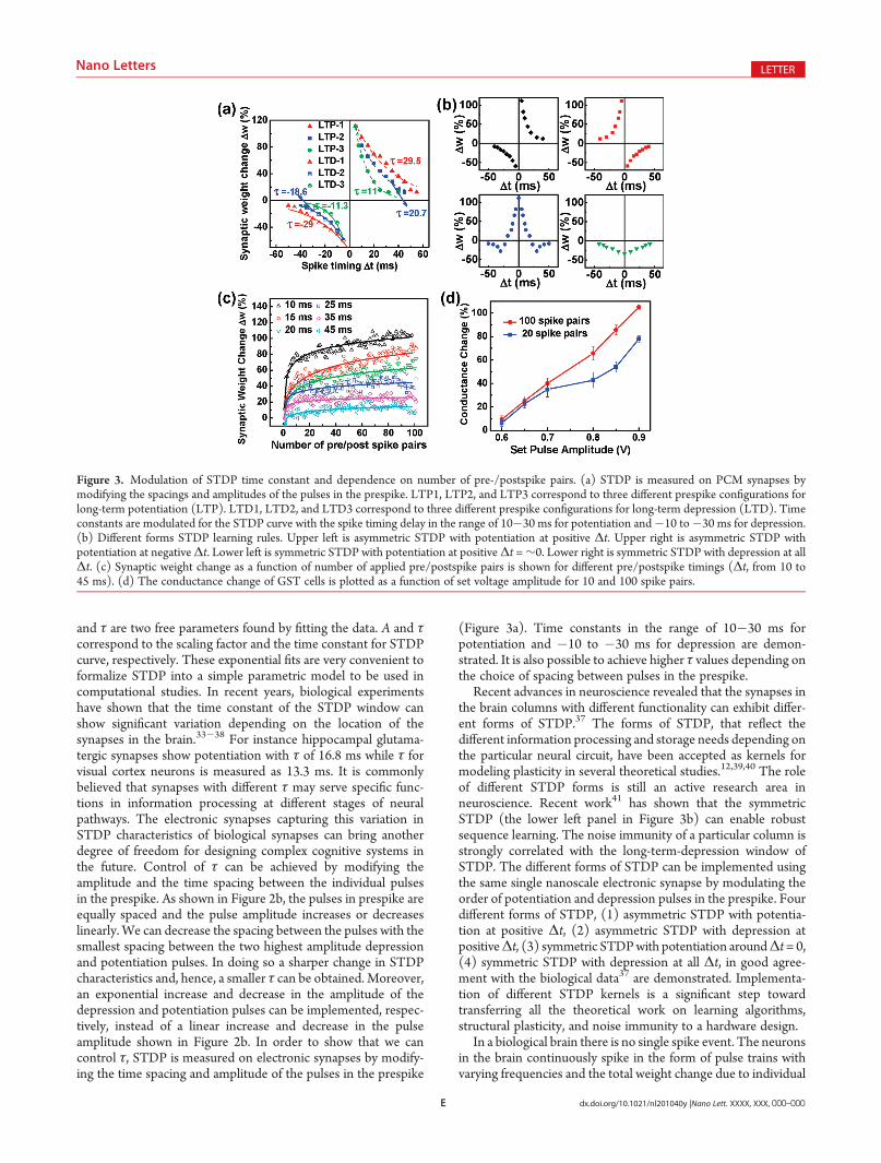
(Figure 3a). Time constants in the range of 10�30 ms forpotentiation and �10 to �30 ms for depression are demon-strated. It is also possible to achieve higher τ values depending onthe choice of spacing between pulses in the prespike.
Recent advances in neuroscience revealed that the synapses inthe brain columns with different functionality can exhibit differ-ent forms of STDP.37 The forms of STDP, that reflect thedifferent information processing and storage needs depending onthe particular neural circuit, have been accepted as kernels formodeling plasticity in several theoretical studies.12,39,40 The roleof different STDP forms is still an active research area inneuroscience. Recent work41 has shown that the symmetricSTDP (the lower left panel in Figure 3b) can enable robustsequence learning. The noise immunity of a particular column isstrongly correlated with the long-term-depression window ofSTDP. The different forms of STDP can be implemented usingthe same single nanoscale electronic synapse by modulating theorder of potentiation and depression pulses in the prespike. Fourdifferent forms of STDP, (1) asymmetric STDP with potentia-tion at positive Δt, (2) asymmetric STDP with depression atpositiveΔt, (3) symmetric STDPwith potentiation aroundΔt= 0,(4) symmetric STDP with depression at all Δt, in good agree-ment with the biological data37 are demonstrated. Implementa-tion of different STDP kernels is a significant step towardtransferring all the theoretical work on learning algorithms,structural plasticity, and noise immunity to a hardware design.
In a biological brain there is no single spike event. The neuronsin the brain continuously spike in the form of pulse trains withvarying frequencies and the total weight change due to individual
Figure 3. Modulation of STDP time constant and dependence on number of pre-/postspike pairs. (a) STDP is measured on PCM synapses bymodifying the spacings and amplitudes of the pulses in the prespike. LTP1, LTP2, and LTP3 correspond to three different prespike configurations forlong-term potentiation (LTP). LTD1, LTD2, and LTD3 correspond to three different prespike configurations for long-term depression (LTD). Timeconstants are modulated for the STDP curve with the spike timing delay in the range of 10�30 ms for potentiation and�10 to�30 ms for depression.(b) Different forms STDP learning rules. Upper left is asymmetric STDP with potentiation at positive Δt. Upper right is asymmetric STDP withpotentiation at negativeΔt. Lower left is symmetric STDP with potentiation at positiveΔt =∼0. Lower right is symmetric STDP with depression at allΔt. (c) Synaptic weight change as a function of number of applied pre/postspike pairs is shown for different pre/postspike timings (Δt, from 10 to45 ms). (d) The conductance change of GST cells is plotted as a function of set voltage amplitude for 10 and 100 spike pairs.
F dx.doi.org/10.1021/nl201040y |Nano Lett. XXXX, XXX, 000–000
Nano Letters LETTER
spike pairs is cumulative. In most of the biological studies, about60�100 pre-/postspike pairs are repeatedly applied for severalminutes to induce long-term potentiation (LTP) or long-termdepression (LTD). The repetition of pre-/postspike pairs resultin a cumulative weight change dependent on the number of spikepairs with a maximum of 100%. The number of pairing eventsrequired to cause a certain amount of potentiation or depressionduring STDP shows variation depending on the type and locationof synapses. For instance in the optic tectum of the tadpole in vivo,while a moderate amount of LTP was induced after 20 pre-/postspike pairs, maximum LTP was reached after 80�200 pre-/postspike pairs.9On the other hand, in the cortex, 15 or fewer pre-/postspike pairs were shown to induce a high level of LTP.42 Therequired number of pre-/postspike pairs is a parameter that needsto be implemented to represent the probability of inducingpotentiation in a neural circuit. In Figure 3c, synaptic weightchange as a function of number of applied pre-/postspike pairs isshown for different pre-/postspike timings (Δt, from 10 to 45ms),measured on the same electronic synapse. A sharp increase in thesynaptic weight change in the first 10�20 spike pairs is followed bya slower increase and saturation close to the 100th spike pair. Themeasured dependence of STDP on number of pre-/postspikepairs for electronic synapses is very similar to the trend observed insome of the synapses in young rat visual cortex.42 These results canbe interpreted as the probability of inducing LTP in synapsesdepends on the number of the spike pair repetitions.
The dependence on number of pre-/postspike pairs forelectronic synapses can be understood from a potentiation pulseamplitude point of view. A synaptic weight increase, which can beinduced by a single pre-/postspike pair, can also be induced by alarger number of pre-/postspike pairs if the amplitude of potentia-tion pulses in STDP scheme is reduced. Lowering the potentiation(set) pulse amplitude results in a smaller fraction of crystallineregion inside the amorphous cap in GST. The crystalline GSTvolume expands as more set pulses are applied repeatedly. Theconductance change of GST cells, extracted from Figure 3c, isplotted as a function of set voltage amplitude for 20 and 100 spikepairs in Figure 3d. It can be seen that to achieve the sameconductance change, the smaller amplitude spikes require a largernumber of repetition pairs. This characteristic of the phase changematerials allows for including the number of spike pairs as a
parameter in cognitive system design while covering the requiredrange measured in biological experiments.
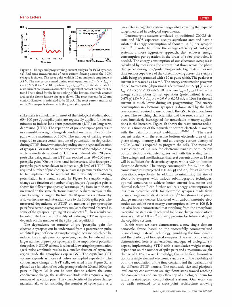
Neuromorphic systems emulated by traditional CMOS cir-cuits and MOS capacitors occupy significant area and have asubstantial energy consumption of about ∼10�9 J per synapticevent.43 In order to mimic the energy efficiency of biologicalsystems, a more aggressive approach, that achieves energyconsumption per operation in the order of a few picojoules, isneeded. The energy consumption of our electronic synapses iscalculated by measuring the current that flows across the phasechange cell during pre-/postspiking events. Figure 4a shows realtime oscilloscope trace of the current flowing across the synapsewhile being programmed with a 10 ns pulse width. The peak resetcurrent is measured as 1.8 mA. The energy consumed to programthe cell to reset state (depression) is determined as∼50 pJ (E=V�Iavg� t = 5.5 V� 0.9 mA� 10 ns, where Iavg = Ipeak/2), while theenergy consumption for set operation (potentiation) is only0.675 pJ (E =V� Iavg� t = 0.9 V� 0.075mA� 10 ns) as the cellcurrent is much lower during set programming. The energyconsumption in electronic synapses is dominated by the highreset current required to melt-quench the GST to its amorphousphase. The switching characteristics and the reset current havebeen intensively investigated for nonvolatile memory applica-tions in the literature. Figure 4b shows the reset current reduc-tion as a function of the equivalent bottom electrode diameter,with the data from recent publications.24,26,44�54 The resetcurrent scales with the effective bottom electrode area of thephase change memory cells and an average current density of∼20MA/cm2 is required to program the cells. The measuredreset current of 1.8 mA for electronic synapses with 75 nmbottom electrode diameter agrees well with this scaling trend.The scaling trend line illustrates that reset currents as low as 25 μAwill be sufficient for electronic synapses with a <20 nm bottomelectrode diameter. The energy consumption for <20 nm elec-tronic synapses is projected as 0.027 pJ and 2 pJ for set and resetoperations, respectively. In addition to minimizing the size ofelectronic synapses with various sublithographic techniques,optimal structures to achieve better current localization andthermal isolation54 can further reduce energy consumption toless than picojoule levels for electronic synapses made fromphase change materials. A recent study55 has shown that phasechange memory devices fabricated with carbon nanotube elec-trodes can exhibit reset energy consumption as low as 100 fJ. Ithas also been demonstrated that switching from the amorphousto crystalline state can be achieved for phase change nanoparticlesizes as small as 1.8 nm56 showing promise for future scaling ofthe cognitive systems.
In this work we have demonstrated a new single elementnanoscale device, based on the successfully commercializedphase change material technology, emulating the functionalityand the plasticity of biological synapses. The electronic synapsedemonstrated here is an excellent analogue of biological sy-napses, implementing STDP with a cumulative weight changedependent on the number of spike pairs and a maximum weightchange of 100%. To our knowledge, this is the first demonstra-tion of a single element electronic synapse with the capability ofboth the modulation of the time constant and the realization ofthe different STDP kernels. The nanoscale size and picojoulelevel energy consumption are significant steps toward reachingthe compactness and energy efficiency of a biological brain forfuture brain-inspired computational systems. Our work canbe easily extended to a cross-point architecture allowing
Figure 4. Energy and programming current analysis for PCM synapse.(a) Real time measurement of reset current flowing across the PCMsynapse is shown. The reset pulse width is 10 ns and pulse amplitude is5.5 V. The energy consumed during reset operation is E = V � Iavg �t = 5.5 V� 0.9 mA� 10 ns, where Iavg = Ipeak/2. (b) Literature data forreset current are shown as a function of equivalent contact diameter. Thetrend line is fitted for the linear scaling of the bottom electrode contactarea as the device feature size goes down. The reset current for 20 nmcontact diameter is estimated to be 25 μA. The reset current measuredon PCM synapse is shown with the green star symbol.
G dx.doi.org/10.1021/nl201040y |Nano Lett. XXXX, XXX, 000–000
Nano Letters LETTER
three-dimensional stacking of many layers of electronic synapses,thereby enabling us to approach the massive parallelism ofthe brain.
’ASSOCIATED CONTENT
bS Supporting Information. Phase change synaptic devicefabrication, basic electrical characterization of fabricated devices,measurement setup for implementation of synaptic plasticity,and details of finite element simulations for gradual resistancechange. This material is available free of charge via the Internet athttp://pubs.acs.org.
’AUTHOR INFORMATION
Corresponding Author*E-mail: [email protected].
’ACKNOWLEDGMENT
The authors thank Prof. Kwabena Boahen for useful discussions,Jiale Liang for her helpwith reset current analysis and SangbumKimfor his help in device fabrication. This work is supported byDARPASyNAPSE (DSO Program Manager T. Hylton), the NationalScience Foundation (NSF, ECCS 0950305), the NanoelectronicsResearch Initiative (NRI) of the Semiconductor Research Corpora-tion through the NSF/NRI Supplement to the NSF NSEC Centerfor Probing the Nanoscale (CPN).
’REFERENCES
(1) Special Issue Proc. IEEE 2008, 96, 2.(2) Borwein, J.M.; Borwein, P. B., Pi and the AGM : a study in analytic
number theory and computational complexity; Wiley: New York, 1987.(3) DARPA/DSO BAA08-28. Systems of Neuromorphic Adaptive
Plastic Scalable Electronics (SyNAPSE), www.darpa.mil/dso/solicita-tions/BAA08-28.pdf.(4) IBM unveils a new brain simulator, IEEE Spectrum, Nov 2009.(5) Drachman, D. Neurology 2005, 64, 2004�2005.(6) Dan, Y.; Poo, M. M. Physiol. Rev. 2006, 86, 1033�1048.(7) Hebb, D. The organization of behavior; a neuropsychological
theory; Wiley: New York, 1949.(8) Bi, G. Q.; Poo, M. M. J. Neurosci. 1998, 18, 10464�10472.(9) Zhang, L. I.; Tao, H. W.; Holt, C. E.; Harris, W. A.; Poo, M. M.
Nature 1998, 395, 37�44.(10) Markram, H.; Lubke, J.; Frotscher, M.; Sakmann, B. Science
1997, 275, 213�215.(11) Song, S.; Abbott, L. F. Neuron 2001, 32, 339�350.(12) Song, S.; Miller, K. D.; Abbott, L. F. Nat. Neurosci. 2000,
3, 919�926.(13) Van Rossum, M. C. W.; Bi, G. Q.; Turrigiano, G. G. J. Neurosci.
2000, 20, 8812�8821.(14) Brader, J. M.; Senn, W.; Fusi, S. Neural Comput. 2007,
19, 2881�2912.(15) Arthur, J.; Boahen, K. Adv. Neural Inf. Process. Syst. 2006,
18, 75�82.(16) Joshi, J.; Parker, A. C.; Hsu, C.-C. Conf. Proc. IEEE Eng. Med.
Biol. Soc. 2009, 1651�1654.(17) Tanaka, H.; Morie, T.; Aihara, K. Int. Congr. Ser. 2007,
1301, 152�155.(18) Snider, G. S. IEEE/ACM Int. Symp. Nanoscale Architectures
2008, 85�92.(19) Jo, S. H.; Chang, T.; Ebong, I.; Bhadviya, B. B.; Mazumder, P.;
Lu, W. Nano Lett. 2010, 10, 1297�1301.
(20) Alibart, F.; Pleutin, S.; Geurin, D.; Novembre, C.; Lenfant, S.;Lmimouni, K.; Gamrat, C.; Vuillaume, D. Adv. Funct. Mater. 2010,20, 330�337.
(21) Lai, S. IEDM ’03 Tech. Dig. 2003, 10.1.1�10.1.4.(22) Ovshinsky, S. R. Phys. Rev. Lett. 1968, 21, 1450�1452.(23) Lankhorst, M. H. R.; Ketelaars, B. W. S. M. M.; Wolter, R. A.
Nat. Mater. 2005, 4, 347�352.(24) Servalli, G. IEDM ’09 Tech. Dig. 2009, 5.7.1�5.7.4.(25) Bez, R. IEDM ’09 Tech. Dig. 2009, 5.1.1�5.1.4.(26) Oh, J. H.; Park, J. H.; Lim, Y. S.; Lim, H. S.; Oh, Y. T.; Kim, J. S.;
Shin, J. M.; Song, Y. J.; Ryoo, K. C.; Lim, D. W.; Park, S. S.; Kim, J. I.;Kim, J. H.; Yu, J.; Yeung, F.; Jeong, C.W.; Kong, J. H.; Kang, D. H.; Koh,G. H.; Jeong, G. T.; Jeong, H. S.; Kim, K. IEDM ’06 Tech. Dig.2006, 49�53.
(27) Villa, C.; Mills, D.; Barkley, G.; Giduturi, H.; Schippers, S.;Vimercati, D. ISSCC 2010.
(28) Raoux, S. Annu. Rev. Mater. Res. 2009, 39, 25�48.(29) Nakayama, K.; Takata, M.; Kasai, T.; Kitagawa, A.; Akita, J. J.
Phys. D: Appl. Phys. 2007, 40, 5061�5065.(30) Nirschl, T.; Phipp, J. B.; Happ, T. D.; Burr, G. W.; Rajendran,
B.; Lee, M.-H.; Schrott, A.; Yang, M.; Breitwisch, M.; Chen, C.-F.;Joseph, E.; Lamorey, M.; Cheek, R.; Chen, S.-H.; Zaidi, S.; Raoux, S.;Chen, Y. C.; Zhu, Y.; Bergmann, R.; Lung, H.-L.; Lam, C. IEDM’07 Tech.Dig. 2007, 461�464.
(31) Ielmini, D.; Lacaita, A. L.; Pirovano, A.; Pellizzer, F.; Bez, R.IEEE Electron Device Lett. 2004, 25, 507�509.
(32) Multiphysics and Simulation Software: COMSOL. http://www.comsol.com/
(33) Bi, G.; Poo, M. Annu. Rev. Neurosci. 2001, 24, 139�166.(34) Froemke, R. C.; Dan, Y. Nature 2002, 416, 433�438.(35) Levy, W.; Steward, O. Neuroscience 1983, 8, 791�797.(36) Pratt, K.; Dong, W.; Aizenman, C. Nat. Neurosci. 2008,
11, 467�475.(37) Wittenberg, G.; Wang, S. J. Neurosci. 2006, 26, 6610�6617.(38) Zhang, X.; Zhang, J.; Chen, C. Biochem. Biophys. Res. Commun.
2009, 383, 326�330.(39) Cassenaer, S.; Laurent, G. Nature 2007, 448, 709�713.(40) Fiete, I. R.; Senn, W.; Wang, C. H. Z.; Hahnloser, R. H. R.
Neuron 2010, 65, 563�576.(41) Hayashi, H.; Igarashi, J. Cognit. Neurodyn. 2009, 3, 119�130.(42) Froemke, R. C.; Tsay, I. A.; Raad, M.; Long, J. D.; Dan, Y. J.
Neurophysiol. 2006, 95, 1620�1629.(43) Indiveri, G.; Chicca, E.; Douglas, R. IEEE Trans. Neural Net.
2006, 17, 211�221.(44) Pirovano, A.; Lacaita, A. L.; Benvenuti, A.; Pellizzer, F.; Hudgens,
S.; Bez, R. IEDM ’03 Tech. Dig. 2003, 29.6.1�29.6.4.(45) Sasago, Y.; Kinoshita, M.; Morikawa, T.; Kurotsuchi, K.;
Hanzawa, S.; Mine, T.; Shima, A.; Fujisaki, Y.; Kume, H.; Moriya, H.;Takaura, N.; Torii, K. Symp. VLSI Technol., Dig. Tech. Pap. 2009, 24�25.
(46) Ha, Y. H.; Yi, J. H.; Horii, H.; Park, J. H.; Joo, S. H.; Park, S. O.;U-In Chung; Moon, J. T. Symp. VLSI Technol., Dig. Tech. Pap.2003, 175�176.
(47) Pellizzer, F.; Benvenuti, A.; Gleixner, B.; Kim, Y.; Johnson, B.;Magistretti, M.; Marangon, T.; Pirovano, A.; Bez, R.; Atwood, G. Symp.VLSI Technol., Dig. Tech. Pap. 2006, 122�123.
(48) Chen, W. S.; Lee, C.; Chao, D. S.; Chen, Y. C.; Chen, F.; Chen,C.W.; Yen, R.; Chen, M. J.; Wang, W. H.; Hsiao, T. C.; Yeh, J. T.; Chiou,S. H.; Liu, M. Y.; Wang, T. C.; Chein, L. L.; Huang, C.; Shih, N. T.; Tu,L. S.; Huang, D.; Yu, T. H.; Kao, M. J.; Tsai, M.-J. IEDM ’07 Tech. Dig.2007, 319�322.
(49) Pirovano, A.; Pellizzer, F.; Tortorelli, I.; Harrigan, R.; Magistretti,M.; Petruzza, P.; Varesi, E.; Erbetta, D.; Marangon, T.; Bedeschi, F.;Fackenthal, R.; Atwood, G.; Bez, R. 37th ESSDERC 2007, 222�225.
(50) Breitwisch, M.; Nirschl, T.; Chen, C. F.; Zhu, Y.; Lee, M. H.;Lamorey, M.; Burr, G. W.; Joseph, E.; Schrott, A.; Philipp, J. B.; Cheek,R.; Happ, T. D.; Chen, S. H.; Zaidr, S.; Flaitz, P.; Bruley, J.; Dasaka, R.;Rajendran, B.; Rossnage, S.; Yang, M.; Chen, Y. C.; Bergmann, R.; Lung,H. L.; Lam, C. Symp. VLSI Technol., Dig. Tech. Pap. 2007, 100�101.
H dx.doi.org/10.1021/nl201040y |Nano Lett. XXXX, XXX, 000–000
Nano Letters LETTER
(51) Ahn, S. J.; Hwang, Y. N.; Song, Y. J.; Lee, S. H.; Lee, S. Y.; Park,J. H.; Jeong, C.W.; Ryoo, K. C.; Shin, J. M.; Fai, Y.; Oh, J. H.; Koh, G. H.;Jeong, G. T.; Joo, S. H.; Choi, S. H.; Son, Y. H.; Shin, J. C.; Kim, Y. T.;Jeong, H. S.; Kim, K. Symp. VLSI Technol., Dig. Tech. Pap. 2005, 98�99.(52) Song, Y. J.; Ryoo, K. C.; Hwang, Y. N.; Jeong, C. W.; Lim,
D. W.; Park, S. S.; Kim, J. I.; Kim, J. H.; Lee, S. Y.; Kong, J. H.; Ahn, S. J.;Lee, S. H.; Park, J. H.; Oh, J. H.; Oh, Y. T.; Kim, J. S.; Shin, J. M.; Fai, Y.;Koh, G. H.; Jeong, G. T.; Kim, R. H.; Lim, H. S.; Park, I. S.; Jeong, H. S.;Kinam Kim Symp. VLSI Technol., Dig. Tech. Pap. 2006, 118�119.(53) Hwang, Y. N.; Lee, S. H.; Ahn, S. J.; Lee, S. Y.; Ryoo, K. C.;
Hong, H. S.; Koo, H. C.; Yeung, F.; Oh, J. H.; Kim, H. J.; Jeong, W. C.;Park, J. H.; Horii, H.; Ha, Y. H.; Yi, J. H.; Koh, G. H.; Jeong, G. T.; Jeong,H. S.; Kinam Kim IEDM ’03 Tech. Dig. 2003, 37.1.1�37.1.4.(54) Lee, J. I.; Park, H.; Cho, S. L.; Park, Y. L.; Bae, B. J.; Park, J. H.;
Park, J. S.; An, H. G.; Bae, J. S.; Ahn, D. H.; Kim, Y. T.; Horii, H.; Song,S. A.; Shin, J. C.; Park, S. O.; Kim, H. S.; U-In Chung; Moon, J. T.; Ryu,B. I. Symp. VLSI Technol., Dig. Tech. Pap. 2007, 102�103.(55) Xiong, F.; Liao, A.; Estrada, D.; Pop, E. Science 2011, DOI:
10.1126/science.1201938.(56) Caldwell, M. A.; Raoux, S.; Wang, R. Y.; Wong, H.-S. P.;
Milliron, D. J. J. Mater. Chem. 2010, 20, 1285�1291.