Nanoelectronic Mixed-Signal System Design
113
Transcript of Nanoelectronic Mixed-Signal System Design


Nanoelectronic Mixed-Signal System Design
Saraju P. Mohanty
Saraju P. MohantyUniversity of North Texas, Denton. e-mail: [email protected]
1
Contents
Nanoelectronic Mixed-Signal System Design . . . . . . . . . . . . . . . . . . . . . . . . . . . . . . . . . . . . . . . . . . . . . . . 1
Saraju P. Mohanty
1 Opportunities and Challenges of Nanoscale Technology and Systems . . . . . . . . . . . . . . . . . . . . . . . . 1
1 Introduction . . . . . . . . . . . . . . . . . . . . . . . . . . . . . . . . . . . . . . . . . . . . . . . . . . . . . . . . . . . . . . . . . . . . . 1
2 Mixed-Signal Circuits and Systems . . . . . . . . . . . . . . . . . . . . . . . . . . . . . . . . . . . . . . . . . . . . . . . . . 3
2.1 Different Processors: Electrical to Mechanical . . . . . . . . . . . . . . . . . . . . . . . . . . . . . . . . 3
2.2 Analog Versus Digital Processors . . . . . . . . . . . . . . . . . . . . . . . . . . . . . . . . . . . . . . . . . . . 4
2.3 Analog, Digital, Mixed-Signal Circuits and Systems . . . . . . . . . . . . . . . . . . . . . . . . . . . 4
2.4 Two Types of Mixed-Signal Systems . . . . . . . . . . . . . . . . . . . . . . . . . . . . . . . . . . . . . . . . 4
3 Nanoscale CMOS Circuit Technology . . . . . . . . . . . . . . . . . . . . . . . . . . . . . . . . . . . . . . . . . . . . . . . 6
3.1 Developmental Trend . . . . . . . . . . . . . . . . . . . . . . . . . . . . . . . . . . . . . . . . . . . . . . . . . . . . . 6
3.2 Nanoscale CMOS Alternative Device Options . . . . . . . . . . . . . . . . . . . . . . . . . . . . . . . . 6
3.3 Advantage and Disadvantages of Technology Scaling . . . . . . . . . . . . . . . . . . . . . . . . . . 9
3.4 Challenges in Nanoscale Design . . . . . . . . . . . . . . . . . . . . . . . . . . . . . . . . . . . . . . . . . . . . 9
4 Power Consumption and Leakage Dissipation Issues in AMS-SoCs . . . . . . . . . . . . . . . . . . . . . . 10
4.1 Power Consumption in Various Components in AMS-SoCs . . . . . . . . . . . . . . . . . . . . . 10
4.2 Power and Leakage Trend in Nanoscale Technology . . . . . . . . . . . . . . . . . . . . . . . . . . . 10
4.3 The Impact of Power Consumption and Leakage Dissipation . . . . . . . . . . . . . . . . . . . . 11
5 Parasitics Issue . . . . . . . . . . . . . . . . . . . . . . . . . . . . . . . . . . . . . . . . . . . . . . . . . . . . . . . . . . . . . . . . . . 12
5.1 Types of Parasitics . . . . . . . . . . . . . . . . . . . . . . . . . . . . . . . . . . . . . . . . . . . . . . . . . . . . . . . . 12
5.2 The Impact of Parasitics . . . . . . . . . . . . . . . . . . . . . . . . . . . . . . . . . . . . . . . . . . . . . . . . . . . 12
5.3 Challenges to Account Parasitics during Design . . . . . . . . . . . . . . . . . . . . . . . . . . . . . . . 14
6 Nanoscale Circuit Process Variation Issues . . . . . . . . . . . . . . . . . . . . . . . . . . . . . . . . . . . . . . . . . . . 14
6.1 Types of Process Variation . . . . . . . . . . . . . . . . . . . . . . . . . . . . . . . . . . . . . . . . . . . . . . . . . 14
6.2 The Impact of Process Variation . . . . . . . . . . . . . . . . . . . . . . . . . . . . . . . . . . . . . . . . . . . . 14
7 The Temperature Variation Issue . . . . . . . . . . . . . . . . . . . . . . . . . . . . . . . . . . . . . . . . . . . . . . . . . . . . 15
7.1 The Issue of Temperature . . . . . . . . . . . . . . . . . . . . . . . . . . . . . . . . . . . . . . . . . . . . . . . . . . 15
7.2 The Impact of Temperature . . . . . . . . . . . . . . . . . . . . . . . . . . . . . . . . . . . . . . . . . . . . . . . . 16
7.3 Challenges to Account through PVT-Aware Design . . . . . . . . . . . . . . . . . . . . . . . . . . . . 16
8 Challenges in Nanoscale CMOS AMS-SoC Design . . . . . . . . . . . . . . . . . . . . . . . . . . . . . . . . . . . . 17
8.1 AMS-SoC Design Flow . . . . . . . . . . . . . . . . . . . . . . . . . . . . . . . . . . . . . . . . . . . . . . . . . . . 17
8.2 AMS-SoC Unified Optimization . . . . . . . . . . . . . . . . . . . . . . . . . . . . . . . . . . . . . . . . . . . . 18
9 Tools for Mixed-Signal Circuit Design . . . . . . . . . . . . . . . . . . . . . . . . . . . . . . . . . . . . . . . . . . . . . . 19
9.1 The AMS-SoC Design Issue . . . . . . . . . . . . . . . . . . . . . . . . . . . . . . . . . . . . . . . . . . . . . . . 19
9.2 Languages for AMS-SoC Design . . . . . . . . . . . . . . . . . . . . . . . . . . . . . . . . . . . . . . . . . . . 19
9.3 Tools for AMS-SoC Design and Simulation . . . . . . . . . . . . . . . . . . . . . . . . . . . . . . . . . . 21
9.4 Transistor Models . . . . . . . . . . . . . . . . . . . . . . . . . . . . . . . . . . . . . . . . . . . . . . . . . . . . . . . . 21
References . . . . . . . . . . . . . . . . . . . . . . . . . . . . . . . . . . . . . . . . . . . . . . . . . . . . . . . . . . . . . . . . . . . . . . . . . . . . 23
xiii
xiv Contents
2 Emerging Systems Designed as Analog / Mixed-Signal System-on-Chips (AMS-SoCs) . . . . . . . . . 29
10 Introduction . . . . . . . . . . . . . . . . . . . . . . . . . . . . . . . . . . . . . . . . . . . . . . . . . . . . . . . . . . . . . . . . . . . . . 29
11 Atomic Force Microscope (AFM). . . . . . . . . . . . . . . . . . . . . . . . . . . . . . . . . . . . . . . . . . . . . . . . . . . 29
11.1 AFM: What Is It? . . . . . . . . . . . . . . . . . . . . . . . . . . . . . . . . . . . . . . . . . . . . . . . . . . . . . . . . 29
11.2 AFM: Background . . . . . . . . . . . . . . . . . . . . . . . . . . . . . . . . . . . . . . . . . . . . . . . . . . . . . . . 29
11.3 AFM: What is Inside? . . . . . . . . . . . . . . . . . . . . . . . . . . . . . . . . . . . . . . . . . . . . . . . . . . . . . 30
12 Biosensor Systems . . . . . . . . . . . . . . . . . . . . . . . . . . . . . . . . . . . . . . . . . . . . . . . . . . . . . . . . . . . . . . . 31
12.1 Biosensor: What Is It? . . . . . . . . . . . . . . . . . . . . . . . . . . . . . . . . . . . . . . . . . . . . . . . . . . . . . 31
12.2 Biosensor Systems: Background . . . . . . . . . . . . . . . . . . . . . . . . . . . . . . . . . . . . . . . . . . . . 34
12.3 Biosensor Systems: What is Inside? . . . . . . . . . . . . . . . . . . . . . . . . . . . . . . . . . . . . . . . . . 34
13 Blu-ray Player . . . . . . . . . . . . . . . . . . . . . . . . . . . . . . . . . . . . . . . . . . . . . . . . . . . . . . . . . . . . . . . . . . . 35
13.1 Blu-ray Player: What Is It? . . . . . . . . . . . . . . . . . . . . . . . . . . . . . . . . . . . . . . . . . . . . . . . . . 35
13.2 Home Video Systems Background: From Video Cassette Player to Blu-ray Player . . 36
13.3 Blu-ray Player: What Is Inside? . . . . . . . . . . . . . . . . . . . . . . . . . . . . . . . . . . . . . . . . . . . . . 36
14 Drug-Delivery Nano-Electro-Mechanical Systems (DDNEMS) . . . . . . . . . . . . . . . . . . . . . . . . . . 37
14.1 DDNEMS: What Is It? . . . . . . . . . . . . . . . . . . . . . . . . . . . . . . . . . . . . . . . . . . . . . . . . . . . . 37
14.2 Drug-Delivery Systems: Background . . . . . . . . . . . . . . . . . . . . . . . . . . . . . . . . . . . . . . . . 37
14.3 DDNEMS: What Is Inside? . . . . . . . . . . . . . . . . . . . . . . . . . . . . . . . . . . . . . . . . . . . . . . . . 38
15 Digital Video Recorder (DVR) . . . . . . . . . . . . . . . . . . . . . . . . . . . . . . . . . . . . . . . . . . . . . . . . . . . . . 39
15.1 DVR: What Is It? . . . . . . . . . . . . . . . . . . . . . . . . . . . . . . . . . . . . . . . . . . . . . . . . . . . . . . . . . 39
15.2 DVR: Background . . . . . . . . . . . . . . . . . . . . . . . . . . . . . . . . . . . . . . . . . . . . . . . . . . . . . . . . 40
15.3 DVR: What Is Inside? . . . . . . . . . . . . . . . . . . . . . . . . . . . . . . . . . . . . . . . . . . . . . . . . . . . . . 40
16 Electroencephalogram (EEG) System . . . . . . . . . . . . . . . . . . . . . . . . . . . . . . . . . . . . . . . . . . . . . . . 41
16.1 EEG System: What Is It? . . . . . . . . . . . . . . . . . . . . . . . . . . . . . . . . . . . . . . . . . . . . . . . . . . 41
16.2 EEG System: Background . . . . . . . . . . . . . . . . . . . . . . . . . . . . . . . . . . . . . . . . . . . . . . . . . 41
16.3 EEG System: What Is Inside? . . . . . . . . . . . . . . . . . . . . . . . . . . . . . . . . . . . . . . . . . . . . . . 41
17 GPS Navigation Device . . . . . . . . . . . . . . . . . . . . . . . . . . . . . . . . . . . . . . . . . . . . . . . . . . . . . . . . . . . 42
17.1 GPS Device: What Is It? . . . . . . . . . . . . . . . . . . . . . . . . . . . . . . . . . . . . . . . . . . . . . . . . . . . 42
17.2 GPS Device: Background . . . . . . . . . . . . . . . . . . . . . . . . . . . . . . . . . . . . . . . . . . . . . . . . . . 42
17.3 GPS Device: What Is Inside? . . . . . . . . . . . . . . . . . . . . . . . . . . . . . . . . . . . . . . . . . . . . . . . 42
18 GPU-CPU Hybrid (GCH) System . . . . . . . . . . . . . . . . . . . . . . . . . . . . . . . . . . . . . . . . . . . . . . . . . . 43
18.1 GCH: What Is It? . . . . . . . . . . . . . . . . . . . . . . . . . . . . . . . . . . . . . . . . . . . . . . . . . . . . . . . . . 43
18.2 Graphics Processing: Background . . . . . . . . . . . . . . . . . . . . . . . . . . . . . . . . . . . . . . . . . . . 44
18.3 GCH: What Is Inside? . . . . . . . . . . . . . . . . . . . . . . . . . . . . . . . . . . . . . . . . . . . . . . . . . . . . . 45
19 Networked Media Tank (NMT) . . . . . . . . . . . . . . . . . . . . . . . . . . . . . . . . . . . . . . . . . . . . . . . . . . . . . 47
19.1 NMT: What Is It? . . . . . . . . . . . . . . . . . . . . . . . . . . . . . . . . . . . . . . . . . . . . . . . . . . . . . . . . 47
19.2 NMT: Background . . . . . . . . . . . . . . . . . . . . . . . . . . . . . . . . . . . . . . . . . . . . . . . . . . . . . . . 47
19.3 NMT: What Is Inside? . . . . . . . . . . . . . . . . . . . . . . . . . . . . . . . . . . . . . . . . . . . . . . . . . . . . 47
20 Net-Centric Multimedia Processor (NMP) . . . . . . . . . . . . . . . . . . . . . . . . . . . . . . . . . . . . . . . . . . . . 48
20.1 NMP: What Is It? . . . . . . . . . . . . . . . . . . . . . . . . . . . . . . . . . . . . . . . . . . . . . . . . . . . . . . . . 48
20.2 NMP: Background . . . . . . . . . . . . . . . . . . . . . . . . . . . . . . . . . . . . . . . . . . . . . . . . . . . . . . . 49
20.3 NMP: What Is Inside? . . . . . . . . . . . . . . . . . . . . . . . . . . . . . . . . . . . . . . . . . . . . . . . . . . . . . 50
21 Radiation Detection System (RDS) . . . . . . . . . . . . . . . . . . . . . . . . . . . . . . . . . . . . . . . . . . . . . . . . . 51
21.1 RDS: What Is It? . . . . . . . . . . . . . . . . . . . . . . . . . . . . . . . . . . . . . . . . . . . . . . . . . . . . . . . . . 51
21.2 RDS: Background . . . . . . . . . . . . . . . . . . . . . . . . . . . . . . . . . . . . . . . . . . . . . . . . . . . . . . . . 51
21.3 RDS: What Is Inside? . . . . . . . . . . . . . . . . . . . . . . . . . . . . . . . . . . . . . . . . . . . . . . . . . . . . . 52
22 Radio Frequency Identification (RFID) Chip . . . . . . . . . . . . . . . . . . . . . . . . . . . . . . . . . . . . . . . . . 53
22.1 RFID Chip: What Is It? . . . . . . . . . . . . . . . . . . . . . . . . . . . . . . . . . . . . . . . . . . . . . . . . . . . . 53
22.2 RFID Chip: Background . . . . . . . . . . . . . . . . . . . . . . . . . . . . . . . . . . . . . . . . . . . . . . . . . . . 54
22.3 RFID Chip: What Is Inside? . . . . . . . . . . . . . . . . . . . . . . . . . . . . . . . . . . . . . . . . . . . . . . . . 55
23 Secure Digital Camera (SDC) . . . . . . . . . . . . . . . . . . . . . . . . . . . . . . . . . . . . . . . . . . . . . . . . . . . . . . 57
23.1 SDC: What Is It? . . . . . . . . . . . . . . . . . . . . . . . . . . . . . . . . . . . . . . . . . . . . . . . . . . . . . . . . . 57
23.2 SDC: Background . . . . . . . . . . . . . . . . . . . . . . . . . . . . . . . . . . . . . . . . . . . . . . . . . . . . . . . . 57
23.3 SDC: What Is Inside? . . . . . . . . . . . . . . . . . . . . . . . . . . . . . . . . . . . . . . . . . . . . . . . . . . . . . 58
Contents xv
24 Set-Top Box (STB) . . . . . . . . . . . . . . . . . . . . . . . . . . . . . . . . . . . . . . . . . . . . . . . . . . . . . . . . . . . . . . . 59
24.1 STB: What Is It? . . . . . . . . . . . . . . . . . . . . . . . . . . . . . . . . . . . . . . . . . . . . . . . . . . . . . . . . . 59
24.2 STB: Background . . . . . . . . . . . . . . . . . . . . . . . . . . . . . . . . . . . . . . . . . . . . . . . . . . . . . . . . 59
24.3 STB: What Is Inside? . . . . . . . . . . . . . . . . . . . . . . . . . . . . . . . . . . . . . . . . . . . . . . . . . . . . . 59
25 Slate Personal Computer (SPC) . . . . . . . . . . . . . . . . . . . . . . . . . . . . . . . . . . . . . . . . . . . . . . . . . . . . 60
25.1 Slate PC: What Is It? . . . . . . . . . . . . . . . . . . . . . . . . . . . . . . . . . . . . . . . . . . . . . . . . . . . . . . 60
25.2 Slate PC Background: The Developmental Trend of General Purpose Computer
Reaches at Slate PC. . . . . . . . . . . . . . . . . . . . . . . . . . . . . . . . . . . . . . . . . . . . . . . . . . . . . . . 61
25.3 Slate PC: What Is Inside? . . . . . . . . . . . . . . . . . . . . . . . . . . . . . . . . . . . . . . . . . . . . . . . . . . 62
26 Smart Mobile Phone . . . . . . . . . . . . . . . . . . . . . . . . . . . . . . . . . . . . . . . . . . . . . . . . . . . . . . . . . . . . . . 63
26.1 Smart Phone: What Is It? . . . . . . . . . . . . . . . . . . . . . . . . . . . . . . . . . . . . . . . . . . . . . . . . . . 63
26.2 Smart Phone: Background . . . . . . . . . . . . . . . . . . . . . . . . . . . . . . . . . . . . . . . . . . . . . . . . . 64
26.3 Smart Phone: What Is Inside? . . . . . . . . . . . . . . . . . . . . . . . . . . . . . . . . . . . . . . . . . . . . . . 64
27 Software Defined Radio (SDR) . . . . . . . . . . . . . . . . . . . . . . . . . . . . . . . . . . . . . . . . . . . . . . . . . . . . . 64
27.1 SDR: What Is It? . . . . . . . . . . . . . . . . . . . . . . . . . . . . . . . . . . . . . . . . . . . . . . . . . . . . . . . . . 64
27.2 SDR: Background . . . . . . . . . . . . . . . . . . . . . . . . . . . . . . . . . . . . . . . . . . . . . . . . . . . . . . . . 65
27.3 SDR: What Is Inside? . . . . . . . . . . . . . . . . . . . . . . . . . . . . . . . . . . . . . . . . . . . . . . . . . . . . . 66
28 TV Tuner Card for PCs . . . . . . . . . . . . . . . . . . . . . . . . . . . . . . . . . . . . . . . . . . . . . . . . . . . . . . . . . . . 66
28.1 TV Tuner Card: What Is It? . . . . . . . . . . . . . . . . . . . . . . . . . . . . . . . . . . . . . . . . . . . . . . . . 66
28.2 TV Tuner Card: Background . . . . . . . . . . . . . . . . . . . . . . . . . . . . . . . . . . . . . . . . . . . . . . . 67
28.3 TV Tuner Card: What Is Inside? . . . . . . . . . . . . . . . . . . . . . . . . . . . . . . . . . . . . . . . . . . . . 68
29 Universal Remote Control . . . . . . . . . . . . . . . . . . . . . . . . . . . . . . . . . . . . . . . . . . . . . . . . . . . . . . . . . 68
29.1 Universal Remote: What Is It? . . . . . . . . . . . . . . . . . . . . . . . . . . . . . . . . . . . . . . . . . . . . . . 68
29.2 Universal Remote: Background . . . . . . . . . . . . . . . . . . . . . . . . . . . . . . . . . . . . . . . . . . . . . 69
29.3 Universal Remote: What Is Inside? . . . . . . . . . . . . . . . . . . . . . . . . . . . . . . . . . . . . . . . . . . 69
References . . . . . . . . . . . . . . . . . . . . . . . . . . . . . . . . . . . . . . . . . . . . . . . . . . . . . . . . . . . . . . . . . . . . . . . . . . . . 71
3 Nanoelectronics Issues for Design for Excellence . . . . . . . . . . . . . . . . . . . . . . . . . . . . . . . . . . . . . . . . . . 75
30 Introduction . . . . . . . . . . . . . . . . . . . . . . . . . . . . . . . . . . . . . . . . . . . . . . . . . . . . . . . . . . . . . . . . . . . . . 75
31 Design for eXcellence (DFX) . . . . . . . . . . . . . . . . . . . . . . . . . . . . . . . . . . . . . . . . . . . . . . . . . . . . . . 75
32 Different Types of Nanoelectronic Devices . . . . . . . . . . . . . . . . . . . . . . . . . . . . . . . . . . . . . . . . . . . 77
32.1 Nanoscale Classical SiO2/Polysilicon FET (MOSFET or MOS) . . . . . . . . . . . . . . . . . . 78
32.2 High-κ and Metal-Gate Nonclassical FET (HKMGFET) . . . . . . . . . . . . . . . . . . . . . . . . 80
32.3 Multiple Independent Gate FET (MIGFET) . . . . . . . . . . . . . . . . . . . . . . . . . . . . . . . . . . . 83
32.4 Carbon Nanotube FET (CNTFET) . . . . . . . . . . . . . . . . . . . . . . . . . . . . . . . . . . . . . . . . . . 90
32.5 Graphene FET (GFET) . . . . . . . . . . . . . . . . . . . . . . . . . . . . . . . . . . . . . . . . . . . . . . . . . . . . 92
32.6 Single-Electron Transistor (SET) . . . . . . . . . . . . . . . . . . . . . . . . . . . . . . . . . . . . . . . . . . . 95
32.7 Thin Film Transistor (TFT) . . . . . . . . . . . . . . . . . . . . . . . . . . . . . . . . . . . . . . . . . . . . . . . . 96
32.8 Tunnel FET (TFET) . . . . . . . . . . . . . . . . . . . . . . . . . . . . . . . . . . . . . . . . . . . . . . . . . . . . . . 98
32.9 Vibrating Body Field Effect Transistor (VBFET) . . . . . . . . . . . . . . . . . . . . . . . . . . . . . . 100
32.10 Memdevices: Memristor, Memcapacitor, and Meminductor . . . . . . . . . . . . . . . . . . . . . 101
33 Nanomanufacturing: The Origin and Source of Process Variations . . . . . . . . . . . . . . . . . . . . . . . 103
33.1 Classical CMOS Fabrication Process . . . . . . . . . . . . . . . . . . . . . . . . . . . . . . . . . . . . . . . . 106
33.2 Carbon Nanotube FET (CNTFET) Fabrication Process . . . . . . . . . . . . . . . . . . . . . . . . . 107
33.3 FinFET Fabrication Process . . . . . . . . . . . . . . . . . . . . . . . . . . . . . . . . . . . . . . . . . . . . . . . . 107
33.4 Graphene FET (GFET) Fabrication Process . . . . . . . . . . . . . . . . . . . . . . . . . . . . . . . . . . . 110
33.5 Tunnel FET (TFET) Fabrication Process . . . . . . . . . . . . . . . . . . . . . . . . . . . . . . . . . . . . . 111
33.6 Memristor Fabrication Process . . . . . . . . . . . . . . . . . . . . . . . . . . . . . . . . . . . . . . . . . . . . . 112
34 The Issue of Process Variation . . . . . . . . . . . . . . . . . . . . . . . . . . . . . . . . . . . . . . . . . . . . . . . . . . . . . 112
34.1 Types of Process Variation . . . . . . . . . . . . . . . . . . . . . . . . . . . . . . . . . . . . . . . . . . . . . . . . . 113
34.2 Impact on Device Parameters . . . . . . . . . . . . . . . . . . . . . . . . . . . . . . . . . . . . . . . . . . . . . . . 115
34.3 Design Phase Incorporation of Process Variation . . . . . . . . . . . . . . . . . . . . . . . . . . . . . . 118
35 The Yield Issue . . . . . . . . . . . . . . . . . . . . . . . . . . . . . . . . . . . . . . . . . . . . . . . . . . . . . . . . . . . . . . . . . . 122
36 The Power Issue in Nanoelectronic Circuits . . . . . . . . . . . . . . . . . . . . . . . . . . . . . . . . . . . . . . . . . . 125
36.1 Power Dissipation in Nanoscale Classical CMOS Circuits . . . . . . . . . . . . . . . . . . . . . . 126
xvi Contents
36.2 Power Dissipation in Nanoscale High−κ and Metal-Gate FET (HKMG FET) . . . . . . 136
36.3 Power Dissipation in Double-Gate FinFET . . . . . . . . . . . . . . . . . . . . . . . . . . . . . . . . . . . 138
37 The Issue of Parasitics in Nanoelectronic Circuits . . . . . . . . . . . . . . . . . . . . . . . . . . . . . . . . . . . . . 139
37.1 Different Types of Parasitics . . . . . . . . . . . . . . . . . . . . . . . . . . . . . . . . . . . . . . . . . . . . . . . 139
37.2 Device Parasitics . . . . . . . . . . . . . . . . . . . . . . . . . . . . . . . . . . . . . . . . . . . . . . . . . . . . . . . . . 139
37.3 Interconnect Parasitics . . . . . . . . . . . . . . . . . . . . . . . . . . . . . . . . . . . . . . . . . . . . . . . . . . . . 142
38 The Thermal Issue . . . . . . . . . . . . . . . . . . . . . . . . . . . . . . . . . . . . . . . . . . . . . . . . . . . . . . . . . . . . . . . 151
39 The Reliability Issue . . . . . . . . . . . . . . . . . . . . . . . . . . . . . . . . . . . . . . . . . . . . . . . . . . . . . . . . . . . . . . 153
39.1 Hot Carrier Injection (HCI) . . . . . . . . . . . . . . . . . . . . . . . . . . . . . . . . . . . . . . . . . . . . . . . . 153
39.2 Negative Bias Temperature Instability (NBTI) . . . . . . . . . . . . . . . . . . . . . . . . . . . . . . . . 155
39.3 Latchup Effect (LUE) . . . . . . . . . . . . . . . . . . . . . . . . . . . . . . . . . . . . . . . . . . . . . . . . . . . . . 155
39.4 Time Dependent Dielectric Breakdown (TDDB) . . . . . . . . . . . . . . . . . . . . . . . . . . . . . . . 157
39.5 Electromigration (EM) . . . . . . . . . . . . . . . . . . . . . . . . . . . . . . . . . . . . . . . . . . . . . . . . . . . . 158
39.6 Thermal Stress (TS) . . . . . . . . . . . . . . . . . . . . . . . . . . . . . . . . . . . . . . . . . . . . . . . . . . . . . . 160
40 The Trust Issue . . . . . . . . . . . . . . . . . . . . . . . . . . . . . . . . . . . . . . . . . . . . . . . . . . . . . . . . . . . . . . . . . . 160
40.1 Information Protection Issue . . . . . . . . . . . . . . . . . . . . . . . . . . . . . . . . . . . . . . . . . . . . . . . 160
40.2 Information Leakage Issue . . . . . . . . . . . . . . . . . . . . . . . . . . . . . . . . . . . . . . . . . . . . . . . . . 161
40.3 Chip Intellectual Property Protection Issue . . . . . . . . . . . . . . . . . . . . . . . . . . . . . . . . . . . 163
40.4 Malicious Design Modifications Issue . . . . . . . . . . . . . . . . . . . . . . . . . . . . . . . . . . . . . . . 163
References . . . . . . . . . . . . . . . . . . . . . . . . . . . . . . . . . . . . . . . . . . . . . . . . . . . . . . . . . . . . . . . . . . . . . . . . . . . . 166
4 Phase-Locked Loop (PLL) Component Circuits . . . . . . . . . . . . . . . . . . . . . . . . . . . . . . . . . . . . . . . . . . 177
41 Introduction . . . . . . . . . . . . . . . . . . . . . . . . . . . . . . . . . . . . . . . . . . . . . . . . . . . . . . . . . . . . . . . . . . . . . 177
42 Phase-Locked Loop (PLL) System Types . . . . . . . . . . . . . . . . . . . . . . . . . . . . . . . . . . . . . . . . . . . . 178
43 Phase-Locked Loop (PLL) System – A Broad Overview . . . . . . . . . . . . . . . . . . . . . . . . . . . . . . . . 180
43.1 PLL Definition . . . . . . . . . . . . . . . . . . . . . . . . . . . . . . . . . . . . . . . . . . . . . . . . . . . . . . . . . . . 180
43.2 PLL Block-Level Representation . . . . . . . . . . . . . . . . . . . . . . . . . . . . . . . . . . . . . . . . . . . 180
43.3 PLL Characteristics (aka Performance Metrics) . . . . . . . . . . . . . . . . . . . . . . . . . . . . . . . 182
43.4 PLL Theory in Brief . . . . . . . . . . . . . . . . . . . . . . . . . . . . . . . . . . . . . . . . . . . . . . . . . . . . . . 183
44 Oscillator Circuits . . . . . . . . . . . . . . . . . . . . . . . . . . . . . . . . . . . . . . . . . . . . . . . . . . . . . . . . . . . . . . . . 185
44.1 Oscillator Types . . . . . . . . . . . . . . . . . . . . . . . . . . . . . . . . . . . . . . . . . . . . . . . . . . . . . . . . . . 185
44.2 Oscillator Characteristics (aka Performance Metrics) . . . . . . . . . . . . . . . . . . . . . . . . . . . 186
44.3 Comparison of Oscillators . . . . . . . . . . . . . . . . . . . . . . . . . . . . . . . . . . . . . . . . . . . . . . . . . 191
45 Ring Oscillators . . . . . . . . . . . . . . . . . . . . . . . . . . . . . . . . . . . . . . . . . . . . . . . . . . . . . . . . . . . . . . . . . 191
45.1 Ring Oscillator: Basics . . . . . . . . . . . . . . . . . . . . . . . . . . . . . . . . . . . . . . . . . . . . . . . . . . . . 191
45.2 Ring Oscillator: 45nm CMOS . . . . . . . . . . . . . . . . . . . . . . . . . . . . . . . . . . . . . . . . . . . . . . 192
45.3 Ring Oscillators: Multigate FET . . . . . . . . . . . . . . . . . . . . . . . . . . . . . . . . . . . . . . . . . . . . 194
45.4 Ring Oscillators: Carbon Nanotube . . . . . . . . . . . . . . . . . . . . . . . . . . . . . . . . . . . . . . . . . . 196
46 Current-Starved Voltage Controlled Oscillators . . . . . . . . . . . . . . . . . . . . . . . . . . . . . . . . . . . . . . . 197
46.1 Current-Starved VCO: Basics . . . . . . . . . . . . . . . . . . . . . . . . . . . . . . . . . . . . . . . . . . . . . . 197
46.2 Current-Starved VCO: Circuit Design . . . . . . . . . . . . . . . . . . . . . . . . . . . . . . . . . . . . . . . 198
46.3 Current-Starved VCO: 90nm CMOS . . . . . . . . . . . . . . . . . . . . . . . . . . . . . . . . . . . . . . . . 201
46.4 Current-Starved VCO: 50nm CMOS . . . . . . . . . . . . . . . . . . . . . . . . . . . . . . . . . . . . . . . . 203
46.5 Current-Starved VCO: 45nm CMOS . . . . . . . . . . . . . . . . . . . . . . . . . . . . . . . . . . . . . . . . 205
46.6 VCO: 45 nm Double Gate FinFET . . . . . . . . . . . . . . . . . . . . . . . . . . . . . . . . . . . . . . . . . . 206
47 LC-Tank Voltage-Controlled Oscillator . . . . . . . . . . . . . . . . . . . . . . . . . . . . . . . . . . . . . . . . . . . . . . 207
47.1 LC-Tank Oscillator: Basics . . . . . . . . . . . . . . . . . . . . . . . . . . . . . . . . . . . . . . . . . . . . . . . . 207
47.2 LC-Tank Oscillator: 180nm CMOS . . . . . . . . . . . . . . . . . . . . . . . . . . . . . . . . . . . . . . . . . 209
47.3 LC-Tank Oscillator: CNTFET . . . . . . . . . . . . . . . . . . . . . . . . . . . . . . . . . . . . . . . . . . . . . . 211
47.4 LC-Tank Oscillator: Memristor . . . . . . . . . . . . . . . . . . . . . . . . . . . . . . . . . . . . . . . . . . . . . 214
48 Relaxation Oscillators . . . . . . . . . . . . . . . . . . . . . . . . . . . . . . . . . . . . . . . . . . . . . . . . . . . . . . . . . . . . 215
48.1 Low-Power Relaxation Oscillator . . . . . . . . . . . . . . . . . . . . . . . . . . . . . . . . . . . . . . . . . . . 215
48.2 Memristor Relaxation Oscillator . . . . . . . . . . . . . . . . . . . . . . . . . . . . . . . . . . . . . . . . . . . . 216
48.3 Memristor Based Schmitt Trigger Oscillator . . . . . . . . . . . . . . . . . . . . . . . . . . . . . . . . . . 216
49 Phase-Frequency Detectors . . . . . . . . . . . . . . . . . . . . . . . . . . . . . . . . . . . . . . . . . . . . . . . . . . . . . . . . 217
Contents xvii
49.1 D Flip-Flop Based PFD . . . . . . . . . . . . . . . . . . . . . . . . . . . . . . . . . . . . . . . . . . . . . . . . . . . 219
49.2 XOR Gate Based PFD . . . . . . . . . . . . . . . . . . . . . . . . . . . . . . . . . . . . . . . . . . . . . . . . . . . . 220
50 Charge Pumps . . . . . . . . . . . . . . . . . . . . . . . . . . . . . . . . . . . . . . . . . . . . . . . . . . . . . . . . . . . . . . . . . . . 220
50.1 Charge Pump: Basics . . . . . . . . . . . . . . . . . . . . . . . . . . . . . . . . . . . . . . . . . . . . . . . . . . . . . 220
50.2 Charge Pump: 180nm CMOS . . . . . . . . . . . . . . . . . . . . . . . . . . . . . . . . . . . . . . . . . . . . . . 222
51 Loop Filters . . . . . . . . . . . . . . . . . . . . . . . . . . . . . . . . . . . . . . . . . . . . . . . . . . . . . . . . . . . . . . . . . . . . . 222
52 Frequency Dividers . . . . . . . . . . . . . . . . . . . . . . . . . . . . . . . . . . . . . . . . . . . . . . . . . . . . . . . . . . . . . . . 225
52.1 Frequency Divider: Basics . . . . . . . . . . . . . . . . . . . . . . . . . . . . . . . . . . . . . . . . . . . . . . . . . 225
52.2 Frequency Divider: DFF based 180nm CMOS . . . . . . . . . . . . . . . . . . . . . . . . . . . . . . . . 226
52.3 Frequency Divider: JK Flip-Flop based 45nm CMOS . . . . . . . . . . . . . . . . . . . . . . . . . . 226
53 Design and Characterization of a 180nm CMOS PLL . . . . . . . . . . . . . . . . . . . . . . . . . . . . . . . . . . 227
54 All Digital Phase-Locked Loop (ADPLL) . . . . . . . . . . . . . . . . . . . . . . . . . . . . . . . . . . . . . . . . . . . . 227
54.1 ADPLL: Basics . . . . . . . . . . . . . . . . . . . . . . . . . . . . . . . . . . . . . . . . . . . . . . . . . . . . . . . . . . 227
54.2 A Simple ADPLL using a NCO . . . . . . . . . . . . . . . . . . . . . . . . . . . . . . . . . . . . . . . . . . . . 231
54.3 A High-Resolution ADPLL using Double DCO . . . . . . . . . . . . . . . . . . . . . . . . . . . . . . . 232
55 Delay-Locked Loop (DLL) . . . . . . . . . . . . . . . . . . . . . . . . . . . . . . . . . . . . . . . . . . . . . . . . . . . . . . . . 233
55.1 DLL: Basics . . . . . . . . . . . . . . . . . . . . . . . . . . . . . . . . . . . . . . . . . . . . . . . . . . . . . . . . . . . . . 233
55.2 An Analog DLL for Variable Frequency Generation . . . . . . . . . . . . . . . . . . . . . . . . . . . . 234
55.3 A Digital DLL . . . . . . . . . . . . . . . . . . . . . . . . . . . . . . . . . . . . . . . . . . . . . . . . . . . . . . . . . . . 235
References . . . . . . . . . . . . . . . . . . . . . . . . . . . . . . . . . . . . . . . . . . . . . . . . . . . . . . . . . . . . . . . . . . . . . . . . . . . . 238
5 Electronic Signal Converter Circuits . . . . . . . . . . . . . . . . . . . . . . . . . . . . . . . . . . . . . . . . . . . . . . . . . . . . 243
56 Introduction . . . . . . . . . . . . . . . . . . . . . . . . . . . . . . . . . . . . . . . . . . . . . . . . . . . . . . . . . . . . . . . . . . . . . 243
57 Types of Electronic Signal Converters . . . . . . . . . . . . . . . . . . . . . . . . . . . . . . . . . . . . . . . . . . . . . . . 244
57.1 Signal Converters: Concrete Applications . . . . . . . . . . . . . . . . . . . . . . . . . . . . . . . . . . . . 245
57.2 Signal Converter Types . . . . . . . . . . . . . . . . . . . . . . . . . . . . . . . . . . . . . . . . . . . . . . . . . . . . 245
58 Selected ADC Architectures: Brief Overview . . . . . . . . . . . . . . . . . . . . . . . . . . . . . . . . . . . . . . . . . 246
58.1 ADC Types: Overview . . . . . . . . . . . . . . . . . . . . . . . . . . . . . . . . . . . . . . . . . . . . . . . . . . . . 246
58.2 Ramp-Compare ADC or Ramp Run-Up ADC . . . . . . . . . . . . . . . . . . . . . . . . . . . . . . . . . 247
58.3 Flash ADC or Direct Conversion ADC . . . . . . . . . . . . . . . . . . . . . . . . . . . . . . . . . . . . . . . 247
58.4 Successive-Approximation ADC . . . . . . . . . . . . . . . . . . . . . . . . . . . . . . . . . . . . . . . . . . . . 249
58.5 Integrating ADC . . . . . . . . . . . . . . . . . . . . . . . . . . . . . . . . . . . . . . . . . . . . . . . . . . . . . . . . . 249
58.6 Pipeline ADC or Subranging ADC . . . . . . . . . . . . . . . . . . . . . . . . . . . . . . . . . . . . . . . . . . 249
58.7 Sigma-Delta ADC or Oversampling ADC . . . . . . . . . . . . . . . . . . . . . . . . . . . . . . . . . . . . 251
58.8 Time-Interleaved ADC . . . . . . . . . . . . . . . . . . . . . . . . . . . . . . . . . . . . . . . . . . . . . . . . . . . . 252
58.9 Folding ADC . . . . . . . . . . . . . . . . . . . . . . . . . . . . . . . . . . . . . . . . . . . . . . . . . . . . . . . . . . . . 252
58.10 Tracking ADC or Counter-Ramp ADC or Delta-Encoded ADC . . . . . . . . . . . . . . . . . . 253
58.11 ADC Architecture: Selection . . . . . . . . . . . . . . . . . . . . . . . . . . . . . . . . . . . . . . . . . . . . . . . 253
59 Selected DAC Architectures: Brief Overview . . . . . . . . . . . . . . . . . . . . . . . . . . . . . . . . . . . . . . . . . 255
59.1 Binary-Weighted DAC . . . . . . . . . . . . . . . . . . . . . . . . . . . . . . . . . . . . . . . . . . . . . . . . . . . . 255
59.2 Thermometer-Coded DAC . . . . . . . . . . . . . . . . . . . . . . . . . . . . . . . . . . . . . . . . . . . . . . . . . 256
59.3 Pulse-Width Modulator DAC . . . . . . . . . . . . . . . . . . . . . . . . . . . . . . . . . . . . . . . . . . . . . . . 257
59.4 R-2R Ladder DAC . . . . . . . . . . . . . . . . . . . . . . . . . . . . . . . . . . . . . . . . . . . . . . . . . . . . . . . . 258
59.5 Segmented DAC . . . . . . . . . . . . . . . . . . . . . . . . . . . . . . . . . . . . . . . . . . . . . . . . . . . . . . . . . 258
59.6 Oversampling or Interpolating DAC . . . . . . . . . . . . . . . . . . . . . . . . . . . . . . . . . . . . . . . . . 260
59.7 Sigma-Delta DAC . . . . . . . . . . . . . . . . . . . . . . . . . . . . . . . . . . . . . . . . . . . . . . . . . . . . . . . . 260
59.8 Successive-Approximation or Cyclic or Algorithmic DAC . . . . . . . . . . . . . . . . . . . . . . 261
59.9 Multiplying DAC . . . . . . . . . . . . . . . . . . . . . . . . . . . . . . . . . . . . . . . . . . . . . . . . . . . . . . . . . 261
59.10 Pipeline DAC . . . . . . . . . . . . . . . . . . . . . . . . . . . . . . . . . . . . . . . . . . . . . . . . . . . . . . . . . . . . 261
60 Characteristics for Data Converters . . . . . . . . . . . . . . . . . . . . . . . . . . . . . . . . . . . . . . . . . . . . . . . . . 263
60.1 Characteristics for ADC . . . . . . . . . . . . . . . . . . . . . . . . . . . . . . . . . . . . . . . . . . . . . . . . . . . 263
60.2 Characteristics for DAC . . . . . . . . . . . . . . . . . . . . . . . . . . . . . . . . . . . . . . . . . . . . . . . . . . . 267
61 A 90nm CMOS based Flash ADC . . . . . . . . . . . . . . . . . . . . . . . . . . . . . . . . . . . . . . . . . . . . . . . . . . 269
61.1 Comparator Bank . . . . . . . . . . . . . . . . . . . . . . . . . . . . . . . . . . . . . . . . . . . . . . . . . . . . . . . . 270
61.2 1 of N Code Generator . . . . . . . . . . . . . . . . . . . . . . . . . . . . . . . . . . . . . . . . . . . . . . . . . . . . 271
xviii Contents
61.3 NOR ROM . . . . . . . . . . . . . . . . . . . . . . . . . . . . . . . . . . . . . . . . . . . . . . . . . . . . . . . . . . . . . . 271
61.4 Physical Design and Characterization of 90nm ADC . . . . . . . . . . . . . . . . . . . . . . . . . . . 272
61.5 Post-Layout Simulation and Characterization . . . . . . . . . . . . . . . . . . . . . . . . . . . . . . . . . 272
62 A 45 nm CMOS based Flash ADC . . . . . . . . . . . . . . . . . . . . . . . . . . . . . . . . . . . . . . . . . . . . . . . . . . 277
62.1 Comparator Bank . . . . . . . . . . . . . . . . . . . . . . . . . . . . . . . . . . . . . . . . . . . . . . . . . . . . . . . . 278
62.2 1-out-of-N Code Generator . . . . . . . . . . . . . . . . . . . . . . . . . . . . . . . . . . . . . . . . . . . . . . . . 278
62.3 NOR ROM . . . . . . . . . . . . . . . . . . . . . . . . . . . . . . . . . . . . . . . . . . . . . . . . . . . . . . . . . . . . . . 279
62.4 Functional Simulation and Characterization . . . . . . . . . . . . . . . . . . . . . . . . . . . . . . . . . . . 279
63 Single-Electron based ADC . . . . . . . . . . . . . . . . . . . . . . . . . . . . . . . . . . . . . . . . . . . . . . . . . . . . . . . . 282
63.1 Single-Electron Circuitry based ADC . . . . . . . . . . . . . . . . . . . . . . . . . . . . . . . . . . . . . . . . 282
63.2 Single-Electron Transistor based ADC . . . . . . . . . . . . . . . . . . . . . . . . . . . . . . . . . . . . . . . 283
64 Organic Thin-Film Transistor (OTFT) Based ADCs . . . . . . . . . . . . . . . . . . . . . . . . . . . . . . . . . . . 283
64.1 Organic Thin-Film Transistor (OTFT) VCO-Based ADC . . . . . . . . . . . . . . . . . . . . . . . 283
64.2 Complementary Organic Thin-Film Transistor (OTFT) based Successive-
Approximation ADC . . . . . . . . . . . . . . . . . . . . . . . . . . . . . . . . . . . . . . . . . . . . . . . . . . . . . . 284
65 Sigma-Delta Modulator based ADC . . . . . . . . . . . . . . . . . . . . . . . . . . . . . . . . . . . . . . . . . . . . . . . . . 285
65.1 Sigma-Delta Modulator based ADC: Broad Prospective . . . . . . . . . . . . . . . . . . . . . . . . 285
65.2 Sigma-Delta Modulator based ADC: Architecture Overview . . . . . . . . . . . . . . . . . . . . 287
65.3 Sigma-Delta Modulator based ADC: Architecture Components . . . . . . . . . . . . . . . . . . 288
66 Sigma-Delta Modulator based Digital-to-Analog Converter (DAC) . . . . . . . . . . . . . . . . . . . . . . . 291
67 Single Electron Transistor (SET) based Digital-to-Analog (DAC) . . . . . . . . . . . . . . . . . . . . . . . . 292
References . . . . . . . . . . . . . . . . . . . . . . . . . . . . . . . . . . . . . . . . . . . . . . . . . . . . . . . . . . . . . . . . . . . . . . . . . . . . 295
6 Sensor Circuits and Systems . . . . . . . . . . . . . . . . . . . . . . . . . . . . . . . . . . . . . . . . . . . . . . . . . . . . . . . . . . . . 299
68 Introduction . . . . . . . . . . . . . . . . . . . . . . . . . . . . . . . . . . . . . . . . . . . . . . . . . . . . . . . . . . . . . . . . . . . . . 299
69 Nanoelectronics based Biosensors . . . . . . . . . . . . . . . . . . . . . . . . . . . . . . . . . . . . . . . . . . . . . . . . . . 300
69.1 Spintronic Memristor based Biosensors . . . . . . . . . . . . . . . . . . . . . . . . . . . . . . . . . . . . . . 300
69.2 Tunnel-FET based Biosensors . . . . . . . . . . . . . . . . . . . . . . . . . . . . . . . . . . . . . . . . . . . . . . 301
69.3 Graphene-FET based Biosensors . . . . . . . . . . . . . . . . . . . . . . . . . . . . . . . . . . . . . . . . . . . . 301
70 Thermal Sensors for Mixed-Signal Circuits and Systems . . . . . . . . . . . . . . . . . . . . . . . . . . . . . . . 303
70.1 Performance Metrics for Thermal Sensors . . . . . . . . . . . . . . . . . . . . . . . . . . . . . . . . . . . . 304
70.2 A Concrete Example: A 45nm CMOS Ring Oscillator based Thermal Sensor . . . . . . 304
70.3 A Concrete Example:Spintronic Memristor Temperature Sensor . . . . . . . . . . . . . . . . . 308
71 Solar Cells . . . . . . . . . . . . . . . . . . . . . . . . . . . . . . . . . . . . . . . . . . . . . . . . . . . . . . . . . . . . . . . . . . . . . . 309
71.1 Operation and Performance of Solar Cells . . . . . . . . . . . . . . . . . . . . . . . . . . . . . . . . . . . . 311
71.2 Selected Solar Cell Designs . . . . . . . . . . . . . . . . . . . . . . . . . . . . . . . . . . . . . . . . . . . . . . . . 312
71.3 Solar Cell Models for Circuit Simulations . . . . . . . . . . . . . . . . . . . . . . . . . . . . . . . . . . . . 314
72 Piezoelectric Sensors . . . . . . . . . . . . . . . . . . . . . . . . . . . . . . . . . . . . . . . . . . . . . . . . . . . . . . . . . . . . . 316
73 Image Sensors . . . . . . . . . . . . . . . . . . . . . . . . . . . . . . . . . . . . . . . . . . . . . . . . . . . . . . . . . . . . . . . . . . . 318
73.1 Types of Image Sensors . . . . . . . . . . . . . . . . . . . . . . . . . . . . . . . . . . . . . . . . . . . . . . . . . . . 319
73.2 Characteristics of the Image Sensors . . . . . . . . . . . . . . . . . . . . . . . . . . . . . . . . . . . . . . . . . 323
73.3 A Concrete Example: 32nm CMOS APS Design . . . . . . . . . . . . . . . . . . . . . . . . . . . . . . 328
73.4 Smart Image Sensors . . . . . . . . . . . . . . . . . . . . . . . . . . . . . . . . . . . . . . . . . . . . . . . . . . . . . . 331
73.5 Secure Image Sensors . . . . . . . . . . . . . . . . . . . . . . . . . . . . . . . . . . . . . . . . . . . . . . . . . . . . . 332
74 Nanoelectronics based Gas Sensors . . . . . . . . . . . . . . . . . . . . . . . . . . . . . . . . . . . . . . . . . . . . . . . . . 334
74.1 CNTFET based Gas Sensor . . . . . . . . . . . . . . . . . . . . . . . . . . . . . . . . . . . . . . . . . . . . . . . . 334
74.2 CNTFET based Chemical Sensor . . . . . . . . . . . . . . . . . . . . . . . . . . . . . . . . . . . . . . . . . . . 334
75 Body Sensors . . . . . . . . . . . . . . . . . . . . . . . . . . . . . . . . . . . . . . . . . . . . . . . . . . . . . . . . . . . . . . . . . . . . 335
76 Epileptic Seizure Sensors . . . . . . . . . . . . . . . . . . . . . . . . . . . . . . . . . . . . . . . . . . . . . . . . . . . . . . . . . . 336
77 Humidity Sensors . . . . . . . . . . . . . . . . . . . . . . . . . . . . . . . . . . . . . . . . . . . . . . . . . . . . . . . . . . . . . . . . 338
77.1 A Diode based Humidity Sensors . . . . . . . . . . . . . . . . . . . . . . . . . . . . . . . . . . . . . . . . . . . 338
77.2 A CMOS Device based Humidity Sensors . . . . . . . . . . . . . . . . . . . . . . . . . . . . . . . . . . . . 339
78 Motion Sensors . . . . . . . . . . . . . . . . . . . . . . . . . . . . . . . . . . . . . . . . . . . . . . . . . . . . . . . . . . . . . . . . . . 340
79 Sense Amplifiers . . . . . . . . . . . . . . . . . . . . . . . . . . . . . . . . . . . . . . . . . . . . . . . . . . . . . . . . . . . . . . . . . 341
79.1 Types of Sense Amplifiers . . . . . . . . . . . . . . . . . . . . . . . . . . . . . . . . . . . . . . . . . . . . . . . . . 342
Contents xix
79.2 Performance Metrics for the Sense Amplifiers . . . . . . . . . . . . . . . . . . . . . . . . . . . . . . . . . 342
79.3 A Concrete Example: 45nm CMOS Clamped Bitline Sense Amplifier . . . . . . . . . . . . . 345
References . . . . . . . . . . . . . . . . . . . . . . . . . . . . . . . . . . . . . . . . . . . . . . . . . . . . . . . . . . . . . . . . . . . . . . . . . . . . 350
7 Memory in the AMS-SoCs . . . . . . . . . . . . . . . . . . . . . . . . . . . . . . . . . . . . . . . . . . . . . . . . . . . . . . . . . . . . . 357
80 Introduction . . . . . . . . . . . . . . . . . . . . . . . . . . . . . . . . . . . . . . . . . . . . . . . . . . . . . . . . . . . . . . . . . . . . . 357
81 Static Random-Access Memory (SRAM) . . . . . . . . . . . . . . . . . . . . . . . . . . . . . . . . . . . . . . . . . . . . 359
81.1 SRAM Array . . . . . . . . . . . . . . . . . . . . . . . . . . . . . . . . . . . . . . . . . . . . . . . . . . . . . . . . . . . . 359
81.2 Different Types of SRAM . . . . . . . . . . . . . . . . . . . . . . . . . . . . . . . . . . . . . . . . . . . . . . . . . 360
81.3 Traditional 6-Transistor SRAM (6T-SRAM) . . . . . . . . . . . . . . . . . . . . . . . . . . . . . . . . . . 361
81.4 4-Transistor SRAM (4T-SRAM) . . . . . . . . . . . . . . . . . . . . . . . . . . . . . . . . . . . . . . . . . . . . 363
81.5 5-Transistor SRAM (5T-SRAM) . . . . . . . . . . . . . . . . . . . . . . . . . . . . . . . . . . . . . . . . . . . . 365
81.6 7-Transistor SRAM (7T-SRAM) . . . . . . . . . . . . . . . . . . . . . . . . . . . . . . . . . . . . . . . . . . . . 365
81.7 8-Transistor SRAM (8T-SRAM) . . . . . . . . . . . . . . . . . . . . . . . . . . . . . . . . . . . . . . . . . . . . 367
81.8 9-Transistor SRAM (9T-SRAM) . . . . . . . . . . . . . . . . . . . . . . . . . . . . . . . . . . . . . . . . . . . . 370
81.9 10-Transistor SRAM (10T-SRAM) . . . . . . . . . . . . . . . . . . . . . . . . . . . . . . . . . . . . . . . . . . 370
81.10 Performance Metrics of SRAM . . . . . . . . . . . . . . . . . . . . . . . . . . . . . . . . . . . . . . . . . . . . . 372
81.11 Characterization of a Specific SRAMs . . . . . . . . . . . . . . . . . . . . . . . . . . . . . . . . . . . . . . . 376
82 Dynamic Random-Access Memory (DRAM) . . . . . . . . . . . . . . . . . . . . . . . . . . . . . . . . . . . . . . . . . 382
82.1 DRAM Array . . . . . . . . . . . . . . . . . . . . . . . . . . . . . . . . . . . . . . . . . . . . . . . . . . . . . . . . . . . . 383
82.2 Different Types of DRAM . . . . . . . . . . . . . . . . . . . . . . . . . . . . . . . . . . . . . . . . . . . . . . . . . 384
82.3 Selected DRAM Designs based on Topology . . . . . . . . . . . . . . . . . . . . . . . . . . . . . . . . . 385
82.4 DRAMs based on Modes of Operation . . . . . . . . . . . . . . . . . . . . . . . . . . . . . . . . . . . . . . . 389
82.5 Synchronous DRAMs . . . . . . . . . . . . . . . . . . . . . . . . . . . . . . . . . . . . . . . . . . . . . . . . . . . . . 390
82.6 Video or Graphics DRAM . . . . . . . . . . . . . . . . . . . . . . . . . . . . . . . . . . . . . . . . . . . . . . . . . 391
82.7 Ferroelectric DRAM (FRAM or FeRAM) . . . . . . . . . . . . . . . . . . . . . . . . . . . . . . . . . . . . 391
82.8 Characteristics of DRAM . . . . . . . . . . . . . . . . . . . . . . . . . . . . . . . . . . . . . . . . . . . . . . . . . . 393
83 Twin-Transistor Random-Access Memory (TTRAM) . . . . . . . . . . . . . . . . . . . . . . . . . . . . . . . . . . 394
84 Thyristor Random-Access Memory (TRAM) . . . . . . . . . . . . . . . . . . . . . . . . . . . . . . . . . . . . . . . . . 395
85 Read-Only Memory (ROM) . . . . . . . . . . . . . . . . . . . . . . . . . . . . . . . . . . . . . . . . . . . . . . . . . . . . . . . 396
85.1 Programmable Read-Only Memory (PROM) . . . . . . . . . . . . . . . . . . . . . . . . . . . . . . . . . . 396
85.2 Erasable Programmable Read-Only Memory (EPROM) . . . . . . . . . . . . . . . . . . . . . . . . 396
85.3 Electrically Erasable Programmable Read-Only Memory (EEPROM) . . . . . . . . . . . . . 397
86 Flash Memory . . . . . . . . . . . . . . . . . . . . . . . . . . . . . . . . . . . . . . . . . . . . . . . . . . . . . . . . . . . . . . . . . . . 399
87 Resistive Random-Access Memory (RRAM or ReRAM) . . . . . . . . . . . . . . . . . . . . . . . . . . . . . . . 400
87.1 Nonvolatile Resistive RAM for Storage . . . . . . . . . . . . . . . . . . . . . . . . . . . . . . . . . . . . . . 400
87.2 Conductive Metal Oxide (CMOX) Memory . . . . . . . . . . . . . . . . . . . . . . . . . . . . . . . . . . . 402
87.3 Memristor based Nonvolatile SRAM . . . . . . . . . . . . . . . . . . . . . . . . . . . . . . . . . . . . . . . . 402
88 Magnetic or Magnetoresistive Random-Access Memory (MRAM) . . . . . . . . . . . . . . . . . . . . . . . 403
89 Phase-Change RAM (PRAM or PCRAM) . . . . . . . . . . . . . . . . . . . . . . . . . . . . . . . . . . . . . . . . . . . . 405
References . . . . . . . . . . . . . . . . . . . . . . . . . . . . . . . . . . . . . . . . . . . . . . . . . . . . . . . . . . . . . . . . . . . . . . . . . . . . 409
8 Mixed-Signal Circuit and System Design Flow . . . . . . . . . . . . . . . . . . . . . . . . . . . . . . . . . . . . . . . . . . . . 415
90 Introduction . . . . . . . . . . . . . . . . . . . . . . . . . . . . . . . . . . . . . . . . . . . . . . . . . . . . . . . . . . . . . . . . . . . . . 415
91 AMS-SoC: A Complete Design Perspective . . . . . . . . . . . . . . . . . . . . . . . . . . . . . . . . . . . . . . . . . . 416
92 Integrated Circuit Design Flow: Top-Down Versus Bottom-Up . . . . . . . . . . . . . . . . . . . . . . . . . . 419
93 Analog Circuit Design Flow . . . . . . . . . . . . . . . . . . . . . . . . . . . . . . . . . . . . . . . . . . . . . . . . . . . . . . . 421
93.1 Behavioral Simulation . . . . . . . . . . . . . . . . . . . . . . . . . . . . . . . . . . . . . . . . . . . . . . . . . . . . 422
93.2 Transistor Level Design or Schematic Capture . . . . . . . . . . . . . . . . . . . . . . . . . . . . . . . . 423
93.3 Transistor-Level Simulation and Characterization . . . . . . . . . . . . . . . . . . . . . . . . . . . . . . 425
93.4 Physical Design or Layout Design . . . . . . . . . . . . . . . . . . . . . . . . . . . . . . . . . . . . . . . . . . 425
93.5 Design Rule Check (DRC) . . . . . . . . . . . . . . . . . . . . . . . . . . . . . . . . . . . . . . . . . . . . . . . . . 426
93.6 Parasitic (RCLK) Extraction . . . . . . . . . . . . . . . . . . . . . . . . . . . . . . . . . . . . . . . . . . . . . . . 426
93.7 Layout versus Schematic (LVS) Verification . . . . . . . . . . . . . . . . . . . . . . . . . . . . . . . . . . 428
93.8 Electrical Rule Check (ERC) . . . . . . . . . . . . . . . . . . . . . . . . . . . . . . . . . . . . . . . . . . . . . . . 428
xx Contents
93.9 Physical Design Characterization . . . . . . . . . . . . . . . . . . . . . . . . . . . . . . . . . . . . . . . . . . . 429
93.10 Variability Analysis . . . . . . . . . . . . . . . . . . . . . . . . . . . . . . . . . . . . . . . . . . . . . . . . . . . . . . . 429
93.11 Performance Optimization . . . . . . . . . . . . . . . . . . . . . . . . . . . . . . . . . . . . . . . . . . . . . . . . . 432
94 Digital Circuit Design Flow . . . . . . . . . . . . . . . . . . . . . . . . . . . . . . . . . . . . . . . . . . . . . . . . . . . . . . . . 433
94.1 System Level Design . . . . . . . . . . . . . . . . . . . . . . . . . . . . . . . . . . . . . . . . . . . . . . . . . . . . . 434
94.2 Architecture Level Design . . . . . . . . . . . . . . . . . . . . . . . . . . . . . . . . . . . . . . . . . . . . . . . . . 436
94.3 Logic Level Design . . . . . . . . . . . . . . . . . . . . . . . . . . . . . . . . . . . . . . . . . . . . . . . . . . . . . . . 437
94.4 Transistor Level Design . . . . . . . . . . . . . . . . . . . . . . . . . . . . . . . . . . . . . . . . . . . . . . . . . . . 438
94.5 Physical Design . . . . . . . . . . . . . . . . . . . . . . . . . . . . . . . . . . . . . . . . . . . . . . . . . . . . . . . . . . 438
94.6 Physical Verification . . . . . . . . . . . . . . . . . . . . . . . . . . . . . . . . . . . . . . . . . . . . . . . . . . . . . . 440
94.7 Design Signoff . . . . . . . . . . . . . . . . . . . . . . . . . . . . . . . . . . . . . . . . . . . . . . . . . . . . . . . . . . . 440
94.8 Engineering Change Order (ECO) . . . . . . . . . . . . . . . . . . . . . . . . . . . . . . . . . . . . . . . . . . . 440
94.9 Circuit Fabrication, Packaging, and Testing . . . . . . . . . . . . . . . . . . . . . . . . . . . . . . . . . . . 441
95 Analog and Mixed-Signal (AMS) Circuit Design Flow . . . . . . . . . . . . . . . . . . . . . . . . . . . . . . . . . 442
95.1 Mixed-Signal Design Flow. . . . . . . . . . . . . . . . . . . . . . . . . . . . . . . . . . . . . . . . . . . . . . . . . 442
95.2 Analog and/or Mixed-Signal Circuit Synthesis Techniques . . . . . . . . . . . . . . . . . . . . . . 444
96 Design Flow using Commercial Electronic Design Automation (EDA) Tools . . . . . . . . . . . . . . 446
96.1 Selected Commercial EDA Tools . . . . . . . . . . . . . . . . . . . . . . . . . . . . . . . . . . . . . . . . . . . 446
96.2 For Analog Design . . . . . . . . . . . . . . . . . . . . . . . . . . . . . . . . . . . . . . . . . . . . . . . . . . . . . . . 446
96.3 For Digital Design . . . . . . . . . . . . . . . . . . . . . . . . . . . . . . . . . . . . . . . . . . . . . . . . . . . . . . . . 449
96.4 For Mixed-Signal System Design . . . . . . . . . . . . . . . . . . . . . . . . . . . . . . . . . . . . . . . . . . . 450
97 Design Flow using Free or Open-Source EDA Tools . . . . . . . . . . . . . . . . . . . . . . . . . . . . . . . . . . . 452
97.1 Selected Free or Open-Source EDA Tools . . . . . . . . . . . . . . . . . . . . . . . . . . . . . . . . . . . . 452
97.2 For Analog Design . . . . . . . . . . . . . . . . . . . . . . . . . . . . . . . . . . . . . . . . . . . . . . . . . . . . . . . 454
97.3 For Digital Design . . . . . . . . . . . . . . . . . . . . . . . . . . . . . . . . . . . . . . . . . . . . . . . . . . . . . . . . 454
97.4 For Mixed-Signal Design . . . . . . . . . . . . . . . . . . . . . . . . . . . . . . . . . . . . . . . . . . . . . . . . . . 455
98 Comprehensive Design Flows . . . . . . . . . . . . . . . . . . . . . . . . . . . . . . . . . . . . . . . . . . . . . . . . . . . . . . 456
98.1 For Analog/Mixed-Signal Circuits and Systems . . . . . . . . . . . . . . . . . . . . . . . . . . . . . . . 456
98.2 For Digital Circuits and Systems . . . . . . . . . . . . . . . . . . . . . . . . . . . . . . . . . . . . . . . . . . . . 460
99 Process Design Kit (PDK) and Libraries . . . . . . . . . . . . . . . . . . . . . . . . . . . . . . . . . . . . . . . . . . . . . 462
100 EDA Tool Installation . . . . . . . . . . . . . . . . . . . . . . . . . . . . . . . . . . . . . . . . . . . . . . . . . . . . . . . . . . . . . 463
100.1 Client-Server Platform . . . . . . . . . . . . . . . . . . . . . . . . . . . . . . . . . . . . . . . . . . . . . . . . . . . . 463
100.2 Workstation-Based Platform . . . . . . . . . . . . . . . . . . . . . . . . . . . . . . . . . . . . . . . . . . . . . . . 464
100.3 Mixed-Configuration Platform . . . . . . . . . . . . . . . . . . . . . . . . . . . . . . . . . . . . . . . . . . . . . . 464
References . . . . . . . . . . . . . . . . . . . . . . . . . . . . . . . . . . . . . . . . . . . . . . . . . . . . . . . . . . . . . . . . . . . . . . . . . . . . 467
9 Mixed-Signal Circuit and System Simulation . . . . . . . . . . . . . . . . . . . . . . . . . . . . . . . . . . . . . . . . . . . . . 475
101 Introduction . . . . . . . . . . . . . . . . . . . . . . . . . . . . . . . . . . . . . . . . . . . . . . . . . . . . . . . . . . . . . . . . . . . . . 475
102 Simulation Types and Languages for Circuits and Systems . . . . . . . . . . . . . . . . . . . . . . . . . . . . . . 476
102.1 Simulations Based on Abstraction Levels . . . . . . . . . . . . . . . . . . . . . . . . . . . . . . . . . . . . . 476
102.2 Simulations Based on Signal Types . . . . . . . . . . . . . . . . . . . . . . . . . . . . . . . . . . . . . . . . . . 477
102.3 Simulations Based on System Models . . . . . . . . . . . . . . . . . . . . . . . . . . . . . . . . . . . . . . . 478
102.4 Simulations Based on Design Tasks . . . . . . . . . . . . . . . . . . . . . . . . . . . . . . . . . . . . . . . . . 478
102.5 Simulation Languages . . . . . . . . . . . . . . . . . . . . . . . . . . . . . . . . . . . . . . . . . . . . . . . . . . . . . 479
103 Behavioral Simulation using MATLAB® . . . . . . . . . . . . . . . . . . . . . . . . . . . . . . . . . . . . . . . . . . . . . 480
103.1 System or Architecture Level Simulations . . . . . . . . . . . . . . . . . . . . . . . . . . . . . . . . . . . . 481
103.2 Circuit-Level Simulations . . . . . . . . . . . . . . . . . . . . . . . . . . . . . . . . . . . . . . . . . . . . . . . . . . 486
103.3 Device-Level Simulations . . . . . . . . . . . . . . . . . . . . . . . . . . . . . . . . . . . . . . . . . . . . . . . . . 486
104 Simulink® or Simscape® based Simulations . . . . . . . . . . . . . . . . . . . . . . . . . . . . . . . . . . . . . . . . . . 489
104.1 System or Architecture Level Simulations . . . . . . . . . . . . . . . . . . . . . . . . . . . . . . . . . . . . 489
104.2 Circuit-Level Simulations . . . . . . . . . . . . . . . . . . . . . . . . . . . . . . . . . . . . . . . . . . . . . . . . . . 494
104.3 Device-Level Simulations . . . . . . . . . . . . . . . . . . . . . . . . . . . . . . . . . . . . . . . . . . . . . . . . . 496
105 Circuit-Level and/or Device-Level Analog Simulations . . . . . . . . . . . . . . . . . . . . . . . . . . . . . . . . . 499
105.1 SPICE Analog Simulation Background . . . . . . . . . . . . . . . . . . . . . . . . . . . . . . . . . . . . . . 502
105.2 Commercial Accurate Analog Circuit Simulators . . . . . . . . . . . . . . . . . . . . . . . . . . . . . . 503
Contents xxi
105.3 Free and/or Open-Source Accurate SPICE . . . . . . . . . . . . . . . . . . . . . . . . . . . . . . . . . . . . 504
105.4 Fast SPICE . . . . . . . . . . . . . . . . . . . . . . . . . . . . . . . . . . . . . . . . . . . . . . . . . . . . . . . . . . . . . . 505
105.5 Analog-Fast SPICE . . . . . . . . . . . . . . . . . . . . . . . . . . . . . . . . . . . . . . . . . . . . . . . . . . . . . . . 505
105.6 High-Speed SPICE . . . . . . . . . . . . . . . . . . . . . . . . . . . . . . . . . . . . . . . . . . . . . . . . . . . . . . . 506
105.7 Different Types of Analysis using SPICE . . . . . . . . . . . . . . . . . . . . . . . . . . . . . . . . . . . . . 506
105.8 SPICE-based Simulation Examples . . . . . . . . . . . . . . . . . . . . . . . . . . . . . . . . . . . . . . . . . 509
105.9 Inside of SPICE . . . . . . . . . . . . . . . . . . . . . . . . . . . . . . . . . . . . . . . . . . . . . . . . . . . . . . . . . . 512
105.10 SPICE Simulation Flow . . . . . . . . . . . . . . . . . . . . . . . . . . . . . . . . . . . . . . . . . . . . . . . . . . . 518
106 Verilog-A based Analog Simulation . . . . . . . . . . . . . . . . . . . . . . . . . . . . . . . . . . . . . . . . . . . . . . . . . 520
106.1 Verilog-A Based Circuit-Level Simulations . . . . . . . . . . . . . . . . . . . . . . . . . . . . . . . . . . . 523
106.2 Verilog-A Based Device-Level Simulations . . . . . . . . . . . . . . . . . . . . . . . . . . . . . . . . . . . 525
107 Simulations of Digital Circuits or Systems . . . . . . . . . . . . . . . . . . . . . . . . . . . . . . . . . . . . . . . . . . . 528
107.1 SystemVerilog based Simulation . . . . . . . . . . . . . . . . . . . . . . . . . . . . . . . . . . . . . . . . . . . . 529
107.2 VHDL based Simulation . . . . . . . . . . . . . . . . . . . . . . . . . . . . . . . . . . . . . . . . . . . . . . . . . . 532
107.3 MyHDL based Simulation . . . . . . . . . . . . . . . . . . . . . . . . . . . . . . . . . . . . . . . . . . . . . . . . . 534
107.4 SystemC based Simulation . . . . . . . . . . . . . . . . . . . . . . . . . . . . . . . . . . . . . . . . . . . . . . . . . 534
108 Mixed-Signal HDL Based Simulation . . . . . . . . . . . . . . . . . . . . . . . . . . . . . . . . . . . . . . . . . . . . . . . 538
108.1 Verilog-AMS Based Simulation . . . . . . . . . . . . . . . . . . . . . . . . . . . . . . . . . . . . . . . . . . . . 538
108.2 VHDL-AMS Based Simulation . . . . . . . . . . . . . . . . . . . . . . . . . . . . . . . . . . . . . . . . . . . . . 546
108.3 OpenMAST™ based Simulation . . . . . . . . . . . . . . . . . . . . . . . . . . . . . . . . . . . . . . . . . . . . 549
108.4 SystemC-AMS Based Simulation . . . . . . . . . . . . . . . . . . . . . . . . . . . . . . . . . . . . . . . . . . . 551
109 Mixed-Mode Circuit-Level Simulations . . . . . . . . . . . . . . . . . . . . . . . . . . . . . . . . . . . . . . . . . . . . . . 552
109.1 Nanoelectronics Analog Vs Mixed-Signal Simulation: A Comparative Perspective . . 553
109.2 Mixed-Mode with Individual Analog and Digital Engine . . . . . . . . . . . . . . . . . . . . . . . . 555
109.3 Mixed-Mode with Unified Analog and Digital Engine . . . . . . . . . . . . . . . . . . . . . . . . . . 555
110 Models for Circuit Simulations . . . . . . . . . . . . . . . . . . . . . . . . . . . . . . . . . . . . . . . . . . . . . . . . . . . . . 555
110.1 Compact Model Generation Flow . . . . . . . . . . . . . . . . . . . . . . . . . . . . . . . . . . . . . . . . . . . 555
110.2 Types of Compact Models . . . . . . . . . . . . . . . . . . . . . . . . . . . . . . . . . . . . . . . . . . . . . . . . . 558
110.3 Automatic Device Model Synthesizer (ADMS) . . . . . . . . . . . . . . . . . . . . . . . . . . . . . . . . 559
References . . . . . . . . . . . . . . . . . . . . . . . . . . . . . . . . . . . . . . . . . . . . . . . . . . . . . . . . . . . . . . . . . . . . . . . . . . . . 561
10 Power, Parasitic, and Thermal Aware AMS-SoC Design Methodologies . . . . . . . . . . . . . . . . . . . . . 571
111 Introduction . . . . . . . . . . . . . . . . . . . . . . . . . . . . . . . . . . . . . . . . . . . . . . . . . . . . . . . . . . . . . . . . . . . . . 571
112 Power Dissipation: Remains Key Design Constraint . . . . . . . . . . . . . . . . . . . . . . . . . . . . . . . . . . . 571
112.1 The Effects of High Power Dissipation . . . . . . . . . . . . . . . . . . . . . . . . . . . . . . . . . . . . . . . 572
112.2 Power Dissipation Sources . . . . . . . . . . . . . . . . . . . . . . . . . . . . . . . . . . . . . . . . . . . . . . . . . 573
112.3 Power or Energy Dissipation Metrics . . . . . . . . . . . . . . . . . . . . . . . . . . . . . . . . . . . . . . . . 574
112.4 Energy/Power Dissipation: Application Perspectives . . . . . . . . . . . . . . . . . . . . . . . . . . . 575
112.5 Limits to Low Power Design . . . . . . . . . . . . . . . . . . . . . . . . . . . . . . . . . . . . . . . . . . . . . . . 578
113 Different Energy or Power Reduction Techniques for AMS-SoC . . . . . . . . . . . . . . . . . . . . . . . . . 579
113.1 AMS-SoC Energy or Power Reduction Techniques : An Overview . . . . . . . . . . . . . . . 580
113.2 Analog Circuit Power Optimization: An Overview . . . . . . . . . . . . . . . . . . . . . . . . . . . . . 582
113.3 Digital SoC Power or Energy Optimization Procedures: An Overview. . . . . . . . . . . . . 584
114 Presilicon Power Reduction Techniques . . . . . . . . . . . . . . . . . . . . . . . . . . . . . . . . . . . . . . . . . . . . . 585
114.1 Presilicon Techniques : Brief Discussion . . . . . . . . . . . . . . . . . . . . . . . . . . . . . . . . . . . . . 585
114.2 Dual-Threshold based Circuit-Level Optimization of a Universal Level Converter . . . 587
114.3 Dual-Oxide based Logic-Level Optimization of Digital Circuits . . . . . . . . . . . . . . . . . . 590
114.4 Dual-Oxide based RTL Optimization of Digital Circuits . . . . . . . . . . . . . . . . . . . . . . . . 593
115 Hardware based Postsilicon Power Reduction Techniques . . . . . . . . . . . . . . . . . . . . . . . . . . . . . . 595
115.1 Postsilicon Techniques: Brief Discussion . . . . . . . . . . . . . . . . . . . . . . . . . . . . . . . . . . . . . 595
115.2 Dynamic or Variable Frequency Clocking for Power Reduction . . . . . . . . . . . . . . . . . . 597
115.3 Adaptive Voltage Scaling (AVS) for Power and Energy Reduction . . . . . . . . . . . . . . . . 599
116 Dynamic Power Reduction Techniques . . . . . . . . . . . . . . . . . . . . . . . . . . . . . . . . . . . . . . . . . . . . . . 599
116.1 Dynamic Power Reduction: Brief Discussion . . . . . . . . . . . . . . . . . . . . . . . . . . . . . . . . . 599
116.2 Dual-Voltage and Dual-Frequency based Circuit-Level Technique . . . . . . . . . . . . . . . . 601
xxii Contents
116.3 Multiple Supply Voltage based RTL Technique . . . . . . . . . . . . . . . . . . . . . . . . . . . . . . . . 604
117 Subthreshold Leakage Reduction Techniques . . . . . . . . . . . . . . . . . . . . . . . . . . . . . . . . . . . . . . . . . 606
117.1 Subthreshold Leakage Reduction: Brief Discussion . . . . . . . . . . . . . . . . . . . . . . . . . . . . 607
117.2 Dual-Threshold based Circuit-Level Optimization of Nano-CMOS SRAM . . . . . . . . . 609
118 Gate-Oxide Leakage Reduction Techniques . . . . . . . . . . . . . . . . . . . . . . . . . . . . . . . . . . . . . . . . . . 611
118.1 Gate-Oxide Leakage Reduction: Brief Discussion . . . . . . . . . . . . . . . . . . . . . . . . . . . . . 611
118.2 Dual-Oxide based Circuit-Level Optimization of a Current-Starved VCO . . . . . . . . . . 614
118.3 Dual-Oxide based RTL Optimization of Digital ICs . . . . . . . . . . . . . . . . . . . . . . . . . . . . 616
119 Parasitics: Brief Overview . . . . . . . . . . . . . . . . . . . . . . . . . . . . . . . . . . . . . . . . . . . . . . . . . . . . . . . . . 619
120 The Effects of Parasitics on Integrated Circuits . . . . . . . . . . . . . . . . . . . . . . . . . . . . . . . . . . . . . . . . 620
120.1 Parasitics in Real-Life Example Circuits . . . . . . . . . . . . . . . . . . . . . . . . . . . . . . . . . . . . . 622
120.2 Effects of the Parasitics . . . . . . . . . . . . . . . . . . . . . . . . . . . . . . . . . . . . . . . . . . . . . . . . . . . . 622
121 Modeling and Extraction of Parasitics . . . . . . . . . . . . . . . . . . . . . . . . . . . . . . . . . . . . . . . . . . . . . . . 624
121.1 Signal Propagation: In a Real Wire . . . . . . . . . . . . . . . . . . . . . . . . . . . . . . . . . . . . . . . . . . 624
121.2 Parasitics Modeling and Simulation: The Key Aspects . . . . . . . . . . . . . . . . . . . . . . . . . . 626
121.3 Circuit (Device+Parasitics) Extraction Process . . . . . . . . . . . . . . . . . . . . . . . . . . . . . . . . 627
121.4 Parasitics Extraction Techniques . . . . . . . . . . . . . . . . . . . . . . . . . . . . . . . . . . . . . . . . . . . . 627
121.5 Parasitics Modeling . . . . . . . . . . . . . . . . . . . . . . . . . . . . . . . . . . . . . . . . . . . . . . . . . . . . . . . 629
121.6 Parasitics Model Order Reduction . . . . . . . . . . . . . . . . . . . . . . . . . . . . . . . . . . . . . . . . . . . 630
122 Design Flows for Parasitic-Aware Circuit Optimization . . . . . . . . . . . . . . . . . . . . . . . . . . . . . . . . . 634
122.1 Parasitic-Aware Analog Design Flow with Multi-Level Optimizations . . . . . . . . . . . . 634
122.2 A Rapid Parasitic-Aware Design Flow for Analog Circuits . . . . . . . . . . . . . . . . . . . . . . 635
122.3 Single-Manual Iteration Fast Design Flow for Parasitic-Optimal VCO . . . . . . . . . . . . 637
122.4 Parasitic-Aware Low-Power Design of the ULC . . . . . . . . . . . . . . . . . . . . . . . . . . . . . . . 639
123 Temperature or Thermal Issue: An Overview . . . . . . . . . . . . . . . . . . . . . . . . . . . . . . . . . . . . . . . . . 643
124 Thermal Modeling . . . . . . . . . . . . . . . . . . . . . . . . . . . . . . . . . . . . . . . . . . . . . . . . . . . . . . . . . . . . . . . 644
124.1 Heat Dissipation: Structure View. . . . . . . . . . . . . . . . . . . . . . . . . . . . . . . . . . . . . . . . . . . . 644
124.2 Compact Thermal Modeling . . . . . . . . . . . . . . . . . . . . . . . . . . . . . . . . . . . . . . . . . . . . . . . 647
125 Thermal Analysis or Simulation Techniques . . . . . . . . . . . . . . . . . . . . . . . . . . . . . . . . . . . . . . . . . . 649
125.1 Heat Transfer Basics . . . . . . . . . . . . . . . . . . . . . . . . . . . . . . . . . . . . . . . . . . . . . . . . . . . . . . 649
125.2 Thermal Analysis Basics . . . . . . . . . . . . . . . . . . . . . . . . . . . . . . . . . . . . . . . . . . . . . . . . . . 650
125.3 Thermal Analysis Types . . . . . . . . . . . . . . . . . . . . . . . . . . . . . . . . . . . . . . . . . . . . . . . . . . . 650
125.4 A Runge-Kutta Based Method . . . . . . . . . . . . . . . . . . . . . . . . . . . . . . . . . . . . . . . . . . . . . . 651
125.5 An Integrated Space-and-Time-Adaptive Chip Thermal Analysis Framework (ISAC) 651
125.6 A Fast Asynchronous Time Marching Technique (FATA) . . . . . . . . . . . . . . . . . . . . . . . 653
125.7 Green’s Function based Method . . . . . . . . . . . . . . . . . . . . . . . . . . . . . . . . . . . . . . . . . . . . 654
125.8 Thermal Moment Matching Method (TMM) . . . . . . . . . . . . . . . . . . . . . . . . . . . . . . . . . . 655
126 Temperature Monitoring or Sensing . . . . . . . . . . . . . . . . . . . . . . . . . . . . . . . . . . . . . . . . . . . . . . . . . 655
126.1 Hardware Based Thermal Monitoring . . . . . . . . . . . . . . . . . . . . . . . . . . . . . . . . . . . . . . . . 656
126.2 Software Based Temperature Monitoring . . . . . . . . . . . . . . . . . . . . . . . . . . . . . . . . . . . . . 656
126.3 Hybrid Hardware and Software Based Thermal Monitoring . . . . . . . . . . . . . . . . . . . . . 656
127 Temperature Control or Management . . . . . . . . . . . . . . . . . . . . . . . . . . . . . . . . . . . . . . . . . . . . . . . . 656
127.1 Temperature Control: Basic Principle . . . . . . . . . . . . . . . . . . . . . . . . . . . . . . . . . . . . . . . . 657
127.2 Temperature Control: Types . . . . . . . . . . . . . . . . . . . . . . . . . . . . . . . . . . . . . . . . . . . . . . . . 657
128 Thermal-Aware Circuit Optimization . . . . . . . . . . . . . . . . . . . . . . . . . . . . . . . . . . . . . . . . . . . . . . . . 658
128.1 A Thermal-Aware SRAM Optimization . . . . . . . . . . . . . . . . . . . . . . . . . . . . . . . . . . . . . . 658
128.2 A Thermal-Aware VCO Optimization . . . . . . . . . . . . . . . . . . . . . . . . . . . . . . . . . . . . . . . 661
129 Thermal-Aware Digital Design Flows . . . . . . . . . . . . . . . . . . . . . . . . . . . . . . . . . . . . . . . . . . . . . . . 664
129.1 Thermal-Aware Digital Synthesis . . . . . . . . . . . . . . . . . . . . . . . . . . . . . . . . . . . . . . . . . . . 664
129.2 Thermal-Aware Physical Design . . . . . . . . . . . . . . . . . . . . . . . . . . . . . . . . . . . . . . . . . . . . 665
130 Thermal-Aware Register-Transfer Level (RTL) Optimization . . . . . . . . . . . . . . . . . . . . . . . . . . . . 665
131 Thermal-Aware System Level Design . . . . . . . . . . . . . . . . . . . . . . . . . . . . . . . . . . . . . . . . . . . . . . . 667
References . . . . . . . . . . . . . . . . . . . . . . . . . . . . . . . . . . . . . . . . . . . . . . . . . . . . . . . . . . . . . . . . . . . . . . . . . . . . 671
Contents xxiii
11 Variability-Aware AMS-SoC Design Methodologies . . . . . . . . . . . . . . . . . . . . . . . . . . . . . . . . . . . . . . . 681
132 Introduction . . . . . . . . . . . . . . . . . . . . . . . . . . . . . . . . . . . . . . . . . . . . . . . . . . . . . . . . . . . . . . . . . . . . . 681
133 Methods for Variability Analysis . . . . . . . . . . . . . . . . . . . . . . . . . . . . . . . . . . . . . . . . . . . . . . . . . . . 684
133.1 Monte Carlo Method . . . . . . . . . . . . . . . . . . . . . . . . . . . . . . . . . . . . . . . . . . . . . . . . . . . . . . 684
133.2 Design of Experiments (DOE) Method . . . . . . . . . . . . . . . . . . . . . . . . . . . . . . . . . . . . . . . 693
133.3 Corner-Based Method . . . . . . . . . . . . . . . . . . . . . . . . . . . . . . . . . . . . . . . . . . . . . . . . . . . . . 697
133.4 Fast Monte Carlo Methods . . . . . . . . . . . . . . . . . . . . . . . . . . . . . . . . . . . . . . . . . . . . . . . . . 700
134 Tool Setup for Statistical Analysis . . . . . . . . . . . . . . . . . . . . . . . . . . . . . . . . . . . . . . . . . . . . . . . . . . 705
135 Methods for Variability-Aware Design Optimization . . . . . . . . . . . . . . . . . . . . . . . . . . . . . . . . . . . 707
135.1 Variability-Aware Design Optimization: Brief Concept . . . . . . . . . . . . . . . . . . . . . . . . . 707
135.2 Variability-Aware Schematic Design Optimization Flow . . . . . . . . . . . . . . . . . . . . . . . . 708
135.3 Single Manual Layout Iteration Automatic Flow for Variability-Aware Optimization 710
136 Variability-Aware Design of Active Pixel Sensor (APS) . . . . . . . . . . . . . . . . . . . . . . . . . . . . . . . . 711
136.1 Impact of Variability on APS Performance Metrics . . . . . . . . . . . . . . . . . . . . . . . . . . . . 711
136.2 Variability-Aware APS Optimization . . . . . . . . . . . . . . . . . . . . . . . . . . . . . . . . . . . . . . . . 712
137 Variability-Aware Design of Nanoscale VCO Circuits . . . . . . . . . . . . . . . . . . . . . . . . . . . . . . . . . . 717
137.1 A Conjugate-Gradient Based Optimization of a 90nm CMOS Current-Starved VCO 717
137.2 A Particle Swarm Optimization (PSO) Approach for a 90nm Current-Starved VCO . 721
137.3 Process Variation Tolerant LC-VCO Design . . . . . . . . . . . . . . . . . . . . . . . . . . . . . . . . . . 725
138 Variability-Aware Design of the SRAM . . . . . . . . . . . . . . . . . . . . . . . . . . . . . . . . . . . . . . . . . . . . . . 726
139 Register-Transfer Level (RTL) Methods for Variability Aware Digital Circuits . . . . . . . . . . . . . 731
139.1 Variability-Aware RTL Optimization: Brief Overview . . . . . . . . . . . . . . . . . . . . . . . . . . 731
139.2 A Simulated-Annealing based Statistical Approach for RTL Optimization . . . . . . . . . 732
139.3 A Taylor-Series Expansions Diagram (TED) based Approach for RTL Optimization 735
139.4 Variability-Aware RTL Timing Optimization . . . . . . . . . . . . . . . . . . . . . . . . . . . . . . . . . . 737
139.5 RTL Post Silicon Techniques for Variability Tolerance . . . . . . . . . . . . . . . . . . . . . . . . . 740
140 System-Level Methods for Variability Aware Digital Design . . . . . . . . . . . . . . . . . . . . . . . . . . . . 740
141 A Adaptive Body Bias Method for Dynamic Process Variation Compensation . . . . . . . . . . . . . . 742
142 Parametric Variation Effect Mitigation in Clock Networks . . . . . . . . . . . . . . . . . . . . . . . . . . . . . . 743
143 Statistical Methods for Yield Analysis . . . . . . . . . . . . . . . . . . . . . . . . . . . . . . . . . . . . . . . . . . . . . . . 746
References . . . . . . . . . . . . . . . . . . . . . . . . . . . . . . . . . . . . . . . . . . . . . . . . . . . . . . . . . . . . . . . . . . . . . . . . . . . . 751
12 Metamodel-Based Fast AMS-SoC Design Methodologies . . . . . . . . . . . . . . . . . . . . . . . . . . . . . . . . . . 755
144 Introduction . . . . . . . . . . . . . . . . . . . . . . . . . . . . . . . . . . . . . . . . . . . . . . . . . . . . . . . . . . . . . . . . . . . . . 755
145 Metamodels: An Overview . . . . . . . . . . . . . . . . . . . . . . . . . . . . . . . . . . . . . . . . . . . . . . . . . . . . . . . . 755
145.1 Metamodel: Concept . . . . . . . . . . . . . . . . . . . . . . . . . . . . . . . . . . . . . . . . . . . . . . . . . . . . . . 755
145.2 Metamodel: Types . . . . . . . . . . . . . . . . . . . . . . . . . . . . . . . . . . . . . . . . . . . . . . . . . . . . . . . . 757
145.3 Metamodel: Generation Flow . . . . . . . . . . . . . . . . . . . . . . . . . . . . . . . . . . . . . . . . . . . . . . 758
145.4 Metamodel versus Macromodel . . . . . . . . . . . . . . . . . . . . . . . . . . . . . . . . . . . . . . . . . . . . . 762
146 Metamodel-Based Ultra-Fast Design Flow . . . . . . . . . . . . . . . . . . . . . . . . . . . . . . . . . . . . . . . . . . . 763
147 Polynomial Based Metamodeling . . . . . . . . . . . . . . . . . . . . . . . . . . . . . . . . . . . . . . . . . . . . . . . . . . . 764
147.1 Polynomial Metamodel: Theory . . . . . . . . . . . . . . . . . . . . . . . . . . . . . . . . . . . . . . . . . . . . 765
147.2 Polynomial Metamodel: Generation . . . . . . . . . . . . . . . . . . . . . . . . . . . . . . . . . . . . . . . . . 765
147.3 Polynomial Metamodel: Ring Oscillator . . . . . . . . . . . . . . . . . . . . . . . . . . . . . . . . . . . . . 766
147.4 Polynomial Metamodel: LC-VCO . . . . . . . . . . . . . . . . . . . . . . . . . . . . . . . . . . . . . . . . . . . 768
147.5 Verilog-AMS Integrated with Polynomial Metamodel for a OP-AMP . . . . . . . . . . . . . 769
147.6 Verilog-AMS Integrated with Polynomial Metamodel for a Memristor Oscillator . . . 774
147.7 Verilog-AMS Integrated with Parasitic-Aware Metamodel (Verilog-AMS-PAM) . . . . 777
148 Kriging Based Metamodeling . . . . . . . . . . . . . . . . . . . . . . . . . . . . . . . . . . . . . . . . . . . . . . . . . . . . . . 780
148.1 Kriging Metamodel: Theory . . . . . . . . . . . . . . . . . . . . . . . . . . . . . . . . . . . . . . . . . . . . . . . . 780
148.2 Kriging Metamodel: Generation . . . . . . . . . . . . . . . . . . . . . . . . . . . . . . . . . . . . . . . . . . . . 783
148.3 Simple Kriging Metamodeling of a Clamped Bitline Sense Amplifier . . . . . . . . . . . . . 784
148.4 Ordinary Kriging Metamodeling of a Sense Amplifier . . . . . . . . . . . . . . . . . . . . . . . . . . 786
148.5 Universal Kriging Metamodeling of a Phase-Locked Loop (PLL) . . . . . . . . . . . . . . . . 788
149 Neural Network (NN) Based Metamodeling . . . . . . . . . . . . . . . . . . . . . . . . . . . . . . . . . . . . . . . . . . 789
xxiv Contents
149.1 Neural Network (NN) Metamodel: Theory . . . . . . . . . . . . . . . . . . . . . . . . . . . . . . . . . . . 789
149.2 Neural Network (NN) Metamodel: Generation . . . . . . . . . . . . . . . . . . . . . . . . . . . . . . . . 791
149.3 Neural Network (NN) Metamodel of PLL Components . . . . . . . . . . . . . . . . . . . . . . . . . 793
149.4 Intelligent Verilog-AMS (iVAMS) . . . . . . . . . . . . . . . . . . . . . . . . . . . . . . . . . . . . . . . . . . 795
149.5 Kriging Bootstrapped Training for Neural Network (NN) Metamodeling . . . . . . . . . . 796
150 Ultra-Fast Process Variations Analysis using Metamodels . . . . . . . . . . . . . . . . . . . . . . . . . . . . . . . 798
150.1 Kriging-Metamodel Based Process Variation Analysis of a PLL . . . . . . . . . . . . . . . . . . 798
150.2 Neural Network (NN) Metamodel Based Process Variation Analysis of a PLL . . . . . . 801
150.3 Kriging Trained Neural Network Based Process Variation Analysis of a PLL . . . . . . . 801
151 Polynomial-Metamodel based Ultra-Fast Design Optimization . . . . . . . . . . . . . . . . . . . . . . . . . . 801
151.1 Polynomial-Metamodel based Optimization of a Ring Oscillator . . . . . . . . . . . . . . . . . 802
151.2 Polynomial-Metamodel based Optimization of a PLL . . . . . . . . . . . . . . . . . . . . . . . . . . 806
151.3 Polynomial-Metamodel based Optimization of a OP-AMP . . . . . . . . . . . . . . . . . . . . . . 809
152 Neural Network Metamodel based Ultra-Fast Design Optimization . . . . . . . . . . . . . . . . . . . . . . . 812
152.1 Neural Network Metamodel based Optimization of a OP-AMP . . . . . . . . . . . . . . . . . . 812
152.2 Neural Network Metamodel based Variability-Aware Optimization of a PLL . . . . . . . 815
153 Kriging Metamodel based Ultra-Fast Design Optimization . . . . . . . . . . . . . . . . . . . . . . . . . . . . . . 817
153.1 Simple Kriging Metamodel based Optimization of a Thermal Sensor . . . . . . . . . . . . . 817
153.2 Ordinary Kriging Metamodel based Optimization of a Sense Amplifier . . . . . . . . . . . . 820
References . . . . . . . . . . . . . . . . . . . . . . . . . . . . . . . . . . . . . . . . . . . . . . . . . . . . . . . . . . . . . . . . . . . . . . . . . . . . 824
Index . . . . . . . . . . . . . . . . . . . . . . . . . . . . . . . . . . . . . . . . . . . . . . . . . . . . . . . . . . . . . . . . . . . . . . . . . . . . . . . . . . . . 829
Chapter 1Opportunities and Challenges of NanoscaleTechnology and Systems
1 Introduction
Consumer electronics such as mobile phones, digital cameras, digital television,
high-definition content players, health monitoring systems, and DVD/MP3 players
have profound impact on society. The main component of these appliances is a tiny
integrated circuit (IC) [141, 37, 43]. ICs are everywhere, from kitchen appliances,
to automobiles, to aircrafts. A system in modern consumer electronics is built as an
Analog/Mixed-Signal System-on-chip (AMS-SoC) [43, 72, 85, 61, 17]. A represen-
tative AMS-SoC is illustrated in Fig. 1. It has image sensors for the camera. General
purpose digital processor is programmable and executes the system and applica-
tion softwares. Digital signal processor (DSP) performs the signal processing in the
system. Analog circuits are absolutely necessary in AMS-SoCs at least as interface
elements even when the functions are being performed by digital processors. In a
smartphone, the baseband telecommunication chip perform the communication op-
erations using GSM or CDMA protocols. It is the main chipset of the smartphones
and directly interfaced to other hardware like speakers. The wireless operation and
bluetooth connects are taken care of the wireless component. Data converter sircuits
like analog-to-digital- converters (ADCs) and digital-analog-converters (DACs) are
two intrinsic mixed-signal circuits [70, 127, 18]. For the portable electronic system
a battery preferable rechargeable battery is included.
The hardware components of the present day AMS-SoCs are of gigascale com-
plexity and consist of transistors of nanoscale process technology. The situation is
depicted in Fig. 2. Nanoscale CMOS technology such as classical silicon-dioxide/
polysilicon bulk MOSFET and high-κ/metal-gate MOSFET are used to build such
hardwares. Triple gate transistors are With the growth of nanotechnology, a num-
ber of nanodevices have emerged to replace the classical MOSFET. Representative
nanodevices include tri-gate field effect transistors (TGFETs) and graphene FET
(GFET) [35, 40, 147]. The TGFET is being adopted for ultra-low-power designs.
The GFET can operate at high-frequencies (e.g. 100 GHz) and has potential for
high-speed nanoelectronics. Nanoscale size has reduced power dissipation of each
1

29
References
1. Advance MS Simulator. http://www.mentor.com/products/ic nanometer design/simulation/advance ms/index.cfm.2. Berkeley Short-channel IGFET Model (BSIM). Accessed on 14 November 2012.3. Carbon Nanotubes. http://www.research.ibm.com/nanoscience/
nanotubes.html.4. Computer history museum. http://www.computerhistory.org/.5. Definition of Analog and Mixed Signal Extensions to IEEE Standard VHDL. IEEE Standard
1076.1-1999.6. Filling Nanotech Jobs. http://cen.acs.org/articles/88/i29/
Filling-Nanotech-Jobs.html.7. Intel Developer Forum. http://www.intel.com/idf/.8. National Nanotechnology Initiative (NNI). http://www.nano.gov/. Accessed on 15
May 2013.9. QCADesigner. http://www.qcadesigner.ca/.
10. Semiconductor Industry Association, International Technology Roadmap for Semiconduc-tors. http://public.itrs.net.
11. Smash simulator. http://www.dolphin.fr/medal/smash/smash overview.html.12. Taiwan semiconductor manufacturing company limited. http://www.tsmc.com.13. The SystemVerilog Language. http://www.systemverilog.org/overview/
overview.html.14. VHDL Language Reference Manual. IEEE Standard 1076-1993.15. Virtuoso AMS Designer Simulator. http://www.cadence.com/products/custom ic/ams designer/index.aspx.16. Accelera International, Inc. Verilog-AMS Language Reference Manual, November 2004.17. O. Adamo, S. P. Mohanty, E. Kougianos, M. Varanasi, and W. Cai. VLSI Architecture and
FPGA Prototyping of a Digital Camera for Image Security and Authentication. In Proceed-ings of the IEEE Region 5 Technology and Science Conference, pages 154–158, 2006.
18. Anil Kumar Ale. Comprison and Evaluation of Existing Analog Circuit Simulators Using ASigma-Delta Modulators. Master’s thesis, University of North Texas, 2006.
19. B. Antao and A. Brodersen. ARCHGEN: Automated Synthesis of Analog Systems. IEEETransactions on Very Large Scale Integration (VLSI) Systems, 3(2):231–244, June 1995.
20. R. Ashraf, M. Chrzanowska-Jeske, and S. G. Narendra. Carbon nanotube circuit designchoices in the presence of metallic tubes. In Proceedings of the IEEE International Sympo-sium on Circuits and Systems(ISCAS), pages 177–180, 2008.
21. S. Balkir, G. Dundar, and A. S. Ogrenci. Analog VLSI Design Automation. CRC Press, 2003.22. S. Basu, B. Kommineni, and R. Vemuri. Variation Aware Spline Center and Range Modeling
for Analog Circuit Performance. In Proceedings of the International Symposium on QualityElectronic Design, pages 162–167, 2008.
23. S. Basu, P. Thakore, and R. Vemuri. Process Variation Tolerant Standard Cell Library De-velopment Using Reduced Dimension Statistical Modeling and Optimization Techniques.In Proceedings of the 8th International Symposium on Quality Electronic Design (ISQED),pages 814–820, 2007.
24. G. Beenker, J. Conway, G. Schrooten, and A. Slenter. Analog CAD for Consumer ICs, pages347–367. Kluwer Academic Publishers, 1993.
25. E. Berkcan. MxSICO: A Mixed Analog Digital Compiler: Application to Oversampled A/DConverters. In Proceedings of the IEEE Custom Integrated Circuits Conference, page 14.9.1,1990.
26. E. Berkcan. MxSICO: A Silicon Compiler for Mixed Analog Digital Circuits. In Proceedingsof the IEEE International Conference on Computer Design, pages 33–36, 1990.
27. E. Berkcan and B. Currin. Module Compilation for Analog and Mixed Analog Digital Cir-cuits. In Proceedings of the IEEE International Symposium on Circuits and Systems, pages831–834, 1990.
28. E. Berkcan and F. Yassa. Towards Mixed Analog / Digital Design Automation: A Review. InProceedings of the IEEE International Symposium on Circuits and Systems, pages 809–815,1990.
30
29. K. Bernstein and et al. High-Performance CMOS Variability in the 65-nm Regime and Be-yond. IBM Journal of Research and Development, 50(4/5):433–449, July-September 2006.
30. A. J. Bhavnagarwala, B. L. Austin, K. A. Bowman, and J. D. Meindl. A Minimum To-tal Power Methodology for Projecting Limits of CMOS GSI. IEEE Transactions on VLSISystems, 8(3):235–251, June 2000.
31. Mark T. Bohr, Robert S. Chau, Tahir Ghani, and Kaizad Mistry. The High-κ Solution. IEEESpectrum, October 2007.
32. S. Borkar. Design Challenges Of Tchnology Scaling. IEEE Micro, 19(4):23–29, July 1999.33. S. Borkar, T. Karnik, and V. De. Design and Reliability Challenges in Nanometer Technolo-
gies. In Proceedings of the Design Automation Conference, pages 75–75, 2004.34. K. A. Bowman, L. Wang, X. Tang, and J. D. Meindl. A Circuit-Level Perspective of the
Optimum Gate Oxide Thickness. IEEE Transactions on Electron Devices, 48(8):1800–1810,August 2001.
35. A. A. Breed and K. P. Roenker. A Small-Signal, RF Simulation Study Of Multiple-Gate AndSilicon-On-Insulator MOSFET Devices. In Topical Meeting on Silicon Monolithic IntegratedCircuits in RF Systems, pages 294–297, 2004.
36. J. A. Butts and G. S. Sohi. A Static Power Model for Architects. In Proceedings of the33rd Annual IEEE/ACM International Symposium on Microarchitecture (MICRO-33), pages191–201, 2000.
37. O. Campana, R. Contiero, and G. A. Mian. An h.264/avc video coder based on a multiple de-scription scalar quantizer. IEEE Transactions on Circuits and Systems for Video Technology(TCSVT), 18(2):268–272, February 2008.
38. T. Chantem, R. P. Dick, and X. S. Hu. Temperature-Aware Scheduling and Assignment forHard Real-Time Applications on MPSoCs. In Proceedings of the Design, Automation, andTest in Europe Conference (DATE, pages 288–293, 2008.
39. J. J. Charlot and A. Napieralski. Multi-Technology with VHDL-AMS. In Proceedings of theInternational Conference on Modern Problems of Radio Engineering, Telecommunicationsand Computer Science, pages 331–337, 2002.
40. Robert S. Chau. Integrated CMOS Tri-Gate Transistors. http://www.intel.com/technology/silicon/integrated_cmos.htm. Accessed on 15 May 2013.
41. K. Choi and D. J. Allstot. Post-optimization design centering for RF integrated circuits. InProceedings of the International Symposium on Circuits and Systems, pages 956–959, 2004.
42. K. Choi, J. Park, and D. J. Allstot. Parasitic-aware Optimization of CMOS RF Circuits.Kluwer Academic Publishers, 2003.
43. E. Y. Chou and B. Sheu. System-on-a-chip design for modern communications. IEEE Cir-cuits and Devices Magazine, 17(6):1217, November 2001.
44. E. Christen and K. Bakalar. VHDL-AMS – A Hardware Description Language for Analogand Mixed-Signal Applications. IEEE Transactions on Circuits and Systems – II: Analogand Digital Signal Processing, 46(10):1263–1272, October 1999.
45. R. Composano and W. Wolf. High Level Synthesis. Kluwer Academic Publishers, 1991.46. S. D’Amico, G. Maruccio, P. Visconti, E. D’Amone, R. Cingolani, R. Rinaldi, S. Masiero,
G. P. Spada, and G. Gottarelli. Transistors Based on the Guanosine Molecule (a DNA base).Microelectronics Journal, 34(10):961–963, 2003.
47. M. G. R. Degrauwe, O. Nys, E. Dijkstra, J. Rijmenants, S. Bitz, B. L. A. G. Goffart, E. A.Vittoz, S. Cserveny, C. Meixenberger, G. van der Stappen, and H. J. Oguey. IDAC: AnInteractive Design Tool for Analog CMOS Circuits. IEEE Journal of Solid-State Circuits,22(6):1106–1116, Dec 1987.
48. M. del Mar Hershenson, S. P. Boyd, and T. H. Lee. GPCAD: A Tool for CMOS OP-AMPSynthesis. In Proceedings of the International Conference on Computer Aided Design, pages296–303, 1998.
49. N. R. Dhanwada and R. Vemuri. Constraint Allocation in Analog System Synthesis. InProceedings of the International Conference on VLSI Design, pages 253–258, 1998.
50. A. Doboli and R. Vemuri. A VHDL-AMS Compiler and Architecture Generator for Behav-ioral Synthesis of Analog Systems. In Proceedings of the Design Automationa and Test inEurope (DATE) Conference, pages 338–345, 1999.
31
51. A. Doboli and R. Vemuri. Behavioral Modeling for High-Level Synthesis of Analog andMixed-Signal Systems from VHDL-AMS. IEEE Transactions on CAD of Integrated Cir-cuits, 22(11):1504–1520, 2003.
52. A. Doboli and R. Vemuri. Exploration-Based High-Level Synthesis of Linear Analog Sys-tems Operating at Low/Medium Frequencies. IEEE Transactions on CAD of Integrated Cir-cuits, 22(11):1556–1568, 2003.
53. P. G. Drennan and C. C. McAndrew. Understanding MOSFET mismatch for analog design.IEEE Journal of Solid-State Circuits, 38(3):450–456, March 2003.
54. Christian C. Enz and Eric A. Vittoz. Charge-Based MOS Transistor Modeling: The EKVModel for Low-Power and RF IC Design. John Wiley & Sons., 2006.
55. C. Sandner et. al. A 6-bit 1.2Gs/s Low-Power Flash ADC in 0.13μm Digital CMOS. IEEEJournal of Solid State Circuits, 40(7):1499–1505, July 2005.
56. H. R. Huff et. al. Integration of high-k Gate Stack Systems into Planar CMOS Process Flows.In International Workshop on Gate Insulator, pages 2–11, 2001.
57. L. Manchanda et. al. High-K gate Dielectrics for the Silicon Industry. In Proceedings ofInternational Workshop on Gate Insulator, page 5660, 2001.
58. M. Yang et. al. Performance Dependence of CMOS on Silicon Substrate Orientation forUltrathin and HfO2 Gate Dielectrics. IEEE Electron Device Letters, 24(5):339341, May2003.
59. R. Chau et. al. 30nm physical gate length CMOS transistors with 1.0ps n-MOS and 1.7psp-MOS gate delays. IEDM Technical Digest, pages 45–48, 2000.
60. R. Choi et. al. Fabrication of high quality ultra-thin H f O2 gate dielectric MOSFETs usingdeuterium anneal. IEDM Technical Digest, pages 613–616, 2002.
61. S. Okada et. al. System On a Chip for Digital Still Camera. IEEE Transactions on ConsumerElectronics, 45(3):1689–1698, August 1999.
62. K. Francken, P. Vancorenland, and G. Gielen. DAISY: A Simulation-Based High-Level Syn-thesis Tool for ΔΣ Modulators. In Proceedings of International Conference on ComputerAided Design, pages 188–192, 2000.
63. P. Frey and D. O’Riordan. Verilog-AMS: Mixed-Signal Simulation and Cross Domain Con-nect Modules. In Proceedings of the IEEE/ACM International Workshop on BehavioralModeling and Simulation, pages 103–108, 2000.
64. D. Gajski and N. Dutt. High Level Synthesis: Introduction to Chip and System Design.Kluwer Academic Publishers, 1992.
65. D. Ghai, S. P. Mohanty, and E. Kougianos. A Dual Oxide CMOS Universal Voltage Converterfor Power Management in Multi-VDD SoCs. In Proceedings of the International Sympoisumon Quality Electronic Design, pages 257–260, 2008.
66. D. Ghai, S. P. Mohanty, and E. Kougianos. Parasitic Aware Process Variation Tolerant VCODesign. In Proceedings of the International Sympoisum on Quality Electronic Design, pages330–333, 2008.
67. D. Ghai, S. P. Mohanty, and E. Kougianos. Design of Parasitic and Process Variation AwareRF Circuits: A Nano-CMOS VCO Case Study. IEEE Transactions on Very Large ScaleIntegration Systems, 2009.
68. D. Ghai, S. P. Mohanty, and E. Kougianos. Unified P4 (Power-Performance-Process-Parasitic) Fast Optimization of a Nano-CMOS VCO. In Proceedings of the Great LakesSymposium on VLSI, pages 303–308, 2009.
69. D. Ghai, S. P. Mohanty, E. Kougianos, and P. Patra. A PVT Aware Accurate StatisticalLogic Library for High-κ Metal-Gate Nano-CMOS. In Proceedings of 10th InternationalSymposium on Quality of Electronic Design (ISQED), pages 47–54, 2009.
70. Dhruva Ghai. Variability Aware Low-Power Techniques for Nanoscale Mixed-Signal Cir-cuits. PhD thesis, University of North Texas, 2009.
71. Dhruva Ghai, Saraju P. Mohanty, Elias Kougianos, and Priyadarsan Patra. A pvt aware ac-curate statistical logic library for high-κ metal-gate nano-cmos. In Proceedings of the 10thInternational Symposium on Quality of Electronic Design, pages 47–54, 2009.
72. G. G. E. Gielen and R. A. Rutenbar. Computer-aided Design of Analog and Mixed-SignalIntegrated Circuits. Proceedings of the IEEE, 88(12):1825–1854, Dec. 2000.

32
73. A. Golda and A. Kos. Temperature Influence on Power Consumption and Time Delay. InProceedings of the Euromicro Symposium on Digital Systems Design, pages 378–378, 2003.
74. S. K. Gupta and M. M. Hasan. KANSYS: a CAD Tool for Analog Circuit Synthesis. InProceedings of the International Conference on VLSI Design, pages 333–334, 1996.
75. R. Harjani, R. Rutenbar, and L. Carley. OASYS: A Framework for Analog Circuit Syn-thesis. IEEE Transactions on Computer-Aided Design of Integrated Circuits and Systems,8(12):1247–1266, Dec 1993.
76. N. Horta, J. Franca, and C. Leme. Automated High Level Synthesis of Data ConversionSystems. Peregrinus, London, 1991.
77. G. Jusuf, P. R. Gray, and A. L. Sangiovanni-Vincentelli. CADICS - Cyclic Analog-to-DigitalConverter Synthesis. In Proceedings of the International Conference on Computer AidedDesign, pages 286–289, 1990.
78. G. Jusuf, P. R. Gray, and A. L. Sangiovanni-Vincentelli. A Performance-Driven Analog-to-Digital Converter Module Generator. In Proceedings of the IEEE International Symposiumon Circuits and Systems, pages 2160–2163, 1992.
79. A. Karamcheti, V. H. C. Watt, H. N. Al-Shareef, T. Y. Luo, G. A. Brown, M. D. Jackson, andH. R. Huff. Silicon Oxynitride Films as Segue to the High-K Era. Semiconductor Fabtech,12:207–214, 2000.
80. D. Kim et. al. CMOS Mixed-Signal Circuit Process Variation Sensitivity Characterizationfor Yield Improvement. In Proceedings of the IEEE Custom Integrated Circuits Conference,pages 365–368, 2006.
81. A. I. Kingon, J. P. Maria, and S. K. Streifferr. Alternative Dielectrics to Silicon Dioxide formemory and Logic Devices. Nature, 406:1021–1038, 2000.
82. H. Y. Koh, C. H. Sequin, and P. R. Gray. OPASYN: A Compiler for CMOS Operational Am-plifiers. IEEE Transactions on Computer-Aided Design of Integrated Circuits and Systems,9(2):113–125, Feb 1990.
83. E. Kougianos and S. P. Mohanty. Impact of Gate-Oxide Tunneling on Mixed-Signal Designand Simulation of a Nano-CMOS VCO. Elsevier Microelectronics Journal (MEJ), 40(1):95–103, January 2009.
84. E. Kougianos and S. P. Mohanty. A Comparative Study on Gate Leakage and Performanceof High-κ Nano-CMOS Logic Gates. Taylor & Francis International Journal of Electronics(IJE), 97(9):985–1005, September 2010.
85. K. Kundert, H. Chang, D. Jefferies, G. Lamant, E. Malavasi, and F. Sendig. Design of Mixed-Signal Systems-on-a-Chip. IEEE Transactions on Computer-Aided Design of IntegratedCircuits and Systems, 19(12):1561–1571, Dec 2000.
86. K. Kundert and O. Zinke. The Designer’s Guide to Verilog-AMS. Kluwer Academic Pub-lishers, 2004.
87. B. H. Lee and et al. Thermal Stability and Electrical Characteristics of Ultrathin HafniumOxide Gate Dielectric Reoxidized with Rapid Thermal Annealing. Applied Physics Letters,77:1926–1928, 2000.
88. L. Lemaitre, C. C. McAndrew, and S. Hamm. ADMS Automatic Device Model Synthesizer.In Proceedings of the IEEE Custom Integrated Circuits Conference, pages 27–30, 2002.
89. L. L. Lewyn, T. Ytterdal, C. Wulff, and K. Martin. Analog Circuit Design in NanoscaleCMOS Technologies. Proceedings of the IEEE, 97(10):1687–1714, October 2009.
90. T. P. Ma. Making Silicon Nitride a Viable Gate Dielecrtric. IEEE Transaction on ElectronDevices, 45:680–690, 1999.
91. Y. Massoud. CAREER: Integrated Automation Strategy for Interconnect Design: A NewParadigm for Mixed-Signal Nanoscale Integrated Circuits, 2005. NSF - CSE Directorate,CCF Division, Award Abstract #0448558.
92. Vivek Menon, Shamik Das, Bharat Jayaraman, and Venu Govindaraju. Transitioning fromMicroelectronics to Nanoelectronics. Computer, 44(2):18–19, January 2011.
93. M. Meterelliyoz, J. P. Kulkarni, and K. Roy. Thermal Analysis of 8-T SRAM for Nano-Scaled Technologies. In Proceeding of the 13th international symposium on Low powerelectronics and design, pages 123–128, 2008.
33
94. I. Miller. Verilog-A and Verilog-AMS Provides a New Dimension in Modeling and Sim-ulation. In Proceedings of the Third IEEE International Caracas Conference on Devices,Circuits and Systems, pages C49/1 – C49/6, 2000.
95. V. Mlinar and F. M. Peeters. Theoretical study of inas/gaas quantum dots grown on [11k]substrates in the presence of a magnetic field. Microelectronics Journal, 37(12):1427–1429,2006.
96. S. P. Mohanty. Energy and Transient Power Minimization during Behavioral Synthesis. PhDthesis, Department of Computer Science and Engineering, University of South Florida, USA,2003.
97. S. P. Mohanty. Unified Challenges in Nano-CMOS High-Level Synthesis. In Proceedings ofthe 22nd International Conference on VLSI Design, pages 531–531, 2009.
98. S. P. Mohanty, D. Ghai, E. Kougianos, and B. Joshi. A Universal Level Converter Towardsthe Realization of Energy Efficient Implantable Drug Delivery Nano-Electro-Mechanical-Systems. In Proceedings of the International Sympoisum on Quality Electronic Design,2009.
99. S. P. Mohanty and E. Kougianos. Simultaneous Power Fluctuation and Average Power Min-imization during Nano-CMOS Behavioural Synthesis. In Proceedings of the 20th IEEEInternational Conference on VLSI Design, pages 577–582, 2007.
100. S. P. Mohanty, E. Kougianos, D. Ghai, and P. Patra. Interdependency Study of Process andDesign Parameter Scaling for Power Optimization of Nano- CMOS circuits under ProcessVariation. In Proceedings of the 16th ACM/IEEE International Workshop on Logic andSynthesis, pages 207–213, 2007.
101. S. P. Mohanty, E. Kougianos, and R. N. Mahapatra. A comparative analysis of gate leak-age and performance of high-κ nanoscale cmos logic gates. In Proceedings of the 16thACM/IEEE International Workshop on Logic and Synthesis (IWLS), pages 31–38, 2007.
102. S. P. Mohanty and N. Ranganathan. A Framework for Energy and Transient Power Reductionduring Behavioral Synthesis. IEEE Transactions on VLSI Systems, 12(6):562–572, June2004.
103. S. P. Mohanty and N. Ranganathan. Energy efficient datapath scheduling using multiplevoltages and dynamic scheduling. ACM Transactions on Design Automation of ElectronicSystems, 10(2):330–353, April 2005.
104. S. P. Mohanty, N. Ranganathan, and K. Balakrishnan. A Dual Voltage-Frequency VLSI Chipfor Image Watermarking in DCT Domain. IEEE Transactions on Circuits and Systems II,53(5):394–398, May 2006.
105. S. P. Mohanty, N. Ranganathan, and S. K. Chappidi. ILP Models for Simultaneous Energyand Transient Power Minimization during Behavioral Synthesis. ACM Transactions on De-sign Automation of Electronic Systems (TODAES), 11(1):186–212, January 2006.
106. S. P. Mohanty, N. Ranganathan, E. Kougianos, and P. Patra. Low-Power High-Level Synthesisfor Nanoscale CMOS Circuits. Springer, 2008. 0387764739 and 978-0387764733.
107. A. F. Mondragon-Torres, M. C. Schneider, and E. Sanchez-Sinencio. Well-Driven FloatingGate Transistors. IEE Electronics Letters, 38(11):530532, May 2002.
108. G. E. Moore. Cramming More Components onto Integrated Circuits. In Proceedings of theIEEE, pages 82–85, 1998.
109. V. Mukherjee, S. P. Mohanty, E. Kougianos, R. Allawadhi, and R. Velagapudi. Gate leakagecurrent analysis in read/write/idle states of a sram cell. In Proceedings of the IEEE Region 5Technology and Science Conference, pages 196–200, 2006.
110. S. R. Nassif. Within-chip variability analysis. In Proceedings of the International ElectronDevices Meeting, pages 283–286, 1998.
111. T. Nirschl, P. F. Wang, W. Hansch, and D. Schmitt-Landsiedel. The tunnelling field effecttransistors (TFET): the temperature dependence, the simulation model, and its application.In Proceedings of the IEEE International Symposium on Circuits and Systems(ISCAS), pages713–716, 2004.
112. Last R. Norman and I. J. Haas. Solid-State Micrologic Elements. In Digest of TechnicalPapers IEEE International Solid-State Circuits Conference, pages 82– 83, 1960.

34
113. J. Park, K. Choi, and D. J. Allstot. Parasitic-aware design and optimization of a fully inte-grated CMOS wideband amplifier. In Proceedings of the Asia South Pacific Design Automa-tion Conference, pages 904–907, 2003.
114. F. Pecheux, C. Lallement, and A. Vachoux. VHDL-AMS and Verilog-AMS as AlternativeHardware Description Languages for Efficient Modeling of Multidiscipline Systems. IEEETransactions on Computer-Aided Design of Circuits and Systems, 24(2):204–225, February2005.
115. M. Pedram and J. M. Rabaey. Power Aware Design Methodologies. Springer, 2002.116. W. J. Qi and et al. Ultrathin Zirconium Silicate Film With Good Thermal Stability for Alter-
native Gate Dielectric Application. Applied Physics Letters, 77:1704–1706, 2000.117. J. Rabaey. Digital Integrated Circuits: A Design Perspective. Prentice Hall, Inc., Upper
Saddle River, NJ, 1996.118. M. C. Roco, C. A. Mirkin, and M. C. Hersam. Nanotechnology Research Directions for
Societal Needs in 2020: Retrospective and Outlook. Springer, 2011.119. MihailC. Roco. The Long View of Nanotechnology Development: The National Nanotech-
nology Initiative at 10 Years. In Nanotechnology Research Directions for Societal Needs in2020, volume 1 of Science Policy Reports, pages 1–28. Springer Netherlands, 2011.
120. M. Roukes. Nanoelectromechanical systems: A new opportunity for microelectronics. InProceedings of the European Solid State Device Research Conference, pages 20–20, 2009.
121. K. Roy, S. Mukhopadhyay, and H. M. Meimand. Leakage Current Mechanisms and LeakageReduction Techniques in Deep-Submicrometer CMOS Circuits. Proceedings of the IEEE,91(2):305–327, Feb. 2003.
122. R. A. Rutenbar, G. G. E. Gielen, and B. A. Antao. Computer-Aided Design of Analog Inte-grated Circuits and Systems. Wiley-IEEE Press, 2002.
123. Mateus B. Rutzig, Antonio Carlos Schneider Beck, and Luigi Carro. Dynamically adaptedlow power asips. In Proceedings of the 5th International Workshop Reconfigurable Comput-ing: Architectures, Tools and Applications (ARC), pages 110–122, 2009.
124. S. G. Sabiro, P. Sen, and M. S. Tawfik. HiFADiCC: A Prototype Framework of a HighlyFlexible Analog to Digital Converters Silicon Compiler. In Proceedings of the IEEE Inter-national Symposium on Circuits and Systems, pages 1114–1117, 1990.
125. T. Sairam, W. Zhao, and Y. Cao. Optimizing finfet technology for high-speed and low-powerdesign. In Proceedings of the ACM Great Lakes symposium on VLSI, pages 73–77, 2007.
126. Brian R. Santo. 25 Microchips That Shook the World. IEEE Spectrum, may 2009.127. G. Sarivisetti. Design and Optimization of Components in a 45nm CMOS Phase Locked
Loop. Master’s thesis, University of North Texas, 2006.128. G. Sarivisetti, E. Kougianos, S. P. Mohanty, A. Palakodety, and A. K. Ale. Optimization of
a 45nm cmos voltage controlled oscillator using design of experiments. In Proceedings ofIEEE Region 5 Technology and Science Conference, pages 87–90, 2006.
129. C. Shi. CAREER: Behavioral Modeling and Simulation of Mixed-Signal/Mixed-TechnologyVLSI Systems: An Integrated Research and Education Program, 2000. NSF - CSE Direc-torate, CCF Division, Award Abstract #9985507.
130. D. Singh, J. M. Rabaey, M. Pedram, F. Catthoor, S. Rajgopal, N. Sehgal, and T. J. Mozdzen.Power Conscious CAD Tools and Methodologies: A Perspective. Proceedings of the IEEE,83(4):570–594, Apr 1995.
131. K. Singhal and V. Visvanathan. Statistical device models from worst case files and electricaltest data. IEEE Transanction on Semiconductor Manufacturing, 12(4):470–484, November1999.
132. S. Sinha, A. Balijepalli, and Y. Cao. A Simplified Model of Carbon NanoTube Transistor withApplications to Analog and Digital Design. In Proceedings of the International Symposiumon Quality Electronic Design, pages 502–507, 2008.
133. M. J. S. Smith. Application-Specific Integrated Circuits. Addison Wesley Professional, 1997.134. S. Sundareswaran, J. A. Abraham, A. Ardelea, and R. Panda. Characterization of Standard
Cells for Intra-Cell Mismatch Variations. In Proceedings of the International Symposium onQuality Electronic Design, pages 213–219, 2008.
35
135. K. Swings and W. Sansen. ARIADNE: A Constraint-based Approach to Computer-AidedSynthesis and Modeling of Analog Integrated Circuits. Analog Integrated Circuits and SignalProcessing, Kluwer Publications, 3:197–215, 1993.
136. Sassan Tabatabaei and Aaron Partridge. Silicon mems oscillators for high-speed digital sys-tems. IEEE Micro, 30(2):80–89, 2010.
137. S. X. D. Tan. CAREER Development Plan: Behavioral Modeling, Simulation and Optimiza-tion for Mixed-Signal System on a Chip, 2005. NSF - CSE Directorate, CCF Division, AwardAbstract #0448534.
138. H. Tang, H. Zhang, and A. Doboli. Towards High-Level Analog and Mixed-Signal Synthe-sis from VHDL-AMS Specifications, pages 201–216. Languages for System Specification.Kluwer Academic Publishers, 2004.
139. Garima Thakral, Saraju P. Mohanty, Dhruva Ghai, and Dhiraj K. Pradhan. A combined doe-ilp based power and read stability optimization in nano-cmos sram. In Proceedings of the23rd International Conference on VLSI Design, pages 45–50, 2010.
140. Garima Thakral, Saraju P. Mohanty, Dhruva Ghai, and Dhiraj K. Pradhan. A doe-ilp assistedconjugate-gradient based power and stability optimization in high-κ nano-cmos sram. InProceedings of the 20th ACM Great Lakes Symposium on VLSI, pages 323–328, 2010.
141. F. Tobajas, G. M. Callic, P. A. Perez, V. D. Armas, and R. Sarmiento. An efficient double-filter hardware architecture for h.264/avc deblocking filtering. IEEE Transactions on Con-sumer Electronics, 54(7):131–139, 2008.
142. Kuen-Yu Tsai, Wei-Jhih Hsieh, Yuan-Ching Lu, Bo-Sen Chang, Sheng-Wei Chien, and Yi-Chang Lu. A new method to improve accuracy of parasitics extraction considering sub-wavelength lithography effects. In Proceedings of the 15th Asia South Pacific Design Au-tomation Conference, pages 651–656, 2010.
143. R. Vemuri, N. Dhanwada, A. Nunez, and P. Campisi. VASE: VHDL-AMS Synthesis Envi-ronment - Tools for Synthesis of Mixed-Signal Systems from VHDL-AMS. In Proceedingsof the Analog and Mixed-Signal Applications Conference, pages 1C:77–1C:84, 1997.
144. J. C. Vital and J. E. Franca. Synthesis of High-Speed A/D Converter Architectures withFlexible Functional Simulation Capabilities. In Proceedings of the IEEE International Sym-posium on Circuits and Systems (ISCAS), pages 2156–2159, 1992.
145. E. M. Vogel, K. Z. Ahmed, B. Hornung, P. K. McLarty, G. Lucovsky, J. R. Hauser, andJ. J. Wortman. Modeled Tunnel Currents for High Dielectric Constant Dielectrics. IEEETransactions on Electron Devices, 45(6):1350–1355, June 1998.
146. B. Wan, B. P. Hu, L. Zhou, and C. J. R. Shi. MCAST: An Abstract-Syntax-Tree Based ModelCompiler for Circuit Simulation. In Proceedings of the IEEE Custom Integrated CircuitsConference, pages 249–252, 2003.
147. Zhenxing Wang, Zhiyong Zhang, Huilong Xu, Li Ding, Sheng Wang, and Lian-Mao Peng.A High-Performance Top-Gate Graphene Field-Effect Transistor Based Frequency Doubler.Applied Physics Letters, 96(17), 2010.
148. N. H. E. Weste and D. Harris. CMOS VLSI Design : A Circuit and Systems Perspective.Addison Wesley, 2005.
149. X. Guo and T. P. Ma. Tuenneling Leakage Current in Oxynitride: Dependence on Oxy-gen/Nitrogen Content. IEEE Electron Device Letters, 19(6):207–209, June 1998.
150. L. Xie and A. Davoodi. Robust estimation of timing yield with partial statistical informationon process variations. In Proceedings of the International Symposium on Quality ElectronicDesign, pages 156–161, 2008.
151. L. Xie, A. Davoodi, J. Zhang, and T. H. Wu. Adjustment-based modeling for statistical statictiming analysis with high dimension of variability. In Proceedings of the IEEE InternationalConference on Computer-Aided Design (ICCAD), pages 181–184, 2008.
152. C. Zhu, Zhenyu (Peter) Gu, L. Shang, R. P. Dick, and R. G. Knobel. Towards An Ultra-Low-Power Architecture Using Single-Electron Tunneling Transistors. In Proceedings ofthe Design Automation Conference (DAC), pages 312–317, 2007.
Chapter 2Emerging Systems Designed as Analog /Mixed-Signal System-on-Chips (AMS-SoCs)
1 Introduction
Due to ever decreasing cost of electronics hardware and softwares in last several
years more and more people are able to afford to buy consumer electronics systems.
The consumer electronics system have profound effects on the society. The transfer
of information around the globe is possible in no time and without any cost. People
around the globe are staying connected every moment through the social networks.
This chapter discusses some example systems that has been used in day-to-day life
or being conceptualized for future development. It is difficult to discuss all of these
systems in the limited space. Attempt has been made to discuss a very selecting of
them. The examples include systems that has been used in day-to-day life or being
conceptualized for future development. The example system include the following:
Biosensor Systems, Tablet PC, Smart Mobile Phone, Blue Ray Player, Multime-
dia Tank, TV Tuner Card, Secure Digital Camera (SDC), Net-Centric Multimedia
Processor (NMP), Drug-Delivery Nano-Electro-Mechanical Systems (DDNEMS),
Radio Frequency Universal Remote Control, Radio Frequency Identification (RFID)
Tag, and Global Positioning System (GPS). These are typically designed as AMS-
SoCs containing analog, digital, and RF circuits, FPGA, firmware, and software
components.
2 Atomic Force Microscope (AFM)
2.1 AFM: What Is It?
Atomic force microscope (AFM) is an characterization instrument of nanoscience
that is used to determine topography and other properties of surfaces [15, 16, 57,
73, 86]. The AFM can analyze the thick and thin films, metals, semiconductors,
polymers, and composites. The Atomic Force Microscope (AFM) is also known as
3
56
References
1. http://www.nvidia.com/object/GPU_Computing.html. Accessed on 08 Mar2011.
2. http://www.blu-ray.com. Accessed on 22 Feb 2011.3. http://www.gbpvr.com/. Accessed on 07 Apr 2011.4. http://www.team-mediaportal.com/. Accessed on 07 Apr 2011.5. http://www.kowoma.de/en/gps/. Accessed on 06 Mar 2011.6. http://mobilementalism.com/. Accessed on 20 Mar 2011.7. http://www.wired.com/science/discoveries/news/2008/06/
dayintech_0626?currentPage=2. Accessed on 23 Mar 2011.8. http://www.raytheon.com. Accessed on 18 May 2011.9. A Brief History of Set-Top Box Innovation. http://ubuntunation.org/?tag=
set-top-box. Accessed on 18 May 2011.10. A Nutshell Early History of PC-based TV Video Recording. http://ruel.net/pc/
tv.tuner.video.recording.history.htm. Accessed on 18 May 2011.11. About freevo. http://freevo.sourceforge.net/. Accessed on 07 Apr 2011.12. About replaytv. http://www.digitalnetworksna.com/about/replaytv/.
Accessed on 07 Apr 2011.13. Animation Technologies Inc. http://www.lifeview.com.tw. Accessed on 18 May
2011.14. ATI Technologies Inc. http://www.ati.amd.com/. Accessed on 18 May 2011.15. Atomic Force Microscopy. http://www.chembio.uoguelph.ca/educmat/
chm729/afm/firstpag.htm. Accessed on 07 Apr 2011.16. Atomic Force Microscopy. http://www.weizmann.ac.il/Chemical_
Research_Support/surflab/peter/afmworks/. Accessed on 07 Apr 2011.17. Blu-ray disc association. http://www.bluraydisc.com/. Accessed on 22 Feb 2011.18. Computer TV Tuner. http://www.computertvtuner.net/. Accessed on 18 May
2011.19. DigiCam History Dot Com. http://www.digicamhistory.com/. Accessed on 18
May 2011.20. Digital Photography Milestones from Kodak. http://www.womeninphotography.
org/Events-Exhibits/Kodak/EasyShare_3.html. Accessed on 18 May 2011.21. Drug Delivery Systems - Markets and Applications for Nanotechnology Derived Drug De-
livery Systems.22. EPCglobal Inc. http://www.EPCglobalinc.org. Accessed on 07 Apr 2011.23. Flashmatic: The First Wireless TV Remote. http://web.archive.org/web/
20080116212531/http://www.zenith.com/sub_about/about_remote.html. Accessed on 18 May 2011.
24. Hauppauge Computer Works, Inc. http://www.hauppauge.com/. Accessed on 18May 2011.
25. Intel Microarchitecture Codename Sandy Bridge. http://www.intel.com/technology/architecture-silicon/2ndgen/index.htm. Accessed on 10Mar 2011.
26. The international conumer electronic show (ces). http://www.cesweb.org/. Ac-cessed on 07 Apr 2011.
27. IP Set-Top Box (IP STB). http://www.iptvmagazine.com/iptvmagazine_directory_ip_stb.html. Accessed on 18 May 2011.
28. ISO 15693 sensory tag chip identifies, monitors and logs. http://www.ids-microchip.com/prod3_IDS-SL13A.htm. Accessed on 07 Apr 2011.
29. MicroCHIPS, Inc. http://www.mchips.com/. Accessed on 26 Feb 2011.30. Mythtv. http://www.mythtv.org/detail/mythtv. Accessed on 07 Apr 2011.31. Networked multimedia tank. http://rpddesigns.com/Documents/
NetworkedMediaTankBrochure.pdf. Accessed on 11 Mar 2011.
57
32. RF4CE Remote Control. http://focus.ti.com/docs/solution/folders/print/518.html. Accessed on 18 May 2011.
33. RFID Tags. http://www.rfidjournal.com/faq/18. Accessed on 23 Mar 2011.34. Secure Media Processor Overview. http://www.sigmadesigns.com/media_
processor_overview.php. Accessed on 23 Feb 2011.35. Smart Phone Reviews. http://www.smartphonereviews.info/. Accessed on 18
May 2011.36. Software Defined Radio for All. http://www.sdr4all.org/. Accessed on 18 May
2011.37. What are biosensors? http://www.lsbu.ac.uk/biology/enztech/
biosensors.html. Accessed on 20 Feb 2011.38. What are Software Defined Radios? http://www.flex-radio.com/. Accessed on
18 May 2011.39. What is tivo? http://www.tivo.com/what-is-tivo/tivo-is/index.html.
Accessed on 07 Apr 2011.40. Philco Mystery Control. Collier’s Magazine, October/November 1938.41. Blu-ray disc association. http://www.blu-raydisc.com/Assets/
Downloadablefile/BD-ROMwhitepaper20070308-15270.pdf, 2010. Ac-cessed on 23 Feb 2011.
42. Inside Set Top Box. Electronics For You, (1), Jan 2010. Accessed on 01 Jan 2010.43. B. Alfonsi. I Want My IPTV: Internet Protocol Television Predicted a Winner. IEEE Dis-
tributed Systems Online, February 2005.44. National Areonautics and Space Admnistration (NASA). Radiation Equipment.
http://spaceflight.nasa.gov/shuttle/reference/shutref/crew/radiation.html. Accessed on 21 Apr 2011.
45. C. Aston. Biological Warfare Canaries. October 2001.46. ASUS. ASUS CES Show Room – Video: Roundup of ASUS products at CES 2011. Video,
January 2011.47. D. R. Baselt, S. M. Clark, M. G. Youngquist, C. F. Spence, and J. D. Baldescahwieler. Digital
Signal Processor Control of Scanned Probe Microscopes. AIP Review of Scientific Instru-ments, 64(7):1874–1882, July 1993.
48. Hilary Beck, Aliisa Mylonas, Jill Harvey, Rhonda L. Rasmussen, and Aliisa Mylonas. Busi-ness Communication and Technologies in a Changing World. Macmillan Education Aus-tralia, 2009.
49. N. A. Bertoldo, S. L. Hunter, R. A. Fertig, G. W. Laguna, and D. H. MacQueen. Developmentof a real-time radiological area monitoring network for emergency response at LawrenceLivermore National Laboratory. IEEE Sensors Journal, 5(4):565–573, Aug 2005.
50. Ashok Bindra. RFID labeling and tracking gets smarter. http://mobiledevdesign.com/hardware_news/rfid-labelling-tracking-smarter-0501/. Ac-cessed on 07 Apr 2011.
51. S. Birleson, J. Esquivel, P. Nelsen, J. Norsworthy, and K. Richter. Silicon Single-Chip Tele-vision Tuner Technology. In Proceedings of the International Conference on ConsumerElectronics, pages 38–39, 2000.
52. P. Blythe and J. Fridrich. Secure Digital Camera. In Proceedings of Digital Forensic ResearchWorkshop (DFRWS), 2004.
53. I. Bucks. Data Parallel Computing on Graphics Hardware, July 27 2003.54. Matt Butrovich. Western digital’s wd tv hd media player: Break out the popcorn. http:
//techreport.com/articles.x/16565. Accsssed on 20 Mar 2011.55. A. Casson, D. Yates, S. Smith, J. Duncan, and E. Rodriguez-Villegas. Wearable Electroen-
cephalography. IEEE Engineering in Medicine and Biology Magazine, 29(3):44 –56, May-June 2010.
56. Krishnendu Chakrabarty and Tao Xu. Digital Microfluidic Biochips: Design Automation andOptimization. CRC Press, Boca Raton, FL., 2010. ISBN: 9781439819159.
58
57. P. K. Cheng, K. Yackoboski, G. C. McGonigal, and D. J. Thomson. A Digital Singal Proces-sor Based Atomic Force Microscope Controller. In Proceedings of IEEE Communications,Power, and Computing Conference, pages 456–461, 1995.
58. S. Cherry. The battle for broadband [Internet protocol television]. IEEE Spectrum, February2005.
59. W. S. Ciciora. Inside the Set-Top Box. IEEE Spectrum, 32(4):70–75, Apr 1995.60. L. C. Clark. Trans. Am. Soc. Artif. Intern. Organs, pages 41–48, 1956.61. Apple Corporation. iPad Specification. Technical report, 2009. Accessed on 13 Feb 2011.62. Intel Corporation. The Journey InsideSM . http://educate.intel.com/en/
TheJourneyInside.63. Microsoft Corporation. Tablet PC: An Overview. Technical report, June 2002.64. A. V. Crewe, M. Isaacson, and D. Johnson. A Simple Scanning Electron Microscope. Review
of Scientific Instruments, 40(2):241–246, 1969.65. M. Cummings and T. Cooklev. Tutorial: Software-Defined Radio Technology. In Proceed-
ings of the 25th International Conference on Computer Design, pages 103–104, 2007.66. P. Daly. Navstar GPS and GLONASS: Global Satellite Navigation Systems. Electronics &
Communication Engineering Journal, 5(6):349–357, December 1993.67. Sigma Designs. Secure Media Processors. http://www.sigmadesigns.com/
uploads/documents/SMP8640_br.pdf. Accessed on 11 Mar 2011.68. Markus Dillinger, Kambiz Madani, and Nancy Alonistioti. Software Defined Radio: Archi-
tectures, Systems, and Functions. Wiley, 2003.69. K. L. Ekinci and M. L. Roukes. Nanoelectromechanical Systems. Review of Scientific In-
strumentation, 76, 2005.70. M. Gad el Hak, editor. MEMS Introduction and Fundamentals. Taylor & Francis, 2006.71. K. Fatahalian and M. Houston. GPUs: A Closer Look. ACM Queue, 6(2):18–28, March/April
2008.72. D. M. Fraser. Biosensors : Making Sense of Them. Medical Device Technology, 5(8):38–41.73. P. L. T. M. Frederix, B. W. Hoogenboom, D. Fotiadis, D. J. Muller, and A. Engel. Atomic
Force Microscopy of Biological Samples. Materials Research Society (MRS) Bulletin,29(7):449–455, July 2004.
74. B. J. Furman, J. Christman, M. Kearny, and F. Wojcik. Battery Operated Atomic ForceMicroscope. AIP Review of Scientific Instruments, 69(1):215–220, Jan 1998.
75. Jayne L. Gilmour Christopher G. Hooks Geraint Jenkin, Marcus C. Liassides and David J.Evans. Virtual set-top box. http://www.freepatentsonline.com/y2010/0064335.html. Accessed on 18 May 2011.
76. Franz J. Giessibl. Advances in Atomic Force Microscopy. Reviews of Modern Physics(RMP), 75(3):949–983, Jul 2003.
77. Morton E. Goulder. A geiger muller counter circuit for x-ray intensity measurement. Bach-ler’s thesis, The Massachutes Insitute of Technology, 1942.
78. W. Greatbatch and C. F. Holmes. History of Implantable Devices. IEEE Engineering inMedicine and Biology Magazine, 10(3):38–41, September 1991.
79. Lawrence Harte. Introduction to TV STB. Althos Publishing, Fuquay Varina, NC, 2011.80. Kendall Haven. 100 Greatest Science Inventions of All Time. Libraries Unlimited, 2006.81. S. P. J. Higson, S. M. Reddy, and P. M. Vadgama. Enzyme and other Biosensors : Evolution
of a technology. Engineering Science and Education Journal, pages 41–48, February 1994.82. Simon Holloway. RFID: An Introduction. http://msdn.microsoft.com/en-us/
library/aa479355.aspx, June 2006. Accessed on 21 Mar 2011.83. Z. Hu, A. Buyuktosunoglu, and V. Srinivasan. Microarchitectural Techniques for Power
Gating of Execution Units. In Proceedings of the International Symposium Low Power Elec-tronics and Design, 2004.
84. Texas Instruments. GPS: Personal Navigation Device. http://focus.ti.com/docs/solution/folders/print/413.html. Accessed on 06 Mar 2011.
85. R. Jain. I Want My IPTV. IEEE Multimedia, July 2005.
59
86. N. Jalili and K. Laxinarayana. A Review of Atomic Force Microscopy Imaging Sys-tems: Application to Molecular Metrology and Biological Sciences. Elsevier Mechatronics,14(8):907–945, October 2004.
87. P. Johnson. New Research Lab Leads to Unique Radio Receiver. E-Systems Team, 5(4):6–7,May 1985.
88. A. Juels. RFID security and privacy: a research survey. IEEE Journal on Selected Areas inCommunications, 24(2):381–394, February 2006.
89. Peter B. Kenington. RF and Baseband Techniques for Software Defined Radio. ArtechHouse, 2005.
90. P. Khanna, J.A. Storm, J. I. Malone, and S. Bhansali. Microneedle-Based Automated Thera-phy for Diabetes Mellitus. Journal of Diabetes Science and Techology, 2:1122–1129, 2008.
91. Peter T. Kissinger. Biosensors–a perspective. Biosensors and Bioelectronics, 20(12):2512–2516, June 2005.
92. M. E. Kounavis and et al. Directions in Packet Classification for Network Processors. InProceedings of the Second Workshop on Network Processors, 2003.
93. Gregory Kovacs. Micromachined Transducers : Sourcebook. McGraw Hill, Inc., 1998.ISBN: 978-0072907223.
94. P. Krasinski, D. Makowski, and B. Mukherjee. Portable gamma and neutron radiationdosimeter reader. In IEEE Nuclear Science Symposium Conference Record, pages 2048–2051, 2008.
95. M. N. V. Ravi Kumar. Handbook of Particulate Drug Delivery. American Scientific Pub-lishers. ISBN 1-58883-123-X.
96. G. J. Laurer. http://bellsouthpwp.net/l/a/laurergj/. Accessed on 23 Mar2011.
97. George J. Laurer. Engineering Was Fun. Lulu.com, 2008.98. S. H. Liebson. The discharge mechanism of self-quenching Geiger-Mueller counters. Phys-
ical Review, 72(7):602–608, 1947.99. R. Martins, S. Selberherr, and F. A. Vaz. A CMOS IC for Portable EEG Acquisition Systems.
IEEE Transactions on Instrumentation and Measurement, 47(5):1191–1196, Oct 1998.100. Amit A. Mhatre. Implantable drug system with an in-plane micropump. Master’s thesis, The
University of Texas at Arlington, May 2006.101. J. Mitola. Software Radios - Survey, Critical Evaluation and Future Directions. In Proceed-
ings of the IEEE National Telesystems Conference, pages 13/15–13/23, 1992.102. J. Mitola. The Software Radio Architecture. IEEE Communications Magazine, 33(5):26–38,
Jan 1995.103. S. P. Mohanty. Intel Pentium Processors. Technical report, Dept. of Computer Science and
Engineering, University of South Florida, 2000.104. S. P. Mohanty. A Low Power Smart VLSI Controller for Nano-Characterization in Atomic
Force Microscope (AFM). Junior Faculty Summer Research Fellowship, University of NorthTexas, 2005.
105. S. P. Mohanty. Methods and Devices for Enrollment and Verification of Biometric Infor-mation in Identification Documents. US Patent filed on 24th April 2008, U.S. Serial No.12/150,009, 2008.
106. S. P. Mohanty. GPU-CPU Multi-Core For Real-Time Signal Processing. In Proceedings ofthe 27th IEEE International Conference on Consumer Electronics, pages 55–56, 2009.
107. S. P. Mohanty, D. Ghai, E. Kougianos, and P. Patra. A Combined Packet Classifier andScheduler Towards Net-Centric Multimedia Processor Design. In Proceedings of the 27thIEEE International Conference on Consumer Electronics (ICCE), pages 11–12, 2009.
108. S. P. Mohanty and E. Kougianos. Biosensors: A Tutorial Review. IEEE Potentials, 25(2):35–40, March/April.
109. S. P. Mohanty and E. Kougianos. Real-Time Perceptual Watermarking Architectures forVideo Broadcasting. Elsevier Journal of Systems and Software (JSS), 84(5):724–738, May2011.
60
110. S. P. Mohanty, N. Pati, and E. Kougianos. A Watermarking Co-Processor for New Genera-tion Graphics Processing Units. In Proceedings of 25th IEEE International Conference onConsumer Electronics, pages 303–304, 2007.
111. S. P. Mohanty, N. Ranganathan, and K. Balakrishnan. A Dual Voltage-Frequency VLSI Chipfor Image Watermarking in DCT Domain. IEEE Transactions on Circuits and Systems II(TCAS-II), 53(5):394–398, 2006.
112. S. P. Mohanty, R. Sheth, A. Pinto, and M. Chandy. CryptMark: A Novel Secure InvisibleWatermarking Technique for Color Images. In Proceedings of the 11th IEEE InternationalSymposium on Consumer Electronics (ISCE), pages 1–6, 2007.
113. Saraju P. Mohanty. Apparatus and Method for Transmitting Secure and/or Copyrighted Dig-ital Video Broadcasting Data Over Internet Protocol Network, 2008.
114. Saraju P. Mohanty. A secure digital camera architecture for integrated real-time digital rightsmanagement. Journal of Systems Architecture - Embedded Systems Design, 55(10-12):468–480, Oct-Dec 2009.
115. Saraju P. Mohanty, Dhruva Ghai, Elias Kougianos, and Bharat Joshi. A universal level con-verter towards the realization of energy efficient implantable drug delivery nano-electro-mechanical-systems. In Proceedings of the 10th International Symposium on Quality ofElectronic Design, pages 673–679, 2009.
116. Saraju P. Mohanty and Dhiraj K. Pradhan. ULS: A dual-Vth/high-κ nano-CMOS universallevel shifter for system-level power management. ACM Journal on Emerging Technologiesin Computing Systems (JETC), 6(2):8:1–8:26, 2010.
117. Saraju P. Mohanty, Nagarajan Ranganathan, and Ravi Namballa. VLSI Implementation ofVisible Watermarking for a Secure Digital Still Camera Design. In Proceedings of the Inter-national Conference on VLSI Design, pages 1063–1068, 2004.
118. Saraju P. Mohanty, Nagarajan Ranganathan, and Ravi Namballa. A VLSI architecture forvisible watermarking in a secure still digital camera (S2DC) design. IEEE Trans. VLSI Syst.,13(8):1002–1012, Aug 2005.
119. G. A. Morton. Nuclear Radiation Detectors. Proceedings of the IRE, 50(5):1266–1275, Aug1962.
120. Graham Murphy and Simon Clow. Smartphones in the Enterprise. http://www.contextis.co.uk/resources/white-papers/smartphones/Context-Smartphone-White_Paper.pdf. Accessed on 18 May 2011.
121. L. Nederlof. One-Chip TV. In Proceedings of the 42nd International Solid-State CircuitsConference, pages 26–29, 1996.
122. Benjamin Nelson. Punched Cards to Bar Codes. Helmers Publishing, 1997. 0-911261-12-51997.
123. Beaumont Newhall. The History of Photography. New York: The Museum of Modern Art,New York, 1982.
124. M. Nourani and M. Faezipour. A Single-Cycle Multi-Match Packet Classification EngineUsing TCAMs. In Proceedings of the IEEE Symposium on High Performance Interconnects,pages 73–78, 2006.
125. John D. Owens, David Luebke, Naga Govindaraju, Mark Harris, Jens Kruger, Aaron Lefohn,and Timothy J. Purcell. A Survey of General-Purpose Computation on Graphics Hardware.In Procedings of the Eurographics, pages 21–51, 2005.
126. I. Palchetti and M. Mascini. Biosensor Technology: A Brief History. Lecture Notes inElectrical Engineering, 54(1):15–23, 2010.
127. A. Pantelopoulos and N. G. Bourbakis. A Survey on Wearable Sensor-Based Systems forHealth Monitoring and Prognosis. IEEE Transactions on Systems, Man, and Cybernetics,Part C: Applications and Reviews, 40(1):1–12, 2010.
128. D. Passeri. Characterization of CMOS Active Pixel Sensors for particle detection: Beam testof the four-sensors RAPS03 stacked system. Nuclear Instruments and Methods in PhysicalResearch, A 617(1-3):573–575, May 2010.
129. Michael R. Peres. The Focal Encyclopedia of Photography. Focal Press, 4th edition, 2007.130. K. Peterson. Biomedical Applications of MEMS. In IEEE Electron Devices Meeting, pages
239–242, 1996.
61
131. Ron Powell. Getting Started with a TV Tuner Card. http://www.linuxjournal.com/article/8116. Accessed on 18 May 2011.
132. Abdur Rub Abdur Rahman, Chun-Min Lo, and Shekhar Bhansali. A micro-electrode arraybiosensor for impedance spectroscopy of human umbilical vein endothelial cells. Sensorsand Actuators B: Chemical, 118(1-2):115–120, 2006.
133. R. B. Reilly and T. C. Lee. Electrograms (ECG, EEG, EMG, EOG). Technology and HealthCare, 18(6):443–458, November 2010.
134. Rebecca L. Rich and David G. Myszka. Survey of the year 2007 commercial optical biosen-sor literature. Wiley J. Mol. Recognit.
135. O. M. El Rifai and K. Youcef-Toumi. Design and Control of Atomic Force Microscopes. InProceedings of the IEEE American Control Conference, pages 3714–3719, 2003.
136. Mark Roberti. The History of RFID Technology. http://www.rfidjournal.com/article/view/1338. Accessed on 23 Mar 2011.
137. E. Rutherford and H. Geiger. An electrical method of counting the number of γ particlesfrom radioactive substances. Proceedings of the Royal Society (London), 81(546):141–161,1908.
138. R. S. Sethi and C. R. Lowe. Electrochemical Microbiosensors. In IEE Colloqium on Mi-crosensors, pages 911–915, 1990.
139. B. Shneiderman. Touch screens now offer compelling uses. IEEE Software, 8(2):93–94,1991.
140. M. Staples, K. Daniel, M. Cima, and R. langer. Application of micro- and nano-electromechanical devices to drug delivery. Pharmaceutical Research, 23(5):847–863, May2006.
141. Jonathan Strickland and James Bickers. How DVR Works. http://electronics.howstuffworks.com/dvr.htm. Accessed on 12 Mar 2011.
142. Leslie Stroebel and Richard D. Zakia. The Focal encyclopedia of photography. Focal Press,3rd edition, 1993.
143. F. Su, K. Chakrabarty, and R. B. Fair. Microfluidics-Based Biochips: Technology Issues, Im-plementation Platforms, and Design-Automation Challenges. IEEE Transactions Computer-Aided Design of Integrated Circuits and Systems, 25(2):211–223, 2006.
144. Srivamsi Tarigopula. A CAM Based High-Performance Clssifier-Scheduler for a Video Net-work Processor. Master’s thesis, University of North Texas, 2007.
145. Nikola Tesla. Method of an Apparatus for Controlling Mechanism of Moving Vehicle orVehicles. http://www.google.com/patents?vid=613809. Accessed on 18 May2011.
146. C. J. Thompson, S. Hahn, and M. Oskin. Using Modern Graphics Architectures for General-Purpose Computing: A Framework and Analysis. In Proceedins of the 35th InternationalSymposium on Microarchitecture, pages 306–317, 2002.
147. J. T.Santini, A. C. Richards, R. A. Scheidt, M. J. Cima, and R. S. Langer. Microchip Tech-nology in Drug Delivery. Annals of Medicine, 32:377–379, 2000.
148. W. H. W. Tuttlebee. Software-Defined Radio: Facets of a Developing Technology. IEEEPersonal Communications, 6(2):38–44, Apr 1999.
149. C. T. Vogelson. Advances in drug delivery systems. http://www.drugdel.com/ddsci.htm. Accessed on 25 Feb 2011.
150. C. T. Vogelson. Advances in drug delivery systems. ACS Modern Drug Discovery, 4(4):49–50, April 2001.
151. Ching-Sung Wang. Design of a 32-Channel EEG System for Brain Control Interface Ap-plications. Journal of Biomedicine and Biotechnology, 2012(Article ID 274939):10 pages,2012.
152. D. B. Williams and C. B. Carter. Transmission Electron Microscopy. Springer, 1st edition,2004.
153. Tracy V. Wilson. How the iPhone Works. http://electronics.howstuffworks.com/. Accessed on 13 Feb 2011.
62
154. Gregor Wolbring. Nanoscale drug delivery systems. http://www.innovationwatch.com/choiceisyours/choiceisyours-2007-12-15.htm. Accessed on 14 Nov 2012.
155. Chen Ying. A verification development platform for uhf rfid reader. In International Con-ference on Communications and Mobile Computing, pages 358–361, 2009.
156. Gerald Youngblood. A Software Defined Radio for the Masses, Part 1. http://www.flex-radio.com/Data/Doc/qex1.pdf. Accessed on 18 May 2011.
157. L. L. Zhang and et al. A Scheduler ASIC for a Programmable Packet Switch. IEEE Micro,20(1):4248, January-February 2000.
158. T. Zhang, K. Chakrabarty, and R. B. Fair. Microelectrofluidic Systems: Modeling and Simu-lation. CRC Press, Boca Raton, FL, 2002.
159. W. Zhuang and J. Tranquilla. Digital Baseband Processor for the GPS Receiver Modelingand Simulations. IEEE Transactions on Aerospace and Electronic Systems, 29(4):1343–1349, October 1993.
Chapter 3Nanoelectronics Issues for Design for Excellence
1 Introduction
One nanometer is one-billionth of a meter or 10−9. To comprehend how small is this dimension the width of
human hair is approximately 80,000 nanometers (i.e.80 μm) [10]. In general, nanotechnology deals with mat-
ters and devices at the dimensions between less than 100 nanometers. The nanotechnolgy study encompasses
nanoscale science, engineering, and technology. It involves design, imaging, measuring, modeling, manipulat-
ing, simulation, and characterization of nanoscale matters and devices as well as nanotechnology based cir-
cuits and system. Nanotechnology may be electrical or non-electrical in nature (e.g. nano-electro-mechanical
systems NEMS). The nanoscale dimension electronics (called nanoelectronics) is the focus in this book. In
nanoelectronics, devices, circuits and systems can be designed and fabricated. The nanoelectronic devices may
include nanoscale CMOS or nano-CMOS field effect transistor (FET) (i.e. classical bulk CMOS FET), trigate
FET, Graphene FET, Carbon Nanotune FET (CNTFET), etc. A selected key issues faced by nanoelectronics
design engineers will be discussed in detail in this chapter. To give a strong understanding of design issues and
challenges in nanoelectronics based circuits and systems, in particular process variation, this chapter includes
discussions on the various devices. In addition fabrication processes are also presented.
2 Design for eXcellence (DFX)
The technology scaling while facilitates the use of smaller devices it allows to pack more number of those
small devices in the same die area. Thus effectively reduces the cost of computation. The following are the
compelling reasons for the technology scaling [5, 207]:
1. The technology scaling increases packing density of the devices in a die (or chip). As the MOSFET size
decreases more number of such devices can be packed in the same die area.
2. The current drive which is manifested by the transconductance (gm) enhances due to technology scaling.
This will be evident from the following discussion. In general transconductance is defined as follows for
saturation region:
gm =
(∂ id∂vgs
)=
(WL
)μ(
εox
Tox
)(Vgs−VT h) . (1)
From the above expression it evident that the current drive of the transistor can increase by the following
ways: (1) reducing the gate length, (2) reducing the oxide thickness, (3) increasing dielectric constant (by
using high-κ dielectrics), and (4) decreasing the threshold voltage.
3. The technology scaling has reduced power dissipation per computation. This is simply can be explained
by the fact that smaller devices are being switched to perform operations and operating voltage has been
reduced with scaling.
4. The technology scaling results in smaller capacitances.
5. The technology scaling improves the frequency response.
5
96
References
1. BSIM4 MOS Models, Release 4.5.0. http://www-device.eecs.berkeley.edu/bsim/?page=BSIM4_Arc.Accessed on 16 Jan 2013.
2. Designing Ultra-Dense Computers with QCAs. http://www.cse.nd.edu/˜cse_proj/qca_design/. Accessedon 05 Oct 2012
3. Semiconductor Industry Association, International Technology Roadmap for Semiconductors. http://public.itrs.net
4. Tutorial C2: A General and Comparative Study of RC(0), RC, RCL and RCLK Modeling of Interconnects and Their Impacton the Design of Multi-Giga Hertz Processors. In: Proceedings of the 3rd International Symposium on Quality ElectronicDesign, ISQED ’02, pp. 10–10. IEEE Computer Society, Washington, DC, USA (2002). URL http://www.oea.com/assets/files/isqed2002.pdf. Http://dl.acm.org/citation.cfm?id=846240.850304
5. CMOS Transistor Process Technology. http://pasargad.cse.shirazu.ac.ir/hard/CMOS-technology.pdf (2003). Accessed on 25th Nov 2012
6. Thermally Aware Design Methodology. Tech. rep., Gradient Design Automation Inc. (2005). URLhttp://www.cdnusers.org/community/encounter/resources/resources_imp/route/dtp_cdnlive2005_1349_moynihan.pdf. Accessed on 14th August 2012
7. IC Fabrication Techniques. http://www.circuitstoday.com/ic-fabrication-techniques (2010). Ac-cessed on 25th Nov 2012
8. Design for Excellence (Accessed on June 2012). http://www.besttest.com/Courses/00001-DFX.cfm9. The DfX Concept (Accessed on June 2012). http://www.ami.ac.uk/courses/topics/0248_dfx/
10. National Nanotechnology Initiative (Accessed on October 2012). http://www.nano.gov/11. What is TFT LCD TV and LCD Monitor Panel (Accessed on October 2012). http://www.plasma.com/classroom/
what_is_tft_lcd.htm12. Abdel-Hamid, A.T., Tahar, S., Aboulhamid, E.M.: IP Watermarking Techniques: Survey and Comparison. In: Proceedings
of the 3rd IEEE International Workshop on System-on-Chip for Real-Time Applications, pp. 60–65 (2003). DOI 10.1109/IWSOC.2003.1213006
13. Abo-Elhadeed, A.F., Fikry, W.: Compact Model for Short and Ultra Thin Symmetric Double Gate. In: Microelectronics(ICM), 2010 International Conference on, pp. 24–27 (2010). DOI 10.1109/ICM.2010.5696130
14. Adee, S.: The Hunt For The Kill Switch. IEEE Spectrum 45(5), 34–39 (2008). DOI 10.1109/MSPEC.2008.450531015. Administration, U.E.I.: Heating and Cooling No Longer Majority of US Home Energy Use. http://www.eia.gov/
consumption/residential/index.cfm (2013). Accessed on 13 May 201316. Agarwal, A., Mukhopadhyay, S., Kim, C., Raychowdhury, A., Roy, K.: Leakage Power Analysis and Reduction: Models,
Estimation and Tools. IEE Proceedings - Computers and Digital Techniques 152(3), 353–368 (2005). DOI 10.1049/ip-cdt:20045084
17. et. al., C.S.: A 6-bit 1.2Gs/s Low-Power Flash ADC in 0.13μm Digital CMOS. IEEE Journal of Solid State Circuits 40(7),1499–1505 (2005)
18. et. al., H.R.H.: Integration of high-k Gate Stack Systems into Planar CMOS Process Flows. In: International Workshop onGate Insulator, pp. 2–11 (2001)
19. et. al., L.M.: High-K gate Dielectrics for the Silicon Industry. In: Proceedings of International Workshop on Gate Insulator,p. 5660 (2001)
20. et. al., M.Y.: Performance Dependence of CMOS on Silicon Substrate Orientation for Ultrathin and HfO2 Gate Dielectrics.IEEE Electron Device Letters 24(5), 339341 (2003)
21. et. al., R.C.: 30nm physical gate length CMOS transistors with 1.0ps n-MOS and 1.7ps p-MOS gate delays. IEDM TechnicalDigest pp. 45–48 (2000)
22. et. al., R.C.: Fabrication of high quality ultra-thin H f O2 gate dielectric MOSFETs using deuterium anneal. IEDM TechnicalDigest pp. 613–616 (2002)
23. Alam, M.A., Mahapatra, S.: A Comprehensive Model of PMOS NBTI Degradation. Microelectronics Reliability 45(1), 71–81 (2005). DOI 10.1016/j.microrel.2004.03.019. URL http://www.sciencedirect.com/science/article/pii/S0026271404001751
24. An, J.H.: Thermal Stress Induced Voids in Nanoscale Cu Interconnects By In-Situ Tem Heating. Ph.D. thesis, The Universityof Texas at Austin, TX, USA (2007). Accessed on 06 June 2013
25. Anderson, R., Bond, M., Clulow, J., Skorobogatov, S.: Cryptographic Processors – A Survey. Tech. Rep. UCAM-CL-TR-641, University of Cambridge, Computer Laboratory (2005). URL http://www.cl.cam.ac.uk/techreports/UCAM-CL-TR-641.pdf
26. Arora, N.: MOSFET Modeling for VLSI Simulation: Theory And Practice. World Scientific Publishing Company, 5 TohTuck Link, Singapore 596224. (2007)
27. Asra, R., Shrivastava, M., Murali, K.V.R.M., Pandey, R.K., Gossner, H., Rao, V.R.: A Tunnel FET for VDD Scaling Below0.6 V With a CMOS-Comparable Performance. IEEE Transactions on Electron Devices 58(7), 1855–1863 (2011). DOI10.1109/TED.2011.2140322
28. Auth, C., Allen, C., Blattner, A., Bergstrom, D., Brazier, M., Bost, M., Buehler, M., Chikarmane, V., Ghani, T., Glassman,T., Grover, R., Han, W., Hanken, D., Hattendorf, M., Hentges, P., Heussner, R., Hicks, J., Ingerly, D., Jain, P., Jaloviar, S.,James, R., Jones, D., Jopling, J., Joshi, S., Kenyon, C., Liu, H., McFadden, R., McIntyre, B., Neirynck, J., Parker, C., Pipes,L., Post, I., Pradhan, S., Prince, M., Ramey, S., Reynolds, T., Roesler, J., Sandford, J., Seiple, J., Smith, P., Thomas, C.,Towner, D., Troeger, T., Weber, C., Yashar, P., Zawadzki, K., Mistry, K.: A 22nm High Performance and Low-Power CMOSTechnology Featuring Fully-Depleted Tri-Gate Transistors, Self-Aligned Contacts and High Density MIM Capacitors. In:Proceedings of the Symposium on VLSI Technology (VLSIT), pp. 131–132 (2012). DOI 10.1109/VLSIT.2012.6242496
97
29. Auth, C., Buehler, M., Cappellani, A., hing Choi, C., Ding, G., Han, W., Joshi, S., McIntyre, B., Ranade, P., Sandford,J., Thomas, C.: 45nm High-k+Metal Gate Strain-Enhanced Transistors. Intel�Technology Journal 12(2), 77–86 (2008).DOI 10.1535/itj.1202.01
30. Banerjee, K., Pedram, M., Ajami, A.H.: Analysis and Optimization of Thermal Issues in High-Performance VLSI. In:Proceedings of the International Symposium on Physical Design, pp. 230–237. ACM, New York, NY, USA (2001). DOI10.1145/369691.369779. URL http://doi.acm.org/10.1145/369691.369779
31. Banerjee, S., Mathew, J., Mohanty, S.P., Pradhan, D.K., Ciesielski, M.J.: A Variation-Aware Taylor Expansion Diagram-Based Approach for Nano-CMOS Register-Transfer Level Leakage Optimization. Journal of Low Power Electronics 7(4),471–481 (2011)
32. Bansal, A., Paul, B.C., Roy, K.: An analytical fringe capacitance model for interconnects using conformal mapping.Computer-Aided Design of Integrated Circuits and Systems, IEEE Transactions on 25(12), 2765–2774 (2006). DOI10.1109/TCAD.2006.882489
33. Barkhordarian, V.: Power MOSFET Basics (Accessed on October 2012). http://www.irf.com/technical-info/appnotes/mosfet.pdf
34. Barnes, J.J., Shimohigashi, K., Dutton, R.W.: Short-Channel MOSFET’s in the Punchthrough Current Mode. IEEE Transac-tions on Electron Devices 26(4), 446–453 (1979). DOI 10.1109/T-ED.1979.19447
35. Basu, S., Kommineni, B., Vemuri, R.: Mismatch Aware Analog Performance Macromodeling Using Spline Center and RangeRegression on Adaptive Samples. In: Proceedings of the International Conference on VLSI Design, pp. 287–293 (2008)
36. Basu, S., Kommineni, B., Vemuri, R.: Variation Aware Spline Center and Range Modeling for Analog Circuit Performance.In: Proceedings of the International Symposium on Quality Electronic Design, pp. 162–167 (2008)
37. Bernstein, J.B., Gurfinkel, M., Li, X., Walters, J., Shapira, Y., Talmor, M.: Electronic Circuit Reliability Modeling.Microelectronics Reliability 46(12), 1957–1979 (2006). DOI 10.1016/j.microrel.2005.12.004. URL http://www.sciencedirect.com/science/article/pii/S0026271406000023
38. Bernstein, K., Frank, D.J., Gattiker, A.E., Haensch, W., Ji, B.L., Nassif, S.R., Nowak, E.J., Pearson, D.J., Rohrer, N.J.: High-Performance CMOS Variability in the 65-nm Regime and Beyond. IBM Journal of Research and Development 50(4/5),433–449 (2006)
39. Bohr, M.T., Chau, R.S., Ghani, T., Mistry, K.: The High-κ Solution. IEEE Spectrum 44(10), 29–35 (2007). DOI 10.1109/MSPEC.2007.4337663
40. Boucart, K., Ionescu, A.M.: Double-Gate Tunnel FET With High-κ Gate Dielectric. IEEE Transactions on Electron Devices54(7), 1725–1733 (2007). DOI 10.1109/TED.2007.899389
41. Bowman, K.A., Austin, B.L., Eble, J.C., Tang, X., Meindl, J.D.: A Physical Alpha-Power Law MOSFET Model. IEEEJournal of Solid-State Circuits 34(10), 1410–1414 (1999). DOI 10.1109/4.792617
42. Bowman, K.A., Meindl, J.D.: Impact of within-die parameter fluctuations on future maximum clock frequency distributions.In: Proceedings of the IEEE Custom Integrated Circuits Conference, pp. 229–232 (2001)
43. Brody, T.P.: The Birth and Early Childhood of Active Matrix A Personal Memoir. Journal of the Society for InformationDisplay 4(3), 113–127 (1996). DOI 10.1889/1.1985000. URL http://dx.doi.org/10.1889/1.1985000
44. Burke, P.J.: An RF Circuit Model for Carbon Nanotubes. IEEE Transactions on Nanotechnology 2(1), 55–58 (2003). DOI10.1109/TNANO.2003.808503
45. Cartwright, J.: Intel Enters The Third Dimension (2011, Accessed on October 2012). DOI 10.1038/news.2011.274. URLhttp://www.plasma.com/classroom/what_is_tft_lcd.htm
46. Chan, T.Y., Chen, J., Ko, P.K., Hu, C.: The impact of gate-induced drain leakage current on mosfet scaling. In: ElectronDevices Meeting, 1987 International, vol. 33, pp. 718 – 721 (1987). DOI 10.1109/IEDM.1987.191531
47. Chan, Y.J., Huang, C.H., Weng, C.C., Liew, B.K.: Characteristics of Deep-Submicrometer MOSFET and its Empirical Non-linear RF Model. IEEE Transactions on Microwave Theory and Techniques 46(5), 611–615 (1998). DOI 10.1109/22.668671
48. Chandra, G., Kapur, P., Saraswat, K.C.: Scaling Trends for the on Chip Power Dissipation. In: Proceedings of the IEEEInternational Interconnect Technology Conference, pp. 170–172 (2002). DOI 10.1109/IITC.2002.1014923
49. Chang, S., H.Shin: Off-state Leakage Currents of MOSFETs with High-κ Dielectrics. Journal of the Korean Physical Society41(6), 932–936 (2002)
50. Chaudhury, S.: A Tutorial and Survey on Thermal-Aware VLSI Design: Tools and Techniques. International Journal ofRecent Trends in Engineering 2(8), 18–21 (2009)
51. yu Chen, H., wen Chang, Y.: Routing for Manufacturability and Reliability. IEEE Circuits and Systems Magazine 9(3),20–31 (2009). DOI 10.1109/MCAS.2009.933855
52. Chi, Y., Sui, B., Fang, L., Zhou, H., Zhong, H., Sun, H.: A Compact Analytical Model For Multi-Island Single ElectronTransistors. In: Proceedings of the IEEE 8th International Conference on ASIC, pp. 662–665 (2009). DOI 10.1109/ASICON.2009.5351333
53. Chiarella, T., Witters, L., Mercha, A., Kerner, C., Rakowski, M., Ortolland, C., Ragnarsson, L.., Parvais, B., Keersgieter,A.D., Kubicek, S., Redolfi, A., Vrancken, C., Brus, S., Lauwers, A., Absil, P., Biesemans, S., Hoffmann, T.: Benchmark-ing SOI and Bulk FinFET Alternatives for Planar CMOS Scaling Succession. Solid-State Electronics 54(9), 855–860(2010). DOI 10.1016/j.sse.2010.04.010. URL http://www.sciencedirect.com/science/article/pii/S0038110110001279
54. Cho, G., Kim, Y.B., Lombardi, F.: Assessment of CNTFET Based Circuit Performance and Robustness to PVT Variations.In: Proceedings of the 52nd IEEE International Midwest Symposium on Circuits and Systems, pp. 1106–1109 (2009). DOI10.1109/MWSCAS.2009.5235961
55. CHOI, Y.K., HA, D., KING, T.J., BOKOR, J.: Investigation of Gate-Induced Drain Leakage (GIDL) Current in Thin BodyDevices: Single-Gate Ultra-Thin Body,Symmetrical Double-Gate,and Asymmetrical Double-Gate MOSFETs. Japan Journalof Applied Physics 42(Part 1, No. 4B), 2073–2076 (2003)
98
56. Chua, L.O.: Memristor – The Missing Circuit Element. IEEE Transactions on Circuit Theory 18(5), 507–519 (1971)57. Cunningham, J.A.: The Use and Evaluation of Yield Models in Integrated Circuit Manufacturing. IEEE Transactions on
Semiconductor Manufacturing 3(2), 60–71 (1990). DOI 10.1109/66.5318858. Devoret, M.H., Schoelkopf, R.J.: Amplifying Quantum Signals With The Single-Electron Transistor. Nature 406, 1039–1046
(2000). DOI http://dx.doi.org/10.1038/3502325359. Dresselhaus, M.S., Dresselhaus, G., Avouris, P. (eds.): Carbon Nanotubes: Synthesis, Structure, Properties and Applications,
1st edn. Springer (2001)60. Endo, K., O’uchi, S.I., Ishikawa, Y., Liu, Y., Matsukawa, T., Sakamoto, K., Tsukada, J., Yamauchi, H., Masahara, M.:
Variability Analysis of TiN Metal-Gate FinFETs. IEEE Electron Device Letters 31(6), 546–548 (2010). DOI 10.1109/LED.2010.2047091
61. Entner, R.: Modeling and Simulation of Negative Bias Temperature Instability. Ph.D. thesis (2007). Accessed on 18th Jan2013
62. Fahad, M.S., Srivastava, A., Sharma, A.K., Mayberry, C.: Current Transport in Graphene Tunnel Field Effect Transistor forRF Integrated Circuits. In: Proceeding of the IEEE International Wireless Symposium, p. Accepted on 19 Nov 2012 (2012)
63. Fasarakis, N., Tsormpatzoglou, A., Tassis, D., Pappas, I., Papathanasiou, K., Dimitriadis, C.: Analytical Compact Modelingof Nanoscale Triple-Gate FinFETs. In: Proceedings of the 16th IEEE Mediterranean Electrotechnical Conference (MELE-CON), pp. 72 –75 (2012). DOI 10.1109/MELCON.2012.6196383
64. Fei, W., Yu, H., Zhang, W., Yeo, K.S.: Design Exploration of Hybrid CMOS and Memristor Circuit by New ModifiedNodal Analysis. IEEE Transactions on Very Large Scale Integration (VLSI) Systems 20(6), 1012–1025 (2012). DOI10.1109/TVLSI.2011.2136443
65. Fried, D., Hoffmann, T., Nguyen, B.Y., Samavedam, S.: Comparison study of FinFETs: SOI vs. Bulk. URL http://www.soiconsortium.org/pdf/ComparisonstudyofFinFETs-SOIversusBulk.pdf. Accessed on 07 Nov 2012
66. Fried, D.M.: The Design, Fabrication And Characterization Of Independent-Gate FINFETs. Ph.D. thesis, Cornell University(2004)
67. Gao, W.: Low Power Design Methodologies In Analog Blocks Of CMOS Image Sensors. Ph.D. thesis, Computer ScienceAnd Engineering Department, York University, Toronto, Ontario, Canada (2011)
68. Garduno, S.I., Cerdeira, A., Estrada, M., Kylchitska, V., Flandre, D.: Analytic Modeling of Gate Tunneling Currents for nano-scale Double-Gate MOSFETs. In: Devices, Circuits and Systems (ICCDCS), 2012 8th International Caribbean Conferenceon, pp. 1–5 (2012). DOI 10.1109/ICCDCS.2012.6188938
69. Geim, A.K., Novoselov, K.S.: The Rise of Graphene. Nature Materials 6(3), 183–191 (2007). DOI http://dx.doi.org/10.1038/nmat1849
70. Geppert, L.: The Amazing Vanishing Transistor Act. IEEE Spectrum 39(10), 28–33 (2002). DOI 10.1109/MSPEC.2002.1038566
71. Ghai, D.: Variability Aware Low-Power Techniques for Nanoscale Mixed-Signal Circuits. Ph.D. thesis, University of NorthTexas (2009)
72. Ghai, D.: Variability Aware Low-Power Techniques for Nanoscale Mixed-Signal Circuits. Ph.D. thesis, Department ofComputer Science and Engineering, University of North Texas, Denton (2009)
73. Ghai, D., Mohanty, S.P., Kougianos, E.: Variability-Aware Optimization of Nano-CMOS Active Pixel Sensors using Designand Analysis of Monte Carlo Experiments. In: Proceedings of the International Sympoisum on Quality Electronic Design(2009)
74. Ghai, D., Mohanty, S.P., Kougianos, E., Patra, P.: A PVT Aware Accurate Statistical Logic Library for High-κ Metal-GateNano-CMOS. In: Proceedings of 10th International Symposium on Quality of Electronic Design (ISQED), pp. 47–54 (2009)
75. Goerbig, M.O.: Quantum Hall Effects. ArXiv e-prints (2009)76. Gossmann, H.J.L., Agarwal, A., Parrill, T., Rubin, L.M., Poate, J.M.: On the FinFET Extension Implant Energy. IEEE
Transactions on Nanotechnology 2(4), 285–290 (2003). DOI 10.1109/TNANO.2003.82078377. Grogg, D., Ionescu, A.: The Vibrating Body Transistor. IEEE Transactions on Electron Devices 58(7), 2113–2121 (2011).
DOI 10.1109/TED.2011.214778678. Hajimiri, A., Limotyrakis, S., , Lee, T.H.: Jitter and Phase Noise in Ring Oscillators. IEEE Journal of Solid State Circuits
34(6), 790–804 (1999)79. Hamalainen, P., Hannikainen, M., Hamalainen, T.D.: Review of Hardware Architectures for Advanced Encryption Standard
Implementations Considering Wireless Sensor Networks. In: Lecture Notes in Computer Science, vol. 4599, pp. 443–453(2007)
80. He, J., Xuemei, X., Chan, M., Lin, C.H., Niknejad, A., Hu, C.: A Non-Charge-Sheet Based Analytical Model of UndopedSymmetric Double-Gate MOSFETs using SPP Approach. In: Proceedings of the 5th International Symposium on QualityElectronic Design, pp. 45–50 (2004). DOI 10.1109/ISQED.2004.1283648
81. Hisamoto, D., Lee, W.C., Kedzierski, J., Takeuchi, H., Asano, K., Kuo, C., Anderson, E., King, T.J., Bokor, J., Hu, C.:FinFET – a Self-Aligned Double-Gate MOSFET Scalable to 20 nm. IEEE Transactions on Electron Devices 47(12), 2320–2325 (2000). DOI 10.1109/16.887014
82. Hsu, F.C., Muller, R., Hu, C., Ko, P.K.: A Simple Punchthrough Model for Short-Channel MOSFET’s. IEEE Transactionson Electron Devices 30(10), 1354–1359 (1983). DOI 10.1109/T-ED.1983.21298
83. Hu, C.: FinFET and other New Transistor Technologies (2011). URL http://www.eecs.berkeley.edu/˜hu/FinFET-and-other-New-Transistor-Tech-Hu.pdf. Accessed on 01 Nov 2012
84. Hu, M., Li, H., Chen, Y., Wang, X., Pino, R.: Geometry Variations Analysis of Tio2 Thin-Film and Spintronic Memristors. In:Design Automation Conference (ASP-DAC), 2011 16th Asia and South Pacific, pp. 25–30 (2011). DOI 10.1109/ASPDAC.2011.5722193
99
85. Huang, P.Y., Lee, Y.M.: Full-chip thermal analysis for the early design stage via generalized integral transforms. Very LargeScale Integration (VLSI) Systems, IEEE Transactions on 17(5), 613–626 (2009). DOI 10.1109/TVLSI.2008.2006043
86. Huang, X., Lee, W.C., Kuo, C., Hisamoto, D., Chang, L., Kedzierski, J., Anderson, E., Takeuchi, H., Choi, Y.K., Asano,K., Subramanian, V., King, T.J., Bokor, J., Hu, C.: Sub 50-nm FinFET: PMOS. In: Technical Digest International ElectronDevices Meeting, pp. 67–70 (1999). DOI 10.1109/IEDM.1999.823848
87. Ieong, M., Wong, H.S.P., Nowak, E., Kedzierski, J., Jones, E.C.: High Performance Double-Gate Device Technology Chal-lenges and Opportunities. In: Proceedings of the International Symposium on Quality Electronic Design, pp. 492–495 (2002).DOI 10.1109/ISQED.2002.996793
88. Ihn, T., Guttinger, J., Molitor, F., Schnez, S., Schurtenberger, E., Jacobsen, A., Hellmuller, S., Frey, T., Droscher, S., Stampfer,C., Ensslin, K.: Graphene Single-Electron Transistors. Materials Today 13(3), 44–50 (2010). DOI 10.1016/S1369-7021(10)70033-X. URL http://www.sciencedirect.com/science/article/pii/S136970211070033X
89. Ionescu, A.M., Riel, H.: Tunnel Field-Effect Transistors as Energy-Efficient Electronic Switches. Nature 479, 329–337(2011). DOI doi:10.1038/nature10679
90. James, D.: High-k/Metal Gates in Leading Edge Silicon Devices. In: Proceedings of the 23rd Annual SEMI AdvancedSemiconductor Manufacturing Conference (ASMC), pp. 346–353 (2012). DOI 10.1109/ASMC.2012.6212925
91. Jang, S.J., Ahn, J.H.: Material Properties Controlling The Performance of Amorphous Silicon Thin Film Transistors. In:Materials Research Society Symposium Proceedings, vol. 33, pp. 259–273 (1984)
92. Jang, S.J., Ahn, J.H.: Flexible Thin Flim Transistor using Printed Single-Walled Carbon Nanotubes. In: Proceedings of 3rdInternational Nanoelectronics Conference (INEC), pp. 720–721 (2010). DOI 10.1109/INEC.2010.5424575
93. Jeon, K.: Band-to-Band Tunnel Transistor Design and Modeling for Low Power Applications. Tech. Rep. UCB/EECS-2012-86, Electrical Engineering and Computer Sciences, University of California at Berkeley (2012)
94. Kahng, A.B.: DfX and Signoff: The Coming Challenges and Opportunities. In: Proceedings of the IEEE Computer SocietySymposium on VLSI, pp. xix–xix (2012)
95. Kahng, A.B., Lach, J., Mangione-Smith, W.H., Mantik, S., Markov, I.L., Potkonjak, M., Tucker, P., Wang, H., Wolfe, G.:Watermarking Techniques for Intellectual Property Protection. In: Proceedings of the Design Automation Conference, pp.776–781 (1998)
96. Kahng, A.B., Lach, J., Mangione-Smith, W.H., Mantik, S., Markov, I.L., Potkonjak, M., Tucker, P., Wang, H., Wolfe, G.:Constraint-Based Watermarking Techniques for Design IP Protection. IEEE Transactions on Computer-Aided Design ofIntegrated Circuits and Systems 20(10), 1236–1252 (2001). DOI 10.1109/43.952740
97. Kao, J., Narendra, S., Chandrakasan, A.: Subthreshold Leakage Modeling and Reduction Techniques. In: Proceedings ofIEEE/ACM International Conference on Computer Aided Design, pp. 141–148 (2002). DOI 10.1109/ICCAD.2002.1167526
98. Kapur, P., Chandra, G., McVittie, J.P., Saraswat, K.C.: Technology and Reliability Constrained Future Copper Interconnects– Part II: Performance Implications. IEEE Transactions on Electron Devices 49(4), 598–604 (2002). DOI 10.1109/16.992868
99. Kapur, P., McVittie, J.P., Saraswat, K.C.: Technology and Reliability Constrained Future Copper Interconnects – Part I:Resistance Modeling. IEEE Transactions on Electron Devices 49(4), 590–597 (2002). DOI 10.1109/16.992867
100. Karamcheti, A., Watt, V.H.C., Al-Shareef, H.N., Luo, T.Y., Brown, G.A., Jackson, M.D., Huff, H.R.: Silicon OxynitrideFilms as Segue to the High-K Era. Semiconductor Fabtech 12, 207–214 (2000)
101. Karri, R., Makris, Y., Sinanoglu, O.: ICCD Tutorial: Hardware Security and Trust. http://www.iccd-conf.com/2012/File_index/ICCD-trusttutorial.pdf (2012). Accessed on 06 June 2013
102. Karri, R., Rajendran, J., Rosenfeld, K., Tehranipoor, M.: Trustworthy Hardware: Identifying and Classifying Hardware Tro-jans. Computer 43(10), 39–46 (2010). DOI 10.1109/MC.2010.299
103. Kasemsuwan, V.: An Analytical Transit Time Model For Short Channel MOSFET’s. In: Proceedings of the IEEE Interna-tional Conference on Semiconductor Electronics, pp. 72–75 (2000). DOI 10.1109/SMELEC.2000.932436
104. Kastner, M.A.: The Single Electron Transistor and Artificial Atoms. Annalen der Physik 512, 885–894 (2000). DOI10.1002/1521-3889(200011)9:11/12〈885::AID-ANDP885〉3.0.CO;2-8
105. Kavehei, O., Kim, Y.S., Iqbal, A., Eshraghian, K., Al-Sarawi, S., Abbott, D.: The Fourth Element: Insights Into The Mem-ristor. In: Proceedings of the International Conference on Communications, Circuits and Systems, pp. 921 –927 (2009).DOI 10.1109/ICCCAS.2009.5250370
106. Kelton, R.: From Sand to Silicon: The Making of a Chip. http://blogs.intel.com/jobs/2012/02/28/from-sand-to-silicon-the-making-of-a-chip/ (2012). Accessed on 25th Nov 2012
107. Kim, D.Y.: Study on Reliability of VLSI Interconnection Structures. Ph.D. thesis, Department of Materials Science andEngineering, Stanford University, CA (2003). Accessed on 16 May 2013
108. Kim, N.S., Austin, T., Blaauw, D., Mudge, T., Flautner, K., Hu, J.S., Irwin, M.J., Kandemir, M., Vijaykrishnan, N.: LeakageCurrent - Moore’s Law Meets Static Power. IEEE Computer 36(12), 68–75 (2003)
109. Kim, S.D., Narasimha, S., Rim, K.: An Integrated Methodology for Accurate Extraction of S/D Series Resistance Compo-nents in Nanoscale MOSFETs. In: Technical Digest IEEE International Electron Devices Meeting, pp. 149–152 (2005).DOI 10.1109/IEDM.2005.1609291
110. Kim, S.D., Woo, J.C.S.: Detailed Modeling of Source/Drain Parasitics and Their Impact on MOSFETs Scaling. In: Proceed-ings of the Third International Workshop on Junction Technology, pp. 1–4 (2002). DOI 10.1109/IWJT.2002.1225186
111. Kim, S.S.: LCD: Future Prospects and Impact on Human Lifestyle. In: Proceedings of Pacific Rim Conference on Lasersand Electro-Optics, p. 1 (2007). DOI 10.1109/CLEOPR.2007.4391207
112. Kingon, A.I., Maria, J.P., Streifferr, S.K.: Alternative Dielectrics to Silicon Dioxide for memory and Logic Devices. Nature406, 1021–1038 (2000)
113. Konofaos, N., Evangelou, E.K., Aslanoglou, X., Kokkoris, M., Vlastou, R.: Dielectric Properties of CVD Grown SiONThin Films on Si for MOS Microelectronic Devices. Semiconductor Science and Technology 19(1), 50 (2004). URLhttp://stacks.iop.org/0268-1242/19/i=1/a=008

100
114. Kosaraju, N.M., Varanasi, M., Mohanty, S.P.: A High-Performance VLSI Architecture for Advanced Encryption Standard(AES) Algorithm. In: Proceedings of the 19th International Conference on VLSI Design, pp. 481–484 (2006). DOI10.1109/VLSID.2006.9
115. Kougianos, E., Mohanty, S.P.: Metrics to Quantify Steady and Transient Gate Leakage in Nanoscale Transistors: NMOSvs. PMOS Perspective. In: Proceedings of the 20th IEEE International Conference on VLSI Design, pp. 195–200 (2007).DOI 10.1109/VLSID.2007.107
116. Kougianos, E., Mohanty, S.P.: A Comparative Study on Gate Leakage and Performance of High-κ Nano-CMOS Logic Gates.Taylor & Francis International Journal of Electronics 97(9), 985–1005 (2010)
117. Kougianos, E., Mohanty, S.P., Mahapatra, R.N.: Hardware Assisted Watermarking for Multimedia. Computers & ElectricalEngineering 35(2), 339–358 (2009). DOI 10.1016/j.compeleceng.2008.06.002. URL http://www.sciencedirect.com/science/article/pii/S004579060800061X
118. Kretz, J., Dreeskornfeld, L., Hartwich, J., Rosner, W.: 20nm Electron Beam Lithography and Reactive Ion Etch-ing for the Fabrication of Double Gate FinFET Devices. Microelectronic Engineering 67–68(0), 763–768(2003). DOI 10.1016/S0167-9317(03)00136-9. URL http://www.sciencedirect.com/science/article/pii/S0167931703001369. ¡ce:title¿Proceedings of the 28th International Conference on Micro- and Nano-Engineering¡/ce:title¿
119. Kumar, A., Anis, M.: Dual-Threshold CAD Framework for Subthreshold Leakage Power Aware FPGAs. IEEE Transactionson Computer-Aided Design of Integrated Circuits and Systems 26(1), 53–66 (2007)
120. Kursun, V., Friedman, E.G.: Variable Threshold Voltage Keeper for Contention Reduction in Dynamic Circuits. In:ASIC/SOC Conference, 2002. 15th Annual IEEE International, pp. 314 – 318 (2002). DOI 10.1109/ASIC.2002.1158077
121. Lee, B.H., et al.: Thermal Stability and Electrical Characteristics of Ultrathin Hafnium Oxide Gate Dielectric Reoxidizedwith Rapid Thermal Annealing. Applied Physics Letters 77, 1926–1928 (2000)
122. Lemme, M., Mollenhauer, T., Henschel, W., Wahlbrink, T., Gottlob, H., Efavi, J., Baus, M., Winkler, O., Spangenberg,B., Kurz, H.: Subthreshold Characteristics of P-Type Triple-Gate MOSFETs. In: Proceedings of the European Solid-StateDevice Research, pp. 123–126 (2003). DOI 10.1109/ESSDERC.2003.1256826
123. Lent, C.S., Tougaw, P.D., Porod, W., Bernstein, G.H.: Quantum Cellular Automata. Nanotechnology 4(1), 49–57 (1993).URL http://stacks.iop.org/0957-4484/4/i=1/a=004
124. Lewyn, L.L., Ytterdal, T., Wulff, C., Martin, K.: Analog Circuit Design in Nanoscale CMOS Technologies. Proceedings ofthe IEEE 97(10), 1687–1714 (2009). DOI 10.1109/JPROC.2009.2024663
125. Li, H., Hu, M.: Compact Model of Memristors and its Application in Computing Systems. In: Proceedings of the Design,Automation Test in Europe Conference Exhibition, pp. 673–678 (2010)
126. Li, S.: Carbon Nanotube High Frequency Devices. Master’s thesis, Department of Electrical and Computer Engineering,University of California, Irvine (2004)
127. Li, W., Tan, C.M.: Black’s Equation For Today’s ULSI Interconnect Electromigration Reliability - A Revisit. In: Proceedingsof the International Conference of Electron Devices and Solid-State Circuits (EDSSC), pp. 1–2 (2011). DOI 10.1109/EDSSC.2011.6117717
128. Liao, L., Lin, Y.C., Bao, M., Cheng, R., Bai, J., Liu, Y., Qu, Y., Wang, K.L., Huang, Y., Duan, X.: High-Speed GrapheneTransistors With A Self-Aligned Nanowire Gate. Nature 467, 305308 (2010). DOI doi:10.1038/nature09405
129. Lienig, J.: Invited Talk: Introduction to Electromigration-Aware Physical Design. In: Proceedings of the ACM InternationalSymposium on Physical Design, pp. 39–46 (2006). DOI 10.1145/1123008.1123017. URL http://doi.acm.org/10.1145/1123008.1123017
130. Lim, T., Kim, Y.: Effect of Band-To-Band Tunnelling Leakage on 28 nm MOSFET Design. IEE Electronic Letters 44(2),157–158 (2008)
131. Lim, T., Kim, Y.: Effect of Band-to-Band Tunnelling Leakage on 28 nm MOSFET Design. IEE Electronic Letters 44(2),157–158 (2008)
132. Lin, C.H., Dunga, M., Balasubramanian, S., Niknejad, A.M., Hu, C., Xi, X., He, J., Chang, L., Williams, R.Q., Ketchen, M.B.,Haensch, W.E., Chan, M.: Compact Modeling of FinFETs Featuring Independent-Gate Operation Mode. In: Proceedings ofthe IEEE VLSI-TSA International Symposium on VLSI Technology, pp. 120–121 (2005)
133. Lin, C.W., Huang, J.L.: A built-in tft array charge-sensing technique for system-on-panel displays. In: Proceedings of 26thIEEE VLSI Test Symposium, pp. 169–174 (2008). DOI 10.1109/VTS.2008.22
134. Lin, W.W., Liang, C.: Polysilicon gate depletion effect on deep-submicron circuit performance. In: Numerical Modelingof Processes and Devices for Integrated Circuits, 1994. NUPAD V., International Workshop on, pp. 185–188 (1994). DOI10.1109/NUPAD.1994.343461
135. Lin-Hendel, C.G.: Accurate interconnect modeling for high frequency lsi/vlsi circuits and systems. In: Computer Design:VLSI in Computers and Processors, 1990. ICCD ’90. Proceedings, 1990 IEEE International Conference on, pp. 434–442(1990). DOI 10.1109/ICCD.1990.130273
136. Lu, D.D., Dunga, M.V., Lin, C.H., Niknejad, A.M., Hu, C.: A Computationally Efficient Compact Model For Fully-Depleted SOI MOSFETS With Independently-Controlled Front- and Back-Gates. Solid-State Electronics 62(1), 31–39(2011). DOI 10.1016/j.sse.2010.12.015. URL http://www.sciencedirect.com/science/article/pii/S0038110110004351
137. Lu, W., Soukiassian, P., Boeckl, J.: Graphene: Fundamentals and Functionalities. Material Research Society Bulletin 37(12),1119–1124 (2012)
138. Luisier, M., Klimeck, G.: Performance Analysis of Statistical Samples of Graphene Nanoribbon Tunneling Transistors WithLine Edge Roughness. Applied Physics Letters 94(22), 223505 (2009). DOI 10.1063/1.3140505. URL http://link.aip.org/link/?APL/94/223505/1
101
139. Lundstrom, M.: MOSFET Leakage. http://nanohub.org/resources/5690/download/2008.10.28-ece612-l16.pdf (2008). Accessed on 15th Jan 2013
140. Ma, T.P.: Making Silicon Nitride a Viable Gate Dielecrtric. IEEE Transaction on Electron Devices 45, 680–690 (1999)141. Marulanda, J.M., Srivastava, A.: I-V Characteristics Modeling and Parameter Extraction for CNT-FETs. In: Proceedings of
the International Semiconductor Device Research Symposium, pp. 38–39 (2005). DOI 10.1109/ISDRS.2005.1595965142. Marulanda, J.M., Srivastava, A., Yellampalli, S.: Numerical Modeling of the I-V Characteristic of Carbon Nanotube Field
Effect Transistors (CNT-FETs). In: Proceedings of the 40th Southeastern Symposium on System Theory, pp. 235–238(2008). DOI 10.1109/SSST.2008.4480228
143. Massoud, Y., Nieuwoudt, A.: Modeling and Design Challenges and Solutions For Carbon Nanotube-Based Interconnectin Future High Performance Integrated Circuits. J. Emerg. Technol. Comput. Syst. 2(3), 155–196 (2006). DOI 10.1145/1167943.1167944. URL http://doi.acm.org/10.1145/1167943.1167944
144. Mathew, J., Banerjee, S., Rahaman, H., Pradhan, D.K., Mohanty, S.P., Jabir, A.M.: On the Synthesis of Attack TolerantCryptographic Hardware. In: Proceedings of the 18th IEEE/IFIP International Conference on Very Large Scale Integrationof System-on-Chip, pp. 286–291 (2010)
145. Mathew, J., Mohanty, S.P., Banerjee, S., Pradhan, D.K., Jabir, A.: Attack Tolerant Cryptographic Hardware Design by Com-bining Galois Field Error Correction and Uniform Switching Activity. Computers & Electrical Engineering pp. – (2013).DOI 10.1016/j.compeleceng.2013.01.001. URL http://www.sciencedirect.com/science/article/pii/S0045790613000062
146. McCormick, M.A., Roeder, R.K., Slamovich, E.B.: Processing Effects on the Composition and Dielectric Properties ofHydrothermally Derived BaxSr(1−x)TiO3 Thin Films. Journal of Materials Research 44(10), 1200–1209 (2001). DOI10.1557/JMR.2001.0166
147. McGuinness, P.: Variations, Margins, and Statistics. In: Proceedings of th International Symposium on Physical Design,ISPD ’08, pp. 60–67. ACM, New York, NY, USA (2008). DOI 10.1145/1353629.1353643. URL http://doi.acm.org/10.1145/1353629.1353643
148. Michelakis, K., Prodromakis, T., Toumazou, C.: Cost-Effective Fabrication of Nanoscale Electrode Memristors With Repro-ducible Electrical Response. IET Micro Nano Letters 5(2), 91–94 (2010). DOI 10.1049/mnl.2009.0106
149. Misewich, J.A., Martel, R., Avouris, P., Tsang, J.C., Heinze, S., Tersoff, J.: Electrically Induced Optical Emission froma Carbon Nanotube FET. Science 300(5620), 783–786 (2003). DOI 10.1126/science.1081294. URL http://www.sciencemag.org/content/300/5620/783.abstract
150. Mistry, K., Allen, C., Auth, C., Beattie, B., Bergstrom, D., Bost, M., Brazier, M., Buehler, M., Cappellani, A., Chau, R.,Choi, C.H., Ding, G., Fischer, K., Ghani, T., Grover, R., Han, W., Hanken, D., Hattendorf, M., He, J., Hicks, J., Huessner,R., Ingerly, D., Jain, P., James, R., Jong, L., Joshi, S., Kenyon, C., Kuhn, K., Lee, K., Liu, H., Maiz, J., Mclntyre, B., Moon,P., Neirynck, J., Pae, S., Parker, C., Parsons, D., Prasad, C., Pipes, L., Prince, M., Ranade, P., Reynolds, T., Sandford, J.,Shifren, L., Sebastian, J., Seiple, J., Simon, D., Sivakumar, S., Smith, P., Thomas, C., Troeger, T., Vandervoorn, P., Williams,S., Zawadzki, K.: A 45nm Logic Technology with High-k+Metal Gate Transistors, Strained Silicon, 9 Cu InterconnectLayers, 193nm Dry Patterning, and 100% Pb-free Packaging. In: Proceedings of the IEEE International Electron DevicesMeeting, pp. 247–250 (2007). DOI 10.1109/IEDM.2007.4418914
151. Mitra, S., Zhang, M., Seifert, N., Mak, T.M., Kim, K.S.: Soft Error Resilient System Design through Error Correction.In: Proceedings of the IFIP International Conference on Very Large Scale Integration, pp. 332–337 (2006). DOI 10.1109/VLSISOC.2006.313256
152. Mohanty, S.P.: Energy and Transient Power Minimization during Behavioral Synthesis. Ph.D. thesis, Department of Com-puter Science and Engineering, University of South Florida, USA (2003)
153. Mohanty, S.P.: A Secure Digital Camera Architecture for Integrated Real-Time Digital Rights Management. Jour-nal of Systems Architecture 55(10-12), 468–480 (2009). DOI 10.1016/j.sysarc.2009.09.005. URL http://www.sciencedirect.com/science/article/pii/S1383762109000617
154. Mohanty, S.P.: Unified Challenges in Nano-CMOS High-Level Synthesis. In: Proceedings of the 22nd International Confer-ence on VLSI Design, pp. 531–531 (2009)
155. Mohanty, S.P.: ISWAR: An Imaging System with Watermarking and Attack Resilience. The Computing Research Repository(CoRR) abs/1205.4489 (2012)
156. Mohanty, S.P.: DfX for Nanoelectronic Embedded Systems. http://www.cse.unt.edu/˜smohanty/Presentations/2013/Mohanty_CARE2013_Keynote.pdf (2013). Accessed on 25 May 2014
157. Mohanty, S.P.: Memristor: From Basics to Deployment. IEEE Potentials 32(3), 34–39 (2013)158. Mohanty, S.P., Kougianos, E.: Modeling and Reduction of Gate Leakage during Behavioral Synthesis of NanoCMOS Cir-
cuits. In: Proceedings of the 19th International Conference on VLSI Design, pp. 83–88 (2006)159. Mohanty, S.P., Kougianos, E.: Steady and Transient State Analysis of Gate Leakage Current in Nanoscale CMOS Logic
Gates. In: Proceedings of the 24th IEEE International Conference on Computer Design (ICCD), pp. 210–215 (2006)160. Mohanty, S.P., Kougianos, E.: Simultaneous Power Fluctuation and Average Power Minimization during Nano-CMOS Be-
havioural Synthesis. In: Proceedings of the 20th IEEE International Conference on VLSI Design, pp. 577–582 (2007)161. Mohanty, S.P., Kougianos, E., Mahapatra, R.N.: A Comparative Analysis of Gate Leakage and Performance of High-κ
Nanoscale CMOS Logic Gates. In: Proceedings of the 16th ACM/IEEE International Workshop on Logic and Synthesis, pp.31–38 (2007)
162. Mohanty, S.P., Ranganathan, N., Kougianos, E., Patra, P.: Low-Power High-Level Synthesis for Nanoscale CMOS Circuits.Springer (2008). 0387764739 and 978-0387764733
163. Mohapatra, N.R., Desai, M.P., Narendra, S.G., Ramgopal Rao, V.: Modeling of Parasitic Capacitances in Deep Submicrom-eter Conventional and High-κ Dielectric MOS Transistors. Electron Devices, IEEE Transactions on 50(4), 959–966 (2003).DOI 10.1109/TED.2003.811387
102
164. Monthioux, M., Kuznetsov, V.L.: Who Should be Given The Credit for The Discovery of Carbon Nanotubes? Carbon44(9), 1621–1623 (2006). DOI 10.1016/j.carbon.2006.03.019. URL http://www.sciencedirect.com/science/article/pii/S000862230600162X
165. Morshed, T.H., Lu, D.D., Wenwei Yang, M.V.D., Xi, X., He, J., Liu, W., Kanyu, Cao, M., Jin, X., Ou, J.J., Chan, M.,Niknejad, A.M., Hu, C.: BSIM4v4.7 MOSFET Model – User’s Manual. Department of Electrical Engineering and ComputerSciences University of California, Berkeley, CA 94720. (2011). 22 March 2013
166. Mukherjee, V.: A Dual Dielectric Approach For Performance Aware Reduction Of Gate Leakage In Combinational Circuits.Master’s thesis, Department of Computer Science and Engineering, University Of North Texas, Denton (2006)
167. Mukherjee, V., Mohanty, S.P., Kougianos, E.: A Dual Dielectric Approach for Performance Aware Gate Tunneling Reductionin Combinational Circuits. In: Proceedings of the 23rd IEEE International Conference of Computer Design (ICCD), pp. 431–436 (2005)
168. Mukhopadhyay, S., Raychowdhury, A., Roy, K.: Accurate Estimation of Total Leakage in Nanometer-Scale Bulk CMOSCircuits Based on Device Geometry and Doping Profile. IEEE Transactions on Computer-Aided Design of IntegratedCircuits and Systems 24(3), 363–381 (2005)
169. Mukhopadhyay, S., Roy, K.: Modeling and Estimation of Total Leakage Current in Nano-scaled-CMOS Devices Consideringthe Effect of Parameter Variation. In: Proceedings of the International Symposium on Low Power Electronics and Design,pp. 172–175 (2003)
170. Nagel, L., McAndrew, C.: Is SPICE Good Enough for Tomorrow’s Analog? In: Proceedings of the IEEE Bipolar/BiCMOSCircuits and Technology Meeting, pp. 106–112 (2010). DOI 10.1109/BIPOL.2010.5668096
171. Nayak, A., Haldar, M., Banerjee, P., Chen, C., Sarrafzadeh, M.: Power Optimization of Delay Constrained Circuits. In:Proceedings of 13th Annual IEEE International ASIC/SOC Conference, pp. 305–309 (2000). DOI 10.1109/ASIC.2000.880754
172. Ng, K.K., Taylor, G.W.: Effects of hot-carrier trapping in n- and p-channel mosfet’s. Electron Devices, IEEE Transactionson 30(8), 871 – 876 (1983). DOI 10.1109/T-ED.1983.21229
173. Nimgaonkar, S., Gomathisankaran, M., Mohanty, S.P.: TSV: A Novel Energy Efficient Memory Integrity Verification Schemefor Embedded Systems. Journal of Systems Architecture (0), – (2013). DOI 10.1016/j.sysarc.2013.04.008. URL http://www.sciencedirect.com/science/article/pii/S138376211300057X
174. Noguchi, J.: Dominant Factors in TDDB Degradation of Cu Interconnects. IEEE Transactions on Electron Devices 52(8),1743–1750 (2005). DOI 10.1109/TED.2005.851849
175. Okada, K., Yamaoka, K., Onodera, H.: A statistical gate delay model for intra-chip and inter-chip variabilities. In: Proceed-ings of the Asia and South Pacific Design Automation Conference, pp. 31–36 (2003)
176. Orio, R.L.D.: Electromigration Modeling and Simulation. Ph.D. thesis, Faculty of Electrical Engineering and InformationTechnology, Vienna University of Technology, Vienna, Austria (2010). Accessed on 06 June 2013
177. Ouyang, Y., Yoon, Y., Guo, J.: Scaling Behaviors of Graphene Nanoribbon FETs: A Three-Dimensional Quantum SimulationStudy. IEEE Transactions on Electron Devices 54(9), 2223–2231 (2007). DOI 10.1109/TED.2007.902692
178. Pan, L.Y., Chang, S.C., Liao, M.Y., Lin, Y.T.: The Future Development of Global LCD TV Industry. In: Portland InternationalCenter for Management of Engineering and Technology, pp. 1818–1821 (2007). DOI 10.1109/PICMET.2007.4349508
179. Parulkar, I., Anandakumar, S., Agarwal, G., Liu, G., Rajan, K., Chiu, F., Pendurkar, R.: DFX of a 3rd Generation, 16-core/32-thread UltraSPARC-CMT Microprocessor. In: Proceedings of the IEEE International Test Conference, pp. 1–10(2008). DOI 10.1109/TEST.2008.4700552
180. Paul, B.C., Fujita, S., Okajima, M., Lee, T.H., Wong, H.S.P., Nishi, Y.: Impact of a Process Variation on Nanowire andNanotube Device Performance. IEEE Transactions on Electron Devices 54(9), 2369–2376 (2007). DOI 10.1109/TED.2007.901882
181. Pei, G., Kedzierski, J., Oldiges, P., Ieong, M., Kan, E.C.: FinFET Design Considerations Based on 3-D Simulation andAnalytical Modeling. IEEE Transactions on Electron Devices 49(8), 1411–1419 (2002). DOI 10.1109/TED.2002.801263
182. Pershin, Y.V., Di Ventra, M.: Memristive Circuits Simulate Memcapacitors and Meminductors. Electronics Letters 46(7),517–518 (2010)
183. Pershin, Y.V., Di Ventra, M.: Teaching memory circuit elements via experiment-based learning. IEEE Circuits and SystemsMagazine 12(1), 64–74 (2012)
184. PhysOrg.com: Fujitsu Develops Technology for Low-Temperature Full-Service Direct Formation of Graphene Transistorson Large-Scale Sub (2009). http://phys.org/news178552799.html
185. Podrzaj, J., Sesek, A., Trontelj, J.: Intelligent Power MOSFET Driver ASIC. In: Proceedings of the 35th InternationalConvention, pp. 107–111 (2012)
186. Poolakkaparambil, M., Mathew, J., Jabir, A.M., Mohanty, S.P.: An Investigation of Concurrent Error Detection over BinaryGalois Fields in CNTFET and QCA Technologies. In: Proceedings of the IEEE Computer Society Annual Symposium onVLSI, pp. 141–146 (2012)
187. Powell, M.J.: The physics of Amorphous-Silicon Thin-Film Transistors. IEEE Transactions on Electron Devices 36(12),2753–2763 (1989). DOI 10.1109/16.40933
188. Prodromakis, T., Michelakis, K., Toumazou, C.: Fabrication and Electrical Characteristics of Memristors with TiO2/TiO2+xActive Layers. In: Proceedings of the IEEE International Symposium on Circuits and Systems, pp. 1520 –1522 (2010).DOI 10.1109/ISCAS.2010.5537379
189. Qi, W.J., et al.: Ultrathin Zirconium Silicate Film With Good Thermal Stability for Alternative Gate Dielectric Application.Applied Physics Letters 77, 1704–1706 (2000)
190. Qin, L.C.: Determination of the chiral indices (n,m) of carbon nanotubes by electron diffraction. Physical Chemistry Chem-ical Physics Journal 9, 31–48 (2007). DOI 10.1039/B614121H. URL http://dx.doi.org/10.1039/B614121H
103
191. Quader, K.N., Fang, P., Yue, J.T., Ko, P.K., Hu, C.: Hot-Carrier-Reliability Design Rules for Translating Device Degradationto CMOS Digital Circuit Degradation. IEEE Transactions on Electron Devices 41(5), 681–691 (1994). DOI 10.1109/16.285017
192. Quader, K.N., Minami, E.R., Huang, W.J., Ko, P.K., Hu, C.: Hot-Carrier-Reliability Design Guidelines for CMOS LogicCircuits. IEEE Journal of Solid-State Circuits 29(3), 253–262 (1994). DOI 10.1109/4.278346
193. Rabaey, J.M., Chandrakasan, A., Nikolic, B.: Digital Integrated Circuits, second edn. Prentice-Hall Publishers (2003)194. Radwan, A.G., Zidan, M.A., Salama, K.N.: On The Mathematical Modeling Of Memristors. In: Proceedings of the Interna-
tional Conference on Microelectronics, pp. 284–287 (2010). DOI 10.1109/ICM.2010.5696139195. Ramos, J., Francken, K., Gielen, G.G.E., Steyaert, M.S.J.: An Efficient, Fully Parasitic-Aware Power Amplifier Design
Optimization Tool. IEEE Transactions on Circuits and Systems I: Regular Papers 52(8), 1526–1534 (2005). DOI 10.1109/TCSI.2005.851677
196. Ravi, S., Raghunathan, A., Kocher, P., Hattangady, S.: Security in Embedded Systems: Design Challenges. ACM Transac-tions on Embedded Computing Systems (TECS) 3(3), 461–491 (2004)
197. Redmond, C.: Winning the Battle Against Latch-up in CMOS Analog Switches. Analog Dialogue 35(05), 2453–2458 (2001).Accessed on 15th Jan 2013
198. Rent, T.M.: Rent’s Rule: A Family Memoir. IEEE Solid-State Circuits Magazine 2(1), 14–20 (2010). DOI 10.1109/MSSC.2009.935294
199. Risch, L.: Pushing CMOS Beyond The Roadmap. In: Proceedings of the 31st European Solid-State Circuits Conference, pp.63–68 (2005). DOI 10.1109/ESSCIR.2005.1541558
200. Robertson, J.: High Dielectric Constant Oxides. The European Physical Journal Applied Physics 28(12), 265–291 (2004).DOI 10.1051/epjap:2004206
201. Roy, K., Mukhopadhyay, S., Meimand, H.M.: Leakage Current Mechanisms and Leakage Reduction Techniques in Deep-Submicrometer CMOS Circuits. Proceedings of the IEEE 91(2), 305–327 (2003)
202. S. P. Mohanty and R. Velagapudi and E. Kougianos: Physical-Aware Simulated Annealing Optimization of Gate Leakage inNanoscale Datapath Circuits. In: Proceedings of the 9th IEEE International Conference on Design Automation and Test inEurope (DATE), pp. 1191–1196 (2006)
203. Saha, D., Sur-Kolay, S.: A Unified Approach for IP Protection across Design Phases in a Packaged Chip. In: Proceedings ofthe 23rd International Conference on VLSI Design, pp. 105–110 (2010). DOI 10.1109/VLSI.Design.2010.52
204. Sairam, T., Zhao, W., Cao, Y.: Optimizing finfet technology for high-speed and low-power design. In: Proceedings of theACM Great Lakes symposium on VLSI, pp. 73–77 (2007)
205. Sakurai, T., Newton, A.: Alpha-Power Law MOSFET Model and its Applications to CMOS Inverter Delay and Other For-mulas. IEEE Journal of Solid-State Circuits 25(2), 584–594 (1990). DOI 10.1109/4.52187
206. Sankaranarayanan, K.: Thermal Modeling and Management of Microprocessors. Ph.D. thesis, Computer Science, School ofEngineering and Applied Science, University of Virginia (2009). Accessed on 14 May 2013
207. Saraswat, K.: MOS Device Scaling. http://www.stanford.edu/class/ee316/MOSFET_Handout5.pdf(2002). Accessed on 25th Nov 2012
208. Saraswat, K.: Interconnect Scaling. http://www.stanford.edu/class/ee311/NOTES/InterconnectScalingSlides.pdf (2006). Accessed on 01 May 2013
209. Saurabh, S., Kumar, M.J.: Estimation and Compensation of Process-Induced Variations in Nanoscale Tunnel Field-EffectTransistors for Improved Reliability. IEEE Transactions on Device and Materials Reliability 10(3), 390 –395 (2010). DOI10.1109/TDMR.2010.2054095
210. Savage, N.: Gain From Graphene. http://spectrum.ieee.org/semiconductors/nanotechnology/gain-from-graphene. Accessed on 19th Nov 2012
211. Savage, N.: Graphene Makes Transistors Tunable. http://spectrum.ieee.org/semiconductors/materials/graphene-makes-transistors-tunable. Accessed on 19th Nov 2012
212. Schroder, D.K.: Negative Bias Temperature Instability: What do we Understand? Microelectronics Reliability 47(6), 841–852 (2007). DOI 10.1016/j.microrel.2006.10.006. URL http://www.sciencedirect.com/science/article/pii/S002627140600374X
213. Schuster, C.M.: Negative Bias Temperature Instability (NBTI) Experiment. Master’s thesis, Department of Electrical andComputer Engineering, Naval Postgraduate School, Monterey, California (2006). Accessed on 04 June 2013
214. Schwierz, F.: Graphene for Electronic Applications - Transistors and More. In: Proceedings of the IEEE Bipolar/BiCMOSCircuits and Technology Meeting (BCTM), pp. 173–179 (2010). DOI 10.1109/BIPOL.2010.5668069
215. Schwierz, F.: Graphene Transistors. Nature Nanotechnology 5, 487–496 (2010). DOI doi:10.1038/nnano.2010.89216. Schwierz, F.: Graphene Transistors – A New Contender for Future Electronics. In: Proceedings of the IEEE International
Conference on Solid-State and Integrated Circuit Technology, pp. 1202–1205 (2010). DOI 10.1109/ICSICT.2010.5667602217. kyoung Shin, M., Lin, C.H.: An Efficient Resource Allocation Algorithm with Minimal Power Consumption. In: Proceedings
of IEEE Region 10 International Conference on Electrical and Electronic Technology, vol. 2, pp. 703–706 (2001). DOI10.1109/TENCON.2001.949683
218. Sim, S.P., Krishnan, S., Petranovic, D.M., Arora, N.D., Lee, K., Yang, C.Y.: A Unified RLC Model for High-Speed On-ChipInterconnects. IEEE Transactions on Electron Devices 50(6), 1501–1510 (2003). DOI 10.1109/TED.2003.813345
219. Singh, R., Ulrich, R.K.: High and Low Dielectric Constant Materials. The Electrochemical Society Interface pp. 26–30(1999). Accessed on 04 June 2013
220. Singhal, K.: Parametric Process Variations (June 2007). Personal Communication and Synopsys Booth at Design AutomationConference (DAC)
221. Sinha, S., Balijepalli, A., Cao, Y.: A Simplified Model of Carbon NanoTube Transistor with Applications to Analog andDigital Design. In: Proceedings of the International Symposium on Quality Electronic Design, pp. 502–507 (2008)
104
222. Sinha, S., Balijepalli, A., Cao, Y.: Compact Model of Carbon Nanotube Transistor and Interconnect. IEEE Transactions onElectron Devices 56(10), 2232–2242 (2009). DOI 10.1109/TED.2009.2028625
223. Skotnicki, T., Merckel, G., Pedron, T.: A New Punchthrough Current Model Based on the Voltage-Doping Transformation.IEEE Transactions on Electron Devices 35(7), 1076–1086 (1988). DOI 10.1109/16.3367
224. Song, J., Yu, B., Yuan, Y., Taur, Y.: A Review on Compact Modeling of Multiple-Gate MOSFETs. IEEE Transactions onCircuits and Systems I: Regular Papers 56(8), 1858–1869 (2009). DOI 10.1109/TCSI.2009.2028416
225. Souri, S.J.: 3D ICs Interconnect Performance Modeling and Analysis. Ph.D. thesis, Electrical Engineering, Stanford Univer-sity (2003)
226. Srivastava, A.: Transistor and Interconnect Modeling For Design of Carbon Nanotube Integrated Circuits. In: Proceedingsof the 19th International Conference Mixed Design of Integrated Circuits and Systems, pp. 30–36 (2012)
227. Stamenkovic, Z., Mitrovic, S.: Integrated Circuit Yield Prediction. In: Proceedings of the 20th International Conference onMicroelectronics, vol. 2, pp. 479–483 (1995). DOI 10.1109/ICMEL.1995.500913
228. Steiner, N.: Zinc Negative Resistance Oscillator. http://www.sparkbangbuzz.com/els/zincosc-el.htm(2001). Accessed on 24th Nov 2012
229. Stiller, B., Bocek, T., Hecht, F., Machado, G., Racz, P., Waldburger, M.: Understand and Avoid Electromigration (EM) &IR-drop in Custom IP Blocks. Tech. rep., University of Zurich, Department of Informatics (2010). Accessed on 06 June2013
230. Stolk, P.A., Widdershoven, F.P., Klaassen, D.B.M.: Modeling Statistical Dopant Fluctuations in MOS Transistors. IEEETransactions on Electron Devices 45(9), 1960–1971 (1998). DOI 10.1109/16.711362
231. Strukov, D.B., Sinder, G.S., Stewart, D.R., Williams, R.S.: The Missing Memristor Found. Nature 453, 80–83 (2008)232. Subramanian, V.: Multiple Gate Field-Effect Transistors for Future CMOS Technologies. IETE Technical Review 27(6),
446–454 (2010). DOI 10.4103/0256-4602.72582. URL http://tr.ietejournals.org/article.asp?issn=0256-4602;year=2010;volume=27;issue=6;spage=446;epage=454;aulast=Subramanian;t=6
233. Takeda, E., Suzuki, N., Hagiwara, T.: Device performance degradation to hot-carrier injection at energies below the si-sio2energy barrier. In: Electron Devices Meeting, 1983 International, vol. 29, pp. 396 – 399 (1983). DOI 10.1109/IEDM.1983.190525
234. Takeda, E., Yang, C.Y., Miura-Hamada, A.: Hot-Carrier Effects in MOS Devices. Academic Press, Inc., San Diego, CA(1995)
235. Tan, C.W., Miao, J.: Transmission Line Characteristics of a CNT-based Vertical Interconnect Scheme. In: Proceedings of the57th Electronic Components and Technology Conference, pp. 1936–1941 (2007). DOI 10.1109/ECTC.2007.374065
236. Tarog, E.S.: Design Techniques To Improve Time Dependent Dielectric Breakdown Based Failure For CMOS Circuits.Master’s thesis, Department of Electrical Engineering, California Polytechnic State University, San Luis Obispo, California(2010). Accessed on 04 June 2013
237. Taur, Y.: MOSFET Channel Length: Extraction and Interpretation. IEEE Transactions on Electron Devices 47(1), 160–170(2000). DOI 10.1109/16.817582
238. Taur, Y., Liang, X., Wang, W., Lu, H.: A Continuous, Analytic Drain-Current Model for DG MOSFETs. Electron DeviceLetters, IEEE 25(2), 107–109 (2004). DOI 10.1109/LED.2003.822661
239. Taur, Y., Song, J., Yu, B.: Compact Modeling of Multiple-Gate MOSFETs. In: Proceedings of the IEEE Custom IntegratedCircuits Conference, pp. 257–264 (2008). DOI 10.1109/CICC.2008.4672073
240. Tawfik, S., Kursun, V.: Low-Power and Compact Sequential Circuits With Independent-Gate FinFETs. IEEE Transactionson Electron Devices 55(1), 60–70 (2008). DOI 10.1109/TED.2007.911039
241. Taylor, G., Wong, K.: Power-On Contention Elimination. In: Digest of Technical Papers Symposium on VLSI Circuits, pp.22–23 (1996). DOI 10.1109/VLSIC.1996.507701
242. Tuzel, V.H.: A Level Set Method for an Inverse Problem Arising in Photolithography. Ph.D. thesis, The University OfMinnesota (2009)
243. Tehranipoor, M., Koushanfar, F.: A Survey of Hardware Trojan Taxonomy and Detection. IEEE Design Test of Computers27(1), 10–25 (2010). DOI 10.1109/MDT.2010.7
244. Thakral, G.: Process-Voltage-Temperature Aware Nanoscale Circuit Optimization. Ph.D. thesis, Department of ComputerScience and Engineering, University of North Texas, Denton (2010)
245. Thakral, G., Mohanty, S.P., Ghai, D., Pradhan, D.K.: A DOE-ILP assisted conjugate-gradient based power and stabilityoptimization in High-κ Nano-CMOS SRAM. In: Proceedings of the ACM Great Lakes Symposium on VLSI, pp. 323–328(2010)
246. Thakral, G., Mohanty, S.P., Ghai, D., Pradhan, D.K.: P3 (Power-Performance-Process) Optimization of nano-CMOS SRAMusing Statistical DOE-ILP. In: Proceedings of the 11th International Symposium on Quality of Electronic Design, pp. 176–183 (2010)
247. Tuinhout, H.P., Montree, A.H., Schmitz, J., Stolk, P.A.: Effects of Gate Depletion and Boron Penetration on Matching ofDeep Submicron CMOS Transistors. In: Technical Digest of Papers International Electron Devices Meeting, pp. 631–634(1997). DOI 10.1109/IEDM.1997.650463
248. Ueki, S., Nishimori, Y., Imamoto, H., Kubota, T., Kakushima, K., Ikehara, T., Sugiyama, M., Samukawa, S., Hashiguchi, G.:Modeling of Vibrating-Body Field-Effect Transistors Based on the Electromechanical Interactions Between the Gate and theChannel. IEEE Transactions on Electron Devices 59(8), 2235–2242 (2012). DOI 10.1109/TED.2012.2199758
249. Ulman, S.: Macromodel for Short Circuit Power Dissipation of Submicron CMOS Inverters and its Application to DesignCMOS Buffers. In: Proceedings of the International Symposium on Circuits and Systems, vol. 5, pp. V–269–V–272 (2003).DOI 10.1109/ISCAS.2003.1206250
250. Umadevi, D., Sastry, G.N.: Quantum mechanical study of physisorption of nucleobases on carbon materials: Graphene versuscarbon nanotubes. The Journal of Physical Chemistry Letters 2(13), 1572–1576 (2011). DOI 10.1021/jz200705w. URLhttp://pubs.acs.org/doi/abs/10.1021/jz200705w
105
251. Umoh, I.J., Kazmierski, T.J.: VHDL-AMS Model of a Dual Gate Graphene FET. In: Proceedings of the Forum on Specifi-cation and Design Languages (FDL), pp. 1–5 (2011)
252. Vadasz, L.L., Grove, A.S., Rowe, T.A., Moore, G.E.: Silicon-gate technology. IEEE Spectrum 6(10), 28–35 (1969). DOI10.1109/MSPEC.1969.5214116
253. Veendrick, H.J.M.: Short-Circuit Dissipation of Static CMOS Circuitry and its Impact on the Design of Buffer Circuits. IEEEJournal of Solid-State Circuits 19(4), 468–473 (1984). DOI 10.1109/JSSC.1984.1052168
254. Venugopalan, S., Paydavosi, N., Lu, D., Lin, C.H., Dunga, M., Yao, S., Morshed, T., Niknejad, A., Hu, C.: BSIM-CMG106.1.0 Multi-Gate MOSFET Compact Model. Department of Electrical Engineering and Computer Sciences, Univer-sity of California, Berkeley, CA 94720 (2012). URL http://www-device.eecs.berkeley.edu/bsim/Files/BSIMCMG/BSIMCMG106.1.0/BSIMCMG106.1.0_TechnicalManual_20120911.pdf
255. Verplaetse, P.: Refinements of Rent’s Rule Allowing Accurate Interconnect Complexity Modeling. In: Proceedings of theInternational Symposium on Quality Electronic Design, pp. 251–252 (2001). DOI 10.1109/ISQED.2001.915235
256. Vogel, E.M., Ahmed, K.Z., Hornung, B., McLarty, P.K., Lucovsky, G., Hauser, J.R., Wortman, J.J.: Modeled Tunnel Currentsfor High Dielectric Constant Dielectrics. IEEE Transactions on Electron Devices 45(6), 1350–1355 (1998)
257. Walus, K., Dysart, T., Jullien, G., Budiman, R.: QCADesigner: A Rapid Design and Simulation Tool for Quantum-DotCellular Automata. IEEE Transactions on Nanotechnology 3(1), 26–31 (2004). DOI 10.1109/TNANO.2003.820815
258. Wang, T., Chiang, L.P., Zous, N.K., Hsu, C.F., Huang, L.Y., Chao, T.S.: A Comprehensive Study of Hot Carrier Stress-Induced Drain Leakage Current Degradation in Thin-Oxide n-MOSFETs. IEEE Transactions on Electron Devices 46(9),1877–1882 (1999). DOI 10.1109/16.784188
259. Wang, Z., Zhang, Z., Xu, H., Ding, L., Wang, S., Peng, L.M.: A High-Performance Top-Gate Graphene Field-Effect Tran-sistor Based Frequency Doubler. Applied Physics Letters 96(17) (2010)
260. Wang, Z., Zheng, H., Shi, Q., Chen, J.: Emerging Nanocircuit Paradigm: Graphene-Based Electronics for Nanoscale Com-puting. In: Proceedings of the IEEE International Symposium on Nanoscale Architectures, pp. 93 –100 (2007). DOI10.1109/NANOARCH.2007.4400863
261. Weste, N.H.E., Harris, D.: CMOS VLSI Design : A Circuit and Systems Perspective. Addison Wesley (2005)262. Williams, R.: How We Found The Missing Memristor. IEEE Spectrum 45(12), 28–35 (2008)263. Wind, S.J., Appenzeller, J., Martel, R., Derycke, V., Avouris, P.: Vertical Scaling of Carbon Nanotube Field-Effect Transistors
Using Top Gate Electrodes. Applied Physics Letter 80(20), 3817–3819 (2002). DOI http://dx.doi.org/10.1063/1.1480877264. Wolf, S.: Silicon Processing For the VLSI Era. Lattice Press, Sunset Beach, CA (2004)265. Wong, H.: The Current Conduction Issues in High-κ Gate Dielectrics. In: Proceedings of the IEEE Conference on Electron
Devices and Solid-State Circuits, pp. 31–36 (2007). DOI 10.1109/EDSSC.2007.4450055266. Wong, H.S.P., Chan, K.K., Taur, Y.: Self-Aligned (Top and Bottom) Double-Gate MOSFET with a 25 nm Thick Silicon
Channel. In: Technical Digest of International Electron Devices Meeting, pp. 427–430 (1997). DOI 10.1109/IEDM.1997.650416
267. Wong, H.S.P., Frank, D.J., Solomon, P.M., Wann, C.H.J., Welser, J.J.: Nanoscale CMOS. Proceedings of the IEEE 87(4),537–570 (1999). DOI 10.1109/5.752515
268. Wu, W., Duan, X., Yuan, J.S.: A Physical Model of Time-Dependent Dielectric Breakdown in Copper Metallization. In:Proceedings of the 41st Annual IEEE International Reliability Physics Symposium, pp. 282–286 (2003). DOI 10.1109/RELPHY.2003.1197758
269. X. Guo and T. P. Ma: Tuenneling Leakage Current in Oxynitride: Dependence on Oxygen/Nitrogen Content. IEEE ElectronDevice Letters 19(6), 207–209 (1998)
270. Xiao, E., Yuan, J.S.: RF Circuit Performance Degradation Due To Hot Carrier Effects and Soft Breakdown. In: Proceedingsof the IEEE 45th Midwest Symposium on Circuits and Systems, pp. I–17–20 vol.1 (2002). DOI 10.1109/MWSCAS.2002.1187142
271. Xiao, E., Yuan, J.S., Yang, H.: Hot-Carrier and Soft-Breakdown Effects on VCO Performance. IEEE Transactions onMicrowave Theory and Techniques 50(11), 2453–2458 (2002). DOI 10.1109/TMTT.2002.804632
272. Xiong, S., Bokor, J., Xiang, Q., Fisher, P., Dudley, I.M., Rao, P.: Gate Line Edge Roughness Effects in 50-nm Bulk MOSFETDevices. In: D.J. Herr (ed.) Society of Photo-Optical Instrumentation Engineers (SPIE) Conference Series, Society of Photo-Optical Instrumentation Engineers (SPIE) Conference Series, vol. 4689, pp. 733–741 (2002)
273. Xu, Y., Srivastava, A., Sharma, A.K.: A Model of Multi-Walled Carbon Nanotube Interconnects. In: Proceedings of the 52ndIEEE International Midwest Symposium on Circuits and Systems, pp. 987–990 (2009)
274. Yang, F.L., Lee, D.H., Chen, H.Y., Chang, C.Y., Liu, S.D., Huang, C.C., Chung, T.X., Chen, H.W., Huang, C.C., Liu, Y.H.,Wu, C.C., Chen, C.C., Chen, S.C., Chen, Y.T., Chen, Y.H., Chen, C.J., Chan, B.W., Hsu, P.F., Shieh, J.H., Tao, H.J., Yeo, Y.C.,Li, Y., Lee, J.W., Chen, P., Liang, M.S., Hu, C.: 5nm-Gate Nanowire FinFET. In: Digest of Technical Papers Symposium onVLSI Technology, pp. 196–197 (2004). DOI 10.1109/VLSIT.2004.1345476
275. Yu, B., Chang, L., Ahmed, S., Wang, H., Bell, S., Yang, C.Y., Tabery, C., Ho, C., Xiang, Q., King, T.J., Bokor, J., Hu, C.,Lin, M.R., Kyser, D.: FinFET Scaling to 10 nm Gate Length. In: Proceedings of the International Electron Devices Meeting,pp. 251–254 (2002). DOI 10.1109/IEDM.2002.1175825
276. Zebrev, G.I., Tselykovskiy, A.A., Turin, V.O.: Physics-Based Compact Modeling of Double-Gate Graphene Field-EffectTransistor Operation Including Description of Two Saturation Modes. ArXiv e-prints (2011)
277. Zeghbroeck, B.V.: Principles of Semiconductor Devices, 1 edn. Colorado Press (2011)278. Zhang, Q., Fang, T., Xing, H., Seabaugh, A., Jena, D.: Graphene Nanoribbon Tunnel Transistors. IEEE Electron Device
Letters 29(12), 1344–1346 (2008). DOI 10.1109/LED.2008.2005650279. Zhang, Q., Zhao, W., Seabaugh, A.: Low-Subthreshold-Swing Tunnel Transistors. IEEE Electron Device Letters 27(4),
297–300 (2006). DOI 10.1109/LED.2006.871855
106
280. Zheng, G., Mohanty, S.P., Kougianos, E.: Metamodel-Assisted Fast and Accurate Optimization of an OP-AMP for Biomed-ical Applications. In: Proceedings of the IEEE Computer Society Annual Symposium on VLSI, pp. 273–278 (2012)
281. Zheng, G., Mohanty, S.P., Kougianos, E., Garitselov, O.: Verilog-AMS-PAM: Verilog-AMS Integrated with Parasitic-AwareMetamodels for Ultra-Fast and Layout-Accurate Mixed-Signal Design Exploration. In: Proceedings of the ACM Great LakesSymposium on VLSI, pp. 351–356 (2012)
282. Zheng, R.: Aging Predictive Models and Simulation Methods for Analog and Mixed-Signal Circuits. Master’s thesis, De-partment of Electrical Engineering, Arizona State University, AZ (2011). Accessed on 06 June 2013
283. Zoolfakar, A., Hashim, H.: Comparison between Experiment and Process Simulation Results for Converting Enhancement toDepletion Mode NMOS Transistor. In: Proceedings of the Second Asia International Conference on Modeling Simulation,pp. 1061–1064 (2008). DOI 10.1109/AMS.2008.133
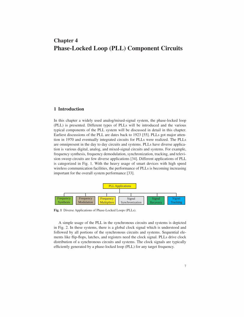
Chapter 4Phase-Locked Loop (PLL) Component Circuits
1 Introduction
In this chapter a widely used analog/mixed-signal system, the phase-locked loop
(PLL) is presented. Different types of PLLs will be introduced and the various
typical components of the PLL system will be discussed in detail in this chapter.
Earliest discussions of the PLL are dates back to 1923 [55]. PLLs got major atten-
tion in 1970 and eventually integrated circuits for PLLs were realized. The PLLs
are omnipresent in the day to day circuits and systems. PLLs have diverse applica-
tion is various digital, analog, and mixed-signal circuits and systems. For example,
frequency synthesis, frequency demodulation, synchronization, tracking, and televi-
sion sweep circuits are few diverse applications [34]. Different applications of PLL
is categorized in Fig. 1. With the heavy usage of smart devices with high speed
wireless communication facilities, the performance of PLLs is becoming increasing
important for the overall system performance [33].
PLL Applications
FrequencySynthesis
FrequencyModulation
FrequencyMultipliers
SignalSynchronization
SignalRecovery
SignalTracking
Fig. 1 Diverse Applications of Phase-Locked Loops (PLLs).
A simple usage of the PLL in the synchronous circuits and systems is depicted
in Fig. 2. In these systems, there is a global clock signal which is understood and
followed by all portions of the synchronous circuits and systems. Sequential ele-
ments like flip-flops, latches, and registers need the clock signal. PLLs drive clock
distribution of a synchronous circuits and systems. The clock signals are typically
efficiently generated by a phase-locked loop (PLL) for any target frequency.
7
79
References
1. All Digital Phase-Locked Loop (ADPLL). http://www.altera.com/products/ip/altera/t-alt-adpll.html. Accessed on 25 June 2013
2. LC Oscillator. http://www.electronics-tutorials.ws/oscillator/oscillators.html. Accessed on 18 June 2013
3. Using Eye Diagrams. http://na.tm.agilent.com/plts/help/WebHelp/Analyzing/Analyzing_Data_using_Eye_Diagrams.html. Accessed on 13June 2013
4. Wolfson Frequency Locked Loop (FLL). http://www.wolfsonmicro.com/documents/uploads/misc/en/WAN0209.pdf (2009). Accessed on 25 June 2013
5. Special Issue on Memristors: Theory and Applications (2013). DOI 10.1109/MCAS.2013.2256252
6. Abidi, A.A.: Phase Noise and Jitter in CMOS Ring Oscillators. IEEE Journal of Solid-StateCircuits 41(8), 1803–1816 (2006). DOI 10.1109/JSSC.2006.876206
7. Aktas, A., Ismail, M.: CMOS PLLs and VCOs for 4G Wireless. Kluwer Academic Publish-ers, Norwell, MA, USA (2004)
8. Apostolidou, M., Baltus, P.G.M., Vaucher, C.S.: Phase Noise In Frequency Divider Circuits.In: Circuits and Systems, 2008. ISCAS 2008. IEEE International Symposium on, pp. 2538–2541 (2008). DOI 10.1109/ISCAS.2008.4541973
9. Appenzeller, J.: Carbon Nanotubes for High-Performance Electronics : Progress andProspect. Proceedings of the IEEE 96(2), 201–211 (2008). DOI 10.1109/JPROC.2007.911051
10. Azais, F., Ivanov, A., Renovell, M., Bertrand, Y.: A Methodology and Design for EffectiveTesting of Voltage Controlled Oscillators (VCOs). In: Proceedings of the Seventh Asian TestSymposium, pp. 383–387 (1998)
11. Baker, R.J.: CMOS Circuit Design, Layout and Simulation, 2 edn. Wiley-IEEE (2008)12. Banerjee, D.: PLL Fundamentals – Part 1: PLL Building Blocks. http://sva.ti.com/
assets/en/other/National_PLL_Building_Blocks.pdf (2009). Accessedon 12 June 2013
13. Best, R.E.: Phase-Locked Loops: Design, Simulation and Applications. McGraw Hill (2007)14. Brennan, P.V., Jiang, D., Wang, H.: Memory-Controlled Frequency Divider For Fractional-N
Synthesisers. Electronics Letters 42(21), 1202–1203 (2006)15. Bunch, R.L., Raman, S.: Large-Signal Analysis of MOS Varactors in CMOS−Gm LC VCOs.
IEEE Journal of Solid-State Circuits 38(8), 1325–1332 (2003). DOI 10.1109/JSSC.2003.814416
16. Casaleiro, J., Lopes, H., Oliveira, L.B., Fernandes, J.R., Silva, M.M.: A 1 mW Low Phase-Noise Relaxation Oscillator. In: Proceedings of the IEEE International Symposium on Cir-cuits and Systems (ISCAS), pp. 1133–1136 (2011). DOI 10.1109/ISCAS.2011.5937770
17. Chaudhuri, S., Jha, N.K.: 3D vs. 2D Analysis of FinFET Logic Gates Under Process Varia-tions. In: Proceedings of the 29th International Conference on Computer Design, pp. 435–436 (2011)
18. Chaudhuri, S., Mishra, P., Jha, N.K.: Accurate Leakage Estimation for FinFET StandardCells Using the Response Surface Methodology. In: Proceedings of the 25th InternationalConference on VLSI Design, pp. 238–244 (2012)
19. Chen, Z., Appenzeller, J., Lin, Y.M., Sippel-Oakley, J., Rinzler, A.G., Tang, J., Wind, S.J.,Solomon, P.M., Avouris, P.: An Integrated Logic Circuit Assembled on a Single CarbonNanotube. Science 311(5768), 1735–1735 (2006)
20. Chen, Z., Appenzeller, J., Solomon, P.M., Lin, Y.M., Avouris, P.: High Performance CarbonNanotube Ring Oscillator. In: Proceedings of the 64th Device Research Conference, pp.171–172 (2006). DOI 10.1109/DRC.2006.305170
21. Cheng, S., Tong, H., Silva-Martinez, J., Karsilayan, A.I.: A Fully Differential Low-PowerDivide-by-8 Injection-Locked Frequency Divider Up to 18 GHz. IEEE Journal of Solid-State Circuits 42(3), 583–591 (2007). DOI 10.1109/JSSC.2006.891448
80
22. Collaert, N., Dixit, A., Goodwin, M., Anil, K.G., Rooyackers, R., Degroote, B., Leunissen,L.H.A., Veloso, A., Jonckheere, R., De Meyer, K., Jurczak, M., Biesemans, S.: A Functional41-Stage Ring Oscillator Using Scaled FinFE Devices With 25-nm Gate Lengths and 10-nmFin Widths Applicable for the 45-Nm CMOS Node. IEEE Electron Device Letters 25(8),568–570 (2004). DOI 10.1109/LED.2004.831585
23. Corinto, F., Ascoli, A., Gilli, M.: Nonlinear Dynamics of Memristor Oscillators. IEEETransactions on Circuits and Systems I: Regular Papers 58(6), 1323–1336 (2011). DOI10.1109/TCSI.2010.2097731
24. Demir, A., Mehrotra, A., Roychowdhury, J.: Phase noise in oscillators: a unifying theory andnumerical methods for characterization. Circuits and Systems I: Fundamental Theory andApplications, IEEE Transactions on 47(5), 655–674 (2000). DOI 10.1109/81.847872
25. Denier, U.: Analysis and Design of an Ultralow-Power CMOS Relaxation Oscillator. IEEETransactions on Circuits and Systems I: Regular Papers 57(8), 1973–1982 (2010). DOI10.1109/TCSI.2010.2041504
26. Deo, S., Menon, S., Nallathambhi, S., Soderstrand, M.A.: Improved Numerically-ControlledDigital Sinusoidal Oscillator. In: Proceedings of the IEEE 45th Midwest Symposium on Cir-cuits and Systems, vol. 2, pp. II–211–II–214 (2002). DOI 10.1109/MWSCAS.2002.1186835
27. Eken, Y.A.: High Frequency Voltage Controlled Oscillators in Standard CMOS. Ph.D. thesis,School of Electrical and Computer Engineering, Georgia Institute of Technology, GA, USA(2003). Accessed on 11 June 2013
28. Elwakil, A.S., Murtada, M.A.: All Possible Canonical Second-Order Three-ImpedanceClass-A and Class-B Oscillators. Electronics Letters 46(11), 748–749 (2010). DOI10.1049/el.2010.0082
29. Fei, W., Yu, H., Zhang, W., Yeo, K.S.: Design Exploration of Hybrid CMOS and MemristorCircuit by New Modified Nodal Analysis. IEEE Transactions on Very Large Scale Integration(VLSI) Systems 20(6), 1012–1025 (2011). DOI 10.1109/TVLSI.2011.2136443
30. Fischette, D.: First Time, Every Time Practical Tips for Phase-Locked Loop Design. http://www.delroy.com/PLL_dir/tutorial/PLL_tutorial_slides.pdf(2009). Accessed on 10 June 2013
31. Fouda, M.E., Khatib, M.A., Mosad, A.G., Radwan, A.G.: Generalized analysis of symmetricand asymmetric memristive two-gate relaxation oscillators. IEEE Transactions on Circuitsand Systems I: Regular Papers p. in press (2013). DOI 10.1109/TCSI.2013.2249172
32. Frederic, C., Gilles, J.: Tutorial 1 : Fundamentals About PLL. http://www.same-conference.org/same_2008/images/documents/SLIDE/TECHNICAL/Tutorial_1_TI_Polytech.pdf (2008). Accessed on 09 June 2013
33. Galton, I., Razavi, B., Cowles, J., Kinget, P.: CMOS Phase-Locked Loops for FrequencySynthesis. In: Proceedings of the IEEE International Solid-State Circuits Conference Digestof Technical Papers (ISSCC), pp. 521–521 (2010). DOI 10.1109/ISSCC.2010.5433853
34. Garitselov, O.: Metamodeling-Based Fast Optimization Of Nanoscale AMS-SoCs. Ph.D.thesis, Computer Science and Engineering, University Of North Texas, Denton, TX, Denton,TX 76207 (2012)
35. Garitselov, O., Mohanty, S.P., Kougianos, E.: A Comparative Study of Metamodels for Fastand Accurate Simulation of Nano-CMOS Circuits. IEEE Transactions on SemiconductorManufacturing 25(1), 26–36 (2012)
36. Garitselov, O., Mohanty, S.P., Kougianos, E.: Accurate Polynomial Metamodeling-BasedUltra-Fast Bee Colony Optimization of a Nano-CMOS PLL. ASP Journal of Low PowerElectronics 8(3), 317–328 (2012)
37. Garitselov, O., Mohanty, S.P., Kougianos, E., Okobiah, O.: Metamodel-Assisted Ultra-FastMemetic Optimization of a PLL for WiMax and MMDS Applications. In: Proceedings ofthe 13th International Symposium on Quality Electronic Design, pp. 580–585 (2012)
38. Gates, E.: Introduction to Electronics. Delmar Cengage Learning, Clifton Park, NY 12065(2011). URL http://books.google.com/books?id=JS\_c1ttnwn8C
39. Ghai, D.: Variability Aware Low-Power Techniques for Nanoscale Mixed-Signal Circuits.Ph.D. thesis, Department of Computer Science and Engineering, University of North Texas,Denton (2009)
81
40. Ghai, D., Mohanty, S.P., Kougianos, E.: Parasitic Aware Process Variation Tolerant VoltageControlled Oscillator (VCO) Design. In: Proceedings of the 9th International Symposium onQuality of Electronic Design, pp. 330–333 (2008)
41. Ghai, D., Mohanty, S.P., Kougianos, E.: Design of Parasitic and Process-Variation AwareNano-CMOS RF Circuits: A VCO Case Study. IEEE Trans. VLSI Syst. 17(9), 1339–1342(2009)
42. Ghai, D., Mohanty, S.P., Kougianos, E.: Unified P4 (power-performance-process-parasitic)fast optimization of a Nano-CMOS VCO. In: Proceedings of the 19th ACM Great Lakessymposium on VLSI, pp. 303–308. ACM (2009)
43. Ghai, D., Mohanty, S.P., Thakral, G.: Comparative Analysis of Double Gate FinFET Config-urations for Analog Circuit Design. In: Proceedings of the IEEE 56th International MidwestSymposium on Circuits and Systems (MWSCAS), p. in press (2013)
44. Ghai, D., Mohanty, S.P., Thakral, G.: Double Gate FinFET based Mixed-Signal Design: AVCO Case Study. In: Proceedings of the IEEE 56th International Midwest Symposium onCircuits and Systems (MWSCAS), p. in press (2013)
45. Ghai, D., Mohanty, S.P., Thakral, G.: Fast Analog Design Optimization Using Regression-Based Modeling and Genetic Algorithm: A Nano-CMOS VCO Case Study. In: Proceedingsof the International Symposium on Quality Electronic Design, pp. 406–411 (2013)
46. Ghai, D., Mohanty, S.P., Thakral, G.: Fast Optimization Of Nano-CMOS Voltage-ControlledOscillator Using Polynomial Regression and Genetic Algorithm. Microelectronics Journal(0), in press (2013). DOI http://dx.doi.org/10.1016/j.mejo.2013.04.010. URL http://www.sciencedirect.com/science/article/pii/S0026269213001067
47. Ghidini, C., Aranda, J.G., Gerna, D., Kelliher, K., Baumhof, C.: A Digitally ProgrammableOn-Chip RC-Oscillator In 0.25μm CMOS Logic Process. In: Proceedings of the IEEEInternational Symposium on Circuits and Systems, pp. 400–403 Vol. 1 (2005). DOI10.1109/ISCAS.2005.1464609
48. Gupta, S.C.: Phase-Locked Loops. Proceedings of the IEEE 63(2), 291–306 (1975)49. H. Lee and T. Choi and S. Mohammadi and L. P. B. Katehi: An Extremely Low Power 2 GHz
CMOS LC VCO for Wireless Communication Applications. In: Proceedings of the EuropeanConference on Wireless Technology, pp. 31–34 (2005). DOI 10.1109/ECWT.2005.1617647
50. Hajimiri, A., Limotyrakis, S., Lee, T.H.: Jitter and Phase Noise in Ring Oscillators. IEEEJournal of Solid-State Circuits 34(6), 790–804 (1999). DOI 10.1109/4.766813
51. Ham, D., Hajimiri, A.: Concepts and Methods in Optimization of Integrated LC VCOs. IEEEJournal of Solid-State Circuits 36(6), 896–909 (2001). DOI 10.1109/4.924852
52. Hancock, J.: JitterUnderstanding it, Measuring It, Eliminating It Part 1: Jitter Funda-mentals. http://www.highfrequencyelectronics.com/Archives/Apr04/HFE0404_Hancock.pdf (2004). Accessed on 13 June 2013
53. Herzel, F., Razavi, B.: A Study of Oscillator Jitter Due To Supply and Substrate Noise. IEEETransactions on Circuits and Systems II: Analog and Digital Signal Processing 46(1), 56–62(1999). DOI 10.1109/82.749085
54. Hosaka, K., Harase, S., Izumiya, S., Adachi, T.: A Cascode Crystal Oscillator Suitable forIntegrated Circuits. In: Proceedings of the IEEE International Frequency Control Symposiumand PDA Exhibition, pp. 610–614 (2002). DOI 10.1109/FREQ.2002.1075954
55. Hsieh, G.C., Hung, J.C.: Phase-Locked Loop Techniques: A Survey. IEEE Transactions onIndustrial Electronics 43(6), 609–615 (1996). DOI 10.1109/41.544547
56. ta Hsieh, M., Sobelman, G.E.: Comparison of LC and Ring VCOs for PLLs in a 90 nm Dig-ital CMOS Process. http://mountains.ece.umn.edu/˜sobelman/papers/mthsieh_isocc06.pdf (2010). Accessed on 10 June 2013
57. Jacquemod, G., Geynet, L., Nicolle, B., de Foucauld, E., Tatinian, W., Vincent, P.: Design andModelling of A Multi-Standard Fractional PLL in CMOS/SOI Technology. MicroelectronicsJournal 39(9), 1130–1139 (2008). DOI 10.1016/j.mejo.2008.01.069. URL http://www.sciencedirect.com/science/article/pii/S0026269208000992
58. Jiang, S., You, F., He, S.: A Wideband Sigma-Delta PLL Based Phase Modulator With Pre-Distortion Filter. In: Proceedings of the International Conference on Microwave and Millime-ter Wave Technology (ICMMT), vol. 4, pp. 1–4 (2012). DOI 10.1109/ICMMT.2012.6230316
82
59. Joeres, S., Kruth, A., Meike, O., Ordu, G., Sappok, S., Wunderlich, R., Heinen, S.: Designof a Ring-Oscillator with a Wide Tuning Range in 0.13μm CMOS for the use in GlobalNavigation Satellite Systems. In: Proceedings of the Annual Workshop on Circuits, Systemsand Signal Processing (ProRISC), pp. 529–535 (2004)
60. Jung, Y.J., Lee, S.W., Shim, D., Kim, W., Kim, C., Cho, S.I.: A Dual-Loop Delay-LockedLoop Using Multiple Voltage-Controlled Delay Lines. IEEE Journal of Solid-State Circuits36(5), 784–791 (2001). DOI 10.1109/4.918916
61. Kadam, S., Sasidaran, D., Awawdeh, A., Johnson, L., Soderstrand, M.: Comparison of Vari-ous Numerically Controlled Oscillators. In: Proceedings of the IEEE 45th Midwest Sympo-sium on Circuits and Systems, vol. 3, pp. III–200–III–202 (2002). DOI 10.1109/MWSCAS.2002.1187005
62. Kang, J.K., Kim, D.H.: A CMOS Clock and Data Recovery With Two-XOR Phase-Frequency Detector Circuit. In: Proceedings of the IEEE International Symposium on Cir-cuits and Systems, vol. 4, pp. 266–269 (2001). DOI 10.1109/ISCAS.2001.922223
63. Kang, S., Leblebici, Y.: CMOS Digital Inegrated Circuits, 3rd edn. McGraw Hill, New York(2003)
64. Kaya, S., Kulkarni, A.: A Novel Voltage-Controlled Ring Oscillator Based On NanoscaleDG-MOSFETs. In: Proceedings of International Conference on Microelectronics, pp. 417–420 (2008). DOI 10.1109/ICM.2008.5393792
65. Kim, J.H., Kwak, Y.H., Kim, M., Kim, S.W., Kim, C.: A 120-MHz–1.8-GHz CMOS DLL-Based Clock Generator for Dynamic Frequency Scaling. IEEE Journal of Solid-State Circuits41(9), 2077–2082 (2006). DOI 10.1109/JSSC.2006.880609
66. Kougianos, E., Mohanty, S.P.: Impact of Gate-Oxide Tunneling on Mixed-Signal Design andSimulation of A Nano-CMOS VCO. Microelectronics Journal 40(1), 95–103 (2009)
67. Kranti, A., Armstrong, G.A.: Design and Optimization of FinFETs for Ultra-Low-VoltageAnalog Applications. IEEE Transactions on Electron Devices 54(12), 3308–3316 (2007)
68. Lee, T.H., Abshire, P.A.: Design Methodology for a Low-Frequency Current-StarvedVoltage-Controlled Oscillator with a Frequency Divider. In: Proceedings of the IEEE 55th In-ternational Midwest Symposium on Circuits and Systems (MWSCAS), pp. 646–649 (2012).DOI 10.1109/MWSCAS.2012.6292103
69. Leeson, D.B.: A simple model of feedback oscillator noise spectrum. Proceedings of theIEEE 54(2), 329–330 (1966). DOI 10.1109/PROC.1966.4682
70. Li, W., Meiners, J.: Introduction to Phase-Locked Loop System Modeling. TI Analog Appli-cations Journal SLYT015, 198–212 (2000)
71. Loke, A.L.S., Barnes, R.K., Wee, T.T., Oshima, M.M., Moore, C.E., Kennedy, R.R., Gilsdorf,M.J.: A Versatile 90-nm CMOS Charge-Pump PLL for SerDes Transmitter Clocking. IEEEJournal of Solid-State Circuits 41(8), 1894–1907 (2006). DOI 10.1109/JSSC.2006.875289
72. Mansour, M.M., Mansour, M.M.: On the Design of Low Phase-Noise CMOS LC-tank Os-cillators. In: Proceedings of the International Conference on Microelectronics, pp. 407–412(2008). DOI 10.1109/ICM.2008.5393840
73. Mansuri, M., Liu, D., Yang, C.K.K.: Fast Frequency Acquisition Phase-Frequency Detectorsfor Gsamples/s Phase-Locked Loops. IEEE Journal of Solid-State Circuits 37(10), 1331–1334 (2002). DOI 10.1109/JSSC.2002.803048
74. Mathis, W., Bremer, J.: Modelling and Design Concepts for Electronic Oscillators and itsSynchronization. The Open Cybernetics and Systemics Journal 3, 47–60 (2009). Accessedon 11 June 2013
75. Min, S., Copani, T., Kiaei, S., Bakkaloglu, B.: A 90-nm CMOS 5-GHz Ring-Oscillator PLLWith Delay-Discriminator-Based Active Phase-Noise Cancellation. IEEE Journal of Solid-State Circuits 48(5), 1151–1160 (2013). DOI 10.1109/JSSC.2013.2252515
76. Miyazaki, T., Hashimoto, M., Onodera, H.: A Performance Comparison Of PLLs For ClockGeneration Using Ring Oscillator VCO And LC Oscillator in A Digital CMOS Process.In: Proceedings of the Asia and South Pacific Design Automation Conference, pp. 545–546(2004). DOI 10.1109/ASPDAC.2004.1337641
77. Mohanty, S.P.: Memristor: From Basics to Deployment. IEEE Potentials 32(3), 34–39(2013). DOI 10.1109/MPOT.2012.2216298

83
78. Mohanty, S.P., Kougianos, E., Garitselov, O., Molina, J.M.: Polynomial-Metamodel AssistedFast Power Optimization of Nano-CMOS PLL Components. In: Proceeding of the Forum onSpecification and Design Languages, pp. 233–238 (2012)
79. Nonis, R., Da Dalt, N., Palestri, P., Selmi, L.: Modeling, Design and Characterization of ANew Low-Jitter Analog Dual Tuning LC-VCO PLL Architecture. IEEE Journal of Solid-State Circuits 40(6), 1303–1309 (2005). DOI 10.1109/JSSC.2005.848037
80. Nowak, E.J., Ludwig, T., Aller, I., Kedzierski, J., Leong, M., Rainey, B., Breitwisch, M.,Gemhoefer, V., Keinert, J., Fried, D.M.: Scaling Beyond the 65 nm Node with FinFET-DGCMOS. In: Proceedings of the IEEE Custom Integrated Circuits Conference, pp. 339–342(2003). DOI 10.1109/CICC.2003.1249415
81. Palumbo, G., Pappalardo, D.: Charge Pump Circuits: An Overview on Design Strategiesand Topologies. IEEE Circuits and Systems Magazine 10(1), 31–45 (2010). DOI 10.1109/MCAS.2009.935695
82. Perrott, M.H.: Tutorial on Digital Phase-Locked Loops. http://cppsim.org/PLL_Lectures/digital_pll_cicc_tutorial_perrott.pdf (2009). Accessed on18 June 2013
83. Razavi, B.: Design of Millimeter-Wave CMOS Radios: A Tutorial. IEEE Transactions onCircuits and Systems I: Regular Papers 56(1), 4–16 (2009). DOI 10.1109/TCSI.2008.931648
84. Safarian, A.Q., Heydari, P.: A Study of High-Frequency Regenerative Frequency Dividers.In: Proceedings of the IEEE International Symposium on Circuits and Systems, pp. 2695–2698 (2005). DOI 10.1109/ISCAS.2005.1465182
85. Sarivisetti, G.: Design and Optimization of Components in a 45 nm CMOS Phase LockedLoop. Master’s thesis, Computer Science and Engineering, University of North Texas, Den-ton (2006). URL http://books.google.com/books?id=U0m3uAAACAAJ
86. Sheng, D., Chung, C.C., Lee, C.Y.: An All-Digital Phase-Locked Loop with High-Resolutionfor SoC Applications. In: Proceedings of the International Symposium on VLSI Design,Automation and Test, pp. 1–4 (2006). DOI 10.1109/VDAT.2006.258161
87. Solanke, S.V.: Design And Analysis Of Novel Charge Pump Architecture For Phase LockedLoop. Master of technology thesis, National Institute Of Technology, Rourkela, Rourkela,India (2009)
88. Sreeja, B.S., Radha, S.: Optimized 2.4GHz Voltage Controlled Oscillator with a High-QMWCNT Network-Based Pulse-Shaped Inductor. Microelectron. J. 43(1), 1–12 (2012). DOI10.1016/j.mejo.2011.10.005. URL http://dx.doi.org/10.1016/j.mejo.2011.10.005
89. Srivastava, A., Xu, Y., Liu, Y., Sharma, A.K., Mayberry, C.: CMOS LC Voltage ControlledOscillator Design Using Carbon Nanotube Wire Inductors. ACM Journal of Emerging Tech-nologies in Computing Systems 8(3), 15:1–15:9 (2012)
90. Staszewski, R.B., Balsara, P.T.: All-Digital PLL With Ultra Fast Settling. IEEE Transactionson Circuits and Systems II: Express Briefs 54(2), 181–185 (2007). DOI 10.1109/TCSII.2006.886896
91. Sun, W., Li, C., Yu, J.: A Simple Memristor Based Chaotic Oscillator. In: Proceeding of theInternational Conference on Communications, Circuits and Systems, pp. 952–954 (2009).DOI 10.1109/ICCCAS.2009.5250350
92. Tiebout, M.: Low-Power Low-Phase-Noise Differentially Tuned Quadrature VCO Designin Standard CMOS. IEEE Journal of Solid-State Circuits 36(7), 1018–1024 (2001). DOI10.1109/4.933456
93. Wang, Z.: An Analysis of Charge-Pump Phase-Locked Loops. IEEE Transactions on Circuitand Systems-I: Fundamental Theory and Applications 52(10), 2128–2138 (2005)
94. Wu, T., Hanumolu, P.K., Mayaram, K., Moon, U.K.: Method for a Constant Loop Bandwidthin LC-VCO PLL Frequency Synthesizers. IEEE Journal of Solid-State Circuits 44(2), 427–435 (2009). DOI 10.1109/JSSC.2008.2010792
95. Xia, L., Chen, H., Huang, Y., Hong, Z., Chiang, P.: 100-Phase, Dual-Loop Delay-LockedLoop For Impulse Radio Ultra-Wideband Coherent Receiver Synchronisation. IET Circuits,Devices Systems 5(6), 484–493 (2011). DOI 10.1049/iet-cds.2011.0112
84
96. Yang, C.K.K.: Delay-Locked Loops An Overview. Wiley-IEEE Press (2003). Accessed on26 June 2013
97. Yang, R.J., Liu, S.I.: A 2.5 GHz All-Digital Delay-Locked Loop in 0.13 μm CMOSTechnology. IEEE Journal of Solid-State Circuits 42(11), 2338–2347 (2007). DOI10.1109/JSSC.2007.906183
98. Ye, B., Li, T., Han, X., Luo, M.: A Fast-Lock Digital Delay-Locked Loop Controller. In:Proceedings of the 8th IEEE International Conference on ASIC, pp. 809–812 (2009). DOI10.1109/ASICON.2009.5351573
99. Yoon, S.: LC-tank CMOS Voltage-Controlled Oscillators using High Quality Inductors Em-bedded in Advanced Packaging Technologies. Ph.D. thesis, Electrical and Computer Engi-neering, Georgia Institute of Technology, GA, USA (2004)
100. Zhang, X., Apsel, A.B.: A Low-Power, Process-and- Temperature - Compensated Ring Os-cillator With Addition-Based Current Source. IEEE Transactions on Circuits and Systems I:Regular Papers 58(5), 868–878 (2011). DOI 10.1109/TCSI.2010.2092110
101. Zhao, J.: A Low Power CMOS Design of An All Digital Phase Locked Loop. Ph.D. the-sis, Department of Electrical and Computer Engineering, Northeastern University, Boston(2011). Accessed on 28 June 2013
102. Zheng, G., Mohanty, S.P., Kougianos, E., Garitselov, O.: Verilog-AMS-PAM: Verilog-AMSintegrated with Parasitic-Aware Metamodels for Ultra-Fast and Layout-Accurate Mixed-Signal Design Exploration. In: Proceedings of the ACM Great Lakes Symposium on VLSI,pp. 351–356 (2012)
103. Zheng, G., Mohanty, S.P., Kougianos, E., Okobiah, O.: Polynomial Metamodel IntegratedVerilog-AMS for Memristor-Based Mixed-Signal System Design. In: Proceedings of theIEEE 56th International Midwest Symposium on Circuits and Systems (MWSCAS), p. inpress (2013)
104. Zhou, Q., Li, L., Chen, G.: An RC Oscillator With Temperature Compensation For Accu-rate Delay Control In Electronic Detonators. In: Proceedings of the IEEE InternationalConference of Electron Devices and Solid-State Circuits, pp. 274–277 (2009). DOI10.1109/EDSSC.2009.5394266
105. Zidan, M.A., Omran, H., Radwan, A.G., Salama, K.N.: Memristor-Based Reactance-LessOscillator. Electronics Letters 47(22), 1220–1221 (2011). DOI 10.1049/el.2011.2700
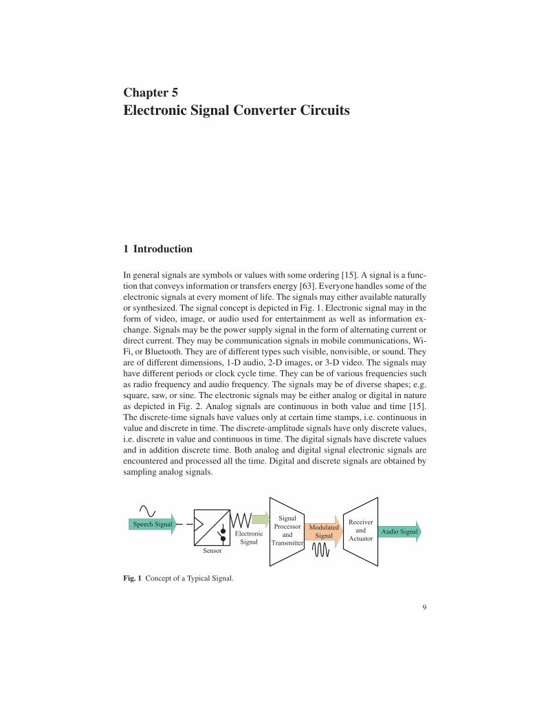
Chapter 5Electronic Signal Converter Circuits
1 Introduction
In general signals are symbols or values with some ordering [15]. A signal is a func-
tion that conveys information or transfers energy [63]. Everyone handles some of the
electronic signals at every moment of life. The signals may either available naturally
or synthesized. The signal concept is depicted in Fig. 1. Electronic signal may in the
form of video, image, or audio used for entertainment as well as information ex-
change. Signals may be the power supply signal in the form of alternating current or
direct current. They may be communication signals in mobile communications, Wi-
Fi, or Bluetooth. They are of different types such visible, nonvisible, or sound. They
are of different dimensions, 1-D audio, 2-D images, or 3-D video. The signals may
have different periods or clock cycle time. They can be of various frequencies such
as radio frequency and audio frequency. The signals may be of diverse shapes; e.g.
square, saw, or sine. The electronic signals may be either analog or digital in nature
as depicted in Fig. 2. Analog signals are continuous in both value and time [15].
The discrete-time signals have values only at certain time stamps, i.e. continuous in
value and discrete in time. The discrete-amplitude signals have only discrete values,
i.e. discrete in value and continuous in time. The digital signals have discrete values
and in addition discrete time. Both analog and digital signal electronic signals are
encountered and processed all the time. Digital and discrete signals are obtained by
sampling analog signals.
Speech Signal
Sensor
Audio SignalElectronicSignal
SignalProcessor
andTransmitter
ModulatedSignal
Receiverand
Actuator
Fig. 1 Concept of a Typical Signal.
9
71
References
1. Defining and Testing Dynamic Parameters in High Speed ADCs, Part 1. http://www.maxim-ic.com/appnotes.cfm/an_pk/728 (2001). Accessed on 02 July 2013
2. INL/DNL Measurements for High-Speed Analog-to-Digital Converters (ADCs). http://www.maximintegrated.com/app-notes/index.mvp/id/283 (2001). Accessedon 15 July 2013
3. Understanding Pipelined ADCs. http://www.maximintegrated.com/app-notes/index.mvp/id/1023 (2001). Accessed on 07 July 2013
4. ADC and DAC Glossary. http://www.maxim-ic.com/app-notes/index.mvp/id/641 (2002). Accessed on 02 July 2013
5. Understanding Integrating ADCs. http://www.maximintegrated.com/app-notes/index.mvp/id/1041 (2002). Accessed on 07 July 2013
6. A Simple ADC Comparison Matrix. http://www.maximintegrated.com/app-notes/index.mvp/id/2094 (2003). Accessed on 10 July 2013
7. Histogram Testing Determines DNL and INL Errors. http://www.maxim-ic.com/appnotes.cfm/an_pk/2085 (2003). Accessed on 02 July 2013
8. RIMs Camera BlackBerry Patent: Not What You Think! (2006). URL http://www.blackberrycool.com/2006/07/07/001980/
9. Electronics Tutorial about Summing Operational Amplifiers. http://www.electronics-tutorials.ws/opamp/opamp_4.html (2013). Accessed on12 July 2013
10. Adams, R., Nguyen, K.Q.: A 113-dB SNR Oversampling DAC With Segmented Noise-ShapedScrambling. IEEE Journal of Solid-State Circuits 33(12), 1871–1878 (1998). DOI 10.1109/4.735526
11. Adeniran, O.., Demosthenous, A., Clifton, C., Atungsiri, S., Soin, R.: A CMOS Low-PowerADC for DVB-T and DVB-H systems. In: Proceedings of the International Symposium onCircuits and Systems, pp. 209–212 (2004)
12. Ahn, S.J., Kim, D.M.: Asynchronous Analogue-to-Digital Converter for Single-Electron Cir-cuits. Electronics Letters 34(2), 172–173 (1998). DOI 10.1049/el:19980157
13. Ale, A.K.: Comparison and Evaluation of Existing Analog Circuit Simulators Using a Sigma-delta Modulator. Master’s thesis, Department of Computer Science and Engineering, Univer-sity of North Texas, Denton (2006). URL http://books.google.com/books?id=c7aouAAACAAJ
14. Allen, P.E., Holberg, D.R.: CMOS Analog Circuit Design, 3rd edn. Oxford University Press,USA (2011)
15. Allen, R.L., Mills, D.: Signal Analysis: Time, Frequency, Scale, and Structure, chap. Signals:Analog, Discrete, and Digital, pp. 1–100. Wiley-IEEE Press, Piscataway, NJ (2004)
16. Anantha, R.R.: A Programmable CMOS Decimator for Sigma Delta Analog-To-Digital Con-verter and Charge Pump Circuits. Master’s thesis, Department of Electrical and ComputerEngineering, Louisiana State University, Baton Rouge, LA (2005). Accessed on 06 July 2013
17. Austerlitz, H.: Data Acquisition Techniques Using PCs. Academic Press, San Diego, CA,USA (2002). URL http://books.google.com/books?id=gK4DxMaqmYYC
18. Aziz, P.M., Sorensen, H.V., vn der Spiegel, J.: An Overview of Sigma-Delta Converters. IEEESignal Processing Magazine 13(1), 61–84 (1996). DOI 10.1109/79.482138
19. Baker, B.: How delta-sigma ADCs work, Part 2. Analog Applications Journal pp. 5–7 (2011).Accessed on 01 August 2013
20. Belega, D., Dallet, D., Petri, D.: Estimation of the Effective Number of Bits of ADCs usingthe Interpolated DFT Method. In: Proceedings of the IEEE Instrumentation and MeasurementTechnology Conference, pp. 30–35 (2010). DOI 10.1109/IMTC.2010.5488200
21. Black, B.: Analog-to-Digital Converter Architectures and Choices for System Design. AnalogDialogue 33(8), 1–4 (1999). Accessed on 03 July 2013
22. Chen, P., Liu, T.C.: Switching Schemes for Reducing Capacitor Mismatch Sensitivity ofQuasi-Passive Cyclic DAC. Circuits and Systems II: Express Briefs, IEEE Transactions on56(1), 26–30 (2009). DOI 10.1109/TCSII.2008.2010158

72
23. Cheung, H., Raj, S.: Implementation of 12-bit Delta-Sigma DAC with MSC12xx Controller.Analog Applications Journal pp. 27–33 (2005)
24. Choudhury, J., Massiha, G.H.: Efficient Encoding Scheme for Ultra-Fast Flash ADC. In: Pro-ceedings of the 5th Topical Meeting on Silicon Monolithic Integrated Circuits in RF Systems,pp. 290–293 (2004)
25. Delagnes, E., Breton, D., Lugiez, F., Rahmanifard, R.: A Low Power Multi-Channel SingleRamp ADC With Up to 3.2 GHz Virtual Clock. IEEE Transactions on Nuclear Science 54(5),1735–1742 (2007). DOI 10.1109/TNS.2007.906170
26. Efstathiou, K.A., Karadimas, D.S.: An R-2R Ladder-Based Architecture for High LinearityDACs. In: Proceedings of the IEEE Instrumentation and Measurement Technology Confer-ence, pp. 1–5 (2007). DOI 10.1109/IMTC.2007.379448
27. Fossum, E.R.: CMOS Image Sensors: Electronic Camera-On-A-Chip. IEEE Transactions onElectron Devices 44(10), 1689–1698 (1997)
28. Fusayasu, T.: A Fast Integrating ADC Using Precise Time-To-Digital Conversion. In: IEEENuclear Science Symposium Conference Record, vol. 1, pp. 302–304 (2007). DOI 10.1109/NSSMIC.2007.4436335
29. Ghai, D.: Variability Aware Low-Power Techniques for Nanoscale Mixed-Signal Circuits.Ph.D. thesis, Department of Computer Science and Engineering, University of North Texas,Denton (2009)
30. Ghai, D., Mohanty, S.P., Kougianos, E.: A 45nm Flash Analog to Digital Converter for LowVoltage High Speed System on Chips. In: Proceedings of the 13th NASA Symposium onVLSI Design, p. 3.1 (2007)
31. Ghai, D., Mohanty, S.P., Kougianos, E.: A Process and Supply Variation Tolerant Nano-CMOSLow Voltage, High Speed, A/D Converter for System-on-Chip. In: Proceedings of the GreatLakes Symposium on VLSI, pp. 47–52 (2008)
32. Ghai, D., Mohanty, S.P., Kougianos, E.: A Variability Tolerant System-on-Chip Ready Nano-CMOS Analog-to-Digital Converter (ADC). Taylor & Francis International Journal of Elec-tronics (IJE) 97(4), 421–440 (2010)
33. Halim, I.S.A., Hassan, S.L.M., Akbar, N.D.B.M., Rahim, A.A.A.: Comparative Study of Com-parator and Encoder in a 4-it Flash ADC Using 0.18μ CMOS Technology. In: Proceedingsof the IEEE Symposium on Computer Applications and Industrial Electronics (ISCAIE), pp.35–38 (2012). DOI 10.1109/ISCAIE.2012.6482064
34. Heij, C.P., Hadley, P., Mooij, J.E.: Single-Electron Inverter. Applied Physics Letters 78(8),1140–1142 (2001). DOI 10.1063/1.1345822. URL http://link.aip.org/link/?APL/78/1140/1
35. Hongqin, L., Xiumin, S.: 18 bit Delta-Sigma DAC in 0.18μm CMOS Process. In: Proceedingsof the 2nd International Conference on Information Science and Engineering (ICISE), pp.3376–3379 (2010). DOI 10.1109/ICISE.2010.5691093
36. Horsky, P.: A 16 Bit+Sign Monotonic Precise Current DAC For Sensor Applications. In:Proceedings of the Design, Automation and Test in Europe Conference and Exhibition, vol. 3,pp. 34–38 (2004). DOI 10.1109/DATE.2004.1269195
37. Huang, C.C., Wang, C.Y., Wu, J.T.: A CMOS 6-Bit 16-GS/s Time-Interleaved ADC UsingDigital Background Calibration Techniques. IEEE Journal of Solid-State Circuits 46(4), 848–858 (2011). DOI 10.1109/JSSC.2011.2109511
38. Jiang, H., Olleta, B., Chen, D., Geiger, R.: A Segmented Thermometer Coded DAC WithDeterministic Dynamic Element Matching For High Resolution ADC Test. In: Circuits andSystems, 2005. ISCAS 2005. IEEE International Symposium on, pp. 784–787 (2005). DOI10.1109/ISCAS.2005.1464705
39. Julsereewong, A., Pongswatd, S., Riewruja, V., Sasaki, H., Fujimoto, K., Shi, Y.: AccurateDual Slope Analog-to-Digital Converter Using Bootstrap Circuit. In: Proceedings of theFourth International Conference on Innovative Computing, Information and Control (ICICIC),pp. 1361–1364 (2009). DOI 10.1109/ICICIC.2009.65
40. Kamath, A.S., Chattopadhyay, B.: A Wide Output Range, Mismatch Tolerant Sigma DeltaDAC for Digital PLL in 90nm CMOS. In: Proceedings of the IEEE International Symposiumon Circuits and Systems, pp. 69–72 (2012). DOI 10.1109/ISCAS.2012.6272127
73
41. Kester, W. (ed.): Analog-Digital Conversion. Analog Devices, Inc. (2004)42. Kester, W.: Understand SINAD, ENOB, SNR, THD, THD + N, and SFDR so You Don’t Get
Lost in the Noise Floor. http://www.analog.com/static/imported-files/tutorials/MT-003.pdf (2009). Accessed on 15 July 2013
43. Kiziroglou, M.E., Karafyllidis, I.: Design And Simulation Of A Nanoelectronic Single-Electron Analog To Digital Converter. Microelectronics Journal 34(9), 785–789 (2003).DOI 10.1016/S0026-2692(03)00153-8. URL http://www.sciencedirect.com/science/article/pii/S0026269203001538
44. Kosonocky, S., Xiao, P.: Digital Signal Processing Handbook, chap. Analog-to-Digital Con-version Architectures, pp. 5.1–5.9. CRC Press LLC, Boca Raton, FL (1997)
45. Lad, K., Bhat, M.S.: A 1-V 1-GS/s 6-bit Low-Power Flash ADC in 90-nm CMOS with 15.75mW Power Consumption. In: Proceedings of the International Conference on Computer Com-munication and Informatics (ICCCI), pp. 1–4 (2013). DOI 10.1109/ICCCI.2013.6466320
46. Le, J.Y., Jiang, J.F., Cai, Q.Y.: Design of Hybrid SET-CMOS D/A Converter. In: Proceedingsof the 4th International Conference on ASIC, pp. 299–302 (2001). DOI 10.1109/ICASIC.2001.982558
47. Lee, D., Yoo, J., Choi, K.: Design Method and Automation of Comparator Generation forFlash A/D Converter. In: Proceedings of the International Symposium on Quality ElectronicsDesign (ISQED), pp. 138–142 (2002)
48. Leung, B.: Pipelined Multi-Bit Oversampled Digital To Analog Converters With CapacitorAveraging. In: Proceedings of the 34th Midwest Symposium on Circuits and Systems, pp.336–339 (1991). DOI 10.1109/MWSCAS.1991.252212
49. Lewyn, L., Ytterdal, T., Wulff, C., Martin, K.: Analog Circuit Design in Nanoscale CMOSTechnologies. Proceedings of the IEEE 97(10), 1687–1714 (2009). DOI 10.1109/JPROC.2009.2024663
50. Li, J., Zhang, J., Shen, B., Zeng, X., Guo, Y., Tang, T.: A 10bit 30MSPS CMOS A/D Converterfor High Performance Video Applications. In: Proceedings of IEEE European Solid-StateCircuits Conference, pp. 523–526 (2005)
51. Lin, C.W., Lin, S.F.: A BIST scheme for testing DAC. In: Electrical Engineering/Electronics,Computer, Telecommunications and Information Technology (ECTI-CON), 2012 9th Interna-tional Conference on, pp. 1–4 (2012). DOI 10.1109/ECTICon.2012.6254328
52. Lin, S.M., Li, D.U., Chen, W.T.: 1 V 1.25 GS/s 8 mW D/A Converters for MB-OFDM UWBTransceivers. In: Proceedings of the IEEE International Conference on Ultra-Wideband, pp.453–456 (2007). DOI 10.1109/ICUWB.2007.4380987
53. Luo, C., McClellan, J.H.: Compressive Sampling With a Successive Approximation ADCArchitecture. In: Proceedings of the IEEE International Conference on Acoustics, Speech andSignal Processing (ICASSP), pp. 3920–3923 (2011). DOI 10.1109/ICASSP.2011.5947209
54. Maloberti, F.: Data Converters. Springer (2007)55. Marche, D., Savaria, Y.: Modeling R-2R Segmented-Ladder DACs. IEEE Transactions on Cir-
cuits and Systems I: Regular Papers 57(1), 31–43 (2010). DOI 10.1109/TCSI.2009.201939656. MobileReference: Electronics Quick Study Guide for Smartphones and Mobile Devices.
Mobi Study Guides. MobileReference.com (2007). URL http://books.google.com/books?id=AG6H633VIAcC
57. Mohanty, S.P., Vadlamudi, S.T., Kougianos, E.: A Universal Voltage Level Converter forMulti-Vdd Based Low-Power Nano-CMOS Systems-on-Chips (SoCs). In: Proceedings of the13th NASA Symposium on VLSI Design, p. 2.2 (2007)
58. Mortezapour, S., Lee, E.K.F.: A Reconfigurable Pipelined Data Converter. In: Proceedingsof the IEEE International Symposium on Circuits and Systems, vol. 4, pp. 314–317 (2001).DOI 10.1109/ISCAS.2001.922235
59. Okada, S., Matsuda, Y., Yamada, T., Kobayashi, A.: System On a Chip for Digital Still Cam-era. IEEE Transactions on Consumer Electronics 45(3), 1689–1698 (1999)
60. Ozalevli, E., Dinc, H., Lo, H.J., Hasler, P.: Design of A Binary-Weighted Resistor DAC UsingTunable Linearized Floating-Gate CMOS Resistors. In: Proceedings of the IEEE CustomIntegrated Circuits Conference, pp. 149–152 (2006). DOI 10.1109/CICC.2006.320867

74
61. Perry, J.C.: Digital to Analog Converter Design using Single Electron Transistors. Master’sthesis, Computer Engineering, Virginia Polytechnic Institute and State University, Blacksburg,Virginia (2005). Accessed on 03 July 2013
62. Plassche, R.J.V.D.:63. Priemer, R.: Introductory Signal Processing. World Scientific (1991)64. Raiteri, D., van Lieshout, P., van Roermund, A., Cantatore, E.: An Organic VCO-based ADC
for Quasi-Static Signals Achieving 1LSB INL at 6b Resolution. In: Proceedings of the IEEEInternational Solid-State Circuits Conference Digest of Technical Papers (ISSCC), pp. 108–109 (2013). DOI 10.1109/ISSCC.2013.6487658
65. Raiteri, D., Torricelli, F., Cantatore, E., Van Roermund, A.H.M.: A Tunable Transconduc-tor for Analog Amplification and Filtering Based on Double-Gate Organic TFTs. In: Pro-ceedings of the European Solid-State Circuits Conference, pp. 415–418 (2011). DOI10.1109/ESSCIRC.2011.6044995
66. Rathore, T.S., Jain, A.: Abundance of Ladder Digital-to-Analog Converters. IEEE Transac-tions on Instrumentation and Measurement 50(5), 1445–1449 (2001). DOI 10.1109/19.963222
67. de la Rosa, J.M.: Sigma-Delta Modulators: Tutorial Overview, Design Guide, and State-of-the-Art Survey. IEEE Transactions on Circuits and Systems I: Regular Papers 58(1), 1–21(2011). DOI 10.1109/TCSI.2010.2097652
68. Sandler, M.B.: Digital-to-Analogue Conversion Using Pulse Width Modulation. ElectronicsCommunication Engineering Journal 5(6), 339–348 (1993)
69. Sarkar, S., Banerjee, S.: An 8-bit 1.8 V 500 MSPS CMOS Segmented Current Steering DAC.In: Proceedings of the IEEE Computer Society Annual Symposium on VLSI, pp. 268–273(2009). DOI 10.1109/ISVLSI.2009.12
70. Schreier, R., Temes, G.C.:71. Shaber, M.U.: Pipeline DA-converter Design and Implementation. Master’s thesis, Depart-
ment of Electronic, Computers and Software Systems (ECS), School for Information andCommunication Technology (ICT), Royal Institute of Technology (KTH) (2005). Accessedon 13 July 2013
72. Shaker, M.O., Bayoumi, M.A.: A 6-bit 130-MS/s Low-Power Tracking ADC in 90 nm CMOS.In: Proceedings of the 53rd IEEE International Midwest Symposium on Circuits and Systems(MWSCAS), pp. 304–307 (2010). DOI 10.1109/MWSCAS.2010.5548814
73. Shaker, M.O., Gosh, S., Bayoumi, M.A.: A 1-GS/s 6-bit Flash ADC in 90nm CMOS. In:Proceedings of the 52nd IEEE International Midwest Symposium on Circuits and Systems,pp. 144–147 (2009). DOI 10.1109/MWSCAS.2009.5236133
74. Srivastava, A., Anantha, R.R.: A Programmable Oversampling Sigma-Delta Analog-to-DigitalConverter. In: Proceedings of the 48th Midwest Symposium on Circuits and Systems, pp.539–542 (2005). DOI 10.1109/MWSCAS.2005.1594157
75. Stanoeva, M., Popov, A.: Investigation of a Parallel Resistorless ADC. In: Proceedings of theInternational Conference on Computer Systems and Technologies, pp. v.8–1–v.8–5 (2005)
76. Stewart, R.W.: An Overview of Sigma Delta ADCs and DAC Devices. In: IEE Colloquiumon Oversampling and Sigma-Delta Strategies for DSP, pp. 1/1–1/9 (1995). DOI 10.1049/ic:19951371
77. Svensson, C., Andersson, S., Bogner, P.: On the power consumption of analog to digital con-verters. In: Proceedings of the 24th Norchip Conference, pp. 49–52 (2006)
78. Titus, A.H., Gopalan, A.: A Differential Summing Amplifier for Analog VLSI Systems. In:Proceedings of the IEEE International Symposium on Circuits and Systems, vol. 4, pp. IV–57–IV–60 (2002). DOI 10.1109/ISCAS.2002.1010387
79. Tucker, J.R.: Complementary Digital Logic Based on The “Coulomb Blockade”. Journal ofApplied Physics 72(9), 4399–4413 (1992). DOI 10.1063/1.352206
80. van Valburg, J., van de Plassche, R.: An 8b 650MHz Folding ADC. In: Digest of TechnicalPapers 39th IEEE International Solid-State Circuits Conference, pp. 30–31 (1992). DOI10.1109/ISSCC.1992.200395
81. van Valburg, J., van de Plassche, R.J.: An 8-b 650-MHz Folding ADC. IEEE Journal of Solid-State Circuits 27(12), 1662–1666 (1992). DOI 10.1109/4.173091
75
82. Vogel, C.: The impact of combined channel mismatch effects in time-interleaved adcs.Instrumentation and Measurement, IEEE Transactions on 54(1), 415–427 (2005). DOI10.1109/TIM.2004.834046
83. Wang, S., Ahmad, M.O., Bhattacharrya, B.B.: A Novel Cyclic D/A Converter. In: Proceedingsof the IEEE International Symposium on Circuits and Systems, pp. 1224–1227 (1993). DOI10.1109/ISCAS.1993.393949
84. Weaver, S., Hershberg, B., Hanumolu, P.K., Moon, U.K.: A Multiplexer-Based Digital PassiveLinear Counter (PLINCO). In: Proceedings of the 16th IEEE International Conference onElectronics, Circuits, and Systems, pp. 607–610 (2009). DOI 10.1109/ICECS.2009.5410852
85. Wietsma, T.A., Minsker, B.S.: Adaptive Sampling of Streaming Signals. In: Proceedingsof the IEEE 8th International Conference on E-Science (e-Science), pp. 1–7 (2012). DOI10.1109/eScience.2012.6404475
86. Xiong, W., Guo, Y., Zschieschang, U., Klauk, H., Murmann, B.: A 3-V, 6-Bit C-2C Digital-to-Analog Converter Using Complementary Organic Thin-Film Transistors on Glass. IEEEJournal of Solid-State Circuits 45(7), 1380–1388 (2010). DOI 10.1109/JSSC.2010.2048083
87. Xiong, W., Zschieschang, U., Klauk, H., Murmann, B.: A 3V 6b Successive-ApproximationADC using Complementary Organic Thin-Film Transistors on Glass. In: Proceedings of theIEEE International Solid-State Circuits Conference Digest of Technical Papers (ISSCC), pp.134–135 (2010). DOI 10.1109/ISSCC.2010.5434017
88. Yang, J., Wu, X., Zhao, J.: A RC Reconstruction Filter For a 16-bit Audio Delta-Sigma DAC.In: Proceedings of the IEEE 11th International Conference on Solid-State and Integrated Cir-cuit Technology (ICSICT), pp. 1–3 (2012). DOI 10.1109/ICSICT.2012.6467729
89. Yang, Y., Sculley, T., Abraham, J.: A Single-Die 124 dB Stereo Audio Delta-Sigma ADCWith 111 dB THD. IEEE Journal of Solid-State Circuits 43(7), 1657–1665 (2008). DOI10.1109/JSSC.2008.923731
90. Yoo, J., Choi, K., Ghaznavi, J.: A 0.07μm CMOS Flash Analog to Digital Converter for HighSpeed and Low Voltage Applications. In: Proceedings of the Great Lakes Symposium onVLSI, pp. 56–59 (2003)
91. Yoo, J., Choi, K., Tangel, A.: A 1-GSPS CMOS Flash A/D Converter for System-on-ChipApplications. In: Proceedings of the IEEE Computer Society Workshop on VLSI, pp. 135–139 (2001)
92. Yuan, J., Fung, S.W., Chan, K.Y., Xu, R.: An Interpolation-Based Calibration Architecture forPipeline ADC With Nonlinear Error. IEEE Transactions on Instrumentation and Measurement61(1), 17–25 (2012). DOI 10.1109/TIM.2011.2161026
93. Yuan, J., Svensson, C.: A 10-bit 5-MS/s Successive Approximation ADC Cell used in a 70-MS/s ADC Array in 1.2-μm CMOS. IEEE Journal of Solid-State Circuits 29(8), 866–872(1994). DOI 10.1109/4.297689
94. Zheng, G., Mohanty, S.P., Kougianos, E.: Design and Modeling of A Continuous-Time Delta-Sigma Modulator For Biopotential Signal Acquisition: Simulink Vs. Verilog-AMS Perspec-tive. In: Proceedings of the Third International Conference on Computing CommunicationNetworking Technologies (ICCCNT), pp. 1–6 (2012). DOI 10.1109/ICCCNT.2012.6396103
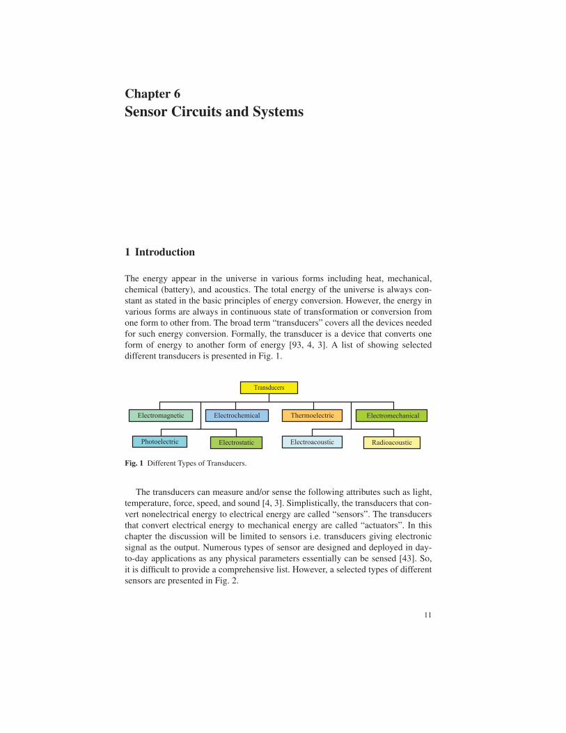
Chapter 6Sensor Circuits and Systems
1 Introduction
The energy appear in the universe in various forms including heat, mechanical,
chemical (battery), and acoustics. The total energy of the universe is always con-
stant as stated in the basic principles of energy conversion. However, the energy in
various forms are always in continuous state of transformation or conversion from
one form to other from. The broad term “transducers” covers all the devices needed
for such energy conversion. Formally, the transducer is a device that converts one
form of energy to another form of energy [93, 4, 3]. A list of showing selected
different transducers is presented in Fig. 1.
Transducers
ElectromechanicalElectromagnetic Electrochemical
ElectroacousticPhotoelectric Electrostatic
Thermoelectric
Radioacoustic
Fig. 1 Different Types of Transducers.
The transducers can measure and/or sense the following attributes such as light,
temperature, force, speed, and sound [4, 3]. Simplistically, the transducers that con-
vert nonelectrical energy to electrical energy are called “sensors”. The transducers
that convert electrical energy to mechanical energy are called “actuators”. In this
chapter the discussion will be limited to sensors i.e. transducers giving electronic
signal as the output. Numerous types of sensor are designed and deployed in day-
to-day applications as any physical parameters essentially can be sensed [43]. So,
it is difficult to provide a comprehensive list. However, a selected types of different
sensors are presented in Fig. 2.
11
73
References
1. A Short Course in Digital Photography: Chapter 2 The Foundations of Digital Imag-ing. http://btc.montana.edu/ceres/malcolm/cd/universe/assets/multimedia/chapter02.pdf. Accessed on 26 Aug 2013
2. CMOS Fundamentals. http://www.siliconimaging.com/cmos_fundamentals.htm. Accessed on 26 Aug 2013
3. Instrumentation-Electronics. http://www.instrumentationtoday.com/4. Sensors and Transducers. http://www.electronics-tutorials.ws/io/io_1.
html. Accessed on 05 Aug 20135. Solar Electricity Basics. http://homepower.com/basics/solar/ (2012). Ac-
cessed on 19 August 20136. Alem, S., de Bettignies, R., Nunzi, J.M., Cariou, M.: Efficient Polymer-Based Interpen-
etrated Network Photovoltaic Cells, publisher = AIP, year = 2004, journal = AppliedPhysics Letters, volume = 84, number = 12, pages = 2178–2180, keywords = filledpolymers; conducting polymers; solar cells; surface treatment; surface morphology, url =http://link.aip.org/link/?APL/84/2178/1, doi = 10.1063/1.1669065
7. Almazan, S.P.R., Zarsuela, J.V., Alarcon, A.P.B.L.P.: A Study on the Effect of Varying Volt-age Supply on the Performance of Voltage Sense Amplifiers for 1-Transistor DRAM Mem-ories. In: Proceedings of the IEEE International Conference on Semiconductor Electronics,pp. 108–112 (2008)
8. Almazan, S.P.R., Zarsuela, J.V., Ballesil, A.P., Alarcon, L.P.: A Study on The Effect of Vary-ing Voltage Supply on The Performance of Voltage Sense Amplifiers For 1-Transistor DRAMMemories. In: Proceedings of the IEEE International Conference on Semiconductor Elec-tronics, pp. 108–112 (2008). DOI 10.1109/SMELEC.2008.4770287
9. Amrutur, B.S.: Design And Analysis of Fast Low Power SRAMs. Dissertation, ElectricalEngineering, Stanford University (1999). Accessed on 06 Sep 2013
10. Artyomov, E., Yadid-Pecht, O.: Adaptive Multiple-Resolution CMOS Active Pixel Sensor.IEEE Transactions on Circuits and Systems 53(10), 2178–2186 (2006)
11. Atashbar, M., Bejcek, B., Singamaneni, S., Santucci, S.: Carbon Nanotube Based Biosen-sors. In: Proceedings of IEEE Sensors, pp. 1048–1051 (2004). DOI 10.1109/ICSENS.2004.1426354
12. Bi, X., Zhang, C., Li, H., Chen, Y., Pino, R.: Spintronic Memristor Based Temperature SensorDesign With CMOS Current Reference. In: Proceedings of the Design, Automation Test inEurope Conference Exhibition (DATE), pp. 1301–1306 (2012). DOI 10.1109/DATE.2012.6176693
13. Bohndiek, S.E., Blue, A., Clark, A., Prydderch, M., Turchetta, R., Royle, G., Speller, R.:Comparison of methods for estimating the conversion gain of cmos active pixel sensors.Sensors Journal, IEEE 8(10), 1734–1744 (2008). DOI 10.1109/JSEN.2008.2004296
14. Casadei, B., Hu, Y., Dufaza, C., Martin, L.: Model for Electrical Simulation of Photogate Ac-tive Pixel Sensor. In: Proceedings of the 16th International Conference on Microelectronics,pp. 189–193 (2004)
15. Chamberlain, S.G., Lee, J.P.Y.: A Novel Wide Dynamic Range Silicon Photodetector andLinear Imaging Array. IEEE Transactions on Electron Devices 31(2), 175–182 (1984). DOI10.1109/T-ED.1984.21498
16. Chapman, G., Audet, Y.: Creating 35 mm Camera Active Pixel Sensors. In: Proceedingsof the International Symposium on Defect and Fault Tolerance in VLSI Systems, pp. 22–30(1999). DOI 10.1109/DFTVS.1999.802865
17. Cheknane, A., Hilal, H.S., Djeffal, F., Benyoucef, B., Charles, J.P.: An Equivalent CircuitApproach To Organic Solar Cell Modelling. Microelectronics Journal 39(10), 1173–1180(2008). DOI http://dx.doi.org/10.1016/j.mejo.2008.01.053
18. Chen, P., Chen, C.C., Tsai, C.C., Lu, W.F.: A Time-to-Digital-Converter-Based CMOS SmartTemperature Sensor. Solid-State Circuits, IEEE Journal of 40(8), 1642– 1648 (2005)
74
19. Chen, S., Tang, W., Culurciello, E.: A 64×64 Pixels UWB Wireless Temporal-DifferenceDigital Image Sensor. In: Proceedings of IEEE International Symposium on Circuits andSystems (ISCAS), pp. 1404–1407 (2010). DOI 10.1109/ISCAS.2010.5537283
20. Chen, S., Tang, W., Zhang, X., Culurciello, E.: A 64×64 Pixels UWB Wireless Temporal-Difference Digital Image Sensor. IEEE Transactions on Very Large Scale Integration (VLSI)Systems 20(12), 2232–2240 (2012). DOI 10.1109/TVLSI.2011.2172470
21. Chen, T., Catrysse, P.B., El Gamal, A., Wandell, B.A.: How Small Should Pixel Size Be?(2000). DOI 10.1117/12.385463. URL http://dx.doi.org/10.1117/12.385463
22. Chen, Y., Wang, X., Sun, Z., Li, H.: The Application of Spintronic Devices in MagneticBio-Sensing. In: Proceedings of the 2nd Asia Symposium on Quality Electronic Design(ASQED), pp. 230–234 (2010). DOI 10.1109/ASQED.2010.5548244
23. Chin, M., Kilpatrick, S.: Differential Amplifier Circuits Based on Carbon Nanotube Field Ef-fect Transistors (CNTFETs). Tech. Rep. ARL-TR-5151, Army Research Laboratory (2010).Accessed on 10 Aug 2013
24. Cho, T.S.: An Energy Efficient CMOS Interface to Carbon Nanotube Sensor Arrays. Master’sthesis, Department of Electrical Engineering and Computer Science, Massachusetts Instituteof Technology, Cambridge, MA (2007). Accessed on 10 Aug 2013
25. Cho, T.S., Lee, K.J., Kong, J., Chandrakasan, A.: A Low Power Carbon Nanotube ChemicalSensor System. In: Proceedings of the IEEE Custom Integrated Circuits Conference, pp.181–184 (2007). DOI 10.1109/CICC.2007.4405708
26. Cho, T.S., Lee, K.J., Kong, J., Chandrakasan, A.P.: The Design of A Low Power Carbon Nan-otube Chemical Sensor System. In: Proceedings of the 45th ACM/IEEE Design AutomationConference, pp. 84–89 (2008)
27. Choppali, U., Kougianos, E., Mohanty, S.P., Gorman, B.P.: Polymeric precursor de-rived nanocrystalline zno thin films using {EDTA} as chelating agent. Solar En-ergy Materials and Solar Cells 94(12), 2351 – 2357 (2010). DOI http://dx.doi.org/10.1016/j.solmat.2010.08.012. URL http://www.sciencedirect.com/science/article/pii/S0927024810004691
28. Choppali, U., Kougianos, E., Mohanty, S.P., Gorman, B.P.: Maskless Deposition of ZnOFilms. Solar Energy Materials and Solar Cells 95(3), 870–876 (2011). DOI http://dx.doi.org/10.1016/j.solmat.2010.11.004. URL http://www.sciencedirect.com/science/article/pii/S0927024810006471
29. Choudhary, A.: Process Variation Tolerant Self Compensation Sense Amplifier Design. The-sis, University of Massachusetts Amherst (2008)
30. Choudhary, A., Kundu, S.: A Process Variation Tolerant Self-Compensating Sense AmplifierDesign. In: Proceedings of the IEEE Computer Society Annual Symposium on VLSI, pp.263–267 (2009)
31. Chow, H.C., Hsieh, C.L.: A 0.5V High Speed DRAM Charge Transfer Sense Amplifier.In: Proceedings of the 50th Midwest Symposium on Circuits and Systems, pp. 1293–1296(2007)
32. Cirmirakis, D., Demosthenous, A., Saeidi, N., Donaldson, N.: Humidity-to-Frequency Sen-sor in CMOS Technology With Wireless Readout. IEEE Sensors Journal 13(3), 900–908(2013). DOI 10.1109/JSEN.2012.2217376
33. Collins, P.G., Bradley, K., Ishigami, M., Zettl, A.: Extreme Oxygen Sensitivity of Elec-tronic Properties of Carbon Nanotubes. Science 287(5459), 1801–1804 (2000). DOI10.1126/science.287.5459.1801. URL http://www.sciencemag.org/content/287/5459/1801.abstract
34. Datta, B.: On-Chip Thermal Sensing in Deep Sub-Micron CMOS. Master’s thesis, ElectricalAnd Computer Engineering, University of Massachusetts Amherst, Amherst, MA (2007)
35. Datta, B., Burleson, W.: Low-Power and Robust On-Chip Thermal Sensing Using Differ-ential Ring Oscillators. In: Proceedings of the 50th Midwest Symposium on Circuits andSystems, pp. 29–32 (2007). DOI 10.1109/MWSCAS.2007.4488534
36. Davis, B.T.: Modern DRAM Architectures. Dissertation, Computer Science and Engineer-ing, The University of Michigan (2001). Accessed on 06 Sep 2013

75
37. Dutta, A.K.: Prospects of Nanotechnology for High-Efficiency Solar Cells. In: Proceedingsof the 7th International Conference on Electrical Computer Engineering (ICECE), pp. 347–350 (2012). DOI 10.1109/ICECE.2012.6471558
38. Feruglio, S., Hanna, V.F., Alquie, G., Vasilescu, G.: Dark Current and Signal-to-Noise Ra-tio in BDJ Image Sensors. IEEE Transactions on Instrumentation and Measurement 55(6),1892–1903 (2006). DOI 10.1109/TIM.2006.884291
39. Fiori, F., Crovetti, P.S.: A New Compact Temperature-Compensated CMOS Current Refer-ence. Circuits and Systems II: Express Briefs, IEEE Transactions on 52(11), 724–728 (2005).DOI 10.1109/TCSII.2005.852529
40. Fish, A., Yadid-Pecht, O.: Low-Power “Smart” CMOS Image Sensors. In: Proceedings ofthe IEEE International Symposium on Circuits and Systems, pp. 1408–1411 (2008). DOI10.1109/ISCAS.2008.4541691
41. Fossum, E.R.: CMOS Image Sensors: Electronic Camera on a Chip. In: Proceedings ofthe International Electron Devices Meeting, pp. 17–25 (1995). DOI 10.1109/IEDM.1995.497174
42. Fossum, E.R.: CMOS Image Sensors: Electronic Camera on a Chip. IEEE Transactions onElectron Devices 44, 1689–16,984 (1997)
43. Fraden, J.: Handbook of Modern Sensors: Physics, Designs, and Applications. Springer(2010). URL http://books.google.com/books?id=W0Emv9dAJ1kC
44. Fujimori, I.L., Wang, C.C., Sodini, C.G.: A 256 × 256 CMOS Differential Passive PixelImager With FPN Reduction Techniques. In: Proceedings of the IEEE International Solid-State Circuits Conference, pp. 106–107 (2000). DOI 10.1109/ISSCC.2000.839711
45. Galiana, B., Algora, C., Rey-Stolle, I., Vara, I.G.: A 3-D Model For Concentrator Solar CellsBased On Distributed Circuit Units. IEEE Transactions on Electron Devices 52(12), 2552–2558 (2005). DOI 10.1109/TED.2005.859620
46. Gamal, A.E., Eltoukhy, H.: CMOS Image Sensors. IEEE Circuits and Devices Magazine21(3), 6–20 (2005)
47. Garcia, I., Algora, C., Rey-Stolle, I., Galiana, B.: Study of Non-Uniform Light Profiles onHigh Concentration III-V Solar Cells Using Quasi-3D Distributed Models. In: Proceedingsof the 33rd IEEE Photovoltaic Specialists Conference, pp. 1–6 (2008). DOI 10.1109/PVSC.2008.4922908
48. Gautschi, G.: Piezoelectric Sensorics: Force, Strain, Pressure, Acceleration and AcousticEmission Sensors, Materials and Amplifiers. Engineering Online Library. Springer (2002).URL http://books.google.com/books?id=-nYFSLcmc-cC
49. Geib, H., Raab, W., Schmitt-Landsiedel, D.: Block-Decoded Sense-Amplifier Driver forHigh-Speed Sensing in DRAM’s. IEEE Journal of Solid-State Circuits 27(9), 1286–1288(1992)
50. Geib, H., Weber, W., Wohlrab, E., Risch, L.: Experimental Investigation of the MinimumSignal for Reliable Operation of DRAM Sense Amplifiers. IEEE Jounal of Solid-State Cir-cuits 27(7), 1028–1035 (1992)
51. Ghai, D.: Variability Aware Low-Power Techniques for Nanoscale Mixed-Signal Circuits.Ph.D. thesis, Department of Computer Science and Engineering, University of North Texas,Denton (2009)
52. Ghai, D., Mohanty, S.P., Kougianos, E.: Variability-Aware Optimization Of Nano-CMOSActive Pixel Sensors using design and Analysis Of Monte Carlo Experiments. In: Proceed-ings of the 10th International Symposium on Quality of Electronic Design, pp. 172–178(2009)
53. H. Tian B. Fowler, A.G.: Analysis of Temporal Noise in CMOS Photodiode Active PixelSensor. IEEE Journal of Solid-State Circuits 36, 92–101 (2001)
54. Hidaka, Y., Kawahara, K.: Modeling of A Hybrid System of Photovoltaic and Fuel Cell ForOperational Strategy in Residential Use. In: Proceedings of the 47th International Univer-sities Power Engineering Conference (UPEC), pp. 1–6 (2012). DOI 10.1109/UPEC.2012.6398416
76
55. Hong, S., Kim, S., Wee, J.K., Lee, S.: Low-Voltage DRAM Sensing Scheme With Offset-Cancellation Sense Amplifier. IEEE Journal of Solid-State Circuits 37(10), 1356–1360(2002)
56. Hou, K.C., Chang, C.W., Chiou, J.C., Huang, Y.H., Shaw, F.Z.: Wireless and batterylessbiomedical microsystem for neural recording and epilepsy suppression based on brain focalcooling. IET Nanobiotechnology 5(4), 143–147 (2011). DOI 10.1049/iet-nbt.2011.0017
57. I. Shcherback, O.Y.P.: Photoresponse Analysis And Pixel Shape Optimization For Cmos Ac-tive Pixel Sensors. IEEE Transactions on Electron Devices 50, 12–18 (2003)
58. Ignjatovic, Z., Maricic, D., Bocko, M.F.: Low Power, High Dynamic Range CMOS ImageSensor Employing Pixel-Level Oversampling ΣΔ Analog-to-Digital Conversion. SensorsJournal, IEEE 12(4), 737–746 (2012). DOI 10.1109/JSEN.2011.2158818
59. Im, H., Huang, X.J., Gu, B., Choi, Y.K.: A Dielectric-Modulated Field-Effect Transistor ForBiosensing. Nature Nanotechnology 2(7), 430–434 (2007). DOI http://dx.doi.org/10.1038/nnano.2007.180
60. Jiang, T., Chiang, P.Y.: Sense Amplifier Power and Delay Characterization for OperationUnder Low-Vdd and Low-voltage Clock Swing. Proceedings of the IEEE International Sym-posium on Circuits and Systems pp. 181–184 (2009)
61. Jianping, S.: An Optimum Layout Scheme For Photovoltaic Cell Arrays Using PVSYST. In:Proceedings of the International Conference on Mechatronic Science, Electric Engineeringand Computer (MEC), pp. 243–245 (2011). DOI 10.1109/MEC.2011.6025446
62. Khatri, I., Bao, J., Kishi, N., Soga, T.: Similar Device Architectures for Inverted Or-ganic Solar Cell and Laminated Solid-State Dye-Sensitized Solar Cells. ISRN Electronics2012(180787), 1–11 (2012). DOI http://dx.doi.org/10.5402/2012/180787
63. Kim, C.H., Jung, C., Lee, K.B., Park, H.G., Choi, Y.K.: Label-free DNA Detection WithA Nanogap Embedded Complementary Metal Oxide Semiconductor. IOP Nanotechnology22(13), 135,502 (2011). DOI doi:10.1088/0957-4484/22/13/135502
64. Kleinfelder, S., Bieser, F., Chen, Y., Gareus, R., Matis, H.S., Oldenburg, M., Retiere, F.,Ritter, H.G., Wieman, H.H., Yamamoto, E.: Novel Integrated CMOS Sensor Circuits. IEEETransactions on Nuclear Science 51(5), 2328–2336 (2004). DOI 10.1109/TNS.2004.836150
65. Kleinfelder, S., Lim, S., Liu, X., El Gamal, A.: A 10000 Frames/s CMOS Digital Pixel Sen-sor. IEEE Journal of Solid-State Circuits 36(12), 2049–2059 (2001). DOI 10.1109/4.972156
66. Kon, S., Horowitz, R.: A High-Resolution MEMS Piezoelectric Strain Sensor for StructuralVibration Detection. IEEE Sensors Journal 8(12), 2027–2035 (2008). DOI 10.1109/JSEN.2008.2006708
67. Kong, J., Franklin, N.R., Zhou, C., Chapline, M.G., Peng, S., Cho, K., Dai, H.: NanotubeMolecular Wires as Chemical Sensors. Science 287(5453), 622–625 (2000). DOI 10.1126/science.287.5453.622. URL http://www.sciencemag.org/content/287/5453/622.abstract
68. Kuila, T., Bose, S., Khanra, P., Mishra, A.K., Kim, N.H., Lee, J.H.: Recent Advances inGraphene-Based Biosensors. Biosensors and Bioelectronics 26(12), 4637–4648 (2011). DOIhttp://dx.doi.org/10.1016/j.bios.2011.05.039. URL http://www.sciencedirect.com/science/article/pii/S0956566311003368
69. Lee, C.Y., Baik, S., Zhang, J., Masel, R.I., Strano, M.S.: Charge Transfer From Metal-lic Single-Walled Carbon Nanotube Sensor Arrays. The Journal of Physical Chemistry B110(23), 11,055–11,061 (2006). URL http://www.ncbi.nlm.nih.gov/pubmed/16771365
70. Liu, S., Guo, X.: Carbon Nanomaterials Field-Effect-Transistor-Based Biosensors. NPGAsia Materials 4(8), 1–10 (2012). DOI http://dx.doi.org/10.1038/am.2012.42
71. Liu, X.: CMOS Image Sensors Dynamic Range and SNR Enhancement Via Statistical SignalProcessing. Dissertation, Stanford University (2002). Accessed on 26 Aug 2013
72. Ludvig, N., Medveczky, G., French, J.A., Carlson, C., Devinsky, O., Kuzniecky, R.I.: Evolu-tion and Prospects for Intracranial Pharmacotherapy for Refractory Epilepsies: The Subdu-ral Hybrid Neuroprosthesis. Epilepsy Research and Treatment 2010(725696), 1–10 (2009).DOI http://dx.doi.org/10.1155/2010/725696
77
73. Lukac, R., Plataniotis, K.N.: Secure Single-Sensor Digital Camera. Electronics Letters42(11), 627–629 (2006). DOI 10.1049/iel:20060604
74. M. Beiderman, M., Tam, T., Fish, A., Jullien, G.A., Yadid-Pecht, O.: A Low Noise CMOSImage Sensor with an Emission Filter for Fluorescence Applications. In: Proceedings of theInternational Conference on Circuits and Systems, pp. 1100–1103 (2008)
75. Mazhari, B.: An Improved Solar Cell Circuit Model For Organic Solar Cells. Solar En-ergy Materials and Solar Cells 90(7?8), 1021–1033 (2006). DOI http://dx.doi.org/10.1016/j.solmat.2005.05.017. URL http://www.sciencedirect.com/science/article/pii/S0927024805001832
76. Meng, T., Xu, C.: A Cross-Coupled-Structure-Based Temperature Sensor with Reduced Pro-cess Variation Sensitivity. Semiconductors, Journal of 30(4), 1642– 1648 (2009)
77. Milirud, V., Fleshel, L., Zhang, W., Julien, G., Yadid-Pecht, O.: A Wide Dynamic RangeCMOS Active Pixel Sensor with Frame Difference. In: Proceedings of the InternationalConference on Circuits and Systems, pp. 588–591 (2008)
78. Mizuno, S., Fujita, K., Yamamoto, H., Mukozaka, N., Toyoda, H.: A 256 × 256 CompactCMOS Image Sensor With On-Chip Motion Detection Function. Solid-State Circuits, IEEEJournal of 38(6), 1072–1075 (2003). DOI 10.1109/JSSC.2003.811988
79. Mohanty, N., Berry, V.: Graphene-Based Single-Bacterium Resolution Biodevice and DNATransistor: Interfacing Graphene Derivatives with Nanoscale and Microscale Biocompo-nents. Nano Letters 8(12), 4469–4476 (2008). DOI 10.1021/nl802412n. URL http://pubs.acs.org/doi/abs/10.1021/nl802412n
80. Mohanty, S.P.: A Secure Digital Camera Architecture For Integrated Real-Time DigitalRights Management. Journal of Systems Architecture – Embedded Systems Design 55(10-12), 468–480 (2009)
81. Mohanty, S.P., Ghai, D., Kougianos, E., Joshi, B.: A Universal Level Converter TowardsThe Realization of Energy Efficient Implantable Drug Delivery Nano-Electro-Mechanical-Systems. In: Proceedings of the 10th International Symposium on Quality of ElectronicDesign, pp. 673–679 (2009)
82. Mohanty, S.P., Kougianos, E.: Biosensors: A Tutorial Review. IEEE Potentials 25(2), 35–4083. Mukhopadhyay, S., Mahmoodi, H., Roy, K.: A Novel High-Performance and Robust Sense
Amplifier Using Independent Gate Control in Sub-50-nm Double-Gate MOSFET. IEEETransactions on Very Large Scale Integration (VLSI) Systems 14(2), 183–192 (2006). DOI10.1109/TVLSI.2005.863743
84. Mukhopadhyay, S., Raychowdhury, A., Mahmoodi, H., Roy, K.: Leakage Current BasedStabilization Scheme for Robust Sense-Amplifier Design for Yield Enhancement in Nano-scale SRAM. In: Proceedings of the 14th Asian Test Symposium, pp. 176–181 (2005)
85. Nakamura, J. (ed.): Image Sensors and Signal Processing for Digital Still Cameras. CRCPress, Boca Raton, FL, USA (2006)
86. Narang, R., Reddy, K.V.S., Saxena, M., Gupta, R.S., Gupta, M.: A Dielectric-ModulatedTunnel-FET-Based Biosensor for Label-Free Detection: Analytical Modeling Study and Sen-sitivity Analysis. IEEE Transactions on Electron Devices 59(10), 2809–2817 (2012). DOI10.1109/TED.2012.2208115
87. Narang, R., Saxena, M., Gupta, R.S., Gupta, M.: Dielectric Modulated Tunnel Field-EffectTransistor – A Biomolecule Sensor. IEEE Electron Device Letters 33(2), 266–268 (2012).DOI 10.1109/LED.2011.2174024
88. Narayanan, A., Dan, Y., Deshpande, V., Lello, N.D., Evoy, S., Raman, S.: DielectrophoreticIntegration Of Nanodevices With CMOS VLSI Circuitry. IEEE Transactions on Nanotech-nology 5(2), 101–109 (2006). DOI 10.1109/TNANO.2006.869679
89. Narisawa, S., Masuda, K., Hamamoto, T.: High Speed Digital Smart Image Sensor With Im-age Compression Function. In: Proceedings of IEEE Asia-Pacific Conference on AdvancedSystem Integrated Circuits, pp. 128–131 (2004). DOI 10.1109/APASIC.2004.1349426
90. Nelson, G.R., Jullien, G.A., Yadid-Pecht, O.: CMOS Image Sensor With Watermarking Ca-pabilities. In: Proceedings of IEEE International Symposium on Circuits and Systems, pp.5326–5329 (2005). DOI 10.1109/ISCAS.2005.1465838

78
91. Niv, A., Gharghi, M., Gladden, C., Abrams, Z., Zhang, X.: A New Analysis For So-lar Cell Efficiency: Rigorous Electromagnetic Approach. In: Proceedings of the 37thIEEE Photovoltaic Specialists Conference (PVSC), pp. 002,095–002,099 (2011). DOI10.1109/PVSC.2011.6186366
92. Noble, P.J.W.: Self-Scanned Silicon Image Detector Arrays. IEEE Transactions on ElectronDevices 15(4), 202–209 (1968). DOI 10.1109/T-ED.1968.16167
93. Norton, H.N.: Handbook of Transducers. Prentice Hall (1989)94. Nunzi, J.M.: Organic materials and devices for photovoltaic applications. In: J. Marshall,
D. Dimova-Malinovska (eds.) Photovoltaic and Photoactive Materials – Properties, Tech-nology and Applications, NATO Science Series, vol. 80, pp. 197–224. Springer Netherlands(2002). DOI 10.1007/978-94-010-0632-3 11. URL http://dx.doi.org/10.1007/978-94-010-0632-3_11
95. Odiot, F., Bonnouvrier, J., Augier, C., Raynor, J.M.: Test Structures For Quantum EfficiencyCharacterization For Silicon Image Sensors. In: Proceedings of the International Conferenceon Microelectronic Test Structures, pp. 3–33 (2003). DOI 10.1109/ICMTS.2003.1197366
96. Ohno, Y., Maehashi, K., Matsumoto, K.: Graphene Field-Effect Transistors for Label-FreeBiological Sensors. In: IEEE Sensors, pp. 903–906 (2010). DOI 10.1109/ICSENS.2010.5690880
97. Okcan, B., Akin, T.: A Low-Power Robust Humidity Sensor in a Standard CMOS Process.IEEE Transactions on Electron Devices 54(11), 3071–3078 (2007). DOI 10.1109/TED.2007.907165
98. Okobiah, O.: Exploring Process-Variation Tolerant Design of Nanoscale Sense AmplifierCircuits. Master’s thesis, Department of Computer Science and Engineering, University ofNorth Texas, Denton, TX (2010)
99. Okobiah, O., Mohanty, S.P., Kougianos, E.: Geostatistical-Inspired Metamodeling and Op-timization of Nano-CMOS Circuits. In: Proceedings of the 11th IEEE Computer SocietyAnnual Symposium on VLSI (2012)
100. Okobiah, O., Mohanty, S.P., Kougianos, E.: Geostatistical-Inspired Fast Layout Optimizationof a Nano-CMOS Thermal Sensor. IET Circuits, Devices & Systems 7(5), in press (2013).DOI 10.1049/iet-cds.2012.0358
101. Okobiah, O., Mohanty, S.P., Kougianos, E., Garitselov, O.: Kriging-Assisted Ultra-FastSimulated-Annealing Optimization of a Clamped Bitline Sense Amplifier. In: Proceedingsof the 25th International Conference on VLSI Design, pp. 310–315 (2012)
102. Okobiah, O., Mohanty, S.P., Kougianos, E., Garitselov, O., Zheng, G.: Stochastic GradientDescent Optimization for Low Power Nano-CMOS Thermal Sensor Design. In: Proceedingsof the 11th IEEE Computer Society Annual Symposium on VLSI (2012)
103. Okobiah, O., Mohanty, S.P., Kougianos, E., Poolakkaparambil, M.: Towards Robust Nano-CMOS Sense Amplifier Design: A Dual-Threshold Versus Dual-Oxide Perspective. In: Pro-ceedings of the 21st ACM Great Lakes Symposium on VLSI, pp. 145–150 (2011)
104. Palakodety, A.: A Survey of Thin-Film Solar Photovoltaic Industry & Technologies. Mas-ter’s thesis, System Design and Managment Program, Massachusetts Institute of Technology,Boston, MA (2007). Accessed on 20 Aug 2013
105. Palakodety, A.: CMOS Active Pixel Sensors for Digital Cameras: Current State-of-the-Art.Master’s thesis, Department of Computer Science and Engineering, University of NorthTexas, Denton, TX (2007)
106. Park, S., Min, C., Cho, S.H.: A 95nW Ring Oscillator-based Temperature Sensor for RFIDTags in 0.13 μm CMOS. In: Proceedings of the IEEE International Symposium on Circuitsand Systems, pp. 1153–1156 (2009). DOI 10.1109/ISCAS.2009.5117965
107. Patil, S., Wieckowski, M., Margala, M.: A Self-Biased Charge-Transfer Sense Amplifier. In:Proceedings of the IEEE International Symposium on Circuits and Systems, pp. 3030–3033(2007). DOI 10.1109/ISCAS.2007.377985
108. Remarsu, S.: On Process Variation Tolerant Low Cost Thermal Sensor Design. Master’s the-sis, Electrical And Computer Engineering, University of Massachusetts Amherst, Amherst,MA (2011)

79
109. Rinner, B., Wolf, W.: An Introduction to Distributed Smart Cameras. Proceedings of theIEEE 96(10), 1565–1575 (2008). DOI 10.1109/JPROC.2008.928742
110. Rodrigues, S., Bhat, M.S.: Impact of Process Variation Induced Transistor Mismatch onSense Amplifier Performance. Proceedings of the International Conference on AdvancedComputing and Communications pp. 497–502 (2006)
111. Salam, M.T., Nguyen, D.K., Sawan, M.: A Low-Power Implantable Device For EpilepticSeizure Detection and Neurostimulation. In: Proceedings of the IEEE Biomedical Cir-cuits and Systems Conference (BioCAS), pp. 154–157 (2010). DOI 10.1109/BIOCAS.2010.5709594
112. Salam, M.T., Sawan, M., Hamoui, A., Nguyen, D.K.: Low-Power CMOS-Based EpilepticSeizure Onset Detector. In: Proceedings of the Joint IEEE North-East Workshop on Cir-cuits and Systems and TAISA Conference, pp. 1–4 (2009). DOI 10.1109/NEWCAS.2009.5290426
113. Salam, M.T., Sawan, M., Nguyen, D.K.: A Novel Low-Power-Implantable Epileptic Seizure-Onset Detector. IEEE Transactions on Biomedical Circuits and Systems 5(6), 568–578(2011). DOI 10.1109/TBCAS.2011.2157153
114. Sarkar, D., Banerjee, K.: Fundamental Limitations of Conventional-FET Biosensors:Quantum-Mechanical-Tunneling to The Rescue. In: Proceedings of the 70th Annual De-vice Research Conference (DRC), pp. 83–84 (2012). DOI 10.1109/DRC.2012.6256950
115. Schanz, M., Brockherde, W., Hauschild, R., Hosticka, B.J., Schwarz, M.: Smart cmos imagesensor arrays. IEEE Transactions on Electron Devices 44(10), 1699–1705 (1997). DOI10.1109/16.628825
116. Sequin, C.H., Zimany E. J., J., Tompsett, M.F., Fuls, E.N.: All-solid-state camera for the525-line television format. IEEE Journal of Solid-State Circuits 11(1), 115–121 (1976).DOI 10.1109/JSSC.1976.1050685
117. Servaites, J.D., Ratner, M.A., Marks, T.J.: Practical Efficiency Limits in Organic PhotovoltaicCells: Functional Dependence of Fill Factor and External Quantum Efficiency. AppliedPhysics Letters 95(16), 163302 (2009). DOI 10.1063/1.3243986. URL http://link.aip.org/link/?APL/95/163302/1
118. Shen, C., Xu, C., Wei, Q., Huang, W.R., Chan, M.: Low Voltage CMOS Active Pixel SensorDesign Methodology With Device Scaling Considerations. In: Proceedings of the IEEEHong Kong Electron Devices Meeting, pp. 21–24 (2001)
119. Shenghua, Z., Nanjian, W.: A Novel Ultra Low Power Temperature Sensor for UHF RFIDTag Chip. In: Proceedings of the IEEE Asian Solid-State Circuits Conference, pp. 464–467(2007). DOI 10.1109/ASSCC.2007.4425731
120. Shih, Y.H., Hwu, J.G.: An On-Chip Temperature Sensor by Utilizing a MOS TunnelingDiode. IEEE Electron Device Letters 22(6), 299–301 (2001). DOI 10.1109/55.924848
121. Soundararajan, R., Srivastava, A., Xu, Y.: A Programmable Second Order OversamplingCMOS Sigma-Delta Analog-To-Digital Converter For Low-Power Sensor Interface Elec-tronics. In: Proceedings of the SPIE, vol. 7646, pp. 76,460P–76,460P–11 (2010). DOI\url{http://dx.doi.org/10.1117/12.847651}
122. Tang, X., Bansaruntip, S., Nakayama, N., Yenilmez, E., Chang, Y.l., Wang, Q.: Carbon Nan-otube DNA Sensor and Sensing Mechanism. Nano Letters 6(8), 1632–1636 (2006). DOI 10.1021/nl060613v. URL http://pubs.acs.org/doi/abs/10.1021/nl060613v
123. Tetzlaff, R., Senger, V.: The Seizure Prediction Problem in Epilepsy: Cellular NonlinearNetworks. IEEE Circuits and Systems Magazine 12(4), 8–20 (2012). DOI 10.1109/MCAS.2012.2221519
124. Tsiatouhas, Y., Chrisanthopoulos, A., Kamoulakos, G., Haniotakis, T.: New Memory SenseAmplifier Designs in CMOS Technology. In: Proceedings of the 7th IEEE InternationalConference on Electronics, Circuits and Systems, vol. 1, pp. 19–22 vol.1 (2000). DOI10.1109/ICECS.2000.911469
125. Ullal, H.S., Zweibel, K., von Roedern, B.G.: Polycrystalline Thin-Film Photovoltaic Tech-nologies: From The Laboratory To Commercialization. In: Proceedings of the Twenty-EighthIEEE Photovoltaic Specialists Conference, pp. 418–423 (2000). DOI 10.1109/PVSC.2000.915857
80
126. Wang, D.T.: Modern DRAM Memory Systems: Performance Analysis and a High Perfor-mance, Power-Constrained DRAM Scheduling Algorithm. Ph.D. thesis, University of Mary-land, College Park (2005). Accessed on 23 June 2013
127. Wang, S.X., Li, G.: Advances in Giant Magnetoresistance Biosensors With MagneticNanoparticle Tags: Review and Outlook. IEEE Transactions on Magnetics 44(7), 1687–1702(2008). DOI 10.1109/TMAG.2008.920962
128. Wang, X., Chen, Y., Gu, Y., Li, H.: Spintronic Memristor Temperature Sensor. IEEE ElectronDevice Letters 31(1), 20–22 (2010). DOI 10.1109/EDL.2009.2035643
129. Wang, Z., Zhang, X., Chen, X., Zhang, L., Jiang, H.: An Energy-Efficient ASIC With Real-Time Work-On-Demand For Wireless Body Sensor Network. In: Proceedings of the IEEEInternational Conference on Electron Devices and Solid-State Circuits, pp. 1–6 (2008). DOI10.1109/EDSSC.2008.4760681
130. Wang, Z.L.: From Nanogenerators To Piezotronics – A Decade-Long Study Of ZnO Nanos-tructures. MRS Bulletin 37, 814–827 (2012). DOI 10.1557/mrs.2012.186. URL http://journals.cambridge.org/article_S0883769412001868
131. Wicht, B., Nirschl, T., Schmitt-Landsiedel, D.: Yield and Speed Optimization of a Latch-typeVoltage Sense Amplifier. IEEE Journal of Solid-State Circuits, 39(7), 1148–1158 (2004)
132. Winkler, M.T., Cox, C.R., Nocera, D.G., Buonassisi, T.: Modeling integrated pho-tovoltaic?electrochemical devices using steady-state equivalent circuits. Proceedingsof the National Academy of Sciences 110(12), E1076–E1082 (2013). DOI 10.1073/pnas.1301532110. URL http://www.pnas.org/content/110/12/E1076.abstract
133. Wu, T.Y., Dong, H.R., Huang, M.H., Chen, D.Z.: Evolution of Technology Fronts in OrganicSolar Cells. In: Proceedings of the Technology Management for Emerging Technologies(PICMET), pp. 2917–2924 (2012)
134. Xu, C., Ki, W.H., Chan, M.: A Low-Voltage CMOS Complementary Active Pixel Sensor(CAPS) Fabricated Using a 0.25μm CMOS Technology. IEEE Electron Device Letters 23(7),398–400 (2002)
135. Xu, Y., Srivastava, A.: Transient Behavior Of Integrated Carbon Nanotube Field Effect Tran-sistor Circuits And Bio-Sensing Applications. In: Proceedings of the SPIE, vol. 7291, pp.72,910I–72,910I–11 (2009). DOI \url{http://dx.doi.org/10.1117/12.815392}
136. Yadid-Pecht, O., Etienne-Cummings, R.: CMOS Imagers: From Phototransduction to ImageProcessing. Kluwer Academic Publishers (2004)
137. Yadid-Pecht, O., Mansoorian, K., Fossum, E.R., Pain, B.: Optimization of noise and re-sponsivity in cmos active pixel sensors for detection of ultralow-light levels (1997). DOI10.1117/12.275185. URL http://dx.doi.org/10.1117/12.275185
138. Yamada, K., Soga, M.: A Compact Integrated Visual Motion Sensor For ITS Applications.In: Proceedings of the IEEE Intelligent Vehicles Symposium, pp. 650–655 (2000). DOI10.1109/IVS.2000.898422
139. Yamada, K., Soga, M.: A Compact Integrated Visual Motion Sensor For ITS Applications.IEEE Transactions on Intelligent Transportation Systems 4(1), 35–42 (2003). DOI 10.1109/TITS.2002.808418
140. Yang, D., Gamal, A.E.: Comparative Analysis of SNR for Image Sensors with EnhancedDynamic Range. In: Proceedings of the SPIE Electronic Imaging Conference, pp. 197–211(1999)
141. Yang, D.X.D., Gamal, A.E., Fowler, B., Tian, H.: A 640×512 CMOS Image Sensor WithUltrawide Dynamic Range Floating-Point Pixel-Level ADC. IEEE Journal of Solid-StateCircuits 34(12), 1821–1834 (1999). DOI 10.1109/4.808907
142. Yang, S.H., bum Kim, K., Kim, E.J., Kwang-Hyun-Baek, Kim, S.: An Ultra Low PowerCMOS Motion Detector. IEEE Transactions on Consumer Electronics 55(4), 2425–2430(2009). DOI 10.1109/TCE.2009.5373819
143. Zhang, X., Jiang, H., Zhang, L., Zhang, C., Wang, Z., Chen, X.: An Energy-Efficient ASICfor Wireless Body Sensor Networks in Medical Applications. IEEE Transactions on Biomed-ical Circuits and Systems 4(1), 11–18 (2010). DOI 10.1109/TBCAS.2009.2031627

81
144. Zhang, Y., Srivastava, A.: Accurate Temperature Estimation Using Noisy Thermal Sensors.In: Proceedings of the 46th ACM/IEEE Design Automation Conference, pp. 472–477 (2009)
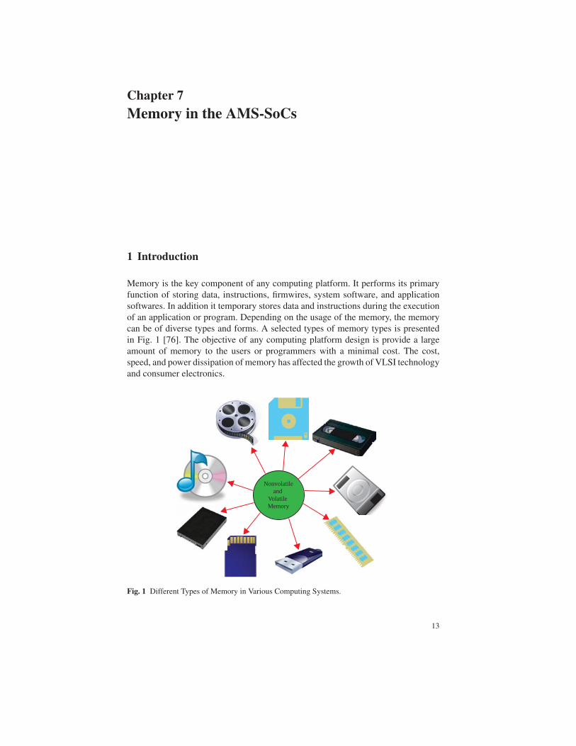
Chapter 7Memory in the AMS-SoCs
1 Introduction
Memory is the key component of any computing platform. It performs its primary
function of storing data, instructions, firmwires, system software, and application
softwares. In addition it temporary stores data and instructions during the execution
of an application or program. Depending on the usage of the memory, the memory
can be of diverse types and forms. A selected types of memory types is presented
in Fig. 1 [76]. The objective of any computing platform design is provide a large
amount of memory to the users or programmers with a minimal cost. The cost,
speed, and power dissipation of memory has affected the growth of VLSI technology
and consumer electronics.
Nonvolatileand
Volatile Memory
Fig. 1 Different Types of Memory in Various Computing Systems.
13
76
References
1. DRAM Technology. http://smithsonianchips.si.edu/ice/cd/MEMORY97/SEC07.PDF. Accessed on 26 Oct 2013
2. Erasable Programmable Read-Only Memory (EPROM). http://www.siliconfareast.com/eprom.htm. Accessed on 10 Nov 2013
3. Flash Technology. http://smithsonianchips.si.edu/ice/cd/MEM96/SEC10.pdf. Accessed on 17 Sep 2013
4. ROM, EPROM, & EEPROM Technology. http://smithsonianchips.si.edu/ice/cd/MEM96/SEC09.pdf. Accessed on 17 Sep 2013
5. SRAM Technology. http://smithsonianchips.si.edu/ice/cd/MEM96/SEC08.pdf. Accessed on 26 Oct 2013
6. Understanding DRAM Specifications. http://www.cs.albany.edu/˜sdc/CSI404/dramperf.pdf (1996). Accessed on 28 Oct 2013
7. Direct Rambus DRAM (DRDRAM). http://www.pcguide.com/ref/ram/techDRDRAM-c.html (2001). Accessed on 13 Oct 2013
8. Synchronous Graphics RAM (SGRAM). http://www.pcguide.com/ref/video/techSGRAM-c.html (2001). Accessed on 02 Nov 2013
9. Video RAM (VRAM). http://www.pcguide.com/ref/video/techVRAM-c.html (2001). Accessed on 02 Nov 2013
10. Window RAM (WRAM). http://www.pcguide.com/ref/video/techWRAM-c.html (2001). Accessed on 02 Nov 2013
11. Akinaga, H., Shima, H.: Resistive Random Access Memory (ReRAM) Based on Metal Ox-ides. Proceedings of the IEEE 98(12), 2237–2251 (2010). DOI 10.1109/JPROC.2010.2070830
12. Amelifard, B., Fallah, F., Pedram, M.: Reducing the Sub-threshold and Gate-tunneling Leak-age of SRAM Cells using Dual-Vt and Dual-Tox Assignment. In: Proceedings of the DesignAutomation and Test in Europe, pp. 1–6 (2006)
13. Arandilla, C.D.C., Alvarez, A.B., Roque, C.R.K.: Static Noise Margin of 6T SRAM Cell in90-nm CMOS. In: Proceedings of the UKSim 13th International Conference on ComputerModelling and Simulation, pp. 534–539 (2011). DOI 10.1109/UKSIM.2011.108
14. Paz de Araujo, C., McMillan, L., Joshi, V., Solayappan, N., Lim, M., Arita, K., Moriwaki,N., Hirano, H., Baba, T., Shimada, Y., Sumi, T., Fujii, E., Otsuki, T.: The Future of Ferro-electric Memories. In: Digest of Technical Papers IEEE International Solid-State CircuitsConference, pp. 268–269 (2000). DOI 10.1109/ISSCC.2000.839779
15. Arimoto, K., Morishita, F., Hayashi, I., Dosaka, K., Shimano, H., Ipposhi, T.: A High-DensityScalable Twin Transistor RAM (TTRAM) With Verify Control for SOI Platform MemoryIPs. IEEE Journal of Solid-State Circuits 42(11), 2611–2619 (2007). DOI 10.1109/JSSC.2007.907185
16. Atwood, G., Chae, S.I., Shim, S.S.Y.: Next-Generation Memory. Computer 46(8), 21–22(2013). DOI 10.1109/MC.2013.285
17. Balwant Raj, A.S., Singh, G.: Analysis of Power Dissipation in DRAM Cells Design forNanoScale Memories. International Journal of Information Technology and KnowledgeManagement 2, 371–374 (2009)
18. Bassin, C., Fazan, P., Xiong, W., Cleavelin, C.R., Schulz, T., Schruefer, K., Gostkowski,M., Patruno, P., Maleville, C., Nagoga, M., Okhonin, S.: Retention Characteristics of Zero-Capacitor Ram (Z-RAM) Cell Based On FinFET and Tri-Gate Devices. In: Proceedingsof the IEEE International SOI Conference, pp. 203–204 (2005). DOI 10.1109/SOI.2005.1563588
19. Blomster, K.A.: Schemes For Reducing Power and Delay In SRAMs. Master’s thesis, Schoolof Electrical Engineering and Computer Science, Washington State University (2006)
20. Butler, W.H., Zhang, X.G., Schulthess, T.C., MacLaren, J.M.: Spin-Dependent Tunnel-ing Conductance of Fe|MgO|Fe Sandwiches. Physical Review B 63, 054,416 (2001).DOI 10.1103/PhysRevB.63.054416. URL http://link.aps.org/doi/10.1103/PhysRevB.63.054416
77
21. Calhoun, B.H., Chandrakasan, A.P.: Static noise margin variation for sub-threshold sram in65-nm cmos. IEEE Journal of Solid-State Circuits 41(7), 1673–1679 (2006). DOI 10.1109/JSSC.2006.873215
22. Carlson, I., Andersson, S., Natarajan, S., Alvandpour, A.: A High Density, Low Leakage,5T SRAM for Embedded Caches. In: Proceeding of the 30th European Solid-State CircuitsConference, pp. 215–218 (2004). DOI 10.1109/ESSCIR.2004.1356656
23. Chang, L., Montoye, R.K., Nakamura, Y., Batson, K.A., Eickemeyer, R.J., Dennard, R.H.,Haensch, W., Jamsek, D.: An 8T-SRAM for Variability Tolerance and Low-Voltage Oper-ation in High-Performance Caches. IEEE Journal of Solid-State Circuits 43(4), 956–963(2008). DOI 10.1109/JSSC.2007.917509
24. Chen, Y.N., Fan, M.L., Hu, V.H., Su, P., Chuang, C.T.: Design and Analysis of Robust Tun-neling FET SRAM. IEEE Transactions on Electron Devices 60(3), 1092–1098 (2013). DOI10.1109/TED.2013.2239297
25. Chevallier, C.J., Siau, C.H., Lim, S.F., Namala, S., Matsuoka, M., Bateman, B., Rinerson, D.:A 0.13 μm 64Mb Multi-Layered Conductive Metal-Oxide Memory. In: Digest of TechnicalPapers IEEE International Solid-State Circuits Conference, pp. 260–261 (2010). DOI 10.1109/ISSCC.2010.5433945
26. Cobley, R.A., Wright, C.D.: Parameterized SPICE Model For a Phase-Change RAM Device.IEEE Transactions on Electron Devices 53(1), 112–118 (2006). DOI 10.1109/TED.2005.860642
27. Crippa, L., Micheloni, R., Motta, I., Sangalli, M.: Nonvolatile Memories: NOR vs. NANDArchitectures. In: R. Micheloni, G. Campardo, P. Olivo (eds.) Memories in WirelessSystems, Signals and Communication Technology, pp. 29–53. Springer Berlin Heidelberg(2008). DOI 10.1007/978-3-540-79078-5 2. URL http://dx.doi.org/10.1007/978-3-540-79078-5_2
28. Crisp, R.: Direct rambus technology: the new main memory standard. IEEE Micro 17(6),18–28 (1997). DOI 10.1109/40.641593
29. Cuppu, V., Jacob, B., Davis, B., Mudge, T.: A Performance Comparison of ContemporaryDRAM Architectures. In: Proceedings of the 26th International Symposium on ComputerArchitecture, pp. 222–233 (1999)
30. DeMone, P.: Direct Rambus Memory. http://www.realworldtech.com/rambus-basics/ (1999). Accessed on 13 Oct 2013
31. Diodato, P.W., Clemens, J.T., Troutman, W.W., Lindenberger, W.S.: A Reusable EmbeddedDRAM Macrocell. In: Proceedings of the IEEE Custom Integrated Circuits Conference, pp.337–340 (1997). DOI 10.1109/CICC.1997.606642
32. Dong, W., Li, P., Huang, G.M.: SRAM dynamic stability: Theory, Variability and Analysis.In: Proceedings of IEEE/ACM International Conference on Computer-Aided Design, pp.378–385 (2008). DOI 10.1109/ICCAD.2008.4681601
33. Dong, X., Jouppi, N., Xie, Y.: PCRAMsim: System-Level Performance, Energy, and AreaModeling for Phase-Change RAM. In: Digest of Technical Papers IEEE/ACM InternationalConference on Computer-Aided Design, pp. 269–275 (2009)
34. Fan, M.L., Wu, Y.S., Hu, V.H., Su, P., Chuang, C.T.: Investigation of Static Noise Margin ofFinFET SRAM Cells in Sub-Threshold Region. In: Proceedings of the IEEE InternationalSOI Conference, pp. 1–2 (2009). DOI 10.1109/SOI.2009.5318785
35. Grossar, E., Stucchi, M., Maex, K., Dehaene, W.: Read Stability and Write-Ability Analysisof SRAM Cells for Nanometer Technologies. IEEE Journal of Solid-State Circuits 41(11),2577–2588 (2006). DOI 10.1109/JSSC.2006.883344
36. Guo, Z., Balasubramanian, S., Zlatanovici, R., King, T.J., Nikolic, B.: FinFET-based SRAMDesign. In: Proceedings of the International Symposium on Low Power Electronics andDesign, pp. 2–7 (2005). DOI 10.1109/LPE.2005.195476
37. Gupta, R., Nemati, F., Robins, S., Yang, K., Gopalakrishnan, V., Sundarraj, J., Chopra, R.,Roy, R., Cho, H.J., Maszara, W.P., Mohapatra, N.R., Wuu, J., Weiss, D., Nakib, S.: 32nmHigh-Density High-Speed T-RAM Embedded Memory Technology. In: Proceedings of theIEEE International Electron Devices Meeting (IEDM), pp. 12.1.1–12.1.4 (2010). DOI 10.1109/IEDM.2010.5703345
78
38. Haque Chowdhur, M.A., Kimy, K.H.: A Survey of Flash Memory Design and Implemen-tation of Database in Flash Memory. In: Proceedings of the 3rd International Conferenceon Intelligent System and Knowledge Engineering, vol. 1, pp. 1256–1259 (2008). DOI10.1109/ISKE.2008.4731123
39. Harari, E.: Flash Memory - The Great Disruptor! In: Solid-State Circuits Conference Digestof Technical Papers (ISSCC), 2012 IEEE International, pp. 10–15 (2012). DOI 10.1109/ISSCC.2012.6176930
40. Hong, S.I., McKee, S.A., Salinas, M.H., Klenke, R.H., Aylor, J.H., Wulf, W.A.: Access Orderand Effective Bandwidth For Streams On A Direct Rambus Memory. In: Proceedings FifthInternational Symposium On High-Performance Computer Architecture, pp. 80–89 (1999).DOI 10.1109/HPCA.1999.744337
41. Hu, Z., Juang, P., Diodato, P., Kaxiras, S., Skadron, K., Martonosi, M., Clark, D.W.: Manag-ing Leakage For Transient Data: Decay and Quasi-Static 4T Memory Cells. In: Proceedingsof the International Symposium on Low Power Electronics and Design, pp. 52–55 (2002).DOI 10.1109/LPE.2002.146708
42. Jung, M., Shalf, J., Kandemir, M.: Design of a Large-scale Storage-class RRAM System.In: Proceedings of the 27th International ACM Conference on International Conference onSupercomputing, ICS ’13, pp. 103–114. ACM, New York, NY, USA (2013). DOI 10.1145/2464996.2465004. URL http://doi.acm.org/10.1145/2464996.2465004
43. Karl, E., Wang, Y., Ng, Y.G., Guo, Z., Hamzaoglu, F., Bhattacharya, U., Zhang, K., Mistry,K., Bohr, M.: A 4.6GHz 162Mb SRAM Design in 22nm Tri-Gate CMOS Technology WithIntegrated Active VMIN-Enhancing Assist Circuitry. In: Proceedings of the IEEE Inter-national Solid-State Circuits Conference Digest of Technical Papers (ISSCC), pp. 230–232(2012). DOI 10.1109/ISSCC.2012.6176988
44. Keeth, B., Baker, R.J., Johnson, B., Lin, F.: DRAM Circuit Design: Fundamental and High-Speed Topics. IEEE Press Series on Microelectronic Systems. Wiley (2008). URL http://books.google.com/books?id=TgW3LTubREQC
45. Kim, K.: Future Memory Technology: Challenges and Opportunities. In: Proceedings of theInternational Symposium on VLSI Technology, Systems and Applications, pp. 5–9 (2008).DOI 10.1109/VTSA.2008.4530774
46. Lai, S., Lowrey, T.: OUM - A 180 nm nonvolatile memory cell element technology for standalone and embedded applications. In: Technical Digest International Electron Devices Meet-ing, pp. 36.5.1–36.5.4 (2001). DOI 10.1109/IEDM.2001.979636
47. Lee, H.Y., Chen, P.S., Wu, T.Y., Chen, Y.S., Wang, C.C., Tzeng, P.J., Lin, C.H., Chen, F.,Lien, C.H., Tsai, M.J.: Low Power and High Speed Bipolar Switching With a Thin ReactiveTi Buffer Layer in Robust HfO2 based RRAM. In: Proceedings of the IEEE InternationalElectron Devices Meeting, pp. 1–4 (2008). DOI 10.1109/IEDM.2008.4796677
48. Li, J., Ndai, P., Goel, A., Salahuddin, S., Roy, K.: Design Paradigm for Robust Spin-TorqueTransfer Magnetic RAM (STT MRAM) From Circuit/Architecture Perspective. IEEE Trans-actions on Very Large Scale Integration (VLSI) Systems 18(12), 1710–1723 (2010). DOI10.1109/TVLSI.2009.2027907
49. Li, Y., Lu, C.S.: Characteristic Comparison of SRAM Cells with 20 nm Planar MOSFET,Omega FinFET and Nanowire FinFET. In: Proceedings of the Sixth IEEE Conference onNanotechnology, pp. 339–342 (2006). DOI 10.1109/NANO.2006.247646
50. Li, Y., Quader, K.N.: NAND Flash Memory: Challenges and Opportunities. Computer 46(8),23–29 (2013). DOI 10.1109/MC.2013.190
51. Liu, Jamie and Jaiyen, Ben and Kim, Yoongu and Wilkerson, Chris and Mutlu, Onur: AnExperimental Study of Data Retention Behavior in Modern DRAM Devices: ImplicationsFor Retention Time Profiling Mechanisms. In: Proceedings of the 40th Annual Interna-tional Symposium on Computer Architecture, pp. 60–71. ACM, New York, NY, USA (2013).DOI 10.1145/2485922.2485928. URL http://doi.acm.org/10.1145/2485922.2485928
52. Lohstroh, J.: Static and Dynamic Noise Margins of Logic Circuits. IEEE Journal of Solid-State Circuits 14(3), 591–598 (1979). DOI 10.1109/JSSC.1979.1051221

79
53. Luk, W.K., Cai, J., Dennard, R.H., Immediato, M.J., Kosonocky, S.V.: A 3-Transistor DRAMCell with Gated Diode for Enhanced Speed and Retention Time. Digest of Technical PapersSymposium on VLSI Circuits pp. 184–185 (2006)
54. Luk, W.K., Dennard, R.H.: A Novel Dynamic Memory Cell With Internal Voltage Gain.IEEE Journal of Solid-State Circuits 40(4), 884–894 (2005)
55. Makosiej, A., Kashyap, R.K., Vladimirescu, A., Amara, A., Anghel, C.: A 32nm Tunnel FETSRAM For Ultra Low Leakage. In: Proceedings of the IEEE International Symposium onCircuits and Systems (ISCAS), pp. 2517–2520 (2012). DOI 10.1109/ISCAS.2012.6271814
56. Meyer, R., Schloss, L., Brewer, J., Lambertson, R., Kinney, W., Sanchez, J., Rinerson, D.:Oxide Dual-Layer Memory Element For Scalable Non-Volatile Cross-Point Memory Tech-nology. In: Proceedings of the 9th Annual Non-Volatile Memory Technology Symposium,pp. 1–5 (2008). DOI 10.1109/NVMT.2008.4731194
57. Mohammad, B., Homouz, D., Elgabra, H.: Robust Hybrid Memristor-CMOS Memory: Mod-eling and Design. IEEE Transactions on Very Large Scale Integration (VLSI) Systems21(11), 2069–2079 (2013). DOI 10.1109/TVLSI.2012.2227519
58. Mohanty, S.P., Kougianos, E.: DOE-ILP Assisted Conjugate-Gradient Optimization of High-κ/Metal-Gate Nano-CMOS SRAM. IET Computers & Digital Techniques 6(4), 240–248(2012)
59. Mohanty, S.P., Singh, J., Kougianos, E., Pradhan, D.K.: Statistical DOE-ILP Based Power-Performance-Process (P3) Optimization of Nano-CMOS SRAM. Elsevier The VLSI Inte-gration Journal 45(1), 33–45 (2012)
60. Moore, S.K.: Masters of Memory. IEEE Spectrum 44(1), 45–49 (2007). DOI 10.1109/MSPEC.2007.273045
61. Morishita, F., Noda, H., Gyohten, T., Okamoto, M., Ipposhi, T., Maegawa, S., Dosaka, K.,Arimoto, K.: A Capacitorless Twin-Transistor Random Access Memory (TTRAM) on SOI.In: Proceedings of the IEEE Custom Integrated Circuits Conference, pp. 435–438 (2005).DOI 10.1109/CICC.2005.1568699
62. Mormann, A.: Burst and Latency Requirements Drive EDO and BEDO DRAM Standards.In: Digest of Papers Technologies for the Information Superhighway, pp. 356–359 (1996).DOI 10.1109/CMPCON.1996.501795
63. Mukherjee, V., Mohanty, S.P., Kougianos, E., Allawadhi, R., Velagapudi, R.: Gate LeakageCurrent Analysis in READ/WRITE/ IDLE States of a SRAM Cell. In: Proceedings of theIEEE Region 5 Conference, pp. 196–200 (2006). DOI 10.1109/TPSD.2006.5507432
64. Nalam, S., Calhoun, B.H.: Asymmetric Sizing in A 45nm 5T SRAM To Improve Read Sta-bility Over 6T. In: Proceeding of the IEEE Custom Integrated Circuits Conference, pp.709–712 (2009). DOI 10.1109/CICC.2009.5280733
65. Nalam, S., Calhoun, B.H.: 5T SRAM With Asymmetric Sizing for Improved Read Stability.IEEE Journal of Solid-State Circuits 46(10), 2431–2442 (2011). DOI 10.1109/JSSC.2011.2160812
66. Nemati, F., Plummer, J.D.: A Novel Thyristor-Based SRAM Cell (T-RAM) For High-Speed,Low-Voltage, Giga-Scale Memories. In: Technical Digest International Electron DevicesMeeting, pp. 283–286 (1999). DOI 10.1109/IEDM.1999.824152
67. Noda, K., Matsui, K., Imai, K., Inoue, K., Tokashiki, K., Kawamoto, H., Yoshida, K., Takeda,K., Nakamura, N., Kimura, T., Toyoshima, H., Koishikawa, Y., Maruyama, S., Saitoh, T.,Tanigawa, T.: A 1.9-μm2 Loadless CMOS Four-Transistor Sram Cell In A 0.18-μm LogicTechnology. In: Technical Digest of International Electron Devices Meeting, pp. 643–646(1998). DOI 10.1109/IEDM.1998.746440
68. Okhonin, S., Nagoga, M., Sallese, J.M., Fazan, P.: A Capacitor-Less 1T-DRAM Cell. IEEEElectron Device Letters 23(2), 85–87 (2002). DOI 10.1109/55.981314
69. Okobiah, O.: Exploring Process-Variation Tolerant Design of Nanoscale Sense AmplifierCircuits. Master’s thesis, Department of Computer Science and Engineering, University ofNorth Texas, Denton, TX (2010)
70. Owen, W.H., Tchon, W.E.: E2PROM Product Issues and Technology Trends. In: Proceedingsof the VLSI and Microelectronic Applications in Intelligent Peripherals and their Intercon-nection Networks, pp. 1/17–1/19 (1989). DOI 10.1109/CMPEUR.1989.93334

80
71. Pagiamtzis, K., Sheikholeslami, A.: Content-Addressable Memory (CAM) Circuits and Ar-chitectures: A Tutorial and Survey. Solid-State Circuits, IEEE Journal of 41(3), 712–727(2006). DOI 10.1109/JSSC.2005.864128
72. Parkin, S.S.P., Kaiser, C., Panchula, A., Rice, P.M., Hughes, B., Samant, M., Yang, S.H.:Giant tunnelling magnetoresistance at room temperature with MgO (100) tunnel barriers.Nature Materials 3, 862–867 (2004). DOI 10.1038/nmat1256
73. Pavan, P., Bez, R., Olivo, P., Zanoni, E.: Flash Memory Cells – An Overview. Proceedingsof the IEEE 85(8), 1248–1271 (1997). DOI 10.1109/5.622505
74. Pavlov, A., Sachdev, M.: CMOS SRAM Circuit Design and Parametric Test in Nano-ScaledTechnologies: Process-Aware SRAM Design and Test. Springer Science and Business MediaB.V. (2008)
75. Philpy, S.T., Kamp, D.A., Derbenwick, G.F.: Nonvolatile and SDRAM Ferroelectric Memo-ries For Aerospace Applications. In: Proceedings of the IEEE Aerospace Conference, vol. 4,pp. 2294–2299 (2004). DOI 10.1109/AERO.2004.1368023
76. Quader, K.N.: Flash Memory at a Cross-Road: Challenges & Opportunities. In: Proceedingsof the 4th IEEE International Memory Workshop, pp. 1–4 (2012). DOI 10.1109/IMW.2012.6213639
77. Raj, B., Saxena, A.K., Dasgupta, S.: Nanoscale FinFET Based SRAM Cell Design: Anal-ysis of Performance Metric, Process Variation, Underlapped FinFET, and Temperature Ef-fect. IEEE Circuits and Systems Magazine 11(3), 38–50 (2011). DOI 10.1109/MCAS.2011.942068
78. Reddy, G.K., Jainwal, K., Singh, J., Mohanty, S.P.: Process Variation Tolerant 9T SRAMBitcell Design. In: Proceedings of the 13th International Symposium on Quality ElectronicDesign, pp. 493–497 (2012)
79. Rodriguez, N., Cristoloveanu, S., Gamiz, F.: Novel Capacitorless 1T-DRAM Cell for 22-nmNode Compatible With Bulk and SOI Substrates. IEEE Transactions on Electron Devices58(8), 2371–2377 (2011). DOI 10.1109/TED.2011.2147788
80. Roy, R., Nemati, F., Young, K., Bateman, B., Chopra, R., Jung, S.O., Show, C., Cho, H.J.:Thyristor-Based Volatile Memory in Nano-Scale CMOS. In: Digest of Technical PapersIEEE International Solid-State Circuits Conference, pp. 2612–2621 (2006). DOI 10.1109/ISSCC.2006.1696327
81. Sakode, V., Lombardi, F., Han, J.: Cell Design and Comparative Evaluation of A Novel 1TMemristor-Based Memory. In: Proceedings of the IEEE/ACM International Symposium onNanoscale Architectures (NANOARCH), pp. 152–159 (2012)
82. Salling, C., Yang, K.J., Gupta, R., Hayes, D., Tamayo, J., Gopalakrishnan, V., Robins, S.:Reliability of Thyristor-Based Memory Cells. In: Proceedings of the IEEE InternationalReliability Physics Symposium, pp. 253–259 (2009). DOI 10.1109/IRPS.2009.5173259
83. Sarwar, S.S., Saqueb, S.A.N., Quaiyum, F., Rashid, A.B.M.H.U.: Memristor-Based Non-volatile Random Access Memory: Hybrid Architecture for Low Power Compact MemoryDesign. IEEE Access 1, 29–34 (2013). DOI 10.1109/ACCESS.2013.2259891
84. Seabaugh, A.: The Tunneling Transistor. IEEE Spectrum 50(10), 35–62 (2013). DOI 10.1109/MSPEC.2013.6607013
85. Seevinck, E., List, F.J., Lohstroh, J.: Static Noise Margin Analysis of MOS SRAM Cells.IEEE Journal of Solid-State Circuits 22(5), 748–754 (1987)
86. Sheikholeslami, A., Gulak, P.G.: A Survey of Circuit Innovations in Ferroelectric Random-Access Memories. Proceedings of the IEEE 88(5), 667–689 (2000). DOI 10.1109/5.849164
87. Sheu, S.S., Cheng, K.H., Chang, M.F., Chiang, P.C., Lin, W.P., Lee, H.Y., Chen, P.S., Chen,Y.S., Wu, T.Y., Chen, F., Su, K.L., Kao, M.J., Tsai, M.J.: Fast-Write Resistive RAM (RRAM)for Embedded Applications. IEEE Design Test of Computers 28(1), 64–71 (2011). DOI10.1109/MDT.2010.96
88. Shin, C., Nikolic, B., Liu, T.J.K., Tsai, C.H., Wu, M.H., Chang, C.F., Liu, T.J.K., Kao, C.Y.,Lin, G.S., Chiu, K.L., Fu, C.S., tzung Tsai, C., Liang, C.W.: Tri-Gate Bulk CMOS Tech-nology For Improved SRAM Scalability. In: Proceedings of the European Solid-State De-vice Research Conference (ESSDERC), pp. 142–145 (2010). DOI 10.1109/ESSDERC.2010.5618437
81
89. Shino, T., Higashi, T., Fujita, K., Ohsawa, T., Minami, Y., Yamada, T., Morikado, M., Naka-jima, H., Inoh, K., Hamamoto, T., Nitayama, A.: Highly Scalable FBC (Floating Body Cell)With 25nm Box Structure For Embedded DRAM Applications. In: Digest of TechnicalPapers Symposium on VLSI Technology, pp. 132–133 (2004). DOI 10.1109/VLSIT.2004.1345435
90. Shiva, S.G.: e-Study Guide for: Computer Organization, Design, and Architecture. Con-tent Technology Inc. (2012). URL http://books.google.com/books?id=Jayapuotyg8C
91. Singh, J., Mathew, J., Mohanty, S.P., Pradhan, D.K.: A Nano-CMOS Process Variation In-duced Read Failure Tolerant SRAM Cell. In: Proceedings of the IEEE International Sympo-sium on Circuits and Systems, pp. 3334–3337 (2008). DOI 10.1109/ISCAS.2008.4542172
92. Singh, J., Mathew, J., Pradhan, D.K., Mohanty, S.P.: A Subthreshold Single Ended I/OSRAM Cell Design for Nanometer CMOS Technologies. In: Proceedings of the IEEE Inter-national SoC Conference, pp. 243–246 (2008)
93. Singh, J., Mohanty, S.P., Pradhan, D.K.: Robust SRAM Designs and Analysis. SpringerScience and Business Media (2012)
94. Song, Y.J., Jeong, G., Baek, I.G., Choi, J.: What Lies Ahead for Resistance-Based MemoryTechnologies? Computer 46(8), 30–36 (2013). DOI 10.1109/MC.2013.221
95. Stein, K.U., Sihling, A., Doering, E.: Storage Array and Sense/refresh Circuit for Single-Transistor Memory Cells. IEEE Journal of Solid-State Circuits 7(5), 336–340 (1972)
96. Tanaka, T., Yoshida, E., Miyashita, T.: Scalability Study On A Capacitorless 1T-DRAM:From Single-Gate PD-SOI To Double-Gate FinDRAM. In: Technical Digest of IEEE Inter-national Electron Devices Meeting, pp. 919–922 (2004). DOI 10.1109/IEDM.2004.1419332
97. Tarigopula, S.: A CAM Based High-Performance Classifier-Scheduler For A Video NetworkProcessor. Master’s thesis, Department of Computer Science and Engineering, University ofNorth Texas, Denton, TX (2007)
98. Thakral, G.: Process-Voltage-Temperature Aware Nanoscale Circuit Optimization. Ph.D.thesis, Computer Science and Engineering, University of North Texas, Denton (December2010)
99. Thakral, G., Mohanty, S.P., Ghai, D., Pradhan, D.K.: A Combined DOE-ILP Based Powerand Read Stability Optimization in Nano-CMOS SRAM. In: Proceedings of the 23rd Inter-national Conference on VLSI Design, pp. 45–50 (2010)
100. Thakral, G., Mohanty, S.P., Ghai, D., Pradhan, D.K.: A DOE-ILP Assisted Conjugate-Gradient Based Power and Stability Optimization in High-κ Nano-CMOS SRAM. In: Pro-ceedings of the 20th ACM Great Lakes Symposium on VLSI, pp. 323–328 (2010)
101. Thakral, G., Mohanty, S.P., Ghai, D., Pradhan, D.K.: P3 (power-performance-process) op-timization of nano-CMOS SRAM using statistical DOE-ILP. In: Proceedings of the 11thInternational Symposium on Quality of Electronic Design, pp. 176–183 (2010)
102. Thakral, G., Mohanty, S.P., Pradhan, D.K., Kougianos, E.: DOE-ILP Based SimultaneousPower and Read Stability Optimization in Nano-CMOS SRAM. Journal Low Power Elec-tronics 6(3), 390–400 (2010)
103. Thean, V.Y.A., Leburton, J.P.: Flash Memory: Towards Single-Electronics. IEEE Potentials21(4), 35–41 (2002). DOI 10.1109/MP.2002.1044216
104. Thornton, C.: Overview Programmable Read-Only-Memories. In: Digest of Technical PapersIEEE International Solid-State Circuits Conference, vol. XX, pp. 180–181 (1977). DOI10.1109/ISSCC.1977.1155709
105. Tseng, Y.H., Zhang, Y., Okamura, L., Yoshihara, T.: A New 7-Transistor SRAM Cell DesignWith High Read Stability. In: Proceedings of the International Conference on ElectronicDevices, Systems and Applications (ICEDSA), pp. 43–47 (2010). DOI 10.1109/ICEDSA.2010.5503104
106. Verma, N., Chandrakasan, A.P.: A 256 kb 65 nm 8T Subthreshold SRAM Employing Sense-Amplifier Redundancy. IEEE Journal of Solid-State Circuits 43(1), 141–149 (2008). DOI10.1109/JSSC.2007.908005
82
107. Wang, D.T.: Modern DRAM Memory Systems: Performance Analysis and Scheduling Al-gorithm. Ph.D. thesis, Department of Electrical and Computer Engineering, University ofMaryland, College Park, MD, USA (2005). Accessed on 14 Sep 2013
108. Wang, J., Nalam, S., Calhoun, B.: Analyzing Static and Dynamic Write Margin For Nanome-ter SRAMs. In: Proceedings of the ACM/IEEE International Symposium on Low PowerElectronics and Design, pp. 129–134 (2008). DOI 10.1145/1393921.1393954
109. Wann, C., Wong, R., Frank, D.J., Mann, R., Ko, S.B., Croce, P., Lea, D., Hoyniak, D., Lee,Y.M., Toomey, J., Weybright, M., Sudijono, J.: SRAM Cell Design For Stability Methodol-ogy. In: VLSI Technology, 2005. (VLSI-TSA-Tech). 2005 IEEE VLSI-TSA InternationalSymposium on, pp. 21–22 (2005). DOI 10.1109/VTSA.2005.1497065
110. Weste, N.H.E., Harris, D.M.: CMOS VLSI Design : A Circuits and Systems Perspective,Fourth Edition edn. Addison-Wesley (2011)
111. Williams, T.: 1 Terabit on a Chip ? New Memory Technology Rises to Challenge NANDFlash. http://www.rtcmagazine.com/articles/view/102293 (2011). Ac-cessed on 24 Sep 2013
112. Xu, W., Zhang, T., Chen, Y.: Design of Spin-Torque Transfer Magnetoresistive RAM andCAM/TCAM with High Sensing and Search Speed. IEEE Transactions on Very Large ScaleIntegration (VLSI) Systems 18(1), 66–74 (2010). DOI 10.1109/TVLSI.2008.2007735
113. Yamaoka, M., Osada, K., Tsuchiya, R., Horiuchi, M., Kimura, S., Kawahara, T.: Low PowerSRAM Menu For SoC Application Using Yin-Yang-Feedback Memory Cell Technology. In:VLSI Circuits, 2004. Digest of Technical Papers. 2004 Symposium on, pp. 288–291 (2004).DOI 10.1109/VLSIC.2004.1346590
114. Zhang, B., Arapostathis, A., Nassif, S., Orshansky, M.: Analytical Modeling of SRAM Dy-namic Stability. In: Proceedings of the IEEE/ACM International Conference on Computer-Aided Design, pp. 315–322 (2006). DOI 10.1109/ICCAD.2006.320052
115. Zhang, W., Li, T.: Characterizing and Mitigating the Impact of Process Variations on PhaseChange Based Memory Systems. In: Proceedings of the 42nd Annual IEEE/ACM Interna-tional Symposium on Microarchitecture, pp. 2–13 (2009)
Chapter 8Mixed-Signal Circuit and System Design Flow
1 Introduction
A typical Analog/Mixed-Signal System-on-a-Chip (AMS-SoC) has a variety of components including digital
processors, analog circuitry, RF circuitry, true mixed-signal circuitry integrated together to achieve cost and
performance trade-offs [118, 67, 90, 62]. In addition there is significant software presence in the AMS-SoC
in the form of firmware, system software (operating system), and application software. The design of power
supply components which are battery packs and possibly accompanied by solar panel involves different design
cycles. This chapter will focus on the hardware components involving analog, radio frequency (RF), digital,
and mixed-signal circuitry.
In the hardware components of the AMS-SoC, the digital circuitry performs most of the back-end process-
ing of the data. The mixed-signal, analog, and RF components are present for front-end processing including
communications and interfacing. In a typical design style the digital components contain much more number
of transistors as compared to the mixed-signal, analog, and RF components. Of course, the digital designs of
well-defined abstraction like from system to physical level to provide design flexibility to design engineers
through divide-and-conquer approach. However, at the last phase of the AMS-SoC design, all types of compo-
nents (digital, mixed-signal, analog, and RF) are physical designs or layouts. At the circuit and the layout levels
the designs go through analog SPICE simulations for verification and characterization. The complexity of the
AMS-SoC hardware component designs have increased multifolds for many reasons including the following
[90]:
(1) Integration of digital, analog, and mixed-signal functions along with the embedded software needs co-
design for overall AMS-SoC optimization.
(2) New signal processing algorithms and their corresponding architectures provide much serious challenges
in terms of total AMS-SoC power dissipation and performance requirements.
(3) The transistor count has increased tremendously to support the various functionalities of the AMS-SoC.
(4) The rapid change of the process technologies demands consideration of different technology parameters
during the design cycle for simulation and design space exploration.
As a result the AMS-SoC design cycle is long and error prone. The overall design needs diverse skills, such as
analog design, digital design, layout engineering, and design verification. The digital verification is becoming
increasing important and complex. The need for analog verification has also emerged [64]. To make the situa-
tion worse the technically expected for such highly complex AMS-SoCs, the time-to-market has been reduced
significantly. In such a situation, Computer Aided Design (CAD) environments including design and verifica-
tion flows are more important than ever in order to produce error-free, affordable, and functional AMS-SoCs
on time.
15
67
References
1. Alliance: A Complete CAD System for VLSI Design. http://www-soc.lip6.fr/en/recherche/cian/alliance/, ftp://ftp.ece.lsu.edu/pub/koppel/alliance/overview.pdf. Accessed on 04 February2014
2. gEDA project. http://www.geda-project.org/. Accessed on 04 February 20143. GTKWave Waveform Viewer. http://gtkwave.sourceforge.net/. Accessed on 10 February 20144. LAyout System for Individuals (LASI). http://lasihomesite.com/index.htm. Accessed on 10 February 20145. Magic VLSI Layout Tool. http://opencircuitdesign.com/magic/. Accessed on 11 February 20146. Mixed - Mode Mixed - Level Circuit simulator. http://ngspice.sourceforge.net/, http://ngspice.
sourceforge.net/docs/ngspice-manual.pdf. Accessed on 10 February 20147. Netgen. http://opencircuitdesign.com/netgen/. Accessed on 11 February 20148. The Community Enterprise Operating System. http://www.centos.org/. Accessed on 15 Feb 20149. TightVNC software. http://www.tightvnc.com/. Accessed on 15 Feb 2014
10. XCircuit. http://opencircuitdesign.com/xcircuit/. Accessed on 11 February 201411. Xming X Server. http://www.straightrunning.com/XmingNotes/. Accessed on 15 Feb 201412. Open Source Initiative. http://opensource.org/ (1998). Accessed on 10 February 201413. GNU General Public License. https://www.gnu.org/copyleft/gpl.html (2007). Accessed on 10 February
201414. AMAZING PICS: How a Chip is Made. APC Magazine (2009). Accessed on 28 January 201415. Cadence Analog/Mixed-signal Design Methodology. http://www.cadence.com/rl/Resources/overview/
ams_methodology_ov.pdf (2009). Accessed on 07 January 201416. New Approach to Accelerating Analog Layout Surpasses Full Custom and Traditional Automation Methodologies. http:
//www.tannereda.com/images/pdfs/Whitepapers/hiper_devgen_whitepaper.pdf (2010). Ac-cessed on 2 February 2014
17. Pre and Post Layout Electrical Rule Checking using PVS Programmable ERC (PERC). http://s218101435.onlinehome.us/cadence/jan12/Pre_and_Post_Layout_Electrical_Rule_Checking_using_PVS_Programmable.pdf (2011). Accessed on 16 January 2014
18. The Fastest Path to Design Signoff. Cadence Design Systems (2011). Accessed on 28 January 201419. Driving A/MS Innovation: An EDA Ecosystem Approach. http://www.soccentral.com/results.asp?
CatID=488&EntryID=38596 (2012). Accessed on 04 February 201420. Cadence Design Systems, Inc. http://www.cadence.com/ (2014). Accessed on 30 January 201421. Custom IC Design. http://www.cadence.com/products/cic/pages/default.aspx (2014). Accessed on
02 February 201422. Design Simulation and Device Models. http://www.linear.com/designtools/software/ (2014). Accessed
on 10 February 201423. Digital CAD. http://www.silvaco.com/products/digital_cad.html (2014). Accessed on 02 February
201424. Jasper Design Automation, Inc. http://jasper-da.com/ (2014). Accessed on 30 January 201425. Mentor Graphics Corporation. http://www.mentor.com/ (2014). Accessed on 30 January 201426. Microwind. http://www.microwind.net/ (2014). Accessed on 30 January 201427. Silvaco, Inc. http://www.silvaco.com/ (2014). Accessed on 30 January 201428. SMIC-Cadence Analog Mixed-Signal Reference Flow 1.1. http://www.smics.com/eng/design/reference_
flows06.php (2014). Accessed on 04 February 201429. Synopsys, Inc. http://www.synopsys.com/ (2014). Accessed on 30 January 201430. Tanner EDA. http://www.tannereda.com/ (2014). Accessed on 30 January 201431. Tanner EDA Mixed-Signal Design Flow. http://www.tannereda.com/ams (2014). Accessed on 04 February 201432. Abidi, A.A.: Behavioral Modeling of Analog and Mixed Signal IC’s: Case Studies of Analog Circuit Simulation Beyond
SPICE. In: Proceedings of the IEEE Conference on Custom Integrated Circuits, pp. 443–450 (2001). DOI 10.1109/CICC.2001.929819
33. Agarwal, A.: Algorithms for Layout-Aware and Performance Model Driven Synthesis of Analog Circuits. Ph.D. thesis, De-partment of Computer Science & Engineering, University of Cincinnati, Ohio (2005). URL http://rave.ohiolink.edu/etdc/view?acc_num=ucin1132259454
34. Alpert, C.J., Karandikar, S.K., Li, Z., Nam, G.J., Quay, S.T., Ren, H., Sze, C.N., Villarrubia, P.G., Yildiz, M.C.: Techniquesfor Fast Physical Synthesis. Proceedings of the IEEE 95(3), 573–599 (2007). DOI 10.1109/JPROC.2006.890096
35. Amaru, L., Gaillardon, P.E., De Micheli, G.: BDS-MAJ: A BDD Based Logic Synthesis Tool Exploiting Majority LogicDecomposition. In: Proceedings of the 50th ACM/EDAC/IEEE Design Automation Conference, pp. 1–6 (2013)
36. Antao, B., Brodersen, A.: ARCHGEN: Automated Synthesis of Analog Systems. IEEE Transactions on Very Large ScaleIntegration (VLSI) Systems 3(2), 231–244 (1995)
37. Antao, B.A.A., Brodersen, A.J.: Behavioral Simulation for Analog System Design Verification. IEEE Transactions on VeryLarge Scale Integration (VLSI) Systems 3(3), 417–429 (1995). DOI 10.1109/92.406999
38. Appelt, B.K., Tseng, A., Lai, Y.S.: Copper Wire Bonding Experiences From a Manufacturing Perspective. In: Proceedingsof the 18th European Microelectronics and Packaging Conference, pp. 1–4 (2011)
39. Appelt, B.K., Tseng, A., Uegaki, S., Essig, K.: Thin Packaging - What Is Next? In: Proceedings of the 2nd IEEE CPMTSymposium Japan, pp. 1–4 (2012). DOI 10.1109/ICSJ.2012.6523400
68
40. Arafa, A., Wagieh, H., Fathy, R., Ferguson, J., Morgan, D., Anis, M.H., Dessouky, M.: Schematic-Driven Physical Verifica-tion: Fully Automated Solution For Analog IC Design. In: Proceedings of the IEEE International SOC Conference (SOCC),pp. 260–264 (2012). DOI 10.1109/SOCC.2012.6398358
41. Armenti, C.: Managing EDA Tools in a Global Design Environment Part 1. http://blog.zuken.com/index.php/2014/02/managing-eda-tools-in-a-global-design-environment-part-1/ (2014). Accessed on 04February 2014
42. Atienza, D., Bobba, S.K., Poli, M., De Micheli, G., Benini, L.: System-Level Design for Nano-Electronics. In: Proceedingsof the 14th IEEE International Conference on Electronics, Circuits and Systems, pp. 747–751 (2007). DOI 10.1109/ICECS.2007.4511099
43. Bailey, B., Martin, G.: ESL Models and their Application: Electronic System Level Design and Verification in Practice.Embedded Systems. Springer (2009). URL http://books.google.com/books?id=5ILek8YFmx4C
44. Bakeer, H.G., Shaheen, O., Eissa, H.M., Dessouky, M.: Analog, Digital and Mixed-Signal Design Flows. In: Proceedings ofthe 2nd International Design and Test Workshop, pp. 247–252 (2007). DOI 10.1109/IDT.2007.4437470
45. Balakrishnan, K.: A VLSI System for Digital Watermarking in Images. Master’s thesis, Department of Computer Scienceand Engineering, University of South Florida, Tampa, FL (2003)
46. Balasinski, A.: Question: DRC or DfM? Answer: FMEA and ROI. In: Proceedings of the 7th International Symposium onQuality Electronic Design, pp. 788–794 (2006). DOI 10.1109/ISQED.2006.110
47. Bali, S.: “In-Design” Physical Verification is “On-Time” Physical Verification. EDN Network (2009). Accessed on 28January 2014
48. Balkir, S., Dundar, G., Ogrenci, A.S.: Analog VLSI Design Automation. CRC Press (2003)49. Bard, K., Dewey, B., Hsu, M.T., Mitchell, T., Moody, K., Rao, V., Rose, R., Soreff, J., Washburn, S.: Transistor-Level
Tools for High-End Processor Custom Circuit Design at IBM. Proceedings of the IEEE 95(3), 530–554 (2007). DOI10.1109/JPROC.2006.889385
50. Barros, M., Barros, M.F.M., Guilherme, J., Horta, N.: Analog Circuits and Systems Optimization Based on EvolutionaryComputation Techniques. Studies in Computational Intelligence. Springer (2010). URL http://books.google.com/books?id=r\_VfPhGq8wsC
51. Barros, M., Guilherme, J., Horta, N.: Analog Circuits Optimization Based On Evolutionary Computation Techniques.Integration, the VLSI Journal 43(1), 136–155 (2010). DOI http://dx.doi.org/10.1016/j.vlsi.2009.09.001. URL http://www.sciencedirect.com/science/article/pii/S0167926009000406
52. Beenker, G., Conway, J., Schrooten, G., Slenter, A.: Analog CAD for Consumer ICs, pp. 347–367. Kluwer AcademicPublishers (1993)
53. Bekiaris, D., Papanikolaou, A., Stamelos, G., Soudris, D., Economakos, G., Pekmestzi, K.: A Standard-Cell Library Suite ForDeep-Deep Sub-Micron CMOS Technologies. In: Proceedings of the 6th International Conference on Design Technology ofIntegrated Systems in Nanoscale Era, pp. 1–6 (2011). DOI 10.1109/DTIS.2011.5941445
54. Bennour, S., Sallem, A., Kotti, M., Gaddour, E., Fakhfakh, M., Loulou, M.: Application of the PSO technique to the Opti-mization of CMOS Operational Transconductance Amplifiers. In: Proceedings of the 5th International Conference on Designand Technology of Integrated Systems in Nanoscale Era (DTIS), pp. 1–5 (2010). DOI 10.1109/DTIS.2010.5487582
55. Berkcan, E.: MxSICO: A Mixed Analog Digital Compiler: Application to Oversampled A/D Converters. In: Proceedings ofthe IEEE Custom Integrated Circuits Conference, p. 14.9.1 (1990)
56. Berkcan, E.: MxSICO: A Silicon Compiler for Mixed Analog Digital Circuits. In: Proceedings of the IEEE InternationalConference on Computer Design, pp. 33–36 (1990)
57. Berkcan, E., Currin, B.: Module Compilation for Analog and Mixed Analog Digital Circuits. In: Proceedings of the IEEEInternational Symposium on Circuits and Systems, pp. 831–834 (1990)
58. Berkcan, E., Yassa, F.: Towards Mixed Analog / Digital Design Automation: A Review. In: Proceedings of the IEEEInternational Symposium on Circuits and Systems, pp. 809–815 (1990)
59. Bhatti, M.K., Minhas, A.A., Najam-ul Islam, M., Bhatti, M.A., Ul Haque, Z., Khan, S.A.: Curriculum Design Using MentorGraphics Higher Education Program (HEP) For ASIC Designing From Synthesizable HDL To GDSII. In: Proceedings ofIEEE International Conference on Teaching, Assessment and Learning for Engineering, pp. W1D–1–W1D–6 (2012). DOI10.1109/TALE.2012.6360406
60. Bocchi, M., Brunelli, C., De Bartolomeis, C., Magagni, L., Campi, F.: A System Level IP Integration Methodology ForFast SoC Design. In: Proceedings of the International Symposium on System-on-Chip, pp. 127–130 (2003). DOI 10.1109/ISSOC.2003.1267734
61. Brunvand, E.: Digital VLSI Chip Design With Cadence and Synopsys CAD Tools. ADDISON WESLEY Publishing Com-pany Incorporated (2010). URL http://books.google.com/books?id=YippPgAACAAJ
62. Carley, L.R., Gielen, G.G.E., Rutenbar, R.A., Sansen, W.M.C.: Synthesis tools for mixed-signal ics: Progress on frontendand backend strategies. In: Proceedings of the Design Automation Conference, pp. 298–303 (1996). DOI 10.1109/DAC.1996.545590
63. Castro-Lopez, R., Guerra, O., Roca, E., Fernandez, F.V.: An Integrated Layout-Synthesis Approach for Analog ICs. IEEETransactions on Computer-Aided Design of Integrated Circuits and Systems 27(7), 1179–1189 (2008). DOI 10.1109/TCAD.2008.923417
64. Chang, H., Kundert, K.: Verification of Complex Analog and RF IC Designs. Proceedings of the IEEE 95(3), 622–639(2007). DOI 10.1109/JPROC.2006.889384
65. Chen, F.: RF/RF-SoC Overview and Challenges. http://www.vlsi.uwindsor.ca/presentations/chen1w_seminar_1.pdf (2004). Accessed on 24 Nov 2013
66. Chen, Y., Kahng, A.B., Robins, G., Zelikovsky, A., Zheng, Y.: Evaluation of The New OASIS Format For Layout FillCompression. In: Proceedings of the 11th IEEE International Conference on Electronics, Circuits and Systems, pp. 377–382(2004). DOI 10.1109/ICECS.2004.1399697
69
67. Chou, E.Y., Sheu, B.: System-on-a-Chip Design for Modern Communications. IEEE Circuits and Devices Magazine 17(6),12–17 (2001)
68. Coudert, O.: Logic Synthesis and Verification. chap. Logical and Physical Design: A Flow Perspective, pp. 167–196. KluwerAcademic Publishers, Norwell, MA, USA (2002). Accessed on 17 January 2014
69. Coudert, O.: Timing and Design Closure in Physical Design Flows. In: Proceedings of the International Symposium onQuality Electronic Design, pp. 511–516 (2002). DOI 10.1109/ISQED.2002.996796
70. De Jonghe, D., Maricau, E., Gielen, G., McConaghy, T., Tasic, B., Stratigopoulos, H.: Advances in Variation-Aware Mod-eling, Verification, and Testing of Analog ICs. In: Proceedings of the Design, Automation Test in Europe ConferenceExhibition, pp. 1615–1620 (2012). DOI 10.1109/DATE.2012.6176730
71. De Smedt, B., Gielen, G.: Models For Systematic Design and Verification of Frequency Synthesizers. IEEE Transactions onCircuits and Systems II: Analog and Digital Signal Processing 46(10), 1301–1308 (1999). DOI 10.1109/82.799680
72. Degrauwe, M.G.R., Nys, O., Dijkstra, E., Rijmenants, J., Bitz, S., Goffart, B.L.A.G., Vittoz, E.A., Cserveny, S., Meixen-berger, C., van der Stappen, G., Oguey, H.J.: IDAC: An Interactive Design Tool for Analog CMOS Circuits. IEEE Journalof Solid-State Circuits 22(6), 1106–1116 (1987)
73. Dhanwada, N.R., Vemuri, R.: Constraint Allocation in Analog System Synthesis. In: Proceedings of the International Con-ference on VLSI Design, pp. 253–258 (1998)
74. Doboli, A., Vemuri, R.: A VHDL-AMS Compiler and Architecture Generator for Behavioral Synthesis of Analog Systems.In: Proceedings of the Design Automationa and Test in Europe (DATE) Conference, pp. 338–345 (1999)
75. Doboli, A., Vemuri, R.: Behavioral Modeling for High-Level Synthesis of Analog and Mixed-Signal Systems from VHDL-AMS. IEEE Transactions on CAD of Integrated Circuits 22(11), 1504–1520 (2003). DOI 10.1109/TCAD.2003.818302
76. Doboli, A., Vemuri, R.: Exploration-Based High-Level Synthesis of Linear Analog Systems Operating at Low/MediumFrequencies. IEEE Transactions on Computer-Aided Design of Integrated Circuits and Systems 22(11), 1556–1568 (2003).DOI 10.1109/TCAD.2003.818374
77. Economakos, G., Xydis, S.: Optimized Reconfigurable RTL Components for Performance Improvements During High-LevelSynthesis. In: Proceedings of the 12th Euromicro Conference on Digital System Design, Architectures, Methods and Tools,pp. 164–171 (2009). DOI 10.1109/DSD.2009.193
78. Eeckelaert, T., Schoofs, R., Gielen, G., Steyaert, M., Sansen, W.: An Efficient Methodology for Hierarchical Synthesis ofMixed-signal Systems with Fully Integrated Building Block Topology Selection. In: Proceedings of the Conference onDesign, Automation and Test in Europe, pp. 81–86. EDA Consortium, San Jose, CA, USA (2007). URL http://dl.acm.org/citation.cfm?id=1266366.1266386
79. Eleyan, N., Lin, K., Kamal, M., Mohammad, B., Bassett, P.: Semi-Custom Design Flow: Leveraging Place and Route Tools inCustom Circuit Design. http://www2.dac.com/46th/proceedings/slides/02U_2.pdf (2009). Accessedon 07 January 2014
80. Filiol, H., O’Connor, I., Morche, D.: A New Approach For Variability Analysis of Analog ICs. In: Proceedings of the JointIEEE North-East Workshop on Circuits and Systems and TAISA Conference, pp. 1–4 (2009). DOI 10.1109/NEWCAS.2009.5290422
81. Francken, K., Vancorenland, P., Gielen, G.: DAISY: A Simulation-Based High-Level Synthesis Tool for ΔΣ Modulators. In:Proceedings of International Conference on Computer Aided Design, pp. 188–192 (2000)
82. Garitselov, O.: Metamodeling-Based Fast Optimization Of Nanoscale AMS-SoCs. Ph.D. thesis, Computer Science andEngineering, University Of North Texas, Denton, 76203, TX, USA., Denton, TX 76207 (2012)
83. Garitselov, O., Mohanty, S.P., Kougianos, E.: Fast Optimization of Nano-CMOS Mixed-signal Circuits Through AccurateMetamodeling. In: Proceedings of the 12th International Symposium on Quality Electronic Design (ISQED), pp. 1–6 (2011)
84. Garitselov, O., Mohanty, S.P., Kougianos, E.: A Comparative Study of Metamodels for Fast and Accurate Simulation ofNano-CMOS Circuits. IEEE Transactions on Semiconductor Manufacturing 25(1), 26–36 (2012). DOI 10.1109/TSM.2011.2173957
85. Garitselov, O., Mohanty, S.P., Kougianos, E.: Accurate Polynomial Metamodeling-Based Ultra-Fast Bee Colony Optimiza-tion of A Nano-CMOS Phase-Locked Loop. Journal of Low Power Electronics 8(3), 317–328 (2012)
86. Ghai, D.: Variability Aware Low-Power Techniques for Nanoscale Mixed-Signal Circuits. Ph.D. thesis, Computer Scienceand Engineering, University of North Texas, Denton, TX 76203, USA. (2009)
87. Ghai, D., Mohanty, S., Kougianos, E.: Design of Parasitic and Process-Variation Aware Nano-CMOS RF Circuits: A VCOCase Study. IEEE Transactions on Very Large Scale Integration (VLSI) Systems 17(9), 1339–1342 (2009). DOI 10.1109/TVLSI.2008.2002046
88. Ghai, D., Mohanty, S.P., Kougianos, E., Patra, P.: A PVT Aware Accurate Statistical Logic Library For High-κ Metal-gatenano-CMOS. In: Proceedings of the 10th International Symposium on Quality of Electronic Design, pp. 47–54 (2009)
89. Gielen, G., Wambacq, P., Sansen, W.M.: Symbolic Analysis Methods and Applications For Analog Circuits: A TutorialOverview. Proceedings of the IEEE 82(2), 287–304 (1994). DOI 10.1109/5.265355
90. Gielen, G.G.E., Rutenbar, R.A.: Computer-Aided Design of Analog and Mixed-Signal Integrated Circuits. Proceedings ofthe IEEE 88(12), 1825–1854 (2000). DOI 10.1109/5.899053
91. Goering, R.: Cadence Design Tools Tutorial. http://www.vlsi.wpi.edu/cds/. Accessed on 07 December 201392. Goering, R.: How Parasitic-Aware Design Flow Improves Custom/Analog Productiv-
ity. http://www.cadence.com/community/blogs/ii/archive/2011/03/14/how-parasitic-aware-design-improves-custom-analog-productivity.aspx. Accessed on 27July 2012
93. Gopinath, M.: The Characterization and Model Optimization of An Analog Integrated Circuit Standard Cell Library. Master’sthesis, Department of Electrical and Computer Engineering, University of Louisville, Louisville, Kentucky (2004)
70
94. Grabinski, W., Schreurs, D.: Transistor Level Modeling for Analog/RF IC Design. Springer (2006). URL http://books.google.com/books?id=8WsV2YcyzUEC
95. Gray, J.L.: Managing EDA Tool Installations. http://www.coolverification.com/2005/08/managing_eda_to.html (2005). Accessed on 04 February 2014
96. Grimblatt, V.: Tutorial:Digital IC Design. http://www.sase.com.ar/2012/files/2012/09/IC-Design-Flow-SASE-2012.pdf (2012). Accessed on 31 January 2014
97. Gupta, S.K., Hasan, M.M.: KANSYS: a CAD Tool for Analog Circuit Synthesis. In: Proceedings of the InternationalConference on VLSI Design, pp. 333–334 (1996)
98. Ha, D.S.: Cell Libraries to Support VLSI Research and Education. http://www.vtvt.ece.vt.edu/vlsidesign/cell.php (2009). Accessed on 14 February 2014
99. Harjani, R., Rutenbar, R., Carley, L.: OASYS: A Framework for Analog Circuit Synthesis. IEEE Transactions on Computer-Aided Design of Integrated Circuits and Systems 8(12), 1247–1266 (1993)
100. Hegazy, H.: Programmable Electrical Rule Checking. http://www.eetimes.com/document.asp?doc_id=1276155 (2008). Accessed on 07 January 2014
101. Heimlich, M.: Circuit Extraction Techniques Provide Faster Interconnect Modeling and Analysis. High Frequency Electron-ics 6(6), 42–50 (2007)
102. Ho, K.H., Jiang, J.R., Chang, Y.W.: TRECO: Dynamic Technology Remapping for Timing Engineering Change Orders.IEEE Transactions on Computer-Aided Design of Integrated Circuits and Systems 31(11), 1723–1733 (2012). DOI 10.1109/TCAD.2012.2201480
103. Hodson, R.F., Doughty, D.C.: Using Commercial EDA Software in Computer Engineering. In: Proceedings of the ASEEAnnual Conference. American Society for Engineering Education (1997). Accessed on 28 January 2014
104. Horta, N.: Analogue and Mixed-Signal Systems Topologies Exploration Using Symbolic Methods. Analog Integrated Cir-cuits and Signal Processing 31(2), 161–176 (2002). DOI 10.1023/A:1015098112015. URL http://dx.doi.org/10.1023/A%3A1015098112015
105. Horta, N., Franca, J., Leme, C.: Automated High Level Synthesis of Data Conversion Systems. Peregrinus, London (1991)106. Janez Puhan Iztok Fajfar, T.T.A.B.: Transistor Level Optimisation of Digital Cells. Electrotechnical Review 78(1-2), 31–35
(2011)107. Jiang, J.H.R., Devadas, S.: Logic Synthesis in a Nutshell (2008). Accessed on 23 January 2014108. Jin, L., Liu, C., Anan, M.: Open-Source VLSI CAD Tools: A Comparative Study. In: Proceedings of American So-
ciety for Engineering Education, Illinois - Indiana Section Conference (2010). URL http://ilin.asee.org/Conference2010/Papers/A1_Liu_Anan.pdf
109. Johansson, A.: Investigation of Typical 0.13 μm CMOS Technology Timing Effects in a Complex Digital System on Chip.Master’s thesis, Division of Electronics Systems, Department of Electrical Engineering, Linkoping University (2004)
110. Johnson, K.: Characterize Nanometer Analog/RF Circuits. Chip Design Magazine pp. 21–22 (2010). Accessed on 17 January2014
111. Jusuf, G., Gray, P.R., Sangiovanni-Vincentelli, A.L.: CADICS - Cyclic Analog-to-Digital Converter Synthesis. In: Proceed-ings of the International Conference on Computer Aided Design, pp. 286–289 (1990)
112. Jusuf, G., Gray, P.R., Sangiovanni-Vincentelli, A.L.: A Performance-Driven Analog-to-Digital Converter Module Generator.In: Proceedings of the IEEE International Symposium on Circuits and Systems, pp. 2160–2163 (1992)
113. Kahng, A.B.: The Future of Signoff. IEEE Design Test of Computers 28(3), 86–89 (2011). DOI 10.1109/MDT.2011.66114. Kahng, A.B., Lienig, J., Markov, I.L., Hu, J.: VLSI Physical Design: From Graph Partitioning to Timing Closure. Springer
(2011). URL http://books.google.com/books?id=DWUGHyFVpboC115. Kang, S.M., Leblebici, Y.: CMOS Digital Integrated Circuits. Tata McGraw-Hill Education (2003)116. Kao, W.H., Lo, C.Y., Basel, M., Singh, R.: Parasitic Extraction: Current State of The Art and Future Trends. Proceedings of
the IEEE 89(5), 729–739 (2001). DOI 10.1109/5.929651117. Koh, H.Y., Sequin, C.H., Gray, P.R.: OPASYN: A Compiler for CMOS Operational Amplifiers. IEEE Transactions on
Computer-Aided Design of Integrated Circuits and Systems 9(2), 113–125 (1990)118. Kougianos, E., Mohanty, S., Patra, P.: Digital Nano-CMOS VLSI Design Courses in Electrical and Computer Engineering
through Open-Source/Free Tools. In: Proceedings of the International Symposium on Electronic System Design, pp. 265–270(2010). DOI 10.1109/ISED.2010.57
119. Kubar, M.: Novel Optimization Tool for Analog Integrated Circuits Design. Ph.D. thesis, Electrical Engineering and Infor-mation Technology, Czech Technical University, Prague, Czech Republic (2013). 24 Feb 2014
120. Kubar, M., Jakovenko, J.: A Powerful Optimization Tool for Analog Integrated Circuits Design. Radioengineering 22(3),921–931 (2013)
121. Lampaert, K., Gielen, G., Sansen, W.M.C.: Analog Layout Generation Performance and Manufacturability. Kluwer interna-tional series in engineering and computer science: Analog circuits and signal processing. Springer (1999)
122. LaPedus, M.: Whats After CMOS? Semiconductor Engineering (2014). Accessed on 24 January 2014123. Lavagno, L., Martin, G., Scheffer, L.: Electronic Design Automation for Integrated Circuits Handbook - 2 Volume Set. CRC
Press, Inc., Boca Raton, FL, USA (2006)124. Lemaitre, L., McAndrew, C.C., Hamm, S.: ADMS Automatic Device Model Synthesizer. In: Proceedings of the IEEE
Custom Integrated Circuits Conference, pp. 27–30 (2002)125. Lewyn, L.L.: Physical Design and Reliability Issues in Nanoscale Analog CMOS Technologies. In: Proceedings of the
NORCHIP, pp. 1–10 (2009). DOI 10.1109/NORCHP.2009.5397862126. Li, X., Gopalakrishnan, P., Xu, Y., Pileggi, L.T.: Robust Analog/RF Circuit Design With Projection-Based Posynomial
Modeling. In: Proceedings of the International Conference on Computer Aided Design, pp. 855–862 (2004). DOI10.1109/ICCAD.2004.1382694

71
127. Li, X., Le, J., Gopalakrishnan, P., Pileggi, L.T.: Asymptotic Probability Extraction for Nonnormal Performance Distributions.IEEE Transactions on Computer-Aided Design of Integrated Circuits and Systems 26(1), 16–37 (2007). DOI 10.1109/TCAD.2006.882593
128. Lin, M.B.: Synthesis. In: Digital System Designs and Practices Using Verilog HDL and FPGAs. John Wiley (2008). Accessedon 23 January 2014
129. Luo, T.C., Leong, E., Chao, M.C.T., Fisher, P.A., Chang, W.: Mask Versus Schematic - An Enhanced Design-VerificationFlow For First Silicon Success. In: Proceedings of the IEEE International Test Conference, pp. 1–9 (2010). DOI 10.1109/TEST.2010.5699238
130. Mair, H., Xiu, L.: An ASIC Design Flow of Deep Submicron Succeeds on First Pass. In: Proceedings of 5th InternationalConference on Solid-State and Integrated Circuit Technology, pp. 352–355 (1998). DOI 10.1109/ICSICT.1998.785894
131. Manganaro, G., Kwak, S.U., Cho, S., Pulincherry, A.: A Behavioral Modeling Approach To The Design of A Low JitterClock Source. IEEE Transactions on Circuits and Systems II: Analog and Digital Signal Processing 50(11), 804–814 (2003).DOI 10.1109/TCSII.2003.819134
132. del Mar Hershenson, M., Boyd, S.P., Lee, T.H.: GPCAD: A Tool for CMOS OP-AMP Synthesis. In: Proceedings of theInternational Conference on Computer Aided Design, pp. 296–303 (1998)
133. Marques, N.A., Kamon, M., Silveira, L.M., White, J.K.: Generating Compact, Guaranteed Passive Reduced-Order Modelsof 3-D RLC Interconnects. IEEE Transactions on Advanced Packaging 27(4), 569–580 (2004). DOI 10.1109/TADVP.2004.831867
134. Martens, E., Gielen, G.: Top-Down Heterogeneous Synthesis of Analog and Mixed-Signal Systems. In: Proceedings of theDesign, Automation and Test in Europe, pp. 1–6 (2006). DOI 10.1109/DATE.2006.244137
135. McConaghy, T., Eeckelaert, T., Gielen, G.: CAFFEINE: Template-Free Symbolic Model Generation of Analog CircuitsVia Canonical Form Functions and Genetic Programming, year=2005, pages=1082–1087, doi=10.1109/DATE.2005.89,issn=1530-1591,. In: Proceedings of the International Conference on Design, Automation and Test in Europe
136. McCrorie, P., Nizic, M.: Solutions for Mixed-Signal IP, IC, and SoC Implementation. http://www.cadence.com/rl/Resources/white_papers/ms_implementation_wp.pdf (2014). Accessed on 04 February 2014
137. Meeus, W., VanBeeck, K., Goedem, T., Meel, J., Stroobandt, D.: An Overview of Todays High-level Synthesis Tools. DesignAutomation for Embedded Systems 16(3), 31–51 (2012). DOI 10.1007/s10617-012-9096-8. URL http://dx.doi.org/10.1007/s10617-012-9096-8
138. Mehrotra, A., van Ginneken, L., Trivedi, Y.: Design Flow and Methodology for 50M Gate ASIC. In: Proceedings of the Asiaand South Pacific Design Automation Conference, pp. 640–647 (2003). DOI 10.1109/ASPDAC.2003.1195102
139. Meng, K.H., Pan, P.C., Chen, H.M.: Integrated Hierarchical Synthesis Of Analog/RF Circuits With Accurate PerformanceMapping. In: Proceedings of the 12th International Symposium on Quality Electronic Design (ISQED), pp. 1–8 (2011).DOI 10.1109/ISQED.2011.5770817
140. Modi, N.A., Marek-Sadowska, M.: ECO-Map: Technology Remapping for Post-Mask ECO using Simulated Annealing. In:Proceedings of the IEEE International Conference on Computer Design, pp. 652–657 (2008). DOI 10.1109/ICCD.2008.4751930
141. Mohanty, S.P.: Energy and Transient Power Minimization during Behavioral Synthesis. Ph.D. thesis, Department of Com-puter Science and Engineering, University of South Florida, Tampa, USA (2003)
142. Mohanty, S.P.: Ultra-Fast Design Exploration of Nanoscale Circuits through Metamodeling). http://www.cse.unt.edu/˜smohanty/Presentations/2012/Mohanty_SRC-TxACE_Talk_2012-04-27.pdf (2012). Accessedon 13 February 2014
143. Mohanty, S.P., Gomathisankaran, M., Kougianos, E.: Variability-Aware Architecture Level Optimization Techniques forRobust Nanoscale Chip Design. Computers & Electrical Engineering 40(1), 168–193 (2014). DOI http://dx.doi.org/10.1016/j.compeleceng.2013.11.026. URL http://www.sciencedirect.com/science/article/pii/S004579061300308X. 40th-year commemorative issue
144. Mohanty, S.P., Kougianos, E.: Real-Time Perceptual Watermarking Architectures for Video Broadcasting. Journal of Systemsand Software 84(5), 724–738 (2011)
145. Mohanty, S.P., Kougianos, E.: Incorporating Manufacturing Process Variation Awareness in Fast Design Optimization ofNanoscale CMOS VCOs. IEEE Transactions on Semiconductor Manufacturing 27(1), 22–31 (2014). DOI 10.1109/TSM.2013.2291112
146. Mohanty, S.P., Kougianos, E., Pradhan, D.K.: Simultaneous Scheduling and Binding for Low Gate Leakage Nano-Complementary Metal-Oxide-Semiconductor Datapath Circuit Behavioural Synthesis. IET Computers & Digital Techniques2(2), 118–131 (2008)
147. Mohanty, S.P., Kougnianos, E.: Fast Design Exploration of Nanoscale Circuits: Designer’s Guide. http://www.cse.unt.edu/˜smohanty/Projects/CNS_0854182/CNS_0854182_Designer_Guide.pdf (2012). Accessedon 04 February 2014
148. Mohanty, S.P., Ranganathan, N., Balakrishnan, K.: A Dual Voltage-Frequency VLSI Chip for Image Watermarking in DCTDomain. Circuits and Systems II: Express Briefs, IEEE Transactions on 53(5), 394–398 (2006). DOI 10.1109/TCSII.2006.870216
149. Mohanty, S.P., Ranganathan, N., Kougianos, E., Patra, P.: Low-Power High-Level Synthesis for Nanoscale CMOS Circuits.Springer (2008). 0387764739 and 978-0387764733
150. Mohanty, S.P., Ranganathan, N., Krishna, V.: Datapath Scheduling using Dynamic Frequency Clocking. In: Proceedings ofthe IEEE Computer Society Annual Symposium on VLSI, pp. 58–63. IEEE (2002)
151. Mohanty, S.P., Ranganathan, N., Namballa, R.: A VLSI Architecture for Visible Watermarking in a Secure Still DigitalCamera (S2DC) Design. IEEE Transactions on Very Large Scale Integration Systems (TVLSI) 13(8), 1002–1012 (2005)

72
152. Mukherjee, V.: A Dual Dielectric Approach for Performance Aware Reduction of Gate Leakage in Combinational Circuits.Master’s thesis, Department of Computer Science and Engineering, University of North Texas, Denton, TX, USA (2006)
153. Mukherjee, V., Mohanty, S.P., Kougianos, E.: A Dual Dielectric Approach for Performance Aware Gate Tunneling Reductionin Combinational Circuits. In: Proceedings of the 23rd IEEE International Conference on Computer Design, pp. 431–437(2005)
154. Mukhopadhyay, S.: A Generic Method For Variability Analysis of Nanoscale Circuits. In: Proceedings of the InternationalConference on Integrated Circuit Design and Technology, pp. 285–288 (2009). DOI 10.1109/ICICDT.2008.4567297
155. Nishi, Y., Doering, R.: Handbook of Semiconductor Manufacturing Technology. Taylor & Francis (2012). URL http://books.google.com/books?id=PsVVKz\_hjBgC
156. Okobiah, O., Mohanty, S., Kougianos, E.: Geostatistics Inspired Fast Layout Optimization Of Nanoscale CMOS PhaseLocked Loop. In: Proceedings of the 14th International Symposium on Quality Electronic Design, pp. 546–551 (2013).DOI 10.1109/ISQED.2013.6523664
157. Okobiah, O., Mohanty, S.P., Kougianos, E.: Geostatistical-Inspired Fast Layout Optimization of a Nano-CMOS ThermalSensor. IET Circuits, Devices Systems 7(5), 253–262 (2013). DOI 10.1049/iet-cds.2012.0358
158. Pandey, S., Glesner, M., Muhlhauser, M.: Architecture Level Design Space Exploration and Mapping of Hardware. In:Proceedings of the International Symposium on Signals, Circuits and Systems, pp. 553–556 (2005). DOI 10.1109/ISSCS.2005.1511300
159. Peixoto, H.P., Jacome, M.F.: Algorithm and architecture-level design space exploration using hierarchical data flows. In:Proceedings of the IEEE International Conference on Application-Specific Systems, Architectures and Processors, pp. 272–282 (1997). DOI 10.1109/ASAP.1997.606833
160. Petley, G.: VLSI and ASIC Technology Standard Cell Library Design. http://www.vlsitechnology.org/. Ac-cessed on 10 Feb 2014
161. Phelps, R., Krasnicki, M., Rutenbar, R.A., Carley, L.R., Hellums, J.R.: Anaconda: Simulation-Based Synthesis of AnalogCircuits Via Stochastic Pattern Search. IEEE Transactions on Computer-Aided Design of Integrated Circuits and Systems19(6), 703–717 (2000). DOI 10.1109/43.848091
162. Van der Plas, G., Debyser, G., Leyn, F., Lampaert, K., Vandenbussche, J., Gielen, G.G.E., Sansen, W., Veselinovic, P.,Leenarts, D.: AMGIE-A synthesis environment for CMOS analog integrated circuits. IEEE Transactions on Computer-Aided Design of Integrated Circuits and Systems 20(9), 1037–1058 (2001). DOI 10.1109/43.945301
163. Pratt, G., Jarrett, J.: Top-Down Design Methods Bring Back The Useful Schematic Diagram. http://electronicdesign.com/boards/top-down-design-methods-bring-back-useful-schematic-diagram(2001). Accessed on 08 December 2013
164. Priyadarshi, S., Hu, J., Choi, W.H., Melamed, S., Chen, X., Davis, W.R., Franzon, P.D.: Pathfinder 3D: A Flow For System-Level Design Space Exploration. In: Proceedings IEEE International 3D Systems Integration Conference (3DIC), pp. 1–8(2012). DOI 10.1109/3DIC.2012.6262961
165. Rangarajan, S., Chakrabarti, P., Sahais, S., Datta, A., Subramanya, A.: Tutorial T3B: Engineering Change Order (ECO)Phase Challenges and Methodologies for High Performance Design. In: Proceedings of the 27th International Conferenceon VLSI Design, pp. 7–8 (2014). DOI 10.1109/VLSID.2014.118
166. Rashinkar, P., Paterson, P., Singh, L.: System-on-a-Chip Verification: Methodology and Techniques. Springer (2001). URLhttp://books.google.com/books?id=MpzE-kclSMUC
167. Razavi, B.: CMOS Technology Characterization For Analog and RF Design. IEEE Journal of Solid-State Circuits 34(3),268–276 (1999). DOI 10.1109/4.748177
168. Rishabh Agarwal Shailesh Kumar, S.S., Gotra, V.: An Insight into Layout Versus Schematic. http://www.edn.com/design/integrated-circuit-design/4418390/An-insight-into-layout-versus-schematic(2013). Accessed on 07 January 2014
169. Rocha, F.A.E., Martins, R.M.F., Lourenco, N.C.C., Horta, N.C.G.: State-of-the-Art on Automatic Analog IC Sizing. In:Electronic Design Automation of Analog ICs combining Gradient Models with Multi-Objective Evolutionary Algorithms,SpringerBriefs in Applied Sciences and Technology, pp. 7–22. Springer International Publishing (2014). DOI 10.1007/978-3-319-02189-8 2
170. Roy, R., Bhattacharya, D., Boppana, V.: Transistor-Level Optimization of Digital Designs with Flex Cells. Computer 38(2),53–61 (2005). DOI http://doi.ieeecomputersociety.org/10.1109/MC.2005.74
171. Rubin, S.M.: Electric VLSI System. http://www.staticfreesoft.com/index.html. Accessed on 04 February2014
172. Rubin, S.M.: Computer Aids for VLSI Design. R. L. Ranch Press (2009). URL http://books.google.com/books?id=kP0uPwAACAAJ
173. Ruparel, K.N., Chin, C., Fitzgerald, J.: A Vertically Integrated Test Methodology Based On JTAG IEEE 1149.1 StandardInterface. In: Proceedings of the Fourth Annual IEEE International ASIC Conference and Exhibit, pp. P11–4.1–4.4 (1991).DOI 10.1109/ASIC.1991.242912
174. Rutenbar, R.A.: Design Automation for Analog: The Next Generation of Tool Challenges. In: Proceedings of the IEEE/ACMInternational Conference on Computer-Aided Design, pp. 458–460 (2006). DOI 10.1109/ICCAD.2006.320157
175. Rutenbar, R.A., Gielen, G.G.E., Antao, B.A.: Computer-Aided Design of Analog Integrated Circuits and Systems. Wiley-IEEE Press (2002)
176. Sabiro, S.G., Sen, P., Tawfik, M.S.: HiFADiCC: A Prototype Framework of a Highly Flexible Analog to Digital ConvertersSilicon Compiler. In: Proceedings of the IEEE International Symposium on Circuits and Systems, pp. 1114–1117 (1990)
177. Sangiovanni-Vincentelli, A.: The Tides of EDA. IEEE Design Test of Computers 20(6), 59–75 (2003). DOI 10.1109/MDT.2003.1246165
73
178. Sangiovanni-Vincentelli, A.: Corsi e ricorsi: The eda story. Solid-State Circuits Magazine, IEEE 2(3), 6–25 (2010). DOI10.1109/MSSC.2010.937693
179. Sarivisetti, G.: Design and Optimization of Components in a 45 nm CMOS Phase Locked Loop. Master’s thesis, Dept. ofComputer Science and Egnineering, University of North Texas, Denton, TX, USA (2006)
180. Schaumont, P., Verbauwhede, I.: A Component-Based Design Environment for ESL Design. IEEE Design Test of Computers23(5), 338–347 (2006). DOI 10.1109/MDT.2006.110
181. Schulz, S.: Understanding Process Design Kit Standards: Part I. http://www.si2.org/?page=1129 (2010). Ac-cessed on 04 February 2014
182. Schulz, S.: Understanding Process Design Kit Standards: Part II. http://www.si2.org/?page=1136 (2010). Ac-cessed on 04 February 2014
183. Schulz, S.: Understanding Process Design Kit Standards: Part III. http://chipdesignmag.com/bayer/2010/03/15/understanding-process-design-kit-standards-part-iii/ (2010). Accessed on 04 February 2014
184. Shariat-Yazdi, R.: Mixed Signal Design Flow: A Mixed Signal PLL Case Study. Master’s thesis, Electrical & ComputerEngineering, Waterloo, Ontario, Canada (2001)
185. Shi, C.J.R., Tan, X.D.: Canonical Symbolic Analysis of Large Analog Circuits With Determinant Decision Diagrams. IEEETransactions on Computer-Aided Design of Integrated Circuits and Systems 19(1), 1–18 (2000). DOI 10.1109/43.822616
186. Shukla, S.K., Pixley, C., Smith, G.: Guest Editors’ Introduction: The True State of the Art of ESL Design. IEEE Design Testof Computers 23(5), 335–337 (2006). DOI 10.1109/MDT.2006.121
187. Sicard, E., Bendhia, S.D.: Advanced CMOS Cell Design. Professional Engineering. Mcgraw-hill (2007). URL http://books.google.com/books?id=LPyQb6xPulQC
188. Sicard, E., Dhia, S.B.: Basics of CMOS Cell Design. Tata McGraw-Hill professional. Tata McGraw-Hill (2005). URLhttp://books.google.com/books?id=iwzvoWrU9cIC
189. Singer, A.T., Wzorek, J.F.: Cost Issues For Chip Scale Packaging. In: Proceedings of the Twenty-First IEEE/CPMT Interna-tional Electronics Manufacturing Technology Symposium, pp. 224–228 (1997). DOI 10.1109/IEMT.1997.626922
190. Smith, M.J.S.: Application-Specific Integrated Circuits. VLSI Systems Series. ADDISON WESLEY Publishing CompanyIncorporated (1997). URL http://books.google.com/books?id=im63OgAACAAJ
191. Somani, A., Chakrabarti, P.P., Patra, A.: An Evolutionary Algorithm-Based Approach to Automated Design of Analog andRF Circuits Using Adaptive Normalized Cost Functions. IEEE Transactions on Evolutionary Computation 11(3), 336–353(2007). DOI 10.1109/TEVC.2006.882434
192. Stan, M., Cabe, A., Ghosh, S., Qi, Z.: Teaching Top-Down ASIC/SoC Design vs Bottom-Up Custom VLSI. In: Proceedingsof IEEE International Conference on Microelectronic Systems Education, pp. 89–90 (2007). DOI 10.1109/MSE.2007.84
193. Stine, J.E., Castellanos, I., Wood, M., Henson, J., Love, F., Davis, W.R., Franzon, P.D., Bucher, M., Basavarajaiah, S., Oh, J.,Jenkal, R.: FreePDK: An Open-Source Variation-Aware Design Kit. In: Proceedings of the IEEE International Conferenceon Microelectronic Systems Education, pp. 173–174 (2007). DOI 10.1109/MSE.2007.44
194. Stine, J.E., Chen, J., Castellanos, I., Sundararajan, G., Qayam, M., Kumar, P., Remington, J., Sohoni, S.: FreePDK v2.0:Transitioning VLSI Education Towards Nanometer Variation-Aware Designs. In: Proceedings of the IEEE InternationalConference on Microelectronic Systems Education, pp. 100–103 (2009). DOI 10.1109/MSE.2009.5270820
195. Swings, K., Sansen, W.: ARIADNE: A Constraint-based Approach to Computer-Aided Synthesis and Modeling of AnalogIntegrated Circuits. Analog Integrated Circuits and Signal Processing, Kluwer Publications 3, 197–215 (1993)
196. Tang, H., Doboli, A.: High-Level Synthesis of ΔΣ Modulator Topologies Optimized For Complexity, Sensitivity, and PowerConsumption. IEEE Transactions on Computer-Aided Design of Integrated Circuits and Systems 25(3), 597–607 (2006).DOI 10.1109/TCAD.2005.854633
197. Tang, H., Zhang, H., Doboli, A.: Languages for system specification. chap. Towards High-level Analog and Mixed-signalSynthesis from VHDL-AMS Specifications: A Case Study for a Sigma-delta Analog-digital Converter, pp. 201–216. KluwerAcademic Publishers, Norwell, MA, USA (2004). URL http://dl.acm.org/citation.cfm?id=1016425.1016442
198. Thakker, R.A., Baghini, M.S., Patil, M.B.: Low-Power Low-Voltage Analog Circuit Design Using Hierarchical ParticleSwarm Optimization. In: VLSI Design, 2009 22nd International Conference on, pp. 427–432 (2009). DOI 10.1109/VLSI.Design.2009.14
199. Tlelo-Cuautle, E., Guerra-Gomez, I., Duarte-Villasenor, M.A., de la Fraga, L.G., Flores-Becerra, G., Reyes-Salgado, G.,Reyes-Garcia, C.A., Rodriguez-Gomez, G.: Applications of Evolutionary Algorithms in the Design Automation of AnalogIntegrated Circuits. Journal of Applied Sciences 10(17), 1859–1872 (2010). DOI 10.3923/jas.2010.1859.1872
200. Velayutham, E.: Accelerating Physical Verification with an In-Design Flow. Synopsys (2009). Accessed on 28 January 2014201. Vemuri, R., Dhanwada, N., Nunez, A., Campisi, P.: VASE: VHDL-AMS Synthesis Environment - Tools for Synthesis of
Mixed-Signal Systems from VHDL-AMS. In: Proceedings of the Analog and Mixed-Signal Applications Conference, pp.1C:77–1C:84 (1997)
202. Vital, J.C., Franca, J.E.: Synthesis of High-Speed A/D Converter Architectures with Flexible Functional Simulation Capa-bilities. In: Proceedings of the IEEE International Symposium on Circuits and Systems (ISCAS), pp. 2156–2159 (1992)
203. Wan, B., Hu, B.P., Zhou, L., Shi, C.J.R.: MCAST: An Abstract-Syntax-Tree Based Model Compiler for Circuit Simulation.In: Proceedings of the IEEE Custom Integrated Circuits Conference, pp. 249–252 (2003)
204. Wang, X., McCracken, S., Dengi, A., Takinami, K., Tsukizawa, T., Miyahara, Y.: A Novel Parasitic-Aware Synthesis andVerification Flow for RFIC Design. In: Proceedings of the 36th European Microwave Conference, pp. 664–667 (2006).DOI 10.1109/EUMC.2006.281498
205. Wei, Y., Doboli, A.: Structural Macromodeling of Analog Circuits Through Model Decoupling and Transformation. IEEETransactions on Computer-Aided Design of Integrated Circuits and Systems 27(4), 712–725 (2008). DOI 10.1109/TCAD.2008.917575
74
206. Wong, W., Gao, X., Wang, Y., Vishwanathan, S.: Overview of Mixed Signal Methodology For Digital Full-chip De-sign/Verification. In: Proceedings 7th International Conference on Solid-State and Integrated Circuits Technology, vol. 2,pp. 1421–1424 (2004). DOI 10.1109/ICSICT.2004.1436852
207. Yu, G., Li, P.: Yield-Aware Analog Integrated Circuit Optimization Using Geostatistics Motivated Performance Modeling.In: Proceedings of the International Conference on Computer Aided Design, pp. 464–469 (2007). DOI 10.1109/ICCAD.2007.4397308
208. Zeng, K., Huss, S.A.: Structure Synthesis of Analog and Mixed-Signal Circuits Using Partition Techniques. In: Proceedingsof the 7th International Symposium on Quality Electronic Design, pp. 6pp.–230 (2006). DOI 10.1109/ISQED.2006.125
209. Zhang, G., Dengi, A., Rohrer, R.A., Rutenbar, R.A., Carley, L.R.: A Synthesis Flow Toward Fast Parasitic Closure ForRadio-Frequency Integrated Circuits. In: Proceedings of the 41st Design Automation Conference, pp. 155–158 (2004)
210. Zheng, G.: Layout-Accurate Ultra-Fast System-Level Design Exploration Through Verilog-AMS. Ph.D. thesis, ComputerScience and Engineering, University Of North Texas, Denton, 76203, TX, USA., Denton, TX 76207 (2013)
211. Zheng, G., Mohanty, S.P., Kougianos, E., Okobiah, O.: iVAMS: Intelligent Metamodel-Integrated Verilog-AMS for Circuit-Accurate System-Level Mixed-Signal Design Exploration. In: Proceedings of the 24th IEEE International Conference onApplication-specific Systems, Architectures and Processors (ASAP), pp. 75–78 (2013). DOI 10.1109/ASAP.2013.6567553
212. Zheng, G., Mohanty, S.P., Kougianos, E., Okobiah, O.: Polynomial Metamodel Integrated Verilog-AMS for Memristor-BasedMixed-Signal System Design. In: Proceedings of the 56th IEEE International Midwest Symposium on Circuits & Systems(MWSCAS), pp. 916–919 (2013)
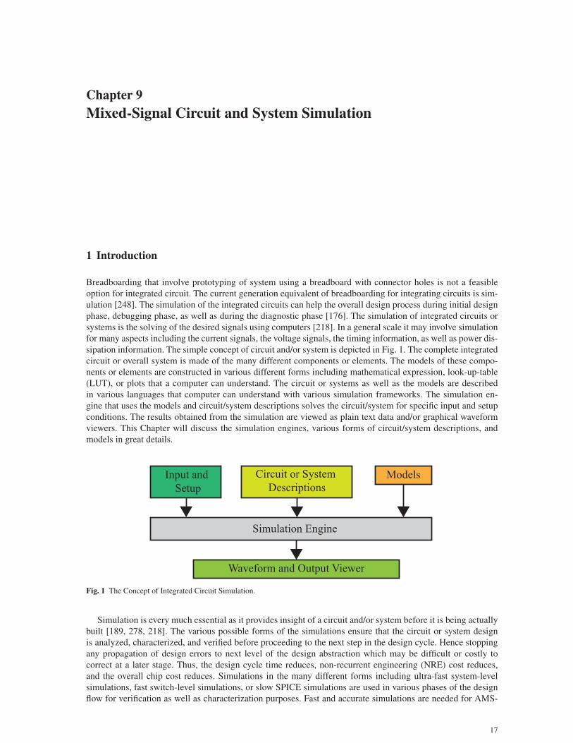
Chapter 9Mixed-Signal Circuit and System Simulation
1 Introduction
Breadboarding that involve prototyping of system using a breadboard with connector holes is not a feasible
option for integrated circuit. The current generation equivalent of breadboarding for integrating circuits is sim-
ulation [248]. The simulation of the integrated circuits can help the overall design process during initial design
phase, debugging phase, as well as during the diagnostic phase [176]. The simulation of integrated circuits or
systems is the solving of the desired signals using computers [218]. In a general scale it may involve simulation
for many aspects including the current signals, the voltage signals, the timing information, as well as power dis-
sipation information. The simple concept of circuit and/or system is depicted in Fig. 1. The complete integrated
circuit or overall system is made of the many different components or elements. The models of these compo-
nents or elements are constructed in various different forms including mathematical expression, look-up-table
(LUT), or plots that a computer can understand. The circuit or systems as well as the models are described
in various languages that computer can understand with various simulation frameworks. The simulation en-
gine that uses the models and circuit/system descriptions solves the circuit/system for specific input and setup
conditions. The results obtained from the simulation are viewed as plain text data and/or graphical waveform
viewers. This Chapter will discuss the simulation engines, various forms of circuit/system descriptions, and
models in great details.
Simulation Engine
ModelsCircuit or System Descriptions
Input and Setup
Waveform and Output Viewer
Fig. 1 The Concept of Integrated Circuit Simulation.
Simulation is every much essential as it provides insight of a circuit and/or system before it is being actually
built [189, 278, 218]. The various possible forms of the simulations ensure that the circuit or system design
is analyzed, characterized, and verified before proceeding to the next step in the design cycle. Hence stopping
any propagation of design errors to next level of the design abstraction which may be difficult or costly to
correct at a later stage. Thus, the design cycle time reduces, non-recurrent engineering (NRE) cost reduces,
and the overall chip cost reduces. Simulations in the many different forms including ultra-fast system-level
simulations, fast switch-level simulations, or slow SPICE simulations are used in various phases of the design
flow for verification as well as characterization purposes. Fast and accurate simulations are needed for AMS-
17
103
References
1. Analog and Mixed-Signal Modeling Using the VHDL-AMS Language. http://tams-www.informatik.uni-hamburg.de/vhdl/doc/P1076.1/tutdac99.pdf. Accessed on 05 April 2014
2. Analog Digital Turbo Simulator (ADiT™). http://www.mentor.com/products/ic_nanometer_design/analog-mixed-signal-verification/adit/. Accessed on 26 March 2014
3. Analog FastSPICE™ (AFS). http://www.berkeley-da.com/prod/datasheets/Berkeley_DA_Platform_DS.pdf. Accessed on 27 March 2014
4. B2.Spice A/D Circuit Simulation Software. http://www.5spice.com/. Accessed on 25 March 20145. Cider Mixed-Level Circuit Simulator. http://www-cad.eecs.berkeley.edu/Software/cider.html. Last
Accessed on 26 March 20146. CircuitLogix. https://www.circuitlogix.com/. Accessed on 25 March 20147. CoolSpice. http://coolcadelectronics.com/coolspice/. Accessed on 25 March 20148. CustomSim™. http://www.synopsys.com/Tools/Verification/AMSVerification/
CircuitSimulation/Pages/CustomSim-ds.aspx. Accessed on 26 March 20149. Discovery AMS. http://www.synopsys.com/Tools/Verification/AMSVerification/
AnalogDigital/AMS/Pages/default.aspx. Accessed on 03 April 201410. Eldo® Classic. http://www.mentor.com/products/ic_nanometer_design/
analog-mixed-signal-verification/eldo/. Accessed on 25 March 201411. Eldo® Premier. http://www.mentor.com/products/ic_nanometer_design/
analog-mixed-signal-verification/eldo-premier/. Accessed on 27 March 201412. FineSim™. http://www.synopsys.com/Tools/Verification/AMSVerification/Pages/
finesim-ds.aspx. Accessed on 26 March 201413. General-purpose Semiconducor Simulator (GSS) TCAD for NgSpice. http://ngspice.sourceforge.net/gss.
html. Accessed on 26 March 201414. Genius Device Simulator. http://www.cogenda.com/. Accessed on 26 March 201415. Giga-scale Parallel SPICE Simulator- NanoSpice™. http://www.proplussolutions.com/en/pro2/
Giga-scale-Parallel-SPICE-Simulator---NanoSpice.html. Accessed on 09 March 201416. HSIM™. http://www.synopsys.com/Tools/Verification/AMSVerification/
CircuitSimulation/HSIM/Pages/default.aspx. Accessed on 26 March 201417. HSPICE®. http://www.synopsys.com/Tools/Verification/AMSVerification/
CircuitSimulation/HSPICE/Documents/hspice_ds.pdf. Accessed on 25 March 201418. Incisive Enterprise Simulator. http://www.cadence.com/rl/Resources/datasheets/incisive_
enterprise_specman.pdf. Accessed on 31 March 201419. Introduction to Quartus® II Software. http://www.altera.com/literature/manual/quartus2_
introduction.pdf. Accessed on 31 March 201420. Introduction to VHDL-AMS. http://www.denverpels.org/Downloads/Denver_PELS_20071113_
Cooper_VHDL-AMS.pdf. Accessed on 06 April 201421. IRSIM Version 9.7 Switch-level Simulator. http://opencircuitdesign.com/irsim/. Accessed on 20 March
201422. ISE Simulator (ISim). http://www.xilinx.com/tools/isim.htm. Accessed on 31 March 201423. IsSpice4. http://www.intusoft.com/products/ICAP4Professional.htm. Accessed on 07 April 201424. LTSpice. http://www.linear.com/designtools/software/. Accessed on 26 March 201425. MATLAB Function. http://www.mathworks.com/help/simulink/slref/matlabfunction.html. Ac-
cessed on 23 March 201426. Micro-Cap. http://www.spectrum-soft.com/down/ug11.pdf. Accessed on 25 March 201427. ModelSim™. http://www.mentor.com/products/fpga/model. Accessed on 31 March 201428. Multisim. http://www.ni.com/multisim/. Accessed on 25 March 201429. MyHDL - From Python to Silicon! http://www.myhdl.org/. Accessed on 13 March 201430. Ngspice. http://ngspice.sourceforge.net/. Accessed on 26 March 2014.31. OpenMAST™. http://www.openmast.org/. Last Accessed on 16 March 201432. OpenVera®. http://www.open-vera.com/. Accessed on 20 March 201433. Parallel SmartSpice: Fast and Accurate Circuit Simulation Finally Available. http://www.silvaco.com/tech_
lib_TCAD/simulationstandard/1997/may/a1/a1.html. Accessed on 25 March 201434. PSpice®. http://www.cadence.com/products/orcad/pspice_simulation/pages/default.aspx.
Accessed on 26 March 201435. Questa® ADMS. http://www.mentor.com/products/ic_nanometer_design/
analog-mixed-signal-verification/advance-ms/. Accessed on 03 Apr 201436. Quite Universal Circuit Simulator (Qucs). http://qucs.sourceforge.net/. Accessed on 26 March 201437. Saber®. http://www.synopsys.com/Systems/Saber/Pages/default.aspx38. SIMetrix. http://www.simetrix.co.uk/site/simetrix-classic.html. Accessed on 26 March 201439. SmartSpice™. http://www.silvaco.com/products/analog_mixed_signal/smartspice.html. Ac-
cessed on 26 March 201440. SMASH - Mixed-Signal Simulator. http://www.dolphin.fr/medal/downloads/pdf/smash/Brochure_
SMASH.pdf. Accessed on 26 March 2014
104
41. Solve Elec. http://www.physicsbox.com/indexsolveelec2en.html. Accessed on 26 March 201442. Solver Pane. http://www.mathworks.com/help/simulink/gui/solver-pane.html. Accessed on 24
March 201443. Spectre® Circuit Simulator. http://www.cadence.com/products/cic/spectre_circuit/pages/
default.aspx. Accessed on 26 March 201444. Spectre® eXtensive Partitioning Simulator (Spectre® XPS). http://www.cadence.com/products/cic/
Spectre_eXtensive_Partitioning_Simulator/pages/default.aspx. Accessed on 26 March 201445. SPICE Analysis Fundamentals. http://www.ni.com/white-paper/12794/en/. Accessed on 27 March 201446. Subclassing and Inheritance. http://www.mathworks.com/help/physmod/simscape/lang/
subclassing-and-inheritance.html. Accessed on 25 March 201447. Super-FinSim. http://www.fintronic.com/product_description.html#Super-FinSim. Accessed on
31 March 201448. SymSpice Turbo. http://www.symica.com/technology/fast-spice-technology. Accessed on 27 March
201449. SystemC-AMS. http://www.systemc-ams.org/. Accessed on 17 March 201450. SystemC AMS extensions User’s Guide. http://kona.ee.pitt.edu/socvlsi/lib/exe/fetch.php?
media=osci_systemc_ams_users_guide.pdf. Accessed on 18 March 201451. T-Spice™. http://www.penzar.com/topspice/topspice.htm. Accessed on 26 March 201452. TclSpice. http://qucs.sourceforge.net/. Accessed on 26 March 201453. The Analog, Mixed-Technology and Mixed-Signal HDL for Saber. http://www.synopsys.com/Systems/Saber/
Pages/MAST.aspx54. The Guide to SystemC. https://www.doulos.com/knowhow/systemc/. Accessed on 02 Apr 201455. TINA-TI™. http://www.ti.com/tool/tina-ti. Accessed on 26 March 201456. TINA™. http://www.tina.com/. Accessed on 26 March 201457. TopSpice. http://www.penzar.com/topspice/topspice.htm. Accessed on 26 March 201458. Turbo-MSIM. http://www.legenddesign.com/products/tbmsim.shtml. Accessed on 26 March 201459. Using Verilog-A to Simplify a SPICE Netlist. http://www.silvaco.com/content/appNotes/analog/
1-004_Verilog-A.pdf. Accessed on 12 March 201460. VCS : Functional Verification Choice of Leading SoC Design Teams. http://www.synopsys.com/Tools/
Verification/FunctionalVerification/Documents/vcs-ds.pdf. Accessed on 31 March 201461. Verilog HDL: Behavioral Counter. http://www.altera.com/support/examples/exm-index.html. Ac-
cessed on 13 March 201462. VHDL-AMS Introduction. http://www.dolphin.fr/projects/macros/dissemination/pdf/
tutorial_vhdl_ams.pdf. Accessed on 05 April 201463. Virtuoso® AMS Designer. http://www.cadence.com/products/cic/ams_designer/pages/default.
aspx. Accessed on 03 Apr 201464. Virtuoso® UltraSim Full-Chip Simulator. http://www.cadence.com/products/cic/UltraSim_fullchip/
pages/default.aspx. Accessed on 26 March 201465. What Is the Simscape Language? http://www.mathworks.com/help/physmod/simscape/lang/
what-is-the-simscape-language.html. Accessed on 25 March 201466. Winspice. http://www.winspice.com/. Accessed on 26 March 201467. XSPICE. http://users.ece.gatech.edu/mrichard/Xspice/. Accessed on 26 March 201468. IEEE Standard VHDL Language Reference Manual. ANSI/IEEE Std 1076-1993 (1994). DOI 10.1109/IEEESTD.1994.
12143369. Parallel SmartSpice: Fast and Accurate Circuit Simulation Finally Available. Simulation Standard 8(5), 1–11 (1997). Ac-
cessed on 25 March 201470. IEEE Standard VHDL Analog and Mixed-Signal Extensions. IEEE Std 1076.1-1999 (1999). DOI 10.1109/IEEESTD.1999.
9057871. The Gnu Circuit Analysis Package, User’s manual. http://www.gnu.org/software/gnucap/man/index.
html (2002). Accessed on 26 March 201472. Behavioral Modeling of PLL Using Verilog-A. http://www.silvaco.com/tech_lib_TCAD/
simulationstandard/2003/jul/a2/july2003_a2.pdf (2003). Accessed on 15 March 201473. Using Hierarchy and Isomorphism To Accelerate Circuit Simulation. Tech. rep., Cadence Design Systems, Inc., San Jose,
CA 95134 USA (2004). Accessed on 06 March 2014.74. Paramos: A Process-Dependent Compact SPICE Model Extractor. http://www.synopsys.com/Tools/TCAD/
CapsuleModule/news_dec06.pdf (2006). Accessed on 08 April 201475. GNU General Public License (GPL). http://www.gnu.org/copyleft/gpl.html (2007). Accessed on 21 March
201476. IEEE Standard VHDL Analog and Mixed-Signal Extensions. IEEE Std 1076.1-2007 (Revision of IEEE Std 1076.1-1999)
pp. c1–328 (2007). DOI 10.1109/IEEESTD.2007.438430977. HSPICE® User Guide: Simulation and Analysis. http://cseweb.ucsd.edu/classes/wi10/cse241a/
assign/hspice_sa.pdf (2008). Accessed on 11 Mar 201478. IEEE Standard VHDL Language Reference Manual - Redline. IEEE Std 1076-2008 (Revision of IEEE Std 1076-2002) -
Redline pp. 1–620 (2009)79. Engineering Education and Research Using MATLAB, chap. Mixed-Signal Circuits Modelling and Simulations Using MAT-
LAB. InTech (2011). DOI 10.5772/21556. Accessed on 28 Feb 2014
105
80. Scicos: Block Diagram Modeler/Simulator. http://www.scicos.org/ (2011). Accessed on 23 March 201481. VHDL Code for a Simple ALU. http://vhdlguru.blogspot.com/2011/06/
vhdl-code-for-simple-alu.html (2011). Accessed on 13 March 201482. BSIM Group. http://www-device.eecs.berkeley.edu/bsim/ (2012). Accessed on 08 April 201483. HiSIM: Hi-Roshima University STARC IGFET Model. http://www.hisim.hiroshima-u.ac.jp/ (2012). Ac-
cessed on 08 April 201484. Block Libraries. http://www.mathworks.com/help/simulink/block-libraries.html (2013). Accessed
on 01 March 201485. BSIM6.0 MOSFET Compact Model. http://www-device.eecs.berkeley.edu/bsim/Files/BSIM6/
BSIM6.0.0/BSIM6.0.0_Technical_manual.pdf (2013). Accessed on 08 April 201486. BeagleBone. http://beagleboard.org/ (2014). Accessed on 23 March 201487. GNU Octave. https://www.gnu.org/software/octave/ (2014). Accessed on 21 March 201488. HDL Coder™. http://www.mathworks.com/products/hdl-coder/ (2014). Accessed on 23 March 201489. KSpice. http://embedded.eecs.berkeley.edu/pubs/downloads/spice/kspice.html (2014). Ac-
cessed on 26 March 201490. LabVIEW System Design Software. http://www.ni.com/labview/ (2014). Accessed on 23 March 201491. MapleSim. http://www.maplesoft.com/products/maplesim/ (2014). Accessed on 23 March 201492. MATLAB® : The Language of Technical Computing. http://www.mathworks.com/products/matlab/ (2014).
Accessed on 20 March 201493. Mystic Statistical Compact Model Extractor. http://www.goldstandardsimulations.com/products/
mystic/ (2014). Accessed on 08 April 201494. Raspberry Pi. http://www.raspberrypi.org/ (2014). Accessed on 23 March 201495. Scilab. http://www.scilab.org/ (2014). Accessed on 21 March 201496. SciPy. http://www.scipy.org/ (2014). Accessed on 21 March 201497. SimRF™. http://www.mathworks.com/products/simrf/ (2014). Accessed on 23 March 201498. Simscape® : Model and Simulate Multidomain Physical Systems. http://www.mathworks.com/products/
simscape/ (2014). Accessed on 20 March 201499. Simulink® : Simulation and Model-Based Design. http://www.mathworks.com/products/simulink/ (2014).
Accessed on 20 March 2014100. Simulink® User’s Guide. http://www.mathworks.com/help/releases/R2014a/pdf_doc/simulink/
sl_using.pdf (2014). Accessed on 23 March 2014101. VisSim™. http://www.vissim.com/ (2014). Accessed on 23 March 2014102. Accelera International, Inc.: SystemC Version 2.0 Users Guide (2002). Accessed on 14 Mar 2014103. Accelera International, Inc.: SystemVerilog 3.1a Language Reference Manual (2004). Accessed on 13 Mar 2014104. Accelera International, Inc.: Verilog-AMS Language Reference Manual: Analog & Mixed-Signal Extensions to Verilog-HDL
(2009). Accessed on 12 Mar 2014105. Adzmi, A., Nasrudin, A., Abdullah, W., Herman, S.: Memristor Spice model for designing analog circuit. In: Proceedings of
the IEEE Student Conference on Research and Development (SCOReD), pp. 78–83 (2012). DOI 10.1109/SCOReD.2012.6518615
106. Agu, E., Mohanty, S.P., Kougianos, E., Gautam, M.: Simscape Based Design Flow for Memristor Based ProgrammableOscillators. In: Proceedings of the 23rd ACM/IEEE Great Lakes Symposium on VLSI (2014)
107. Ahmed, S.I., Kwasniewski, T.A.: A Multiple-Rotating-Clock-Phase Architecture for Digital Data Recovery Circuits usingVerilog-A. In: Proceedings of the 2005 IEEE International Behavioral Modeling and Simulation Workshop, pp. 112–117(2005)
108. Al-Junaid, H., Kazmierski, T.: Analogue and Mixed-Signal Extension to SystemC. IEE Proceedings - Circuits, Devices andSystems pp. 682–690 (2005). DOI doi:10.1049/ip-cds:20045204
109. Ale, A.K.: Comparison and Evaluation of Existing Analog Circuit Simulators Using a Sigma-Delta Modulator. Master’sthesis, Computer Science and Egnineering, University of North Texas, Denton, TX, USA (2006)
110. Andresen, R.P.: 5Spice Analysis Software. http://www.5spice.com/. Accessed on 25 March 2014111. andJeremyPaatela andGuenterDannoritzer andScottHussong, T.: AcceleratingAlgorithmImplementationinF-
PGA/ASICUsingPython. http://www.ll.mit.edu/HPEC/agendas/proc07/Day2/12_Dillon_Poster.pdf. Accessed on 21 March 2014
112. andJeremyPaatela andGuenterDannoritzer andScottHussong, T.: AcceleratingAlgorithmImplementationinF-PGA/ASICUsingPython. In: Proceedings of the High Performance Embedded Computing Workshop (2007). Accessed on13 Mar 2014
113. Ashari, Z.M., Nordin, A.N., Ibrahimy, M.I.: Design of a 5GHz Phase-Locked Loop. In: Proceedings of the IEEE RegionalSymposium on Micro and Nanoelectronics (RSM), pp. 167–171 (2011). DOI 10.1109/RSM.2011.6088316
114. Ashenden, P.J.: The Student’s Guide to VHDL. Morgan Kaufmann. Elsevier Science & Technology Books (2008). URLhttp://books.google.com/books?id=iskV16bpYdgC
115. Ashenden, P.J., Peterson, G.D., Teegarden, D.A.: The System Designer’s Guide to VHDL-AMS: Analog, Mixed-Signal,and Mixed-Technology Modeling. Systems on Silicon. Elsevier Science (2002). URL http://books.google.com/books?id=bvL-sspwj68C
116. Attia, J.O.: Electronics and Circuit Analysis Using MATLAB, second edition edn. MATLAB Series. Taylor & Francis(2004). URL http://books.google.com/books?id=UHr1XPrIRxIC
117. Bailey, S.: Comparison of VHDL, Verilog and SystemVerilog. http://www.fpga.com.cn/advance/vhdl_14919.pdf. Accessed on 13 March 2014

106
118. Banerjee, A., Sur, B.: Systemc and Systemc-AMS in Practice. Springer Verlag (2013). URL http://books.google.com/books?id=yppXnQEACAAJ
119. Banerjee, D.: PLL Performance, Simulation and Design. Dog Ear Publishing (2006). URL http://books.google.com/books?id=R7fZVrIeyJcC
120. Barnasconi, M.: Introduction to SystemC AMS. http://www.iscug.in/sites/default/files/ISCUG-2013/ppt/day1/1_4_3_Introduction_SystemC_AMS_March2013.pdf (2013). Accessed on18 March 2014
121. Berman, V.: A Tale Of Two Languages: SystemC and SystemVerilog. http://chipdesignmag.com/display.php?articleId=116. Accessed on 14 March 2014
122. Bernstein, H.: Understanding the SPICE Simulation Engine. DESIGN SOLUTIONS 1, 9–10 (2003). Accessed on 10 March2014
123. Berny, A.D., Meyer, R.G., Niknejad, A.: Analysis and Design of Wideband LC VCOs. Ph.D. thesis, EECS Department,University of California, Berkeley (2006). URL http://www.eecs.berkeley.edu/Pubs/TechRpts/2006/EECS-2006-50.html
124. Bhasker, J.: A SystemC Primer. Star Galaxy Publishing (2004). URL http://books.google.com/books?id=OpidAAAACAAJ
125. Biolek, D., Biolek, Z., Biolkova, V.: SPICE Modeling of Memristive, Memcapacitative and Meminductive Systems. In:Proceedings of the European Conference on Circuit Theory and Design, pp. 249–252 (2009)
126. Biolek, Z., Biolek, D., Biolkova, V.: SPICE Model of Memristor with Nonlinear Dopant Drift. Radioengineering 18(2),210–214 (2009)
127. Bjørnsen, J., Ytterdal, T.: Behavioral Modeling and Simulation of High Speed Analog-to-Digital Converters using SystemC.In: Proceedings of the International Symposium on Circuits and Systems, pp. 906–909 (2003)
128. Brown, A.D., Zwolinski, M.: The Continuous-Discrete Interface - What does this Really Mean? In: Proceedings of theInternational Symposium on Circuits and Systems, pp. 894–897 (2003)
129. Brown, S.D., Brown, S., Vranesic, Z.: Fundamentals of Digital Logic with VHDL Design. McGraw-Hill Series in Elec-trical and Computer Engineering Series. McGraw-Hill Higher Education (2004). URL http://books.google.com/books?id=Oygh3IDUTgsC
130. Cai, W.: FPGA Prototyping of A Watermarking Algorithm. Master’s thesis, Electrical Egnineering Technology, Universityof North Texas, Denton, TX, USA (2006)
131. Chang, H., Kundert, K.: Verification of Complex Analog and RF IC Designs. Proceedings of the IEEE 95(3), 622–639(2007). DOI 10.1109/JPROC.2006.889384
132. Chaudhary, V., Francis, M., Huang, X., Mantooth, H.A.: Paragon - A Mixed-Signal Behavioral Modeling Environment.In: Proceedings of the International Conference on Communications, Circuits and Systems and West Sino Expositions, pp.1315–1321 (2002). DOI 10.1109/ICCCAS.2002.1179024
133. Chen, G.: A Short Historical Survey of Functional Hardware Languages. ISRN Electronics 2012(271836), 11 pages (2012).DOI 10.5402/2012/271836. Accessed on 21 march 2014
134. Chen, X., Wang, Y., Yang, H.: An Adaptive LU Factorization Algorithm For Parallel Circuit Simulation. In: Proceedings ofthe 17th Asia and South Pacific Design Automation Conference (ASP-DAC), pp. 359–364 (2012). DOI 10.1109/ASPDAC.2012.6164974
135. Christen, E., Bakalar, K.: VHDL-AMS – A Hardware Description Language for Analog and Mixed-Signal Applications.IEEE Trans. on Circuits and Systems – II: Analog and Digital Signal Processing 46(10), 1263–1272 (1999)
136. Cooper, R.S.: The Designer’s Guide to Analog & Mixed-Signal Modeling: Illustrated with VHDL-AMS and MAST. http://www.openmast.com (2004). Accessed on 16 March 2014
137. da Costa, H.J.B., de Assis Brito Filho, F., de Araujo do Nascimento, P.I.: Memristor Behavioural Modeling and SimulationsUsing Verilog-AMS. In: Proceedings of the IEEE Third Latin American Symposium on Circuits and Systems (LASCAS),pp. 1–4 (2012). DOI 10.1109/LASCAS.2012.6180334
138. Cox F. L., I., Kuhn, W.B., Murray, J.P., Tynor, S.D.: Code-Level Modeling in XSPICE. In: Proceedings of the IEEE Interna-tional Symposium on Circuits and Systems, vol. 2, pp. 871–874 (1992). DOI 10.1109/ISCAS.1992.230083
139. Davis, A.T.: Implicit Mixed-Mode Simulation of VLSI Circuits. Ph.D. thesis, Department of Electrical Engineering, Collegeof Engineering and Applied Science, University of Rochester, Rochester, New York (1991). Accessed on 18 March 2014
140. Decaluwe, J.: MyHDL Manual (2013). Accessed on 12 Mar 2014141. Depeyrot, G., Poullet, F., Dumas, B.: Verilog-A Compact Model Coding Whitepaper. In: Proceedings of the Nanotech, pp.
821–824. Anaheim, CA, USA (2010). Accessed on 29 March 2014.142. Dunga, M.V.: Nanoscale CMOS Modeling. Ph.D. thesis, EECS Department, University of California, Berkeley (2008).
Accessed on 19 March 2014143. Dutton, R.W., Strojwas, A.J.: Perspectives on Technology and Technology-Driven CAD. IEEE Transactions on Computer-
Aided Design of Integrated Circuits and Systems 19(12), 1544–1560 (2000). DOI 10.1109/43.898831144. Eidsness, C.: eispice. http://www.thedigitalmachine.net/eispice.html. Accessed on 26 March 2014145. Enz, C., Krummenacher, F., Vittoz, E.: An Analytical MOS Transistor Model Valid in All Regions of Operation and Ded-
icated To Low-voltage and Low-Current Applications. Journal on Analog Integrated Circuits and Signal Processsing 8,83–114 (1995)
146. Eshraghian, K., Kavehei, O., Cho, K.R., Chappell, J.M., Iqbal, A., Al-Sarawi, S.F., Abbott, D.: Memristive Device Fun-damentals and Modeling: Applications to Circuits and Systems Simulation. Proceedings of the IEEE 100(6), 1991–2007(2012). DOI 10.1109/JPROC.2012.2188770
147. Fitzpatrick, D.: Analog Design and Simulation Using OrCAD Capture and PSpice. Newnes (2011). URL http://books.google.com/books?id=7feFVDFzGPQC
107
148. Foty, D.: Mosfet modeling for circuit simulation. IEEE Circuits and Devices Magazine 14(4), 26–31 (1998). DOI 10.1109/101.708477
149. Foty, D., Foty, D.P.: MOSFET Modeling With SPICE: Principles and Practice. Prentice Hall series in innovative technology.Prentice Hall PTR (1997). URL http://books.google.com/books?id=tSVTAAAAMAAJ
150. Frey, P., O’Riordan, D.: Verilog-AMS: Mixed-Signal Simulation and Cross Domain Connect Modules. In: IEEE/ACMInternational Workshop on Behavioral Modeling and Simulation, pp. 103–108 (2000)
151. Garitselov, O.: Metamodeling-Based Fast Optimization Of Nanoscale AMS-SoCs. Ph.D. thesis, Computer Science andEngineering, University Of North Texas, Denton, 76203, TX, USA (2012)
152. Garitselov, O., Mohanty, S., Kougianos, E.: A Comparative Study of Metamodels for Fast and Accurate Simulation of Nano-CMOS Circuits. Semiconductor Manufacturing, IEEE Transactions on 25(1), 26–36 (2012). DOI 10.1109/TSM.2011.2173957
153. Gautam, M.: Exploring Memristor Based Analog Design in Simscape. Master’s thesis, Computer Science and Egnineering,University of North Texas, Denton, TX, USA (2006)
154. Gerfers, F., Ortmanns, M.: Continuous-Time Sigma-Delta A/D Conversion: Fundamentals, Performance Limits and RobustImplementations, 1 edn. Springer (2005)
155. Ghai, D.: Variability Aware Low-Power Techniques for Nanoscale Mixed-Signal Circuits. Ph.D. thesis, Computer Scienceand Engineering, University of North Texas, Denton, TX 76203, USA. (2009)
156. Gielen, G., Wambacq, P., Sansen, W.M.: Symbolic Analysis Methods and Applications For Analog Circuits: A TutorialOverview. Proceedings of the IEEE 82(2), 287–304 (1994). DOI 10.1109/5.265355
157. Gopinath, A.: What’s New in SPICE. Electronics For You pp. 107–109 (2013). Accessed on 25 March 2014158. de Graaf, A.: SystemC-AMS Analog & Mixed-Signal System Design. http://ens.ewi.tudelft.nl/Education/
courses/et4351/SystemC-AMS-2011v2.pdf (2011). Accessed on 18 March 2014159. Grout, I.A., Keane, K.: A MATLAB to VHDL Conversion Toolbox for Digital Control. In: Proceedings of the IFAC Sym-
posium on Computer Aided Control Systems Design (2000)160. Gu, B., Gullapalli, K.K., Hamm, S., Mulvaney, B.: Implementing Nonlinear Oscillator Macromodels using Verilog-AMS
for Accurate Prediction of Injection Locking Behaviors of Oscillators. In: Proceedings of the IEEE International BehavioralModeling and Simulation Workshop, pp. 43–47 (2005)
161. Guan, X.H., Zhang, M.M., Zheng, Y.: MATLAB Simulation in Signals & Systems Using MATLAB at Different Levels.In: Proceedings of the First International Workshop on Education Technology and Computer Science, pp. 952–955 (2009).DOI 10.1109/ETCS.2009.476
162. Guihal, D., Andrieux, L., Esteve, D., Cazarre, A.: VHDL-AMS Model Creation. In: Proceedings of the International Con-ference Mixed Design of Integrated Circuits and System, pp. 549–554 (2006). DOI 10.1109/MIXDES.2006.1706640
163. Gupta, S., Krogh, B., Rutenbar, R.A.: Towards Formal Verification of Analog Designs. In: Proceedings of the IEEE/ACMInternational Conference on Computer Aided Design, pp. 210–217 (2004). DOI 10.1109/ICCAD.2004.1382573
164. Han, L., Zhao, X., Feng, Z.: TinySPICE: A Parallel SPICE Simulator on GPU for Massively Repeated Small Circuit Simu-lations. In: Proceedings of the Design Automation Conference (DAC), pp. 1–8 (2013)
165. Harasymiv, I., Dietrich, M., Knochel, U.: Fast Mixed-Mode PLL Simulation Using Behavioral Baseband Models Of Voltage-Controlled Oscillators and Frequency Dividers. In: Proceedings of the XIth International Workshop on Symbolic and Nu-merical Methods, Modeling and Applications to Circuit Design (SM2ACD), pp. 1–6 (2010). DOI 10.1109/SM2ACD.2010.5672294
166. Hewlett, J.D., Wilamowski, B.M.: SPICE as a Fast and Stable Tool for Simulating a Wide Range of Dynamic Systems.International Journal of Engineering Education 27(2), 217–224 (2011). Accessed on 10 March 2014
167. Iman, S., Joshi, S.: The e-Hardware Verification Language. Springer (2004). URL http://books.google.com/books?id=Zqqy\_bulKogC
168. Jahn, S., Margraf, M., Habchi, V., Jacob, R.: Quite Universal Circuit Simulator (Qucs). http://www.thedigitalmachine.net/reference/QUCS_White_Paper.pdf (2005). Accessed on 09 March 2014
169. Johansson, H., Frisk, J., Drejfert, A.: pycircuit. http://docs.pycircuit.org/. Accessed on 26 March 2014170. Johns, D.A.: The SPICE Circuit Simulator. http://www.eecg.toronto.edu/˜johns/spice/spice_manual.
html. Accessed on 05 March 2014171. Kapre, N.: SPICE2 – A Spatial Parallel Architecture for Accelerating the SPICE Circuit Simulator. Ph.D. thesis, California
Institute of Technology, Pasadena, California (2010). Last Accessed on 04 March 2014172. Kapre, N., DeHon, A.: Accelerating SPICE Model-Evaluation using FPGAs. In: Proceedings of the 17th IEEE Symposium
on Field Programmable Custom Computing Machines, pp. 37–44 (2009). DOI 10.1109/FCCM.2009.14173. Kazmierski, T.: Phase-Locked Loop Frequency Multiplier. http://www.syssim.ecs.soton.ac.uk/vhdl-ams/
examples/pll.htm (1997). Accessed on 15 March 2014174. Kazmierski, T.: VCO with Phase Integration. http://www.syssim.ecs.soton.ac.uk/vhdl-ams/examples/
vco.htm (1997). Accessed on 15 March 2014175. Khan, A., Mohanty, S.P., Kougianos, E.: Statistical Process Variation Analysis of a Graphene FET based LC-VCO for WLAN
Applications. In: Proceedings of the 15th IEEE International Symposium on Quality Electronic Design, pp. 569–574 (2014)176. Kielkowski, R.M.: Inside SPICE: Overcoming the Obstacles of Circuit Simulation. v. 1. McGraw-Hill (1994). URL http:
//books.google.com/books?id=d-VSAAAAMAAJ177. Kougianos, E., Mohanty, S.P.: Impact of Gate-Oxide Tunneling on Mixed-Signal Design and Simulation of a nano-CMOS
VCO. Microelectronics Journal 40(1), 95–103 (2009)178. Kougianos, E., Mohanty, S.P., Pradhan, D.K.: Simulink Based Architecture Prototyping of Compressed Domain MPEG-4
Watermarking. Proceedings of the 12th IEEE International Conference on Information Technology (ICIT) pp. 10–16 (2009)
108
179. Kundert, K.: The Designer’s Guide to SPICE and Spectre®. The Designer’s Guide Book Series. Springer (1995). URLhttp://books.google.com/books?id=bBWS6R\_TEqkC
180. Kundert, K., Zinke, O.: The Designer’s Guide to Verilog-AMS. The Designer’s Guide Book Series. Springer (2004). URLhttp://books.google.com/books?id=DHCgufsJpS0C
181. Lallement, C., Francois Pecheux, A.V., Pregaldiny, F.: Transistor Level Modeling for Analog/RF IC Design, chap. CompactModeling of The MOSFET in VHDL-AMS. Springer (2006)
182. Lemaitre, L., Grabinski, W., Mcandrew, C.: Compact Device Modeling using Verilog-AMS and ADMS. Electron Technology- Internet Journal 35(3), 1–5 (2003). Accessed on 19 March 2014
183. Lemaitre, L., McAndrew, C.: An Open-source Software Tool For Compact Modeling Applications. IEEE Circuits andDevices Magazine 20(2), 6–41 (2004). DOI 10.1109/MCD.2004.1276164
184. Li, R., Zhou, R., Li, G., He, W., Zhang, X., Koo, T.: A Prototype of Model-Based Design Tool and Its Application inthe Development Process of Electronic Control Unit. In: Proceedings of the IEEE 35th Annual Computer Software andApplications Conference Workshops (COMPSACW), pp. 236–242 (2011). DOI 10.1109/COMPSACW.2011.50
185. Liyi, X., Bin, L., Yizheng, Y., Guoyong, H., Jinjun, G., Peng, Z.: A Mixed-Signal Simulator for VHDL-AMS. In: Proceedingsof the Asia and South Pacific Design Automation Conference, pp. 287–294 (2001)
186. Lu, D.: Compact Models for Future Generation CMOS. Ph.D. thesis, EECS Department, University of California, Berkeley(2011). Accessed on 19 March 2014
187. Lu, J.: Analysis and Design Of 5GHz Phase Locked Loops. In: Proceedings of the 7th International Conference on Solid-State and Integrated Circuits Technology, pp. 1488–1491 (2004). DOI 10.1109/ICSICT.2004.1436886
188. Ma, K., Van Leuken, R., Vidojkovic, M., Romme, J., Rampu, S., Pflug, H., Huang, L., Dolmans, G.: A Fast and AccurateSystemC-AMS Model for PLL. In: Proceedings of the 18th International Conference Mixed Design of Integrated Circuitsand Systems, pp. 411–416 (2011)
189. Maas, S.: Historical Trends and Evolution of Circuit-Simulation Technology. In: Proceedings of the IEEE MTT-S Interna-tional Microwave Symposium, pp. 968–971 (2010). DOI 10.1109/MWSYM.2010.5518025
190. Maiti, T.K., Maiti, C.K.: Nanowires, chap. Technology CAD of Nanowire FinFETs. 978-953-7619-79-4. InTech (2010).DOI 10.5772/39522. Accessed on 19 March 2014
191. Martin, G.: SystemC and the Future of Design Languages: Opportunities for Users and Research. In: Proceedings of the16th Symposium on Integrated Circuits and Systems, pp. 61–62 (2003)
192. McDonald, C.B., Bryant, R.E.: CMOS Circuit Verification With Symbolic Switch-Level Timing Simulation. IEEE Transac-tions on Computer-Aided Design of Integrated Circuits and Systems 20(3), 458–474 (2001). DOI 10.1109/43.913762
193. Meric, I., Han, M.Y., Young, A.F., Ozyilmaz, B., Kim, P., Shepard, K.L.: Current saturation in zero-bandgap, top-gatedgraphene field effect transistors. Nature Nanotechnology 3, 654–659 (2008)
194. Miller, I.: Verilog-A and Verilog-AMS Provides a New Dimension in Modeling and Simulation. In: Proceedings of the ThirdIEEE International Caracas Conference on Devices, Circuits and Systems, pp. C49/1–C49/6 (2000)
195. Mohanty, S.P.: SPICE. http://www.cse.unt.edu/˜smohanty/Teaching/2010Fall_AVS/AVS7_SPICE.pdf. Accessed on 27 March 2014
196. Mohanty, S.P.: Energy and Transient Power Minimization during Behavioral Synthesis. Ph.D. thesis, Department of Com-puter Science and Engineering, University of South Florida, Tampa, USA (2003)
197. Mohanty, S.P.: ISWAR: An Imaging System with Watermarking and Attack Resilience. CoRR abs/1205.4489 (2012)198. Mohanty, S.P.: Memristor: From Basics to Deployment. IEEE Potentials pp. 34–39 (2013)199. Mohanty, S.P., Bhargava, B.K.: Invisible Watermarking Based on Creation and Robust Insertion-Extraction of Image Adap-
tive Watermarks. ACM Transactions on Multimedia Computing, Communications, and Applications 5(2) (2008)200. Mohanty, S.P., Kougianos, E.: Impact of Gate Leakage on Mixed Signal Design and Simulation of Nano-CMOS Circuits.
In: Proceedings of the 13th NASA Symposium on VLSI Design, vol. paper # 2.4, 6 pages (2007)201. Mohanty, S.P., Kougianos, E.: Real-Time Perceptual Watermarking Architectures for Video Broadcasting. Journal of Systems
and Software 84(5), 724–738 (2011)202. Mohanty, S.P., Kougianos, E.: Models, Methods, and Tools for Complex Chip Design: Selected Contributions from FDL
2012, chap. Polynomial Metamodel-Based Fast Optimization of Nanoscale PLL Components. 978-3-319-01417-3. Springer(2014)
203. Mohanty, S.P., Kougianos, E.: Polynomial Metamodel Based Fast Optimization of Nano-CMOS Oscillator Circuits. AnalogIntegrated Circuits and Signal Processing 79(3), 437–453 (2014). DOI 10.1007/s10470-014-0284-2. URL http://dx.doi.org/10.1007/s10470-014-0284-2
204. Mohanty, S.P., Ranganathan, N., Balakrishnan, K.: A Dual Voltage-Frequency VLSI Chip for Image Watermarking in DCTDomain. IEEE Transactions on Circuits and Systems II 53(5), 394–398 (2006). DOI 10.1109/TCSII.2006.870216
205. Mohanty, S.P., Ranganathan, N., Krishna, V.: Datapath Scheduling using Dynamic Frequency Clocking. In: Proceedings ofthe IEEE Computer Society Annual Symposium on VLSI, pp. 65–70 (2002)
206. Moondanos, J.: SystemC Tutorial. http://embedded.eecs.berkeley.edu/research/hsc/class/ee249/lectures/l10-SystemC.pdf. Accessed on 14 March 2014
207. Moore, H.: MATLAB® for Engineers. Always learning. Pearson (2013). URL http://books.google.com/books?id=P7YJngEACAAJ
208. Mysore, O.: Compact Modeling of Circuits and Devices in Verilog-A. Master’s thesis, Department of Electrical Engineeringand Computer Science, Massachusetts Institute of Technology, MA, USA (2012)
209. Nagel, L.W.: SPICE2: A Computer Program to Simulate Semiconductor Circuits. Tech. Rep. ERL-M520, Electronics Re-search Laboratory, College of Engineering, University of California, Berkeley, CA 94720, USA (1975). Accessed on 07March 2014.
109
210. Nagel, L.W.: The Life of SPICE. http://bear.ces.cwru.edu/eecs_cad/cad_spice_history_nagel.html (1996). Accessed on 25 March 2014
211. Nagel, L.W.: Is It Time for SPICE4? In: Numerical Aspects of Circuit Device Modeling Workshop (2004). Accessed on 05March 2014
212. Nagel, L.W., Pederson, D.O.: Simulation Program with Integrated Circuit Emphasis (SPICE). Tech. Rep. ERL-M382, Elec-tronics Research Laboratory, College of Engineering, University of California, Berkeley, CA 94720, USA (1973). Accessedon 05 March 2014.
213. Nance, R.E.: A Histroy of Discrete Event Simulation Programming Languages. Tech. Rep. TR 93-21, Department of Com-puter Science, Virginia Polytechnic Institute and State University, Blacksburg, Virginia 24061, USA (1993). Accessed on 03March 2014
214. Narayanan, R., Abbasi, N., Zaki, M., Al Sammane, G., Tahar, S.: On the Simulation Performance of Contemporary AMSHardware Description Languages. In: Proceedings of the International Conference on Microelectronics, pp. 361–364 (2008).DOI 10.1109/ICM.2008.5393509
215. Neira, H.G.: Electronics Mixed-Mode Simulation. Tech. Rep. ARFSD-TR-93009, U.S. Army Armament Research, Devel-opment and Engineering Center, Fire Support Armaments Center, Picatinny Arsenal, New Jersey (1993). Accessed on 18March 2014.
216. Nenzi, P., Vogt, H.: Ngspice Users Manual: Version 26plus. Tech. rep. (2014). Accessed on 08 March 2014.217. Nikam, S.D.: A Comparison of Software Engines For Simulation of Closed-Loop Control Systems. Master’s thesis, Depart-
ment of Electrical and Computer Engineering, New Jersey Institute of Technology, NJ, USA (2010). Accessed on 23 March2014
218. Ogrodzki, J.: Circuit Simulation Methods and Algorithms. Electronic Engineering Systems. Taylor & Francis (1994). URLhttp://books.google.com/books?id=ybHjM3QH5c4C
219. Okobiah, O.: Exploring Process-Variation Tolerant Design of Nanoscale Sense Amplifier Circuits. Master’s thesis, Depart-ment of Computer Science and Engineering, University of North Texas, Denton, TX (2010)
220. Okobiah, O.: Geostatistical Inspired Metamodeling and Optimization of Nanoscale Analog Circuits. Ph.D. thesis, ComputerScience and Engineering, University Of North Texas, Denton, 76203, TX, USA (2014)
221. Okobiah, O., Mohanty, S.P., Kougianos, E.: Geostatistical-Inspired Fast Layout Optimization of a Nano-CMOS ThermalSensor. IET Circuits, Devices Systems 7(5), 253–262 (2013). DOI 10.1049/iet-cds.2012.0358
222. Okobiah, O., Mohanty, S.P., Kougianos, E., Poolakkaparambil, M.: Towards Robust Nano-CMOS Sense Amplifier Design:A Dual-Threshold Versus Dual-Oxide Perspective. In: Proceedings of the 21st ACM Great Lakes Symposium on VLSI, pp.145–150 (2011)
223. Open Verilog International: Verilog-A Language Reference Manual : Analog Extensions to Verilog HDL (1996). Accessedon 21 Mar 2014
224. Ostroumov, S., Tsiopoulos, L., Sere, K., Plosila, J.: Generation of Structural VHDL Code with Library Components fromFormal Event-B Models. In: Proceedings of the Euromicro Conference on Digital System Design, pp. 111–118 (2013).DOI 10.1109/DSD.2013.20
225. Padmaraju, N.: Analog and Mixed Signal Modeling Approaches. http://www.design-reuse.com/articles/22773/analog-mixed-signal-modeling.html. Accessed on 02 Apr 2014
226. Pavan, S.: Systematic Design Centering of Continuous Time Oversampling Converters. IEEE Transactions on Circuits andSystems II: Express Briefs 57(3), 158–162 (2010). DOI 10.1109/TCSII.2010.2041814
227. Pecheux, F., Lallement, C., Vachoux, A.: VHDL-AMS and Verilog-AMS as Alternative Hardware Description Languagesfor Efficient Modeling of Multidiscipline Systems. IEEE Transactions on Computer-Aided Design of Circuits and Systems24(2), 204–225 (2005)
228. Pershin, Y.V., Di Ventra, M.: Practical Approach to Programmable Analog Circuits With Memristors. IEEE Transactions onCircuits and Systems I 57(8), 1857–1864 (2010)
229. Popescu, G., Goldgeisser, L.: Mixed Signal Aspects Of Behavioral Modeling And Simulation. In: Proceedings of the IEEEInternational Symposium on Circuits and Systems, pp. V–628–V–631 (2004). DOI 10.1109/ISCAS.2004.1329886
230. Prodromakis, T., Peh, B.P., Papavassiliou, C., Toumazou, C.: A Versatile Memristor Model With Nonlinear Dopant Kinetics.IEEE Transactions on Electron Devices 58(9), 3099–3105 (2011)
231. Quarles, T., Newton, A.R., Pederson, D.O., Sangiovanni-Vincentelli, A.: SPICE3 Version 3f3 Users Manual. http://www.physics.ucdavis.edu/Classes/Physics116/SPICE_cp.pdf (1993). Accessed on 11 March 2014
232. Quarles, T.L.: Analysis of Performance and Convergence Issues for Circuit Simulation. Tech. Rep. UCB/ERL M89/42,Electronics Research Laboratory, College of Engineering (1989). Accessed on 04 March 2014
233. Radwan, A.G., Zidan, M.A., Salama, K.N.: On The Mathematical Modeling of Memristors. In: Proceedings of the Interna-tional Conference on Microelectronics, pp. 284–287 (2010). DOI 10.1109/ICM.2010.5696139
234. Rahman, A.B.A.: Modelling of Mixed Physical-Domain System. Master’s thesis, Faculty of Engineering, Science andMathematics, School of Electronics and Computer Science, UK (2010). Accessed on 07 April 2014
235. Ramon, M.E., Parrish, K.N., Chowdhury, S.F., Magnuson, C.W., Movva, H.C.P., Ruoff, R.S., Banerjee, S.K., Akinwande,D.: Three-Gigahertz Graphene Frequency Doubler on Quartz Operating Beyond the Transit Frequency. IEEE Transactionson Nanotechnology 11(5), 877–883 (2012). DOI 10.1109/TNANO.2012.2203826
236. Rewienski, M.: A perspective on fast-spice simulation technology. In: P. Li, L.M. Silveira, P. Feldmann (eds.) Sim-ulation and Verification of Electronic and Biological Systems, pp. 23–42. Springer Netherlands (2011). DOI 10.1007/978-94-007-0149-6 2. URL http://dx.doi.org/10.1007/978-94-007-0149-6_2
237. Rich, D.I.: The Evolution of SystemVverilog. IEEE Design Test of Computers 20(4), 82–84 (2003). DOI 10.1109/MDT.2003.1214355

110
238. Rose, G.S., Rajendran, J., Manem, H., Karri, R., Pino, R.E.: Leveraging Memristive Systems in the Construction of DigitalLogic Circuits. Proceedings of the IEEE 100(6), 2033–2049 (2012)
239. Rowen, C.: Engineering the Complex SOC: Fast, Flexible Design with Configurable Processors. Pearson Education (2008).URL http://books.google.com/books?id=L\_-3Pd5NXm8C
240. Rushton, A.: VHDL for Logic Synthesis. Wiley (2011). URL http://books.google.com/books?id=lC8HKr0e2nwC
241. Sagesaka, H., Irii, H., Asai, H.: SPADE : Analog/Digital Mixed Signal Simulator With Analog Hardware Description Lan-guage. In: Proceedings of the IEEE International Conference on Electronics, Circuits and Systems, pp. 517–520 (1998).DOI 10.1109/ICECS.1998.813375
242. Sah, M.P., Kim, H., Chua, L.O.: Brains Are Made of Memristors. IEEE Circuits and Systems Magazine 14(1), 12–36 (2014).DOI 10.1109/MCAS.2013.2296414
243. Sarivisetti, G.: Design and Optimization of Components in a 45 nm CMOS Phase Locked Loop. Master’s thesis, ComputerScience and Egnineering, University of North Texas, Denton, TX, USA (2006)
244. Schneider, T., Mades, J., Windisch, A., Glesner, M., Monjau, D., Ecker, W.: A System-Level Simulation Environment forSystem-on-Chip Design. In: Proceedings of the 13th Annual IEEE International ASIC/SOC Conference, pp. 58–62 (2000)
245. Schreier, R.: Delta Sigma Toolbox. http://www.mathworks.com/matlabcentral/fileexchange/19-delta-sigma-toolbox (2011). Code covered by the BSD License, Accessed on 01 March 2014.
246. Schreier, R., Temes, G.C.: Understanding Delta-Sigma Data Converters, 1 edn. Wiley-IEEE Press (2004)247. da Silva, A.C.R., Grout, I., Ryan, J., O’Shea, T.: Generating VHDL-AMS Models of Digital-to-Analogue Converters From
MATLAB/SIMULINK. In: Proceedings of the International Conference on Thermal, Mechanical and Multi-Physics Simu-lation Experiments in Microelectronics and Micro-Systems, pp. 1–7 (2007). DOI 10.1109/ESIME.2007.360029
248. Smith, M.J.S.: Application Specific Integrated Circuits. VLSI Systems Series. Addison-Wesley (1997). URL http://books.google.com/books?id=3hxTAAAAMAAJ
249. Steer, M.B.: SPICE: Users Guide and Reference. http://www.freeda.org/doc/SPICE/spice.pdf (2007). Ac-cessed on 11 March 2014
250. Strukov, D.B., Snider, G.S., Stewart, D.R., Williams, R.S.: The Missing Memristor Found. Nature 453(7191), 80–83 (2008)251. Strukov, D.B., Williams, R.S.: Exponential Ionic Drift: Fast Switching and Low Volatility of Thin-Film Memristors. Applied
Physics A: Materials Science & Processing 94(3), 515–519 (2009)252. Suzuki, K., Nishio, A., Kamo, A., Watanabe, T., Asai, H.: An Application of Verilog-A to Meodeling of Back Propagation
Algorithm in Neural Networks. In: Proceedings of the 43rd IEEE Midwest Symposium on Circuits and Systems, pp. 1336–1339 (2000)
253. Tala, D.K.: SystemC Tutorial. http://www.asic-world.com/systemc/tutorial.html (2014). Accessed on13 March 2014
254. Tala, D.K.: SystemVerilog Tutorial. http://www.asic-world.com/systemverilog/tutorial.html (2014).Accessed on 13 March 2014
255. Tan, X.D., Shi, C.J.R.: Hierarchical Symbolic Analysis of Analog Integrated Circuits via Determinant Decision Diagrams.IEEE Transactions On Computer Aided Design of Integrated Circuits and Systems 19(4), 401–412 (2006). DOI 10.1109/43.838990. URL http://dx.doi.org/10.1109/43.838990
256. Trofimov, M., Mosin, S.: The Realization of Algorithmic Description on VHDL-AMS. In: Proceedings of the InternationalConference on Modern Problems of Radio Engineering, Telecommunications and Computer Science, pp. 350–352 (2004)
257. Troyanovsky, B., O’Halloran, P., Mierzwinski, M.: Transistor Level Modeling for Analog/RF IC Design, chap. CompactModeling In Verilog-A. Springer (2006)
258. Tsuboi, K., Okumura, N.: A Next-Generation Workflow for System-Level Design of Mixed-Signal Integrated Circuits. http://www.mathworks.com/tagteam/75539_92085v00_a-next-generation-workflow-for-system-level-design.pdf. Accessed on 28 Feb 2014
259. Uehara, J.: Epson Toyocom Designs and Verifies Mixed-Signal Integrated Cir-cuit in Two Months. http://www.mathworks.com/company/user_stories/Epson-Toyocom-Designs-and-Verifies-Mixed-Signal-Integrated-Circuit-in-Two-Months.html. Accessed on 28 Feb 2014
260. Umoh, I.J., Kazmierski, T.J.: VHDL-AMS Model of A Dual Gate Graphene FET, booktitle = Proceedings of the Forum onSpecification and Design Languages, year = 2011, pages = 1–5,
261. Vachoux, A., Berge, J., Levia, O., Rouillard, J.: Analog and Mixed-Signal Hardware Description Language. Current is-sues in electronic modeling. Kluwer Academic Publishers (1997). URL http://books.google.com/books?id=7i1LAQAAIAAJ
262. Vachoux, A., Grimm, C., Einwich, K.: Towards Analog and Mixed-Signal SoC Design with SystemC-AMS. In: Proceedingsof the IEEE International Conference on Field-Programmable Technology, pp. 97–102 (2004). DOI 10.1109/DELTA.2004.10008
263. Vachoux, A., Grimm, C., Kakerow, R., Meise, C.: Embedded Mixed-Signal Systems: New Challenges For Modeling AndSimulation. In: Proceedings of the IEEE International Symposium on Circuits and Systems, p. 4 pp. (2006). DOI 10.1109/ISCAS.2006.1692754
264. Villar, J.I., Juan, J., Bellido, M.J., Viejo, J., Guerrero, D., Decaluwe, J.: Python As A Hardware Description Language: ACase Study. In: Proceedings of the VII Southern Conference on Programmable Logic, pp. 117–122 (2011). DOI 10.1109/SPL.2011.5782635
265. Vishak, C., Sunil, G.: Phase Locked Loop : Mixed Signal Design Flow. http://www2.ece.ohio-state.edu/
˜bibyk/ece822/VishakandSunilNonThesis.pdf. Accessed on 15 March 2014

111
266. Vladimirescu, A.: THE SPICE BOOK. J. Wiley (1994). URL http://books.google.com/books?id=L-BSAAAAMAAJ
267. Vladimirescu, A.: SPICE-The Fourth Decade Analog and Mixed-signal Simulation - A State Of The Art. In: ProceedingsInternational Semiconductor Conference, pp. 39–44 (1999). DOI 10.1109/SMICND.1999.810383
268. Walsh, A., Carley, R., Feely, O., Ascoli, A.: Memristor Circuit Investigation through a New Tutorial Toolbox. In: Proceedingsof the European Conference on Circuit Theory and Design (ECCTD), pp. 1–4 (2013). DOI 10.1109/ECCTD.2013.6662261
269. Wang, L., Kazmierski, T.J.: VHDL-AMS Based Genetic Optimization of Mixed-Physical-Domain Systems in AutomotiveApplications. Simulation 85(10), 661–670 (2009)
270. Warwick, C.: Everything you always wanted to know about SPICE* *But were afraid to ask. The EMC Journal 82 (2009).Accessed on 04 March 2014
271. Weiqiang, Z., Peimin, W.: PSpice System Simulation Application in Electronic Circuit Design. In: Proceedings of the 32ndChinese Control Conference, pp. 8634–8636 (2013)
272. Wenqing, C., Donglin, S., Derong, C., Chaoxian, Z.: A Behavioral Simulation Method To Predict and Estimate EMi Char-acteristics Of Electronic System. In: Proceedings of the Asia-Pacific Symposium on Electromagnetic Compatibility, pp.742–745 (2008). DOI 10.1109/APEMC.2008.4559982
273. Williams, C.D.H.: MacSpice. http://www.macspice.com/. Accessed on 26 March 2014274. Williams, R.: How We Found The Missing Memristor. IEEE Spectrum 45(12), 28–35 (2008)275. Wong, W., Gao, X., Wang, Y., Vishwanathan, S.: Overview of mixed signal methodology for digital full-chip de-
sign/verification. In: Proceedings of the 7th International Conference on Solid-State and Integrated Circuits Technology,pp. 1421–1424 (2004). DOI 10.1109/ICSICT.2004.1436852
276. Woods, S., Casinovi, G.: Multiple-Level Logic Simulation Algorithm. IEE Proceedings - Computers and Digital Techniques148(3), 129–137 (2001). DOI 10.1049/ip-cdt:20010485
277. Xia, F., Farmer, D.B., Lin, Y.m., Avouris, P.: Graphene Field-Effect Transistors with High On/Off Current Ratio and LargeTransport Band Gap at Room Temperature. Nano Letters 10(2), 715–718 (2010). DOI 10.1021/nl9039636. URL http://pubs.acs.org/doi/abs/10.1021/nl9039636
278. Xiu, L.: VLSI Circuit Design Methodology Demystified: A Conceptual Taxonomy. Wiley (2007). URL http://books.google.com/books?id=69hbACmcZrAC
279. Xu, T., Arriens, H.L., Van Leuken, R., de Graaf, A.: A Precise SystemC-AMS model for Charge Pump Phase Lock Loopwith Multiphase Outputs. In: Proceedings of the IEEE 8th International Conference on ASIC, pp. 50–53 (2009). DOI10.1109/ASICON.2009.5351608
280. Xue, D., Chen, Y.Q.: System Simulation Techniques with MATLAB® and Simulink®. Wiley (2013). URL http://books.google.com/books?id=LYjXAAAAQBAJ
281. Yang, Y., Zhou, S.: A Circuit Simulation Experimental System Based On Re-development SPICE. In: Proceedings of the4th International Congress on Image and Signal Processing, pp. 2531–2535 (2011). DOI 10.1109/CISP.2011.6100711
282. Yerra, T.N.: Design of a Second-Order Delta-Sigma Modulator for Use in Biomedical Signal Acquisition. Master’s thesis,Department of Electrical and Computer Engineering, Southern Illinois University Edwardsville Edwardsville, Illinois, USA(2009). Accessed on 28 Feb 2014
283. Yoder, S.: Timers, Frequency Divider Examples. http://www3.nd.edu/˜cse/2013sp/20221/handouts/L15%20Verilog%20Sequential%20Logic.pdf (2013). Accessed on 15 March 2014
284. Zaidi, Y., Grimm, C., Haase, J.: Fast and Unified SystemC AMS - HDL Simulation. In: Proceedings of the Forum onSpecification Design Languages, pp. 1–6 (2009)
285. Zaplatilek, K.: Memristor Modeling in MATLAB & Simulink. In: Proceedings of the 5th European Conference on EuropeanComputing Conference, pp. 62–67 (2011)
286. Zheng, G.: Layout-Accurate Ultra-Fast System-Level Design Exploration Through Verilog-AMS. Ph.D. thesis, ComputerScience and Engineering, University Of North Texas, Denton, 76203, TX, USA., Denton, TX 76207 (2013)
287. Zheng, G., Mohanty, S.P., Kougianos, E.: Design and Modeling of a Continuous-Time Delta-Sigma Modulator for Biopo-tential Signal Acquisition: Simulink Vs Verilog-AMS Perspective. In: Proceedings of the 3rd International Conference onComputing, Communication and Networking Technologies (2012)
288. Zheng, G., Mohanty, S.P., Kougianos, E., Garitselov, O.: Verilog-AMS-PAM: Verilog-AMS integrated with Parasitic-AwareMetamodels for Ultra-Fast and Layout-Accurate Mixed-Signal Design Exploration. In: Proceedings of the ACM Great LakesSymposium on VLSI, pp. 351–356 (2012)
289. Zheng, G., Mohanty, S.P., Kougianos, E., Okobiah, O.: Polynomial Metamodel Integrated Verilog-AMS for Memristor-BasedMixed-Signal System Design. In: Proceedings of the IEEE 56th International Midwest Symposium on Circuits and Systems(MWSCAS), pp. 916–919. IEEE (2013)
290. Zidan, M.A., Omran, H., Radwan, A.G., Salama, K.N.: Memristor Model. http://sensors.kaust.edu.sa/tools/memristor-model (2011). Code covered by the BSD License, Accessed on 21 Feb 2014.
291. Zidan, M.A., Radwan, A.G., Salama, K.N.: Memristor Model. http://www.mathworks.com/matlabcentral/fileexchange/31530-memristor-model (2011). Code covered by the BSD License, Accessed on 21 Feb 2014.
292. Zorzi, M., Franze, F., Speciale, N.: Construction of VHDL-AMS Simulator in MATLAB. In: Proceedings of the 2003International Workshop on Behavioral Modeling and Simulation, pp. 113–117 (2003)
293. Zorzi, M., Franze, F., Speciale, N., Masetti, G.: A Tool for the Integration of New VHDL-AMS Models in SPICE. In:Proceedings of the 2004 International Symposium on Circuits and Systems, pp. IV–637–IV–640 (2004)
294. Zwolinski, M.: Digital System Design with SystemVerilog. Prentice Hall Signal Integrity Library. Pearson Education (2009).URL http://books.google.com/books?id=wNsgsrNxgPAC
Chapter 10Power, Parasitic, and Thermal Aware AMS-SoC DesignMethodologies
1 Introduction
In a previous Chapter on Design for Excellence (DfX) a large set of issues which are encountered during
the design of nanoelectronic based circuits and systems has been presented. Addresses one or more than one
of these issues are challenging and they demand more efforts from system designer, design engineers, and
layout engineers. The scope of this Chapter is the detailed discussion of a selected subset from DfX which was
discussed in a previous Chapter. In particular, power, parasitics, and thermal issues have been discussed. In
the case of power, static as well dynamic power dissipation have been presented along with their effects and
techniques to handle them at various levels of design abstraction. The parasitics like resistors, capacitors, and
inductors which arise from the active devices as well as passive interconnects can be origin of many problems
such as performance and power dissipation. The parasitics can be distributed and lumped; the distributed are
much more difficult to handle. The parasitics origin, modeling, and methods to handle during design flow
have been presented in this Chapter. Then comes the thermal or temperature issue of the circuits and systems.
The thermal issues are due to high on-chip heating due to high power dissipation or may be high ambient
temperature. The on-chip thermal issues may arise from the high power dissipation. While the power dissipation
issue and thermal issues have some commonalities they are different issues and may been different approaches
to solve them. Therefore, this Chapter discusses the thermal issues as a different issue from power dissipation.
2 Power Dissipation: Remains Key Design Constraint
The research in low-power VLSI design has been one of the primary focus for last several decade [119, 175,
162, 40, 55, 32, 198, 27]. However, it still remains one of the major issues along with the additional emerging
issues in the nanoelectronics era. The explosive growth of portable systems with serious computing capabilities
have been a major driving factor of the low-power design. No doubt, with technology scaling and smaller
feature size the devices are operated at low supply voltages. Hence it can be said the power dissipation of
individual transistors per technology generation reduced. However, the number of transistors which are packed
in the same die i.e. integration density of packing density of the chips increased have increased. It is estimated
that with each generation, feature size has scaled by 0.7, integration density has increased by 2×, cost of
computing reduced by 2×, while die size has minor increase of 14%. Thus the power consumption of the main
stream chip have increased. In the recent years to operate with limited battery life, low-power system-on-a-
chip (SoC) instead of pure hardware main stream microprocessors have been of quite demand. Of course, the
in process the performance has been compromised. One can think why not having high performance battery a
solution! First of all the chemical technology that is used in battery has its own limitations. The size of battery
needed to provide higher current will not be helpful to make portable small electronic systems. In general the
need for high-performance and yet portable small electronic systems and many other factors which are to be
discussed in this Section have kept the power dissipation (including leakage dissipation) as the key constraint
for the design engineers.
19
119
References
1. Hipex Full-Chip Parasitic Extraction. http://www.silvaco.com/content/kbase/hipex_jpws.pdf. Ac-cessed on 09 May 2014
2. Thermally Aware Design Methodology. Tech. rep., Gradient Design Automation Inc. (2005). URLhttp://www.cdnusers.org/community/encounter/resources/resources_imp/route/dtp_cdnlive2005_1349_moynihan.pdf. Accessed on 14th August 2012
3. Taking A Bite Out of Power: Techniques For Low-power-ASIC Design. http://edn.com/Home/PrintView?contentItemId=4314765 (2007). Accessed on 05 May 2014
4. OMAP-Vox™ Single-Chip Solution For Affordable Multimedia-Rich Phones. http://www.ti.com/pdfs/wtbu/TI_omapv1035.pdf (2008). Accessed on 01 May 2014
5. Body Effect and Body Biasing. http://www.suvolta.com/files/2513/0713/0696/BodyEffect_BodyBiasing_TechBrief_Final_6.3.2011.pdf (2011). Accessed on 18 April 2014
6. Building Energy-Efficient ICs from the Ground Up. http://www.cadence.com/rl/Resources/white_papers/low_power_impl_wp.pdf (2011). Accessed on 25 may 2014
7. HotSpot. http://lava.cs.virginia.edu/hotspot/ (2011). Accessed on 26 April 20148. National Semiconductor PowerWise® Adaptive Voltage Scaling Technology. http://www.ti.com/lit/wp/
snvy007/snvy007.pdf (2012). Accessed on 17 April 20149. PowerWise Adaptive Voltage Scaling (AVS). http://www.ti.com/ww/en/analog/power_management/
powerwise-avs.shtml (2014). Accessed on 17 April 201410. Abou-Seido, A.I., Nowak, B., Chu, C.: Fitted Elmore Delay: A Simple and Accurate Interconnect Delay Model. IEEE
Transactions on Very Large Scale Integration (VLSI) Systems 12(7), 691–696 (2004). DOI 10.1109/TVLSI.2004.83093211. Acar, E., Arunachalam, R., Nassif, S.R.: Predicting Short Circuit Power From Timing Models. In: Proceedings of the Asia
and South Pacific Design Automation Conference, pp. 277–282 (2003). DOI 10.1109/ASPDAC.2003.119502912. Agarwal, A.: Algorithms for Layout-Aware and Performance Model Driven Synthesis of Analog Circuits. Ph.D. thesis, De-
partment of Computer Science & Engineering, University of Cincinnati, Ohio (2005). URL http://rave.ohiolink.edu/etdc/view?acc_num=ucin1132259454
13. Akyildiz, I., Su, W., Sankarasubramaniam, Y., Cayirci, E.: A Survey on Sensor Networks. IEEE Communications Magazine40(8), 102–114 (2002). DOI 10.1109/MCOM.2002.1024422
14. Ali, S., Tanner, S., Farine, P.A.: A Robust, Low Power, High Speed Voltage Level Shifter With Built-In Short Circuit CurrentReduction. In: Proceedings of the 20th European Conference on Circuit Theory and Design (ECCTD), pp. 142–145 (2011).DOI 10.1109/ECCTD.2011.6043302
15. Alipour, S., Hidaji, B., Pour, A.S.: Circuit Level, Static Power, and Logic Level Power Analyses. In: Proceedings of theIEEE International Conference on Electro/Information Technology (EIT), pp. 1–4 (2010). DOI 10.1109/EIT.2010.5612180
16. Allstot, D.J., Choi, K., Park, J.: Parasitic-Aware Optimization of CMOS RF Circuits. Springer US (2003). URL http://books.google.com/books?id=l\_ktk67A7GkC
17. Auth, C.: 45nm high-k + metal gate strain-enhanced cmos transistors. In: Proceedings of the IEEE Custom Integrated CircuitsConference, pp. 379–386 (2008). DOI 10.1109/CICC.2008.4672101
18. Badaoui, R.F., Sampath, H., Agarwal, A., Vemuri, R.: A High Level Language For Pre-Layout Extraction in Parasite-AwareAnalog Circuit Synthesis. In: Proceedings of the 14th ACM Great Lakes Symposium on VLSI, pp. 271–276 (2004)
19. Bakker, A., Huijsing, J.H.: High-Accuracy CMOS Smart Temperature Sensors. Series in Engineering and Computer Science.Springer (2000). URL http://books.google.com/books?id=TTw7udu3EqIC
20. Balakrishnan, K.: A Dual Voltage and Dual Frequency Low Power VLSI Implementation of DCT Domain Image Water-marking Schemes. Master’s thesis, Electrical Egnineering Technology, University of South Florida, FL, USA (2003)
21. Ballweber, B.M., Gupta, R., Allstot, D.J.: A fully integrated 0.5− 5.5GHz CMOS distributed amplifier. IEEE Journal ofSolid State Circuits 35(2), 231–239 (2000)
22. Balouchestani, M.: Low-Power Wireless Sensor Network With Compressed Sensing Theory. In: Proceedings of the 4thAnnual Caneus Fly by Wireless Workshop (FBW), pp. 1–4 (2011). DOI 10.1109/FBW.2011.5965565
23. Banerjee, K., Mehrotra, A., Sangiovanni-Vincentelli, A., Hu, C.: On Thermal Effects in Deep Sub-Micron VLSI Intercon-nects. In: Proceedings of the 36th Design Automation Conference, pp. 885–891 (1999). DOI 10.1109/DAC.1999.782207
24. Baschirotto, A., Chironi, V., Cocciolo, G., DAmico, S., De Matteis, M., Delizia, P.: Low Power Analog Design in ScaledTechnologies. In: Proceedings of the Topical Workshop on Electronics for Particle Physics, pp. 103–110 (2009)
25. Bellosa, F., Weißel, A., Waitz, M., Kellner, S.: Event-Driven Energy Accounting for Dynamic Thermal Management. In:Proceedings of the Workshop on Compilers and Operating Systems for Low Power (2003)
26. Bohr, M., Mistry, K.: Intels Revolutionary 22 nm Transistor Technology. http://download.intel.com/newsroom/kits/22nm/pdfs/22nm-details_presentation.pdf (2011). Accessed on 06 may 2014
27. Brodersen, R.W., Chandrakasan, A., Sheng, S.: Technologies For Personal Communications. In: Digest of Technical PapersSymposium on VLSI Circuits, pp. 5–9 (1991). DOI 10.1109/VLSIC.1991.760053
28. Brooks, D., Dick, R.P., Joseph, R., Shang, L.: Power, Thermal, and Reliability Modeling in Nanometer-Scale Microproces-sors. IEEE Micro 27(3), 49–62 (2007). DOI 10.1109/MM.2007.58
29. Brynjolfson, I., Zilic, Z.: Dynamic Clock Management for Low Power Applications in FPGAs. In: Proceedings of the IEEECustom Integrated Circuits Conference, pp. 139–142 (2000)
30. Carroll, A., Heiser, G.: An Analysis Of Power Consumption in a Smartphone. In: Proceedings of the 2010 USENIX AnnualTechnical Conference, pp. 21–21 (2010). URL http://dl.acm.org/citation.cfm?id=1855840.1855861
31. Chan, H., Zilic, Z.: Parasitic-Aware Physical Design Optimization of Deep Sub-Micron Analog Circuits. In: Proceedings ofthe 50th Midwest Symposium on Circuits and Systems, pp. 1022–1025 (2007). DOI 10.1109/MWSCAS.2007.4488736
120
32. Chandrakasan, A.P., Sheng, S., Brodersen, R.W.: Low-Power CMOS Digital Design. IEEE Journal of Solid-State Circuits27(4), 473–484 (1992). DOI 10.1109/4.126534
33. Chang, L., Morton, S., Chang, K., man Han, J., Malcovati, P., Stojanovic, V.: F2: VLSI Power-Management Techniques:Principles and Applications. In: IEEE International Solid-State Circuits Conference Digest of Technical Papers (ISSCC), pp.502–503 (2013). DOI 10.1109/ISSCC.2013.6487601
34. Chaparro, P., Gonzalez, J., Gonzalez, A.: Thermal-aware clustered microarchitectures. In: Proceedings of the IEEE Interna-tional Conference on Computer Design, pp. 48–53 (2004). DOI 10.1109/ICCD.2004.1347897
35. Chatterjee, B., Sachdev, M., Hsu, S., Krishnamurthy, R., Borkar, S.: Effectiveness and Scaling Trends of Leakage ControlTechniques for Sub-130 nm CMOS Technologies. In: Proceedings of the 2003 International Symposium on Low PowerElectronics and Design, pp. 122–127 (2003). DOI 10.1109/LPE.2003.1231847
36. Chaudhury, S.: A Tutorial and Survey on Thermal-Aware VLSI Design: Tools and Techniques. International Journal ofRecent Trends in Engineering 2(8), 18–21 (2009). Accessed on 28 April 2014
37. Chen, G., Sapatnekar, S.: Partition-driven Standard Cell Thermal Placement. In: Proceedings of the International Sympo-sium on Physical Design, pp. 75–80 (2003). DOI 10.1145/640000.640018. URL http://doi.acm.org/10.1145/640000.640018
38. Chen, S., Yao, Y., Yoshimura, T.: A dynamic programming based algorithm for post-scheduling frequency assignment inenergy-efficient high-level synthesis. In: Proceedings of the 10th IEEE International Conference on Solid-State and Inte-grated Circuit Technology (ICSICT), pp. 797–799 (2010). DOI 10.1109/ICSICT.2010.5667427
39. Chen, S.Y., Lin, R.B., Tung, H.H., Lin, K.W.: Power Gating Design For Standard-Cell-Like Structured ASICs. In:Proceedings of the Design, Automation Test in Europe Conference Exhibition (DATE), pp. 514–519 (2010). DOI10.1109/DATE.2010.5457152
40. Chinnery, D., Keutzer, K.: Closing the Power Gap between ASIC & Custom: Tools and Techniques for Low Power Design.Springer (2008). URL http://books.google.com/books?id=Pektbnxx6G4C
41. Choi, J., Cha, H.: System-Level Power Management For System-On-a-Chip-based Mobile Devices. IET Computers DigitalTechniques 4(5), 400–409 (2010). DOI 10.1049/iet-cdt.2008.0074
42. Choi, K., Allstot, D.J.: Parasitic-Aware Design and Optimisation Of RF Power Amplifiers. Proceedings of the IEE Circuits,Devices and Systems 149(5/6), 369–375 (2002)
43. Choi, K., Allstot, D.J.: Parasitic-Aware Design and Optimization of A CMOS RF Power Amplifier. IEEE Transactions onCircuits and Systems I: Regular Papers 53(1), 16–25 (2006). DOI 10.1109/TCSI.2005.854608
44. Choi, K., Allstot, D.J., Kiaei, S.: Parasitic-Aware Synthesis of RF CMOS Switching Power Amplifiers. In: Proceeddings ofthe IEEE International Symposium on Circuits and Systems, pp. I–269–I–272 (2002). DOI 10.1109/ISCAS.2002.1009829
45. Choudhary, A., Maheshwari, V., Singh, A., Kar, R.: Wave Propagation Based Analytical Delay and Cross Talk Noise ModelFor Distributed On-Chip RLCG Interconnects. In: Proceedings of the IEEE International Conference on SemiconductorElectronics (ICSE), pp. 153–157 (2010). DOI 10.1109/SMELEC.2010.5549381
46. Chung, E.Y.: Software Approaches for Energy Efficient System Design. Ph.D. thesis, Department of Electrical Engineering,Stanford University (2002)
47. Chung, S.W., Skadron, K.: Using On-Chip Event Counters for High-Resolution, Real-Time Temperature Measurements. In:Proceedings of the Thermal and Thermomechanical Phenomena in Electronics Systems, 2006, pp. 114–120 (2006)
48. du Cloux, R., de Graaf, W.J., Maas, G.P.J.F.M., van der Veeken, R.W.: EMC Simulations and Measurements. In: Proceed-ings of International Zrich Symposium on Electromagnetic Compatibility, pp. 185–190, owner = smohanty, timestamp =2009.07.23 (1995)
49. Coen, G., Zutter, D.D.: Reduction of circuit complexity using tensor analysis of networks. In: Proceedings of the InternationalZrich Symposium on Electromagnetic Compatibility (1997)
50. Costa, J., Chou, M., Silveira, L.: Efficient techniques for accurate modeling and simulation of substrate coupling in mixed-signal ic’s. IEEE Transactions on Computer-Aided Design of Integrated Circuits and Systems 18(5), 597–607 (1999).DOI 10.1109/43.759076
51. Cui, J., Maskell, D.L.: High level event driven thermal estimation for thermal aware task allocation and scheduling. In:Proceedings of the 15th Asia and South Pacific Design Automation Conference, pp. 793–798 (2010). DOI 10.1109/ASPDAC.2010.5419781
52. Daniel, L., White, J.K.: Automatic Generation of Geometrically Parameterized Reduced Order Models for Integrated SpiralRF Inductors. In: Proceedings of IEEE International Behavioral Modeling and Simulation Conference, pp. 18–23 (2003)
53. Datta, B.: On-Chip Thermal Sensing in Deep Sub-Micron CMOS. Master’s thesis, Electrical And Computer Engineering,University of Massachusetts Amherst, Amherst, MA (2007). 27 Arpil 2014
54. Dengler, R.: Self Inductance Of A Wire Loop As A Curve Integral. ArXiv e-prints (2012)55. Dennington, B.: Low Power Design from Technology Challenge to Great Products. In: Proceedings of the International
Symposium on Low Power Electronics and Design, pp. 213–213 (2006). DOI 10.1109/LPE.2006.427183856. Donald, J., Martonosi, M.: Temperature-Aware Design Issues for SMT and CMP Architectures. In: Proceedings of the
Workshop on Complexity-Effective Design, pp. 48–53 (2004)57. Elmore, W.C.: The Transient Response of Damped Linear Networks with Particular Regard to Wideband Amplifiers. Journal
of Applied Physics 19(1), 55–63 (1948). DOI 10.1063/1.169787258. Enz, C.C., Vittoz, E.A.: CMOS Low-Power Analog Circuit Design. In: Proceedings of the Designing Low Power Digital
Systems, Emerging Technologies, pp. 79–133 (1996). DOI 10.1109/ETLPDS.1996.50887259. Finchelstein, D.F., Sze, V., Sinangil, M.E., Koken, Y., Chandrakasan, A.P.: A Low-Power 0.7-V H.264 720p Video Decoder.
In: Solid-State Circuits Conference, 2008. A-SSCC ’08. IEEE Asian, pp. 173–176 (2008). DOI 10.1109/ASSCC.2008.4708756

121
60. Fino, M.H., Coito, F.: On the Use of Compact Modeling for RF/analog Design Automation. In: Proceedings of the 20thInternational Conference Mixed Design of Integrated Circuits and Systems (MIXDES), pp. 41–47 (2013)
61. Fulde, M., Schmitt-Landsiedel, D., Knoblinger, G.: Analog and RF Design Issues in High-κ Multi-gate CMOS Technologies.In: Proceedings of the IEEE International Electron Devices Meeting (IEDM), pp. 1–1 (2009). DOI 10.1109/IEDM.2009.5424326
62. Gallivan, K., Grimme, E., Dooren, P.V.: A Rational Lanczos Algorithm For Model Reduction. Numerical Algorithms 12,3363 (1996)
63. Gao, W.: Low Power Design Methodologies in Analog Blocks of CMOS Image Sensors. Ph.D. thesis, Computer ScienceAnd Engineering Department, York University, Toronto, Ontario, Canada (2011). Accessed on 02 may 2014
64. Garitselov, O., Mohanty, S.P., Kougianos, E.: A Comparative Study of Metamodels for Fast and Accurate Simulation ofNano-CMOS Circuits. IEEE Transactions on Semiconductor Manufacturing (2012)
65. Ghai, D.: Variability Aware Low-Power Techniques for Nanoscale Mixed-Signal Circuits. Ph.D. thesis, University of NorthTexas (2009)
66. Ghai, D., Mohanty, S., Kougianos, E.: A Dual Oxide CMOS Universal Voltage Converter for Power Management in Multi-VDD SoCs. In: Proceedings of the 9th International Symposium on Quality Electronic Design, pp. 257–260. IEEE (2008)
67. Ghai, D., Mohanty, S.P., Kougianos, E.: A Dual Oxide CMOS Universal Voltage Converter for Power Management in Multi-VDD SoCs. In: Proceedings of the 9th International Symposium on Quality Electronic Design, pp. 257–260 (2008). DOI10.1109/ISQED.2008.4479735
68. Ghai, D., Mohanty, S.P., Kougianos, E.: Parasitic Aware Process Variation Tolerant Voltage Controlled Oscillator (VCO)Design. In: Proceedings of the 9th International Symposium on Quality of Electronic Design, pp. 330–333 (2008)
69. Ghai, D., Mohanty, S.P., Kougianos, E.: Design of Parasitic and Process-Variation Aware Nano-CMOS RF Circuits: AVCO Case Study. IEEE Transactions on Very Large Scale Integration (VLSI) Systems 17(9), 1339–1342 (2009). DOI10.1109/TVLSI.2008.2002046
70. Ghai, D., Mohanty, S.P., Kougianos, E.: Unified P4 (Power-Performance-Process-Parasitic) Fast Optimization of A Nano-CMOS VCO. In: Proceedings of the 19th ACM Great Lakes Symposium on VLSI, pp. 303–308 (2009)
71. Gharpurey, R., Meyer, R.: Modeling and Analysis of Substrate Coupling in Integrated Circuits. IEEE Journal of Solid-StateCircuits 31(3), 344–353 (1996). DOI 10.1109/4.494196
72. Goering, R.: How Parasitic-Aware Design Flow Improves Custom/Analog Productiv-ity. URL http://www.cadence.com/community/blogs/ii/archive/2011/03/14/how-parasitic-aware-design-improves-custom-analog-productivity.aspx. Accessed on 27July 2012
73. Gupta, P., Kahng, A.B., Sharma, P.: A Practical Transistor-Level Dual Threshold Voltage Assignment Methodology. In:Proceedings of the Sixth International Symposium on Quality of Electronic Design, pp. 421–426 (2005). DOI 10.1109/ISQED.2005.13
74. Hager, W.W., Zhang, H.: Algorithm 851: CG-DESCENT, A Conjugate Gradient Method with Guaranteed Descent. ACMTransactions on Mathematical Software 32(1), 113–137 (2006)
75. Hajimiri, A., Limotyrakis, S., , Lee, T.H.: Jitter and Phase Noise in Ring Oscillators. IEEE Journal of Solid State Circuits34(6), 790–804 (1999)
76. Han, Y.: Temperature Aware Techniques for Design, Simulation and Measurement in Microprocessors. Ph.D. thesis, Elec-trical and Computer Engineering, University of Massachusetts Amherst (2007)
77. Hanson, S., Seok, M., Sylvester, D., Blaauw, D.: Nanometer Device Scaling in Subthreshold Circuits. In: Proceedings of the44th ACM/IEEE Design Automation Conference, pp. 700–705 (2007)
78. Hempstead, M., Lyons, M.J., Brooks, D., Wei, G.Y.: Survey of Hardware Systems for Wireless Sensor Networks. J. LowPower Electronics 4(1), 11–20 (2008). URL http://dblp.uni-trier.de/db/journals/jolpe/jolpe4.html#HempsteadLBW08
79. Henry, M.B., Nazhandali, L.: From Transistors to NEMS: Highly Efficient Power-Gating of CMOS Circuits. ACM Journalon Emerging Technologies in Computing Systems (JETC) 8(1), 2:1–2:18 (2012). DOI 10.1145/2093145.2093147. URLhttp://doi.acm.org/10.1145/2093145.2093147
80. Huang, P.Y., Lee, Y.M.: Full-Chip Thermal Analysis for the Early Design Stage via Generalized Integral Transforms. IEEETransactions on Very Large Scale Integration (VLSI) Systems 17(5), 613–626 (2009). DOI 10.1109/TVLSI.2008.2006043
81. Huang, W.: HotSpot - A Chip and Package Compact Thermal Modeling Methodology for VLSI Design. Ph.D. thesis,Department of Electrical and Computer Engineering, University of Virginia, Charlottesville, Virginia (2007). Accessed on26 April 2014
82. Huang, W., Ghosh, S., Velusamy, S., Sankaranarayanan, K., Skadron, K., Stan, M.R.: Hotspot: A Compact Thermal ModelingMethodology For Early-stage VLSI Design. IEEE Transactions on Very Large Scale Integration (VLSI) Systems 14(5), 501–513 (2006). DOI 10.1109/TVLSI.2006.876103
83. Huang, W., Stan, M.R., Skadron, K., Sankaranarayanan, K., Ghosh, S., Velusamy, S.: Compact Thermal Modeling ForTemperature-Aware Design. In: Proceedings of the Design Automation Conference, pp. 878–883 (2004)
84. Hung, W.L., Xie, Y., Vijaykrishnan, N., Addo-Quaye, C., Theocharides, T., Irwin, M.: Thermal-Aware Floorplanning UsingGenetic Algorithms. In: Proceedings of the Sixth International Symposium on Quality of Electronic Design, pp. 634–639(2005). DOI 10.1109/ISQED.2005.122
85. Hung, W.L., Xie, Y., Vijaykrishnan, N., Kandemir, M., Irwin, M.J.: Thermal-aware task allocation and scheduling forembedded systems. In: Proceedings of the Design, Automation and Test in Europe, pp. 898–899 (2005). DOI10.1109/DATE.2005.310
86. Hung, Y.C., Chen, J.C., Shieh, S.H., Tung, C.K.: A Survey Of Low-voltage Low-Power Technique and Challenge For CMOSSignal Processing Circuits. In: Proceedings of the 12th International Symposium on Integrated Circuits, pp. 554–557 (2009)
122
87. Isci, C., Martonosi, M.: Runtime power monitoring in high-end processors: methodology and empirical data], year=2003,pages=93–104, doi=10.1109/MICRO.2003.1253186,. In: Proceedings of the 36th Annual IEEE/ACM International Sympo-sium on Microarchitecture
88. Jian, H., Xubang, S.: The Design Methodology and Practice of Low Power SoC. In: Proceedings of the InternationalConference on Embedded Software and Systems Symposia, pp. 185–190 (2008). DOI 10.1109/ICESS.Symposia.2008.38
89. Johnson, M.C., Somasekhar, D., Roy, K.: Models and Algorithms for Bounds on Leakage in CMOS Circuits. IEEE Trans-actions on Computer-Aided Design of Integrated Circuits and Systems 18(6), 714–725 (1999). DOI 10.1109/43.766723
90. Kanda, K., Nose, K., Kawaguchi, H., Sakurai, T.: Design Impact Of Positive Temperature Dependence On Drain Current InSub-1-V CMOS VLSIs. IEEE Journal of Solid-State Circuits 36(10), 1559–1564 (2001). DOI 10.1109/4.953485
91. Kao, J., Narendra, S., Chandrakasan, A.: Subthreshold Leakage Modeling and Reduction Techniques. In: Proceedings of theIEEE/ACM International Conference on Computer Aided Design, pp. 141–148 (2002). DOI 10.1109/ICCAD.2002.1167526
92. Kao, J.T.: Subthreshold Leakage Control Techniques for Low Power Digital Circuits. Ph.D. thesis, Department of ElectricalEngineering and Computer Science, Massachusetts Institute of Technology, MA, USA (2001). Accessed 15 April 2014
93. Karn, T., Rawat, S., Kirkpatrick, D., Roy, R., Spirakis, G., Sherwani, N., Peterson, C.: EDA Challenges Facing FutureMicroprocessor Design. IEEE Transactions on Computer-Aided Design of Integrated Circuits and Systems 19(12), 1498–1506 (2000). DOI 10.1109/43.898828
94. Khateb, F., Dabbous, S.B.A., Vlassis, S.: A Survey of Non-conventional Techniques for Low-voltage Low-power AnalogCircuit Design. Radioengineering 22(2), 415–427 (2013). Accessed 12 April 2014
95. Kim, H., Chen, C.C.P.: Be Careful of Self and Mutual Inductance Formulae. http://ccf.ee.ntu.edu.tw/˜cchen/research/CompInduct9.pdf (2001). Accessed on 21 Apr 2014
96. Kim, N.S., Austin, T., Baauw, D., Mudge, T., Flautner, K., Hu, J.S., Irwin, M.J., Kandemir, M., Narayanan, V.: LeakageCurrent: Moore’s Law Meets Static Power. Computer 36(12), 68–75 (2003). DOI 10.1109/MC.2003.1250885
97. Kim, T., Lim, P.: Thermal-aware high-level synthesis based on network flow method. In: Proceedings of the 4th InternationalConference Hardware/Software Codesign and System Synthesis, pp. 124–129 (2006). DOI 10.1145/1176254.1176285
98. Kim, T., Qiao, W., Qu, L.: Series-Connected Reconfigurable Multicell Battery: A Novel Design Towards Smart Batteries.In: Proceedings of the IEEE Energy Conversion Congress and Exposition (ECCE), pp. 4257–4263 (2010). DOI 10.1109/ECCE.2010.5617723
99. Kougianos, E., Mohanty, S.P.: Effective Tunneling Capacitance: A New Metric To Quantify Transient Gate Leakage Current.In: Proceedings IEEE International Symposium on Circuits and Systems, pp. 2937–2940 (2006). DOI 10.1109/ISCAS.2006.1693240
100. Kougianos, E., Mohanty, S.P.: Metrics to Quantify Steady and Transient Gate Leakage in Nanoscale Transistors: NMOS vs.PMOS Perspective. In: Proceedings of the 20th International Conference on VLSI Design, pp. 195–200 (2007)
101. Kougianos, E., Mohanty, S.P.: A Comparative Study on Gate Leakage and Performance of High-κ Nano-CMOS Logic Gates.Taylor & Francis International Journal of Electronics (IJE) 97(9), 985–1005 (2010)
102. Krasnicki, M.J., Phelps, R., Hellums, J.R., McClung, M., Rutenbar, R.A., Carley, L.R.: ASF: A Practical Simulation-BasedMethodology For The Synthesis Of Custom Analog Circuits. In: Proceedings of the IEEE/ACM International Conferenceon Computer Aided Design, pp. 350–357 (2001)
103. Krishnamoorthy, S., Venkatraman, V., Apanovich, Y., Burd, T., Daga, A.: Thermal-Aware Reliability Analysis Of NanometerDesigns. In: Proceedings of the 19th Conference on Electrical Performance of Electronic Packaging and Systems (EPEPS),pp. 277–280 (2010). DOI 10.1109/EPEPS.2010.5642793
104. Krishnan, V., Katkoori, S.: TABS: Temperature-Aware Layout-Driven Behavioral Synthesis. IEEE Transactions on VeryLarge Scale Integration (VLSI) Systems 18(12), 1649–1659 (2010). DOI 10.1109/TVLSI.2009.2026047
105. Ku, J.C., Ismail, Y.: Area Optimization for Leakage Reduction and Thermal Stability in Nanometer-Scale Technologies.IEEE Transactions on Computer-Aided Design of Integrated Circuits and Systems 27(2), 241–248 (2008). DOI 10.1109/TCAD.2007.913393
106. Kursun, V., Friedman, E.G.: Domino Logic With Variable Threshold Voltage Keeper. IEEE Transactions on Very LargeScale Integration (VLSI) Systems 11(6), 1080–1093 (2003). DOI 10.1109/TVLSI.2003.817515
107. Kyung, C.M.: Various Low-Power SoC Design Techniques. http://vswww.kaist.ac.kr/course/ee877/lecture/lecture2.Low-Power_SoC_Design_Techniques.ppt (2006). Accessed on 15 July 2012
108. Lambrechts, A., Raghavan, P., Leroy, A., Talavera, G., Aa, T., Jayapala, M., Catthoor, F., Verkest, D., Deconinck, G., Cor-poraal, H., Robert, F., Carrabina, J.: Power Breakdown Analysis For A Heterogeneous NoC Platform Running A VideoApplication. In: Proceedings of a 16th IEEE International Conference on Application-Specific Systems, Architecture Pro-cessors, pp. 179–184 (2005)
109. Lee, D., Blaauw, D., Sylvester, D.: Gate Oxide Leakage Current Analysis and Reduction For VLSI Circuits. IEEE Transac-tions on Very Large Scale Integration (VLSI) Systems 12(2), 155–166 (2004). DOI 10.1109/TVLSI.2003.821553
110. Lee, D., Blaauw, D., Sylvester, D.: Runtime Leakage Minimization Through Probability-Aware Optimization. Very LargeScale Integration (VLSI) Systems, IEEE Transactions on 14(10), 1075–1088 (2006). DOI 10.1109/TVLSI.2006.884149
111. Lee, J., Kim, Y.B.: ASLIC: A Low Power CMOS Analog Circuit Design Automation. In: Proceedingso the Sixth Interna-tional Symposium on Quality of Electronic Design, pp. 470–475 (2005). DOI 10.1109/ISQED.2005.23
112. Lee, K.J., Skadron, K.: Using Performance Counters for Runtime Temperature Sensing in High-Performance Processors.In: Proceedings of the 19th IEEE International Parallel and Distributed Processing Symposium, p. 8 pp. (2005). DOI10.1109/IPDPS.2005.448
113. Lee, S., Song, S., Au, V., Moran, K.P.: Constriction/Spreading Resistance Model for Electronics Packaging. In: Proeedingsof ASME/JSME Thermal Engineering Conference, pp. 199–206 (1995)
114. Leenaerts, D., Gielen, G., Rutenbar, R.A.: CAD Solutions and Outstanding Challenges for Mixed-Signal and RF IC Design.In: Proceedings of the IEEE/ACM International Conference on Computer Aided Design, pp. 270–277 (2001)
123
115. Li, H., Fan, J., Qi, Z., Tan, S., Wu, L., Cai, Y., Hong, X.: Partitioning-Based Approach to Fast On-Chip Decoupling CapacitorBudgeting and Minimization. IEEE Transactions on Computer-Aided Design of Integrated Circuits and Systems 25(11),2402–2412 (2006). DOI 10.1109/TCAD.2006.870862
116. Li, H., Liu, P., Qi, Z., Jin, L., Wu, W., Tan, S.X.D., Yang, J.: Efficient Thermal Simulation for Run-Time TemperatureTracking and Management. In: Proceedings IEEE International Conference on Computer Design, pp. 130–133 (2005).DOI 10.1109/ICCD.2005.46
117. Li, Y., Brooks, D., Hu, Z., Skadron, K.: Evaluating the Thermal Efficiency of SMT and CMP Architectures. In: Proceedingsof the IBM Watson Conference on Interaction between Architecture, Circuits, and Compilers (2004)
118. Li, Y., Lee, B., Brooks, D., Hu, Z., Skadron, K.: Impact Of Thermal Constraints On Multi-Core Architectures. In: Proceedingsof the The Tenth Intersociety Conference on Thermal and Thermomechanical Phenomena in Electronics Systems, pp. 132–139 (2006). DOI 10.1109/ITHERM.2006.1645333
119. Lin, J.F.: Low-Power Pulse-Triggered Flip-Flop Design Based on a Signal Feed-Through. IEEE Transactions on Very LargeScale Integration (VLSI) Systems 22(1), 181–185 (2014). DOI 10.1109/TVLSI.2012.2232684
120. Lin, Q., Ma, M., Vo, T., Fan, J., Wu, X., Li, R., Li, X.Y.: Design-for-Manufacture for Multigate Oxide CMOS Process. IEEETransactions on Semiconductor Manufacturing 21(1), 41–45 (2008). DOI 10.1109/TSM.2007.913190
121. Lin, S.C., Mahajan, R., De, V., Banerjee, K.: Analysis and implications of ic cooling for deep nanometer scale cmos tech-nologies. In: Technical Digest IEEE International Electron Devices Meeting, pp. 1018–1021 (2005). DOI 10.1109/IEDM.2005.1609537
122. Lin, T., Chong, K.S., Gwee, B.H., Chang, J.S.: Fine-Grained Power Gating For Leakage and Short-Circuit Power ReductionBy Using Asynchronous-Logic. In: Proceedings of the IEEE International Symposium on Conference on Circuits andSystems, pp. 3162–3165 (2009). DOI 10.1109/ISCAS.2009.5118474
123. Liu, P., Qi, Z., Li, H., Jin, L., Wu, W., Tan, S.D., Yang, J.: Fast Thermal Simulation for Architecture Level Dynamic ThermalManagement. In: Proceedings of the IEEE/ACM International Conference on Computer-Aided Design, pp. 639–644 (2005).DOI 10.1109/ICCAD.2005.1560145
124. Lu, Y.H., De Micheli, G.: Comparing System Level Power Management Policies. IEEE Design Test of Computers 18(2),10–19 (2001). DOI 10.1109/54.914592
125. Macii, A., Benini, L., Poncino, M.: Memory Design Techniques for Low Energy Embedded Systems. Springer (2002). URLhttp://books.google.com/books?id=Ek8sKgRjYqwC
126. Mahajan, R., pin Chiu, C., Chrysler, G.: Cooling a Microprocessor Chip. Proceedings of the IEEE 94(8), 1476–1486 (2006).DOI 10.1109/JPROC.2006.879800
127. Mahesri, A., Vardhan, V.: Power Consumption Breakdown on a Modern Laptop. In: Proceedings of the 4th InternationalConference on Power-Aware Computer Systems, pp. 165–180. Springer-Verlag, Berlin, Heidelberg (2005). DOI 10.1007/11574859 12. URL http://dx.doi.org/10.1007/11574859_12
128. Mahmoodi, H., Tirumalashetty, V., Cooke, M., Roy, K.: Ultra Low-Power Clocking Scheme Using Energy Recovery andClock Gating. IEEE Transactions on Very Large Scale Integration (VLSI) Systems 17(1), 33–44 (2009). DOI 10.1109/TVLSI.2008.2008453
129. Majidzadeh, V., Shoaei, O.: A Power Optimized Design Methodology for Low-distortion Sigma-delta-pipeline ADCs. In:Proceedings of the 16th ACM Great Lakes Symposium on VLSI, pp. 284–289. ACM, New York, NY, USA (2006). DOI10.1145/1127908.1127974. URL http://doi.acm.org/10.1145/1127908.1127974
130. Mal, A.K., Dhar, A.S.: Modified Elmore Delay Model for VLSI Interconnect. In: Proceedings of the 53rd IEEE InternationalMidwest Symposium on Circuits and Systems (MWSCAS), pp. 793–796 (2010). DOI 10.1109/MWSCAS.2010.5548693
131. Mandal, S.K., Bhojwani, P., Mohanty, S.P., Mahapatra, R.N.: IntellBatt: Towards Smarter Battery Design. In: Proceedingsof the 45th Design Automation Conference, pp. 872–877 (2008)
132. Mandal, S.K., Mahapatra, R.N., Bhojwani, P., Mohanty, S.P.: IntellBatt: Toward a Smarter Battery. IEEE Computer 43(3),67–71 (2010)
133. Martin, S.M., Flautner, K., Mudge, T., Blaauw, D.: Combined Dynamic Voltage Scaling and Adaptive Body Biasing ForLower Power Microprocessors Under Dynamic Workloads. In: Proceedings of the IEEE/ACM International Conference onComputer Aided Design, pp. 721–725 (2002). DOI 10.1109/ICCAD.2002.1167611
134. McCormick, S.P., Allen, J.: Waveform Moment Methods For Improved Interconnection Analysis. In: Proceedings of DesignAutomation Conference (1990)
135. Mehta, N., Amrutur, B.: Dynamic Supply and Threshold Voltage Scaling for CMOS Digital Circuits Using In-Situ PowerMonitor. IEEE Transactions on Very Large Scale Integration (VLSI) Systems 20(5), 892–901 (2012). DOI 10.1109/TVLSI.2011.2132765
136. Meindl, J.D.: Low Power Microelectronics: Retrospect and Prospect. Proceedings of the IEEE 83(4), 619–635 (1995).DOI 10.1109/5.371970
137. Mengibar-Pozo, L., Lorenz, M., Lopez, C., Entrena, L.: Low-Power Design In Aerospace Circuits: A Case Study. IEEEAerospace and Electronic Systems Magazine 28(12), 46–52 (2013). DOI 10.1109/MAES.2013.6693668
138. Mera, D.E., Santiago, N.G.: Low Power Software Techniques For Embedded Systems Running Real Time Operating Sys-tems. In: Proceedings of the 53rd IEEE International Midwest Symposium on Circuits and Systems (MWSCAS), pp. 1061–1064 (2010). DOI 10.1109/MWSCAS.2010.5548830
139. Meterelliyoz, M., Kulkarni, J.P., Roy, K.: Thermal Analysis of 8-T SRAM for Nano-Scaled Technologies. In: Proceeding ofthe 13th international symposium on Low power electronics and design, pp. 123–128 (2008)
140. Mohanty, S., Kougianos, E.: PVT-tolerant 7-Transistor SRAM Optimization via Polynomial Regression. In: Proceedings ofthe International Symposium on Electronic System Design (ISED), pp. 39–44 (2011). DOI 10.1109/ISED.2011.11
141. Mohanty, S.P.: Energy and Transient Power Minimization during Behavioral Synthesis. Ph.D. thesis, Department of Com-puter Science and Engineering, University of South Florida, Tampa, USA (2003)
124
142. Mohanty, S.P.: ILP Based Gate Leakage Optimization Using DKCMOS Library during RTL Synthesis. In: Proceedings ofthe 9th International Symposium on Quality Electronic Design, pp. 174–177 (2008). DOI 10.1109/ISQED.2008.4479721
143. Mohanty, S.P.: Unified Challenges in Nano-CMOS High-Level Synthesis. In: Proceedings of the 22nd International Confer-ence on VLSI Design, pp. 531–531 (2009). DOI 10.1109/VLSI.Design.2009.124
144. Mohanty, S.P.: Power, Parasitics, and Process-Variation (P3) Awareness in Mixed-Signal Design. J. Low Power Electronics8(3), 259–260 (2012)
145. Mohanty, S.P., Ghai, D., Kougianos, E.: A P4VT (Power-Performance-Process-Parasitic-Voltage-Temperature) Aware Dual-VT h Nano-CMOS VCO. In: Proceedings of the 23rd IEEE International Conference on VLSI Design (ICVD), pp. 99–104(2010)
146. Mohanty, S.P., Ghai, D., Kougianos, E., Joshi, B.: A Universal Level Converter Towards the Realization of Energy EfficientImplantable Drug Delivery Nano-Electro-Mechanical-Systems. In: Proceedings of the International Symposium on QualityElectronic Design, pp. 673–679 (2009). DOI 10.1109/ISQED.2009.4810374
147. Mohanty, S.P., Kougianos, E.: Modeling and Reduction of Gate Leakage during Behavioral Synthesis of NanoCMOS Cir-cuits. In: Proceedings of the 19th International Conference on VLSI Design, pp. 83–88 (2006)
148. Mohanty, S.P., Kougianos, E.: Steady and Transient State Analysis of Gate Leakage Current in Nanoscale CMOS LogicGates. In: Proceedings of the IEEE International Conference on Computer Design, pp. 210–215 (2006). DOI 10.1109/ICCD.2006.4380819
149. Mohanty, S.P., Kougianos, E.: Simultaneous Power Fluctuation and Average Power Minimization during Nano-CMOS Be-havioural Synthesis. In: Proceedings of the 20th IEEE International Conference on VLSI Design, pp. 577–582 (2007)
150. Mohanty, S.P., Kougianos, E.: Polynomial Metamodel Based Fast Optimization of Nano-CMOS Oscillator Circuits. AnalogIntegrated Circuits and Signal Processing 79(3), 437–453 (2014). DOI 10.1007/s10470-014-0284-2. URL http://dx.doi.org/10.1007/s10470-014-0284-2
151. Mohanty, S.P., Kougianos, E., Okobiah, O.: Optimal Design of a Dual-Oxide Nano-CMOS Universal Level Con-verter for Multi-Vdd SoCs. Analog Integrated Circuits and Signal Processing 72(2), 451–467 (2012). DOI 10.1007/s10470-012-9887-7. URL http://dx.doi.org/10.1007/s10470-012-9887-7
152. Mohanty, S.P., Mukherjee, V., Velagapudi, R.: Analytical Modeling and Reduction of Direct Tunneling Current during Be-havioral Synthesis of Nanometer CMOS Circuits. In: Proceedings of the 14th ACM/IEEE International Workshop on Logicand Synthesis (IWLS), pp. 249–256 (2005)
153. Mohanty, S.P., Panigrahi, B.K.: ILP Based Leakage Optimization During Nano-CMOS RTL Synthesis: A DOXCMOS VersusDTCMOS Perspective. In: Proceedings of the World Congress on Nature Biologically Inspired Computing, pp. 1367–1372(2009). DOI 10.1109/NABIC.2009.5393744
154. Mohanty, S.P., Pradhan, D.K.: ULS: A Dual-Vth/high-κ nano-CMOS Universal Level Shifter For System-Level Power Man-agement. ACM Journal on Emerging Technologies in Computing Systems (JETC) 6(2), 8:1–8:26 (2010)
155. Mohanty, S.P., Ranganathan, N.: Energy Efficient Scheduling for Datapath Synthesis. In: Proceedings of the 16th Interna-tional Conference on VLSI Design, pp. 446–451 (2003). DOI 10.1109/ICVD.2003.1183175
156. Mohanty, S.P., Ranganathan, N.: A Framework For Energy and Transient Power Reduction During Behavioral Synthesis.IEEE Transactions on VLSI Systems 12(6), 562–572 (2004)
157. Mohanty, S.P., Ranganathan, N.: Energy-efficient Datapath Scheduling Using Multiple Voltages and Dynamic Clocking.ACM Transactions on Design Automation of Electronic Systems (TODAES) 10(2), 330–353 (2005). DOI 10.1145/1059876.1059883. URL http://doi.acm.org/10.1145/1059876.1059883
158. Mohanty, S.P., Ranganathan, N., Balakrishnan, K.: Design of a Low Power Image Watermarking Encoder using Dual Voltageand Frequency. In: Proceedings of the 18th International Conference on VLSI Design, pp. 153–158 (2005). DOI 10.1109/ICVD.2005.73
159. Mohanty, S.P., Ranganathan, N., Balakrishnan, K.: A Dual Voltage-Frequency VLSI Chip For Image Watermarking In DCTDomain. Circuits and Systems II: Express Briefs, IEEE Transactions on 53(5), 394–398 (2006). DOI 10.1109/TCSII.2006.870216
160. Mohanty, S.P., Ranganathan, N., Chappidi, S.K.: Transient Power Minimization Through Datapath Scheduling in Multi-ple Supply Voltage Environment. In: Proceedings of the 10th IEEE International Conference on Electronics, Circuits andSystems, pp. 300–303 (2003). DOI 10.1109/ICECS.2003.1302036
161. Mohanty, S.P., Ranganathan, N., Chappidi, S.K.: ILP Models For Simultaneous Energy and Transient Power MinimizationDuring Behavioral Synthesis. ACM Transactions on Design Automation Electronic Systems 11(1), 186–212 (2006)
162. Mohanty, S.P., Ranganathan, N., Kougianos, E., Patra, P.: Low-Power High-Level Synthesis for Nanoscale CMOS Circuits.Springer (2008). 0387764739 and 978-0387764733
163. Mohanty, S.P., Ranganathan, N., Kougianos, E., Patra, P.: Low-Power High-Level Synthesis for Nanoscale CMOS Circuits.Springer Science+Business Media LLC, New York, NY 10013, USA (2008)
164. Mohanty, S.P., Ranganathan, N., Krishna, V.: Datapath Scheduling Using Dynamic Frequency Clocking. In: Proceedings ofthe IEEE Computer Society Annual Symposium on VLSI, pp. 58–63 (2002). DOI 10.1109/ISVLSI.2002.1016876
165. Mohanty, S.P., Vadlamudi, S.T., Kougianos, E.: A Universal Voltage Level Converter for Multi-Vdd Based Low-Power Nano-CMOS Systems-on-Chips (SoCs). In: Proceedings of the 13th NASA Symposium on VLSI Design, p. 2.2 (2007)
166. Mohanty, S.P., Velagapudi, R., Kougianos, E.: Dual-K Versus Dual-T Technique for Gate Leakage Reduction: A ComparativePerspective. In: Proceedings of the 7th International Symposium on Quality Electronic Design, pp. 564–569 (2006). DOI10.1109/ISQED.2006.52
167. Mohanty, S.P., Velagapudi, R., Kougianos, E.: Physical-Aware Simulated Annealing Optimization of Gate Leakage inNanoscale Datapath Circuits. In: Proceedings of the Conference on Design, Automation and Test in Europe, pp. 1191–1196 (2006)
125
168. Mohanty, S.P., Velagapudi, R., Mukherjee, V., Li, H.: Reduction of Direct Tunneling Power Dissipation during BehavioralSynthesis of Nanometer CMOS Circuits. In: Proceedings of the IEEE Computer Society Annual Symposium on VLSI(ISVLSI), pp. 248–249 (2005)
169. Mukherjee, R., Memik, S.O.: An Integrated Approach to Thermal Management in High-Level Synthesis. IEEE Transactionson Very Large Scale Integration (VLSI) Systems 14(11), 1165–1174 (2006). DOI 10.1109/TVLSI.2006.886408
170. Mukherjee, V.: A Dual Dielectric Approach for Performance Aware Reduction of Gate Leakage in Combinational Circuits.Master’s thesis, Department of Computer Science and Engineering, University of North Texas, Denton, TX, USA (2006)
171. Mukherjee, V., Mohanty, S.P., Kougianos, E.: A Dual Dielectric Approach For Performance Aware Gate Tunneling ReductionIn Combinational Circuits. In: Proceedings of the IEEE International Conference on Computer Design: VLSI in Computersand Processors, pp. 431–436 (2005). DOI 10.1109/ICCD.2005.5
172. Naderlinger, A.: A Survey of Dynamic Thermal Management and Power Consumption Estimation. http://scholarworks.umass.edu/cgi/viewcontent.cgi?article=1085&context=theses (2007). 27 Arpil2014
173. Naik, K.: A Survey of Software Based Energy Saving Methodologies for Handheld Wireless Communication Devices. Tech.Rep. Technical Report No. 2010-13, Department of Electrical and Computer Engineering, University of Waterloo, Waterloo,Ontario, Canada, N2L3G1 (2010). URL https://ece.uwaterloo.ca/˜snaik/energy.pdf
174. Pan, J.: CMOS Analog Integrated Circuit Design Techniques for Low-Powered Ubiquitous Device. Ph.D. thesis, GraduateSchool of Information, Production and Systems, Waseda University, Tokyo, Japan (2008)
175. Panda, P.R., Silpa, B.V.N., Shrivastava, A., Gummidipudi, K.: Power-efficient System Design. Springer (2010). URLhttp://books.google.com/books?id=uXyCqEJYITAC
176. Park, J., Choi, K., Allstot, D.J.: Parasitic-Aware Design and Optimization of A Fully Integrated CMOS Wideband Amplifier.In: Proceedings of the Asia South Pacific Design Automation Conference, pp. 904–907 (2003)
177. Park, J., Choi, K., Allstot, D.J.: Parasitic-Aware RF Circuit Design and Optimization. IEEE Transactions on Circuits andSystems I: Regular Papers 51(10), 1953–1966 (2004). DOI 10.1109/TCSI.2004.835691
178. Pedram, M., Abdollahi, A.: . IEE Proceedings - Computers and Digital Techniques 152(3), 333–343 (2005). DOI 10.1049/ip-cdt:20045111
179. Pedram, M., Nazarian, S.: Thermal Modeling, Analysis, and Management in VLSI Circuits: Principles and Methods. Pro-ceedings of the IEEE 94(8), 1487–1501 (2006). DOI 10.1109/JPROC.2006.879797
180. Pering, T., Agarwal, Y., Gupta, R., Want, R.: CoolSpots: Reducing The Power Consumption Of Wireless Mobile DevicesWith Multiple Radio Interfaces. In: Proceedings of the 4th international conference on Mobile systems, applications andservices, pp. 220–232 (2006). DOI 10.1145/1134680.1134704. URL http://doi.acm.org/10.1145/1134680.1134704
181. Peymandoust, A., Simunic, T., De Micheli, G.: Low Power Embedded Software Optimization Using Symbolic Algebra.In: Proceedings of the Design, Automation and Test in Europe Conference and Exhibition, pp. 1052–1058 (2002). DOI10.1109/DATE.2002.998432
182. Pillage, L.T., Rohrer, R.A.: Asymptotic Waveform Evaluation For Timing Analysis. IEEE Transaction on Computer-AidedDesign 9, 352366 (1990)
183. Pouwelse, J., Langendoen, K., Sips, H.: Dynamic Voltage Scaling on a Low-power Microprocessor. In: Proceedings ofthe 7th Annual International Conference on Mobile Computing and Networking, pp. 251–259. ACM, New York, NY, USA(2001). DOI 10.1145/381677.381701. URL http://doi.acm.org/10.1145/381677.381701
184. Puccinelli, D., Haenggi, M.: Wireless sensor networks: Applications and challenges of ubiquitous sensing. IEEE Circuitsand Systems Magazine 5(3), 19 – 31 (2005). DOI 10.1109/MCAS.2005.1507522
185. Punitha, A., Joseph, M.: Survey of Memory, Power and Temperature Optimization Techniques in High Level Synthesis.International Journal of Recent Trends in Engineering 2(8), 22–26 (2009)
186. Puri, R., Stok, L., Cohn, J., Kung, D., Pan, D., Sylvester, D., Srivastava, A., Kulkarni, S.: Pushing ASIC Performance ina Power Envelope. In: Proceedings of the Design Automation Conference, pp. 788–793 (2003). DOI 10.1109/DAC.2003.1219126
187. Qin, Z., Cheng, C.K.: Realizable Parasitic Reduction using Generalized Y-Δ Transformation. In: Proceedings of the DesignAutomation Conference, pp. 220–225 (2003)
188. Rabaey, J.: Low Power Design Essentials. Integrated Circuits and Systems. Springer (2009). URL http://books.google.com/books?id=A-sBy\_nmQ8wC
189. Rabaey, J.M., Chandrakasan, A.P., Nikolic, B.: Digital Integrated Circuits, 2/e, 2nd edn. Pearson Education (2003). URLhttp://books.google.com/books?id=iJlTAAAAMAAJ
190. Rahimipour, S., Flayyih, W.N., El-Azhary, I., Shafie, S., Rokhani, F.Z.: A Survey Of On-Chip Monitors. In: Pro-ceedings of the IEEE International Conference on Circuits and Systems (ICCAS), pp. 243–248 (2012). DOI 10.1109/ICCircuitsAndSystems.2012.6408286
191. Ramalingam, A.: Analysis Techniques for Nanometer Digital Integrated Circuits. Ph.D. thesis, Electrical and ComputerEngineering, The University of Texas at Austin, Austin, USA (2007). URL http://books.google.com/books?id=Ub8QBZF4PmMC. Accessed on 25 April 2014
192. Ramirez-Angulo, J., Carvajal, R.G., Lopez-Martin, A.: Techniques for the Design of Low Voltage Power Efficient Analogand Mixed Signal Circuits. In: Proceedings of the 22nd International Conference on VLSI Design, pp. 26–27 (2009). DOI10.1109/VLSI.Design.2009.112
193. Rencz, M., Szekely, V., Poppe, A.: A Fast Algorithm For The Layout Based Electro-thermal Simulation. In: Proceeding ofthe Design, Automation and Test in Europe Conference and Exhibition, pp. 1032–1037 (2003). DOI 10.1109/DATE.2003.1253740

126
194. Robertson, C.: Solving The Next Parasitic Extraction Challenge. http://www.techdesignforums.com/practice/technique/solving-the-next-parasitic-extraction-challenge/ (2010). Accessed on09 May 2014
195. Rossello, J.L., Bota, S., Rosales, M., Segura, J., de Les Illes Balears, U., de Mallorca, P., Keshavarzi, A.: Thermal-AwareDesign Rules for Nanometer ICs. In: Proceedings of the 11th International Workshop on Thermal Investigations of ICs andSystems (2005)
196. Rossello, J.L., Canals, V., Bota, S.A., Keshavarzi, A., Segura, J.: A Fast Concurrent Power-Thermal Model For Sub-100 nmDigital ICs. In: Proceedings of the Design, Automation and Test in Europe, pp. 206–211 (2005). DOI 10.1109/DATE.2005.12
197. Roy, K., Mukhopadhyay, S., Mahmoodi-Meimand, H.: Leakage Current Mechanisms and Leakage Reduction Techniques inDeep-submicrometer CMOS Circuits. Proceedings of the IEEE 91(2), 305–327 (2003). DOI 10.1109/JPROC.2002.808156
198. Roy, K., Prasad, S.: SYCLOP: Synthesis of CMOS Logic For Low Power Applications. In: Proceedings of the InternationalConference on Computer Design: VLSI in Computers and Processors, pp. 464–467 (1992). DOI 10.1109/ICCD.1992.276316
199. Ruehli, A.E., Cangellaris, A.C.: Progress in The Methodologies For The Electrical Modeling of Interconnects and ElectronicPackages. Proceedings of the IEEE 89(5), 740–771 (2001)
200. Sabelka, R., Harlander, C., Selberherr, S.: The State of The Art in Interconnect Simulation. In: Proceedings of the Interna-tional Conference on Simulation of Semiconductor Processes and Devices, pp. 6–11 (2000). DOI 10.1109/SISPAD.2000.871194
201. Sakurai, T.: Low Power Digital Circuit Design. In: Proceeding of the 34th European Solid-State Device Research Conference,pp. 11–18 (2004). DOI 10.1109/ESSDER.2004.1356476
202. Sankaranarayanan, K.: Thermal Modeling and Management of Microprocessors. Ph.D. thesis, Computer Science, School ofEngineering and Applied Science, University of Virginia (2009). Accessed on 14 May 2013
203. Sankaranarayanan, K., Velusamy, S., Stan, M., L, C., Skadron, K.: A Case For Thermal-Aware Floorplanning at the Microar-chitectural Level. Journal of Instruction-Level Parallelism 7, 8–16 (2005)
204. Semenov, O., Vassighi, A., Sachdev, M.: Impact Of Technology Scaling On Thermal Behavior Of Leakage Current InSub-Quarter Micron MOSFETs: Perspective Of Low Temperature Current Testing. Microelectronics Journal 33(11), 985–994 (2002). DOI http://dx.doi.org/10.1016/S0026-2692(02)00071-X. URL http://www.sciencedirect.com/science/article/pii/S002626920200071X
205. Serdijn, W.A.: Low-Voltage Low-Power Analog Integrated Circuits: A Special Issue of Analog Integrated Circuits and SignalProcessing An International Journal Volume 8, No. 1 (1995). The Springer International Series in Engineering and ComputerScience. Springer US (2012). URL http://books.google.com/books?id=ngFNngEACAAJ
206. Serdijn, W.A., Mulder, J., Rocha, D., Marques, L.C.C.: Advances In Low-voltage Ultra-Low-Power Analog Circuit Design.In: Proceedings of the 8th IEEE International Conference on Electronics, Circuits and Systems, vol. 3, pp. 1533–1536 (2001).DOI 10.1109/ICECS.2001.957507
207. Shin, C., Sun, X., Liu, T.J.K.: Study of Random-Dopant-Fluctuation (RDF) Effects for the Trigate Bulk MOSFET. IEEETransactions on Electron Devices 56(7), 1538–1542 (2009)
208. Siddhu, L., Mishra, A., Singh, V.: Operand Isolation with Reduced Overhead for Low Power Datapath Design. In: Proceed-ings of the 27th International Conference on VLSI Design, pp. 483–488 (2014). DOI 10.1109/VLSID.2014.90
209. Sill, F., Grassert, F., Timmermann, D.: Total Leakage Power Optimization with Improved Mixed Gates. In: Proceedings ofthe 18th Symposium on Integrated Circuits and Systems Design, pp. 154–159 (2005). DOI 10.1109/SBCCI.2005.4286849
210. Singh, J., Mathew, J., Pradhan, D.K., Mohanty, S.P.: A Subthreshold Single Ended I/O SRAM Cell Design For NanometerCMOS Technologies. In: Proceedings of the IEEE International SOC Conference, pp. 243–246 (2008). DOI 10.1109/SOCC.2008.4641520
211. Singh, J., Mohanty, S.P., Pradhan, D.K.: Robust SRAM Designs and Analysis. Springer Science and Business Media (2012)212. Sirisantana, N., Roy, K.: Low-Power Design Using Multiple Channel Lengths and Oxide Thicknesses. IEEE Design Test of
Computers 21(1), 56–63 (2004). DOI 10.1109/MDT.2004.1261850213. Skadron, K., Abdelzaher, T., Stan, M.R.: Control-Theoretic Techniques and Thermal-RC Modeling For Accurate and Lo-
calized Dynamic Thermal Management. In: Proceedings of the Eighth International Symposium on High-PerformanceComputer Architecture, pp. 17–28 (2002). DOI 10.1109/HPCA.2002.995695
214. Skadron, K., Stan, M., Huang, W., Velusamy, S., Sankaranarayanan, K., Tarjan, D.: Temperature-Aware Computer Systems:Opportunities and Challenges. IEEE Micro 23(6), 52–61 (2003). DOI 10.1109/MM.2003.1261387
215. Skadron, K., Stan, M., Huang, W., Velusamy, S., Sankaranarayanan, K., Tarjan, D.: Temperature-Aware Microarchitecture.In: Proceedings of the 30th Annual International Symposium on Computer Architecture, pp. 2–13 (2003). DOI 10.1109/ISCA.2003.1206984
216. Skadron, K., Stan, M.R., Sankaranarayanan, K., Huang, W., Velusamy, S., Tarjan, D.: Temperature-Aware Microarchitecture:Modeling and Implementation. ACM Transactions on Architecture and Code Optimization 1(1), 94–125 (2004). DOI10.1145/980152.980157. URL http://doi.acm.org/10.1145/980152.980157
217. Soundararajan, R., Srivastava, A., Xu, Y.: A Programmable Second Order Oversampling CMOS Sigma-Delta Analog-To-Digital Converter For Low-Power Sensor Interface Electronics. In: Proceedings of the SPIE, vol. 7646, pp. 76,460P–76,460P–11 (2010). DOI \url{http://dx.doi.org/10.1117/12.847651}
218. Stan, M.R.: Optimal Voltages and Sizing For Low Power. In: Proceedings of the 12th International Conference on VLSIDesign, pp. 428–433 (1999). DOI 10.1109/ICVD.1999.745193
219. Takeuchi, K., Chang, K., Zhang, K., Yamauchi, T., Gastaldi, R.: F2: Ultra-Low Voltage VLSIs For Energy Efficient Systems.In: IEEE International Solid-State Circuits Conference Digest of Technical Papers (ISSCC), pp. 514–515 (2011). DOI10.1109/ISSCC.2011.5746429
220. Thakral, G.: Process-Voltage-Temperature Aware Nanoscale Circuit Optimization. Ph.D. thesis, Department of ComputerScience and Engineering, University of North Texas, Denton (2010)
127
221. Thakral, G., Mohanty, S.P., Ghai, D., Pradhan, D.K.: A Combined DOE-ILP Based Power and Read Stability Optimizationin Nano-CMOS SRAM. In: Proceedings of the 23rd International Conference on VLSI Design, pp. 45–50 (2010). DOI10.1109/VLSI.Design.2010.14
222. Thakral, G., Mohanty, S.P., Pradhan, D.K., Kougianos, E.: DOE-ILP Based Simultaneous Power and Read Stability Opti-mization in Nano-CMOS SRAM. Journal of Low Power Electronics 6(3), 390–400 (2010)
223. Torfs, T., Sterken, T., Brebels, S., Santana, J., van den Hoven, R., Spiering, V., Bertsch, N., Trapani, D., Zonta, D.: LowPower Wireless Sensor Network for Building Monitoring. IEEE Sensors Journal 13(3), 909–915 (2013). DOI 10.1109/JSEN.2012.2218680
224. Vadlamudi, S.T.: A Nano-CMOS Based Universal Voltage Level Converter for Multi-VDD SoCs. Master’s thesis, Depart-ment of Computer Science and Engineering, University of North Texas (2007)
225. Veendrick, H.J.M.: Short-Circuit Dissipation Of Static Cmos Circuitry and Its Impact On The Design Of Buffer Circuits.IEEE Journal of Solid-State Circuits 19(4), 468–473 (1984). DOI 10.1109/JSSC.1984.1052168
226. Venkataraman, H., Muntean, G.M.: Green Mobile Devices and Networks: Energy Optimization and Scavenging Techniques.Green Mobile Devices and Networks: Energy Optimization and Scavenging Techniques. Taylor & Francis (2012). URLhttp://books.google.com/books?id=k09EW6y6bRQC
227. Visairo, H., Kumar, P.: A Reconfigurable Battery Pack For Improving Power Conversion Efficiency in Portable Devices.In: Proceedings of the 7th International Caribbean Conference on Devices, Circuits and Systems, pp. 1–6 (2008). DOI10.1109/ICCDCS.2008.4542628
228. Wang, B., Mazumder, P.: Fast Thermal Analysis For VLSI Circuits Via Semi-Analytical Green’s Function In Multi-LayerMaterials. In: Proceedings of the IEEE International Symposium on Circuits and Systems, pp. II–409–II–412 (2004). DOI10.1109/ISCAS.2004.1329295
229. Wang, C.C., Lee, P.M., Chen, K.L.: An SRAM Design Using Dual Threshold Voltage Transistors and Low-power Quenchers.IEEE Journal of Solid-State Circuits 38(10), 1712–1720 (2003). DOI 10.1109/JSSC.2003.817254
230. Wang, F., Wu, X., Xie, Y.: Variability-Driven Module Selection With Joint Design Time Optimization and Post-SiliconTuning. In: Proceedings of the Asia and South Pacific Design Automation Conference, pp. 2–9 (2008). DOI 10.1109/ASPDAC.2008.4483963
231. Wei, L., Chen, Z., Roy, K., Johnson, M.C., Ye, Y., De, V.K.: Design and Opimization of Dual-Threshold Circuits for Low-Voltage Low-Power Applications. IEEE Transactions on VLSI Systems 7(1), 16–24 (1999)
232. Wu, W., Jin, L., Yang, J., Liu, P., Tan, S.X.D.: Efficient Power Modeling and Software Thermal Sensing for Runtime Temper-ature Monitoring. ACM Transactions on Design Automation of Electronic Systems (TODAES) 12(3), 25:1–25:29 (2008).DOI 10.1145/1255456.1255462. URL http://doi.acm.org/10.1145/1255456.1255462
233. Xie, Y., Hu, Z.: Tutorial 1 Thermal-Aware Design Techniques for Nanometer VLSI Chip. In: Proceedings of the 6th Inter-national Conference on ASIC, vol. 1, pp. 1–1 (2005). DOI 10.1109/ICASIC.2005.1611232
234. Xie, Y., Hung, W.L.: Temperature-Aware Task Allocation and Scheduling for Embedded Multiprocessor Systems-on-Chip(MPSoC) Design. Journal of VLSI Signal Processing 45(3), 177–189 (2006). DOI 10.1007/s11265-006-9760-y. URLhttp://dx.doi.org/10.1007/s11265-006-9760-y
235. Yang, S., Wang, H., jia Yang, Z.: Low Leakage Dynamic Circuits With Dual Threshold Voltages and Dual Gate OxideThickness. In: Proceedings of the 7th International Conference on ASIC, pp. 70–73 (2007). DOI 10.1109/ICASIC.2007.4415569
236. Yang, Y., Gu, Z., Zhu, C., Dick, R., Shang, L.: ISAC: Integrated Space-and-Time-Adaptive Chip-Package Thermal Analysis.IEEE Transactions on Computer-Aided Design of Integrated Circuits and Systems 26(1), 86–99 (2007). DOI 10.1109/TCAD.2006.882589
237. Yanzhu, Z., Dingyu, X.: Modeling and Simulating Transmission Lines Using Fractional Calculus. In: Proceedings of theInternational Conference on Wireless Communications, Networking and Mobile Computing, pp. 3115–3118 (2007). DOI10.1109/WICOM.2007.773
238. You, E., Varadadesikan, L., MacDonald, J., Xie, W.: A Practical Approach To Parasitic Extraction For Design OfMultimillion-Transistor Integrated Circuits. In: Proceedings of the Design Automation Conference, pp. 69–74 (2000). DOI10.1109/DAC.2000.855279
239. Yu, J., Zhou, Q., Qu, G., Bian, J.: Behavioral level dual-Vth design for reduced leakage power with thermal awareness. In:Design, Automation Test in Europe Conference Exhibition (DATE), 2010, pp. 1261–1266 (2010). DOI 10.1109/DATE.2010.5457000
240. Yuan, G., Wei, Z., Chen, H.: A Modified Conjugate Gradient Algorithm For Optimization Problems. In: Proceedings of theInternational Conference on Multimedia Technology (ICMT), pp. 6175–6178 (2011). DOI 10.1109/ICMT.2011.6002381
241. Yuan, L., Qu, G.: A combined gate replacement and input vector control approach for leakage current reduction. IEEETransactions on Very Large Scale Integration (VLSI) Systems 14(2), 173–182 (2006). DOI 10.1109/TVLSI.2005.863747
242. Zanini, F., Atienza, D., De Micheli, G.: A Control Theory Approach For Thermal Balancing of MPSoC. In: Proceedings ofthe Asia and South Pacific Design Automation Conference, pp. 37–42 (2009). DOI 10.1109/ASPDAC.2009.4796438
243. Zhan, Y., Kumar, S.V., Sapatnekar, S.S.: Thermally Aware Design. Foundations and Trends in Electronic Design Automation2(3), 255–370 (2008). DOI http://dx.doi.org/10.1561/1500000007. 25 April 2014
244. Zhan, Y., Sapatnekar, S.S.: High-Efficiency Green Function-Based Thermal Simulation Algorithms. IEEE Transactions onComputer-Aided Design of Integrated Circuits and Systems 26(9), 1661–1675 (2007). DOI 10.1109/TCAD.2007.895754
245. Zhang, C.: Techniques For Low Power Analog, Digital and Mixed Signal CMOS Integrated Circuit Design. Ph.D. thesis, TheDepartment of Electrical and Computer Engineering, Louisiana State University and Agricultural and Mechanical College,Baton Rouge, USA (2005). Accessed 12 April 2014
Chapter 11Variability-Aware AMS-SoC Design Methodologies
1 Introduction
Process variation has been discussed as a major issue in the Chapter on Design issues for DfX. Simplistically
speaking process variations lead to discrepancy between sizes intended during the design time versus the sizes
obtained during the manufacturing. For example, it is estimated that the variations in the channel length and
threshold voltage of a MOSFET is as high as 30% in the case of a 65 nm CMOS process technology node
[25, 28, 60]. The variations can be larger for further smalled process technology nodes. As depicted in Fig.
1(a), no two chips on the same wafer have same characteristics or even no two transistors in the same die
are the same [50, 49, 4, 48, 11]. However, in a bigger perspective, the nanoelectronic parametric variations
include, process variations (P), voltage variations (V), thermal variations (T), and transistor aging that takes
place in nanoelectronic integrated circuits and systems [12, 20, 13, 64]. As presented in Fig. 1(b), the parameter
variation can be either static or dynamic variations [12, 13]. The static parameter variations are caused by the
variability in the manufacturing process; on the other hand, the dynamic parameter variations occurs in time
during the operation of the circuit and system due to the changes in the environmental and workload conditions.
The process variations originate from many possible sources as presented in Fig. 1(b) [50, 23]. As a result, the
nature of process variations is quite different which can be at wafer level, at reticle level, and at local level. For
the purpose of modeling and accurate statistical analysis they can be classifies in various ways as depicted in
the figure. Many of these have been discussed in the Chapter on Design issues for DfX.
The process variations have significant negative impact on the integrated circuits, system-on-chips (SoCs)
as well as multiple core systems in terms of their energy dissipation as well as performance characteristics
[50, 49, 12, 20, 4, 48, 11, 64]. For example, the process variations affect functionality of design. The variations
in the channel length can affects current carrying capability and delay. The variations in the threshold voltage
can affects subthreshold leakage and delay. The process variations may change the characteristics of the circuits
and system as compared to the design specification and hence may affect the yield. For example, not meeting
the power dissipation or performance specifications even if the chip is fully functional is loss of yield in this
competitive market. The design cycle is complicated and design engineers skills are really tested due to the
process variations. For example, the number of process variation sources leads to more corner cases needed
for meaningful simulations of the designs. The design decisions may need to be made based on statistical
distributions rather than the actual characteristic data. Moreover, all these directly or indirectly affect the cost
of the designed and fabricated circuits and systems. The cost may increase due to the increase in the design
cost as well as due the reduction in the number of good chip resulted from the fabrications.
Variability tolerant design are necessary to produce robust circuits and systems with maximum possible
yield and reduced cost. The important aspect is to incorporate variability awareness during the early stages
of the design cycles such that the resulting chip is process variation tolerant. Such design flows for integrated
circuits are called “process-variation tolerant” or “process-variation aware” design flows. For a quick reference
such flows have been presented in Fig. 2 for both analog and digital integrated circuits [50, 49, 25, 28, 48].
The manufacturing process variations information for a specific manufacturing process needs be available to
th design engineers for use at different levels of design abstractions. For example, what kind of variation chan-
nel lenght follow? For the integrated circuits, variability-aware analysis as well as variability-aware design
optimization can be used. The variability-aware analysis techniques are needed for process-variation aware
21

91
References
1. Design of Experiments (DOE). https://www.moresteam.com/toolbox/design-of-experiments.cfm. Ac-cessed on 27 May 2014
2. Monte Carlo Analysis. http://www.tutorialspoint.com/management_concepts/monte_carlo_analysis.htm. Accessed on 26 May 2014
3. NIST/SEMATECH e-Handbook of Statistical Methods. National Institute of Science and Technology (NIST) (2003). Ac-cessed on 27 May 2014
4. How a Chip is Made. http://apcmag.com/picture-gallery-how-a-chip-is-made.htm (2009). Accessedon 25 may 2014
5. Design of Experiments - Taguchi Experiments. http://www.qualitytrainingportal.com/resources/doe/taguchi_concepts.htm (2012). Accessed on 28 May 2014
6. Anderson, H.L.: Metropolis, Monte Carlo, and the MANIAC. Los Alamos Science (LAUR-86-2600), 96–107 (1986). Ac-cessed on 26 May 2014
7. Ang, K.C.M., Chia, M.Y.W., Li, D.P.M.: A Process Compensation Technique for Integrated VCO. In: Digest of Papers IEEERadio Frequency Integrated Circuits (RFIC) Symposium, pp. 591–594 (2004). DOI 10.1109/RFIC.2004.1320690
8. Babanova, S., Artyushkova, K., Ulyanova, Y., Singhal, S., Atanassov, P.: Design of experiments and principal compo-nent analysis asapproaches for enhancing performance of gas-diffusional air-breathing bilirubin oxidase cathode. Jour-nal of Power Sources 245, 389–397 (2014). DOI http://dx.doi.org/10.1016/j.jpowsour.2013.06.031. URL http://www.sciencedirect.com/science/article/pii/S0378775313010288
9. Banerjee, S., Mathew, J., Mohanty, S.P., Pradhan, D.K., Ciesielski, M.J.: A Variation-Aware Taylor Expansion Diagram-BasedApproach for Nano-CMOS Register-Transfer Level Leakage Optimization. Journal of Low Power Electronics 7(4), 471–481(2011)
10. Banerjee, S., Mathew, J., Pradhan, D., Mohanty, S.P., Ciesielski, M.: Variation-Aware TED-Based Approach for Nano-CMOSRTL Leakage Optimization. In: Proceedings of the 24th International Conference on VLSI Design (VLSID), pp. 304–309(2011). DOI 10.1109/VLSID.2011.40
11. Blaauw, D., Chopra, K., Srivastava, A., Scheffer, L.: Statistical Timing Analysis: From Basic Principles to State of the Art.IEEE Transactions on Computer-Aided Design of Integrated Circuits and Systems 27(4), 589–607 (2008). DOI 10.1109/TCAD.2007.907047
12. Bowman, K.A., Tokunaga, C., Tschanz, J.W., Karnik, T., De, V.K.: Adaptive and Resilient Circuits for Dynamic VariationTolerance. IEEE Design Test 30(6), 8–17 (2013). DOI 10.1109/MDAT.2013.2267958
13. Bowman, K.A., Tschanz, J.W., Lu, S.L., Aseron, P.A., Khellah, M.M., Raychowdhury, A., Geuskens, B.M., Tokunaga, C.,Wilkerson, C.B., Karnik, T., De, V.K.: A 45 nm Resilient Microprocessor Core for Dynamic Variation Tolerance. IEEEJournal of Solid-State Circuits 46(1), 194–208 (2011). DOI 10.1109/JSSC.2010.2089657
14. Bukhori, M.F., Brown, A.R., Roy, S., Asenov, A.: Simulation of Statistical Aspects of Reliability in Nano CMOS Transistors.In: Proceedings of the IEEE International Integrated Reliability Workshop, pp. 82–85 (2009). DOI 10.1109/IRWS.2009.5383028
15. Chae, K., Lee, C.H., Mukhopadhyay, S.: Timing Error Prevention Using Elastic Clocking. In: Proceedings of the IEEEInternational Conference on IC Design Technology (ICICDT), pp. 1–4 (2011). DOI 10.1109/ICICDT.2011.5783192
16. Chae, K., Mukhopadhyay, S., Lee, C.H., Laskar, J.: A Dynamic Timing Control Technique Utilizing Time Borrowing andClock Stretching. In: Proceedings of the IEEE Custom Integrated Circuits Conference (CICC), pp. 1–4 (2010). DOI 10.1109/CICC.2010.5617392
17. Chen, Y., Wang, Y., Xie, Y., Takach, A.: Parametric Yield-Driven Resource Binding in High-Level Synthesis with Multi-Vth/Vdd Library and Device Sizing. Journal of Electrical and Computer Engineering 2012 (2012). DOI http://dx.doi.org/10.1155/2012/105250
18. Chen, Y., Xie, Y., Wang, Y., Takach, A.: Parametric Yield Driven Resource Binding in Behavioral Synthesis With Multi-Vth/Vdd Library. In: Proceedings of the 15th Asia and South Pacific Design Automation Conference (ASP-DAC), pp. 781–786(2010). DOI 10.1109/ASPDAC.2010.5419783
19. Cui, S., Weile, D.S.: Application of A Parallel Particle Swarm Optimization Scheme To The Design of ElectromagneticAbsorbers. IEEE Transactions on Antennas and Propagation 53(11), 3616–3624 (2005). DOI 10.1109/TAP.2005.858866
20. De, V.: Keynote: Variation-Tolerant Adaptive and Resilient Designs in Nanoscale CMOS. In: Asynchronous Circuits andSystems (ASYNC), 2013 IEEE 19th International Symposium on, pp. xv–xv (2013). DOI 10.1109/ASYNC.2013.35
21. Doorn, T.S., ter Maten, E.J.W., Croon, J.A., Di Bucchianico, A., Wittich, O.: Importance Sampling Monte Carlo Simulationsfor Accurate Estimation of SRAM Yield. In: Proceedings of the European Solid-State Circuits Conference, pp. 230–233(2008). DOI 10.1109/ESSCIRC.2008.4681834
22. Fang, K.T., Li, R., Sudjianto, A.: Design and Modeling for Computer Experiments. Chapman and Hall/CRC, 23-25 BladesCourt, London SW15 2NU, UK (2006)
23. Forzan, C., Pandini, D.: Statistical Static Timing Analysis: A Survey. Integration, the {VLSI} Journal 42(3), 409–435 (2009).DOI http://dx.doi.org/10.1016/j.vlsi.2008.10.002. URL http://www.sciencedirect.com/science/article/pii/S0167926008000564
24. Garg, S., Marculescu, D.: System-Level Leakage Variability Mitigation for MPSoC Platforms Using Body-Bias Islands. IEEETransactions on Very Large Scale Integration (VLSI) Systems 20(12), 2289–2301 (2012). DOI 10.1109/TVLSI.2011.2171512
25. Garitselov, O.: Metamodeling-Based Fast Optimization of Nanoscale AMS-SoCs. Ph.D. thesis, Department of ComputerScience and Engineering, University of North Texas, Denton (2012)
26. Garitselov, O., Mohanty, S.P., Kougianos, E.: A Comparative Study of Metamodels for Fast and Accurate Simulation of Nano-CMOS Circuits. IEEE Transactions on Semiconductor Manufacturing 25(1), 26–36 (2012). DOI 10.1109/TSM.2011.2173957
92
27. Garitselov, O., Mohanty, S.P., Kougianos, E., Zheng, G.: Particle Swarm Optimization over Non-Polynomial Metamodels forFast Process Variation Resilient Design of Nano-CMOS PLL. In: Proceedings of the ACM Great Lakes Symposium on VLSI,pp. 255–258 (2012)
28. Ghai, D.: Variability Aware Low-Power Techniques for Nanoscale Mixed-Signal Circuits. Ph.D. thesis, University of NorthTexas, Denton (2009)
29. Ghai, D., Mohanty, S.P., Kougianos, E.: A Process and Supply Variation Tolerant Nano-CMOS Low Voltage, High Speed,A/D Converter for System-on-Chip. In: Proceedings of the 18th ACM Great Lakes Symposium on VLSI, pp. 47–52 (2008)
30. Ghai, D., Mohanty, S.P., Kougianos, E.: Parasitic Aware Process Variation Tolerant Voltage Controlled Oscillator (VCO)Design. In: Proceedings of the 9th International Symposium on Quality of Electronic Design, pp. 330–333 (2008)
31. Ghai, D., Mohanty, S.P., Kougianos, E.: Design of Parasitic and Process-Variation Aware Nano-CMOS RF Circuits: A VCOCase Study. IEEE Trans. VLSI Syst. 17(9), 1339–1342 (2009)
32. Ghai, D., Mohanty, S.P., Kougianos, E.: Unified P4 (Power-Performance-Process-Parasitic) Fast Optimization of a Nano-CMOS VCO. In: Proceedings of the 19th ACM Great Lakes Symposium on VLSI, pp. 303–308 (2009)
33. Ghai, D., Mohanty, S.P., Kougianos, E.: Variability-Aware Optimization of nano-CMOS Active Pixel Sensors using Designand Analysis of Monte Carlo Experiments. In: Proceedings of the 10th International Symposium on Quality of ElectronicDesign, pp. 172–178 (2009)
34. Ghai, D., Mohanty, S.P., Kougianos, E.: A Variability Tolerant System-on-Chip Ready Nano-CMOS Analog-to-Digital Con-verter (ADC). Taylor & Francis International Journal of Electronics (IJE) 97(4), 421–440 (2010)
35. Ghai, D., Mohanty, S.P., Kougianos, E., Patra, P.: A PVT Aware Accurate Statistical Logic Library For High-κ Metal-gatenano-CMOS. In: Proceedings of the 10th International Symposium on Quality of Electronic Design, pp. 47–54 (2009)
36. Gupta, V., Anis, M.: Statistical Design of the 6T SRAM Bit Cell. IEEE Transactions on Circuits and Systems I: RegularPapers 57(1), 93–104 (2010). DOI 10.1109/TCSI.2009.2016633
37. Jung, J., Kim, T.: Timing Variation-Aware High-Level Synthesis. In: Proceedings of the IEEE/ACM International Conferenceon Computer-Aided Design, pp. 424–428 (2007). DOI 10.1109/ICCAD.2007.4397302
38. Jung, J., Kim, T.: Timing Variation-Aware High Level Synthesis: Current Results and Research Challenges. In: Proceedingsof the IEEE Asia Pacific Conference on Circuits and Systems, pp. 1004–1007 (2008). DOI 10.1109/APCCAS.2008.4746194
39. Jung, J., Kim, T.: Scheduling and Resource Binding Algorithm Considering Timing Variation. IEEE Transactions on VeryLarge Scale Integration (VLSI) Systems 19(2), 205–216 (2011). DOI 10.1109/TVLSI.2009.2031676
40. Kalos, M.H., Whitlock, P.A.: Monte Carlo Methods. Wiley (2008). URL http://books.google.com/books?id=b8Xb4rBkygUC
41. Keramat, M., Kielbasa, R.: Latin Hypercube Sampling Monte Carlo Estimation of Average Quality Index for IntegratedCircuits 14(1/2), 131–142 (1997). DOI 10.1007/978-1-4615-6101-9 11. URL http://dx.doi.org/10.1007/978-1-4615-6101-9_11
42. Khan, A., Mohanty, S.P., Kougianos, E.: Statistical Process Variation Analysis of a Graphene FET based LC-VCO for WLANApplications. In: Proceedings of the 15th IEEE International Symposium on Quality Electronic Design, pp. 569–574 (2014)
43. Kocher, M., Rappitsch, G.: Statistical methods for the determination of process corners. In: Proceedings of the InternationalSymposium on Quality Electronic Design, pp. 133–137 (2002). DOI 10.1109/ISQED.2002.996713
44. Kougianos, E., Mohanty, S.P.: Impact of Gate-Oxide Tunneling on Mixed-Signal Design and Simulation of A Nano-CMOSVCO. Microelectronics Journal 40(1), 95–103 (2009)
45. Mahalingam, V., Ranganathan, N., Hyman Jr., R.: Dynamic clock stretching for variation compensation in vlsi circuit design.ACM Journal on Emerging Technologies in Computing Systems (JETC) 8(3), 16:1–16:13 (2012). DOI 10.1145/2287696.2287699. URL http://doi.acm.org/10.1145/2287696.2287699
46. Mascagni, M.: Monte Carlo Methods: Early History and The Basics. http://www.cs.fsu.edu/˜mascagni/MC_Basics.pdf (2011). Accessed on 11 June 2014
47. Mizuno, T., Okamura, J., Toriumi, A.: Experimental Study of Threshold Voltage Fluctuation Due to Statistical Variation ofChannel Dopant Number in MOSFETs. IEEE Transactions on Electron Devices 41(11), 2216–2221 (1994)
48. Mohanty, S.P.: Unified Challenges in Nano-CMOS High-Level Synthesis. In: Proceedings of the 22nd International Confer-ence on VLSI Design, pp. 531–531 (2009)
49. Mohanty, S.P.: DfX for Nanoelectronic Embedded Systems. In: Keynote Address, International Conference on Control,Automation, Robotics and Embedded System (2013). Accessed on 25 May 2014
50. Mohanty, S.P., Gomathisankaran, M., Kougianos, E.: Variability-Aware Architecture Level Optimization Techniquesfor Robust Nanoscale Chip Design. Computers & Electrical Engineering 40(1), 168–193 (2014). DOI http://dx.doi.org/10.1016/j.compeleceng.2013.11.026. URL http://www.sciencedirect.com/science/article/pii/S004579061300308X. 40th-year commemorative issue
51. Mohanty, S.P., Kougianos, E.: Impact of Gate Leakage on Mixed Signal Design and Simulation of Nano-CMOS Circuits. In:Proceedings of the 13th NASA Symposium on VLSI Design, vol. paper # 2.4, 6 pages (2007)
52. Mohanty, S.P., Kougianos, E.: Simultaneous Power Fluctuation and Average Power Minimization during Nano-CMOS Be-havioral Synthesis. In: Proceedings of the 20th International Conference on VLSI Design, pp. 577–582 (2007)
53. Mohanty, S.P., Kougianos, E.: Incorporating Manufacturing Process Variation Awareness in Fast Design Optimization ofNanoscale CMOS VCOs. IEEE Transactions on Semiconductor Manufacturing 27(1), 22–31 (2014). DOI 10.1109/TSM.2013.2291112
54. Mohanty, S.P., Ranganathan, N., Kougianos, E., Patra, P.: Low-Power High-Level Synthesis for Nanoscale CMOS Circuits.Springer (2008)
55. Mohanty, S.P., Singh, J., Kougianos, E., Pradhan, D.K.: Statistical DOE-ILP based Power-Performance-Process (P3) Opti-mization of nano-CMOS SRAM. Integration 45(1), 33–45 (2012)
93
56. Montgomery, D.C.: Design and Analysis of Experiments. John Wiley & Sons (2008). URL http://books.google.com/books?id=kMMJAm5bD34C
57. Mostafa, H., Anis, M., Elmasry, M.: Adaptive Body Bias for Reducing the Impacts of NBTI and Process Variations on 6TSRAM Cells. IEEE Transactions on Circuits and Systems I: Regular Papers 58(12), 2859–2871 (2011). DOI 10.1109/TCSI.2011.2158708
58. Mukherjee, V., Mohanty, S.P., Kougianos, E.: A Dual Dielectric Approach For Performance Aware Gate Tunneling ReductionIn Combinational Circuits. In: Proceedings of the IEEE International Conference on Computer Design: VLSI in Computersand Processors, pp. 431–436 (2005). DOI 10.1109/ICCD.2005.5
59. Mukhopadhyay, S., Kim, K., Mahmoodi, H., Roy, K.: Design of a Process Variation Tolerant Self-Repairing SRAM for YieldEnhancement in Nanoscaled CMOS. IEEE Journal of Solid-State Circuits 42(6), 1370–1382 (2007). DOI 10.1109/JSSC.2007.897161
60. Nassif, S.R.: Modeling and analysis of manufacturing variations. In: Proceedings of the IEEE Conference on Custom Inte-grated Circuits, pp. 223–228 (2001)
61. Okobiah, O.: Exploring Process-Variation Tolerant Design of Nanoscale Sense Amplifier Circuits. Master’s thesis, Departmentof Computer Science and Engineering, University of North Texas, Denton, TX (2010)
62. Okobiah, O., Mohanty, S.P., Kougianos, E., Poolakkaparambil, M.: Towards Robust Nano-CMOS Sense Amplifier Design:A Dual-Threshold Versus Dual-Oxide Perspective. In: Proceedings of the 21st ACM Great Lakes Symposium on VLSI, pp.145–150 (2011)
63. Orshansky, M., Chen, J.C., Hu, C.: A Statistical Performance Simulation Methodology For VLSI Circuits. In: Proceedings ofthe Design Automation Conference, pp. 402–407 (1998)
64. Orshansky, M., Nassif, S., Boning, D.: Design for Manufacturability and Statistical Design: A Constructive Approach. Inte-grated Circuits and Systems. Springer (2007). URL http://books.google.com/books?id=sZ-NPuM-ScYC
65. Palermo, G., Silvano, C., Zaccaria, V.: Variability-Aware Robust Design Space Exploration of Chip Multiprocessor Ar-chitectures. In: Proceedings of the Asia and South Pacific Design Automation Conference, pp. 323–328 (2009). DOI10.1109/ASPDAC.2009.4796501
66. Pengelly, J.: Monte Carlo Methods. Tech. rep., Department Of Computer Science, University Of Otago, Dunedin, NewZealand (2002). Accessed on 26 May 2014
67. Poli, R.: Analysis of the Publications on the Applications of Particle Swarm Optimisation. Journal of Artificial Evolution andApplications 2008(685175), 10 pages (2008). DOI 10.1155/2008/685175
68. Qazi, M., Tikekar, M., Dolecek, L., Shah, D., Chandrakasan, A.: Loop Flattening & Spherical Sampling: Highly EfficientModel Reduction Techniques for SRAM Yield Analysis. In: Proceedings of the Design, Automation Test in Europe Confer-ence Exhibition, pp. 801–806 (2010)
69. Rappitsch, G., Seebacher, E., Kocher, M., Stadlober, E.: SPICE Modeling of Process Variation Using Location Depth CornerModels. IEEE Transactions on Semiconductor Manufacturing 17(2), 201–213 (2004). DOI 10.1109/TSM.2004.826940
70. Reid, D., Millar, C., Roy, G., Roy, S., Asenov, A.: Analysis of Threshold Voltage Distribution Due To Random Dopants: A100000-Sample 3-D Simulation Study. IEEE Transactions on Electron Devices 56(10), 2255–2263 (2009). DOI 10.1109/TED.2009.2027973
71. Resnick, S.I.: Extreme Values, Regular Variation and Point Processes. Springer-Verlag, New York (1987)72. Roy, R.K.: A Primer on the Taguchi Method, second edn. Society of Manufacturing Engineers (2010). URL http://
books.google.com/books?id=k5VBsRZfzQsC73. Sakurai, T.: Low Power Digital Circuit Design. In: Proceeding of the 34th European Solid-State Device Research Conference,
pp. 11–18 (2004). DOI 10.1109/ESSDER.2004.135647674. Sarivisetti, G.: Design and Optimization of Components in a 45 nm CMOS Phase Locked Loop. Master’s thesis, Department
of Computer Science and Egnineering, University of North Texas, Denton, TX, USA (2006)75. Seo, J.H., Im, C.H., Heo, C.G., kwang Kim, J., Jung, H.K., Lee, C.G.: Multimodal Function Optimization Based on Particle
Swarm Optimization. IEEE Transactions on Magnetics 42(4), 1095–1098 (2006). DOI 10.1109/TMAG.2006.87156876. Shi, X., Yeo, K.S., Ma, J.G., Do, A.V., Li, E.: Scalable Model of On-Wafer Interconnects for High-Speed CMOS ICs. IEEE
Transactions on Advanced Packaging 29(4), 770–776 (2006). DOI 10.1109/TADVP.2006.88478177. Singh, J., Mathew, J., Mohanty, S.P., Pradhan, D.K.: Statistical Analysis of Steady State Leakage Currents in Nano-CMOS
Devices. In: Proceedings of the 25th IEEE Norchip Conference (NORCHIP), pp. 1–4 (2007)78. Singhee, A., Rutenbar, R.A.: Statistical Blockade: A Novel Method for Very Fast Monte Carlo Simulation of Rare Circuit
Events, and its Application. In: Proceedings of the Design, Automation Test in Europe Conference Exhibition, pp. 1–6(2007). DOI 10.1109/DATE.2007.364490
79. Singhee, A., Rutenbar, R.A.: Statistical Blockade: Very Fast Statistical Simulation and Modeling of Rare Circuit Events andIts Application to Memory Design. IEEE Transactions on Computer-Aided Design of Integrated Circuits and Systems 28(8),1176–1189 (2009). DOI 10.1109/TCAD.2009.2020721
80. Singhee, A., Wang, J., Calhoun, B.H., Rutenbar, R.A.: Recursive Statistical Blockade: An Enhanced Technique for Rare EventSimulation with Application to SRAM Circuit Design. In: Proceedings of the International Conference on VLSI Design, pp.131–136 (2008)
81. Sun, L., Mathew, J., Pradhan, D.K., Mohanty, S.P.: Algorithms for Rare Event Analysis in nano-CMOS Circuits Us-ing Statistical Blockade. In: Proceedings of the International SoC Design Conference, pp. 162–165 (2010). DOI10.1109/SOCDC.2010.5682948
82. Sun, L., Mathew, J., Pradhan, D.K., Mohanty, S.P.: Enhanced Statistical Blockade Approaches for Fast Robustness Estimationand Compensation of Nano-CMOS Circuits. Special Issue on Power, Parasitics, and Process-Variation (P3) Awareness inMixed-Signal Design, ASP Journal of Low Power Electronics 8(3), 261–269 (2012)
94
83. Tanguay, L.F., Sawan, M.: Process Variation Tolerant LC-VCO Dedicated to Ultra-Low Power Biomedical RF Circuits. In:Proceedings of the 9th International Conference on Solid-State and Integrated-Circuit Technology, pp. 1585–1588 (2008).DOI 10.1109/ICSICT.2008.4734869
84. Thakral, G.: Process-Voltage-Temperature Aware Nanoscale Circuit Optimization. Ph.D. thesis, Department of ComputerScience and Engineering, University of North Texas, Denton (2010)
85. Thakral, G., Mohanty, S., Ghai, D., Pradhan, D.: P3 (Power-Performance-Process) Optimization of nano-CMOS SRAM usingStatistical DOE-ILP. In: Proceedings of the 11th International Symposium on Quality Electronic Design (ISQED), pp. 176–183 (2010). DOI 10.1109/ISQED.2010.5450470
86. Tschanz, J.W., Kao, J.T., Narendra, S.G., Nair, R., Antoniadis, D.A., Chandrakasan, A.P., De, V.: Adaptive Body Bias forReducing Impacts of Die-to-Die and Within-Die Parameter Variations On Microprocessor Frequency and Leakage. IEEEJournal of Solid-State Circuits 37(11), 1396–1402 (2002). DOI 10.1109/JSSC.2002.803949
87. Wang, F., Chen, Y., Nicopoulos, C., Wu, X., Xie, Y., Vijaykrishnan, N.: Variation-Aware Task and Communication Mappingfor MPSoC Architecture. IEEE Transactions on Computer-Aided Design of Integrated Circuits and Systems 30(2), 295–307(2011). DOI 10.1109/TCAD.2010.2077830
88. Wang, F., Wu, X., Xie, Y.: Variability-Driven Module Selection With Joint Design Time Optimization and Post-Silicon Tuning.In: Proceedings of the Asia and South Pacific Design Automation Conference, pp. 2–9 (2008). DOI 10.1109/ASPDAC.2008.4483963
89. Wyss, G.D., Jorgensen, K.H.: A User’s Guide to LHS: Sandia’s Latin Hypercube Sampling Software. Tech. rep., Risk As-sessment and Systems Modeling Department, Sandia National Laboratories, PO Box 5800, Albuquerque, NM 87185-0747(1998). Accessed on 16 June 2014
90. Xie, Y., Chen, Y.: Statistical High-Level Synthesis under Process Variability. IEEE Design Test of Computers 26(4), 78–87(2009). DOI 10.1109/MDT.2009.85
91. Zhao, W., Cao, Y.: New Generation of Predictive Technology Model for sub-45 nm Design Exploration. In: Proceedings ofthe International Symposium on Quality Electronic Design, pp. 585–590 (2006)
92. Zhao, X., Tolbert, J., Liu, C., Mukhopadhyay, S., Lim, S.K.: Variation-Aware Clock Network Design Methodology ForUltra-Low Voltage (ULV) Circuits. In: Proceedings of the International Symposium on Low Power Electronics and Design(ISLPED), pp. 9–14 (2011). DOI 10.1109/ISLPED.2011.5993615
93. Zhao, X., Tolbert, J., Mukhopadhyay, S., Lim, S.K.: Variation-Aware Clock Network Design Methodology for Ultralow Volt-age (ULV) Circuits. IEEE Transactions on Computer-Aided Design of Integrated Circuits and Systems 31(8), 1222–1234(2012). DOI 10.1109/TCAD.2012.2190825
Chapter 12Metamodel-Based Fast AMS-SoC Design Methodologies
1 Introduction
The design of various components of analog/mixed-signal system-on-a-chip (AMS-SoC) is quite complex and
time intensive, specifically at the optimization and physical design stages [49, 83, 16, 23, 14, 59]. The parasitics
present in the physical designs of AMS-SoC components which influence the circuits characteristics have
significant impact on the numerical simulations. In order to reduce the design effort, design cycle, non-recurrent
(NRE) cost, and overall the chip cost, fast and accurate AMS-SoC design optimization flow are needed. The
design engineers can resort to various alternatives including the following: (1) Reduction of complexity of
models (e.g. fast SPICE models, look-up tables) used in the circuit simulations. (2) Reduction of the simulation
time by using fast numerical solvers. (3) Reduction of the design optimization time. (4) Reduction of the
number of layout steps. The fast SPICE models, look-up tables (LUTs), reduced order models, macromodels,
etc. speed up the simulation process. Macromodels are widely used in circuit simulations and verifications
in the framework of EDA tools. Fast numerical solvers such as parallel solvers can speed up the simulation
and design exploration as discussed in the Chapter on Mixed-Signal Circuit and System Simulation. Use of
algorithms which can iterate faster and converge faster is always useful for speeding up the design process.
The reduction of manual layout steps which are particularly used for mixed-signal and analog components
and time consuming can speedup the design effort. Metamodel or surrogate (which is essentially model of a
model i.e. mathematical model of a SPICE model) are used to perform design exploration either outside the
EDA tools or high-levels of abstractions in the EDA tools to significantly speed up the design exploration of
AMS-SoC components. This Chapter discusses a selected metamodel, metamodeling techniques, metamodel
assisted analysis techniques, and metamodel assisted design flows.
2 Metamodels: An Overview
In this Section, various aspects of metamodel has been presented. The concept of metamodel has been intro-
duced. The various different types of metamodels are briefly discussed. The important features of metamodels
for accurate and efficient representation of the circuits or systems are discussed. Various technique used for
error or accuracy analysis of metamodels is also presented.
2.1 Metamodel: Concept
A high-level idea of metamodel and metamodeling is depicted in Fig. 1 [45, 18, 80, 90, 32, 69, 68]. The
schematic or layout of an integrated circuit is represented as a SPICE netlist or SPICE model. The SPICE
netlist/model of the integrated circuit can be simulated and design exploration can be performed on it using
an analog simulator or SPICE. This can be time consuming and computational intensive depending on the
size and complexity of the integrated circuit. The SPICE netlist when simulated at the sample points of de-
23
92
References
1. mGstat: A Geostatistical Matlab Toolbox. Last Accessed on 20 July 20142. Akay, B., Karaboga, D.: A Modified Artificial Bee Colony Algorithm For Real-Parameter Optimization. Information Sciences
192(0), 120–142 (2012). DOI http://dx.doi.org/10.1016/j.ins.2010.07.015. URL http://www.sciencedirect.com/science/article/pii/S0020025510003336
3. Bennour, S., Sallem, A., Kotti, M., Gaddour, E., Fakhfakh, M., Loulou, M.: Application of the PSO technique to the Opti-mization of CMOS Operational Transconductance Amplifiers. In: Proceedings of the 5th International Conference on Designand Technology of Integrated Systems in Nanoscale Era (DTIS), pp. 1–5 (2010). DOI 10.1109/DTIS.2010.5487582
4. Boolchandani, D., Ahmed, A., Sahula, V.: Efficient Kernel Functions For Support Vector Machine Regression Model ForAnalog Circuits Performance Evaluation. Analog Integrated Circuits and Signal Processing 66(1), 117–128 (2011)
5. Brunak, S., Lautrup, B.: Neural Networks: Computers with Intuition. World Scientific (1990). URL http://books.google.com/books?id=aPXnuEAuBuwC
6. Casella, G.: Bayesians and Frequentists: Models, Assumptions, and Inference. http://www.stat.ufl.edu/archived/casella/Talks/BayesRefresher.pdf (2008). Accessed on 16 July 2014
7. Chen, L., Sun, H., Wang, S.: Solving Continuous Optimization Using Ant Colony Algorithm. In: Proceedings of the SecondInternational Conference on Future Information Technology and Management Engineering, pp. 92–95 (2009)
8. Clark, I.: Practical Geostatistics. Tech. rep., Geostokos (Ecosse) Limited, Alloa Business Centre, Whins Road, Alloa FK103SA, Scotland (2001)
9. Cressie, N.A.C.: Statistics for Spatial Data. New York: Wiley (1993)10. De Bernardinis, F., Jordan, M.I., SangiovanniVincentelli, A.: Support Vector Machines For Analog Circuit Performance Rep-
resentation. In: Proceedings of the Design Automation Conference, pp. 964–969 (2003). DOI 10.1109/DAC.2003.121916011. Deng, H., Ma, Y., Shao, W., Tu, Y.: A Bayesian Meta-Modeling Approach for Gaussian Stochastic Process Models Using a
Non Informative Prior. Communications in Statistics - Theory and Methods 41(5), 829–850 (2012). DOI 10.1080/03610926.2010.533230. URL http://dx.doi.org/10.1080/03610926.2010.533230
12. Dorigo, M., Birattari, M., Stutzle, T.: Ant Colony Optimization – Artificial Ants as a Computational Intelligence Technique.IEEE Computational Intelligence Magazine 1, 28–39 (2006)
13. Ebden, M.: Gaussian Processes for Regression: A Quick Introduction. Tech. rep., Department of Engineering Science, Uni-versity of Oxford, Oxford, OX13PJ, United Kingdom (2008). Accessed on 16 July 2014
14. Fang, K.T., Li, R., Sudjianto, A.: Design and Modeling for Computer Experiments. Chapman and Hall/CRC, 23-25 BladesCourt, London SW15 2NU, UK (2006)
15. Feng, Z., Li, P.: Performance-Oriented Statistical Parameter Reduction of Parameterized Systems via Reduced Rank Re-gression. In: Proceedings of the IEEE/ACM International Conference Computer-Aided Design, pp. 868–875 (2006). DOI10.1109/ICCAD.2006.320091
16. Garitselov, O.: Metamodeling-Based Fast Optimization Of Nanoscale AMS-SoCs. Ph.D. thesis, Computer Science and Engi-neering, University Of North Texas, Denton, 76203, TX, USA (2012)
17. Garitselov, O., Mohanty, S.P., Kougianos, E.: Fast Optimization of Nano-CMOS Mixed-Signal Circuits Through AccurateMetamodeling. In: Proceedings of the 12th IEEE International Symposium on Quality Electronic Design (ISQED), pp. 405–410 (2011)
18. Garitselov, O., Mohanty, S.P., Kougianos, E.: A Comparative Study of Metamodels for Fast and Accurate Simulation of Nano-CMOS Circuits. IEEE Transactions on Semiconductor Manufacturing 25(1), 26–36 (2012). DOI 10.1109/TSM.2011.2173957
19. Garitselov, O., Mohanty, S.P., Kougianos, E.: Accurate Polynomial Metamodeling-Based Ultra-Fast Bee Colony Optimizationof A Nano-CMOS Phase-Locked Loop. Journal of Low Power Electronics 8(3), 317–328 (2012)
20. Garitselov, O., Mohanty, S.P., Kougianos, E.: Fast-Accurate Non-Polynomial Metamodeling for Nano-CMOS PLL DesignOptimization. In: Proceedings of the 25th International Conference on VLSI Design (VLSID), pp. 316–321 (2012). DOI10.1109/VLSID.2012.90
21. Garitselov, O., Mohanty, S.P., Kougianos, E., Okobiah, O.: Metamodel-Assisted Ultra-Fast Memetic Optimization of a PLLfor WiMax and MMDS Applications. In: Proceedings of the 13th International Symposium on Quality Electronic Design(ISQED), pp. 580–585 (2012). DOI 10.1109/ISQED.2012.6187552
22. Garitselov, O., Mohanty, S.P., Kougianos, E., Zheng, G.: Particle Swarm Optimization over Non-Polynomial Metamodels forFast Process Variation Resilient Design of Nano-CMOS PLL. In: Proceedings of the ACM Great Lakes Symposium on VLSI,pp. 255–258 (2012)
23. Ghai, D.: Variability Aware Low-Power Techniques for Nanoscale Mixed-Signal Circuits. Ph.D. thesis, Dept. of ComputerScience and Engineering, University of North Texas, Denton, TX 76207 (2009)
24. Gielen, G., Wambacq, P., Sansen, W.M.: Symbolic Analysis Methods and Applications For Analog Circuits: A TutorialOverview. Proceedings of the IEEE 82(2), 287–304 (1994). DOI 10.1109/5.265355
25. Gopalakrishnan, C., Katkoori, S.: Tabu Search Based Behavioural Synthesis of Low Leakage Datapaths. In: Proceedings ofthe IEEE Computer society Annual Symposium on VLSI, pp. 260–261 (2004). DOI 10.1109/ISVLSI.2004.1339548
26. Gorissen, D., Couckuyt, I., Demeester, P., Dhaene, T., Crombecq, K.: A Surrogate Modeling and Adaptive Sampling Toolboxfor Computer Based Design. Journal of Machine Learning Research 11, 2051–2055 (2010)
27. Gorissen, D., De Tommasi, L., Hendrickx, W., Croon, J., Dhaene, T.: RF Circuit Block Modeling via Kriging Surrogates. In:Proceedings of the 17th International Conference on Microwaves, Radar and Wireless Communications, pp. 1–4 (2008)
28. Hu, X.M., Zhang, J., Chung, H.S.H., Li, Y., Liu, O.: SamACO: Variable Sampling Ant Colony Optimization Algorithm forContinuous Optimization. IEEE Transactions on Systems, Man, and Cybernetics, Part B: Cybernetics 40(6), 1555–1566(2010)

93
29. Huelsman, L.P.: Symbolic Analysis - A Tool For Teaching Undergraduate Circuit Theory. IEEE Transactions on Education39(2), 243–250 (1996). DOI 10.1109/13.502071
30. Isaksson, M., Wisell, D., Ronnow, D.: Wide-Band Dynamic Modeling of Power Amplifiers Using Radial-Basis FunctionNeural Networks. IEEE Transactions on Microwave Theory and Techniques 53(11), 3422–3428 (2005). DOI 10.1109/TMTT.2005.855742
31. Jain, A.K., Mao, J., Mohiuddin, K.M.: Artificial Neural Networks: A Tutorial. Computer 29(3), 31–44 (1996). DOI 10.1109/2.485891. URL http://dx.doi.org/10.1109/2.485891
32. Jin, R., Chen, W., Simpson, T.W.: Comparative Studies of Metamodelling Techniques under Multiple Modelling Crite-ria. Springer Structural and Multidisciplinary Optimization 23, 1–13 (2001). URL http://dx.doi.org/10.1007/s00158-001-0160-4. 10.1007/s00158-001-0160-4
33. Kabir, H., Wang, Y., Yu, M., Zhang, Q.J.: High-dimensional neural-network technique and applications to microwave filtermodeling. IEEE Transactions on Microwave Theory and Techniques 58(1), 145–156 (2010). DOI 10.1109/TMTT.2009.2036412
34. Karaboga, D., Akay, B.: A Comparative Study of Artificial Bee Colony Algorithm. Applied Mathematics and Computation214(1), 108–132 (2009)
35. Kiely, T., Gielen, G.: Performance Modeling of Analog Integrated Circuits Using Least-Squares Support Vector Machines. In:Proceedings of the Design, Automation and Test in Europe Conference and Exhibition, pp. 448–453 (2004). DOI 10.1109/DATE.2004.1268887
36. Kleijnen, J.P.: Kriging Metamodeling in Simulation: A Review. European Journal of Operational Research 192(3), 707–716 (2009). DOI http://dx.doi.org/10.1016/j.ejor.2007.10.013. URL http://www.sciencedirect.com/science/article/pii/S0377221707010090
37. Lamecki, A., Balewski, L., Mrozowski, M.: Towards Automated Full-Wave Design of Microwave Circuits. In: Proceedingsof the 17th International Conference on Microwaves, Radar and Wireless Communications, pp. 1–2 (2008)
38. Larumbe, F., Sanso, B.: A Tabu Search Algorithm for the Location of Data Centers and Software Components in Green CloudComputing Networks. IEEE Transactions on Cloud Computing 1(1), 22–35 (2013). DOI 10.1109/TCC.2013.2
39. Lesh, F.H.: Multi-Dimensional Least-Squares Polynomial Curve Fitting. Communication of ACM 2, 29–30 (1959)40. Li, X., Gopalakrishnan, P., Xu, Y., Pileggi, L.T.: Robust Analog/RF Circuit Design With Projection-Based Performance Mod-
eling. IEEE Transction on Computer-Aided Design Integrated Circuits Systems 26(1), 2–15 (2007)41. Mathaikutty, D.A., Shukla, S.: Metamodeling Driven IP Reuse for SoC Integration and Microprocessor Design. Artech House
(2009)42. McCray, A.T., McNames, J., Abercrombie, D.: Stepwise Regression for Identifying Sources of Variation in a Semiconductor
Manufacturing Process. In: Proceedings of the IEEE Conference and Workshop Advanced Semiconductor Manufacturing,pp. 448–452 (2004). DOI 10.1109/ASMC.2004.1309613
43. Mohanty, S.P.: Ultra-Fast Design Exploration of Nanoscale Circuits through Metamodeling). http://www.cse.unt.edu/˜smohanty/Presentations/2012/Mohanty_SRC-TxACE_Talk_2012-04-27.pdf (2012). Accessedon 13 February 2014
44. Mohanty, S.P., Kougianos, E.: Models, Methods, and Tools for Complex Chip Design: Selected Contributions from FDL 2012,chap. Polynomial Metamodel-Based Fast Optimization of Nanoscale PLL Components. Springer (2014)
45. Mohanty, S.P., Kougianos, E.: Polynomial Metamodel Based Fast Optimization of Nano-CMOS Oscillator Circuits. AnalogIntegrated Circuits and Signal Processing 79(3), 437–453 (2014). DOI 10.1007/s10470-014-0284-2. URL http://dx.doi.org/10.1007/s10470-014-0284-2
46. Mohanty, S.P., Kougianos, E., Garitselov, O., Molina, J.M.: Polynomial-Metamodel Assisted Fast Power Optimization ofNano-CMOS PLL Components. In: Proceeding of the 2012 Forum on Specification and Design Languages, pp. 233–238(2012)
47. Mohanty, S.P., Ranganathan, N., Kougianos, E., Patra, P.: Low-Power High-Level Synthesis for Nanoscale CMOS Circuits.Springer (2008). 0387764739 and 978-0387764733
48. Montgomery, D.C.: Design and Analysis of Experiments, 6th edn. John Wiley & Sons, Inc. (2005)49. Okobiah, O.: Geostatistical Inspired Metamodeling and Optimization of Nanoscale Analog Circuits. Ph.D. thesis, Computer
Science and Engineering, University Of North Texas, Denton, 76203, TX, USA (2014)50. Okobiah, O., Mohanty, S., Kougianos, E.: Ordinary Kriging Metamodel-Assisted Ant Colony Algorithm for Fast Analog
Design Optimization. In: Proceedings of the 13th IEEE International Symposium on Quality Electronic Design (ISQED), pp.458–463 (2012)
51. Okobiah, O., Mohanty, S., Kougianos, E.: Fast Design Optimization Through Simple Kriging Metamodeling: A Sense Am-plifier Case Study. IEEE Transactions on Very Large Scale Integration (VLSI) Systems 22(4), 932–937 (2014). DOI10.1109/TVLSI.2013.2256436
52. Okobiah, O., Mohanty, S.P., Kougianos, E.: Geostatistical-Inspired Metamodeling and Optimization of Nano-CMOS Circuits.In: Proceedings of the IEEE Computer Society Annual Symposium on VLSI (ISVLSI), pp. 326–331 (2012). DOI 10.1109/ISVLSI.2012.12
53. Okobiah, O., Mohanty, S.P., Kougianos, E.: Fast Statistical Process Variation Analysis using Universal Kriging Metamodeling:A PLL Example. In: Proceedings of the IEEE 56th International Midwest Symposium on Circuits and Systems (MWSCAS),pp. 277–280 (2013). DOI 10.1109/MWSCAS.2013.6674639
54. Okobiah, O., Mohanty, S.P., Kougianos, E.: Geostatistical-Inspired Fast Layout Optimization of a Nano-CMOS ThermalSensor. IET Circuits, Devices Systems 7(5), 253–262 (2013). DOI 10.1049/iet-cds.2012.0358
55. Okobiah, O., Mohanty, S.P., Kougianos, E.: Exploring Kriging for Fast and Accurate Design Optimization of NanoscaleAnalog Circuits. In: Proceedings of the 13th IEEE Computer Society Annual Symposium on VLSI (ISVLSI) (2014)
94
56. Okobiah, O., Mohanty, S.P., Kougianos, E.: Kriging Bootstrapped Neural Network Training for Fast and Accurate ProcessVariation Analysis. In: Proceedings of the 15th International Symposium on Quality Electronic Design (ISQED), pp. 365–372 (2014). DOI 10.1109/ISQED.2014.6783349
57. Okobiah, O., Mohanty, S.P., Kougianos, E., Garitselov, O.: Kriging-Assisted Ultra-Fast Simulated-Annealing Optimization ofa Clamped Bitline Sense Amplifier. Proceedings of the 25th IEEE International Conference on VLSI Design (VLSID) pp.310–315 (2012)
58. Pandit, S., Mandal, C., Patra, A.: Systematic Methodology for High-Level Performance Modeling of Analog Systems. In:Proceedings of the International Conference on VLSI Design, pp. 361–366 (2009). DOI 10.1109/VLSI.Design.2009.26
59. Park, J., Choi, K., Allstot, D.J.: Parasitic-aware Design and Optimization of a Fully Integrated CMOS Wideband Amplifier.In: Proceedings of the Asia South Pacific Design Automation Conference, pp. 904–907 (2003)
60. Rashedi, E., Nezamabadi-pour, H., Saryazdi, S.: GSA: A Gravitational Search Algorithm. Information Sciences 179(13),2232–2248 (2009). DOI http://dx.doi.org/10.1016/j.ins.2009.03.004. URL http://www.sciencedirect.com/science/article/pii/S0020025509001200
61. Rasmussen, C.E., Williams, C.K.I.: Gaussian Processes for Machine Learning. Adaptative Computation and Machine Learn-ing Series. University Press Group Limited (2006). URL http://books.google.com/books?id=vWtwQgAACAAJ.Last Accessed on 16 July 2014
62. Sacks, J., Welch, W.J., Mitchell, T.J., Wynn., H.P.: Design and Analysis of Computer Experiments. Statistical Science 4(4),409–423 (1989)
63. Sallaberry, C.J., Helton, J.C., Hora, C.C.: Extension of Latin Hypercube Samples with Correlated Variables. Tech. Rep.SAND2006-6135, Department of Engineering Science, University of Oxford, Oxford, OX13PJ, United Kingdom (2006).Accessed on 16 July 2014
64. Saranya, P.K., Sumangala, K.: ABC Optimization: A Co-Operative Learning Approach to Complex Routing Problems.Progress in Nonlinear Dynamics and Chaos 1, 39–46 (2013)
65. Sarkar, M., Ghosal, P., Mohanty, S.P.: Reversible Circuit Synthesis Using ACO and SA based Quinne-McCluskey Method. In:Proceedings of the 56th IEEE International Midwest Symposium on Circuits & Systems (MWSCAS), pp. 416–419 (2013).DOI 10.1109/MWSCAS.2013.6674674
66. Shi, C.J.R., Tan, X.D.: Canonical Symbolic Analysis of Large Analog Circuits With Determinant Decision Diagrams. IEEETransactions on Computer-Aided Design of Integrated Circuits and Systems 19(1), 1–18 (2000). DOI 10.1109/43.822616
67. Silveira, F., Flandre, D., Jespers, P.G.A.: A gm/ID Based Methodology For The Design of CMOS Analog Circuits and ItsApplication To The Synthesis of A Silicon-on-Insulator Micropower OTA. IEEE Journal of Solid-State Circuits 31(9), 1314–1319 (1996). DOI 10.1109/4.535416
68. Simpson, T.W., Peplinski, J.D., Koch, P.N., Allen, J.K.: On the Use of Statistics in Design and the Implications for Determin-istic Computer Experiments. In: Proceedings of ASME Design Engineering Technical Conferences, pp. 1–14 (1997)
69. Simpson, T.W., Poplinski, J.D., Koch, P.N., Allen, J.K.: Metamodels for Computer-based Engineering Design: Survey andRecommendations. Engineering with Computers 17(2), 129–150 (2001)
70. Socha, K., Dorigo, M.: Ant Colony Optimization for Continuous Domains. European Journal of Operational Research 185(3),1155–1173 (2008)
71. Tang, B.: Orthogonal Array-Based Latin Hypercubes. Journal of the American Statistical Association 88(424), 1392–1397(1993)
72. Turner, S., Balll, T., Marshall, D.D.: Gaussian Process Metamodeling Applied to a Circulation Control Wing. In: Proceedingsof 38th Fluid Dynamics Conference and Exhibit, pp. 1–20 (2008)
73. Van Beers, W.C.M.: Kriging Metamodeling in Discrete-Event Simulation: An Overview. In: Proceedings of the WinterSimulation Conference, pp. 202–208 (2005)
74. Vemuri, R., Wolfe, G.: Adaptive sampling and modeling of analog circuit performance parameters with pseudo-cubic splines.In: Proceedings of the IEEE/ACM International Computer Aided Design Conference, pp. 931–938 (2004)
75. Wolfe, G., Vemuri, R.: Extraction and use of neural network models in automated synthesis of operational amplifiers. IEEETransactions on Computer-Aided Design Integrated Circuits and Systems 22(2), 198–212 (2003)
76. Xue, X., Sun, W., Peng, C.: Improved Ant Colony Algorithm for Continuous Function Optimization. In: Proceedings of theControl and Decision Conference (CCDC), pp. 20–24 (2010). DOI 10.1109/CCDC.2010.5499143
77. Yang, X., Deb, S.: Engineering Optimisation by Cuckoo Search. International Journal of Mathematical Modelling and Nu-merical Optimisation 1(4), 330–343 (2010). DOI 10.1504/IJMMNO.2010.03543
78. Yang, X.S.: Nature-Inspired Metaheuristic Algorithms. Luniver Press (2010). URL http://books.google.com/books?id=iVB\_ETlh4ogC
79. Yang, X.S.: Multiobjective Firefly Algorithm For Continuous Optimization. Engineering with Computers 29(3), 175–184(2013)
80. Yelten, M., Zhu, T., Koziel, S., Franzon, P., Steer, M.: Demystifying Surrogate Modeling for Circuits and Systems. IEEECircuits and Systems Magazine 12(1), 45–63 (2012). DOI 10.1109/MCAS.2011.2181095
81. You, H., Yang, M., Wang, D., Jia, X.: Kriging Model Combined With Latin Hypercube Sampling For Surrogate Modeling ofAnalog Integrated Circuit Performance. In: Proceedings of the International Symposium on Quality Electronic Design, pp.554–558 (2009). DOI 10.1109/ISQED.2009.4810354
82. Yu, G., Li, P.: Yield-Aware Analog Integrated Circuit Optimization Using Geostatistics Motivated Performance Modeling. In:Proceedings of the IEEE/ACM International Conferenceon Computer-Aided Design, pp. 464–469 (2007)
83. Zheng, G.: Layout-Accurate Ultra-Fast System-Level Design Exploration Through Verilog-AMS. Ph.D. thesis, ComputerScience and Engineering, University Of North Texas, Denton, 76203, TX, USA, Denton, TX 76207 (2013)
84. Zheng, G., Mohanty, S., Kougianos, E., Okobiah, O.: iVAMS: Intelligent Metamodel-Integrated Verilog-AMS for Circuit-Accurate System-Level Mixed-Signal Design Exploration. In: Proceedings of the IEEE 24th International Conference onApplication-Specific Systems, Architectures and Processors (ASAP), pp. 75–78 (2013). DOI 10.1109/ASAP.2013.6567553
95
85. Zheng, G., Mohanty, S.P., Kougianos, E.: Metamodel-Assisted Fast and Accurate Optimization of an OP-AMP for BiomedicalApplications. In: Proceedings of the IEEE Computer Society Annual Symposium on VLSI (ISVLSI), pp. 273–278 (2012).DOI 10.1109/ISVLSI.2012.11
86. Zheng, G., Mohanty, S.P., Kougianos, E.: iVAMS: Intelligent Metamodel-Integrated Verilog-AMS for Fast Analog BlockOptimization. In: Work-in-Progress Session Poster, Design Automation Conference (2013)
87. Zheng, G., Mohanty, S.P., Kougianos, E.: Verilog-AMS-POM: Verilog-AMS Integrated POlynomial Metamodelling of aMemristor-based Oscillator. In: Work-in-Progress Session Poster, Design Automation Conference (2013)
88. Zheng, G., Mohanty, S.P., Kougianos, E., Garitselov, O.: Verilog-AMS-PAM: Verilog-AMS Integrated with Parasitic-AwareMetamodels for Ultra-Fast and Layout-Accurate Mixed-Signal Design Exploration. In: Proceedings of the ACM Great LakesSymposium on VLSI, pp. 351–356 (2012)
89. Zheng, G., Mohanty, S.P., Kougianos, E., Okobiah, O.: Polynomial Metamodel Integrated Verilog-AMS For Memristor-basedMixed-Signal System Design. In: Proceedings of the IEEE 56th International Midwest Symposium on Circuits and Systems(MWSCAS), pp. 916–919 (2013). DOI 10.1109/MWSCAS.2013.6674799
90. Zhu, T., Steer, M.B., Franzon, P.D.: Surrogate Model-Based Self-Calibrated Design for Process and Temperature Compensa-tion in Analog/RF Circuits. IEEE Design Test of Computers 29(6), 74–83 (2012). DOI 10.1109/MDT.2012.2220332