1 Metal-Oxide Semiconductor (MOS) Field-Effect Transistors (MOSFETs)
51
1 Metal-Oxide Semiconductor (MOS) Field-Effect Transistors (MOSFETs)
-
Upload
violet-anthony -
Category
Documents
-
view
240 -
download
4
Transcript of 1 Metal-Oxide Semiconductor (MOS) Field-Effect Transistors (MOSFETs)
1
Metal-Oxide Semiconductor (MOS)Field-Effect Transistors (MOSFETs)
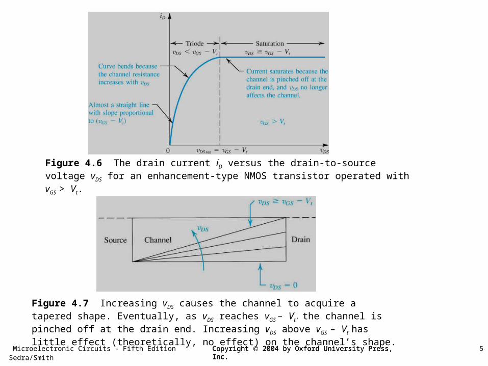
Microelectronic Circuits - Fifth Edition Sedra/Smith 2Copyright 2004 by Oxford University Press, Inc.Copyright 2004 by Oxford University Press, Inc.
Introduction - Transistors are three-terminal devices.- Voltage between two terminal controls the current flowing in the third terminal.
- Amplifiers, or switches.
Compared to Bipolar Junction Transistors (BJT), MOSTFETs;- Can be made quite small (require small area).- Can be manufactured with simple fabrication process.- Can be operated with little power.
- Digital and analog functions can be implemented almost exclusively ( i.e., with very few or no resistors).- Digital and analog functions can be implemented on the same IC chip (mixed-signal design).
- Can be integrated densely (>200 millions on a single IC chip, Very-large-scale-integrated circuit, VLSI).
4.1 Device Structure and Physical Operation
The enhancement-type MOSFET is the most widely used field-effect transistor.
4.1.1 Device Structure – (n-channel enhancement-type MOSFET = enhancement-type NMOS)
0.1~3 μm
0.2~100 μm2-~50 nm
MOS

Microelectronic Circuits - Fifth Edition Sedra/Smith 3Copyright 2004 by Oxford University Press, Inc.Copyright 2004 by Oxford University Press, Inc.
Figure 4.2 The enhancement-type NMOS transistor with a positive voltage applied to the gate. An n channel is induced at the top of the substrate beneath the gate.
Another name for the MOSFET: Insulated-gate FET, IGFET (almost no current through the gate : ~10 -15 A)
4.1.2 Operation with No gate VoltageBetween drain and source : Back-to-back pn junction
No current flow
4.1.3 Creating a Channel for current flow
- If a voltage is applied between drain and source, current flows through this n-channel. (NMOS)
- An n-channel is formed in a p-type substrate – inversion layer.
- Threshold voltage Vt : a voltage of υGS at which a sufficient number of mobile electrons accumulate in the channel region to form a conducting channel.(+0.5 ~ 1 V)
- The gate and the channel form a capacitor.
- The positive charges on the gate and the electrons in the channel develop an electric field.
- This electric field controls the current flow in the channel.
Field-Effect Transistor (FET) !

Microelectronic Circuits - Fifth Edition Sedra/Smith 4Copyright 2004 by Oxford University Press, Inc.Copyright 2004 by Oxford University Press, Inc.
The device acts as a resistance whose value is determined by υGS. Specifically, the channel conductance is proportional to υGS – Vt’ and thus iD is proportional to (υGS – Vt) υDS.
4.1.4 Applying a Small VDS (< 50 mV)
(υGS – Vt) : excess gate voltage, effective voltage, overdrive voltage
4.1.5 Operation as VDS increased.
- At υGD =υGS – υDS = Vt or υDS = υGS - Vt , the channel depth at the drain end is almost zero! – The channel is pinched off.
- Increasing υDS beyond this value has, theoretically, no effect on the channel shape and channel current.-Saturation!
V (4.1)DSsat GS t
- As υDS is increased υGD =υGS – υDS decreases and channel takes the tapered form, and resistance between the drain and gate increases.
When υDS = small or 0 V
Microelectronic Circuits - Fifth Edition Sedra/Smith 5Copyright 2004 by Oxford University Press, Inc.Copyright 2004 by Oxford University Press, Inc.
Figure 4.6 The drain current iD versus the drain-to-source voltage vDS for an enhancement-type NMOS transistor operated with vGS > Vt.
Figure 4.7 Increasing vDS causes the channel to acquire a tapered shape. Eventually, as vDS reaches vGS – Vt’ the channel is pinched off at the drain end. Increasing vDS above vGS – Vt has little effect (theoretically, no effect) on the channel’s shape.
Microelectronic Circuits - Fifth Edition Sedra/Smith 6Copyright 2004 by Oxford University Press, Inc.Copyright 2004 by Oxford University Press, Inc.
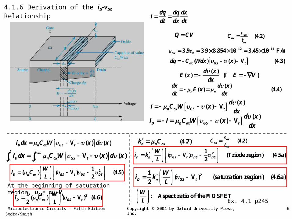
4.1.6 Derivation of the iD-vDS Relationship
(4.2)oxox
ox
Ct
12 1103.9 3.9 8.854 10 3.45 10 F/mox
( ) ( ) V (4.3)ox GS tdq C Wdx x ( )
( ) ( )d x
E x E Vdx
( )( ) (4.4)n n
dx d xE x
dt dx
dq dq dxi
dt dx dt
( )( ) Vn ox GS t
d xi C W x
dx
( )
( ) VD n ox GS t
d xi i C W x
dx
V ( ) ( )D n ox GS ti dx C W x d x
0 0V ( ) ( )
DSL
D n ox GS ti dx C W x d x
21( ) ( V ) (4.5)
2D n ox GS t DS DS
Wi C
L
21( ) ( V ) (4.6)
2D n ox GS t
Wi C
L
(4.7)n n oxk C
21( V ) (saturation region) (4.6a)
2D n GS t
Wi k
L
21( V ) (Triode region) (4.5a)
2D n GS t DS DS
Wi k
L
At the beginning of saturation region, υDS= υGS-Vt
: Aspect ratio of the MOSFETW
L Ex. 4.1 p245
(4.2)oxox
ox
Ct
Q CV
Microelectronic Circuits - Fifth Edition Sedra/Smith 7Copyright 2004 by Oxford University Press, Inc.Copyright 2004 by Oxford University Press, Inc.
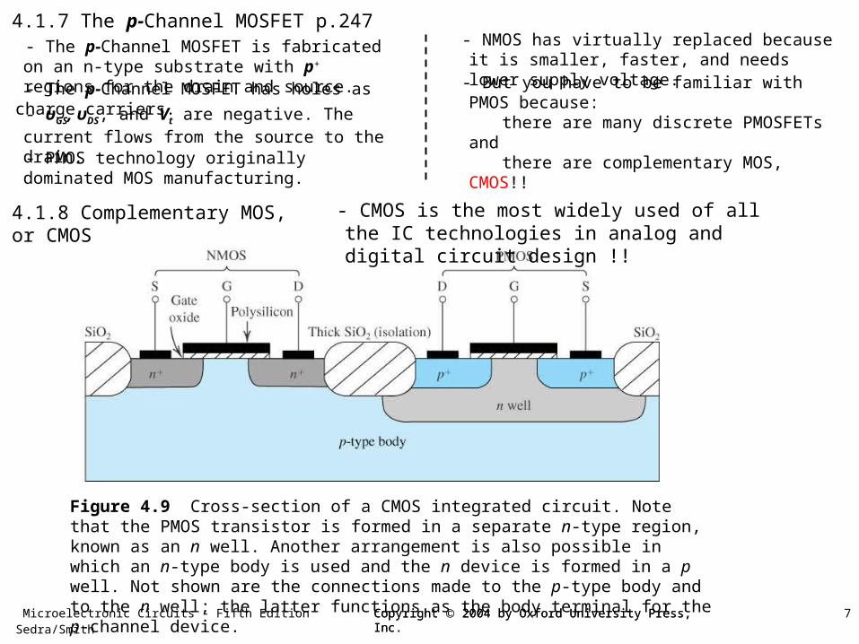
Figure 4.9 Cross-section of a CMOS integrated circuit. Note that the PMOS transistor is formed in a separate n-type region, known as an n well. Another arrangement is also possible in which an n-type body is used and the n device is formed in a p well. Not shown are the connections made to the p-type body and to the n well; the latter functions as the body terminal for the p-channel device.
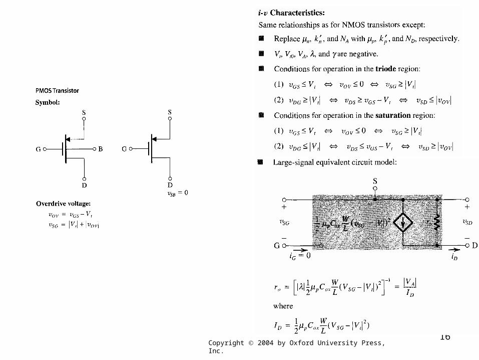
4.1.7 The p-Channel MOSFET p.247 - The p-Channel MOSFET is fabricated on an n-type substrate with p+ regions for the drain and source.
- The p-Channel MOSFET has holes as charge carriers.
- υGS, υDS, and Vt are negative. The current flows from the source to the drain.
- PMOS technology originally dominated MOS manufacturing.
- NMOS has virtually replaced because it is smaller, faster, and needs lower supply voltage.
- But you have to be familiar with PMOS because: there are many discrete PMOSFETs and there are complementary MOS, CMOS!!
4.1.8 Complementary MOS, or CMOS - CMOS is the most widely used of all the IC technologies in analog and digital circuit design !!
Microelectronic Circuits - Fifth Edition Sedra/Smith 8Copyright 2004 by Oxford University Press, Inc.Copyright 2004 by Oxford University Press, Inc.
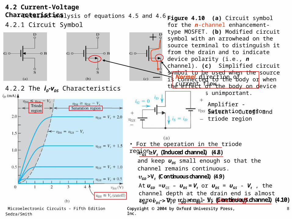
Figure 4.10 (a) Circuit symbol for the n-channel enhancement-type MOSFET. (b) Modified circuit symbol with an arrowhead on the source terminal to distinguish it from the drain and to indicate device polarity (i.e., n channel). (c) Simplified circuit symbol to be used when the source is connected to the body or when the effect of the body on device operation is unimportant.
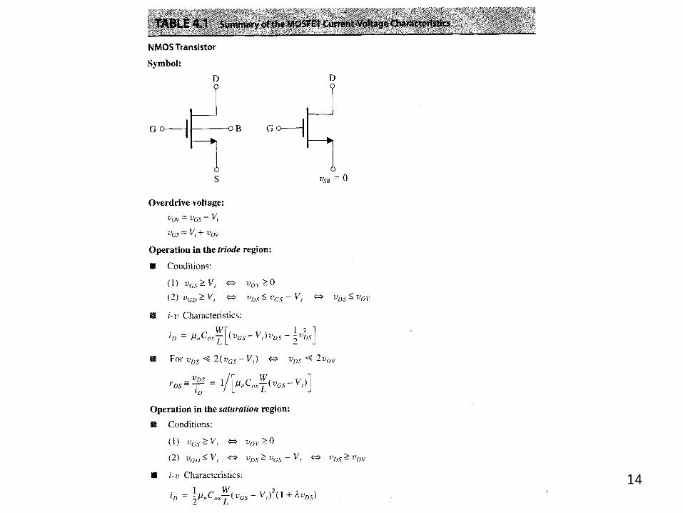
4.2 Current-Voltage Characteristics
4.2.1 Circuit Symbol
Detailed analysis of equations 4.5 and 4.6
Normal direction of current flow.
4.2.2 The iD-vDS Characteristics
Amplifier - Saturation region Switch – Cutoff and triode region
• For the operation in the triode region,
(Induced channel) (4.8)GS tV and keep υDS small enough so that the channel remains continuous.
>V (Continuous channel) (4.9)GD tAt υGD =υGS – υDS = Vt or υDS = υGS - Vt , the channel depth at the drain end is almost zero! – The channel is pinched off.
V ,GD DS t V (Continuous channel) (4.10)DS GS t
Microelectronic Circuits - Fifth Edition Sedra/Smith 9Copyright 2004 by Oxford University Press, Inc.Copyright 2004 by Oxford University Press, Inc.
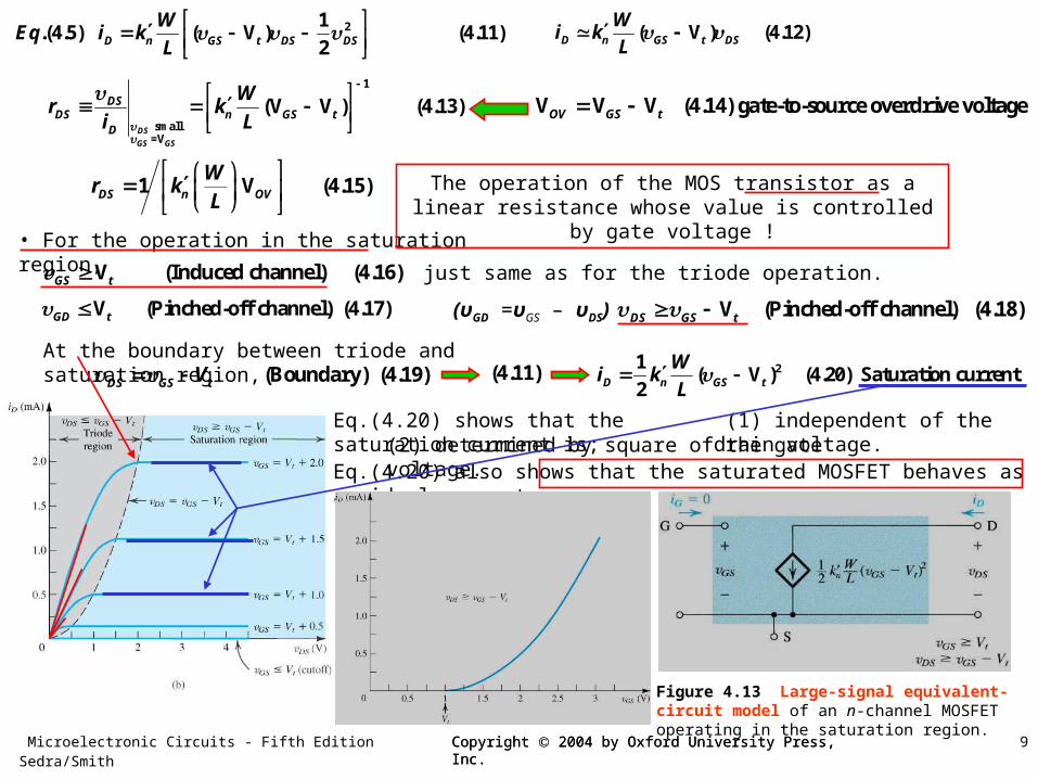
21.(4.5) ( V ) (4.11)
2D n GS t DS DS
WEq i k
L
( V ) (4.12)D n GS t DS
Wi k
L
1
small=V
(V V ) (4.13)DS
GS GS
DSDS n GS t
D
Wr k
i L
V V V (4.14) gate-to-source overdrive voltageOV GS t
1 V (4.15)DS n OV
Wr k
L
V (Induced channel) (4.16)GS t
• For the operation in the saturation region,
just same as for the triode operation.
V (Pinched-off channel) (4.17)GD t V (Pinched-off channel) (4.18)DS GS t (υGD =υGS – υDS)
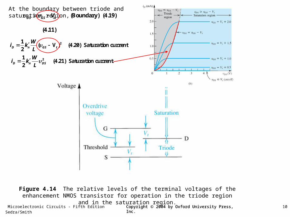
At the boundary between triode and saturation region, (Boundary) (4.19)DS GS tV 21
( V ) (4.20) Saturation current2D n GS t
Wi k
L (4.11)
Eq.(4.20) shows that the saturation current is; (1) independent of the drain voltage.(2) determined by square of the gate voltage.
Eq.(4.20) also shows that the saturated MOSFET behaves as an ideal current source.
Figure 4.13 Large-signal equivalent-circuit model of an n-channel MOSFET operating in the saturation region.
The operation of the MOS transistor as a linear resistance whose value is controlled by gate voltage !
Microelectronic Circuits - Fifth Edition Sedra/Smith 10Copyright 2004 by Oxford University Press, Inc.Copyright 2004 by Oxford University Press, Inc.
Figure 4.14 The relative levels of the terminal voltages of the enhancement NMOS transistor for operation in the triode region and in the saturation region.
At the boundary between triode and saturation region, (Boundary) (4.19)DS GS tV
21( V ) (4.20) Saturation current
2D n GS t
Wi k
L
(4.11)
21 (4.21) Saturation current
2D n DS
Wi k
L

Microelectronic Circuits - Fifth Edition Sedra/Smith 11Copyright 2004 by Oxford University Press, Inc.Copyright 2004 by Oxford University Press, Inc.
Figure 4.15 Increasing vDS beyond vDSsat causes the channel pinch-off point to move slightly away from the drain, thus reducing the effective channel length (by ΔL).
4.2.3 Finite Output Resistance in Saturation
21( V ) (4.20) Saturation current
2D n GS t
Wi k
L
Eq.(4.20) shows that the saturation current is independent of the drain voltage.
But, in practice, increasing υDS beyond υDSsat does affect the channel length.
The phenomenon that the channel length is reduced form L to L-ΔL is known as channel-length modulation. 2
2
2
1( V )
21 1
( V )2 1 ( )
1 1 ( V )
2
D n GS t
n GS t
n GS t
Wi k
L LW
kL L L
W Lk
L L
Assuming , DSL
( / 1)L L
211 ( )
2D n DS GS t
Wi k V
L L
21( V ) 1 (4.22)
2D n GS t DS
Wi k
L
-1let , process-technology parameter (V )L
With extrapolation, 1/ , Early voltageAV
: 5~50 [V/ m], entirely process-techology parameterA AV V L V
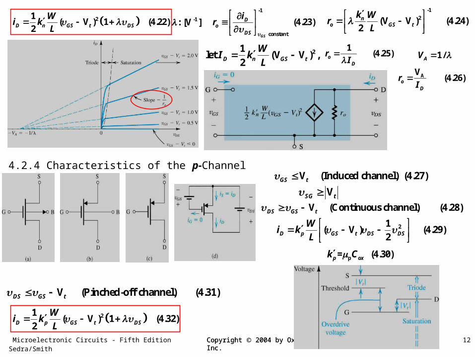
Microelectronic Circuits - Fifth Edition Sedra/Smith 12Copyright 2004 by Oxford University Press, Inc.Copyright 2004 by Oxford University Press, Inc.
-1
constant
(4.23)GS
Do
DS
ir
-1
2(V V ) (4.24)2
no GS t
k Wr
L
1 (4.25)o
D
rI
AV (4.26)o
D
rI
21let (V V ) ,
2D n GS t
WI k
L
21( V ) 1 (4.22)
2D n GS t DS
Wi k
L
4.2.4 Characteristics of the p-Channel MOSFETV (Induced channel) (4.27)GS t
VSG t
V (Pinched-off channel) (4.31)DS GS t
V (Continuous channel) (4.28)DS GS t
21( V ) (4.29)
2D p GS t DS DS
Wi k
L
p= (4.30)p oxk C
21( V ) 1 (4.32)
2D p GS t DS
Wi k
L
-1: [V ]
1/AV

Microelectronic Circuits - Fifth Edition Sedra/Smith 13Copyright 2004 by Oxford University Press, Inc.Copyright 2004 by Oxford University Press, Inc.
[ 2 2 ] (4.33)t t f SB fV V V
2 ( ) 0.6 V f physical parameter
4.2.5 The Role of the Substrate-The Body Effect- Usually, the source terminal is connected to the substrate (or body) terminal.
- In integrated circuit, many MOS transistors are fabricated on a single substrate.
- In order to maintain the cutoff condition for all the substrate-to-channel junctions, the substrate is usually connected to the most negative power supply in an NMOS circuit (the positive in a PMOS circuit).
- The reverse bias will widen the depletion region. - The channel depth is reduced.- To return the channel to its former states, υGS has to be increased.
A2( ) (4.34)s
ox
qNbody effect parameter
C
The body effect can cause considerable degradation in circuit performance (Chap. 6)
4.2.6 Temperature Effect
- The overall observed effect of a temperature increase is a decrease in drain current.
- This very interesting result is put to use in applying the MOSFET in power circuit (Chap. 11).
4.2.7 Breakdown and Input Protection
- Weak avalanche : υDS (20~150 V) breakdown between drain and substrate.
- Punch-through : υDS (~20 V) breakdown between drain and source for short-channel devices.
- υGS (>30 V) breakdown between gate and source.
14Copyright 2004 by Oxford University Press, Inc.

15Copyright 2004 by Oxford University Press, Inc.
16Copyright 2004 by Oxford University Press, Inc.
Microelectronic Circuits - Fifth Edition Sedra/Smith 17Copyright 2004 by Oxford University Press, Inc.Copyright 2004 by Oxford University Press, Inc.
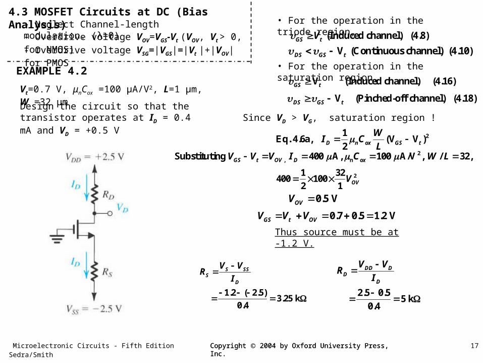
EXAMPLE 4.2
21Eq. 4.6a, (V V )
2D n ox GS t
WI C
L
21 32400 100
2 1 OVV
0.5 VOVV
0.7 0.5 1.2 VGS t OVV V V
1.2 ( 2.5) 3.25 k
0.4
S SSS
D
V VR
I
2.5 0.5 5 k
0.4
DD DD
D
V VR
I
4.3 MOSFET Circuits at DC (Bias Analysis) - Neglect Channel-length modulation. (λ=0)- Overdrive voltage VOV=VGS-Vt (VOV, Vt > 0, for NMOS)
- Overdrive voltage VSG=|VGS|=|Vt |+|VOV| for PMOS
Vt=0.7 V, μnCox =100 μA/V2, L=1 μm, W =32 μm
Design the circuit so that the transistor operates at ID = 0.4 mA and VD = +0.5 V
• For the operation in the triode region,
(Induced channel) (4.8)GS tV
V (Continuous channel) (4.10)DS GS t • For the operation in the saturation region,
V (Induced channel) (4.16)GS t
V (Pinched-off channel) (4.18)DS GS t
Since VD > VG, saturation region !
2, nSubstituting 400 A, 100 A/V , / 32,GS t OV D oxV V V I C W L
Thus source must be at -1.2 V.
Microelectronic Circuits - Fifth Edition Sedra/Smith 18Copyright 2004 by Oxford University Press, Inc.Copyright 2004 by Oxford University Press, Inc.
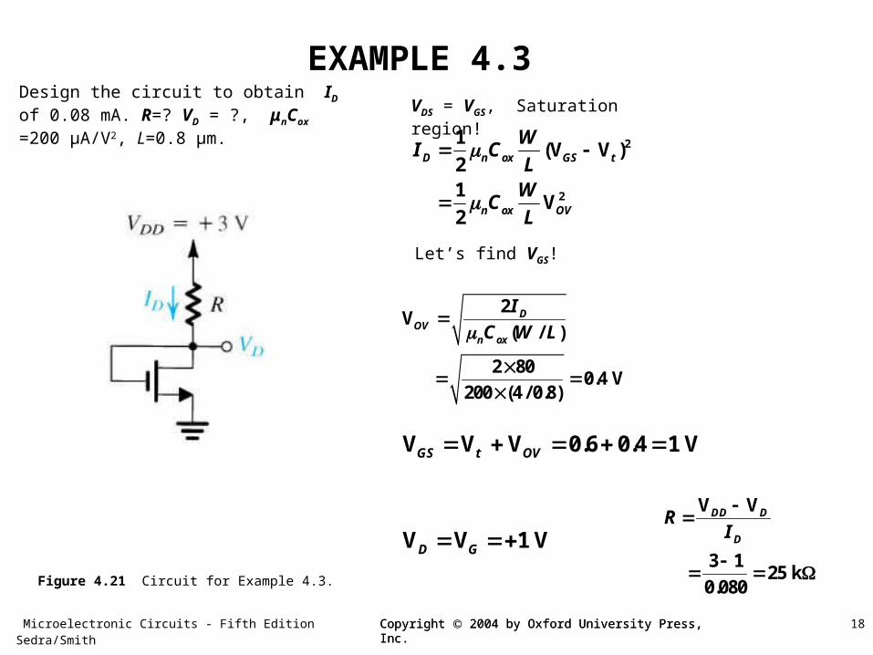
Figure 4.21 Circuit for Example 4.3.
EXAMPLE 4.3
2
2
1(V V )
21
V2
D n ox GS t
n ox OV
WI C
LW
CL
2V
( / )
2 80 0.4 V
200 (4 / 0.8)
DOV
n ox
I
C W L
V V V 0.6 0.4 1 VGS t OV
V V 1 VD G
V V
3 1 25 k
0.080
DD D
D
RI
Design the circuit to obtain ID of 0.08 mA. R=? VD = ?, μnCox =200 μA/V2, L=0.8 μm. VDS = VGS, Saturation region!
Let’s find VGS!

Microelectronic Circuits - Fifth Edition Sedra/Smith 19Copyright 2004 by Oxford University Press, Inc.Copyright 2004 by Oxford University Press, Inc.
EXAMPLE 4.4
21(V V ) 0.395 mA
2D n GS t DS DS
WI k
L
V V 5 0.112.4 k
0.395DD D
DD
RI
V 0.1253
0.395DS
DSD
rI
Vt=1 V, k’(W/L) 1 mA/V2
Design the circuit so that VD = +0.1 V.What is the effective resistance between drain and source?
Since VD < VG, and Vt =1 V, triode region !
In practice, 12 kΩ, 5%
EXAMPLE 4.5
2
2 1
10V V 10 5 V
10 10G
G DDG G
R
R R
V 5 6GS DI
2 21 1(V V) 1 (5 6 1)
2 2D n GS D
WI k I
L
218 25 8 0D DI I
0.5 mADI
V 0.5 6 3 VS
V 5 3 2 VGS
V 10 6 0.5 7 VD
?GV
?I ?DI
?DV
?SV
21 V, ( / ) 1 mA/V , 0t nV k W L
Assume saturation region operation.
Saturation region operation!
Microelectronic Circuits - Fifth Edition Sedra/Smith 20Copyright 2004 by Oxford University Press, Inc.Copyright 2004 by Oxford University Press, Inc.
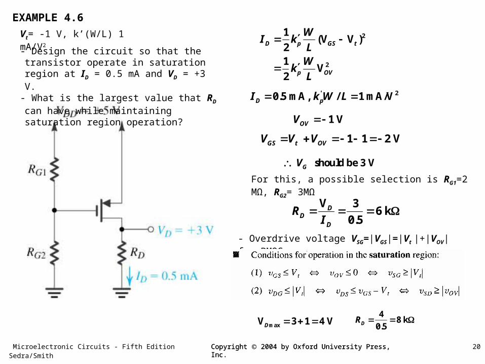
EXAMPLE 4.6
2
2
1(V V )
21
V2
D p GS t
p OV
WI k
LW
kL
1 VOVV
1 1 2 VGS t OVV V V
V 36 k
0.5D
DD
RI
maxV 3 1 4 VD 4
8 k0.5DR
Vt= -1 V, k’(W/L) 1 mA/V2
- Design the circuit so that the transistor operate in saturation region at ID = 0.5 mA and VD = +3 V.
- What is the largest value that RD can have while maintaining saturation region operation?
' 20.5 mA, / 1 mA/VD pI k W L
should be 3 VGV
For this, a possible selection is RG1=2 MΩ, RG2= 3MΩ
- Overdrive voltage VSG=|VGS|=|Vt |+|VOV| for PMOS
Microelectronic Circuits - Fifth Edition Sedra/Smith 21Copyright 2004 by Oxford University Press, Inc.Copyright 2004 by Oxford University Press, Inc.
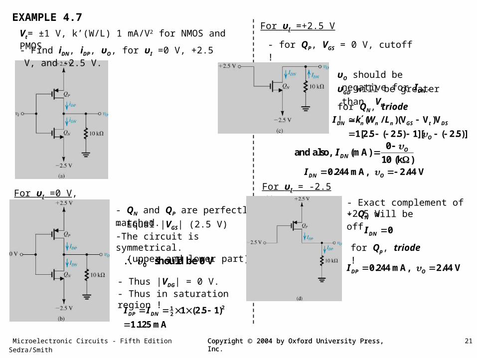
EXAMPLE 4.7
Vt= ±1 V, k’(W/L) 1 mA/V2 for NMOS and PMOS
- Find iDN, iDP, υO, for υI =0 V, +2.5 V, and -2.5 V.
- QN and QP are perfectly matched.
- Equal |VGS| (2.5 V)-The circuit is symmetrical. (upper and lower part)
O should be 0 V
- Thus |VDG| = 0 V.- Thus in saturation region !
212 1 (2.5 1)
1.125 mADP DNI I
For υI =+2.5 V
For υI =0 V,
- for QP, VGS = 0 V, cutoff !
υO should be negative for IDN.
( / )(V V )V
1[2.5 ( 2.5) 1][ ( 2.5)]DN n n n GS t DS
O
I k W L
υGD will be greater than Vt.
for QN, triode !
0and also, (mA)
10 (k )O
DNI
0.244 mA, 2.44 VDN OI
For υI = -2.5 V
- Exact complement of +2.5 V
for Qp, triode !
- QN will be off.
0DNI
0.244 mA, 2.44 VDP OI
Microelectronic Circuits - Fifth Edition Sedra/Smith 22Copyright 2004 by Oxford University Press, Inc.Copyright 2004 by Oxford University Press, Inc.
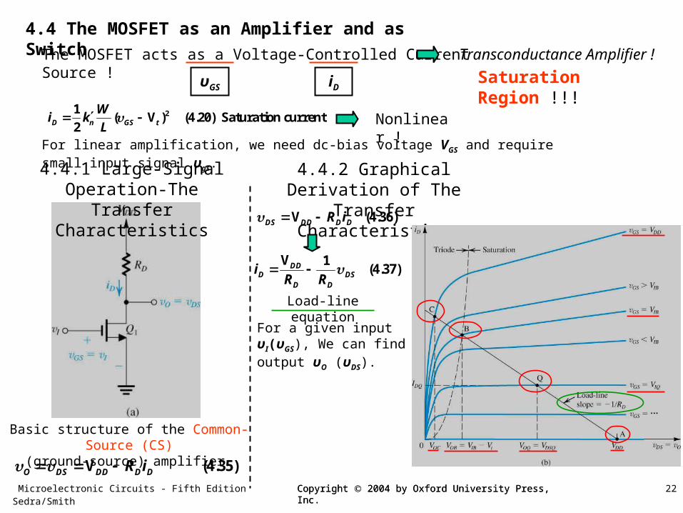
Basic structure of the Common-Source (CS) (ground-source) amplifier.
4.4 The MOSFET as an Amplifier and as Switch
The MOSFET acts as a Voltage-Controlled Current Source !
υGS iD
Transconductance Amplifier !
21( V ) (4.20) Saturation current
2D n GS t
Wi k
L Nonlinear !
For linear amplification, we need dc-bias voltage VGS and require small input signal υgs.
4.4.1 Large-Signal Operation-The Transfer Characteristics
V (4.35)O DS DD D DR i
4.4.2 Graphical Derivation of The Transfer Characteristics
V (4.36)DS DD D DR i
V 1 (4.37)DD
D DSD D
iR R
Load-line equation
For a given input υI(υGS), We can find output υO (υDS).
Saturation Region !!!
Microelectronic Circuits - Fifth Edition Sedra/Smith 23Copyright 2004 by Oxford University Press, Inc.Copyright 2004 by Oxford University Press, Inc.
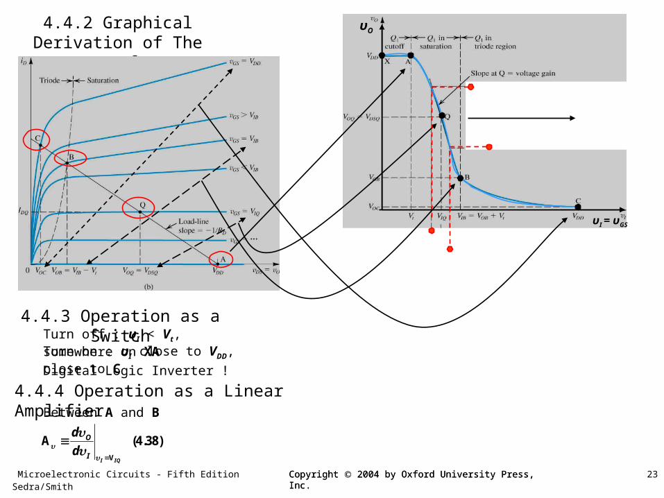
4.4.2 Graphical Derivation of The Transfer Characteristics
υI = υGS
υO
4.4.3 Operation as a SwitchTurn off : υI < Vt, somewhere on XATurn on : υI close to VDD, close to C
Digital Logic Inverter !
4.4.4 Operation as a Linear AmplifierBetween A and B
V
A (4.38)I IQ
O
I
d
d
Microelectronic Circuits - Fifth Edition Sedra/Smith 24Copyright 2004 by Oxford University Press, Inc.Copyright 2004 by Oxford University Press, Inc.
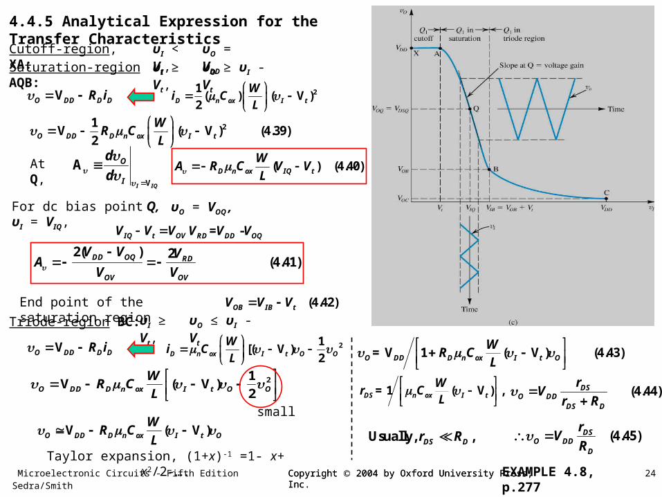
4.4.5 Analytical Expression for the Transfer Characteristics
Cutoff-region, XA: υI < Vt, υO = VDD
Saturation-region AQB: υI ≥ Vt, υO ≥ υI - Vt
21( ) ( V )
2D n ox I t
Wi C
L
VO DD D DR i
21V ( V ) (4.39)
2O DD D n ox I t
WR C
L
At Q,V
AI IQ
O
I
d
d
( ) (4.40)D n ox IQ t
WA R C V V
L
2( ) 2 (4.41)DD OQ RD
OV OV
V V VA
V V
(4.42)OB IB tV V V
For dc bias point Q, υI = VIQ, υO = VOQ ,
IQ t OVV V V = - RD DD OQV V V
End point of the saturation region
Triode-region BC: υI ≥ Vt, υO ≤ υI - Vt
VO DD D DR i 21[( V )
2D n ox I t O O
Wi C
L
21
V ( V )2O DD D n ox I t O O
WR C
L
V ( V )O DD D n ox I t O
WR C
L
small
= V 1 ( V ) (4.43)O DD D n ox I t O
WR C
L
= 1 ( V ) ,DS n ox I t
Wr C
L
(4.44)DSO DD
DS D
rV
r R
(4.45)DSO DD
D
rV
R Usually, ,DS Dr R
Taylor expansion, (1+x)-1 =1- x+ x2/2-….EXAMPLE 4.8, p.277
Microelectronic Circuits - Fifth Edition Sedra/Smith 25Copyright 2004 by Oxford University Press, Inc.Copyright 2004 by Oxford University Press, Inc.
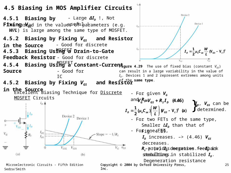
Figure 4.29 The use of fixed bias (constant VGS) can result in a large variability in the value of ID. Devices 1 and 2 represent extremes among units of the same type.
21(V V )
2D n ox GS t
WI C
L
4.5 Biasing in MOS Amplifier Circuits
4.5.1 Biasing by Fixing VGS
4.5.2 Biasing by Fixing VGS and Resistor in the Source
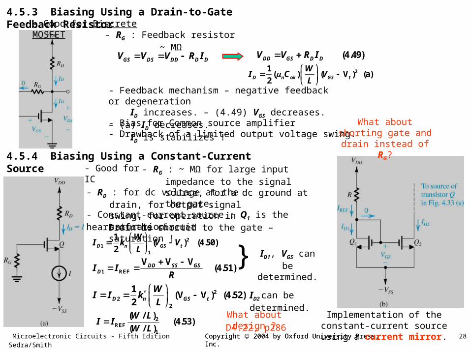
4.5.3 Biasing Using a Drain-to-Gate Feedback Resistor
4.5.4 Biasing Using a Constant-Current Source
- Large ΔID !, Not useful !
4.5.2 Biasing by Fixing VGS and Resistor in the Source
- Good for IC
Excellent Biasing Technique for Discrete MOSFET Circuits
- Good for discrete MOSFET
- Good for discrete MOSFET
(4.46)G GS S DV V R I
Smaller ΔID than that of Fig. 4.39
Rs provides negative feedback resulting in stabilized ID. Degeneration resistance
- For given VG and RS,
21( ) ( V ) (a)
2D n ox GS t
WI C V
L
} ID, VGS can be
determined.
- For one FET,
- For two FETs of the same type,
ID increases. –> (4.46) VGS decreases. –> (a) ID decreases.–> ID is stabilizes.
The spread in the values of parameters (e.g. W/L) is large among the same type of MOSFET.
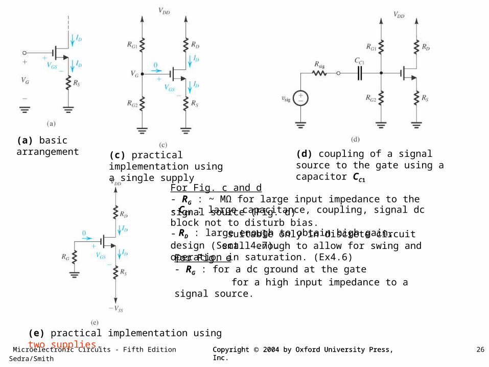
Microelectronic Circuits - Fifth Edition Sedra/Smith 26Copyright 2004 by Oxford University Press, Inc.Copyright 2004 by Oxford University Press, Inc.
(e) practical implementation using two supplies.
(a) basic arrangement
(c) practical implementation using a single supply
(d) coupling of a signal source to the gate using a capacitor CC1
For Fig. c and d- RG : ~ MΩ for large input impedance to the signal source (Fig. d)- CC1 : large capacitance, coupling, signal dc block not to disturb bias. suitable only in discrete circuit design (Sect. 4.7).- RD : large enough to obtain high gain, small enough to allow for swing and operation in saturation. (Ex4.6)For Fig. e- RG : for a dc ground at the gate for a high input impedance to a signal source.

Microelectronic Circuits - Fifth Edition Sedra/Smith 27Copyright 2004 by Oxford University Press, Inc.Copyright 2004 by Oxford University Press, Inc.
Figure 4.31 Circuit for Example 4.9.
EXAMPLE 4.9Design! Vt=1 V, k’(W/L) 1 mA/V2
Sol) As a rule of thumb for design,
One-third of the power supply voltage as a drop across each of RD, MOSFET, RS.
V V 15 1010 k
0.5DD D
DD
RI
V 510 k
0.5S
SS
RR
212 ( / )VD n OVI k W L
2120.5 1 VOV
V V V 1 1 2 VGS t OV
V V V 5 2 7 VG S GS
Microelectronic Circuits - Fifth Edition Sedra/Smith 28Copyright 2004 by Oxford University Press, Inc.Copyright 2004 by Oxford University Press, Inc.
GS DS DD D DV V V R I (4.49)DD GS D DV V R I
4.5.3 Biasing Using a Drain-to-Gate Feedback Resistor- Good for Discrete MOSFET
- RG : Feedback resistor ~ MΩ
- Feedback mechanism – negative feedback or degeneration ID increases. – (4.49) VGS decreases. – (a) ID decreases. ID is stabilizes !- Bias for Common source amplifier- Drawback of a limited output voltage swing.
4.5.4 Biasing Using a Constant-Current Source- Good for IC - RG : ~ MΩ for large input impedance to the
signal source, for a dc ground at the gate.- RD : for dc voltage at the drain, for output
signal swing, for operation in saturation.- Constant-current source : Q1 is the heart of the circuit
Drain is shorted to the gate – saturation !2
11
1( ) (4.50)
2D n GS t
WI k V V
L
1 REF
V V V (4.51) DD SS GS
DI IR
22
2
1(V V ) (4.52)
2D n GS t
WI I k
L
2REF
1
( / ) (4.53)
( / )
W LI I
W L
Implementation of the constant-current source using a current mirror.
} ID1, VGS can be determined.
ID2 can be determined.
What about design ?
D4.22, p286
21( ) ( V ) (a)
2D n ox GS t
WI C V
L
What about shorting gate and drain instead of RG?

Microelectronic Circuits - Fifth Edition Sedra/Smith 29Copyright 2004 by Oxford University Press, Inc.Copyright 2004 by Oxford University Press, Inc.
Figure 4.34 Conceptual circuit utilized to study the operation of the MOSFET as a small-signal amplifier.
21For dc bias current, (V V ) (4.54)
2D n GS t
WI k
L
(4.55)DS D DD D DV V V R I For saturation, we must have D GS tV V V
4.6 Small-Signal Operation and Models
4.6.2 The signal current in the drain terminal
V (4.56)GS GS gs 2
2 2
1(V V )
21 1
(V V ) (V V ) + (4.47)2 2
D n GS gs t
n GS t n GS t gs n gs
Wi k
LW W W
k k kL L L
dc bias current Current proportional to input Nonlinear distortion
To reduce the nonlinear distortion,
21(V V )
2 n gs n GS t gs
W Wk k
L L 2(V V ) (4.58)gs GS t
or 2V (4.59)gs OV If this small-signal condition is satisfied,
(4.60)D D di I i where (V V )d n GS t gs
Wi k
L
(V V ) (4.61) transconductancedm n GS t
gs
i Wg k
L
(V ) (4.62)m n OV
Wg k
L
V
(4.63)GS GS
Dm
GS
ig
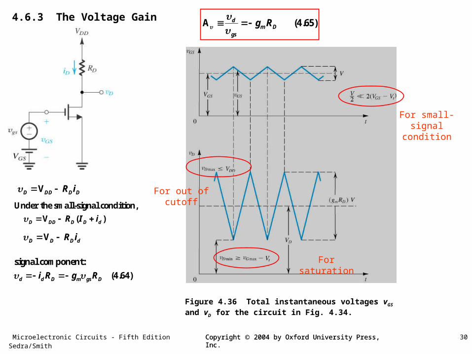
Microelectronic Circuits - Fifth Edition Sedra/Smith 30Copyright 2004 by Oxford University Press, Inc.Copyright 2004 by Oxford University Press, Inc.
VD DD D DR i
Under the small-signal condition,
V ( )D DD D D dR I i
VD D D dR i
signal component:
(4.64)d d D m gs Di R g R
A (4.65)dm D
gs
g R 4.6.3 The Voltage Gain
Figure 4.36 Total instantaneous voltages vGS and vD for the circuit in Fig. 4.34.
For small-signal condition
For saturation
For out of cutoff

Microelectronic Circuits - Fifth Edition Sedra/Smith 31Copyright 2004 by Oxford University Press, Inc.Copyright 2004 by Oxford University Press, Inc.
21V (4.67)
2D n OV
WI k
L
AA
V (4.66) (Eq. 4.26 in Sect. 4.2.3), V 1/o
D
rI
A ( // ) (4.68)dm D o
gs
g R r
4.6.4 Separating the DC Analysis and the Signal Analysis
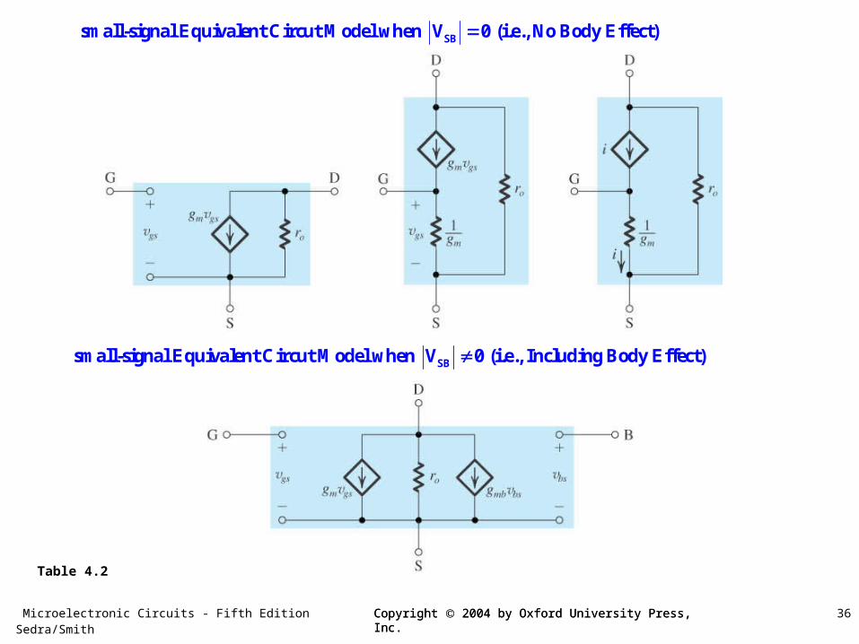
4.6.5 Small-signal Equivalent-Circuit ModelFET behaves as a voltage-controlled current source.
The input impedance is very, very high.
The output impedance is also high.
(b) including the effect of channel-length modulation, modeled by output resistance ro = |VA| /ID.
(a) neglecting the dependence of iD
on vDS in saturation (the channel-length modulation effect
Small-signal models for the MOSFET
For the signal analysis,Ideal constant voltage sources are replaced by short circuits. Ideal constant current sources are replaced by open circuits.
To include the channel-length modulation,
For PMOS,'use , , , , GS t OV A pV V V V k
Microelectronic Circuits - Fifth Edition Sedra/Smith 32Copyright 2004 by Oxford University Press, Inc.Copyright 2004 by Oxford University Press, Inc.
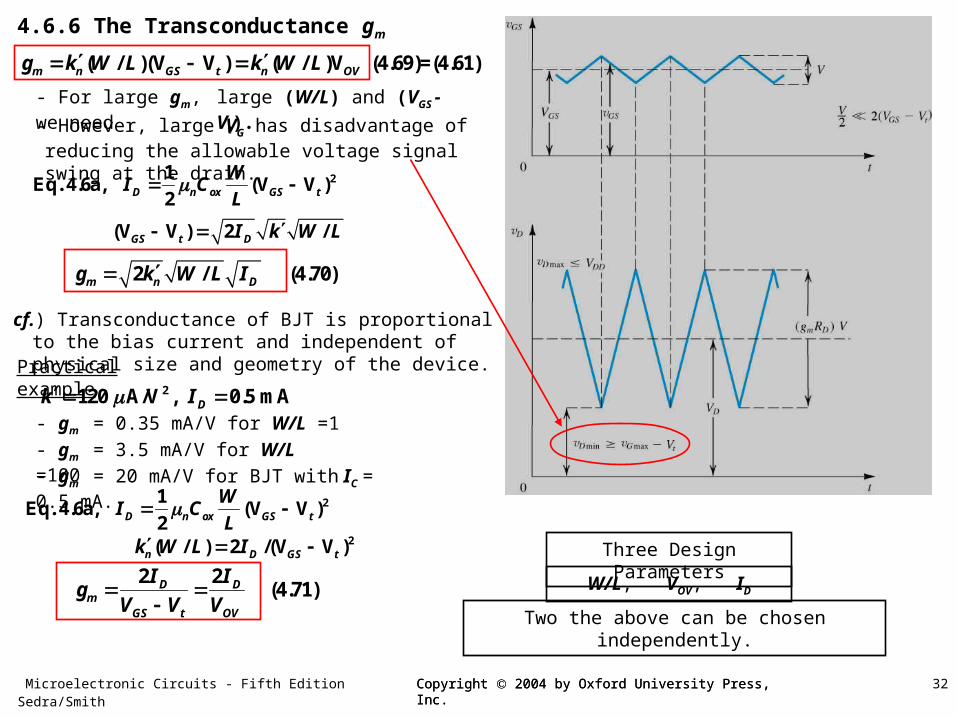
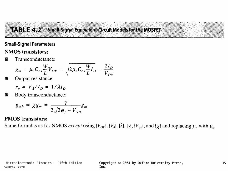
( / )(V V ) ( / )V (4.69)=(4.61)m n GS t n OVg k W L k W L
2 / (4.70)m n Dg k W L I
2 2 (4.71)D D
mGS t OV
I Ig
V V V
4.6.6 The Transconductance gm
- For large gm, we need large (W/L) and (VGS - Vt).
- However, large VG has disadvantage of reducing the allowable voltage signal swing at the drain.
21Eq. 4.6a, (V V )
2D n ox GS t
WI C
L
(V V ) 2 /GS t DI k W L
cf.) Transconductance of BJT is proportional to the bias current and independent of physical size and geometry of the device.
Practical example2120 A/V , 0.5 mADk I
- gm = 0.35 mA/V for W/L =1
- gm = 3.5 mA/V for W/L =100
- gm = 20 mA/V for BJT with IC = 0.5 mA.21
Eq. 4.6a, (V V )2D n ox GS t
WI C
L
2( / ) 2 /(V V )n D GS tk W L I Three Design Parameters
W/L, VOV, ID
Two the above can be chosen independently.

Microelectronic Circuits - Fifth Edition Sedra/Smith 33Copyright 2004 by Oxford University Press, Inc.Copyright 2004 by Oxford University Press, Inc.
EXAMPLE 4.10Vt=1.5 V, kn’ (W/L) =0.25 mA/V2, VA = 50 V.
Small-signal gain=?, input resistance=?, maximum input signal =?
( / )( )m n GS tg k W L V V Sol) ?GS DV V
21Eq. 4.6a, ( )
2D n GS t
WI k V V
L
15 15 10 (4.74)D D D DV R I I }AV
(4.66) oD
rI
in ?i
i
Ri
( // // )o m gs D L og R R r A ( // // )
0.725(10 // 10 // 47) 3.3 V/V
om D L o
i
g R R r
( ) / 1
4.3 [1 ( 3.3)]
i oi i o G
G i
i i
G G
i RR
R R
in 2.33 M4.3
i G
i
RR
i
To stay in saturation region,
VDS GS t min max VDS GS t
i iDS GS tV A V V
4.4 3.3 4.4 1.5i i
0.34 Vi
Microelectronic Circuits - Fifth Edition Sedra/Smith 34Copyright 2004 by Oxford University Press, Inc.Copyright 2004 by Oxford University Press, Inc.
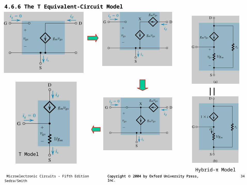
4.6.6 The T Equivalent-Circuit Model
T Model
Hybrid-π Model
Microelectronic Circuits - Fifth Edition Sedra/Smith 35Copyright 2004 by Oxford University Press, Inc.Copyright 2004 by Oxford University Press, Inc.
Microelectronic Circuits - Fifth Edition Sedra/Smith 36Copyright 2004 by Oxford University Press, Inc.Copyright 2004 by Oxford University Press, Inc.
Table 4.2
SBsmall-signal Equivalent Circut Model when V 0 (i.e., No Body Effect)
SBsmall-signal Equivalent Circut Model when V 0 (i.e., Including Body Effect)

Microelectronic Circuits - Fifth Edition Sedra/Smith 37Copyright 2004 by Oxford University Press, Inc.Copyright 2004 by Oxford University Press, Inc.
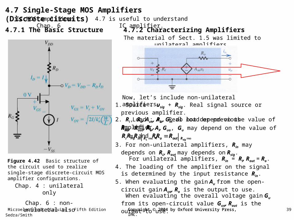
4.7 Single-Stage MOS Amplifiers (Discrete circuits)
Microelectronic Circuits - Fifth Edition Sedra/Smith 38Copyright 2004 by Oxford University Press, Inc.Copyright 2004 by Oxford University Press, Inc.
Microelectronic Circuits - Fifth Edition Sedra/Smith 39Copyright 2004 by Oxford University Press, Inc.Copyright 2004 by Oxford University Press, Inc.
Figure 4.42 Basic structure of the circuit used to realize single-stage discrete-circuit MOS amplifier configurations.
4.7 Single-Stage MOS Amplifiers (Discrete circuits)IC MOS amplifiers : Chap. 6
4.7.1 The Basic Structure
4.7 is useful to understand IC amplifier.
4.7.2 Characterizing AmplifiersThe material of Sect. 1.5 was limited to unilateral
amplifiers.
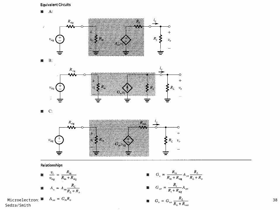
Now, let’s include non-unilateral amplifiers.1. Source : υsig + Rsig. Real signal source or previous amplifier. Load : RL. Real load or previous amplifier.2. Ri, Ro, Aυo, Ais, Gm do not depend on the value of Rsig and RL.
Rin, Rout, Aυ, Ai, Gυo, Gυ may depend on the value of Rsig and RL.
, L sigi in R o out RR R R R
3. For non-unilateral amplifiers, Rin may depends on RL, Rout may depends on Rsig.
For unilateral amplifiers, Rin = Ri, Rout = Ro.
4. The loading of the amplifier on the signal is determined by the input resistance Rin.
5. When evaluating the gain Aυ from the open-circuit gain Aυo, Ro is the output to use.
When evaluating the overall voltage gain Gυ from its open-circuit value Gυo, Rout is the output to use.
Chap. 4 : unilateral only
Chap. 6 : non-unilateral also
Microelectronic Circuits - Fifth Edition Sedra/Smith 40Copyright 2004 by Oxford University Press, Inc.Copyright 2004 by Oxford University Press, Inc.
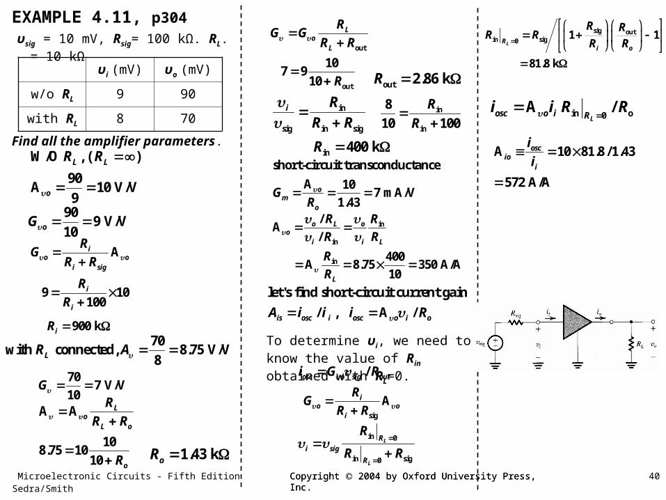
EXAMPLE 4.11, p304
W/O , ( )
90A 10 V/V
9
L L
o
R R
909 V/V
10oG
A
9 10100
io o
i sig
i
i
RG
R R
R
R
900 kiR 70
with connected, 8.75 V/V8LR A
707 V/V
10G
υsig = 10 mV, Rsig= 100 kΩ. RL. = 10 kΩ
υi (mV) υo (mV)
w/o RL 9 90
with RL 8 70
Find all the amplifier parameters.
A A
108.75 10
10
Lo
L o
o
R
R R
R
1.43 koR
out
out
10 7 9
10
Lo
L
RG G
R R
R
out 2.86 kR
in
sig in sig
i R
R R
in
in
8
10 100
R
R
in 400 kR short-circuit transconductance
A 107 mA/V
1.43o
mo
GR
in
in
in
/A
/
400 A 8.75 350 A/A
10
o L oo
i i L
L
R R
R R
R
R
let's find short-circuit current gain
/ , A /is osc i osc o i oA i i i R
/osc o sig outi G R
sig
Aio o
i
RG
R R
in 0
in sig0
L
L
R
i sig
R
R
R R
To determine υi, we need to know the value of Rin obtained with RL=0.
sig outin sig0
1 1
81.8 k
LRi o
R RR R
R R
in o0A /
Losc o i R
i i R R
A 10 81.8 / 1.43
572 A/A
oscio
i
i
i

Microelectronic Circuits - Fifth Edition Sedra/Smith 41Copyright 2004 by Oxford University Press, Inc.Copyright 2004 by Oxford University Press, Inc.
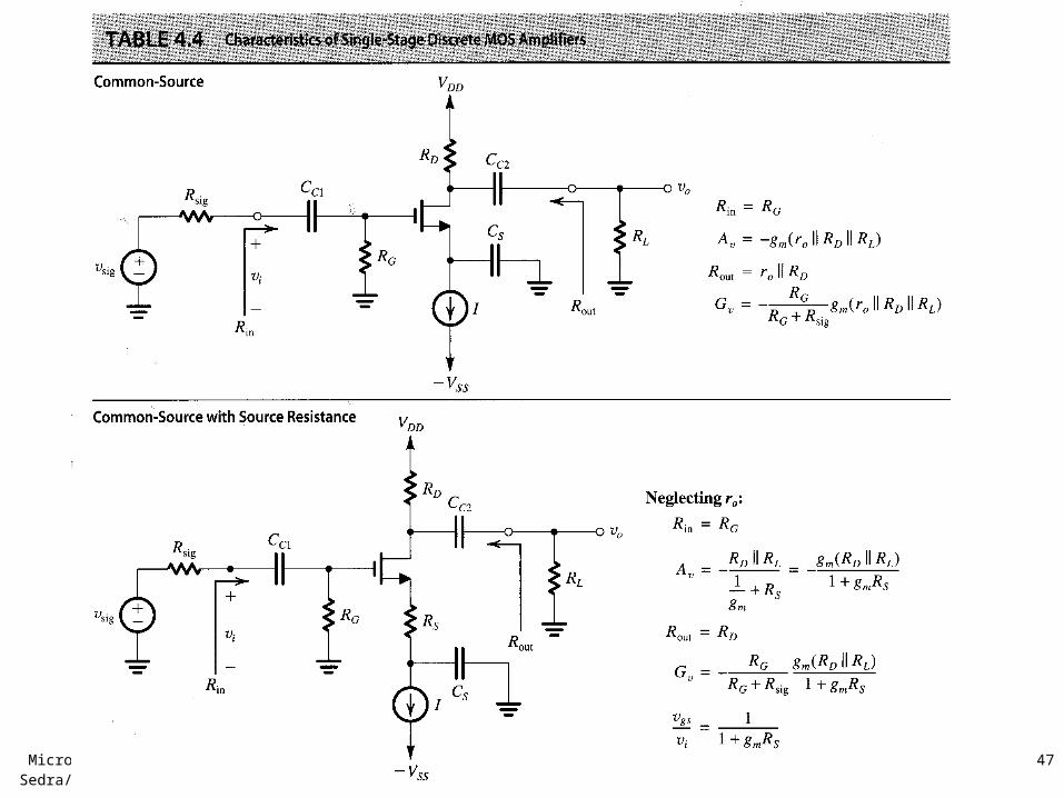
Figure 4.43 (a) Common-source amplifier based on the circuit of Fig. 4.42.
4.7.3 The Common-Source (CS) Amplifiers- The most widely used of all MOSFET amplifier circuits.
Bypass capacitor (~μF)For signal ground
Bypass capacitor (~μF)
(b) Equivalent circuit of the amplifier for small-signal analysis.
(c) Small-signal analysis performed directly on the amplifier circuit with the MOSFET model implicitly utilized.
0gi in G (4.78)iR R R
Ginsig sig
in sig G sig
(4.79)i
RR
R R R R
G (~M ) sigR R sigi
igs
gs ( )o m o D Lg r R R }A ( ) (4.80)m o D Lg r R R
A ( ) (4.81)o m o Dg r R
in
in sig
G
G sig
A
( ) (4.82)m o D L
RG
R R
Rg r R R
R R
out (4.83)o DR r R
( / )(V V ) ( / )V (4.69)=(4.61)m n GS t n OVg k W L k W L 2 / (4.70)m n Dg k W L I2 2
(4.71)D Dm
GS t OV
I Ig
V V V

Microelectronic Circuits - Fifth Edition Sedra/Smith 42Copyright 2004 by Oxford University Press, Inc.Copyright 2004 by Oxford University Press, Inc.
Figure 4.44 (a) Common-source amplifier with a resistance RS in the source lead.
4.7.4 The Common-Source (CS) Amplifier with a Source Resistance
(b) Small-signal T-equivalent circuit with ro neglected.
- The effect ro is not important (SPICE) in discrete-circuit amp.
- The effect ro plays major role and must be taken into account in IC amp.
in (4.84)i GR R R G
sigG sig
(4.85)i
R
R R
1/1 (4.86)
1/ 1m i
gs im m S m S
gi
g g R g R
(4.87)1 / 1
i m id
m S m S
gi i
g R g R
( )( )
1m D L
o d D L im S
g R Ri R R
g R
( )A (4.88)
1o m D L
i m S
g R R
g R
A (4.89)1
m Do
m S
g R
g R
o
sig
G
- Rs increases dc bias stability. (Sect. 4.5)
- Rs decreases gain. (4.90)
Need trade-off !
sig
( ) (4.90)
1G m D L
G m S
R g R R
R R g R
- Rs increases the bandwidth (Sect. 4.12).
- Rs decreases υgs to reduce nonlinear distortion. (4.86), (4.58) }
Split RS !!
RSac
RSdc

Microelectronic Circuits - Fifth Edition Sedra/Smith 43Copyright 2004 by Oxford University Press, Inc.Copyright 2004 by Oxford University Press, Inc.
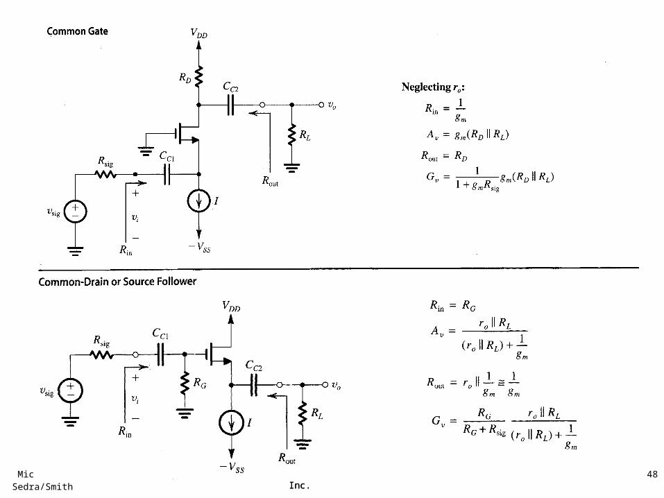
Figure 4.45 (a) A common-gate amplifier based on the circuit of Fig. 4.42.
4.7.5 The Common-Gate (CG) Amplifier
(b) A small-signal equivalent circuit of the amplifier in (a).
(c) The common-gate amplifier fed with a current-signal input.
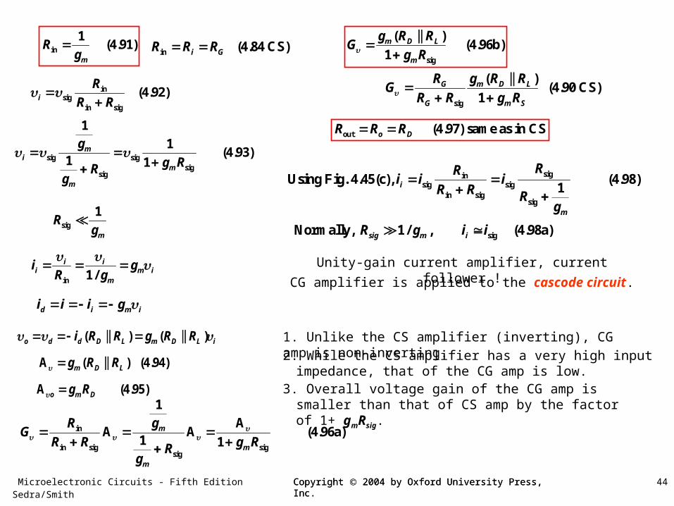
Microelectronic Circuits - Fifth Edition Sedra/Smith 44Copyright 2004 by Oxford University Press, Inc.Copyright 2004 by Oxford University Press, Inc.
in
1 (4.91)
m
Rg
insig
in sig
(4.92)i
R
R R
sig sigsig
sig
1
1 (4.93)
1 1m
im
m
g
g RRg
sig
1
m
Rg
in 1/i i
i m im
i gR g
d i m ii i i g
( ) ( )o d d D L m D L ii R R g R R
A ( ) (4.94)m D Lg R R
A (4.95)o m Dg R
in
in sig sigsig
1A
A A (4.96a)1 1
m
m
m
gRG
R R g RRg
sig
( ) (4.96b)
1m D L
m
g R RG
g R
out (4.97) same as in CSo DR R R
siginsig sig
in sigsig
Using Fig. 4.45(c), (4.98)1i
m
RRi i i
R R Rg
sig (4.98a)ii i
in (4.84 CS)i GR R R
sig
( ) (4.90 CS)
1G m D L
G m S
R g R RG
R R g R
1. Unlike the CS amplifier (inverting), CG amp is non-inverting.
2. While the CS amplifier has a very high input impedance, that of the CG amp is low.
3. Overall voltage gain of the CG amp is smaller than that of CS amp by the factor of 1+ gmRsig.
Normally, 1 / ,sig mR g
Unity-gain current amplifier, current follower !
CG amplifier is applied to the cascode circuit.
Microelectronic Circuits - Fifth Edition Sedra/Smith 45Copyright 2004 by Oxford University Press, Inc.Copyright 2004 by Oxford University Press, Inc.
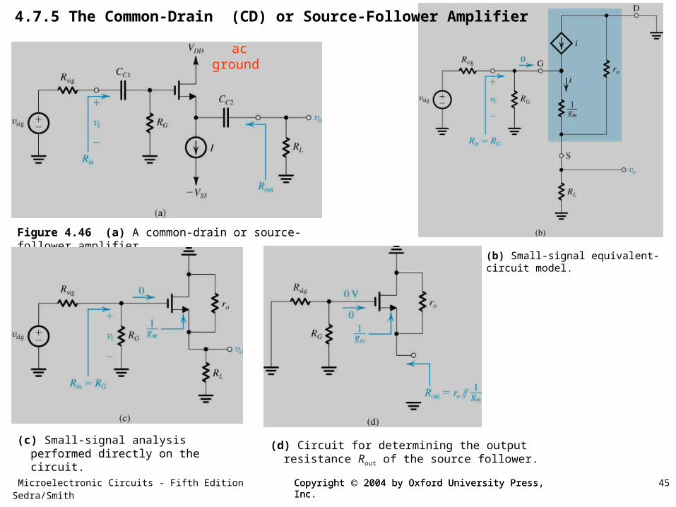
Figure 4.46 (a) A common-drain or source-follower amplifier.
4.7.5 The Common-Drain (CD) or Source-Follower Amplifier
ac ground
(b) Small-signal equivalent-circuit model.
(c) Small-signal analysis performed directly on the circuit.
(d) Circuit for determining the output resistance Rout of the source follower.

Microelectronic Circuits - Fifth Edition Sedra/Smith 46Copyright 2004 by Oxford University Press, Inc.Copyright 2004 by Oxford University Press, Inc.
Ginsig sig
in sig G sig
= (4.100)i
RR
R R R R
in (4.99)GR R
sigi
(4.101)1
( )
L oi
L om
R r
R rg
A (4.102)1
( )
L o
L om
R r
R rg
A (4.103)1
oo
om
r
rg
Usually, ,G sigR R
Normally, 1 / ,o mr g
A 1 o means the voltage at the source follows that at the gate.
Source follower !
In many discrete-circuit application, ,o Lr R
A (4.102a)1
Lo
Lm
R
Rg
sig
(4.104)1
( )
G L o
GL o
m
R R rG
R R R rg
out
1 (4.105)o
m
R rg
out
1 (4.106)
m
Rg
For , 1 / , ,G sig o m o LR R r g r R 1G
Normally, 1 / ,o mr g
The source follower has a very high input impedance, a relatively low output impedance, a gain less than but close to unity.
Unity-gain buffer amplifier ! (Sect. 1.5)
Output stage of multi-stage amplifier !
Microelectronic Circuits - Fifth Edition Sedra/Smith 47Copyright 2004 by Oxford University Press, Inc.Copyright 2004 by Oxford University Press, Inc.
Microelectronic Circuits - Fifth Edition Sedra/Smith 48Copyright 2004 by Oxford University Press, Inc.Copyright 2004 by Oxford University Press, Inc.

Microelectronic Circuits - Fifth Edition Sedra/Smith 49Copyright 2004 by Oxford University Press, Inc.Copyright 2004 by Oxford University Press, Inc.
Microelectronic Circuits - Fifth Edition Sedra/Smith 50Copyright 2004 by Oxford University Press, Inc.Copyright 2004 by Oxford University Press, Inc.
Microelectronic Circuits - Fifth Edition Sedra/Smith 51Copyright 2004 by Oxford University Press, Inc.Copyright 2004 by Oxford University Press, Inc.