The Potential of Photovoltaics (Presentation) - NREL · The Potential of Photovoltaics NREL is a...
38
AIMCAL 2008 2008 Fall Conference Vacuum Web Coating Brent P. Nelson October 22, 2008 The Potential of Photovoltaics NREL is a national laboratory of the U.S. Department of Energy Office of Energy Efficiency and Renewable Energy operated by the Alliance for Sustainable Energy, LLC NREL/PR-520-44106 Presented at the Association of Industrial Metallizers, Coaters and Laminators (AIMCAL) Fall Technical Conference 2008 and 22nd International Vacuum Web Coating Conference held October 19-22, 2008 in Myrtle Beach, South Carolina.
Transcript of The Potential of Photovoltaics (Presentation) - NREL · The Potential of Photovoltaics NREL is a...
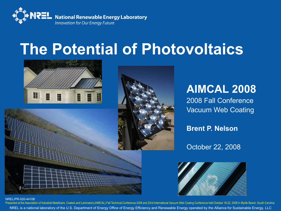
AIMCAL 20082008 Fall ConferenceVacuum Web Coating
Brent P. Nelson
October 22, 2008
The Potential of Photovoltaics
NREL is a national laboratory of the U.S. Department of Energy Office of Energy Efficiency and Renewable Energy operated by the Alliance for Sustainable Energy, LLC
NREL/PR-520-44106Presented at the Association of Industrial Metallizers, Coaters and Laminators (AIMCAL) Fall Technical Conference 2008 and 22nd International Vacuum Web Coating Conference held October 19-22, 2008 in Myrtle Beach, South Carolina.
National Renewable Energy Laboratory Innovation for Our Energy Future
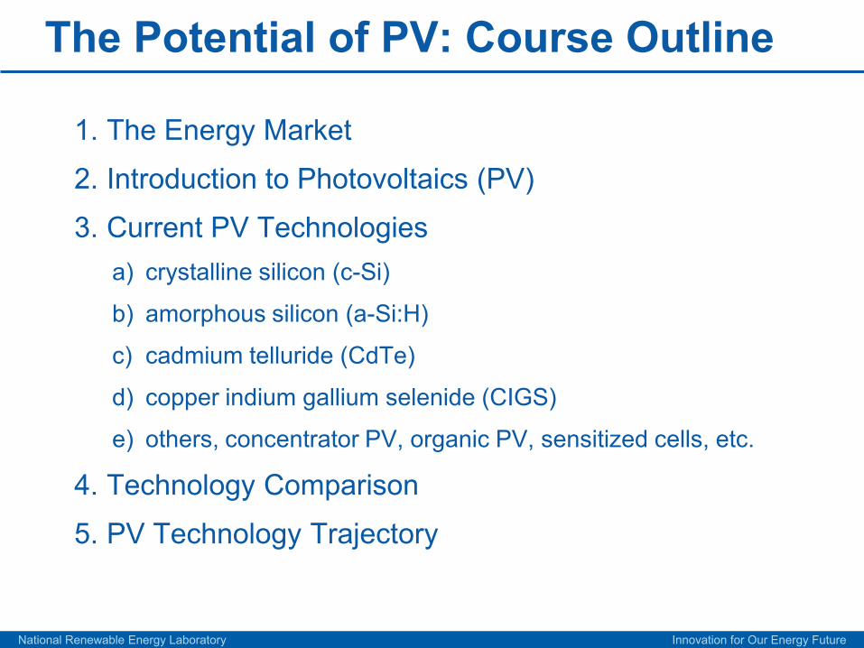
The Potential of PV: Course Outline
1. The Energy Market
2. Introduction to Photovoltaics (PV)
3. Current PV Technologiesa) crystalline silicon (c-Si)
b) amorphous silicon (a-Si:H)
c) cadmium telluride (CdTe)
d) copper indium gallium selenide (CIGS)
e) others, concentrator PV, organic PV, sensitized cells, etc.
4. Technology Comparison
5. PV Technology Trajectory
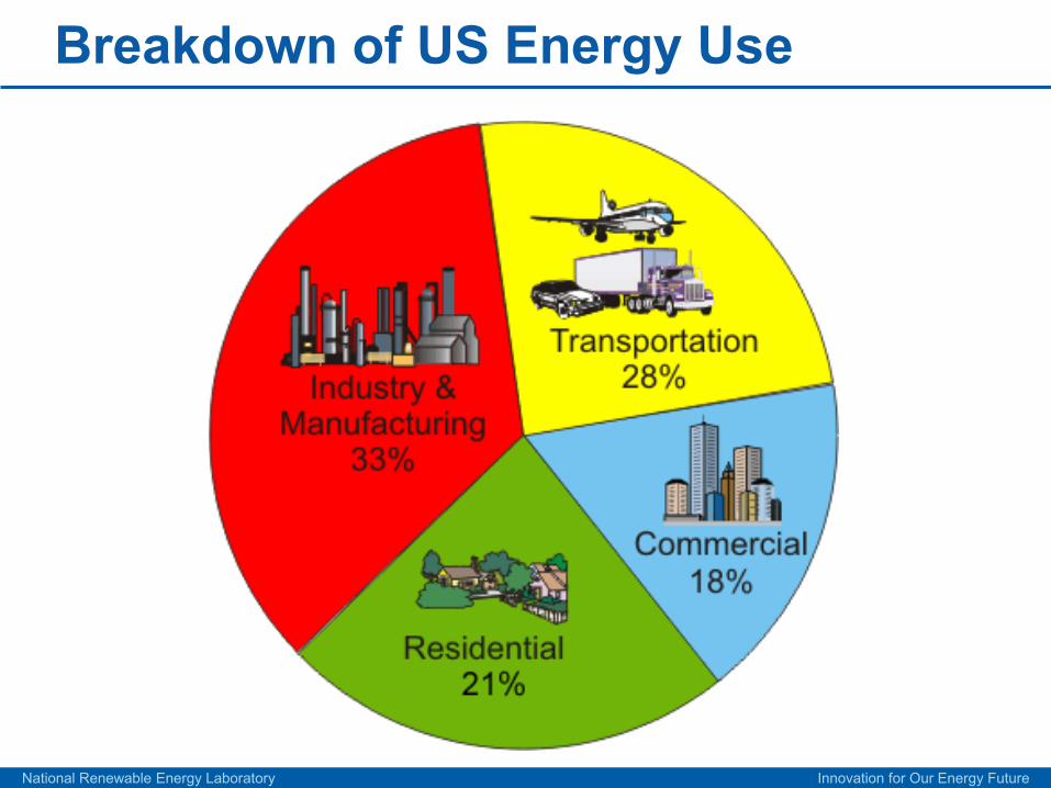
Breakdown of US Energy Use
National Renewable Energy Laboratory Innovation for Our Energy Future
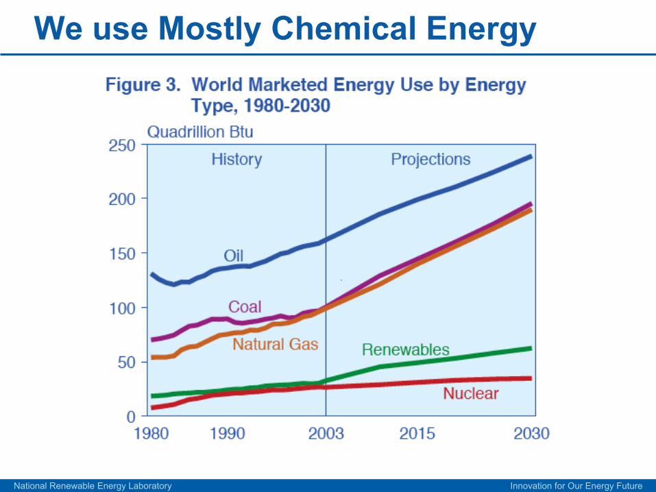
We use Mostly Chemical Energy
National Renewable Energy Laboratory Innovation for Our Energy Future
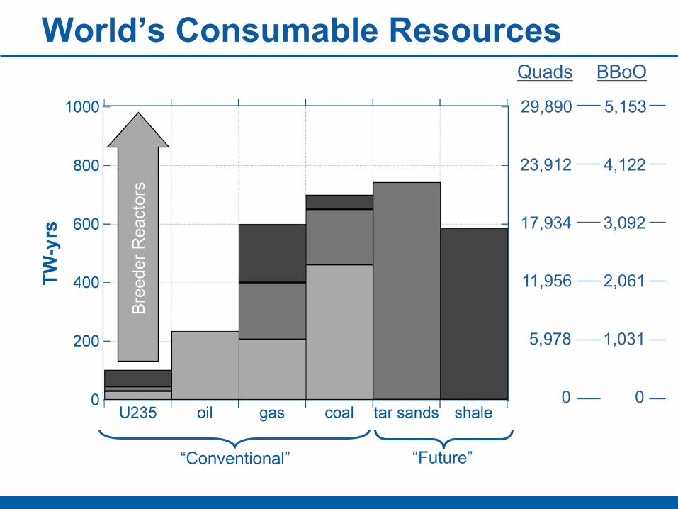
World’s Consumable Resources
Bre
eder
Rea
ctor
s
“Conventional” “Future”
0
5,978
11,956
17,934
23,912
29,890
0
1,031
2,061
3,092
4,122
5,153
Quads BBoO
40
30
20
10
0
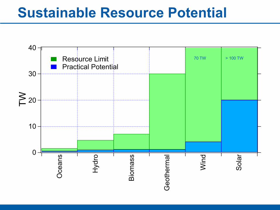
TW
Oce
ans
Hyd
ro
Bio
mas
s
Geo
ther
mal
Win
d
Sol
ar
Resource Limit Practical Potential
Sustainable Resource Potential
70 TW > 100 TW
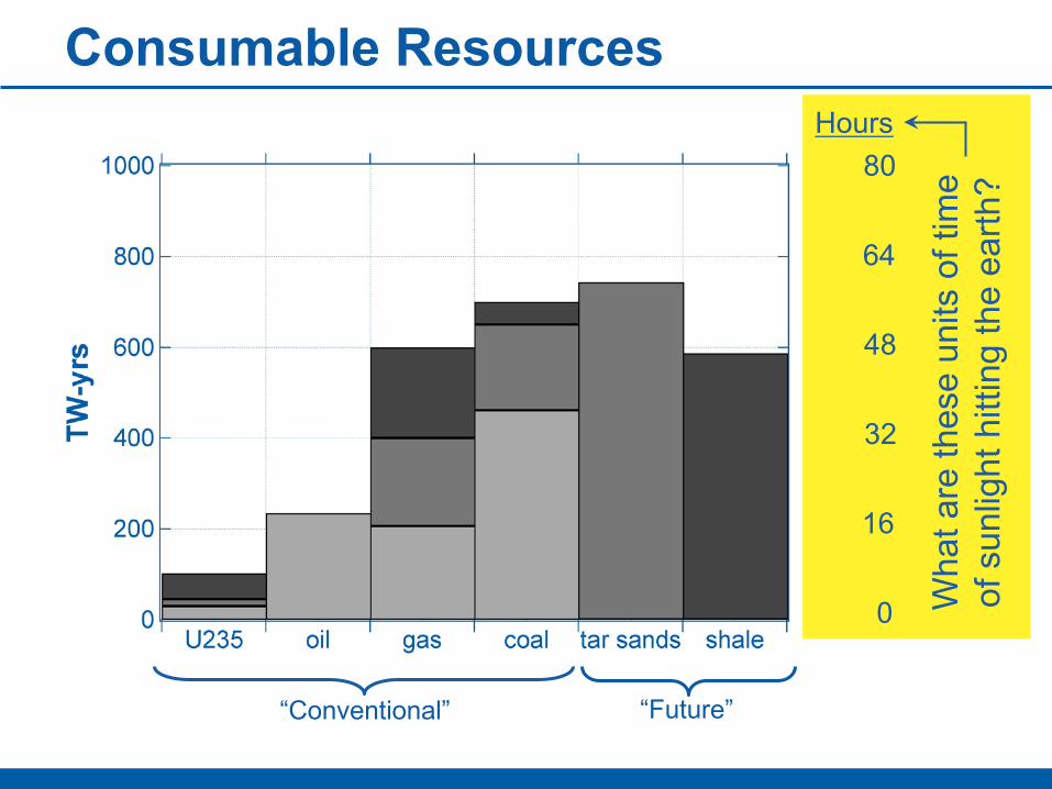
Consumable Resources
0
16
32
48
64
80
Wha
t are
thes
e un
its o
f tim
eof
sun
light
hitt
ing
the
earth
?
Hours
“Conventional” “Future”

Solar Energy Technologies
Passive Solar(space heating)
ConcentratingSolar Power
SolarHot Water
Solar Electric - Photovoltaics
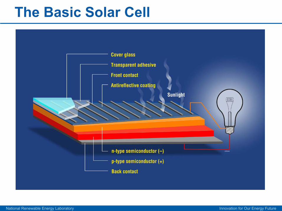
The Basic Solar Cell
National Renewable Energy Laboratory Innovation for Our Energy Future
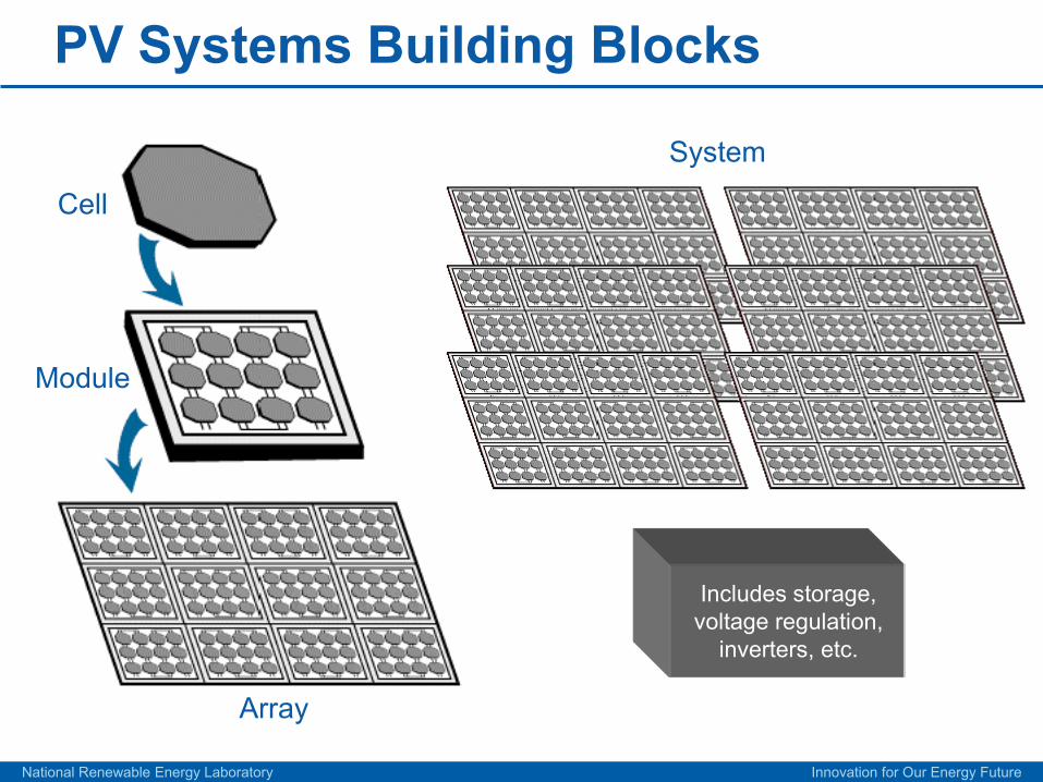
PV Systems Building Blocks
National Renewable Energy Laboratory Innovation for Our Energy Future
Cell
Module
Array
System
Includes storage,voltage regulation,
inverters, etc.
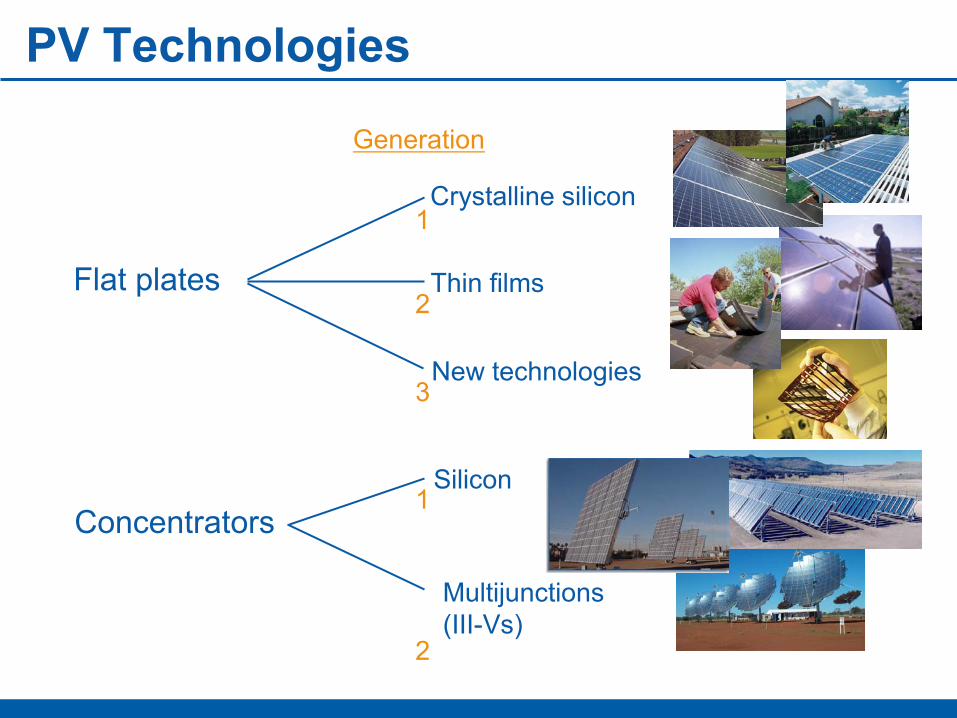
PV Technologies
ConcentratorsSilicon
Multijunctions(III-Vs)
Flat plates
Crystalline silicon
Thin films
New technologies
Generation
1
2
3
1
2
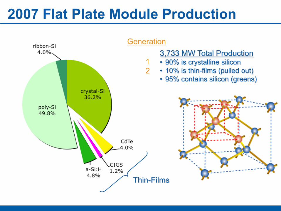
2007 Flat Plate Module Production
Thin-Films
3,733 MW Total Production• 90% is crystalline silicon• 10% is thin-films (pulled out)• 95% contains silicon (greens)
Source: Paul Maycock, PV News, February 2005
Generation
12
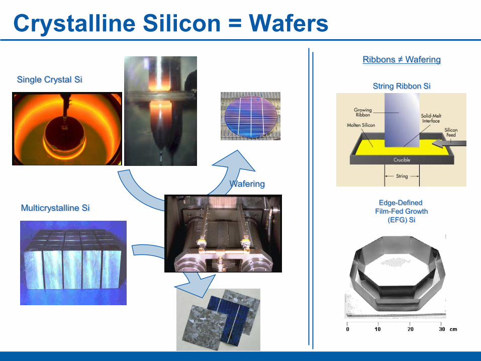
Crystalline Silicon = Wafers
Single Crystal Si
Multicrystalline Si
Wafering
Ribbons ≠ Wafering
String Ribbon Si
Edge-Defined Film-Fed Growth
(EFG) Si
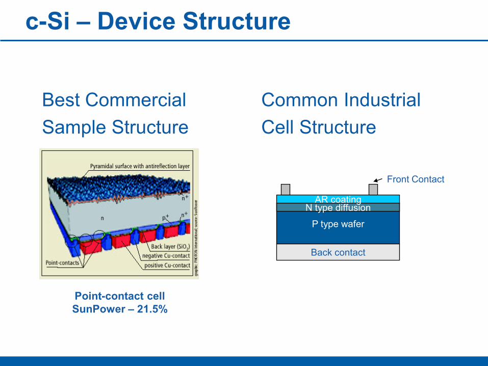
c-Si – Device Structure
Best CommercialSample Structure
Common IndustrialCell Structure
P type wafer
N type diffusionAR coating
Back contact
Front Contact
Point-contact cellSunPower – 21.5%
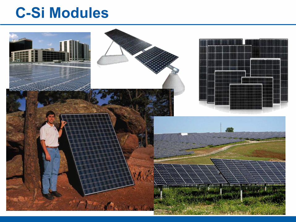
C-Si Modules
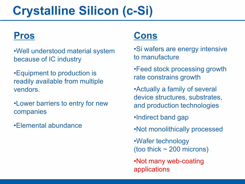
Crystalline Silicon (c-Si)
Pros•Well understood material system because of IC industry
•Equipment to production is readily available from multiple vendors.
•Lower barriers to entry for new companies
•Elemental abundance
Cons•Si wafers are energy intensive to manufacture
•Feed stock processing growth rate constrains growth
•Actually a family of several device structures, substrates, and production technologies
•Indirect band gap
•Not monolithically processed
•Wafer technology(too thick ~ 200 microns)
•Not many web-coating applications
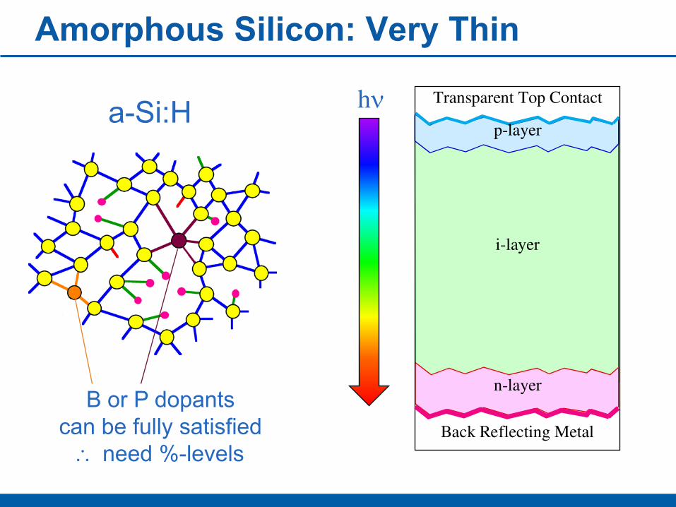
Amorphous Silicon: Very Thin
a-Si:H Transparent Top Contact
Back Reflecting Metal
p-layer
i-layer
n-layerB or P dopants
can be fully satisfied∴ need %-levels
hν
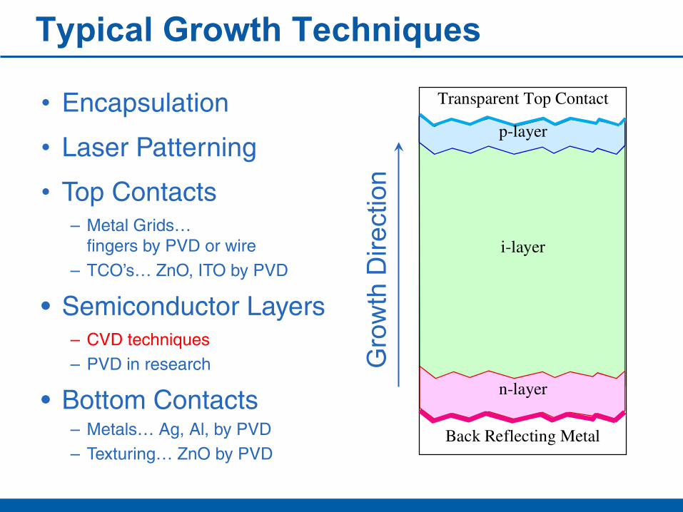
Typical Growth Techniques
Transparent Top Contact
Back Reflecting Metal
p-layer
i-layer
n-layer
• Encapsulation
• Laser Patterning
• Top Contacts– Metal Grids…
fingers by PVD or wire– TCO’s… ZnO, ITO by PVD
• Semiconductor Layers– CVD techniques– PVD in research
• Bottom Contacts– Metals… Ag, Al, by PVD– Texturing… ZnO by PVD
Gro
wth
Dire
ctio
n

a-Si:H Modules
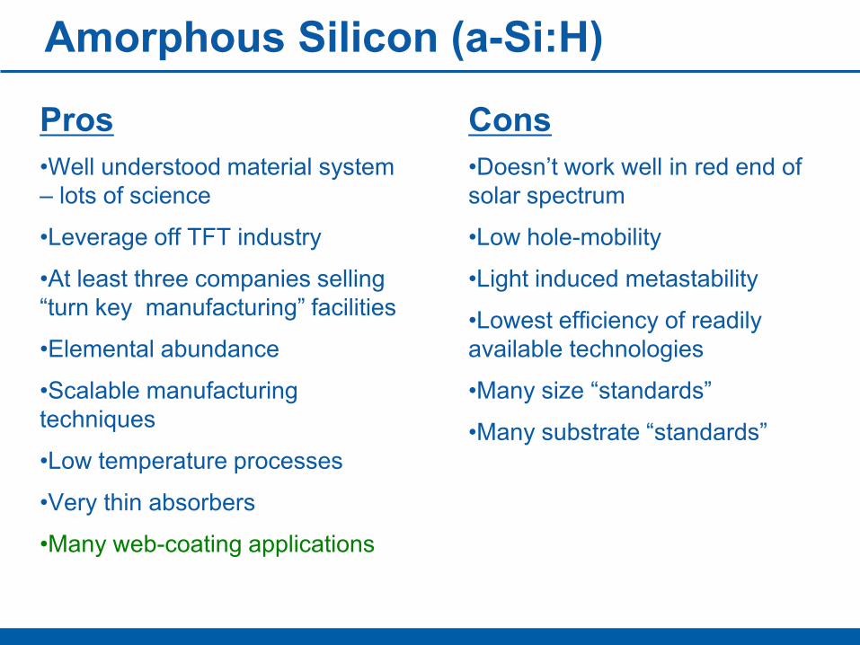
Amorphous Silicon (a-Si:H)
Pros•Well understood material system – lots of science
•Leverage off TFT industry
•At least three companies selling “turn key manufacturing” facilities
•Elemental abundance
•Scalable manufacturing techniques
•Low temperature processes
•Very thin absorbers
•Many web-coating applications
Cons•Doesn’t work well in red end of solar spectrum
•Low hole-mobility
•Light induced metastability
•Lowest efficiency of readily available technologies
•Many size “standards”
•Many substrate “standards”
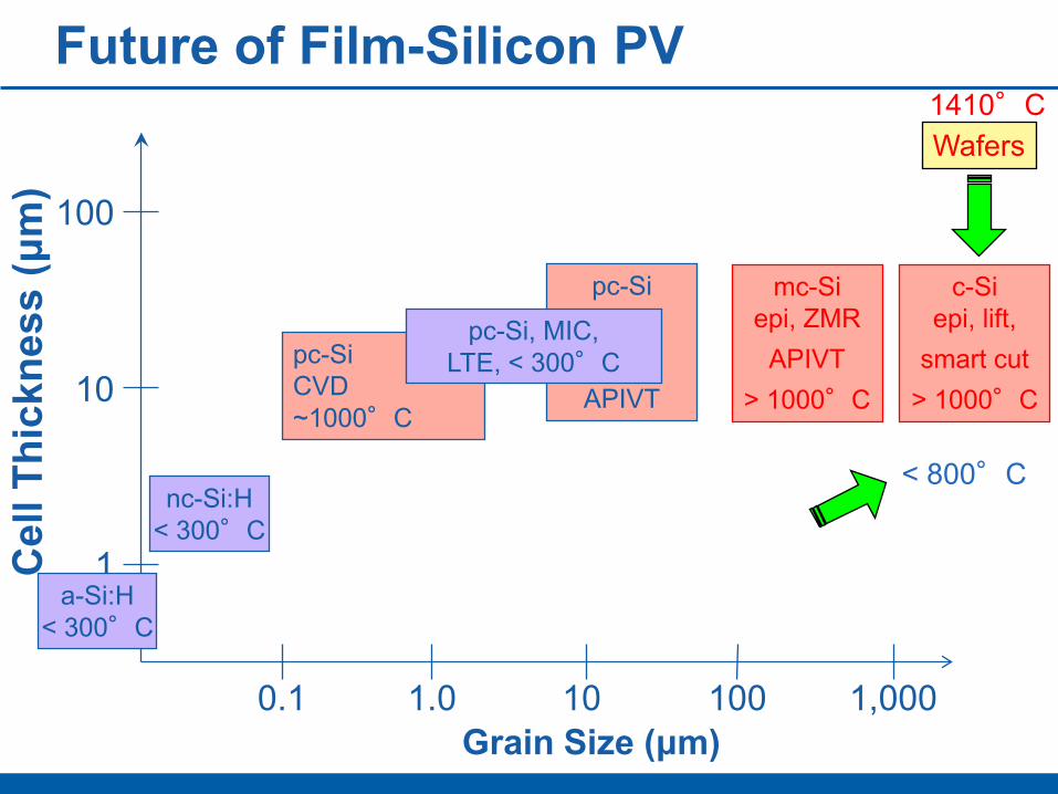
Future of Film-Silicon PV
0.1 1.0 10 100 1,000
10
100
nc-Si:H< 300°C
pc-Si
APIVT
pc-SiCVD~1000°C
pc-Si, MIC,LTE, < 300°C
mc-Siepi, ZMR
APIVT> 1000°C
c-Siepi, lift,
smart cut> 1000°C
1
Grain Size (μm)
Cel
l Thi
ckne
ss (μ
m)
Wafers
< 800°C
1410°C
a-Si:H< 300°C
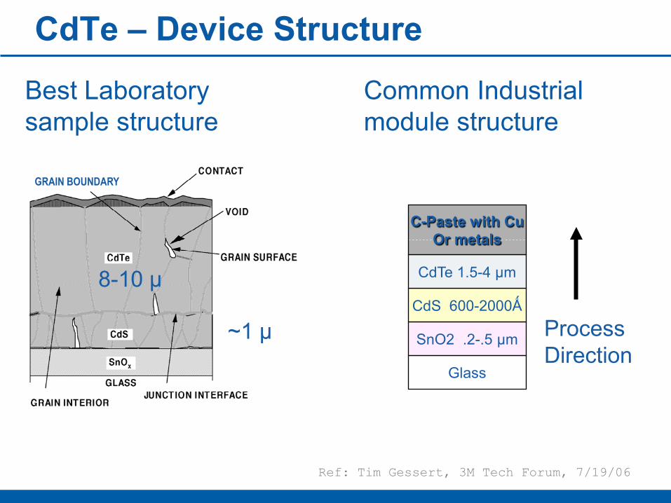
CdTe – Device Structure
Best Laboratory sample structure
Common Industrial module structure
~1 µ
8-10 µ
GRAIN BOUNDARY
Process Direction
Ref: Tim Gessert, 3M Tech Forum, 7/19/06
Glass
SnO2 .2-.5 µm
CdS 600-2000Ǻ
CdTe 1.5-4 µm
C-Paste with CuOr metals
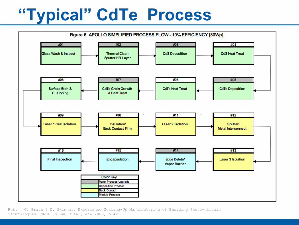
“Typical” CdTe Process
Ref: G. Braun & D. Skinner, Experience Scaling-Up Manufacturing of Emerging Photovolltaic Technologies, NREL SR-640-39165, Jan 2007, p 42

CdTe Modules
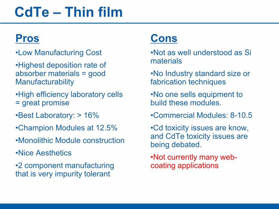
CdTe – Thin film
Pros•Low Manufacturing Cost•Highest deposition rate of absorber materials = good Manufacturability•High efficiency laboratory cells = great promise •Best Laboratory: > 16% •Champion Modules at 12.5%•Monolithic Module construction•Nice Aesthetics•2 component manufacturing that is very impurity tolerant
Cons •Not as well understood as Si materials•No Industry standard size or fabrication techniques•No one sells equipment to build these modules. •Commercial Modules: 8-10.5•Cd toxicity issues are know, and CdTe toxicity issues are being debated. •Not currently many web-coating applications
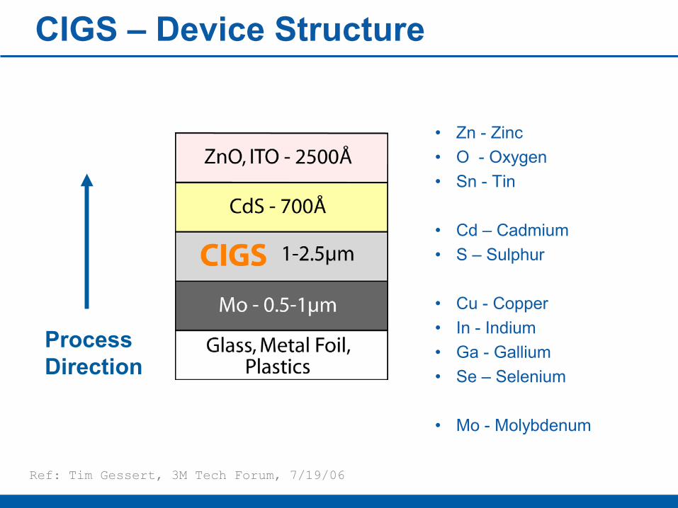
CIGS – Device Structure
Process Direction
Ref: Tim Gessert, 3M Tech Forum, 7/19/06
• Zn - Zinc• O - Oxygen• Sn - Tin
• Cd – Cadmium• S – Sulphur
• Cu - Copper• In - Indium• Ga - Gallium• Se – Selenium
• Mo - Molybdenum
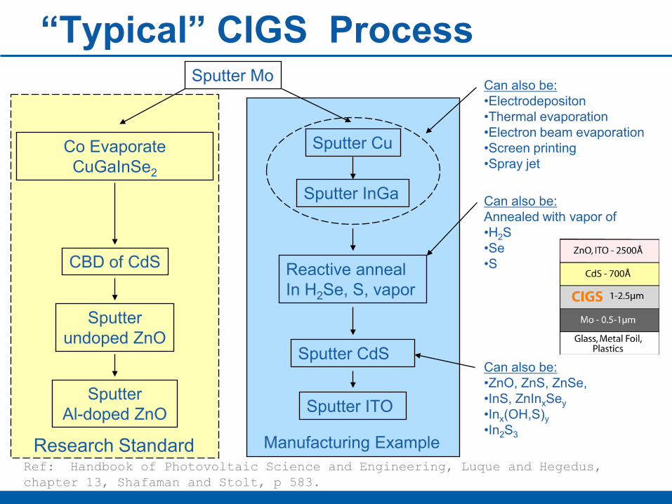
“Typical” CIGS ProcessSputter Mo
Co Evaporate CuGaInSe2
CBD of CdS
Sputterundoped ZnO
Sputter Cu
Reactive annealIn H2Se, S, vapor
Sputter InGa
Can also be:•Electrodepositon •Thermal evaporation•Electron beam evaporation•Screen printing•Spray jet
Ref: Handbook of Photovoltaic Science and Engineering, Luque and Hegedus,chapter 13, Shafaman and Stolt, p 583.
Sputter CdS
SputterAl-doped ZnO Sputter ITO
Can also be:•ZnO, ZnS, ZnSe,•InS, ZnInxSey•Inx(OH,S)y•In2S3
Can also be:Annealed with vapor of•H2S•Se•S
Research Standard Manufacturing Example
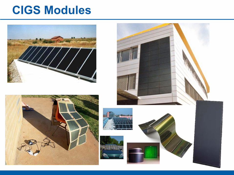
CIGS Modules
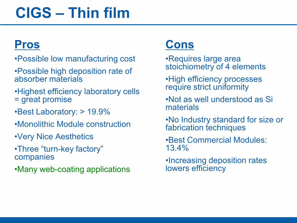
CIGS – Thin film
Pros•Possible low manufacturing cost•Possible high deposition rate of absorber materials•Highest efficiency laboratory cells = great promise •Best Laboratory: > 19.9% •Monolithic Module construction•Very Nice Aesthetics•Three “turn-key factory” companies•Many web-coating applications
Cons •Requires large area stoichiometry of 4 elements•High efficiency processes require strict uniformity•Not as well understood as Si materials•No Industry standard for size or fabrication techniques•Best Commercial Modules: 13.4%•Increasing deposition rates lowers efficiency
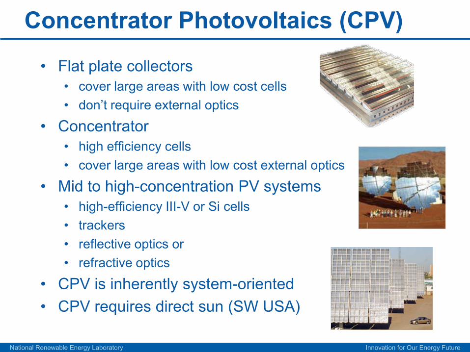
Concentrator Photovoltaics (CPV)
• Flat plate collectors• cover large areas with low cost cells• don’t require external optics
• Concentrator • high efficiency cells• cover large areas with low cost external optics
• Mid to high-concentration PV systems• high-efficiency III-V or Si cells• trackers• reflective optics or• refractive optics
• CPV is inherently system-oriented• CPV requires direct sun (SW USA)
National Renewable Energy Laboratory Innovation for Our Energy Future
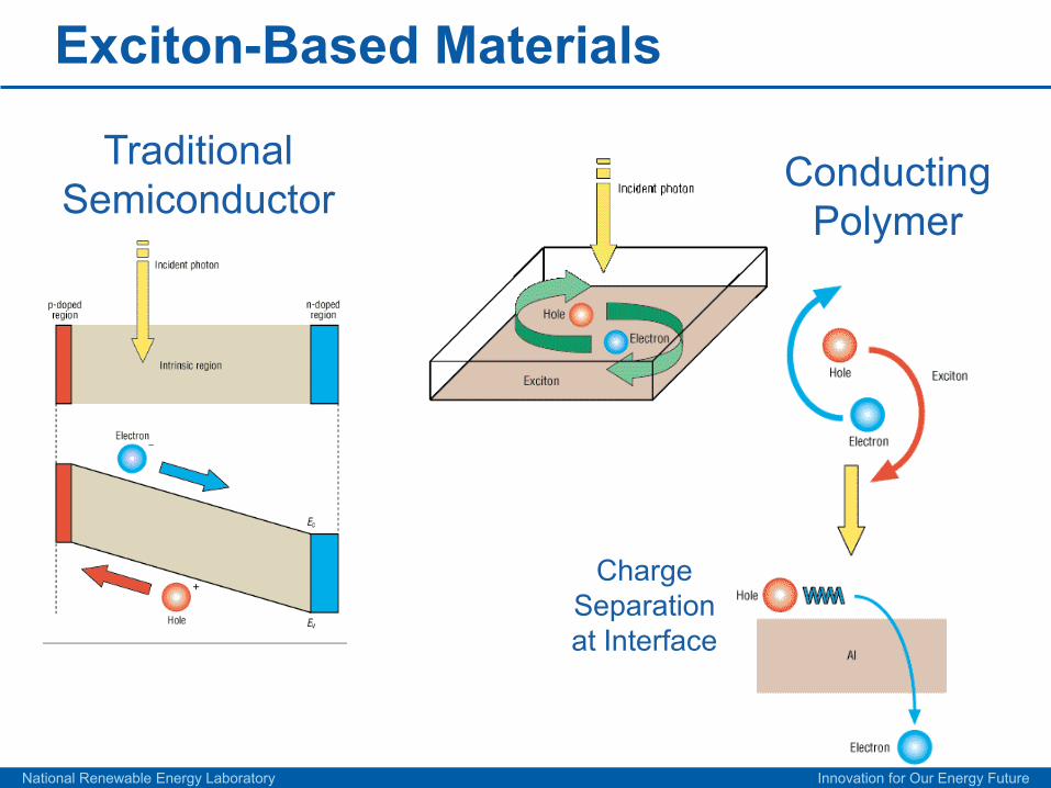
Exciton-Based Materials
National Renewable Energy Laboratory Innovation for Our Energy Future
TraditionalSemiconductor
ConductingPolymer
ChargeSeparationat Interface
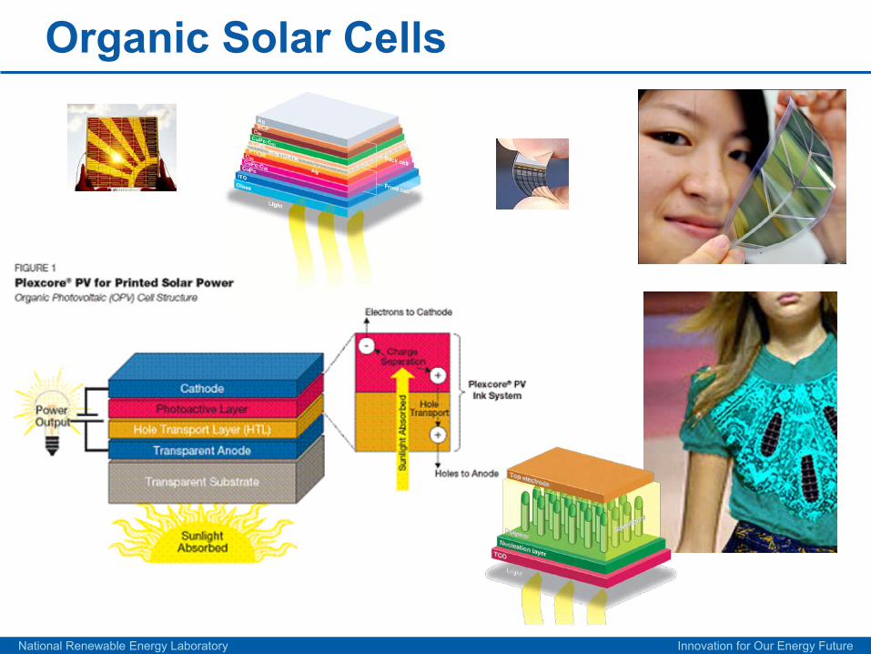
Organic Solar Cells
National Renewable Energy Laboratory Innovation for Our Energy Future

Grätzel (Dye-Sensitized) Cells
National Renewable Energy Laboratory Innovation for Our Energy Future
High surface areafor ruthenium-
polypyridine dye
Ox
Red
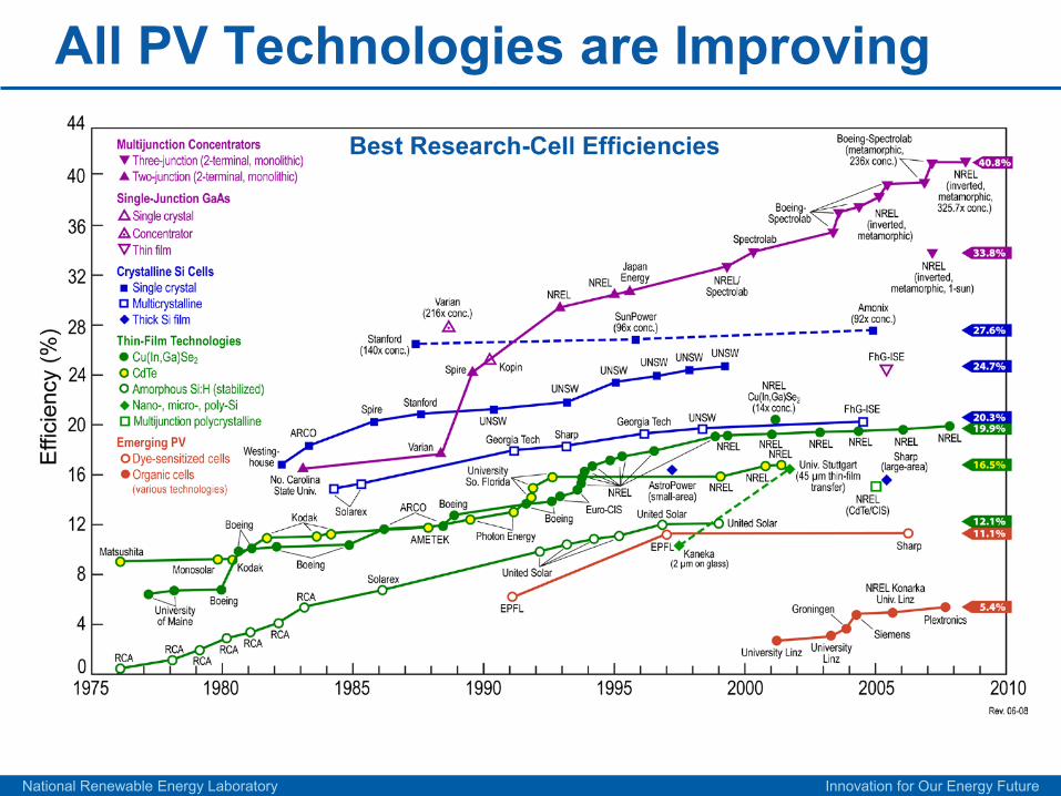
All PV Technologies are Improving
National Renewable Energy Laboratory Innovation for Our Energy Future
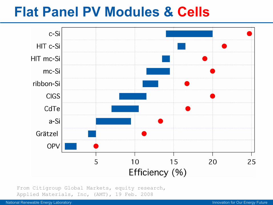
Flat Panel PV Modules & Cells
National Renewable Energy Laboratory Innovation for Our Energy Future
From Citigroup Global Markets, equity research,Applied Materials, Inc, (AMT), 19 Feb. 2008

Worldwide PV Module Production
National Renewable Energy Laboratory Innovation for Our Energy Future
Thin-Films
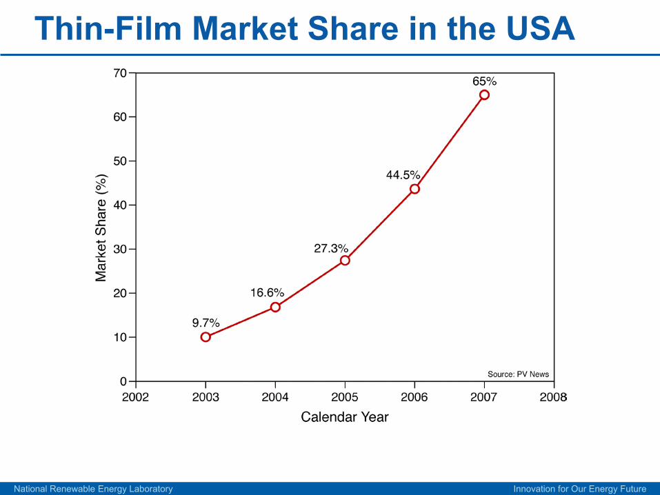
Thin-Film Market Share in the USA
National Renewable Energy Laboratory Innovation for Our Energy Future
National Renewable Energy Laboratory Innovation for Our Energy Future
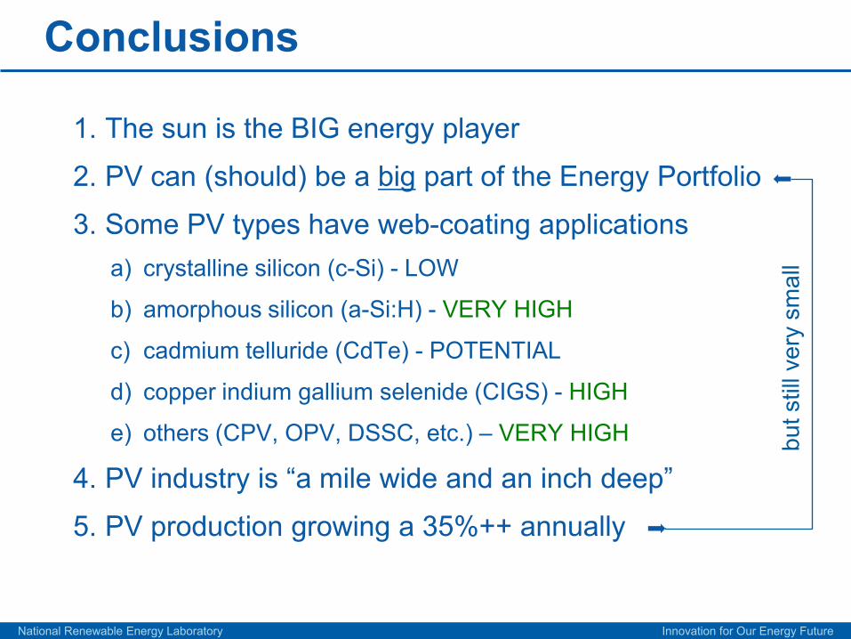
Conclusions
1. The sun is the BIG energy player
2. PV can (should) be a big part of the Energy Portfolio
3. Some PV types have web-coating applicationsa) crystalline silicon (c-Si) - LOW
b) amorphous silicon (a-Si:H) - VERY HIGH
c) cadmium telluride (CdTe) - POTENTIAL
d) copper indium gallium selenide (CIGS) - HIGH
e) others (CPV, OPV, DSSC, etc.) – VERY HIGH
4. PV industry is “a mile wide and an inch deep”
5. PV production growing a 35%++ annually
but s
till v
ery
smal
l