
Beyond Photovoltaics: Semiconductor Nanoarchitectures for ...
Upload
salvo-mirabellaCategory
view
461download
1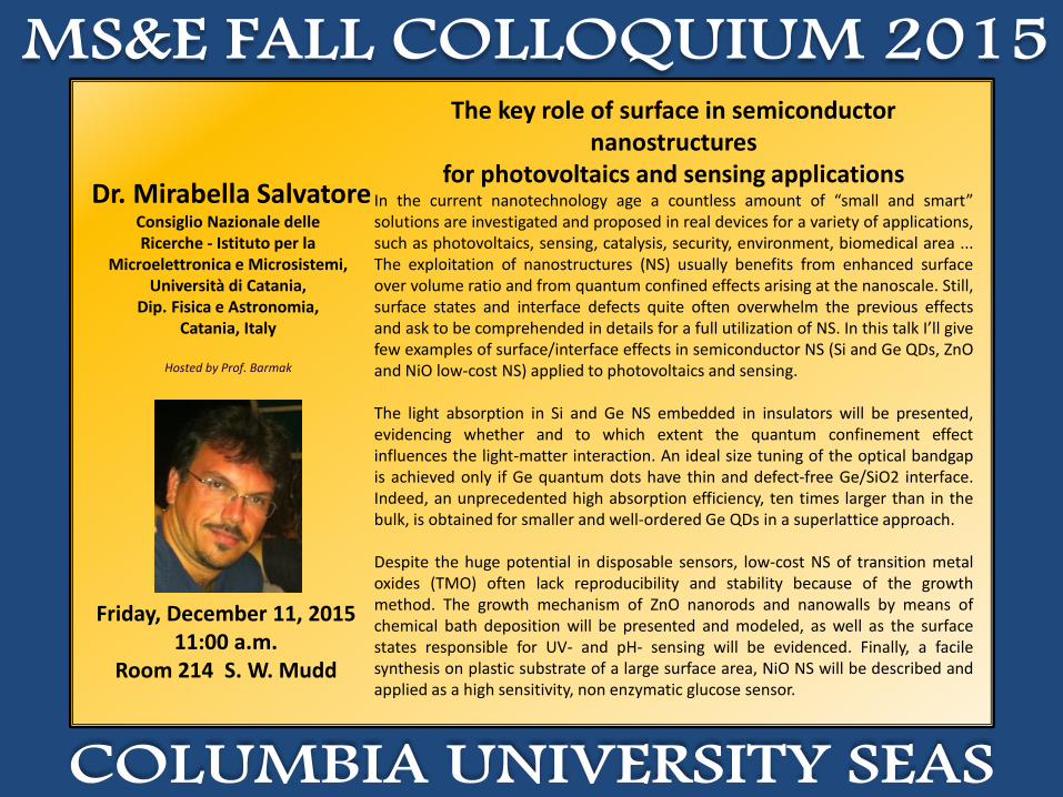
Dr. Mirabella SalvatoreConsiglio Nazionale delle Ricerche - Istituto per la
Microelettronica e Microsistemi,Università di Catania,
Dip. Fisica e Astronomia,Catania, Italy
Hosted by Prof. Barmak
The key role of surface in semiconductor nanostructures
for photovoltaics and sensing applicationsIn the current nanotechnology age a countless amount of “small and smart”solutions are investigated and proposed in real devices for a variety of applications,such as photovoltaics, sensing, catalysis, security, environment, biomedical area ...The exploitation of nanostructures (NS) usually benefits from enhanced surfaceover volume ratio and from quantum confined effects arising at the nanoscale. Still,surface states and interface defects quite often overwhelm the previous effectsand ask to be comprehended in details for a full utilization of NS. In this talk I’ll givefew examples of surface/interface effects in semiconductor NS (Si and Ge QDs, ZnOand NiO low-cost NS) applied to photovoltaics and sensing.
The light absorption in Si and Ge NS embedded in insulators will be presented,evidencing whether and to which extent the quantum confinement effectinfluences the light-matter interaction. An ideal size tuning of the optical bandgapis achieved only if Ge quantum dots have thin and defect-free Ge/SiO2 interface.Indeed, an unprecedented high absorption efficiency, ten times larger than in thebulk, is obtained for smaller and well-ordered Ge QDs in a superlattice approach.
Despite the huge potential in disposable sensors, low-cost NS of transition metaloxides (TMO) often lack reproducibility and stability because of the growthmethod. The growth mechanism of ZnO nanorods and nanowalls by means ofchemical bath deposition will be presented and modeled, as well as the surfacestates responsible for UV- and pH- sensing will be evidenced. Finally, a facilesynthesis on plastic substrate of a large surface area, NiO NS will be described andapplied as a high sensitivity, non enzymatic glucose sensor.
Friday, December 11, 201511:00 a.m.
Room 214 S. W. Mudd
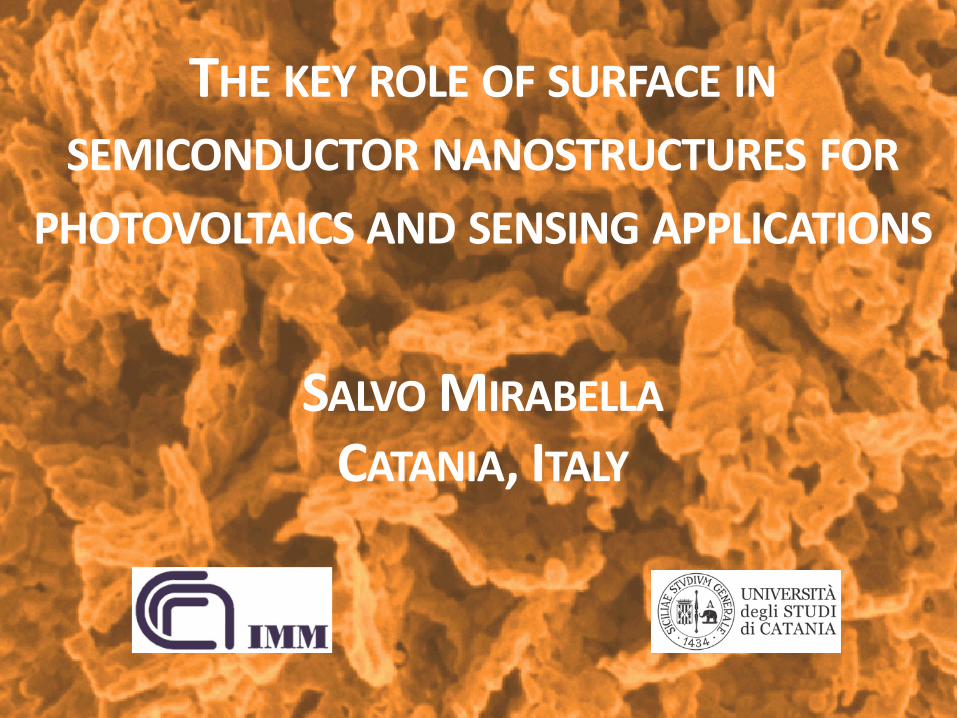
SALVO MIRABELLA CATANIA, ITALY
THE KEY ROLE OF SURFACE IN SEMICONDUCTOR NANOSTRUCTURES FOR
PHOTOVOLTAICS AND SENSING APPLICATIONS

Catania
J. DANCKERTS, XVII sec.
04 Dec. 2015

Columbia University, MSE colloquium, New York [email protected] 5/44
OUTLINE
0D
1D
2D
Ge QDs: not only size matters
ZnO NRs: surface defect engineering
ZnO NWs: flexible pH sensor NiO NF: flexible glucose sensor
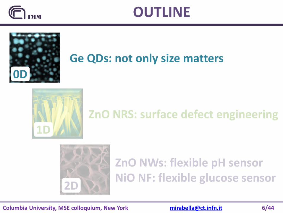
Columbia University, MSE colloquium, New York [email protected] 6/44
OUTLINE
0D
1D
2D
Ge QDs: not only size matters
ZnO NRS: surface defect engineering
ZnO NWs: flexible pH sensor NiO NF: flexible glucose sensor

Columbia University, MSE colloquium, New York [email protected] 7/44
Ge QDs for PV
Ge vs. Si • Higher absorption coefficient • Larger size range for QCE • Bandgap tuning within solar spectrum Si QDs
Ge QDs
Multi-junction SC All Si tandem solar cell “dream”

Columbia University, MSE colloquium, New York [email protected] 8/44
Light absorption in Ge QDs
S. Cosentino et al. APL (2011) P. Liu et al. JAP (2012) S. Mirabella et al. APL (2012) S. Cosentino et al. NRL (2013) S. Mirabella et al. APL (2013) S. Cosentino et al. JAP (2014) S. Cosentino et al. SOLMAT (2015) E. Barbagiovanni et al., JAP (2015) S. Cosentino et al., Nanoscale (2015)

Columbia University, MSE colloquium, New York [email protected] 9/44
Light absorption in Ge QDs
1 2 3 4 510-19
10-18
10-17
PECVD QDs (3.5 nm) PECVD QDs (4.4 nm) Sputter QDs (3 nm) Sputter QDs (4 nm)
Abso
rptio
n cr
oss
sect
ion
[cm
2 ]
Energy [eV]• Blue shift with decreasing QD size • Greater shift in PECVD w.r.t. sputter
Dtασ =
• Ge QDs (2-8 nm) embedded in SiO2 • Ge QDs density (~ 1018 cm-3) • Surface to surface (S2S) distance (1-3 nm)
absorption (α) absorption cross section (σ): photon absorption probability per Ge dose
SiGeO film
PECVD or sputter (deposition 250°C: 8 - 20% Ge)
(600-800°C annealing in N2)

Columbia University, MSE colloquium, New York [email protected] 10/44
Optical bandgap variation
2 4 6 8 10
1.0
1.5
2.0
2.5
3.0
QD size [nm]
PECVD Sputter a-Ge bulk
Opt
ical B
andg
ap [e
V]
2 4 6 8 10
1.0
1.5
2.0
2.5
3.0
QD size [nm]
PECVD Sputter a-Ge bulk
Opt
ical B
andg
ap [e
V]
• Eg vs size depends on synthesis technique … • Is there any role of interface ?
( ) ( )2optg
Tauc EB−⋅= ω
ωωα
Tauc law
VB
CB
VB
CB
Ge/SiO2 Ge/GeO2
V0,e 2.8 eV 1.2 eV
V0,h 4.5 eV 3.6 eV
2 4 6 8 10
1.0
1.5
2.0
2.5
3.0
QD size [nm]
PECVD Sputter a-Ge bulk EMA
Opt
ical B
andg
ap [e
V]
( )2
0*2*
22
21
2)(
−
+⋅+=
VmrLmbulkEQDE gg
π
• Eg vs size depends on synthesis technique … • Is there any role of interface ? • Any difference in the interfaces ?
SiO2 SiO2 Ge QD
SiO2 SiO2 Ge QD
GeO2

Columbia University, MSE colloquium, New York [email protected] 11/44
2 nm
Ge QD
TEM analysis
Z contrast profiling reveals systematically thinner interfaces in PECVD samples 2
1)(1)( 0 QDdiameterexf
xx≥Γ
+=
−Γ
−−
3.5 nm QD

Columbia University, MSE colloquium, New York [email protected] 12/44
EELS-STEM analysis
0.0
0.2
0.4
0.6
0.8
1.0
5 10 15 20 25 30 35 40 45 50 55 600.0
0.2
0.4
0.6
0.8
1.0
Sputter
Inte
nsity
[a.u
.]
PECVD
Inte
nsity
[a.u
.]
Energy [eV]
EELS core QD Fit
interband transition Ge Ge QD vol. plasmon SiO2 vol. plasmon Ge-Ge M4,5 band Ge-O M4,5 band
AGe-O
AGe-Ge
AGe-pl )( plGeGeGe
OGeOGe AA
AF−−
−− +
=
FGe-O ~ 16 % for sputter FGe-O ~ 8 % for PECVD
STEM: e-beam probe a cylinder of ~ 40 Ge atoms, 3 of which at surfaces
• Significant Ge-O surface contribution • Greater Ge-O contribution in sputter samples • Thinner interface in PECVD samples
e-beam
• How to consider these interfaces features in the QCE of Eg variation ?

Columbia University, MSE colloquium, New York [email protected] 13/44
SPDEM model
E. G. Barbagiovanni, et al., J. Appl. Phys. (2012), 111, 034307 E. G. Barbagiovanni, et al. Physica E, (2014), 63, 14–20 E. G. Barbagiovanni, et al., J. Appl. Phys. (2015), 117, 154304
Confining potential breaks the translational symmetry new momentum operator (pγ) effective mass spatially dependent
m(x)~1/(1+γx)2 γ~1/D as D decreases m(x) decreases confinement energy increases

Columbia University, MSE colloquium, New York [email protected] 14/44
Interface effect on bandgap
2 4 6 8 10
1.0
1.5
2.0
2.5
3.0
QD size [nm]
PECVD Sputter a-Ge bulk
Opt
ical B
andg
ap [e
V]
2 4 6 8 10
1.0
1.5
2.0
2.5
3.0
QD size [nm]
PECVD Sputter a-Ge bulk EMA
Opt
ical B
andg
ap [e
V]
2 4 6 8 10
1.0
1.5
2.0
2.5
3.0
QD size [nm]
PECVD Sputter a-Ge bulk EMA SPDEM PECVD SPDEM Sputter
Opt
ical B
andg
ap [e
V]
Ge/SiO2 Ge/GeO2 PECVD Sputter
V0,e 2.8 eV 1.2 eV 1.1 eV 0.9 eV
V0,h 4.5 eV 3.6 eV 3.3 eV 2.8 eV
( )( )
+
⋅+= *
,
,*,
,
23
hc
hc
ec
ecbulkgg m
VmV
DDEDE
µ
SPDEM model well accounts for the different Eg variation in the two samples
S. Cosentino, et al., Nanoscale (2015), 7, 11401
QD
SPDEM model

Columbia University, MSE colloquium, New York [email protected] 15/44
Ge QDs - conclusion
0D Ge QDs: not only size matters
Interface states affect the quantum confinement PECVD samples closer to ideal QCE (Ge/GeO2)
E. G. Barbagiovanni, et al., J. Appl. Phys. (2015), 117, 154304 S. Cosentino, et al., Nanoscale (2015), 7, 11401
2 4 6 8 10
1.0
1.5
2.0
2.5
3.0
QD size [nm]
PECVD Sputter a-Ge bulk EMA SPDEM PECVD SPDEM Sputter
Opt
ical B
andg
ap [e
V]
Columbia University, MSE colloquium, New York [email protected] 16/44
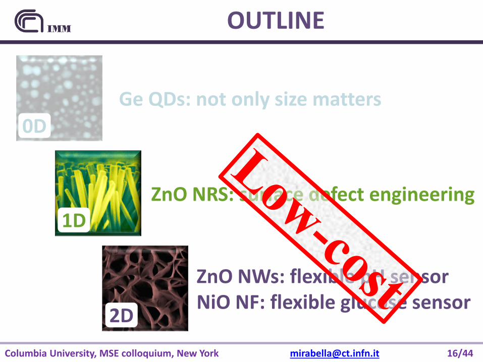
OUTLINE
0D
1D
2D
Ge QDs: not only size matters
ZnO NRS: surface defect engineering
ZnO NWs: flexible pH sensor NiO NF: flexible glucose sensor

Columbia University, MSE colloquium, New York [email protected] 17/44
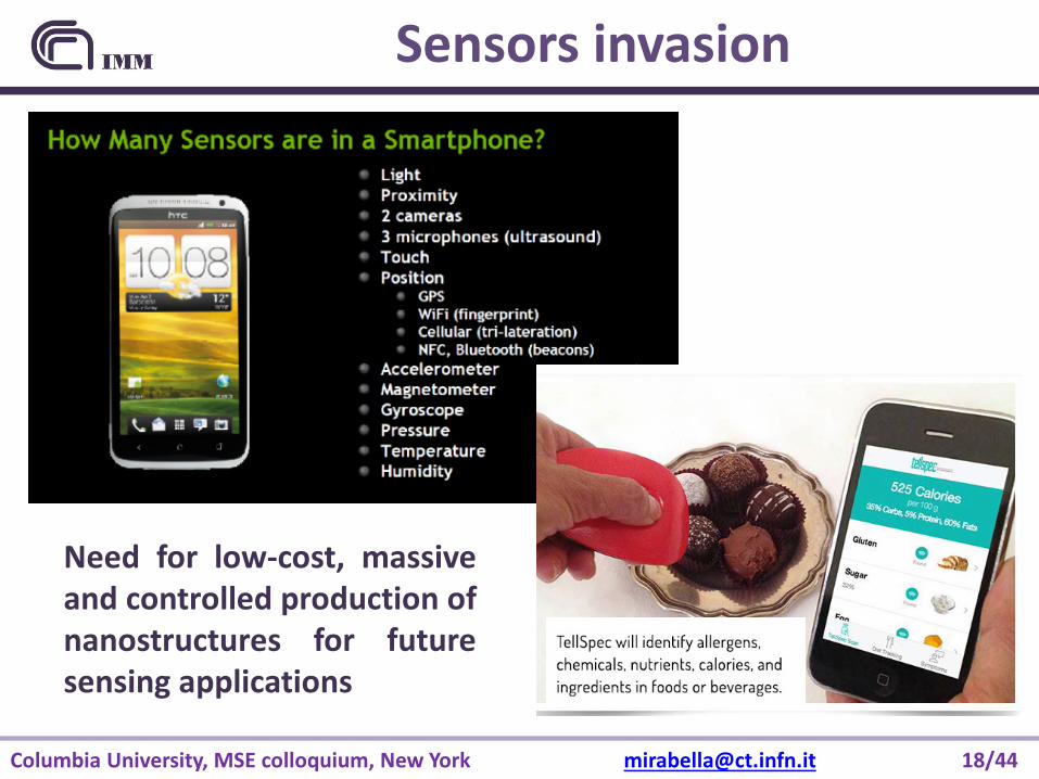
Global connections
Exponential growth of devices connected through IoT!
Columbia University, MSE colloquium, New York [email protected] 18/44
Sensors invasion
Need for low-cost, massive and controlled production of nanostructures for future sensing applications

Columbia University, MSE colloquium, New York [email protected] 19/44
OUTLINE
0D
1D
2D
Ge QDs: not only size matters
ZnO NRS: surface defect engineering
ZnO NWs: flexible pH sensor NiO NF: flexible glucose sensor
Columbia University, MSE colloquium, New York [email protected] 20/44
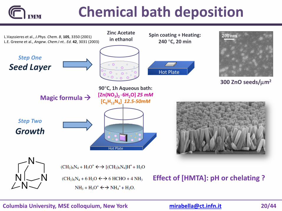
Step One
Seed Layer
Zinc Acetate in ethanol
Spin coating + Heating: 240 °C, 20 min
Hot Plate
Step Two Growth
90°C, 1h Aqueous bath: [Zn(NO3)2 ⋅6H2O] 25 mM
[C6H12N4] 12.5-50mM
L.Vayssieres et al., J.Phys. Chem. B, 105, 3350 (2001) L.E. Greene et al., Angew. Chem.I nt.. Ed. 42, 3031 (2003)
Chemical bath deposition
Effect of [HMTA]: pH or chelating ?
300 ZnO seeds/µm2
Hot Plate
Magic formula
Columbia University, MSE colloquium, New York [email protected] 22/44
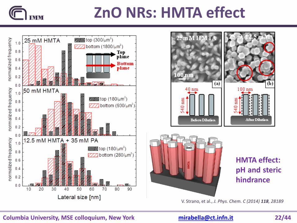
ZnO NRs: HMTA effect
V. Strano, et al., J. Phys. Chem. C (2014) 118, 28189
HMTA effect: pH and steric hindrance

Columbia University, MSE colloquium, New York [email protected] 23/44
Laser irradiation of ZnO NRs Adrian M. Chitu, prof. J. Im’s group - CU G. Fiaschi, Y. Komen, Y. Shacham – TAU Laser energy flux: 100-1000 mJ/cm2
950 770 550 225 mJ/cm2

Columbia University, MSE colloquium, New York [email protected] 24/44
Laser irradiation of ZnO NRs
580 mJ/cm2
310 mJ/cm2
Progressive melting from the top

Columbia University, MSE colloquium, New York [email protected] 25/44
ZnO NRs and light
Below gap light
Above gap light
Light emission
Light scattering
V. Strano, et al., Appl. Phys. Lett. (2015)
E. G. Barbagiovanni, et al., Nanoscale (2015)
Columbia University, MSE colloquium, New York [email protected] 26/44
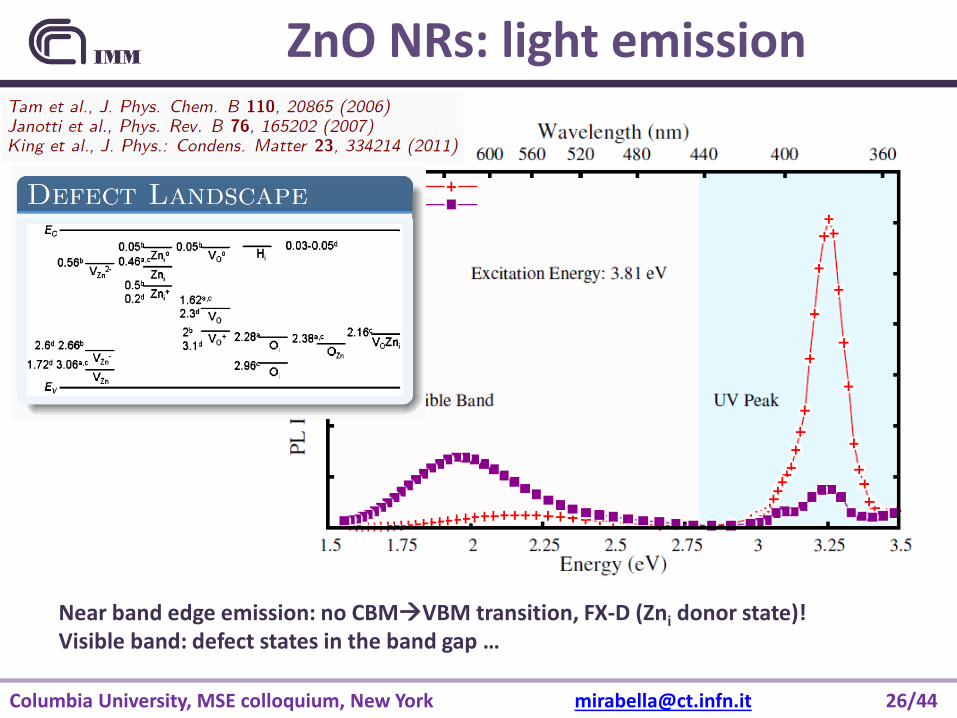
ZnO NRs: light emission
Near band edge emission: no CBMVBM transition, FX-D (Zni donor state)! Visible band: defect states in the band gap …
Columbia University, MSE colloquium, New York [email protected] 27/44
Defect engineering
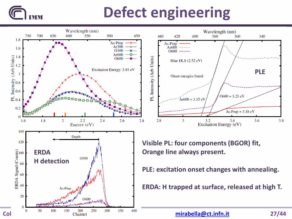
ERDA H detection
PLE
Visible PL: four components (BGOR) fit, Orange line always present. PLE: excitation onset changes with annealing. ERDA: H trapped at surface, released at high T.

Columbia University, MSE colloquium, New York [email protected] 28/44
BGOR model
E. G. Barbagiovanni, et al., Nanoscale (2015)
Surface defect engineering allows modulation of visible PL in ZnO nanorods
Columbia University, MSE colloquium, New York [email protected] 29/44
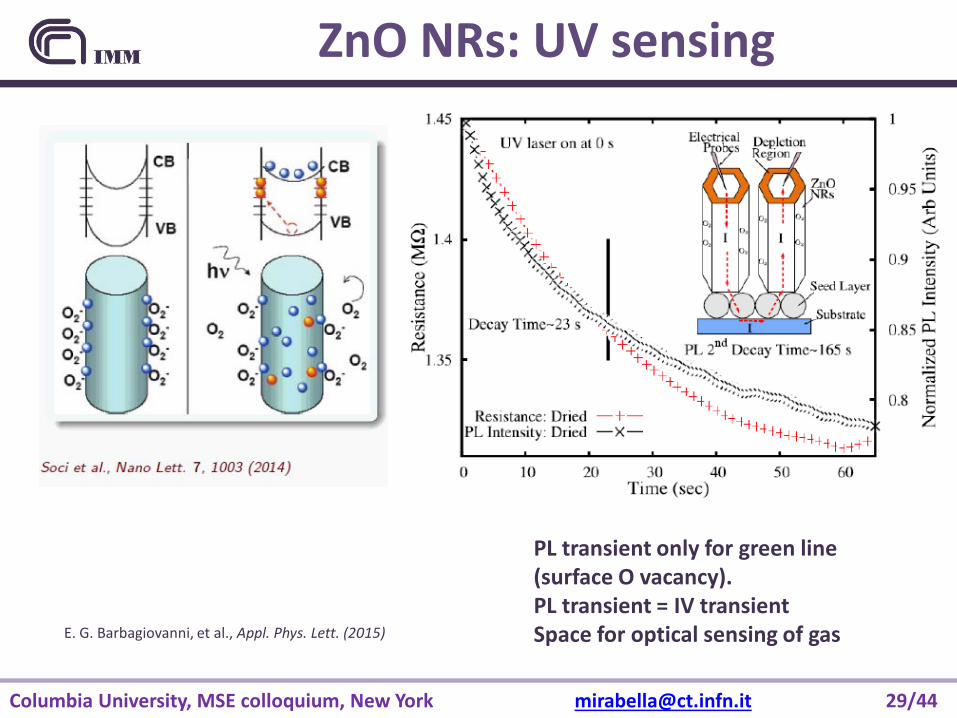
ZnO NRs: UV sensing
E. G. Barbagiovanni, et al., Appl. Phys. Lett. (2015)
PL transient only for green line (surface O vacancy). PL transient = IV transient Space for optical sensing of gas

Columbia University, MSE colloquium, New York [email protected] 30/44
ZnO NRs - conclusion
1D ZnO NRS: surface defect engineering
Low-cost but controlled ZnO NR synthesis (HMTA role) Laser annealing induced modification Surface defect engineering for sensing
V. Strano, et al., J. Phys. Chem. C (2014) V. Strano, et al., Appl. Phys. Lett. (2015) E. G. Barbagiovanni, et al., Nanoscale (2015)
E. G. Barbagiovanni, et al., Appl. Phys. Lett. (2015)

Columbia University, MSE colloquium, New York [email protected] 31/44
OUTLINE
0D
1D
2D
Ge QDs: not only size matters
ZnO NRS: surface defect engineering
ZnO NWs: flexible pH sensor NiO NF: flexible glucose sensor
Columbia University, MSE colloquium, New York [email protected] 32/44
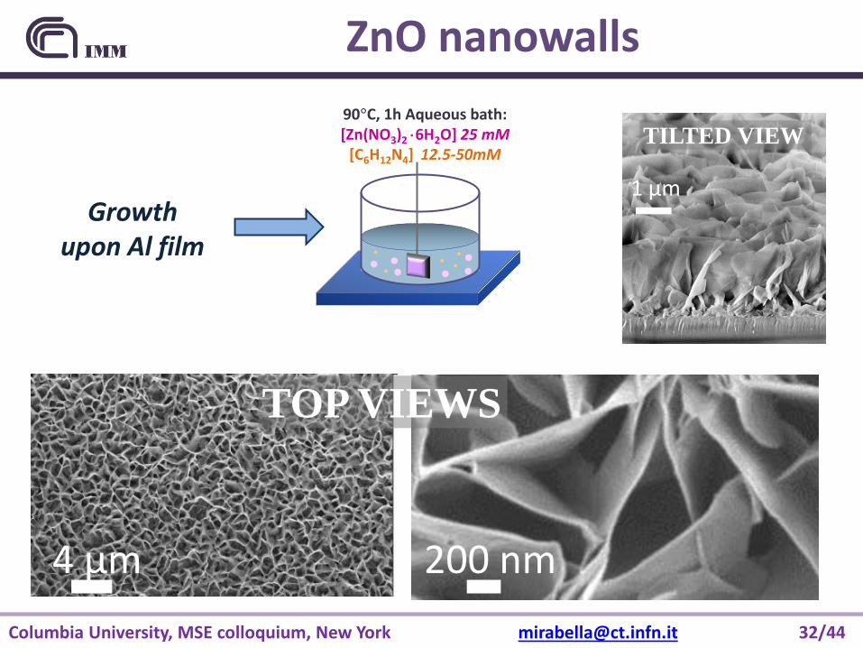
ZnO nanowalls
Growth upon Al film
90°C, 1h Aqueous bath: [Zn(NO3)2 ⋅6H2O] 25 mM
[C6H12N4] 12.5-50mM
4 µm
TOP VIEWS
200 nm
1 µm
TILTED VIEW

Columbia University, MSE colloquium, New York [email protected] 33/44
ZnO NWs: growth A
l(OH
) 4-
Al(O
H) 4
-
Al(O
H) 4
-
Substrate Al
Substrate Al
Substrate Al
Growth Time
φ s
K. O. Iwu, et al., Cryst. Growth Des. (2015)
Columbia University, MSE colloquium, New York [email protected] 34/44
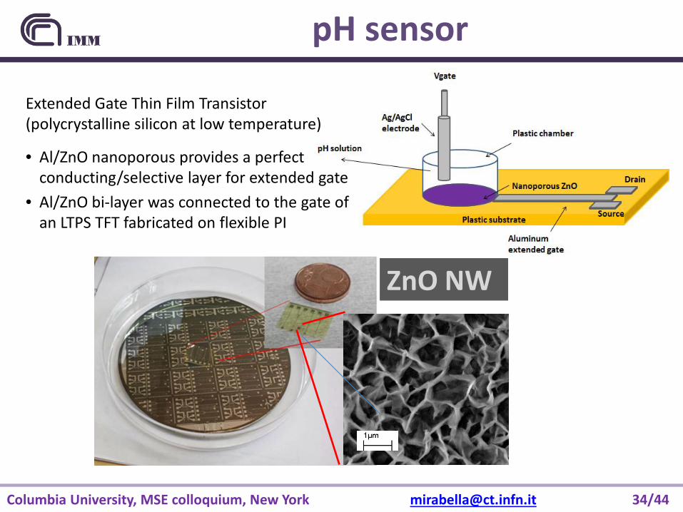
• Al/ZnO nanoporous provides a perfect conducting/selective layer for extended gate
• Al/ZnO bi-layer was connected to the gate of an LTPS TFT fabricated on flexible PI
pH sensor
Extended Gate Thin Film Transistor (polycrystalline silicon at low temperature)
ZnO NW

Columbia University, MSE colloquium, New York [email protected] 35/44
pH sensor
Basic test for further biosensors (as Enzyme FET) involving pH variation due to Enzyme-Analite reaction
- Measurements were performed @ 25 °C in dark condition and after 10 min after changing pH solution
- Reference electrode Ag/AgCl - IdVg performed @ Vds=0.1 V with slow ramp rate (2 s/V) - IdVds performed @ Vg=9 V
- pH-sensitivity nearly 60 mV/pH, close to ideal
Nernstian response (2.3 KT=60 mV/pH)) L. Maiolo, et al., Appl. Phys. Lett. (2014)
Columbia University, MSE colloquium, New York [email protected] 36/44
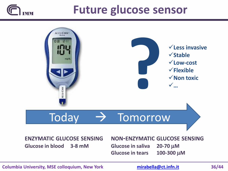
Future glucose sensor
Today Tomorrow
Less invasive Stable Low-cost Flexible Non toxic …
NON-ENZYMATIC GLUCOSE SENSING Glucose in saliva 20-70 µM Glucose in tears 100-300 µM
ENZYMATIC GLUCOSE SENSING Glucose in blood 3-8 mM
Columbia University, MSE colloquium, New York [email protected] 37/44
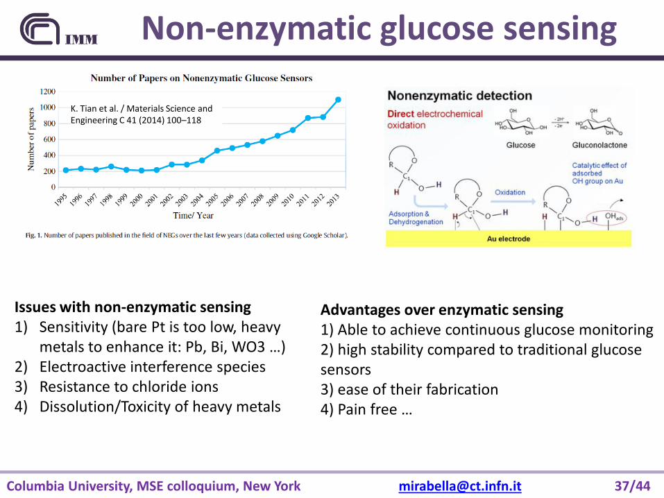
Non-enzymatic glucose sensing
Issues with non-enzymatic sensing 1) Sensitivity (bare Pt is too low, heavy
metals to enhance it: Pb, Bi, WO3 …) 2) Electroactive interference species 3) Resistance to chloride ions 4) Dissolution/Toxicity of heavy metals
Advantages over enzymatic sensing 1) Able to achieve continuous glucose monitoring 2) high stability compared to traditional glucose sensors 3) ease of their fabrication 4) Pain free …
K. Tian et al. / Materials Science and Engineering C 41 (2014) 100–118

Columbia University, MSE colloquium, New York [email protected] 38/44
Chemical bath deposition
Ingredients: 1) Nickel sulfate hexahydrate 2) potassium persulfate 3) ammonia solution Mix at room temperature Substrate: FTO or ITO covered UPILEX Immersion time: 5 minutes
Ni(OH)2 nanosheets
650
nm
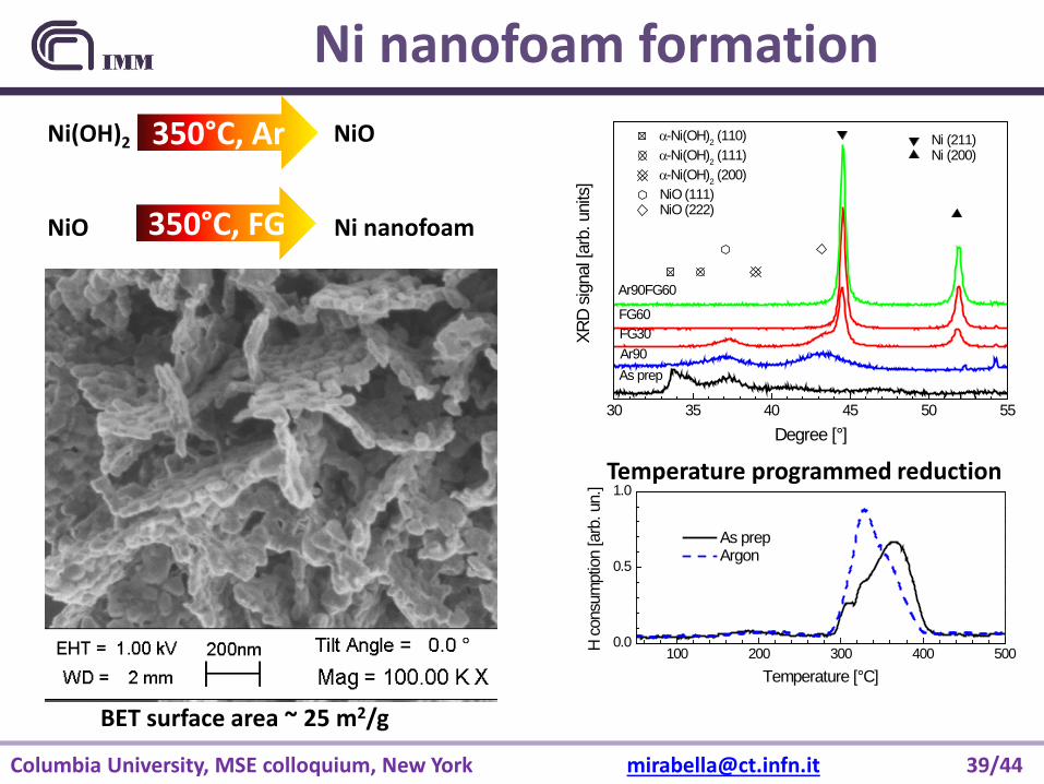
Columbia University, MSE colloquium, New York [email protected] 39/44
30 35 40 45 50 55
Ni (211) Ni (200)
Ar90FG60
FG60FG30Ar90
α-Ni(OH)2 (110) α-Ni(OH)2 (111) α-Ni(OH)2 (200) NiO (111) NiO (222)
XRD
signa
l [ar
b. u
nits
]
Degree [°]
As prep
Ni nanofoam formation
100 200 300 400 5000.0
0.5
1.0
H co
nsum
ptio
n [a
rb. u
n.]
Temperature [°C]
As prep Argon
Temperature programmed reduction
BET surface area ~ 25 m2/g
Ni(OH)2 NiO NiO Ni nanofoam
350°C, Ar
350°C, FG
Columbia University, MSE colloquium, New York [email protected] 40/44
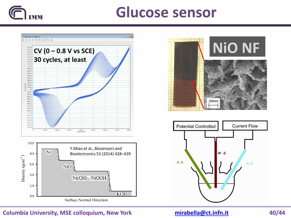
Glucose sensor
CV (0 – 0.8 V vs SCE) 30 cycles, at least
Y.Miao et al., Biosensors and Bioelectronics 53 (2014) 428–439
NiO NF
Columbia University, MSE colloquium, New York [email protected] 41/44
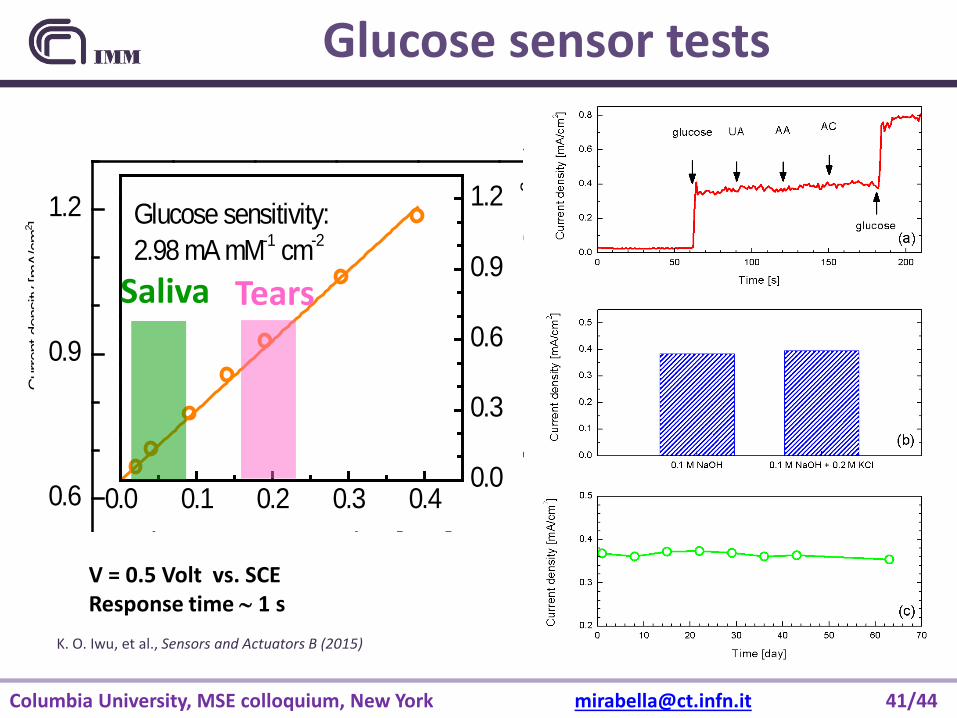
Glucose sensor tests
0 100 2000.0
0.3
0.6
0.9
1.2
50 µM
Cur
rent
den
sity
[mA/
cm2 ]
Time [s]
Ni nanofoam on FTO glass
20 µM
100 µM
0.0 0.1 0.2 0.3 0.40.0
0.3
0.6
0.9
1.2
cur
rent
den
sity
[mA/
cm2 ]
Glucose concentration [mM]
Glucose sensitivity:2.98 mA mM-1 cm-2
V = 0.5 Volt vs. SCE Response time ∼ 1 s
0.6
0.9
1.2
0.0 0.1 0.2 0.3 0.40.0
0.3
0.6
0.9
1.2
2
Gl t ti [ M]
Glucose sensitivity:2.98 mA mM-1 cm-2
Tears Saliva
K. O. Iwu, et al., Sensors and Actuators B (2015)

Columbia University, MSE colloquium, New York [email protected] 42/44
2D - conclusion
2D
ZnO NWs: flexible pH sensor NiO NF: flexible glucose sensor
Controlled, inexpensive growth of large surface area material ZnO NWs as ideal sensing nanostructure for pH NiO NF for non-enzymatic, high sensitivity glucose sensing
L. Maiolo, et al., Appl. Phys. Lett. (2014)
K. O. Iwu, et al., Cryst. Growth Des. (2015) K. O. Iwu, et al., Sensors and Actuators B (2015)
Columbia University, MSE colloquium, New York [email protected] 43/44
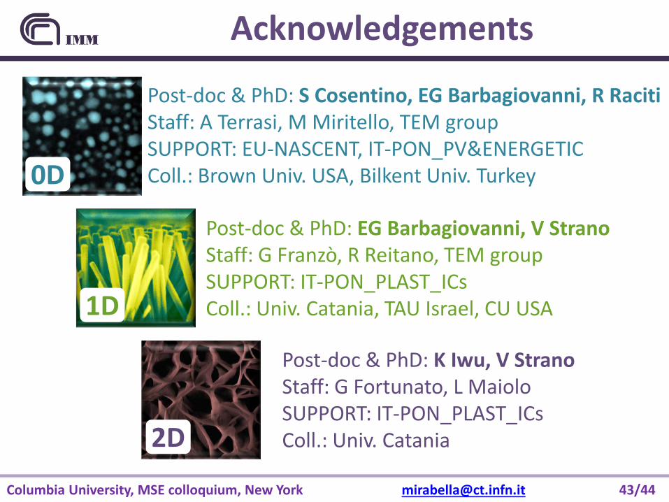
Acknowledgements
0D
1D
2D
Post-doc & PhD: S Cosentino, EG Barbagiovanni, R Raciti Staff: A Terrasi, M Miritello, TEM group SUPPORT: EU-NASCENT, IT-PON_PV&ENERGETIC Coll.: Brown Univ. USA, Bilkent Univ. Turkey
Post-doc & PhD: EG Barbagiovanni, V Strano Staff: G Franzò, R Reitano, TEM group SUPPORT: IT-PON_PLAST_ICs Coll.: Univ. Catania, TAU Israel, CU USA
Post-doc & PhD: K Iwu, V Strano Staff: G Fortunato, L Maiolo SUPPORT: IT-PON_PLAST_ICs Coll.: Univ. Catania