Hierarchical nanostructures for light management in thin-film optoelectronic devices by Seyed
Hierarchical Semiconductor, Metal and Hybrid Nanostructures and the Study of their Light-Matter
Interactions
By
Anna Lee
A thesis submitted in conformity with the requirements for the degree of Doctor of Philosophy
Graduate Department of Chemistry University of Toronto
© Copyright by Anna Lee, 2012

ii
Hierarchical Semiconductor, Metal and Hybrid Nanostructures and
the Study of their Light-Matter Interactions
Anna Lee
Doctor of Philosophy
Graduate Department of Chemistry
University of Toronto
2012
Abstract
The work presented in this thesis explores the optical properties of hierarchical structures
composed of nanoscale building blocks ranging from metals to semiconductors and
composites, organized through bottom-up design methods.
1) By following the dynamic generation of hot-spots in self-assembled chains of gold
nanorods (NRs), we have established a direct correlation between ensemble-averaged
surface-enhanced Raman scattering (SERS) and extinction properties of these nanoscale
chains. Experimental results were supported by comprehensive finite-difference time-
domain simulations (FDTD). The relationship established between the structure of nanorod
ensembles and their optical properties provides a basis for producing dynamic, solution-
based, plasmonic platforms for applications ranging from sensing to nanoelectronics.
2) We report theoretical and experimental analyses of the optical properties of
side-by-side assembled gold NRs. Comprehensive FDTD simulations showed a blue shift of
the surface plasmon resonance in the side-by-side assembled NR structures and a
reduction of electric field intensity as the number of NRs per stack increased. These results
iii
were experimentally verified via extinction measurements and ensemble-averaged SERS
spectroscopy. The experimental results and electrodynamic simulations were found to be
in agreement.
3) The efficacy of hollow core photonic crystal fibers (HCPCF) as a platform for SERS
spectroscopy was demonstrated. SERS measurements carried out using this platform
showed the capability to monitor minute amounts of ligands on the surface of gold
nanoparticles and SERS signals from HCPCF exhibited a 10-fold enhancement. Using the
exchange of cetyltrimethylammonium bromide with α-methoxy-ω mercaptopolyethylene
glycol on the surface of gold nanorods as an exemplary system, we showed the feasibility of
using HCPCF SERS to monitor the change in surface chemistry of NRs.
4) Facile, solution-phase formation of ordered, lamellar quantum dot (QD) arrays
exhibiting structural integrity and temporal stability, without the need for chemical
crosslinking, was achieved. While micrometers in diameter, they are typically only two to
three QD layers thick. These structures are capable of carrying a cargo of water-soluble
ions, molecules, metal nanoparticles, or biomolecules. The photoluminescence of the host
CdSe QDs were enhanced by the encapsulation of gold nanoparticles within the lamellae,
demonstrating the ability to modulate their properties through the cargo they carry.
5) This chapter explores a bottom-up method to produce a metamaterial designed
to function as an optical cloak in the visible range. A composite material consisting of an
array of silver nanowires (NWs) in a dielectric host has been produced based on the theory
of a non-magnetic optical cloak. The required radial array of silver NWs was achieved by
electroless deposition of the metal into the channels of a porous alumina structure grown
perpendicularly from the curved surface of a micrometer scale aluminum wire. The

iv
functionality of the cloak was demonstrated by partial cloaking in the visible range (540
nm).

v
“Ad Maiorem Dei Gloriam”

vi
For My Family.

vii
Acknowledgments
I would like to begin by thanking Neil and Grace for introducing me to chemistry and for
their unconditional support. I am grateful to Prof. Stynes for his guidance and for
challenging me with the hard questions, even in my undergraduate research. Importantly,
thanks to my supervisor Eugenia Kumacheva for her ongoing passion, support and
encouragement.
I gratefully acknowledge the critical contributions made by my collaborators throughout
this work: Neil Coombs, Alex Brolo, Aftab Ahmed, Gustavo Andrade, Michelle Souza,
Reuven Gordon, Gilbert Walker, Fatemeh Eftekhari, Amr Helmy and Ilya Gourevich. I
would like to thank undergraduate students: Boryana and Mathiue, in particular, for his
hard work and friendship. I would also like to thank graduate students: Lucy and Alex for
their contributions and my labmates for valuable discussions. I am grateful for the financial
support provided by Biopsys and the department of Chemistry.
I was lucky to be surrounded by a great group of friends who provided support and
laughter throughout this period, including but not limited to :-) Shun, Jeong-Ho, Aftab,
Sasha, Jai-Il, Kyung, Yaser, Marcus, Tihanna, Megan, Sandeep, Igor, Thi, Raluca, Milos and
my little brother Ethan.
I would like to dedicate this work to my loving family: Mom, Dad, Neil, Grace, Margaret,
Alan, Rona, Jina, Jay, Nam-Kyung, my Aunts and Uncles and our babies: Mango and Ji-Min.
Finally, I would like to thank my Grandparents for instilling in me the value of knowledge,
kindness and prayer.
viii
Authors Contributions
This thesis is based on key projects which have been either published, submitted or are in
preparation for peer-reviewed scientific journals. All manuscripts were written by Anna
Lee with critical comments and revisions by Eugenia Kumacheva and corresponding
collaborators. The contributions of all authors are provided in detail below.
Chapter 3: Probing Dynamic Generation of Hot-Spots in Self-Assembled Chains
of Gold Nanorods by Surface-Enhanced Raman Scattering
Authors: Anna Lee, Gustavo F. S. Andrade, Aftab Ahmed, Michele L. Souza, Neil Coombs,
Ethan Tumarkin, Kun Liu, Reuven Gordon, Alexandre G. Brolo, and Eugenia Kumacheva
Contribution: A. Lee contributed to the project by designing and carrying out all
experiments, data analysis, interpretation and article writing. A. Ahmed carried out all
FDTD simulations and related data analysis. G. F. S. Andrade carried out initial SERS
experiments with A. Lee and provided helpful discussions. M. L. Souza carried out the SERS
measurements with A. Lee on the optimized system. N.Coombs developed and carried out
experiments on correlating the structure and SERS with A. Lee. E. Tumarkin did statistical
analysis on nanorod chain populations with A. Lee. K. Liu took a number of extinction
measurements and prepared samples for TEM analysis at the beginning of the project. R.
Gordon, A. G. Brolo and E. Kumacheva provided critical guidance and suggestions on data
analysis, interpretation, and article writing. A. Ahmed and G. F. S. Andrade contributed
equally as second authors.

ix
Chapter 4: Probing Side-by-side Assembled Gold Nanorods via Ensemble-averaged Surface-
Enhanced Raman Scattering
Authors: Anna Lee, Aftab Ahmed, Diego P. dos Santos, Neil Coombs, Jai Il Park, Reuven
Gordon, Alexandre G. Brolo and Eugenia Kumacheva
Contribution: A. Lee contributed to the project by designing and carrying out all
experiments, data analysis, interpretation and article writing. A. Ahmed carried out all
FDTD simulations and related data analysis. D. P. dos Santos carried out initial SERS
experiments with A. Lee. A. Lee carried out the final SERS measurements. N. Coombs
carried out TEM imaging. J. I. Park did statistical analysis on nanorod populations. R.
Gordon, A. G. Brolo and E. Kumacheva provided critical guidance and suggestions on data
analysis, interpretation and article writing.
Chapter 5: Surface-Enhanced Raman Spectroscopy in Hollow Core Photonic Crystal
Fibers: a tool for exploring the surface chemistry of gold nanoparticles
Authors: Fatemeh Eftekhari, Anna Lee, (co- first authors), Eugenia Kumacheva and Amr
Helmy
Contribution: A. Lee contributed to the project by designing and carrying out SERS
experiments, data analysis, interpretation and article writing. F. Eftekhari developed the
HCPCF-SERS platform and carried out SERS experiments, data analysis, interpretation and
article writing. E. Kumacheva and A. Helmy provided critical guidance and suggestions on
data analysis, interpretation and article writing.

x
Chapter 6: Lamellar Envelopes of Semiconductor Quantum Dots
Authors: Anna Lee, Neil A. Coombs, Ilya Gourevich, Eugenia Kumacheva, and Gregory D.
Scholes
Contribution: A. Lee contributed to the project originating the concept and by designing
and carrying out all experiments, data analysis, interpretation and article writing. N.
Coombs collaborated on all experiments, data analysis and interpretation with A. Lee
except the synthesis of quantum dots. Ilya Gourevich carried out the confocal experiments
and provided useful discussions. E. Kumacheva provided critical comments on article
writing and G. Scholes provided guidance and contributed on article writing.
Chapter 7: Towards the Experimental Demonstration of ‘2D’ Visible Range Cloaking via a
Bottom-up Approach
Authors: Neil A. Coombs, Anna Lee (co-first authors), Aftab Ahmed, Ilya Gourevich, Reuven
Gordon and Eugenia Kumacheva
Contribution: A. Lee originated the idea for the project and designed the initial
experiments on magnetic and vertical assembly. N. Coombs originated the idea of utilizing
aluminum core/alumina/electroless deposition of silver and designed all experiments. A.
Lee and N. Coombs contributed to the project by carrying out experiments, data analysis
and interpretation. A. Ahmed wrote the code and carried out optical transmission
measurements. R. Gordon provided guidance on the transmission measurements. I.
Gourevich provided useful discussions. E. Kumacheva provided overall guidance and
assistance with writing.

xi
Publications during Ph.D. Studies
This following is a full list of publications arising from studies carried out in the
preparation of this thesis including those published, submitted and in-preparation for peer-
reviewed scientific journals. A. Lee’s specific contribution is summarized below each
article listing.
A.Lee, G.Andrade, A. Ahmed, M. Souza, E. Tumarkin, R. Gordon, A.Brolo, E. Kumacheva,
Probing Dynamic Generation of Hot-Spots in Self-Assembled Chains of Gold Nanorods by
Surface-Enhanced Raman Scattering, J. Am. Chem. Soc., 133,7563 (2011)
Contribution: Designed and carried out all experiments, data analysis, interpretation and
prepared manuscript
A. Lee, S. Dubinsky, E. Tumarkin, M. Moulin, A. A. Beharry and E. Kumacheva,
Multifunctional Hybrid Polymer-based Porous Materials, Adv. Func. Mater., 21,1959-1969
(2011)
Contribution: Designed and carried out SERS experiments, data analysis, interpretation
and prepared manuscript
E. Tumarkin, L. Tzadu, M. Seo, H. Zhang, A. Lee, R. Peerani, K. Purpura, P. Zandstra, E.
Kumacheva, High-Thoughput Combinatorial Cell Co-Culture Using Microfluidics, Integrative
Biology, 3, 653-662 (2011)
Contribution: Manuscript preparation
M. Zhang, M.Wang, S. He, J. Qian, A. Saffari, A.Lee, S. Kumar, Y.Hassan, A. Guenther, G.
Scholes, and M. A. Winnik, Sphere-to-Wormlike Network Transition of Block Copolymer
Micelles Containing CdSe Quantum Dots in the Corona, Macromolecules, 43, 5066-5074
(2010)
Contribution: Quantum-dot synthesis and characterization

xii
V. M. Huxter1, J. Kim2, S. S. Lo2, A.Lee2, P. S.Nair2 and G. D. Scholes, Spin Relaxation in Zinc
Blende and Wurtzite CdSe Quantum Dots, Chem. phys lett ,491,187(2010)
Contribution: Synthesis of monodisperse, size controlled Quantum-dots and characterization
A.Lee, N.Coombs, I. Gourevich, E.Kumacheva, G. Scholes, Lamellar Envelopes of
Semiconductor Nanocrystals, J. Am. Chem. Soc. 131, 10182 (2009)
Contribution: Originated concept, designed and carried out experiments, data analysis
interpretation and prepared manuscript
V. Huxter, A. Lee, S. Lo, G. Scholes, CdSe Nanoparticle Elasticity and Surface Energy, Nano
Lett., 9, 405 (2009)
Contribution: Synthesized all materials for characterization
Shen, L.; Soong, R.; Wang, M.; Lee, A.; Wu, C.; Scholes, G. D.; Macdonald, P. M.; Winnik, M. A.,
Pulsed Field Gradient NMR Studies of Polymer Adsorption on Colloidal CdSe Quantum Dots,
J. Phys. Chem. B.,112, 1626 (2008)
Contribution: Quantum-dot synthesis and characterization
M. Wang, S. Kumar, A. Lee, N. Felorzabihi, L. Shen, F. Zhao, P. Froimowicz, G. Scholes M.
Winnik, Nanoscale Co-organization of Quantum Dots and Conjugated Polymers Using
Polymeric Micelles as Templates, J. Am. Chem. Soc.; 130, 9481(2008)
Contribution: Quantum-dot synthesis, characterization and edited manuscript
F.Eftekhari1, A.Lee1, E.Kumacheva, A. Helmy, Surface-Enhanced Raman Spectroscopy in
Hollow Core Photonic Crystal Fibers: a tool for exploring the surface chemistry of gold
nanoparticles, Submitted (2011)
Contribution: Synthesized materials, designed and carried out all experiments, data
analysis, interpretation and prepared manuscript

xiii
A. Lee, A. Ahmed, D. P. dos Santos, N. Coombs, J. I. Park, R. Gordon, A.G. Brolo and Eugenia
Kumacheva, Probing Side-by-side Assembled Gold Nanorods via Ensemble-averaged
Surface-Enhanced Raman Scattering, In prep (2011)
Contribution: Designed and carried out all experiments, data analysis, interpretation and
prepared manuscript
N. A. Coombs,1 A. Lee,1 A. Ahmed, I. Gourevich, R. Gordon and E. Kumacheva, ‘2D’ Visible
Range Cloaking via a Bottom-up Approach In prep (2011)
Contribution: Originated the concept of the bottom-up design and carried out the
experiments, data analysis and interpretation
A.Lee, A. Stewart, S. Ip, E. Kumacheva and G. Walker, Controlled Nanorod Aggregates as a
Surface-Enhanced Raman Scattering Probe In Prep (2011)
Contribution: Designed all experiments, data analysis, interpretation and carried out the
key experiments
Talks and Presentations: (presenter is marked with an asterisk)
1. A. Lee*, E. Kumacheva et al, MRS Spring Meeting, San Francisco, U.S.A. (2011)
2. A. Lee*, E. Kumacheva et al, Gordon Research Conference, South Hadley, U.S.A. (2010)
3. A. Lee*, E. Kumacheva et al, The Canadian Society for Chemistry, Toronto, Canada,
(2010)
4. A. Lee*, E. Kumacheva et al, Biopsys all network meeting, Toronto, Canada (2010)
5. V. Huxter*, A. Lee, S. Lo, G. Scholes, Gordon Research Conference,(2008)
6. A. Lee*, G. Scholes et al, Quantum-dot Workshop, Toronto, Canada (2008)
7. A. Lee*, G. Scholes et al, Excited state processes, Los Alamos, USA (2007)
8. A. Lee*, D. Stynes, Inorganic discussion Weekend, Ottawa, Canada (2006)
xiv
Table of Contents
Chapter 1........................................................................................…..........................................................................1
Introduction.............................................................................................................................................................1
1.1. Overview of Optical Properties of Metal, Semiconductor and Insulator……...….…1
1.1.1. Optical Properties of Metals………………………………………………………………1
1.1.1.1. The Dielectric Function of the Free Electron Gas………………..…3
1.1.1.2. Volume Plasmons, Surface Plasmon Polaritons, Localized
Surface Plasmons……...............……………………………............................4
1.1.1.3. Absorbing and Scattering of Light by Metal Nanoparticles.........9
1.1.1.4. Anisotropic Nanoparticles………………………………………….………10
1.1.1.5. Interaction between Metal Nanoparticles…………………….…..…12
1.1.2. Optical Properties of Semiconductor Quantum Dots…………………...……15
1.1.3. Optical Properties of Dielectric Material……………………….…………….……20
1.2. Self-assembly of Nano-materials ………………………………………………….………....……23
1.3. Overview of Metamaterials…………………………………..……………………….……….……..32
References.................................................................................................................................................40
Chapter 2.................................................................................................................................................................48
Materials and Methods....................................................................................................................................48
2.1. Materials........................................................................................................................................... 48
2.2. Methods.............................................................................................................................................49
2.2.1. Synthesis and Fabrication………………………..…..……………………………….…49
2.2.1.1. Synthesis of CdSe Quantum Dots and Nanorods...........................49
2.2.1.2. Synthesis of Gold Nanorods...................................................................50
2.2.1.3. Fabrication of Al2O3/Ag hybrid Cloaking Structure....................50
2.2.2. Self-assembly of Semiconductor and Metal Nanoparticles...…….…......…51
2.2.2.1. Assembly of Quantum Dot Lamellar Envelopes………...…..….…51
2.2.2.2. Assembly of Gold Nanorods………………………………………….....…52
2.2.3. Characterization………………………………………………………………..……………53
2.2.3.1. Electron Microscopy………………………………………….....……………53
2.2.3.2. Surface-Enhanced Raman Spectroscopy……………………..……....55

xv
2.2.3.3. Confocal Microscopy….……………………………....……………..……....56
2.2.3.4. Extinction……………………………………………………………...……........56
2.2.3.5. Optical Transmission Measurements…………………………...…..…57
2.2.4. Finite-Difference Time-Domain Simulations……………………………....….…58
References.................................................................................................................................................59
Chapter 3.................................................................................................................................................................60
Results: Probing Dynamic Generation of Hot-Spots in Self-Assembled Chains of Gold
Nanorods by Surface-Enhanced Raman Scattering ……..............................................60
3.1. Introduction.....................................................................................................................................61
3.2. Results and Discussion................................................................................................................64
3.2.1. End-to-end Nanorod Assembly and their Extinction and TEM ..............
Analysis…………………….....………………………………………………….…………….64
3.2.2. Ensemble-averaged SERS…………………………………….…………………….……68
3.2.3. Finite-difference Time-domain Simulations……………………………….…….73
3.3. Summary and Conclusions.........................................................................................................81
References..................................................................................................................................................82
Chapter 4................................................................................................................................................................ 87
Results: Probing Side-by-side Assembled Gold Nanorods via Ensemble-averaged
SERS………………………………………………………………………………………………………………87
4.1. Introduction.....................................................................................................................................88
4.2. Results and Discussion................................................................................................................93
4.2.1. Finite-difference Time-domain Simulations ………………………...…………..93
4.2.2. Reduction of Electric Field Intensity……………………………………...…………94
4.2.3. Side-by-side Nanorod Assembly………………………………………………………97
4.2.4. Extinction and TEM Analysis...................................................................................99
4.2.5. Ensemble-averaged SERS……………………………………………………..…........104
4.2.6. Electric Field Distribution on Nanorod Ensembles…………………..……..107
4.3. Summary and Conclusions.....................................................................................................108
References........................................................................................................................................................... 109
xvi
Chapter 5..............................................................................................................................................................113
Results: Surface-Enhanced Raman Spectroscopy in Hollow Core Photonic Crystal
Fibers: a tool for exploring the surface chemistry of gold nanoparticles….113
5.1. Introduction...................................................................................................................................114
5.2. Results and Discussions.......................................................................................................... 116
5.2.1. Experimental Set-up……………………………………………………………………..116
5.2.2. Examination of the Limit of Detection of CTAB coated Gold...........................
Nanorods........................................................................................................................118
5.2.3. Determination of the Enhancement Factor.....................................................119
5.2.4. Study of Exchange of cetyltrimethylammonium bromide (CTAB)...............
with α-methoxy-ω-mercapto-polyethylene glycol (SH-mPEG) on.............
the Gold NRs................................................................................................................121
5.3.Summary and Conclusions...................................................................................................... 124
References..............................................................................................................................................125
Chapter 6.…………………………………………………………………………………………………………….……127
Results: Lamellar Envelopes of Semiconductor Quantum Dots ………………………………127
6.1. Introduction.................................................................................................................................. 128
6.2. Results and Discussion............................................................................................................. 129
6.2.1. Formation of NC Lamellae......................................................................................129
6.2.2. Structural Analysis of QD Lamellae………………………………………………..132
6.2.3. Proposed Mechanism of Lamellae Formation...............................................136
6.2.4. Testing the Hypothesis and its Potential Applications..............................138
6.3. Summary and Conclusions...................................................................................................... 144
Reference..................................................................................................................................................145
Chapter 7................................................................................................................................................................148
Results: Towards an Experimental Demonstration of ‘2D’ Visible Range Cloaking via
a Bottom-up Approach……………………………………………….…………………..……..……148
7.1. Introduction...................................................................................................................................149
7.1.1. Metamaterials and Optical Cloaking via Transformation Optics………149
7.1.2. Theoretical Design of Non-magnetic Optical Cloak…...…….………………152
7.2. Results and Discussions...........................................................................................................157

xvii
7.2.1. Experimental Rationale …………………………………………….…..…………..….157
7.2.2. Route I and II………………………….…………………………………………………….160
7.2.3. Route III………………………….…………………………………………………...……….167
7.2.3.1. Fabrication of Cylindrical-shaped Dielectric Host……….....….167
7.2.3.2. Electroless Deposition of Ag NPs and Ag NWs into pores.....173
7.2.3.3. Optical Transmission Measurements…………………………….….175
7.3. Summary and Conclusions......................................................................................................179
References..............................................................................................................................................181
Chapter 8..............................................................................................................................................................184
Summary, Conclusions and Future Work .........................................................................................184
8.1. Summary and Conclusions......................................................................................................184
8.2. Future Work...................................................................................................................................188
Appendix……………………………………………………………………………………….……..………………...…190
A1. Basics of Finite-difference Time-domain…………………………………...…………………190
A1.1. Finite Differences …………………………………………………………….………..….190
A1.2. The Yee algorithm…………………………………………………………………………191
A1.3. Finite difference expressions for Maxwell’s Equations…………….………193
A2. The Drude Model………………………………………………………………………..………………195

xviii
Tables of Figures
Chapter1 Introduction
Figure 1.1. Energy band gap diagram for (A) conductors whose conduction band (CB) and valence band (VB) overlap slightly, (B) in semiconductors CB and VB are spaced and (C) in insulatorsCB and VB are widely separated…………………………………….....………………………………2
Figure 1.2. Volume plasmon-the collective longitudinal oscillations of the conduction electrons of a metal…………………………………………………………………………………………………...……5
Figure 1.3. Schematic illustration of a surface plasmon polariton (SPP) propagating along the x direction. Electric field lines of a SPP wave on a single interface where the structure is invariant with respect to the y axis……………………………………………………………………….…………6
Figure 1.4. Schematic illustration of a non-propagating localized surface plasmon..................7
Figure1.5. Schematic illustration of an isotropic sphere placed into an electrostatic field….8
Figure 1.6. Schematic illustration of near-field coupling between metal nanoparticles (MNPs). Two different polarizations (parallel and perpendicular to the MNP axis) are shown……………………………………………………………………………………………………….………………….13
Figure 1.7. (A) SEM image of arrays of gold nanoparticle (B) Dependence of the plasmon peak position on the interparticle spacing d for both the transverse and longitudinal excitation of the collective mode. The dotted line shows a fit to the d-3 dependence of coupling predicted by a point dipole interaction model………………………………..…………………14
Figure 1.8. Extinction spectra of gold nanoparticles (height 14 nm, diameter 150 nm). Reprinted with permission from Reference 35. Copyright 2000, American Physical Society ........................................................................................................................................................................................15
Figure 1.9. Schematic illustration of (A) a bulk semiconductor: continuous conduction band (CB) and valence band (VB) which are separated by an energy gap (Egap) (B) a semiconductor nanocrystal (NC): with discrete atomic-like energy states and size-dependent Egap………………………………………………………………………………...…………….……………..16
Figure 1.10. (A) Allowed optical transitions from hole quantized states resulting from mixing between valence sub-bands to CB for the case of CdSe QDs. (B) Absorption spectra of size-dependent as-synthesized CdSe QDs showing well-resolved optical transitions..................................................................................................................................................................18
Figure 1.11. Schematic illustration of fine-structure splitting of the lowest exciton state for CdSe QDs with wurzite crystal structure. The band-edge 1S(e)-1S3/2(h) transition is

xix
induced by a strong electron and hole exchange interaction and shape and crystal field anisotropy..................................................................................................................................................................19
Figure 1.12. Electric polarization in dielectrics showing ionic (or molecular) and electronic polarization……………………………………………………………………………………………...…………………..21
Figure 1.13. Schematic of the self-assembly of nanoparticles into a variety of hierarchical structures: chains, bi-layer, ring, and hexagonal arrays……………………………....………………….24
Figure 1.14. TEM images of (A) Self-assembly of magnetic dipole–dipole interactions by using 20 nm cobalt nanoparticles in the absence of an external magnetic field. Reprinted with permission from Reference 32. Copyright 1966, American Institute of Physics. (B) Formation of “ring” conformation under an applied magnetic field of 0.225 T. Inset shows a ring with almost single-particle thickness. (Inset Scale bar is 100 nm). Reprinted with permission from Reference 51. Copyright 2008, American Chemical Society………..….…..….25 Figure 1.15. (A) Schematic illustration of a charged gold NP interacting with a gold nanorod via electrostatic interactions. (B) Ratio of the interaction energies for the end and side configurations as a function of screening length. Reprinted with permission from Reference 24. Reprinted with permission from Reference 48. Copyright 2009, Small.......................29
Figure 1.16. Fluorescence confocal microscope images of varying sizes of water droplets in toluene in which CdSe NPs show self-assembly at the liquid-liquid interface. Optical cross-sectional images at various depths are shown on the left. Reprinted with permission from Reference 81. Copyright 2003, Science……………………………………………....……………………….….32
Figure1.17. (A) Naturally occurring conventional material with its atoms (B) Metamaterial artificially structured “atoms” Figure is adapted from reference 87………..……………………….34
Figure 1.18. Permittivity(ε)/Permeability(µ) Diagram. The first quadrant, second, third and fourth quadrant are assigned as double- positive (DPS), epsilon-negative (ENG), double-negative (DNG) and mu- negative (MNG) respectively……………………...…………………35
Figure 1.19. Schematic illustration of the proposed structure for making a double-negative (DNG) material showing arrays of paired nanorods. The arrows show the direction of current flow. Figure is adapted from reference 106……………………………....………………………..37
Figure 1.20. The idea of a perfect lens with sub-wavelength resolution (A) A conventional lens only collecting the propagating waves: kt < k0 (B) The loss of the evanescent waves in a conventional imaging system (solid line represents propagating modes whereas dashed lines represents evanescent modes) (C) The focusing ability of a DNG slab (D) The growth of evanescent waves in the DNG slab and the restoration of both the propagating and evanescent waves. Figure was adapted from Reference 91……………………………………………..39

xx
Chapter 2 Materials and Methods
Figure 2.1. Cross-sectional sample preparation for internal structure investigation of lamellae by STEM. (A) CdSe QD and nanorod lamellae were prepared on separate carbon coated indexed TEM grids. STEM was used to identify the locations of individual lamellae. (B) the indexed grids were then coated with approx. 10nm of carbon via evaporation to secure the structure. (C) Grids were then sputtered with a 20-30nm layer of Au which was used as a visual marker in imaging. (D) The indexed grids were then embedded in epoxy resin and 30nm cross-sections through individual lamellae were prepared by ultramicrotomy…………………………………………………………………………………...………………………..54
Figure 2.2. Optical transmission setup using super-continuum (SC) laser source along with an acousto-optic tunable filter (AOTF) for monochromatic illumination of the cloak sample.........................................................................................................................................................................57
Chapter 3 Results: Probing Dynamic Generation of Hot-Spots in Self-Assembled Chains of Gold Nanorods by Surface-Enhanced Raman Scattering
Figure 3.1. Schematic of the generation of hot-spots via end-to-end self-assembly of gold NRs into chains. (a) Gold NRs stabilized with CTAB. (b) Ligand exchange of CTAB with SH-PS at the ends of the NRs. (c) End-to-end assembly of NRs triggered by adding water to the solution of NRs in DMF, in the presence of Raman reporter OX. The volume fraction of water in the DMF/water mixture is 20 vol %. Hot-spots are generated between the ends of adjacent NRs. The distance between the adjacent NRs in the chain is maintained constant. Schematic is not drawn to scale………………………………..………………………………………..…………..65
Figure 3.2. (a) Representative STEM images of the self-assembled chains of NRs. Diffuse grey regions between adjacent NRs indicate the presence of SH-PS globules forming in a poor solvent. Scale bar is 40 nm. (b) Variation in extinction properties of NRs in the course of their self-assembly in chains. The spectral position of LSPR shifts from 754 nm to 812 nm
with the aggregation number of the NR chains changing from =1 at t < 5 min to = 8 at t =18 hr. Transverse LSPR is located at 514 nm. The peak at 660 nm corresponds to OX......66
Figure 3.3. (a) Evolution of normalized ensemble averaged SERS spectra in self-assembled
NR chains. The average aggregation number of NR assemblies changes from =1 at t < 5
min (bright-red spectrum) to = 8 at t =18 hr (black spectrum). The SERS peaks at 563 and 604 cm-1 are normalized against the SERS peak of DMF at 659 cm-1 (indicated with astericks). (b) Variation in the normalized SERS peak intensity measured at 563 cm-1
plotted as a function of the average aggregation number of the NR chains. SERS variation (y error) is based on three measurements taken within 15 min. Approximately 1000 NRs
(including individual species) were used in the calculations of number (x error). Laser excitation wavelength was 785 nm…………………………………………………………................................68
Figure 3.4. SER spectra of oxazine 4 5M adsorbed on roughened gold substrate as a function of solvent environment (a) H2O, (b) DMF and (c) DMF/ H2O mixture containing 20 vol. % of H2O………………………………………………………………………..………………………………….70

xxi
Figure 3.5. Correlation of the normalized intensity of SERS peak at 563 cm-1 (red circles) and the product of extinctions measured at 785 and 821 nm (blue circles), plotted as a
function of the aggregation number of the NR chains. Top: y errors of the intensity of SERS peak (red squares) and the product of extinctions (blue squares) were calculated based on three measurements………………………………………………………………………………………72
Figure 3.6. Three-dimensional finite-difference time-domain (3D-FDTD) simulation of the end-to-end assembly of gold NRs. Electric field profile was calculated at the resonance wavelength of the co-linear NR chain at (a) 760 nm, (b) 782 nm, and (c) 802 nm. Polarization of the incident light is parallel to the long axes of the NRs (i.e., to the z-coordinate). Hot-spots between adjacent NRs show a maximum electric field intensity 4000 times greater than the incident field………………………………………………………………………………74
Figure 3.7. FDTD simulation showing (a) Electric field intensity squared obtained from incorporating average NR aggregation number, as a function of wavelength (factoring in experimentally determined statistical data) (b) Normalized sum of electric field intensity squared over a small volume enclosing the NR chain, for ideal NR chain lengths (Standard deviation is equal to zero) ranging from 1 to 9 NRs as a function of wavelength. (c) Sum of electric field intensity squared over a small volume enclosing NRs, chain lengths (number of NRs ranging from 1 to 9) as a function of wavelength (not normalized). (d) Peak electric field intensity squared values plotted against their corresponding resonant wavelengths. Number of NRs increases from 1 to 9 (left to right)……………………………………………………….. 75
Figure 3.8. Three-dimensional finite-difference time-domain (3D-FDTD) simulation showing examples of electric field profiles for end-to-end assembled gold NR dimmers and trimers. Polarization of the incident light is parallel to z-coordinate. Angular variance of (a) 0 degrees (b) 20 degrees (c) 40 degrees (d) 60 degrees (e) 90 degrees (f - i) Calculated absorption, scattering, extinction cross sections and electric field intensity squared respectively of various angled NR dimmers and trimers as a function of wavelength. Electric field strength between adjacent NRs decreases as angle between adjacent NRs increases……………………………………………………………………………………………………………………..78
Figure 3.9. Calculated absorption, scattering and extinction cross sections as a function of wavelength for various NR chain lengths ((a) to (c) respectively) and average NR aggregation number ((d) to (f) respectively). A total-field scattered field (TFSF) source is utilized for calculating the scattering and absorption cross-sections. Incident field polarization is parallel to the major rod axis (i.e. z), the bandwidth of source is from 600 nm to 1000 nm. Simulation domain is terminated with perfectly matched layer (PML). A mesh override region of (1 nm x 1nm x 1nm) mesh size is defined for better modeling of the circular rods in Cartesian coordinates. A 3-D time domain monitor is utilized for recording the field strengths as a function of time and a Fourier transform provides the frequency domain results. Extinction cross-section were calculated for different NR chain lengths and a certain factor (see main text) from each curve was added according to the experimental statistical data to lead figure (f). The heterogenity of NR chain size at each stage of the assembly is one of the contributing factors to variations in the observed amplitude………..79

xxii
Chapter4 Results: Probing Side-by-side Assembled Gold Nanorods via Ensemble- averaged SERS
Figure 4.1. Schematic illustration of gold nanorods (NRs) assembled in a side-by-side manner showing a reduction of electric field as the number of NRs increases in NR ensembles…………………………………….………………………………………………………………………………92
Figure 4.2. Calculated normalized absorption (a), scattering (b) and extinction cross section (c), all plotted as a function of wavelength for NR assemblies containing from 1 to 8 NRs. Simulations were carried out using three-dimensional finite-difference time-domain (3D-FDTD) simulation……………………………………………………………………………………………….….94
Figure 4.3. Modes supported by side-by-side assembly of NRs. Mode shapes of surface plasmons of 1 to 3 NRs from left to right. The resulting effective index values are used for the calculation of propagation constant of surface wave in the different geometries. Fields are normalized to their maximum intensities……………………………………………………………..….96
Figure 4.4. (a-d) Examples of electric field profiles produced via 3D-FDTD simulation for ensembles of side-by-side assembled NRs. Polarization of the incident light is at 45 degrees to the long axis (z-coordinate) of NRs. (e) Sum of electric field intensity squared of ensembles containing a different number of NRs. ………...………………………….….…………………97
Figure 4.5. Schematic illustration of side-by-side NR assembly. A thiolated polystyrene (SH-PS) is attached to the ends of cetyltrimethylammonium bromide (CTAB) coated gold NRs in THF via site-specific ligand functionalization. After the addition of the Raman reporter, side-by-side assembly was triggered by the addition of water (10 vol. %)............98
Figure 4.6. (a) A photograph showing the typical change in color of self-assembling NRs in solution as a function of time (Top left). Representative scanning transmission electron microscopy (STEM) images of NRs in various stages of self-assembly. Scale bar is 15 nm (b) Variation in extinction properties of NR ensembles over time............……………………………..100
Figure 4.7. FDTD simulations showing absorption, scattering, and extinction of 2NRs per stack for y and z directions of propagation of incident radiation. When wave vector
inck is
parallel to the NR axis, a peak at 520 nm is observed corresponding to the transverse SPR……………………………………………………………………………………………………………………………103
Figure 4.8. Representative scanning transmission electron microscopy (STEM) images of NRs in various stages of side-by-side assembly. Recorded on a Hitachi S-5200 scanning electron microscope operating in STEM mode. Note: as-synthesized NRs contain a small population of spheroids (~5%)…………………………………………………………………….…………….102
Figure 4.9. (a) Representative ensemble-averaged SERS spectra of Cresyl violet (CV), measured in the course of side-by-side assembly of the NRs as a function of time. The band

xxiii
at 900 cm-1 corresponds to THF which is used as an internal standard to normalize the SERS of CV at 535, 595 cm-1. (b) Normalized SERS intensity at 535 (red circle), 595 cm-1 (blue triangle) and control experiments without the assembly (black square, for SERS of CV at 595 cm-1 ) as a function of time. (c, d) SERS of CV on a roughened gold substrate in THF and water respectively. A 785 nm laser excitation was used...........................................................106
Figure 4.10. A sum over volume of the electric field intensity squared via FDTD simulations for various NR assemblies (number of NRs from 1 to 8) as a function of wave length (nm) (right figure). The total volume of the sum of E field intensity squared for the ends of NR ensembles show a decrease with increasing number of NRs. Blue: 1 NR, green: 2 NRs, Red: 3 NRs, light blue: 4 NRs, pink: 5 NRs, black: 6 NRs, dotted blue: 7 NRs, and dotted green: 8 NRs...........................................................................................................................................................107
Chapter 5 Results: Surface-Enhanced Raman Spectroscopy in Hollow Core Photonic Crystal Fibers: a tool for exploring the surface chemistry of gold nanoparticles
Figure 5.1. Schematic illustration of experimental set-up. A hollow core photonic crystal fiber (HCPCF) filled with gold nanorod (NRs) solution……………………………..…………………..116
Figure 5.2. (A) SERS spectra of CTAB coated gold NRs detected through direct sampling in a cuvette and core-filled HCPCF. (B) Variation in the normalized SERS peak intensity measured at 178 cm-1 plotted as a function of concentration of CTAB coated gold NRs (the concentration of the NRs were determined by extinction measurements).21 SERS variation (y error) is based on 3 measurements………………………………………………………………………….118
Figure 5.3. SERS spectra of 3 µM Congo Red molecules by using (A) core-filled HCPCF (B) direct sampling from a cuvette. (C) Ordinary Raman spectrum of Congo Red molecules at the concentration of 560 µM. The spectra have been separated vertically for clarity………………………………………………………………………………………………………………………..119
Figure 5.4. Normalized SERS spectra of CTAB coated gold NRs as a function of SH-mPEG concentration (A) CTAB coated NRs as a control system (B) 20 µM of PEG (C) 50 µM of PEG (D) 100 µM of PEG. The peak at 103 cm-1 was used to normalize the peaks. The spectra have been separated vertically for clarity. 0.54 nM of NRs were used…………...……………….122
Chapter 6 Results: Lamellar Envelopes of Semiconductor Quantum Dots
Figure 6.1. (A and B) Scanning transmission electron microscopy (STEM) images of colloidal CdSe QDs and CdSe bullet-shaped nanorods as controls, deposited from toluene solution onto carbon coated TEM grids, exhibiting the typical short range order produced by evaporation……………………………………………………………………………………………………………129
Figure 6.2. (A) Liquid state confocal fluorescence microscopy image of CdSe NC lamellae formed by the addition of 10% (v/v) water with subsequent 20 sec sonication. (B) Confocal image of the same preparation as (A) at less than 10 s sonication time. Confocal images were recorded using an oil immersion lens (excitation at 364 nm, detection 550 to 600

xxiv
nm). (C) Solution state “Wet cell” BSE image showing the existence of large lamellar structures (see 1) in solution along with small droplets (see 2) whose greatest signal exists at its periphery. (D) Solution state “Wet cell” BSE image overview of large lamellae along with disordered aggregates. (E) Image intensity profiling of a lamella (inset) showing uniform intensity consistent with a disk- or sheetlike structure……………………………………130
Figure 6.3. (A) Bright field STEM low magnification overview of NC pancake shaped lamellae created by the addition of nonsolvent (water) and subsequent sonication. (B) Dark field STEM image of an individual nanorod pancake shaped lamella created by a similar procedure, mounted on a TEM grid with a combination ultrathin/lacy carbon film….……133
Figure 6.4. (A) STEM image of a NC lamella. Inset 1 shows NC ovelap indicated by linear structures. Fourier transform (inset 2) indicates hexagonal symmetry. (B) STEM image of a nanorod lamella inset 1 shows nanorod ovelap indicated by fine lines subdividing individual NCs. A region of ordered hexagonal packing is confirmed by Fourier transform (inset 2). (C) SEM image of a lamella (see 1) mounted on an uncoated Cu TEM grid. The lamella (∼15nm thick) spans the dark void (∼15 μm) (see 2) in the grid without support. (D) Examples of folds and tears present in lamellae indicating their structural integrity. (E and F) Cross-sectional STEM images of NC tri- and bilayers. For all cross sections, the thickness is ∼30 nm. The capping Au overlayer is used as a location marker……………..….135
Figure 6.5. EDS line scan of a cross-sectioned QD lamellar tri-layer. A line scan showing the presence of Cd (solid line), Se (dot dot dash) and P (dot dash). Ti (dot), which has no spectral overlap with the elements of interest, is included as a background control. Cd, Se and P are all significantly above background. Coincidence of P with Cd and Se indicates the presence of TOPO…………………………………………………………………..……………………………………136
Figure 6.6. (A) Liquid state confocal fluorescence microscopy images of NC lamellae formed in the presence of the water-soluble dye fluorescein isothiocyanate (FITC), water 10% (v/v). Both FITC and NCs were excited using the 488 nm line of an argon ion laser. Note the coincidence between FITC (green) (collection range 490-530 nm) and NCs (yellow) (collection range 550-600 nm) indicating that the water-soluble dye is associated with the lamellar structure. (B) Energy dispersive X-ray spectroscopic (EDS) line scans for CoCl2 ·6H2O incroporated into CdSe lamellae. The inset shows an HAADF STEM image with the line scan (yellow line) across the lamellar structure (scale bar: 10 μm). (C) EDS line scan of a cross-sectioned (∼70 nm thick) Co incorporated NC lamellar bilayer showing the presnce of Co within the structure. The inset shows corresponding HAADF STEM image (scale bar: 35 nm). (D)EDS data for ferritin incorporated into the lamellae. The inset shows a corresponding HAADF STEM image (scale bar: 500 nm). Note: Ti Kα or V Kα lines were used as backgrounds since they have no spectral overlap with the elements of interest…139
Figure 6.7. (A to D) EDS maps of Cd, Se, Au and Ti (background) respectively, corresponding to the structure presented in Figure 6.8.A showing that distribution of Au NPs is fully contained within the structure……………………………………………………………..……140
Figure 6.8. (A) Incorporation of Au NPs into CdSe NC lamellae. In the HAADF STEM image shown, the bright “dots” are individual Au NPs. (B) Crosssectional (∼30 nm thickness)

xxv
STEM image confirming the encapsulation of Au NPs inside the NC bilayer (as previously, an evaporated Au layer, upper portion of the image, is used as a marker). (C and D) Simultaneously recorded SEM and TEM images, respectively, confirming encapsualtion of Au NPs within the NC lamellae. (E) SEM image of control sample with Au NPs added after the NC lamellae formation. (F) Histogram showing 10 maximum photoluminescense intensity measurements for both NC lamellae and Au encapsulated NC lamellae. (G and H) Representative fluorescence confocal microscope images of CdSe NC lamellae and Au encapsulated NC lamellae, respectively………………………………………………………………………..143
Chapter 7 Results: Towards Experimental Demonstration of ‘2D’ Visible Range Cloaking via a Bottom-up Approach
Figure 7.1. Schematic illustration of a three-dimensional view showing the wave trajectories of a spherical cloaking system. Reprinted with permission from Reference 14. Copyright 2006, Science………………………………………………………….…………………………………..150
Figure 7.2. (A) Straight field line through a homogeneous medium against a Cartesian coordinate system (B) distorted field line travelling through a heterogeneous medium produced by varying the spatial distribution of permittivity and permeability. Reprinted with permission from Reference 14. Copyright 2006, Science……………………………………….151
Figure 7.3. A two-dimensional cross-sectional view of wave trajectories of a spherical cloaking system where light is deviated around the object to be cloaked (radius a) within the annular cloak region (radius b – a) and return to its original path. Reprinted with permission from Reference 14. Copyright 2006, Science………………….………………………….. 152
Figure 7.4. The coordinate transformation of a cylindrical shell model. A cylindrical region r<b into a concentric cylindrical shell a <r < b. There is no variation along the z direction. Reprinted with permission from Reference 13. Copyright 2007, Nature……………..…………153
Figure 7.5. Calculated plot of radial component of electric permittivity (εradial) as a function of cloak dimensions (A) a = 0.7 µm and b = 2 µm (B) a = 1.2 µm and b = 3.5µm. Both parameters result in the effective permittivity at operating wavelength of 500 nm. Silver nanoparticles with a radius of 10 nm were used for the calculations……………….…………….156
Figure 7. 6. Schematic illustration of the non-magnetic cloak structure. Inner core (dark grey) is the cloak area surrounded by metal nanowires (NWs) in a dielectric host. A Radial array of NWs is perpendicular to the z-axis and must satisfy the filling factor such that the radial component of electric permittivity varies from 0 at a to 1 at the exterior surface. Spatial positions of NWs do not need to be periodic……………………………………..………………158
Figure 7. 7. Summary of explored routes for the fabrication of a non-magnetic optical cloak device………………………………………………………………………………………………………………..……….159
Figure 7.8. Schematic showing two possible routes to produce the optical cloak. Route I: vertical assembly of gold nanorods on silica then subsequently embedded via silica

xxvi
deposition. Route II: radial assembly of binary metal NWs (eg, gold/nickel) around a cylindrical host directed by a controlled magnetic field…………………………………………...……160
Figure 7.9. Representative TEM image of vertical assembly of gold nanorods onto synthesized silica particles. The ends of gold nanorods were functionalized by the introduction of 3-mercaptopropyl trimethoxysilane………………………….…………………………162
Figure 7.10. Schematic illustration of the electrochemical method used to produce binary nanowires (NWs) composed of nickel and gold……………………………………………………………163
Figure 7.11. (A) Backscattered SEM images of binary NWs showing various lengths of each component. Note: silver is used to fill the bifurcated pores to provide even deposition of gold and nickel (B) EDS mapping showing atomic composition of NWs…………….…………..164
Figure 7.12. Magnetic field line simulations analogous to (A) Helmholtz and (B) anti-Helmholtz configurations……..……………………………………………………………………………………. 165
Figure 7.13. (A) Example of experimental set-up using annular magnets in an anti-Helmholtz arrangement producing a radial magnetic field in the central zone between magnets (B) Optical micrographs showing top-views of NW assemblies via the two different configurations, showing a radial alignment of NWs in the anti-Helmholtz arrangement..……………………………………………………………………………………………………………..166
Figure 7.14. Schematic of the proposed route to the fabrication of radial porous alumina as a dielectric host via anodization of aluminum (Al) wire. The cross-sectional view shows a metallic Al core surrounded by a porous alumina coating with a radial distribution of pores………………………………………...………………………………………………………………………………..168
Figure 7.15. SEM images of (A) Bare Aluminum wire after electropolishing. (B) Anodized aluminum oxide (AAO) grown as a cylindrical dielectric shell around an Al wire core. (C) Surface morphology of AAO shell showing a uniform pore structure (D) A cross-sectional view of radial porous AAO grown using 3 % Oxalic acid (nb, surface roughness shown is due to fracturing artifact)……………………………………...……………………………………………………170
Figure 7.16. (A) Variations of average pore diameter (blue circle) and average cell size (red square) as a function of applied potential. (B) Calculated pore volume fraction as a function of applied voltage. The oxide layer was electrochemically grown over 105 minutes using 3 wt. % of Oxalic acid in water as an electrolyte solution……………………………….…….171
Figure 7.17. (A-B) Low and high magnification backscattered SEM images of the surface of AAO structures containing silver NWs. Inset shows superficial deposition of larger silver particles which were subsequently removed by diamond paste washing. (C) Backscattered SEM image of a silver NW loaded radial AAO structure. This example shows both the desired radial silver NW distribution in a dielectric host along with the required structural dimensions. (D) Calculated plot based on (C) showing r response for a = 0.6 µm and b = 1.75 µm. Operating wavelength is 500 nm. Radius is variable ranging from a to b………..175

xxvii
Figure 7.18. Optical images captured by CCD camera at a wavelength of 540nm for transverse electric (TE) and transverse magnetic (TM) polarization. Quantification of the intensity across the fabricated structure was carried out by a series of sequential diagonal scans over the wavelength range of 450 to 750 nm……………………………………………..………..177 Figure 7.19. Polarization-dependent normalized field intensity plotted as a function of wavelength via transmission measurement. Transverse electric illumination (TE) and Transverse magnetic illumination (TM) on the fabricated structure. Field intensity of TM shows enhanced transmission (blue) in the range 540 to 550nm…………….…………....………179 Table 1.1. Van der Waals interaction energy and force between macroscopic bodies of different geometries with surfaces a distance of D apart where D<<R. R is the radius and A is the Hamaker constant………………………………………………………………………………………………………………………….……..….28
Table. 7.1. Summary of required parameters for the fabrication of a non-magnetic optical cloak device………………………………………………………………………………………………………………..158

xxviii
List of Appendices
Figure A1.1. The Yee mesh , the Yee’s algorithm centers its E and H components in three dimensional space so that every E component is surrounded by four circulating H components and vice versa. Figure A1.2. Space and time distribution of E and H fields based on Yee mesh and the leap frog algorithm.

1
Chapter 1
Introduction
The work presented in this thesis explores and utilizes a variety of building blocks
including conducting, semiconducting and insulating materials both in isolation and
combination to exploit the optical properties of designed, hierarchically assembled
nanoscale structures. In this chapter, optoelectronic properties of the constituent
materials used as “building-blocks” are described. This chapter concludes with a brief
discussion of various examples of the self-assembly of nanomaterials and an overview of
metamaterials.
1.1. Overview of Metals, Semiconductors and Insulators
Within atoms, the energy of bound electrons is quantized and as such only discrete
values of electron energy are permitted. The overlapping wave functions of electrons
results in discrete, quantized energy level splitting. As the number of atoms increases (i.e.,
in a crystalline solid) the allowed energies form two distinct energy bands – the valence
band (VB) and the conduction band (CB). The VB consists of closely spaced levels which are
mostly filled with electrons whereas the CB represents mostly unoccupied electronic levels
at higher energies. At particular interatomic distances, CB and VB can be separated by a
zone where electron energies are not permitted. These forbidden energies represent the
band gap of a material.1 Energy band gap is a core property which influences a material’s

2
characteristics from optical and electronic to mechanical properties. Simplified energy
band gap diagrams for conductors, semiconductors and insulators are shown in Figure 1.1.
A conductor (e.g., a metal) contains a free electron gas which is mobile when an electric
potential difference is applied to the system. Metals are opaque and highly reflective. These
optical properties are governed by the collective behavior of electrons in metals. Unlike
metals whose electrons are loosely held together due to partly filled energy bands, most
semiconducting materials have their energy bands filled. In an insulator (i.e., a dielectric),
allowed energy bands are either completely filled or empty. As such, electrons are not
mobile in an electric field and dielectrics are characterized by a wide energy band gap
(usually larger than 5 eV). Therefore, thermal generation of free carriers in dielectric
materials is extremely weak and requires a large amount of energy to generate a minute
amount of current.
Figure 1.1. Energy band gap diagram for (A) conductors whose conduction band (CB) and valence band (VB) overlap slightly, (B) in semiconductors CB and VB are spaced and (C) in insulators CB and VB are widely separated.

3
In the following sections, concise summaries of the optical and electronic properties
of conducting, semiconducting and dielectric materials and their unique behavior on the
nano-scale are provided.
1.1.1. Optical Properties of Metals
1.1.1.1. The Dielectric Function of the Free Electron Gas
Optical properties of metals can be explained by a plasma model where a free
electron gas moves against fixed positive ion cores. Metals have frequency-dependent
optical responses. For example, at the low frequency region of the electromagnetic
spectrum (i.e., microwave and far-infrared), metals are reflective and electromagnetic
waves are unable to penetrate. At higher frequencies (i.e., near-infrared and the visible
region), the field penetration increases significantly which results in increased dissipation.
In the case of ultraviolet frequencies, fields can propagate into the metal resulting in a
dielectric character which is dependent on the electronic band structures of the specific
metal. For noble metals such as gold and silver, the transition between electronic bands
results in strong absorption. The dispersive nature of metals can be described via a
complex frequency dependent dielectric function ε(ω) of the Drude model (the Drude
model is explained in Appendix A2):
( )
( )
where p
n
is the plasma frequency at which the density of the free electron gas
oscillates. The real and imaginary parts of the dielectric function ( ) ( )
( ) are given by:

4
( )
( )
( )
( ) ( )
Although the behavior of noble metals is predominantly governed by free electron
responses, details of lattice potential and bound state electrons are not taken into
consideration in Equation (1). Instead, it is assumed that the effective optical mass m of
electrons in the band structure oscillate under an electromagnetic (EM) field and their
motions are damped via collisions with a characteristic collision frequency (damping
constant and is the mean electron collision time). In the case of noble metals
(e.g., gold and silver), the applicability of Equation (2) breaks down due to interband
transitions resulting in an increase of at visible frequencies.2 Therefore, the dielectric
function of the metal should contain the Drude term for both free electrons and bound
electrons3 ( ( )
):
( ) ( ) ( ) ( )
( )
1.1.1.2. Volume Plasmons, Surface Plasmon Polaritons and Localized Surface Plasmons
Figure1.2 is a schematic illustration of collective displacement of the electron cloud
which results in surface charge density ±σ at the metal slab boundaries. As a consequence,
an electric (E) field is produced inside the metal and displaced electrons experience a
restoring force. Volume plasmon is the quanta of these charge oscillations.

5
Figure 1.2. Volume plasmon - the collective longitudinal oscillations of the conduction electrons of
a metal.2
In 1957, Ritchie predicted a special kind of surface wave that can exist at a
metal/dielectric interface.4 Surface plasmon polaritons (SPPs) are electromagnetic modes
propagating at the interface between a dielectric and a metal with dielectric constants
and respectively (Figure 1.3). The energy in this type of wave is shared between the
electron charge density of the metal (plasmon) and the electromagnetic wave (photon) and
is confined to the surface. SPPs are transverse magnetic plane waves which propagate
along the x direction, that is, the structure is invariant with respect to the y direction (i.e.,
). Thus, SPPs are evanescently confined in the direction normal to the interface.
These electromagnetic surface waves arise via the coupling of EM fields to coherent surface
oscillations of free electrons in the metal.2,4-7 The EM field intensity reaches its maximum at
the metal surface and decays exponentially away from the interface. The specific mode,
shape and decay rate are dependent on the material involved and the geometry of the
structures. The reason for the existence of such waves is the opposing signs of the dielectric
constants of the two media involved (i.e., metal and dielectric).

6
Figure 1.3. Schematic illustration of a surface plasmon polariton (SPP) propagating along the x
direction. Electric field lines of a SPP wave on a single interface where the structure is invariant
with respect to the y axis.8
By using Maxwell’s equations and applying the necessary boundary conditions, the
dispersion relation for a single interface is given as:2,5,8
√
( )
where is the free space wave vector, and are the dielectric constants of metal and
dielectric respectively. Equation (1) shows that the propagation constant reaches
infinity as approaches . This results in the confinement of the wave at the surface
and the wave decays exponentially on both sides of the interface.9,10 Using a Drude fit for
the dielectric constant of the metal results in a surface plasmon frequency in which the
propagation constant approaches infinity:

7
√
( )
where is the bulk plasmon frequency of the metal. Unlike SPPs, localized surface
plasmons are non-propagating excitations of the conduction electrons of metal
nanoparticles (MNPs) coupled to the EM field (Figure 1.4).8,11 These modes arise from the
scattering of sub-wavelength conductive MNPs as a result of excitation of the conduction
electrons which experience a restoring force due to the surface curvature of these particles.
Therefore, resonance can arise leading to field amplification in both the inside and outside
(near-field) of MNPs. This resonance condition is called localized surface plasmon
resonance (LSPR). The spectral positions of the LSPRs for gold and silver MNPs are in the
visible range.
Figure 1.4. Schematic illustration of a non-propagating localized surface plasmon.12
Interaction of a particle with an EM field can be analyzed by a quasi-static
approximation (i.e., size of the particle is much smaller than the wavelength of light). In this
condition, the phase of the harmonically oscillating EM field is constant over the volume of

8
the particle and as such, spatial field distribution can be obtained based on the assumption
that the particle is in an electrostatic field.2,3,10 Figure 1.5 shows a schematic illustration of
a homogenous, isotropic sphere in an electrostatic field.13
Figure 1.5. Schematic illustration of an isotropic sphere placed into an electrostatic field.
In the electrostatic approximation, the fields can be derived using the Laplace equation,
, where is the electric potential and the E field can then be obtained from the
gradient of the potential as - .13 This results in the following relationship for the field
inside (Ein) and outside (Eout) of the sphere:
( )
where and are the permittivity of the surrounding medium and metal respectively
and is the magnitude of the incident field:

9
( )
(4)
where r is the radial distance for the point of observation from the center of the particle
and the dipole moment is given by:13
( )
where a is the radius of the MNPs. Equation (5) shows that there is a resonant
enhancement in the dipolar moment for the wavelength range where approaches .
This resonant enhancement, in turn, enhances the fields both inside and outside of the
particle. This field enhancement at the plasmon resonance is the phenomenon on which
numerous optical applications such as surface enhanced Raman scattering (SERS) rely.
1.1.1.3. Absorbing and Scattering of Light by Metal Nanoparticles
One of the important results of the resonantly enhanced polarization α is the greatly
improved efficiency with which MNPs are able to scatter and absorb light.14 Absorption
and scattering cross sections, Cabs and Csca are given by:15
[ ] [
] ( )
| |
|
|
( )

10
Equations (1 and 2) show that for small MNPs (i.e., a≪λ),16 the contribution of absorption
is relatively large as compared to scattering. The absorption efficiency is scaling with a3,
whereas scattering efficiency scales with a6. The equations also show that scattering and
absorption of a MNP are resonantly enhanced at its plasmon resonance (based on dipole
approximation and Frӧlich condition Re[ ( )] ).17 The expression for the
extinction cross section which is the sum of absorption (transfer to heat) and scattering
(re-radiation), Cext = Cabs +Csca is:
[ ] ( )
1.1.1.4. Anisotropic Metal Nanoparticles
It should be noted that to date, no analytical solution exists for the scattering and
absorption cross sections of nanorods (NRs). However, a very similar geometry that has
been analysed in the electrostatic approximation is that of an ellipsoid. Consider an
ellipsoid with three perpendicular principal axes ai (i=1,2,3). The polarizabilities along
the three principal axes are given as:15
( ) ( )
where and are the permittivities of metal and surrounding medium respectively and
depolarization factor is a geometry dependant factor given by:
∫
( )((
) ( ) (
) )
( )

11
For the case of a prolate spheroid where the two minor axes are equal ( ) further, if
( ), and as , therefore . The denominator of
Equation (1) predicts two separate resonances in the polarizability for the prolate
spheroid, depending on the incident E field polarization. The resonant condition is:
(
) ( )
It can be seen that for the incident polarization along the major axis the resonance is red
shifted due to a small value of . It can also be noted that for the case of a sphere where all
three principal axes are equal resulting in , the resonant condition acquires the
familiar form of .
The scattering and absorption cross sections can easily be extracted from Equations
(1 and 2 from Section 1.1.1.3) using Equations (1 and 2 described above) for an ellipsoid.
We can analytically predict the two different resonant peaks corresponding to the
longitudinal and transverse surface plasmons (SPs) in absorption and scattering of a NR,
assuming that its response can be approximated by that of an ellipsoid. Consider a NR with
dimensions nm and nm. From Equation (2) these dimensions results
in and . By inserting these values in Equation (3) we expect the
following two resonant conditions for E field polarized along the long axis of
the NR corresponding to the longitudinal SP and for E field polarized along
the short axis of the NR, that is the transverse SP. It can be seen that polarization along the
long axis of the NR results in SP resonance at longer wavelengths. Assuming gold NRs are
immersed in H2O (i.e., ), the two resonant wavelengths are 761 nm and 490 nm.

12
1.1.1.5. Interactions between Metal Nanoparticles
Optical properties of metal nanoparticle (MNP) ensembles exhibit unique surface
plasmon resonance (SPR) shifts as compared to the SPR of individual MNPs. This is due to
electromagnetic interactions between the localized plasmon modes. The interaction effect
between plasmonic nanostructures have been investigated experimentally and
theoretically for a variety of arrangements and shapes of MNPs. Specifically, studies of the
coupling effect of dimers (e.g., ellipsoids,18 spheres,19,20 nanodisks,21 nanorods,22-24 or
nanoantennas25,26), and also many-nanoparticle systems such as nanorod assemblies,27
linear arrays of nanocylinders,28 and two- or three-dimensional MNP arrays29-32 have been
the subject of studies.
For MNPs, SP interactions are of a dipolar nature and MNP ensembles can be treated
as an ensemble of interacting dipoles in a first approximation. Let us consider an ordered
array of MNPs. The optical response depends on the size of MNPs a and the interparticle
distances d between adjacent MNPs. There are two regimes based on the magnitude of d:
(i) for closely spaced MNPs where d≪λ, the arrays of interacting MNPs can be
described as dipolar near-field interactions with a distance dependence of d-3. In this case, a
strong localized field enhancement occurs in the gap between MNPs33 and thus can serve as
a “hot spot” for surface-enhanced Raman scattering. These interparticle interactions shift
the spectral position of the SPR. The direction of the SPR shifts can be determined by the
Coulomb forces associated with the polarization of MNPs. As shown in Figure 1.6, the
restoring forces acting on the coherent oscillation of electrons of each MNP can be either
increased or decreased by the charge distribution of adjacent MNPs. Depending on the

13
direction of the polarization of incident light, the SPR wavelength of MNP ensembles can
either be red-shifted or blue-shifted. For example, if the incident light is polarized parallel
to the MNP axis, a red-shift of SPR can be observed. On the other hand, when the incident
light is perpendicular, a blue-shift of SPR is seen. In the case of end-to-end NR dimers, if d
between the ends of NRs is reduced, a red-shift of the longitudinal SPR occurs while a
decrease of d perpendicular to the long axis of NRs results in a small blue-shift of the
resonance.23,24
Figure 1.6. Schematic illustration of near-field coupling between metal nanoparticles (MNPs). Two
different polarizations (parallel and perpendicular to the MNP axis) are shown.
Figure 1.7(A) shows arrays of 50 nm gold MNPs with varying interparticle distances. The
dependence of the spectral position of the SPR on interparticle distance for both
longitudinal and transverse polarization is shown in Figure 1.7(B).34 These experimental
results showed that when d>150 nm, the SPR of the arrays of the MNPs showed spectral

14
features similar to individual MNPs. This is due to the strong coupling strength with d-3
dependence. The spectral position of SPR via near-field coupling is also dependent on the
chain length of MNPs.
Figure 1.7. (A) SEM image of arrays of gold nanoparticle (B) Dependence of the plasmon peak
position on the interparticle spacing d for both the transverse and longitudinal excitation of the
collective mode. The dotted line shows a fit to the d-3 dependence of coupling predicted by a point
dipole interaction model. Reprinted with permission from Reference 34. Copyright 2002, American
Physical Society.
(ii) For large particle separation, the arrays of interacting MNPs can be described as
a dipolar far-field interaction with a distance dependence of d-1. These coupling effects have
been investigated for both two-dimensional arrays31 and one-dimensional chains.28 For
example, Figure 1.8 shows extinction spectra of two-dimensional gold MNPs with a
diameter of 150 nm and height of 14 nm.35 Far-field coupling of these MNPs shows
influences on both spectral position of the SPR wavelength and spectral peak width. This

15
observed spectral peak width is due to the decay time of the plasmon oscillations
influenced by radiative damping.
Figure 1.8. Extinction spectra of gold nanoparticles (height 14 nm, diameter 150 nm).
Reprinted with permission from Reference 35. Copyright 2000, American Physical Society.
1.1.2. Optical Properties of Semiconductor Quantum Dots
Semiconductor nanocrystals (NCs) are colloids whose size ranges from a few to tens
of nanometers. Unique size- and shape-dependent optoelectronic properties of NCs arise
because their dimensions are comparable with or smaller than the exciton Bohr radius aB.
The Bohr radius is given by the distance of electronic excitations between an electron and
hole in bulk materials.36,37 Unlike a bulk material which possesses continuous conduction
and valence bands separated by an energy gap, one of the distinct features of NCs is the

16
discrete structure of their energy levels. A simplified schematic illustration of electronic
states for bulk and NC semiconductors is shown in Figure 1.9.
Figure 1.9. Schematic illustration of (A) a bulk semiconductor: continuous conduction band (CB)
and valence band (VB) which are separated by an energy gap (Egap) (B) a semiconductor
nanocrystal (NC): with discrete atomic-like energy states and size-dependent Egap.
In the case of quantum dots (QDs), all their dimensions are smaller than aB such that
the motion of the electron and the hole are confined in all directions and described as a
three-dimensional particle in a sphere problem:38
E
m ( )

17
where a, m and are the radius, the effective mass of electron or hole and the nth root
of the lth order spherical Bessel function. Equation (1) shows that the energies of electron
and hole exhibit 1/a2 dependence. If a > aB, the confinement effect is weak whereas if a <
aB, the confinement effect is strong. In a QD, the size of aB is of the same order as the
nanocrystal itself and as such charge carriers (electron and hole) are confined by a
potential which is infinite at the surface of the QDs. The optical properties of QDs fall within
the regime of strong confinement (e.g., aB~5.0-5.5 nm). An important consequence is that
due to a forced overlap of electronic wave functions, a significant enhancement of Coulomb
interactions between charge carriers occurs. In this regime, the energies of the optical
transitions (the optical gap) are given by:38
E E (
) E (
) E (
) ( )
Equation (2) shows that the optical gap is governed by the energies of electron and hole (
1/a2) and the Coulomb interaction between electron and hole is also size-dependent and
scales as 1/a.
Electronic energies depend on the extent of the spatial confinement of electronic
wave functions and therefore, on QD dimensions (known as the quantum-size effect). As
such, the band gap energy can be tuned by adjusting QD size which leads to the control of
the color of emission and the spectral position of absorption. After light is absorbed, the
charge carrier population in excited states relaxes back to the lowest exciton state resulting
in radiative and non-radiative decay. Absorption at the lowest exciton state is called band-
edge absorption (radiative decay times for band-edge emission at room temperatures are

18
~ 20 ns).39,40 It is important to note that the simplified electronic states shown in Figure 1.9
offer a reasonable description of CB. However, due to quantum confinement, energy states
of VB leads to mixing within sub-bands.41,42 This results in greater complexity of the lowest
hole states (e.g., 1S3/2, 1P3/2, and 2S3/2 shown in Figure 1.10(A)).41 Figure 1.10(B) shows
size-dependent absorption spectra of CdSe QDs that we synthesized and the corresponding
optical transitions of these electron and hole states. The emission properties of QDs are
thus far understood by considering the fine structure of the band-edge 1S(e)-1S3/2(h)
transition indicated in Figure 1.10(B-a).
Figure 1.10. (A) Allowed optical transitions from hole quantized states resulting from mixing
between valence sub-bands to CB for the case of CdSe QDs. (B) Absorption spectra of size-
dependent as-synthesized CdSe QDs showing well-resolved optical transitions.
Figure 1.11 shows the fine structure of the lowest exciton states. The lowest exciton
state is eight-fold degenerate and consists of the two-fold degenerate (spin
) lowest

19
electron state and the four-fold degenerate (spin
) lowest hole state. Because of
strong electron-hole exchange interactions in QDs (e.g., up to tens of meV as compared to
bulk materials),43 eight-fold degeneracy is broken by the fine structure splitting of the
band-edge exciton. This results in two manifolds of N states (total angular momentum)
=1,2 where N =1 corresponds to an optically allowed bright exciton whereas N=2 is a dark
exciton.36 The degeneracy of these states is further split into five sublevels due to crystal
structure and QD morphology (e.g., as-syntheiszed QDs shown in Figure 1.10(B) have
hexagonal wurtzite structure).
Figure 1.11. Schematic illustration of fine-structure splitting of the lowest exciton state for CdSe
QDs with wurzite crystal structure. The band-edge 1S(e)-1S3/2(h) transition is induced by a strong
electron and hole exchange interaction and shape and crystal field anisotropy.
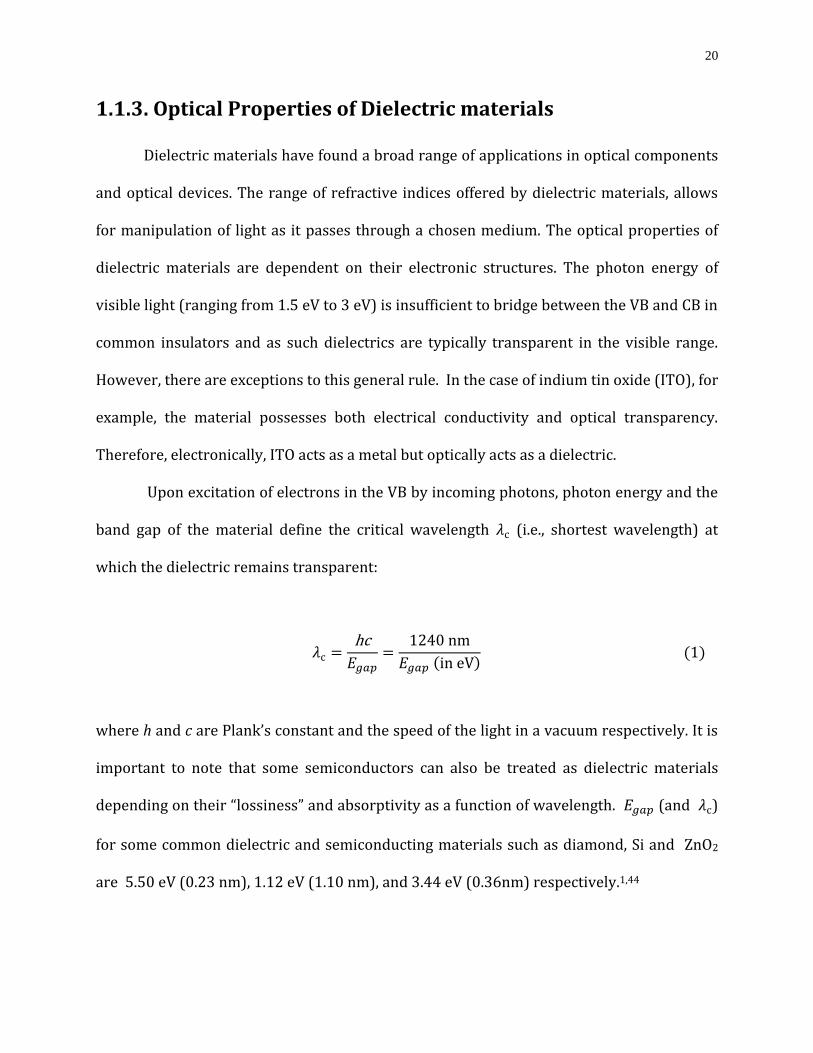
20
1.1.3. Optical Properties of Dielectric materials
Dielectric materials have found a broad range of applications in optical components
and optical devices. The range of refractive indices offered by dielectric materials, allows
for manipulation of light as it passes through a chosen medium. The optical properties of
dielectric materials are dependent on their electronic structures. The photon energy of
visible light (ranging from 1.5 eV to 3 eV) is insufficient to bridge between the VB and CB in
common insulators and as such dielectrics are typically transparent in the visible range.
However, there are exceptions to this general rule. In the case of indium tin oxide (ITO), for
example, the material possesses both electrical conductivity and optical transparency.
Therefore, electronically, ITO acts as a metal but optically acts as a dielectric.
Upon excitation of electrons in the VB by incoming photons, photon energy and the
band gap of the material define the critical wavelength (i.e., shortest wavelength) at
which the dielectric remains transparent:
( ) ( )
where h and c are Plank’s constant and the speed of the light in a vacuum respectively. It is
important to note that some semiconductors can also be treated as dielectric materials
depending on their “lossiness” and absorptivity as a function of wavelength. (and )
for some common dielectric and semiconducting materials such as diamond, Si and ZnO2
are 5.50 eV (0.23 nm), 1.12 eV (1.10 nm), and 3.44 eV (0.36nm) respectively.1,44

21
Unlike metals, the charges in a dielectric (insulator) are bound charges, and thus are
not free to move under the influence of an externally applied field. Although their atoms
and molecules are macroscopically neutral, when subjected to an external electric field,
these charges slightly shift their centroids giving rise to local electric dipoles45 as shown in
Figure1.12.
Figure 1.12. Electric polarization in dielectrics showing ionic (or molecular) and electronic
polarization.45
The dipole moment for one such induced dipole p is given as:
(2)
where Q is the magnitude of the electric charge and d is the distance between the positive
and negative charges. To account for all the dipole moments, these individual dipoles are

22
summed over a microscopically large volume V (as compared to the charges) but
macroscopically small (as compared to the incident wavelength), the result is the
polarization vector P:
∑ ( )
The electric field density D can then be found as:
(4)
where is the dielectric constant of free space, = 8.85×10⁻¹² F/m. Induced electric
dipoles alter the applied field and cause the local field to differ from the applied field. It
should be noted that there is a large number of these induced dipoles per unit volume and
each of these dipoles will effectively influence its neighboring dipoles, therefore the
neighboring dipole is subjected to a different applied field. This problem was solved by
Lorentz by considering that the molecular dimensions are much smaller than the
wavelength of the incident light. Lorentz argued that in the case of a non-polar dielectric
material, the applied field must be replaced by a field which is now known as the Lorentz
field EL given as:46,47
( )
When the applied field Ea is replaced by EL in the harmonic oscillator model of the atom, a
reduction in the resonant frequency is observed, thus dielectric materials have their
resonance in the infrared region of the spectrum while in the visible region of the spectrum
the permittivity is almost constant. For example, in the visible region as discussed in
Chapter 7, dispersion of a metamaterial originates from a metallic component whereas the

23
dielectric component remains transparent, that is, considered to be constant which is an
important factor when designing optical metamaterials. Otherwise, as a consequence of
electron and photon resonances, significant losses may occur adversely affecting the
performance of the metamaterial.
1.2. Self-assembly of Nano-materials
Self-assembly of nanoparticles (NPs) offers a simple, cost-efficient method for
producing ensembles of NPs, as well as the ability to fabricate nanostructures on non-
planar substrates. Assembly of NPs into hierarchical structures to exploit their collective
properties (e.g., electronic, optical, mechanical) have entered into a mature stage in the
field of nanochemistry. This section provides a concise overview of the self-assembly of
NPs and examines the various interparticle forces used in their assembly.
Assembly of NPs can be achieved for example, by exploitation of various forces such
as electrostatic attraction, hydrogen bonding, covalent bonding and dipole-dipole
interactions.48 Specifically tailored interparticle interactions caused by these forces have
resulted in a variety of hierarchical structures (Figure 1.13). For example, by modifying the
surface of the NPs with photoisomerizable molecules, assembly and disassembly of NPs can
be realized via molecular dipole-dipole interactions48 and nanorods can be assembled into
chains via hydrogen bonding of DNA linkers.49
Molecular dipole-dipole interactions are relatively weak. The typical value of
molecules with a permanent electric dipole moment is 0-4 Debye. However, when several
molecules are tethered to the surface of NPs, these molecular dipole interactions can

24
become strong enough to induce NP self-assembly. The total interaction energy Udd due to
molecular dipoles is approximately:48
Udd ≈ uddNdd (3)
where udd is the thermally averaged interactions between freely rotating dipoles and Ndd is
the number of interacting dipole–dipole pairs between the two particles at contact
( dd Aeff where Aeff is an effective area of contact between two spherical NPs with
radius a (≈2 σ ) and is particle s surface density). For example, in the case of 3 nm
Au NPs functionalized with cis-azobenze terminated alkane thiols,50 Ndd may have a value
as large as ~40 with a resultant total interaction energy of approximately 40 kT. Thus,
when acting together, these molecular dipole interactions have sufficient influence to
induce self-assembly.
Figure 1.13. Schematic of the self-assembly of nanoparticles into a variety of hierarchical
structures: chains, bi-layer, ring, and hexagonal arrays.

25
Another example is a magnetic dipole-dipole interaction induced by using spherical
magnetic NPs. This type of assembly exploits the directionality of the dipolar interactions
between particles. This dipolar interaction of NPs is dependent on both the conformation
and size of NPs. The attraction is the strongest when NPs are aligned in an “in-line”
configuration and assembly into chains and rings can be achieved.51-54 For example,
polyisobutene-coated iron NPs with a diameter of 12 nm can form into a “string”
conformation and the magnitude of the interaction is approximately 15kT (i.e.,
). It should be noted that these
assemblies were formed at a relatively low concentration of NPs. At higher concentrations,
the major driving force of the assembly is due to entropic effects rather than magnetic
dipolar–dipolar interactions. In addition, higher dipolar interactions can be realized in the
presence of an applied field shown in Figure 1.14.51,55
Figure 1.14. TEM images of (A) Self-assembly of magnetic dipole–dipole interactions by using 20
nm cobalt nanoparticles in the absence of an external magnetic field. Reprinted with permission
from Reference 51. Copyright 1966, American Institute of Physics. (B) Formation of “ring”
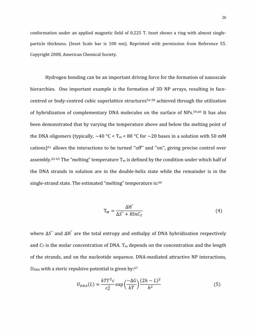
26
conformation under an applied magnetic field of 0.225 T. Inset shows a ring with almost single-
particle thickness. (Inset Scale bar is 100 nm). Reprinted with permission from Reference 55.
Copyright 2008, American Chemical Society.
Hydrogen bonding can be an important driving force for the formation of nanoscale
hierarchies. One important example is the formation of 3D NP arrays, resulting in face-
centred or body-centred cubic superlattice structures56-58 achieved through the utilization
of hybridization of complementary DNA molecules on the surface of NPs.59,60 It has also
been demonstrated that by varying the temperature above and below the melting point of
the DNA oligomers (typically, ~40 °C < Tm < 80 °C for ~20 bases in a solution with 50 mM
cations)61 allows the interactions to be turned ‘‘off’’ and ‘‘on’’, giving precise control over
assembly.62-65 The “melting” temperature Tm is defined by the condition under which half of
the DNA strands in solution are in the double-helix state while the remainder is in the
single-strand state. The estimated “melting” temperature is:66
( )
where and H are the total entropy and enthalpy of DNA hybridization respectively
and CT is the molar concentration of DNA. Tm depends on the concentration and the length
of the strands, and on the nucleotide sequence. DNA-mediated attractive NP interactions,
UDNA with a steric repulsive potential is given by:67
( )
(
)( )
( )

27
where , c, L, and h are surface density of DNA ligands, concentration , separation distance
between NPs and “height” of the grafted DNA respectively. Equation (5) is valid and
qualitatively in good agreement with experiment when h < L < 2h. These highly specific
DNA-mediated interactions are desirable for the self-assembly of nanoscale components
and represent an important example of the role of hydrogen bonding in mediating the
formation of nanostructures.
Electrostatic interactions between NPs are useful for both ensuring colloidal
stability in solution and guiding their self-assembly into hierarchical structures such as
mono- and multi-layer arrays and binary superstructures.68-71 Electrostatic attractions can
either be repulsive or attractive between like-surface charges of NPs or opposite charges
respectively and can also be directional with regard to NPs whose surface charge
distribution is asymmetric. Also, electrostatic attraction can be tuned by the dielectric
constant of the chosen solvent and concentration of surrounding counter ions.
One of the most ubiquitous NP interactions is through van der Waals (vdW) forces
which arise from electromagnetic fluctuations due to the continuous movements of
positive and negative charges between material bodies. vdW forces can be divided into
three groups: (1) thermally averaged dipole-dipole interactions, (2) dipole-induced dipole
interactions and (3) London dispersion interactions between transient dipoles of
polarizable bodies. The attractive vdW force between the atoms is proportional to 1/r7,
where r is the distance between the atoms. The point interactions describing the empirical
potential (Lennard-Jones potential) is given by:72
( )
[(
)
(
)
] ( )

28
where A and C are attractive interaction and repulsive component respectively,
represents the characteristic energy of the interaction between the bodies and is the
collision diameter. In the case of macroscopic bodies, vdW forces are significant at a
distance of a few nm to tens of nms. The interaction between different geometries, such as
two spheres, a sphere and surface, or two crossed cylinders, can be calculated by
integration. Table 1.1 shows vdW interaction free energies between bodies of different
geometries that were calculated based on the Hamaker Summation Method.72
Table 1.1. Van der Waals interaction energy and force between macroscopic bodies of different
geometries with surfaces a distance of D apart where D<<R. R is the radius and A is the Hamaker
constant.72
Geometry of Bodies Van der Waals Interactions Energy Force
Sphere near flat surface E =AR/6D F =AR/6D2 Two identical spheres E = AR/12D F =AR/12D2
Cylinder near flat surface
√
√
√
√
Two identical parallel cylinders
√
√
Two identical cylinders 90° to each other
E =AR/6D F =AR/6D2
The assembly of NPs via vdW forces is predominately limited to surface interactions.
However, there may be additional ‘‘body’’ forces which occur between materials that
possess permanent magnetic or electric polarization. These forces are usually weak and
may be screened in electrolyte solutions. Figure 1.15 shows an example of preferred
orientation of nanorods and spherical NPs as a function of screening length.48 Whereby the
screening length is determined by the electrostatic potential:47,73

29
(
) ( )
where
and kT/e ≈ 25 mV at room temperature describes the electrostatic
potential in the presence of dissolved ions. Therefore, is defined as:73
(
)
( )
where cs is the salt concentration. represents the length scale that approximates the
exponential decay of electrostatic potential when moving away from charged bodies in
solution (e.g., ).
Figure 1.15. (A) Schematic illustration of a charged gold NP interacting with a gold nanorod via
electrostatic interactions. (B) Ratio of the interaction energies for the end and side configurations
as a function of screening length. Reprinted with permission from Reference 48. Copyright 2009,
Small.

30
One of two possible arrangements, “side” or “end” is preferred based on the range of the
electrostatic interactions. When is significantly smaller than the dimensions of the NP,
a spherical, charged NP will interact in preference with the “sides” of an oppositely charged
nanorod, rather than with either of its “ends”. The electrostatic interaction between a
nanorod (radius ar, length h) and a sphere (radius as) scales as Uside ~ asar1/2/(as+ar)1/2 for
the “side” configuration and Uend ~ asar/(as+ar) for the “end” configuration. Therefore, the
“side” arrangement is preferred. It should be noted that vdW forces are only effective from
a distance of a few nm to tens of nms. At a large separation, retardation effects occur due to
the finite speed of light. This retardation effect causes the force to fall more rapidly with
distance than in the short-range vdW limit 1/r6 (~1/r7). It is worth mentioning that casimir
forces can arise from the confinement of the zero point energy fluctuations of the
electromagnetic field between two bodies.74,75 This casimir effect can be present as a
force76-79 in binary liquids where liquid fluctuations confined between two surfaces change
the equilibrium thickness of wetting layers. Also, it can be present as a force between
colloidal particles due to confinement of solvent between the particles leading to
aggregation.
Assembly of NPs at interfaces, e.g., liquid-liquid or liquid-solid, can be achieved via
the adsorption of NPs to a particular interface,80,81 Langmuir-Blodgett deposition
technique,82-84 and sedimentation and evaporation methods.85-87 For example, adsorption
of CdSe NPs at oil-water interfaces is controlled by reduction in the total free energy of the
system. Figure 1.16 shows a confocal microscope image of a water droplet, whose surface
is decorated with tri-n-octylphosphine oxide capped CdSe NPs.80,88 Surface energy
reduction E due to the assembly of a single particle at the oil-water interface is:

31
( ( ))
( )
where are three contributions to the interfacial tensions at the oil-water,
particle-water, and particle-oil interfaces respectively and r is the effective radius of a NP.
An estimate of is approximately -5 kT for 2.8 nm NPs. The competition between
interfacial energy and thermal fluctuations results in size-dependent NP self-assembly, due
to the fact that depends on r2. Therefore, when the NP is smaller (diameter 2.8 nm), the
energy gain is relatively smaller as compared to the larger NPs (diameter 4.6 nm) and as
such the larger NPs replace the smaller NPs.88
In general, nanoscale assembly relies on the premise that careful design of
components e.g., size, geometry, composition and their interactions will allow for the
creation of desired 2D and 3D hierarchical structures. However, in practice, this is a
challenging task and often there is more than one major driving force involved in the
assembly. For example, assembly of 2-(dimethylamino)ethanethiol capped CdTe NPs into
2D sheets is in practice realized by balancing the dipole moment, surface charge and
directional hydrophobic attractions.89
Whether we are considering metals, semiconductors or dielectrics, an
understanding of their optical and electronic properties both individually and collectively,
is a critical first step in the design and formation of functional nanoscale ensembles. From
CdSe semiconductor QD lamellae (Chapter 6), to chains and stacks of gold nanorods
(Chapter 3 and 4 respectively), the common theme is the bottom-up creation of
architectures whose compositional and geometrical design affords the possibility of new
insights and potential applications on the nanoscale.

32
Figure 1.16. Fluorescence confocal microscope images of varying sizes of water droplets in toluene
in which CdSe NPs show self-assembly at the liquid-liquid interface. Optical cross-sectional images
at various depths are shown on the left. Reprinted with permission from Reference 81. Copyright
2003, Science.
1.3. Overview of Metamaterials
Metamaterials are artificially structured composites tailored for their specific
ensemble electromagnetic (EM) properties that are not found in naturally occurring media
and are not observed in the constituent materials components.90-94 The term
“metamaterial” is derived from the Greek word, in which “meta” means “beyond”. Thus
metamaterials are materials having properties ‘beyond’ those of conventional materials.
The heterogeneity of these materials exists on a length scale less than the wavelength of
interest. Thus, the EM response of the material is a function of the collective behavior of the

33
materials components. Figure 1.17 shows a schematic illustration of both a conventional
material and metamaterial.95 In a conventional material, the response to an EM field is
determined by the atoms and molecules, whereas in a metamaterial, the response is
engineered through many identical structural units whose dimensions are less than the
wavelength of the operating frequency.
One subgroup of metamaterials that have received considerable attention, are
referred to as negative refractive index materials.92,96,97 These complex materials possess
negative real values for both permeability and permittivity at certain frequencies.98-100
These materials have their conceptual beginnings with Sir Arthur Schuster who, in 1904
stated “Energy can be carried forward at the group velocity but in a direction that is anti-
parallel to the phase velocity.” and “… the deviation of the wave entering such a medium is
greater than the angle of incidence.”101 In 1967, Veselago theoretically investigated plane-
wave propagation in a material whose permeability and permittivity were assumed to be
simultaneously negative.102 For a monochromatic uniform plane wave in such a medium,
the direction of the Poynting vector is anti-parallel to the direction of the phase velocity. In
recent years, Smith and Schultz et al constructed such a composite medium for the
microwave region and demonstrated experimentally the presence of unusual
refraction.100,103

34
Figure1.17. (A) Naturally occurring conventional material with its atoms (B) Metamaterial
artificially structured “atoms” Figure is adapted from reference 87.
More generally, it is well known that the response of a system to the presence of an
EM field is determined, to a large extent, by the properties of the materials involved. We
describe these properties by defining the macroscopic parameters of their permeability
and permittivity. Figure 1.18 shows permeability and permittivity diagrams for the
classification of a medium separated into four quadrants.
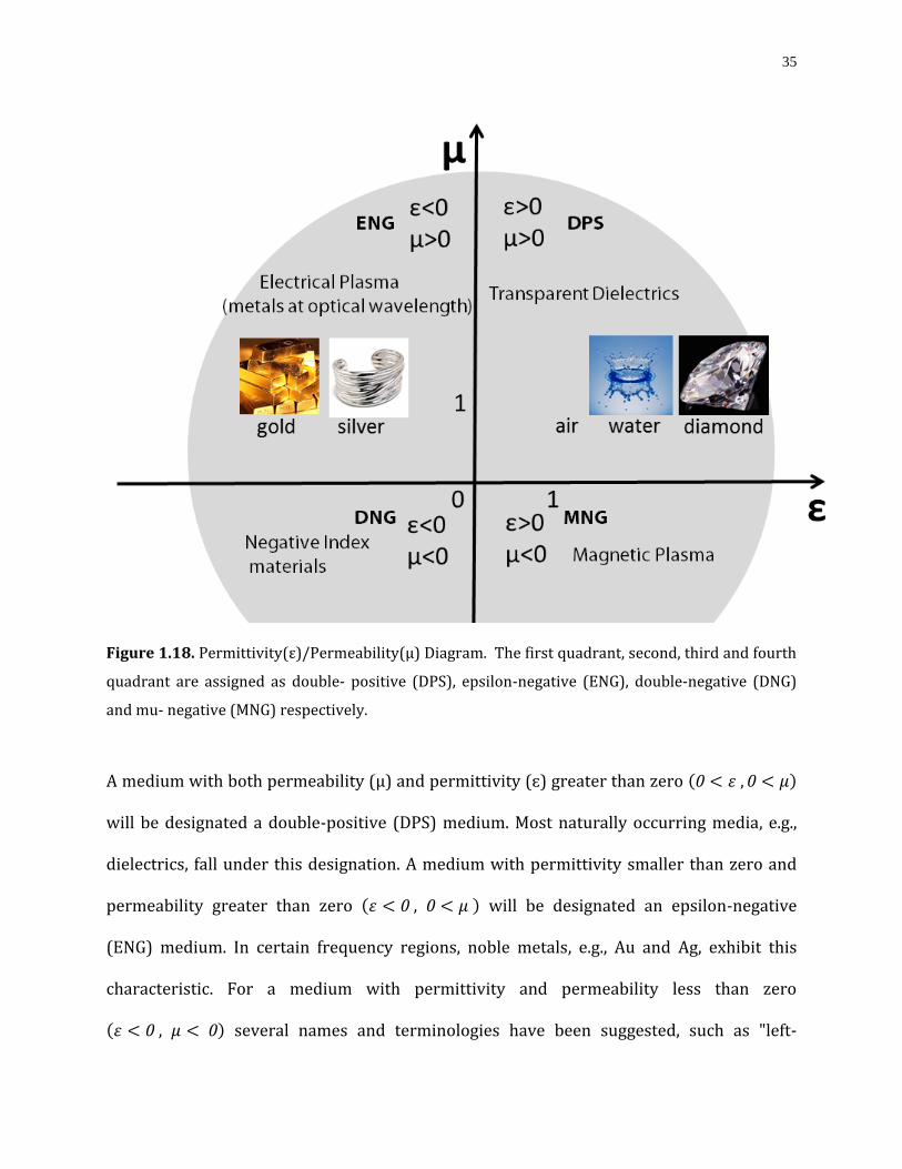
35
Figure 1.18. Permittivity(ε)/Permeability(µ) Diagram. The first quadrant, second, third and fourth
quadrant are assigned as double- positive (DPS), epsilon-negative (ENG), double-negative (DNG)
and mu- negative (MNG) respectively.
A medium with both permeability (µ) and permittivity (ɛ) greater than zero ( )
will be designated a double-positive (DPS) medium. Most naturally occurring media, e.g.,
dielectrics, fall under this designation. A medium with permittivity smaller than zero and
permeability greater than zero ( ) will be designated an epsilon-negative
(ENG) medium. In certain frequency regions, noble metals, e.g., Au and Ag, exhibit this
characteristic. For a medium with permittivity and permeability less than zero
( ) several names and terminologies have been suggested, such as "left-

36
handed" media; media with a negative refractive index; "backward-wave media" (BW
media); and "double-negative” (DNG) materials.104,105 A medium with permittivity greater
than zero and permeability less than zero ( ) will be designated a mu-negative
(MNG) medium.
It is important to note that at optical wavelengths, all naturally occurring media
show no magnetic response and as such, light interacts with the material via its electric
field only. Therefore, µ is always taken to be unity in the visible region. In the past few
years, a number of researchers have proposed methods for the fabrication of
metamaterials. The manipulation and combination of material falling within these
quadrants (Figure 1.18), allows for the fabrication of a variety of metamaterials with
applications ranging from DNG materials to cloaking (Chapter 7).96,106-112
Regarding DNG materials, one possible metamaterial design is shown in Figure
1.19.113 The building block is a pair of nanorods. The unit cell, that is, the metamaterial
“atom”, should be very small relative to the wavelength of interest. The unit cell of the
metamaterial is designed in such a way that an electric field is parallel to the long axis of
the nanorod as shown in Figure 1.19, inducing parallel currents in the paired nanorods.
The magnetic field of the EM wave (perpendicular to the long axis of the nanorods) causes
anti-parallel currents in the nanorods. The path of current flow is completed by the
displacement current at the edges of the nanorods. Thus the structure showed in Figure
1.19 forms an LC resonant circuit, thereby enabling the metamaterial to interact with the
magnetic component of light. This enables the control of light in an unconventional way
such that this anti-parallel current causes the magnetic response of the system.113

37
Figure 1.19. Schematic illustration of the proposed structure for making a double-negative (DNG)
material showing arrays of paired nanorods. The arrows show the direction of current flow. Figure
is adapted from reference 106.
Advances in the fabrication of structures with small (smaller than the wavelength of
visible light) dimensions, have paved the way for creating metamaterials with potential
applications such as new types of beam steerers, modulators, band-pass filters, lenses,
microwave couplers, and antenna radomes.114 One of the interesting features of DNG media
is their ability to provide phase compensation or phase conjugation due to their negative
refraction. This feature can lead to interesting applications in device and component
designs including sub-wavelength cavities, phase-compensated, time-delayed, wave
guiding systems and waveguides with lateral dimensions below diffraction limits.98,114
Another interesting potential application that results from negative-refraction
properties, is sub-wavelength focusing,98 which offers the possibility of a "perfect lens" or
focusing beyond the diffraction limit. This was first recognized by Veselago115 and the
properties of such a slab were first analyzed by Pendry who showed that a slab with a

38
refractive index n 1 in vacuum results in the imaging of objects with sub-wavelength
focus.98 In his analysis of the image formation process in a slab of lossless DNG material, the
evanescent spatial Fourier components can be ideally reconstructed, in addition to the
reconstruction of all of the propagating spatial Fourier components. The evanescent wave
reconstruction is due to the presence of the "growing exponential effect" in the DNG slab.
This effect, in theory, leads to the formation of an image with a resolution higher than the
conventional limit.98 Waves scattered by an object have all the Fourier components:
√
( )
The propagating waves are limited to:
√
(2)
where kt is the transverse wave vector. To resolve features of size ∆ we need a wavelength
smaller than ∆, that is,
(3)
From Equation (1), if the required is greater then (the free space wave number), the
waves become evanescent and therefore these features cannot be resolved. The DNG
material provides a possible solution, if the optical losses are overcome. The evanescent
waves are “re-grown” in a DNG slab and are fully recovered at the image plane. Figure 1.20
summarizes this effect. A detailed discussion of this effect can be found in the field of
Fourier Optics.

39
Figure 1.20. The idea of a perfect lens with sub-wavelength resolution (A) A conventional lens only
collecting the propagating waves: kt < k0 (B) The loss of the evanescent waves in a conventional
imaging system (solid line represents propagating modes whereas dashed lines represents
evanescent modes) (C) The focusing ability of a DNG slab (D) The growth of evanescent waves in
the DNG slab and the restoration of both the propagating and evanescent waves. Figure was
adapted from Reference 91.
Beyond the potential of DNG materials, the manipulation of ε from 0 to 1, while
keeping µ = 1 (DPS quadrant Figure 1.18) offers the possibility of optical cloaking by the
careful combination of metal and dielectric components on the nanoscale. Chapter 7
discusses in detail, one particular bottom-up route for the achievement of this goal.72

40
References
(1) Kittel, C. Introduction to solid state physics; Wiley: New York, 2004.
(2) Maier, S. A. Plasmonics: Fundamentals and applications; 1st ed.; Springer: New York.
(3) Novotny, L.; Hecht, B. Principles of Nano-Optics; 1st ed.; Cambridge University Press:
New York, 2006.
(4) Ritchie, R. H. Phys Rev 1957, 106, 874.
(5) Raether, H. Surface plasmons; Springer: Berlin, 1988.
(6) Cottam, M. G. Introduction to surface and superlattice exciations; Cambridge University
Press: New York, 1989.
(7) Barnes, W. L.; Dereux, A.; Ebbesen, T. W. Nature 2003, 424, 824.
(8) Willets, K. A.; Van Duyne, R. P. Annu Rev Phys Chem 2007, 58, 267.
(9) Satoshi, K.; Motoichi, O.; Masahiro, I.; Springer: Verlag Berlin Heidelberg New York,
2002.
(10) Homola, J. Surface plasmon resonance based sensors; Springer: Verlag Berlin
Heidelberg, 2006.
(11) Fendler, J. H.; Hutter, E. Adv Mater 2004, 16, 1685.
(12) Willets, K. A.; Van Duyne, R. P. In Annu Rev Phys Chem 2007; Vol. 58, p 267.
(13) Jackson, J. D. Classical Electrodynamics; 3rd ed.; John Wiely&Sons: New York, 1999.
(14) Schatz, G. C.; Kelly, K. L.; Coronado, E.; Zhao, L. L. J Phys Chem B 2003, 107, 668.
(15) Bohren, C. F.; D.R., h. Absorption and scattering of light by small particles; 1st ed.; John
Wiley & Sons: New York, 1983.
(16) Mie, G. Ann Phys-Berlin 1908, 25, 377.

41
(17) Kreibig, U.; Vollmer, M. Optical properties of metal clusters; Springer: Berlin, 1995.
(18) Zhang, X.; Su, K. H.; Wei, Q. H.; Mock, J. J.; Smith, D. R.; Schultz, S. Nano Lett 2003,
3, 1087.
(19) Nurmikko, A. V.; Atay, T.; Song, J. H. Nano Lett 2004, 4, 1627.
(20) Nordlander, P.; Oubre, C.; Prodan, E.; Li, K.; Stockman, M. I. Nano Lett 2004, 4, 899.
(21) Jain, P. K.; Huang, W.; El-Sayed, M. A. Nano Lett 2007, 7, 2080.
(22) Jain, P. K.; El-Sayed, M. A. J Phys Chem C 2008, 112, 4954.
(23) Gluodenis, M.; Foss, C. A. J Phys Chem B 2002, 106, 9484.
(24) Funston, A. M.; Novo, C.; Davis, T. J.; Mulvaney, P. Nano Lett 2009, 9, 1651.
(25) Fromm, D. P.; Sundaramurthy, A.; Schuck, P. J.; Kino, G.; Moerner, W. E. Nano Lett
2004, 4, 957.
(26) Muskens, O. L.; Giannini, V.; Sanchez-Gil, J. A.; Rivas, J. G. Opt Express 2007, 15,
17736.
(27) Jain, P. K.; Eustis, S.; El-Sayed, M. A. J Phys Chem B 2006, 110, 18243.
(28) Hicks, E. M.; Zou, S. L.; Schatz, G. C.; Spears, K. G.; Van Duyne, R. P.; Gunnarsson, L.;
Rindzevicius, T.; Kasemo, B.; Kall, M. Nano Lett 2005, 5, 1065.
(29) Felidj, N.; Aubard, J.; Levi, G.; Krenn, J. R.; Schider, G.; Leitner, A.; Aussenegg, F. R.
Phys Rev B 2002, 66.
(30) Zhao, L. L.; Kelly, K. L.; Schatz, G. C. J Phys Chem B 2003, 107, 7343.
(31) Haynes, C. L.; McFarland, A. D.; Zhao, L. L.; Van Duyne, R. P.; Schatz, G. C.;
Gunnarsson, L.; Prikulis, J.; Kasemo, B.; Kall, M. J Phys Chem B 2003, 107, 7337.
(32) Auguie, B.; Barnes, W. L. Phys Rev Lett 2008, 101.

42
(33) Krenn, J. R.; Dereux, A.; Weeber, J. C.; Bourillot, E.; Lacroute, Y.; Goudonnet, J. P.;
Schider, G.; Gotschy, W.; Leitner, A.; Aussenegg, F. R.; Girard, C. Phys Rev Lett 1999, 82,
2590.
(34) Maier, S. A.; Brongersma, M. L.; Kik, P. G.; Atwater, H. A. Physical Review B 2002, 65.
(35) Lamprecht, B.; Schider, G.; Lechner, R. T.; Ditlbacher, H.; Krenn, J. R.; Leitner, A.;
Aussenegg, F. R. Phys Rev Lett 2000, 84, 4721.
(36) Klimov, V. I. Annu Rev Phys Chem 2007, 58, 635.
(37) Nie, S. M.; Smith, A. M. Accounts Chem Res 2010, 43, 190.
(38) Efros, A. L.; Rosen, M. Annual Review of Materials Science 2000, 30, 475.
(39) Efros, A. L.; Rosen, M.; Kuno, M.; Nirmal, M.; Norris, D. J.; Bawendi, M. Phys Rev B
1996, 54, 4843.
(40) Crooker, S. A.; Barrick, T.; Hollingsworth, J. A.; Klimov, V. I. Appl Phys Lett 2003, 82,
2793.
(41) Ekimov, A. I.; Hache, F.; Schanneklein, M. C.; Ricard, D.; Flytzanis, C.; Kudryavtsev, I.
A.; Yazeva, T. V.; Rodina, A. V.; Efros, A. L. J Opt Soc Am B 1993, 10, 100.
(42) Norris, D. J.; Sacra, A.; Murray, C. B.; Bawendi, M. G. Phys Rev Lett 1994, 72, 2612.
(43) Nirmal, M.; Norris, D. J.; Kuno, M.; Bawendi, M. G.; Efros, A. L.; Rosen, M. Phys Rev
Lett 1995, 75, 3728.
(44) Palik, E. D. Handbook of optical constants of solids; Academic Press: New York, 1997.
(45) Balanis, C. A. Advanced engineering constants of solids; Wiley: New York, 1989.
(46) Born, M.; Wolf, E. Principles of Optics: Electromagnetic Theory of Propagation,
Interference and Diffraction of Light Cambridge University Press: Cambridge, 2002.
(47) Parson, W. W. Modern Optical Spectroscopy; Springer: Verlag Berlin Heidelberg, 2007.

43
(48) Grzybowski, B. A.; Bishop, K. J. M.; Wilmer, C. E.; Soh, S. Small 2009, 5, 1600.
(49) Thomas, K. G.; Barazzouk, S.; Ipe, B. I.; Joseph, S. T. S.; Kamat, P. V. J Phys Chem B
2004, 108, 13066.
(50) Leff, D. V.; Ohara, P. C.; Heath, J. R.; Gelbart, W. M. J Phys Chem-Us 1995, 99, 7036.
(51) Thomas, J. R. J Appl Phys 1966, 37, 2914.
(52) Tanase, M.; Bauer, L. A.; Hultgren, A.; Silevitch, D. M.; Sun, L.; Reich, D. H.; Searson,
P. C.; Meyer, G. J. Nano Lett 2001, 1, 155.
(53) Chen, Q. W.; Niu, H. L.; Zhu, H. F.; Lin, Y. S.; Zhang, X. J Mater Chem 2003, 13, 1803.
(54) Tanase, M.; Silevitch, D. M.; Hultgren, A.; Bauer, L. A.; Searson, P. C.; Meyer, G. J.;
Reich, D. H. J Appl Phys 2002, 91, 8549.
(55) Tripp, S. L.; Pusztay, S. V.; Ribbe, A. E.; Wei, A. J Am Chem Soc 2002, 124, 7914.
(56) Gang, O.; Nykypanchuk, D.; Maye, M. M.; van der Lelie, D. Nature 2008, 451, 549.
(57) Park, S. Y.; Obayashi, E.; Yoshida, H.; Kawai, F.; Shibayama, N.; Kawaguchi, A.;
Nagata, K.; Tame, J. R. H. Nature 2008, 454, 1127.
(58) Sun, D.; Gang, O. J Am Chem Soc 2011, 133, 5252.
(59) Mirkin, C. A.; Letsinger, R. L.; Mucic, R. C.; Storhoff, J. J. Nature 1996, 382, 607.
(60) Alivisatos, A. P.; Johnsson, K. P.; Peng, X. G.; Wilson, T. E.; Loweth, C. J.; Bruchez, M.
P.; Schultz, P. G. Nature 1996, 382, 609.
(61) Rychlik, W.; Rhoads, R. E. Nucleic Acids Res 1989, 17, 8543.
(62) Rotello, V. M.; Boal, A. K.; Ilhan, F.; DeRouchey, J. E.; Thurn-Albrecht, T.; Russell, T.
P. Nature 2000, 404, 746.
(63) Wang, J. F.; Sun, Z. H.; Ni, W. H.; Yang, Z.; Kou, X. S.; Li, L. Small 2008, 4, 1287.

44
(64) Huskens, J.; Mulder, A.; Auletta, T.; Nijhuis, C. A.; Ludden, M. J. W.; Reinhoudt, D. N.
J Am Chem Soc 2004, 126, 6784.
(65) Turnbull, W. B.; Badjic, J. D.; Nelson, A.; Cantrill, S. J.; Stoddart, J. F. Accounts Chem
Res 2005, 38, 723.
(66) SantaLucia, J. P Natl Acad Sci USA 1998, 95, 1460.
(67) Biancaniello, P. L.; Kim, A. J.; Crocker, J. C. Phys Rev Lett 2005, 94.
(68) Grzybowski, B. A.; Smoukov, S. K.; Bishop, K. J. M.; Kowalczyk, B.; Kalsin, A. M. J
Am Chem Soc 2007, 129, 15623.
(69) Yang, B.; Hao, E. C.; Zhang, J. H.; Zhang, X.; Sun, J. Q.; Shen, S. C. J Mater Chem
1998, 8, 1327.
(70) Rubner, M. F.; Lee, D.; Cohen, R. E. Nano Lett 2006, 6, 2305.
(71) Willner, I.; Shipway, A. N.; Lahav, M.; Gabai, R. Langmuir 2000, 16, 8789.
(72) J.N., I. Intermolecular and Surface Forces; 3rd ed.; Academic Press, 2011.
(73) Israelachvili, J. Intermolecular and surface forces; Academic Press: New York, 1985.
(74) Casimir, H. B. G. Proc. K. Ned. Akad. Wet 1948, 60, 793.
(75) Milonni, P. W. The Quantum Vacuum: An Introduction to Quantum Electrodynamics;
Academic: San Diego, 1993.
(76) M. Fukuto, Y. F. Y., P. S. Pershan, Phys. Rev. Lett. 2005, 94, 135702
(77) S. Rafai, D. B., J. Meunier, Physica (Amsterdam) 2007, 386A, 31.
(78) Hertlein, C.; Helden, L.; Gambassi, A.; Dietrich, S.; Bechinger, C. Nature 2008, 451,
172.
(79) Soyka, F.; Zvyagolskaya, O.; Hertlein, C.; Helden, L.; Bechinger, C. Phys. Rev. Lett.
2008, 101.

45
(80) Boker, A.; He, J.; Emrick, T.; Russell, T. P. Soft Matter 2007, 3, 1231.
(81) Kinge, S.; Crego-Calama, M.; Reinhoudt, D. N. Chemphyschem 2008, 9, 20.
(82) Yang, P. D.; Tao, A. R.; Huang, J. X. Accounts Chem Res 2008, 41, 1662.
(83) Collier, C. P.; Saykally, R. J.; Shiang, J. J.; Henrichs, S. E.; Heath, J. R. Science 1997,
277, 1978.
(84) Yang, P.; Tao, A.; Sinsermsuksakul, P. Nat Nanotechnol 2007, 2, 435.
(85) Talapin, D. V.; Shevchenko, E. V.; Kotov, N. A.; O'Brien, S.; Murray, C. B. Nature
2006, 439, 55.
(86) Courty, A.; Courty, A.; Mermet, A.; Albouy, P. A.; Duval, E.; Pileni, M. P. Nat Mater
2005, 4, 395.
(87) Cheng, W. L.; Campolongo, M. J.; Cha, J. J.; Tan, S. J.; Umbach, C. C.; Muller, D. A.;
Luo, D. Nat Mater 2009, 8, 519.
(88) Emrick, T.; Lin, Y.; Skaff, H.; Dinsmore, A. D.; Russell, T. P. Science 2003, 299, 226.
(89) Kotov, N. A.; Tang, Z. Y.; Zhang, Z. L.; Wang, Y.; Glotzer, S. C. Science 2006, 314,
274.
(90) Pendry, J. B.; Holden, A. J.; Stewart, W. J.; Youngs, I. Phys Rev Lett 1996, 76, 4773.
(91) Pendry, J. B.; Holden, A. J.; Robbins, D. J.; Stewart, W. J. Ieee T Microw Theory 1999,
47, 2075.
(92) Ziolkowski, R. W. Phys Rev E 2004, 70.
(93) Alu, A.; Engheta, N. Ieee T Microw Theory 2004, 52, 199.
(94) Goussetis, G.; Feresidis, A. P.; Harvey, A. R. J Mod Optic 2010, 57, 1.
(95) Pendry, J. Nat Mater 2006, 5, 599.
(96) Shalaev, V. M. Nature Photonics 2007, 1, 41.

46
(97) Pendry, J. B. Contemp Phys 2004, 45, 191.
(98) Pendry, J. B. Phys Rev Lett 2000, 85, 3966.
(99) Caloz, C.; Itoh, T. Ieee Microw Wirel Co 2003, 13, 547.
(100) Smith, D. R.; Padilla, W. J.; Vier, D. C.; Nemat-Nasser, S. C.; Schultz, S. Phys Rev Lett
2000, 84, 4184.
(101) Schuster, A. An introduction to the theory of optics; London E Arnold 1904.
(102) Veselago, V. G. Fiz Tverd Tela+ 1967, 8, 2854.
(103) Shelby, R. A.; Smith, D. R.; Schultz, S. Science 2001, 292, 77.
(104) Iyer, A. K.; Eleftheriades, G. V. 2002 Ieee Mtt-S International Microwave Symposium
Digest, Vols 1-3 2002, 1067.
(105) Lindell, I. V.; Tretyakov, S. A.; Nikoskinen, K. I.; Ilvonen, S. Microw Opt Techn Let
2001, 31, 129.
(106) Hrabar, S.; Bartolic, J.; Sipus, Z. Ieee Antennas and Propagation Society Symposium,
Vols 1-4 2004, Digest 2004, 2568.
(107) Ziolkowski, R. W.; Kipple, A. D. Phys Rev E 2003, 68.
(108) Klar, T. A.; Kildishev, A. V.; Drachev, V. P.; Shalaev, V. M. Ieee J Sel Top Quant 2006,
12, 1106.
(109) Smith, D. R.; Pendry, J. B.; Wiltshire, M. C. K. Science 2004, 305, 788.
(110) Engheta, N. Science 2007, 317, 1698.
(111) Chen, H.; Wu, B. I.; Kong, J. A. J Electromagnet Wave 2006, 20, 2137.
(112) Chen, H.; Chan, C. T.; Sheng, P. Nat Mater 2010, 9, 387.
(113) Shalaev, V. M.; Cai, W. S.; Chettiar, U. K.; Yuan, H. K.; Sarychev, A. K.; Drachev, V.
P.; Kildishev, A. V. Opt Lett 2005, 30, 3356.

47
(114) Engheta, N. Nato Sci Ser Ii Math 2002, 89, 19.
(115) Veselago, V. G. Sov Phys Uspekhi 1968, 10, 509.
.

48
Chapter 2
Materials and Methods
2.1. Materials
Tri-n-octylphosphine oxide (TOPO, tech. grade 90%) and Tri-n-octylphosphine
(TOP), Cadmium Oxide (CdO, ~99%), Selenium (powder, 99.999%), Steric acid, Cadmium
acetate dihydrate (~98%) were purchased from Sigma-Aldrich and used as received.
Hexadecyltrimethylammoniumbromide (CTAB, 98%) was purchased from Fluka. Sodium
borohydride (99%) and l-ascorbic acid were purchased from Sigma-Aldrich. Thiolated
Polystyrene was purchased from Polymer Science. 25 micrometer diameter Aluminum
wire (99.999%) was purchased from Alpha-Aesar. Perchloric, Oxalic acid, Silver Nitrate,
Sodium Sulfide (anhydrous) and Ethlyene Glycol were purchased from Sigma-Aldrich.
Deionized water (18 MΩ) from a Millipore Milli-Q water purification system was used in all
the experiments.

49
2.2. Methods
2.2.1. Synthesis and Fabrication
2.2.1.1. Synthesis of CdSe Quantum Dots and Nanorods
TOPO capped CdSe quantum dots (QDs) were synthesized through an established
organometallic approach at high temperature.1,2 In a typical CdSe QD synthesis, CdO (63
mg) was dissolved in a mixture of steric acid (1g) and 3g of TOPO by first evacuating at
80 C for 2 h, followed by heating at 340 C under an Ar atmosphere. Once an optically clear
solution was achieved, selenium in tri-n-octylphosphine (Se-TOP; 37 mg in 1.0 mL) was
injected rapidly at 310 C. QDs were then allowed to grow for 1-20 min at 280 C and an
aliquot was taken out to examine the quality of the CdSe QDs. Once CdSe QDs of desired
dimensions were grown, QD growth was terminated by removal of the heating mantle, and
at 50 C, anhydrous methanol (MeOH) was added to the mixture to precipitate the QDs.
Purification was achieved by centrifugation (2×). As synthesized TOPO-capped CdSe QDs
were dissolved in toluene (good solvent) and temporal stability is typically many months.
CdSe nanorods were prepared as described elsewhere3 with the exception that a
mixture of equimolar amounts (9 mmol) of Cd(OAc)2 ·2H2O and NH4(OAc) was used in the
multiinjection step. In a typical synthesis, CdO (0.096 g), TDPA (0.430 g), and TOPO (3.88
g) were loaded into a 25 mL round-bottom flask. The mixture was heated to 320 C under
an argon flow. Once a colorless homogeneous solution was formed, a solution of TOPSe in
TOP (0.51 mL, 1 M) was then injected into the solution. Subsequent multiple injections
were performed over 5 min using an automated syringe pump and samples were taken out

50
at 3 and 6 min. Purification of CdSe bullet-shaped rods was carried out using the procedure
for CdSe QDs as described above.
2.2.1.2. Synthesis of Gold Nanorods
Gold NRs were prepared by the ‘seed-mediated growth method’ devised by El-
Sayed4. Briefly, seed gold NPs were synthesized by the reduction of HAuCl4, dissolved in an
aqueous solution of cetyltrimethylammonium bromide (CTAB), with cold sodium
borohydride (NaBH4). The growth solution was prepared by dropwise addition of ascorbic
acid in an aqueous solution of HAuCl4, CTAB and AgNO3. A seed solution aged for 5 min was
added to the growth solution and the NR growth was initiated. The color of the solution
mixture changed from clear to deep-purple after incubation for 10 hr at 27°C. The resultant
CTAB-coated gold NRs were purified by two centrifugation cycles (8500 rpm for 30 min).
2.2.1.3. Fabrication of Al2O3/Ag hybrid Cloaking Structure
25 micrometer diameter aluminum wire was first degreased in a 1:1 mixture of
acetone and propanol. The wire was then electropolished in a 1:5 mixture of perchloric
acid and propanol. The electropolishing was carried out at a constant potential of 20 V. In
order to produce the desired final diameter of 3 to 4 µm, the wire was repeatedly dipped
and removed from the electropolishing bath to create a tapered profile. The final desired
wire diameter was confirmed by light microscopy. Following electropolishing the wire was
washed in distilled water then rinsed with acetone.

51
Porous Al2O3 growth was carried out using a 3 % oxalic acid solution at 21°C. In
order to produce the desired radial oxide growth with the appropriate gradation in pore
volume, the applied potential was varied from 30 V to 18 V over a period of 100 minutes.
Specifically, voltage was held at 30 V for 20 mins, 24 V for 30 mins and 18 V for 50 mins. At
each voltage transition, a rate of 1V per min was used. The wire was removed from the
oxalic acid solution and washed in distilled water then rinsed with acetone.
Electroless deposition of Ag nanowires was carried out by placing the AAO coated
aluminum wire into ethylene glycol containing 12 % AgNO3 and 30 µmol of Na2S. The
solution containing the wire was first sonicated for 5 min at 42 kHz then placed in an oven
at 155°C for 30 minutes. After removal from the solution, the wire was then paced in a
slurry of propanol and diamond polishing powder and sonicated for 5 minutes at 42 kHz.
This step is necessary to remove superficial Ag crystalline deposits.
2.2.2. Self-assembly of Semiconductor and Metal Nanoparticles
2.2.2.1. Assembly of Quantum Dot Lamellar Envelopes
Trioctylphosphine oxide (TOPO) capped CdSe quantum dots (QDs) and nanorods
were synthesized through an established organometallic approach at high temperature and
described in section 2.2.1.1. As-synthesized TOPO capped CdSe QDs or nanorods were
precipitated with methanol three times to remove free TOPO and then dissolved in toluene.
For optimmized lamellar formation, 10 μL of deionized water (10% v/v) were added into
CdSe QDs (9.84 × 10⁻⁷ mol/L) dissolved in toluene (20% v/v water was used for nanorods).
The mixtures were sonicated from 15 to 30 s at 42 kHz. A cloudy, colored suspension

52
formed immediately following sonication. The sample was withdrawn via micropipette for
further characterization. For all encapsulation experiments, 10 μL (10% v/v) of water-
soluble species (CoCl2 ·6H2O, 6.09 × 10⁻² M; EuCl3 ·6H2O, 7.39 × 10⁻² M; Au NPs ∼37.8
nM, and ferritin 53mg/mL in 0.15 M NaCl) were added as described above for water.
2.2.2.2. Assembly of Gold Nanorods
For end-to-end NR assembly, 760 μL of tetrahydrofuran (THF) were evaporated from
the stock NR solution. The dried NRs were re-dissolved in 2.45 mL of dimethylformamide
(DMF). A solution of Raman reporter molecule of Oxazine 720 (OX) in DMF (4 µM) was
added dropwise under shaking to the NR solution in DMF. Following a 30 min agitation
under gentle vortex conditions, the mixture was incubated for 1 hr. The end-to-end self-
assembly of the NRs was triggered by a dropwise addition of the DMF-water mixture
containing 20 vol. % of water. Side-by-side assembly of gold NRs was similar to that
described above with the exception that Cresyl Violet (CV) was introduced (3 µM) as a
Raman reporter and 10 vol. % of water was introduced into the THF solution containing
NRs.
All subsequent physical measurements were carried out on the same batch of NRs. As
soon as NR self-assembly began, we carried out at regular time intervals, parallel extinction
and SERS measurements, as well as the preparation of samples for electron microscopy
experiments to maximize the fidelity of results.

53
2.2.3. Characterization
2.2.3.1. Electron Microscopy
For the characterization of the structure of lamellar QD Arrays (see chapter 6),
scanning transmission electron microscopy (STEM) was used. A single droplet of solution
(∼25 μL) was applied to 200 or 400 mesh carbon coated copper TEM grids and also to
1000 mesh uncoated TEM grids. Images in both bright field and high angle annular dark
field (HAADF) were recorded using the Hitachi HD-2000 dedicated STEM operating at 200
kV. For the cross-sectional analysis, samples were first prepared on carbon coated indexed
TEM grids. STEM was used to identify the locations of individual lamellae. Subsequently,
the indexed grids were coated with ∼10 nm of carbon using an Emitech high vacuum
carbon coater. Grids were then coated with a 20-30 nm layer of Au using a Denton Desk II
sputter coater. The indexed grids were then embedded in epoxy resin, and 30 nm cross
sections were prepared using a Leica Ultramicrotome (Figure 2.1).

54
Figure 2.1. Cross-sectional sample preparation for internal structure investigation of lamellae by
STEM. (A) CdSe QD and nanorod lamellae were prepared on separate carbon coated indexed TEM
grids. STEM was used to identify the locations of individual lamellae. (B) the indexed grids were
then coated with approx. 10nm of carbon via evaporation to secure the structure. (C) Grids were
then sputtered with a 20-30nm layer of Au which was used as a visual marker in imaging. (D) The
indexed grids were then embedded in epoxy resin and 30nm cross-sections through individual
lamellae were prepared by ultramicrotomy.
For solution state imaging of lamellae, samples (∼15 μL) were injected into
Quantomix WETSEM capsules and backscattered electron images recorded using a Hitachi
S-3400 SEM operating at 20 kV and with the Hitachi TM-1000 table top variable pressure
SEM operating at 15 kV. Energy dispersive X-ray spectroscopy (EDS) in both SEM and
STEM was carried out using an Oxford Instruments INCA system. STEM EDS analysis of
cross sections of QD lamellae was performed at -120 °C to minimize electron beam damage
55
and contamination during X-ray acquisition. Simultaneous TEM and SEM were recorded
using a Hitachi S-5200 field emission SEM equipped with a transmitted electron detector.
Selected area electron diffraction (SAED) patterns of CdSe QDs and nanorods and
their lamellar structures were recorded using an FEI Technai 20 operating at 200 kV.
Subsequent analysis of polycrystalline ring patterns was carried out using the Process
Diffraction software package.5
2.2.3.2. Surface-Enhanced Raman Scattering Spectroscopy
In SERS measurements, 1.5 mL of the solution of self-assembled NRs was placed in a
vial. Raman spectra excited with a 785 nm laser line were acquired with a Renishaw InVia
System spectrometer coupled to a Leica microscope. The laser power was set to 1% of the
full power (approximately 80 µW). The laser beam was focused on the sample by a 5 x
objective lens (NA= 0.12). The calculated interrogated volume was 6.46 nL. The spectra
were measured with a 4 cm-1 resolution, using a 1 sec exposure and 25 scans.
Control SERS experiments were conducted using a roughened gold substrate. A solid
gold electrode with the surface area of 0.3 cm2 was roughened with 20 successive
oxidation-reduction cycles from -0.3 V to +1.25 V at 100 mV/s in an aqueous 0.1 M KCl
working solution. Then, the electrode was isolated from the electrochemical cell and
exposed to a 4 µM solution of OX in water, in pure DMF or in the DMF/water mixture (20
vol. % of water). After 15 min exposure, the surface was rinsed with an appropriate
solvent, that is, with water, DMF or the DMF/water mixture, respectively, and dried under

56
nitrogen flux. The SERS spectra of the OX adsorbed to the gold substrate were acquired
using excitation at 785 nm (laser power 1%, 4 accumulations and 5 s exposure time).
2.2.3.3. Confocal Microscopy
Liquid state confocal fluorescence microscopy of CdSe QD lamellae was carried out
using a Leica TCP SP2 upright confocal microscope with a ×63 1.4 oil immersion lens. The
364 nm line on an Innova 90C Argon ion laser was used for excitation with the signal
collected over a range from 550 to 600 nm. Fluorescence intensity studies were carried out
by recording a series of sequential fluorescence images in the range from 500 to 700 at 5
nm intervals. Again, the 364 nm line of an Innova 90C Argon ion laser was used for
excitation (power: 130 mW ± 1 with 50 % laser power, pinhole: open, zoom 4, gain PMT1:
700V). For the analysis of dye (FITC 100 ng/mL) incorporation into the lamellae,
fluorescent images were obtained using a Leica TCS SP2 confocal microscope with a ×63
1.4 oil immersion lens. Both FITC and QD lamellae were excited using the 488 nm line of an
argon ion laser. FITC emission was collected in the range 490-530 nm Ch1 (green). CdSe
QD emission was collected in the range 550-600 nm Ch2 (yellow).
2.2.3.4. Extinction
The progress of gold NR assemblies for both end-to-end and side-by-side conformations
were monitored by using a Cary 500 UV/vis/near-IR spectrophotometer. Extinction
measurements were recorded in the spectral range from 400-1200 nm at room
temperature.

57
2.2.3.5. Optical Transmission Measurements
To assess the performance of the fabricated cloaking structure, we used the
transmission setup shown in Figure 2.2 which is comprised of a dual optical microscope
(Olympus) coupled to a super-continuum source (Fianium SC-400-4) with a tunable filter.
It allows for high spectral density (>1mW/nm), diffraction limited transmission imaging
from 420 nm to 2000 nm. The output of the laser source is fed to an acousto-optic tunable
filter (AOTF) to choose the desired wavelength from a broad spectrum. Output of AOTF
having a spectral purity of 3nm to 7nm full width half maximum (FWHM) is passed through
a polarizer to ensure TM illumination. A microscope objective (MO) is utilized to focus light
on the sample and collect the scattered radiation. The collected light is fed to a CCD and
spectrometer via a beam splitter (BS) to monitor the field profile and spectral quality of the
laser source.
Figure 2.2. Optical transmission setup using super-continuum (SC) laser source along with an
acousto-optic tunable filter (AOTF) for monochromatic illumination of the cloak sample.

58
2.2.4. Finite-Difference Time-Domain Simulations
The assembly of NR chains was simulated by the 3D finite-difference time-domain
(3D-FDTD) method6. The time and space derivatives were numerically modelled using the
central difference scheme, which is the second order accurate representation of the
analytical Maxwell’s equations. Basics of FDTD are summarized in Appendix A1. Incident
field polarization was parallel to the rod axis and simulation domain was terminated with
perfectly matched layer (PML). The gold NRs were modelled using a fit to Johnson &
Christy’s experimental data.7
To calculate the absorption and scattering cross-sections we employed the formalism
of total field scattered field (TFSF). We introduced a set of 2D power monitors forming two
closed surfaces enclosing the NRs, one inside the TF region (power monitor 1, (PM1)) and
the other in the SF region (power monitor 2, (PM2)). PM1 was used to calculate the
absorption cross-section by evaluating the net power flow into PM1, which represents the
power lost in the NRs. Total power exiting PM2 was used for the calculation of scattering
cross-section as follows where is the scattered power obtained from
PM2 and is the source intensity. The calculated extinction cross-section is the summation
of scattering and absorption cross-sections.

59
References
1. Murray, C. B.; Norris, D. J.; Bawendi, M. G. J. Am. Chem. Soc. 1993, 115, 8706–8715.
2. Peng, Z. A.; Peng, X. G. J. Am. Chem. Soc. 2001, 123, 183–184.
3. Nair, P. S.; Fritz, K. P.; Scholes, G. D. Small 2007, 3, 481–487.
4. Nikoobakht, B.; El-Sayed, M. A. Chem.Mater.2003, 15, 1957-1962.
5. Labar, J. L. Ultramicroscopy 2005, 103, 237–249.
6. Taflove, A.; Hagness, S. C. Computational Electrodynamics: The Finite-Difference Time
Domain Method, 2nd ed.; Artech House: Boston, 2000.
7. Johnson, P. B.; Christy, R. W. Phys. Rev. B 1972, 6, 4370–4379.

60
Chapter 3
Probing Dynamic Generation of Hot-Spots
in Self-Assembled Chains of Gold
Nanorods by Surface Enhanced Raman
Scattering
Elements reprinted with permission from Journal of the American Chemical Society, 133, 7563, 2011. Copyright 2011, American Chemical Society.
Continuing progress in the applications of self-assembled nanostructures depends
critically on establishing a fundamental understanding of the relation between the
properties of nanoparticle ensembles and their time-dependent structural characteristics.
By following the dynamic generation of hot-spots in self-assembled chains of gold
nanorods, we have established a direct correlation between ensemble-averaged surface-
enhanced Raman scattering and extinction properties of these nanoscale chains.
Experimental results were supported by comprehensive finite-difference time-domain
simulations. The relationship established between the structure of nanorod ensembles and
their optical properties provides a basis for producing dynamic, solution-based, plasmonic
platforms for applications ranging from sensing to nanoelectronics.

61
3.1. Introduction
Hierarchical organization of individual nanoparticles (NPs) into complex
nanostructures, including superlattices or small clusters, remains a frontier area of
research in nanoscience. While individual NPs offer a multitude of scientific challenges
and applications, ensembles of NPs show unique, coupled properties which may potentially
be exploited in functional nanoscale devices.1-6 Self-assembly of NPs offers a facile, low cost,
solution-based route for producing ensembles of NPs, along with the ability to fabricate
nanostructures on nonplanar substrates.7-12 To date, self-assembled nanostructures
composed of metal, semiconductor, and magnetic NPs have found applications in the areas
of data storage, imaging, and sensing of chemical and biochemical species.13-21 The
exploitation of self-assembled nanostructures in other applications, is limited in
comparison with those produced by nanofabrication techniques, largely because of the
difficulty in forming defect-free structures with precisely controlled geometry and distance
between adjacent NPs. Additionally, a fundamental understanding of the relationship
between the properties of self-assembled NP clusters and their dynamic structural
characteristics such as aggregation number, mutual NP orientation, and interparticle
distance is required. With this framework of understanding in place, it should be possible
to more accurately and reproducibly predict the properties of self-assembled structures,
both theoretically and practically.
In the case of metal nanocrystals, gold NPs in particular (with various shapes) have
been organized into a variety of nanostructures including chains, two-dimensional sheets,
and superlattices.22-26 When compared to shape isotropic NPs, the self-assembly of
anisotropic gold nanorods (NRs) provides potentially more useful applications, since it

62
offers the ability to exploit vectorial properties of the resultant nanostructures.27-29 The
optical properties of ensembles of gold NRs are typically characterized by measurements of
extinction in the visible and near-infrared spectral ranges. In individual gold NRs, two types
of localized surface plasmon resonances (LSPRs) are observed. These are due to the
coherent oscillations of the conduction band electrons in directions that are parallel and
perpendicular to the long NR axis.30,31 When gold NRs are assembled into an end-to-end
chain formation, coupling of alternating dipoles along the chain occurs resulting in a red
shift of the longitudinal LSPR. In the case of side-by-side assembly of NRs, a blue shift of
longitudinal LSPR and a red shift of the transverse LSPR occurs.30,32,33 In chains of gold NRs,
coupling of LSPRs results in the formation of a periodic array of enhanced electric fields
(hotspots) in the spaces between adjacent NR ends. As such, the self-organization of gold
NRs offers a tool for the study of the optical properties of ordered NR ensembles by
surface-enhanced Raman scattering (SERS). Furthermore, the in solution, dynamic self-
assembly of NRs into well defined, one-dimensional nanostructures provides a method to
explore the influence of order in NR ensembles on their SERS properties. To date, the
majority of studies of hot-spots have been carried out for NP assemblies with a limited
degree of order.34-36 As a result, there remains an insufficient understanding of the
influence of the structural characteristics of aggregates on their SERS properties. In
addition, research has focused on the study of isolated NP aggregates (“single particle”
SERS), and as such an understanding of the properties of a system comprised of multiple
NP assemblies remains elusive. In order to achieve greater control over hot-spot
generation in NP clusters, recent studies have focused on SERS of self-assembled dimers
and trimers of spherical gold NPs in single-aggregate and ensemble-averaged systems.37-39

63
Currently, only a single report exists on the generation of hot-spots in self-assembled
chains of gold NRs. However, this report is focused on the reorientation of analyte
molecules in the gaps between NR ends.40
In this Chapter, we report the results of experimental and theoretical studies of the
relationship between the dynamic structural characteristics of self-assembled clusters of
gold NRs and their ensemble-averaged SERS properties, resulting from the controlled
generation of plasmonic electromagnetic hot-spots. To this end, we exploited the
geometrical and chemical anisotropy of NRs to induce their assembly into chains in an end-
to-end arrangement. In the course of assembly, the dielectric environment and the spacing
between adjacent NRs remained constant. The process was characterized by correlating
the average aggregation number of NRs in the chains with their extinction and ensemble-
averaged SERS signals. Up to this point, such a correlation has only been demonstrated for
nanostructures fabricated by the top-down method.41,42 Our experimental findings were
supported by the results of finite-difference time-domain (FDTD) simulations of the optical
properties of NR assemblies. This work establishes a strong link between experiment and
theory, and it provides an important insight into the properties of hot-spots in ordered,
solution-based nanostructures. In addition to the fundamental importance of these results,
the established relationship between the structure of NR assemblies and their optical
properties provides the basis for the development of new design rules for the formation of
nanostructures with applications ranging from biomedicine to nanoelectronics.

64
3.2. Results and Discussion
3.2.1. End-to-end NR Assembly and their Extinction and TEM
Analysis
The schematic in Figure 3.1 illustrates the site-specific functionalization of gold NRs
and dynamic generation of hot-spots via end-to-end NR assembly. NRs with a mean length
of 37.6 ± 4.4 nm and a mean diameter of 11.4 ±1.0 nm were used as the building blocks for
end-to-end chain formation. In the ligand-exchange step, thiol-terminated polystyrene
molecules (SH-PS) replaced cetyltrimethylammonium bromide (CTAB) at the ends of NRs,
converting them into amphiphilic species.28 These NRs were well-dispersed in DMF, a good
solvent for both the CTAB molecules coating the long sides of the NRs and the SH-PS
molecules attached to the ends of NRs.28 End-to-end assembly of the NRs was triggered by
introducing 20 vol% of water to the solution of amphiphilic NRs in DMF in the presence of
the Raman reporter molecule, Oxazine (OX). Upon addition of water, the mixture became a
poor solvent for the PS ligands localized at the NR ends but remained a good solvent for the
hydrophilic CTAB ligands coating the long sides of the NRs. The NRs associated in an end-
to-end manner in order to avoid unfavorable contact of PS molecules with the DMF/water
solution and to reduce the surface energy of the system.

65
Figure 3.1. Schematic of the generation of hot-spots via end-to-end self-assembly of gold NRs into
chains. (a) Gold NRs stabilized with CTAB. (b) Ligand exchange of CTAB with SH-PS at the ends of
the NRs. (c) End-to-end assembly of NRs triggered by adding water to the solution of NRs in DMF, in
the presence of Raman reporter OX. The volume fraction of water in the DMF/water mixture is 20
vol %. Hot-spots are generated between the ends of adjacent NRs. The distance between the
adjacent NRs in the chain is maintained constant. Schematic is not drawn to scale.
Figure 3.2.a shows representative scanning transmission electron microscopy
(STEM) images of the NR assemblies in various stages of chain growth. STEM imaging was
carried out at low voltage (30kV) which is better suited to the imaging of organic
macromolecules. All images were recorded without recourse to staining. The diffuse gray
regions between the ends of adjacent NRs in the chains correspond to globules of SH-PS
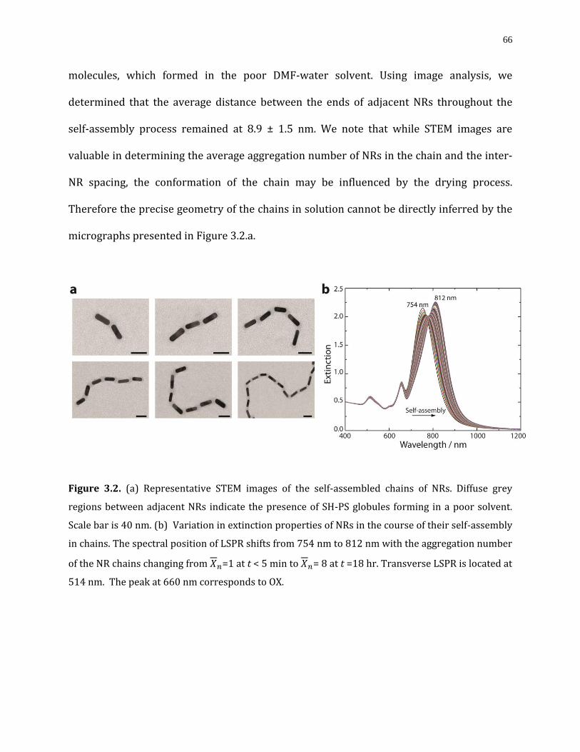
66
molecules, which formed in the poor DMF-water solvent. Using image analysis, we
determined that the average distance between the ends of adjacent NRs throughout the
self-assembly process remained at 8.9 ± 1.5 nm. We note that while STEM images are
valuable in determining the average aggregation number of NRs in the chain and the inter-
NR spacing, the conformation of the chain may be influenced by the drying process.
Therefore the precise geometry of the chains in solution cannot be directly inferred by the
micrographs presented in Figure 3.2.a.
Figure 3.2. (a) Representative STEM images of the self-assembled chains of NRs. Diffuse grey
regions between adjacent NRs indicate the presence of SH-PS globules forming in a poor solvent.
Scale bar is 40 nm. (b) Variation in extinction properties of NRs in the course of their self-assembly
in chains. The spectral position of LSPR shifts from 754 nm to 812 nm with the aggregation number
of the NR chains changing from =1 at t < 5 min to = 8 at t =18 hr. Transverse LSPR is located at
514 nm. The peak at 660 nm corresponds to OX.

67
The growth of NR chains in the course of self-assembly was characterized by the
change in the average aggregation number, :
∑
∑ ( )
where and are the number of NR chains and the total number of NRs in the system,
respectively, and is the number of chains containing NRs. The values of were
calculated by analyzing STEM images of nanostructures formed during the course of self-
assembly experiments. The growth kinetics of the NR chains resembled the evolution of
polymer chains in reaction-controlled step-growth polymerization, as reported in our
earlier work.116 However, the self-assembly of the NRs in the presence of OX occurred at a
greatly increased rate, in comparison with an OX-free system.
The extinction and SERS measurements were carried out throughout the course of
self-assembly (t from 5 min to 18 hrs) with concurrent collection of samples for STEM
imaging. Figure 3.2.b shows the evolution of the extinction spectra of the system
undergoing self-assembly. In the course of chain growth, the longitudinal LSPR peak
shifted from 754 to 812 nm, due to the coupling of alternating dipoles along the NR chain.
The end-to-end arrangement led to the reduction in resonance energy with respect to
individual NRs.24,27,117-120 In the course of self-assembly, the width of the longitudinal LSPR
peak broadened by 12 % when increased from 1 to 8, which was substantially
narrower than for solution-based aggregates of gold NPs reported to date. The absorption
peak at 659 nm corresponded to OX molecules. This peak was not measurably shifted or

68
diminished in intensity for a period of greater than 18 hr, which suggested good structural
and temporal stability of OX during NR self-assembly.
3.2.2. Ensemble-averaged SERS
Figure 3.3.a shows the evolution of the ensemble-averaged SERS spectra of OX
through the course of NR self-assembly. The most enhanced bands at 563 and 604 cm-1
(assigned to vibrational modes of the phenoxazine ring of the dye)121,122 were consistent
with the Raman spectrum of the solution of OX in DMF. The same values of vibrational
frequencies of OX adsorbed on the surface of NRs and of the solution of OX in DMF
suggested that the reporter molecule was physisorbed onto the gold surface.123
Figure 3.3. (a) Evolution of normalized ensemble averaged SERS spectra in self-assembled NR
chains. The average aggregation number of NR assemblies changes from =1 at t < 5 min (bright-
red spectrum) to = 8 at t =18 hr (black spectrum). The SERS peaks at 563 and 604 cm-1 are
normalized against the SERS peak of DMF at 659 cm-1 (indicated with astericks). (b) Variation in the
normalized SERS peak intensity measured at 563 cm-1 plotted as a function of the average

69
aggregation number of the NR chains. SERS variation (y error) is based on three measurements
taken within 15 min. Approximately 1000 NRs (including individual species) were used in the
calculations of number (x error). Laser excitation wavelength was 785 nm.
Next, we considered the local environment of the OX molecules that provided the
main contribution to the overall intensity of SERS. It is possible that OX could be localized
within the CTAB layer (on the NR sides) and/or be associated with SH-PS molecules at the
NR ends. In the first instance, hydrophobic interactions with hydrocarbon chains of CTAB,
could dominate localization of OX since the localization of positively charged OX in the
vicinity of the cationic groups of CTAB was less likely. In the second case, OX could be
associated with the PS, such that the nonpolar component of the dye would interact with
hydrophobic PS molecules while its polar head would remain in the solvent environment.
To address the question of the localization of the dye within the NR chains which
made a predominant contribution to SERS signals, a series of control SERS experiments
were carried out with OX dissolved in several solvents; water, DMF and the DMF/water
mixture (water content 20 vol. %). The experiments were carried out using a roughened
gold substrate. The SERS frequency of the strongest OX band in the 500-600 cm-1 region
was dependent on the solvent type: in water, the SERS band was centered at 595 cm-1,
similar to previously reported results,121,122 and in DMF the spectral position of the peak
was 567 cm-1 (Figure 3.4.).
In the DMF/water mixture the SERS spectrum of OX featured two peaks located at
595 and 567 cm-1 (Figure 3.4). For the self-assembled NR chains, the main SERS peak of OX
was measured at 563 cm-1, that is, very close to 567 cm-1, suggesting that OX was located in
a DMF environment. We note that the absence of a shoulder at 595 cm-1 (Figure 3.4)

70
suggested that no appreciable interactions existed between OX and water. Therefore, it was
reasonable to conjecture that we were probing OX predominately localized within the hot-
spot region between the ends of the NRs from which water is largely excluded. We note
that this did not rule out the possibility of OX molecules being located in the hydrophobic
environment in the CTAB layer. However, the species outside the hot-spots did not
significantly contribute to the overall SERS signal. Furthermore, no change in vibrational
frequency of OX at 563 cm-1 in the course of assembly indicated that the location of
physisorbed OX remained unaltered. The relative intensities of the bands of OX at 563 and
604 cm-1 also remained constant throughout the process of self-assembly, suggesting that
OX retained its orientation and geometry with respect to the NR surface without any
appreciable molecular re-orientation.124,125
Figure 3.4. SER spectra of oxazine 4 µM adsorbed on roughened gold substrate as a function of
solvent environment (a) H2O, (b) DMF and (c) DMF/ H2O mixture containing 20 vol. % of H2O.
71
The change in the SERS intensity was determined over the course of NR self-assembly
by using the intensity of the peak corresponding to DMF vibration at 659 cm-1 as an
internal standard. Figure 3.3.b shows the variation in the ratio of intensities of the peak at
563 cm-1 of OX to the intensity of the peak at 659 cm-1, plotted as a function of .
Importantly, the change in ensemble-averaged normalized SERS intensity was not
monotonic: it increased for 1 ≤ ≤ 3, leveled off when 3 ≤ ≤ 5, and increased again
for 5 ≤ ≤ 8.
To understand this non-linear behavior, we considered only SERS arising from the
electromagnetic effect. Under resonance conditions, the incident light absorbed by the
nanoparticles generates localized surface plasmons, thereby creating a strong local
electromagnetic field, Eloc(ωexc), close to the surface of the NRs. This effect leads to the
enhancement in intensity of the Raman scattered light by the OX molecule which is
assumed to be a point dipole. The scattered light also excites localized surface plasmons
and generates an enhanced field, Eloc(ωRS), at the Raman Stokes frequency. The field
enhancement GSERS is proportional to the square of the product of the local field at the
incident frequency and the local field at the scattered Raman Stokes frequency,126-130 that
is: GSERS |Eloc(ωexc) Eloc(ωRS)|2 (2)
As discussed above, light extinction (absorption + scattering) at wavelengths matching the
resonances of the nanostructure, generate LSPR that leads to field localization. Therefore, a
correlation between the SERS efficiency and the product of extinctions at ωexc and ωRS
should be expected.

72
We plotted the variations in the normalized SERS intensity and the product of the
extinctions measured at the excitation wavelength of 785 nm (ωexc) and at the wavelength
of the Stokes-shifted radiation of 821 nm (ωRS) versus the average aggregation number, ,
of the NR chains (Figure 3.5). In the course of NR self-assembly, the product of extinctions
varied, since the spectral position of the longitudinal LSPR gradually red-shifted (see Figure
3.2).
Figure 3.5. Correlation of the normalized intensity of SERS peak at 563 cm-1 (red circles) and the
product of extinctions measured at 785 and 821 nm (blue circles), plotted as a function of the
aggregation number of the NR chains. Top: y errors of the intensity of SERS peak (red squares)
and the product of extinctions (blue squares) were calculated based on three measurements.
Figure 3.5 shows a strong correlation between the variation in ensemble-averaged
SERS intensity and the product of extinctions, plotted as a function of . Such correlation

73
indicated that the variation in SERS properties with NR assembly, indeed, originated from
the inherent electromagnetic properties of the self-assembled nanostructure, rather than
from chemical effects. In addition, the results shown in Figure 3.5 suggested a narrow
distribution of hot-spots, confirming the high level of organization of the dynamic self-
assembled system in solution. We note that a direct correlation between extinction and
SERS is qualitatively followed in simple nanostructures such as individual gold spheres and
organized arrays,59 but it falls apart dramatically in strongly coupled random systems with
a large distribution of spatially localized resonances.60 Therefore, the results from Figure
3.5 confirm the high level of organization of our system.
3.2.3. Finite-difference Time-domain Simulations
In order to further highlight the relationship between SERS enhancement and the
dynamic evolution of hot-spots, we conducted comprehensive FDTD simulations by
numerically solving Maxwell’s curl equations by iteration over time.131 Figure 3.6 shows
examples of electric field (E field) profiles corresponding to different wavelengths for the
chains of co-linearly assembled NRs. The field inside individual NRs rapidly decayed, while
hot-spots between adjacent NRs exhibited a maximum E field intensity 4000-fold greater
than the intensity of the incident field.

74
Figure 3.6. Three-dimensional finite-difference time-domain (3D-FDTD) simulation of the end-to-
end assembly of gold NRs. Electric field profile was calculated at the resonance wavelength of the
co-linear NR chain at (a) 760 nm, (b) 782 nm, and (c) 802 nm. Polarization of the incident light is
parallel to the long axes of the NRs (i.e., to the z-coordinate). Hot-spots between adjacent NRs show
a maximum electric field intensity 4000 times greater than the incident field.
In our work, the self-assembled NR chains were characterized by the distribution of
their aggregation numbers and the variation in the angle between adjacent NRs within the
chain. In order to examine the role of the distribution in of the NR chains, we performed
FDTD simulations for chains with different lengths, and then used experimentally
determined aggregation statistics to calculate the E field intensities (Figure 3.7). For = 8
the sum of E field intensity squared had the largest value when normalized with respect to
the aggregation number of the chain (Figure 3.7a), which was consistent with experimental
results shown in Figure 3.3. When the populations of NRs are not mixed (ideal case) the
longer chains had a lower maximum intensity, they also had less variation in their
maximum intensity wavelength, compared to the shorter chains (Figure 3.7b). The highest
E field intensity observed when = 8 may be due to the relatively high spectral purity at
this degree of the assembly.
When the distribution in the aggregation numbers was not taken into account, the
field intensity was highest for chains containing three NRs when normalizing to the
number of NRs in the chain (Figure 3.7b). This effect originated from the trade-off between

75
the local field enhancement and optical absorption (that is, loss) in the NR chains. A figure
of merit that compares the local field enhancement to the loss is the ratio between the real
and imaginary parts of the relative permittivity of the NRs. For gold, this figure of merit is
at maximum at ~770 nm, which was close to the resonance wavelength of the trimer.
Figure 3.7. FDTD simulation showing (a) Electric field intensity squared obtained from
incorporating average NR aggregation number, as a function of wavelength (factoring in
experimentally determined statistical data) (b) Normalized sum of electric field intensity squared
over a small volume enclosing the NR chain, for ideal NR chain lengths (Standard deviation is equal
to zero) ranging from 1 to 9 NRs as a function of wavelength. (c) Sum of electric field intensity
squared over a small volume enclosing NRs, chain lengths (number of NRs ranging from 1 to 9) as a
function of wavelength (not normalized). (d) Peak electric field intensity squared values plotted

76
against their corresponding resonant wavelengths. Number of NRs increases from 1 to 9 (left to
right).
Since the SERS and LSPR properties of the NR assemblies depend on the co-linearity
of the NRs with respect to the long axis of the chain,32,33,48 we have performed FDTD
calculations for dimers and trimers of NRs with different orientations with respect to each
other (Figure 3.8). The deviation from co-linearity at the angles between the long axes of
the NRs of 20, 40, 60 and 90o resulted in a significant reduction of extinction and thus,
decrease in E field intensity (Figure 3.8). This result implied that in ensemble
measurements, the greatest contribution in extinction and SERS arose from co-linear chain
conformations, with a minor influence on E field intensity from off-axis NRs.

77
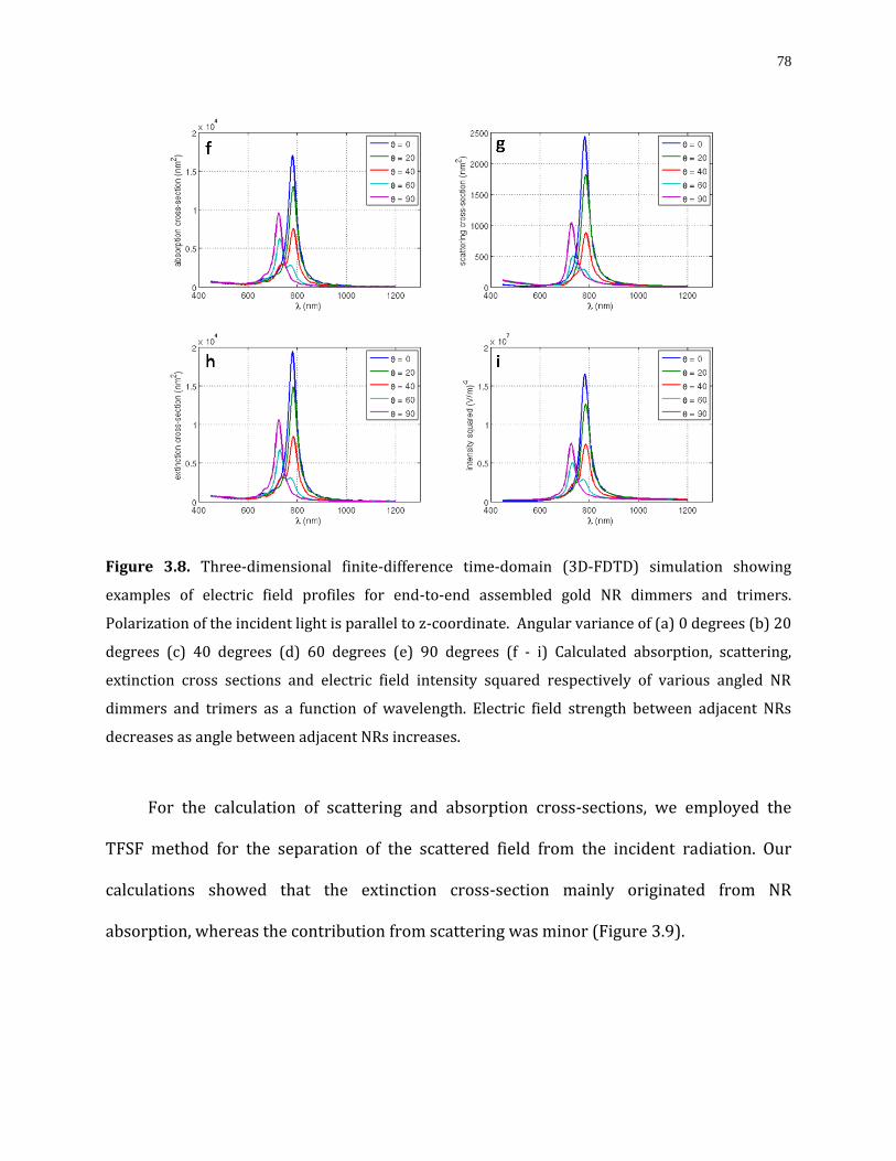
78
Figure 3.8. Three-dimensional finite-difference time-domain (3D-FDTD) simulation showing
examples of electric field profiles for end-to-end assembled gold NR dimmers and trimers.
Polarization of the incident light is parallel to z-coordinate. Angular variance of (a) 0 degrees (b) 20
degrees (c) 40 degrees (d) 60 degrees (e) 90 degrees (f - i) Calculated absorption, scattering,
extinction cross sections and electric field intensity squared respectively of various angled NR
dimmers and trimers as a function of wavelength. Electric field strength between adjacent NRs
decreases as angle between adjacent NRs increases.
For the calculation of scattering and absorption cross-sections, we employed the
TFSF method for the separation of the scattered field from the incident radiation. Our
calculations showed that the extinction cross-section mainly originated from NR
absorption, whereas the contribution from scattering was minor (Figure 3.9).

79
Figure 3.9. Calculated absorption, scattering and extinction cross sections as a function of
wavelength for various NR chain lengths ((a) to (c) respectively) and average NR aggregation
number ((d) to (f) respectively). A total-field scattered field (TFSF) source is utilized for calculating
the scattering and absorption cross-sections. Incident field polarization is parallel to the major rod
axis (i.e. z), the bandwidth of source is from 600 nm to 1000 nm. Simulation domain is terminated

80
with perfectly matched layer (PML). A mesh override region of (1 nm x 1nm x 1nm) mesh size is
defined for better modeling of the circular rods in Cartesian coordinates. A 3-D time domain
monitor is utilized for recording the field strengths as a function of time and a Fourier transform
provides the frequency domain results. Extinction cross-section were calculated for different NR
chain lengths and a certain factor (see main text) from each curve was added according to the
experimental statistical data to lead figure (f). The heterogenity of NR chain size at each stage of the
assembly is one of the contributing factors to variations in the observed amplitude.
Experimental and calculated results obtained for the extinction (Figure 3.9) and
variations in the spectral position of the longitudinal LSPR (Figure 3.10a) were in good
agreement when NR number distribution was considered. Figure 3.10b shows the change
in the calculated extinctions (product of 785 and 821 nm) and E field intensity squared as a
function of . A strong correlation between the two trends was consistent with the
relationship expressed in Equation (2). Significantly, the experimental results (Figure 3.5)
and theoretical results shown in Figure 3.10(b) were found to be in good qualitative
agreement.
Figure 3.10. (a) Variation in experimentally measured (blue circles) and calculated (red squares)
spectral position of the longitudinal LSPR plotted as a function of the average aggregation number,
, of the NR chains. (b) Variation in the calculated product of the squares of the electric field

81
(intensity) at 785 nm and 821 nm (red circles) and the product of the extinction cross-sections at
785 nm and 821 nm (blue circles), plotted vs. .
3.3. Summary and Conclusions
Following dynamic generation of hot-spots via controlled, solution-based self-assembly of
gold NR chains, (1) we have established a direct relationship between extinction and SERS
properties of the chains. An important aspect of our work included the formation of ensembles
with well-defined, invariant distance between adjacent NRs. (2) Our FDTD calculations
showed that as NR chains get longer (Xn > 3) the sum of E-field intensity squared decreases
due to a trade-off between the local field enhancement and optical absorption in the NR
chains. However, measured ensemble-averaged SERS intensity was the highest at = 8 as
a consequence of a reduced NR population spread resulting in higher spectral purity. (3)
Factoring in the observed chain length distribution over time, it was possible to reconcile
observation and calculation data. (4) The observed ensemble-averaged SERS signals were
intentionally modest in order to probe the dynamic generation of hot-spots in solution
state assembly. This was achieved by carefully balancing experimental parameters.
Our work opens the way for studies of optical properties of other geometry-dependent
dynamic plasmonic systems, e.g., ensembles of side-by-side gold NRs and compartmentalization
of molecules or particles using hot spots. Building from the correlation between SERS and
extinction, practical applications of self-assembled structures ranging from chemical and
biological sensing to nanoelectronics, e.g., plasmonic circuits, become a step closer.

82
References
(1) Claridge, S. A.; Castleman, A. W.; Khanna, S. N.; Murray, C. B.; Sen, A.; Weiss, P. S. ACS
Nano 2009, 3, 244–255.
(2) Glotzer, S. C.; Solomon, M. J. Nat. Mater. 2007, 6, 557–562.
(3) Grzelczak, M.; Vermant, J.; Furst, E. M.; Liz-Marzan, L. M. ACS Nano 2010, 4, 3591–3605.
(4) Mann, S. Nat. Mater. 2009, 8, 781–792.
(5) Nie, Z. H.; Petukhova, A.; Kumacheva, E. Nat. Nanotech. 2010, 5, 15–25.
(6) Srivastava, S.; Kotov, N. A. Soft Matter 2009, 5, 1146–1156.
(7) Lee, A.; Coombs, N. A.; Gourevich, I.; Kumacheva, E.; Scholes, G. D. J. Am. Chem. Soc.
2009, 131, 10182–10188.
(8) Tang, Z. Y.; Zhang, Z. L.; Wang, Y.; Glotzer, S. C.; Kotov, N. A. Science 2006, 314, 274–278.
(9) Shevchenko, E. V.; Talapin, D. V.; Kotov, N. A.; O’Brien, S.; Murray, C. B. Nature 2006, 439,
55–59.
(10) Zhang, S. Z.; Kou, X. S.; Yang, Z.; Shi, Q. H.; Stucky, G. D.; Sun, L. D.; Wang, J. F.; Yan, C. H.
Chem. Commun. 2007, 1816–1818.
(11) Zhuang, J. Q.; Wu, H. M.; Yang, Y. A.; Cao, Y. C. J. Am. Chem. Soc. 2007, 129, 14166-
14167.
(12) Jones, M. R.; Macfarlane, R. J.; Lee, B.; Zhang, J. A.; Young, K. L.; Senesi, A. J.; Mirkin, C. A.
Nat. Mater. 2010, 9, 913–917.
(13) Wang, Z. L. Adv. Mater. 2003, 15, 432–436.
(14) Tseng, R. J.; Tsai, C. L.; Ma, L. P.; Ouyang, J. Y. Nat. Nanotech. 2006, 1, 72–77.
(15) Lee, J.; Hernandez, P.; Govorov, A. O.; Kotov, N. A. Nat. Mater. 2007, 6, 291–295.

83
(16) Desvaux, C.; Amiens, C.; Fejes, P.; Renaud, P.; Respaud, M.; Lecante, P.; Snoeck, E.;
Chaudret, B. Nat. Mater. 2005, 4, 750–753.
(17) Sonnichsen, C.; Reinhard, B. M.; Liphardt, J.; Alivisatos, A. P. Nat. Biotechnol. 2005, 23,
741–745.
(18) Sun, S. H.; Murray, C. B. J. Appl. Phys. 1999, 85, 4325–4330.
(19) Brown, L. V.; Sobhani, H.; Lassiter, J. B.; Nordlander, P.; Halas, N. J. ACS Nano 2010, 4,
819–832.
(20) Liu, J. W.; Lu, Y. J. Am. Chem. Soc. 2003, 125, 6642–6643.
(21) Denisyuk, A. I.; Adamo, G.; MacDonald, K. F.; Edgar, J.; Arnold, M. D.; Myroshnychenko,
V.; Ford, M. J.; de Abajo, F. J. G.; Zheludev, N. I. Nano Lett. 2010, 10, 3250–3252.
(22) Alivisatos, A. P.; Johnsson, K. P.; Peng, X. G.; Wilson, T. E.; Loweth, C. J.; Bruchez, M. P.;
Schultz, P. G. Nature 1996, 382, 609–611.
(23) Chen, C. L.; Zhang, P. J.; Rosi, N. L. J. Am. Chem. Soc. 2008, 130, 13555–13557.
(24) Mirkin, C. A.; Letsinger, R. L.; Mucic, R. C.; Storhoff, J. J. Nature 1996, 382, 607–609.
(25) Chen, C. L.; Rosi, N. L. J. Am. Chem. Soc. 2010, 132, 6902–6903.
(26) Zubarev, E. R.; Xu, J.; Sayyad, A.; Gibson, J. D. J. Am. Chem. Soc. 2006, 128, 15098–
15099.
(27) Caswell, K. K.; Wilson, J. N.; Bunz, U. H. F.; Murphy, C. J. J. Am. Chem. Soc. 2003, 125,
13914–13915.
(28) (a) Nie, Z. H.; Fava, D.; Kumacheva, E.; Zou, S.; Walker, G. C.; Rubinstein, M. Nat. Mater.
2007, 6, 609–614. (b) Nie, Z.; Fava, D.; Winnik, M. A.; Rubinstein, M.; Kumacheva, E. J. Am.
Chem. Soc. 2008,130, 3683–3689.
(c) Fava, D.; Nie, Z.; Winnik, M. A.; Kumacheva, E. Adv. Mater. 2008, 20, 4318–4322.

84
(29) Joseph, S. T. S.; Ipe, B. I.; Pramod, P.; Thomas, K. G. J. Phys. Chem. B 2006, 110, 150–
157.
(30) Jain, P. K.; Eustis, S.; El-Sayed, M. A. J. Phys. Chem. B 2006, 110, 18243–18253.
(31) Link, S.; Mohamed, M. B.; El-Sayed, M. A. J. Phys. Chem. B 1999, 103, 3073–3077.
(32) Slaughter, L. S.; Wu, Y. P.; Willingham, B. A.; Nordlander, P.; Link, S. ACS Nano 2010, 4,
4657–4666.
(33) Funston, A. M.; Novo, C.; Davis, T. J.; Mulvaney, P. Nano Lett. 2009, 9, 1651–1658.
(34) Addison, C. J.; Brolo, A. G. Langmuir 2006, 22, 8696–8702.
(35) Hu, X; Cheng, W; Wang, T; Wang, Y; Wang, E; S, D. J. Phys. Chem. B 2005, 109, 19385–
19389.
(36) Nikoobakht, B.; El-Sayed, M. A. J. Phys. Chem. A 2003, 107, 3372–3378.
(37) Chen, G.; Wang, Y.; Tan, L. H.; Yang, M. X.; Tan, L. S.; Chen, Y.; Chen, H. Y. J. Am. Chem.
Soc. 2009, 131, 4218–4219.
(38) Goddard, G.; Brown, L. O.; Habbersett, R.; Brady, C. I.; Martin, J. C.; Graves, S. W.; Freyer,
J. P.; Doorn, S. K. J. Am. Chem. Soc. 2010, 132, 6081–6090.
(39) Laurence, T. A.; Braun, G.; Talley, C.; Schwartzberg, A.; Moskovits, M.; Reich, N.; Huser,
T. J. Am. Chem. Soc. 2009, 131, 162–169.
(40) Chen, T.; Wang, H.; Chen, G.; Wang, Y.; Feng, Y. H.; Teo, W. S.; Wu, T.; Chen, H. Y. ACS
Nano 2010, 4, 3087–3094.
(41) Felidj, N.; Aubard, J.; Levi, G.; Krenn, J. R.; Hohenau, A.; Schider, G.; Leitner, A.;
Aussenegg, F. R. Appl. Phys. Lett. 2003, 82, 3095–3097.
(42) Felidj, N.; Aubard, J.; Levi, G.; Krenn, J. R.; Salerno, M.; Schider, G.; Lamprecht, B.;
Leitner, A.; Aussenegg, F. R. Phys. Rev. B 2002, 65, 075419.

85
(43) Nikoobakht, B.; El-Sayed, M. A. Chem. Mater. 2003, 15, 1957–1962.
(44) Taflove, A.; Hagness, S. C. Computational Electrodynamics: The Finite-Difference Time
Domain Method, 2nd ed.; Artech House: Boston, 2000.
(45) Johnson, P. B.; Christy, R. W. Phys. Rev. B 1972, 6, 4370–4379.
(46) Liu, K.; Nie, Z. H.; Zhao, N. N.; Li, W.; Rubinstein, M.; Kumacheva, E. Science 2010, 329,
197–200.
(47) Prodan, E.; Nordlander, P. J. Chem. Phys. 2004, 120, 5444–5454.
(48) Tabor, C.; Van Haute, D.; El-Sayed, M. A. ACS Nano 2009, 3, 3670–3678.
(49) Shao, L.; Woo, K. C.; Chen, H. J.; Jin, Z.; Wang, J. F.; Lin, H. Q. ACS Nano 2010, 4, 3053–
3062.
(50) Brolo, A. G.; Sanderson, A. C. Can. J. Chem. 2004, 82, 1474–1480.
(51) Brolo, A. G.; Sanderson, A. C.; Smith, A. P. Phys. Rev. B 2004, 69, 045424.
(52) Aroca, R. Surface-enhanced vibrational spectroscopy; John Wiley & Sons: New York,
2006.
(53) Moskovits, M. J. Chem. Phys. 1982, 77, 4408–4416.
(54) Moskovits, M.; Suh, J. S. J. Phys. Chem. 1984, 88, 5526–5530.
(55) Kneipp, K.; Kneipp, H.; Itzkan, I.; Dasari, R. R.; Feld, M. S. Chem. Rev. 1999, 99, 2957–
2975.
(56) Moskovits, M. Rev. Mod. Phys. 1985, 57, 783–826.
(57) Schatz, G. C.; Young, M. A.; Van Duyne, R. P. In Surface- Enhanced Raman Scattering:
Physics and Applications, Topics in Applied Physics 103; Kneipp, K., Moskovits, M., Kneipp,
H., Eds.; Springer: Berlin, 2006; pp 19-45.
(58) Weitz, D. A.; Garoff, S.; Gersten, J. I.; Nitzan, A. J. Chem. Phys. 1983, 78, 5324–5338.

86
(59) Kelly, K. L.; Coronado, E.; Zhao, L. L.; Schatz, G. C. J. Phys. Chem. B 2003, 107, 668–677.
(60) Le Ru, E. C.; Galrefloway, C.; Etchegoin, P. G. Phys. Chem. Chem. Phys. 2006, 8, 3083–
3087.
87
Chapter 4
Probing Side-by-side Assembled Gold
Nanorods via Ensemble-averaged SERS
There is often a misconception that aggregates of metal nanoparticles are better
surface-enhanced Raman scattering (SERS) probes than individual nanoparticles. We show
that for asymmetric particles such as gold nanorods (NRs) this is not always the case as the
plasmonic behavior of NR ensembles depends on the architecture of the ensemble, that is,
on the mutual orientation of the NRs. We report experimental and theoretical analysis of the
optical properties of side-by-side assembled gold NRs. Extinction measurements and ensemble-
averaged SERS spectroscopy showed a blue shift of the surface plasmon resonance and a
reduction of SERS intensity respectively. Comprehensive Finite-Difference Time-Domain
(FDTD) simulations showed a reduction of electric field intensity as the number of NRs per
cluster increased due to the radial component of electric field cancellation leading to “destructive
interference”. A further understanding of a blue shift of the surface plasmon resonance in the
side-by-side assembled NR structures is explained by the propagation constant of the surface
plasmon mode.
The present work expands our understanding of configuration-specific optical
behavior of gold NRs in a solution state. Furthermore, this study offers guidance towards

88
the establishment of “design rules” for the development of colloidal NR systems for
plasmonic sensing applications.
4.1. Introduction
The utilization of light-metal interactions on the nanoscale has shown great promise
in nanoantennas,1-5 extraordinary transmission,6,7 and plasmonic waveguides,8-10 all
achieved through precise “top-down” control of geometry, size and composition of metallic
nanostructures. In parallel to these fabrication approaches, “bottom-up” methods for
employing colloidal metallic nanoparticles (MNPs) are receiving increasing attention,
because of their relative low cost and potential use for “bio-sensing” in-vivo.
One of the important applications of the plasmonic properties of MNPs is their
utilization in surface-enhanced Raman scattering (SERS). SERS provides structural
information about analytes adsorbed on the surface of MNPs and exceptionally high sensitivity
as compared to ordinary Raman scattering.11-13 The amplification of Raman intensity arises
from local electromagnetic fields resulting from the surface plasmon resonance (SPR) of
MNPs. The magnitude of the Raman scattering from analytes adsorbed or close to the
surface of MNPs is approximately proportional to the fourth power of the local field when
the electromagnetic mechanism of SERS is considered.11,14,15
The spectral position of the SPR of MNPs can be tuned by varying the dimensions
and shapes of MNPs, along with the nature of the medium surrounding them. There is also
significant interest in ensembles of MNPs, owing to the coupling of plasmons of adjacent
particles.9,16 Structural, configuration-dependent, plasmonic behavior of ensembles of

89
MNPs can affect both the intensity and the spectral position of SPR wavelength, thereby
providing greater insight into the plasmon coupling phenomena.
Gold NRs are of particular interest because of their intrinsic shape-anisotropy. They
exhibit transverse and longitudinal SPR modes corresponding to the coherent electron
oscillations perpendicular and parallel to the long NR axis, respectively.17 This NR feature
offers spectral tunability of the longitudinal SPR in the near-IR region, thereby offering
potential applications in the “biological window” range.18,19 In addition, in their ensembles,
gold NRs can exhibit a well-defined mutual alignment in a side-by-side or end-to-end
manner. The plasmon coupling between gold NRs in their ensembles depends not only on
the interparticle distance but also, on the mutual orientation of the NRs with respect to
each other. Therefore, gold NRs are well-suited to study the optical properties of
aggregated NP systems.
To date, the majority of experimental studies of SERS properties of clusters of MNPs
have been carried out for irregular, aggregated systems. These aggregate structures led to
significant variability of their optical properties. As a result, there remains an insufficient
understanding of the influence of the architecture of aggregates of MNPs on their SERS
properties, particularly in a solution state. As such, research has focused on the study of
isolated NP aggregates. Specifically, the optical properties of isolated dimers of NRs in a dry
state, that were arranged in the end-to-end, side-by-side, L-shape or T-shaped manner have
been investigated via “single-particle” scattering measurements.20,21 The experimental
results showed that the scattering intensity of dimers is dependent on the polarization
direction of the incident light, so that the maximum intensity is reached when the
polarization is parallel to the long axis of the NRs. These experimental findings were in

90
good agreement with calculations of plasmon hybridization and Finite-Difference Time-
Domain (FDTD) simulations.20 A study of the effect of the angular orientations of NRs in the
dimers fabricated by electron beam lithography with separations no smaller than 20 nm showed
plasmon coupling dependence on NR orientation, separation, induced dipole strength and the
dielectric constant of the medium.22 “Single-particle” measurements of scattering,
extinction and SERS of NR dimers and a theoretical explanation of geometry-specific NR
assembly23 have provided deeper insights into the optical behavior of isolated NP
aggregates. However, the understanding of the properties of ensemble-averaged system
behavior, factoring in aggregate populations, SPR shift and E field distribution in a dynamic
solution state, remains challenging. A small piece of this puzzle has been addressed in
Chapter 4, where the optical properties of ensembles of NRs arranged in an end-to-end
manner were explored.24 We studied the highly localized electric field (E field) intensity
regions (“hot spots”) that were generated between the ends of adjacent NRs.25,26 We
showed a direct correlation between extinction and ensemble-averaged SERS as a function
of the average aggregation number of NR end-to-end assembly.24 The calculated,
normalized E field intensity showed a decrease as the average length of NR chains
increased, which may be due to a “trade-off” between the loss and the local field
enhancement. For this end-to-end configuration where the E field is oriented along the NR
axis, the near E fields couple in a manner analogous to a “bonding” interaction resulting in a
red-shift of the longitudinal SPR.20,21
The side-by-side assembly of gold NRs has been achieved via attractive forces
between the ligands coating the long side of the NRs, namely, chelating agents,27 an
antibody of a toxin molecule (microcystin-LR),28and the addition of anions via electrostatic

91
interactions (citrate).29 Currently, a single experimental study exists that reports on the
solution state SERS properties of side-by-side assembled NRs. This study showed a 10-fold
increase in intensity of SERS signals by using a resonant dye as compared to the SERS of the
individual NRs.29
Additionally, 3D multilayered stacks and 2D sheets of side-by-side assembled NRs
are highly SERS active.27,30,31 We note that 3D and 2D superstructures give a distinct E-field
distribution and consequently, different SERS properties as compared to side-by-side
assembled clusters in solution. For example, a micrometer-sized 3-D NR stack consisting of
~15 layers of NRs can be realized as a highly efficient SERS substrate. The simulated E field
intensity is higher for the 3 layered NR stacks as compared to the 1 layered. This may be
due to the field enhancement in the gap between the layers.31 Another report showed that a
side-by-side assembled sheet-like micrometer -sized structure (2D) showed a high SERS
activity likely due to the very large population of constituent NRs thus, producing larger
number of hot-spots27.
We hypothesized that in clusters of side-by-side aligned NRs, since plasmons of NRs
interact with each other in an “anti-bonding” mode (leading to a blue shift of the
longitudinal SPR of the NRs in their ensembles), the local E-field should decrease (Figure
4.1). Consequently, the intensity of SERS should also decline, if it originates from
electromagnetic effects. To test our hypothesis, we examined theoretically and
experimentally the optical properties of gold NRs assembled in the side-by-side fashion.
We simulated E-field distribution and extinction (absorption + scattering) of the clusters of
side-by-side assembled NRs via the Finite-Difference Time-Domain (FDTD) method. We
numerically solved Maxwell’s curl equations by iteration over time.32 Experimentally, we

92
examined the extinction and ensemble-averaged SERS properties of the NR clusters
following their assembly in a solution state.
Figure 4. 1. Schematic illustration of gold nanorods (NRs) assembled in a side-by-side
manner showing a reduction of electric field as the number of NRs increases in the NR
ensembles.

93
4.2. Results and Discussion
4.2.1. Finite-difference Time-domain Simulations
Figure 4.2 (a-c) shows FDTD calculations of the change in the normalized
absorption, scattering and extinction cross-sections, all plotted as a function of wavelength
for NR assemblies in side-by-side conformations containing from 1 to 8 NRs. For the
complex permittivity of gold, we used the experimental data of Johnson and Christy.33 The
simulation domain was terminated by perfectly matched layer to ensure minimum
reflections. Total field scattered field (TFSF) source was used for the determination of
absorption, scattering and extinction cross-sections of assembled NRs. TFSF divides the
simulation domain into two regions. In one region, only scattered fields are present while
the other region contains both the incident and scattered fields. Scattering cross-section
was determined by calculating the Poynting vector over a closed surface surrounding the
NRs in the scattered field region. Absorption cross-section was calculated by determining
the net flow of power into a closed surface surrounding the NRs in the total field region.
The incident plane wave was polarized at 45 degrees to the long axis of the NRs and as
such, this polarization probes both the transverse and longitudinal modes. The mesh
override region was defined with a mesh size of 1 nm for accurate modeling of the
cylindrical structure in a Cartesian coordinate system.
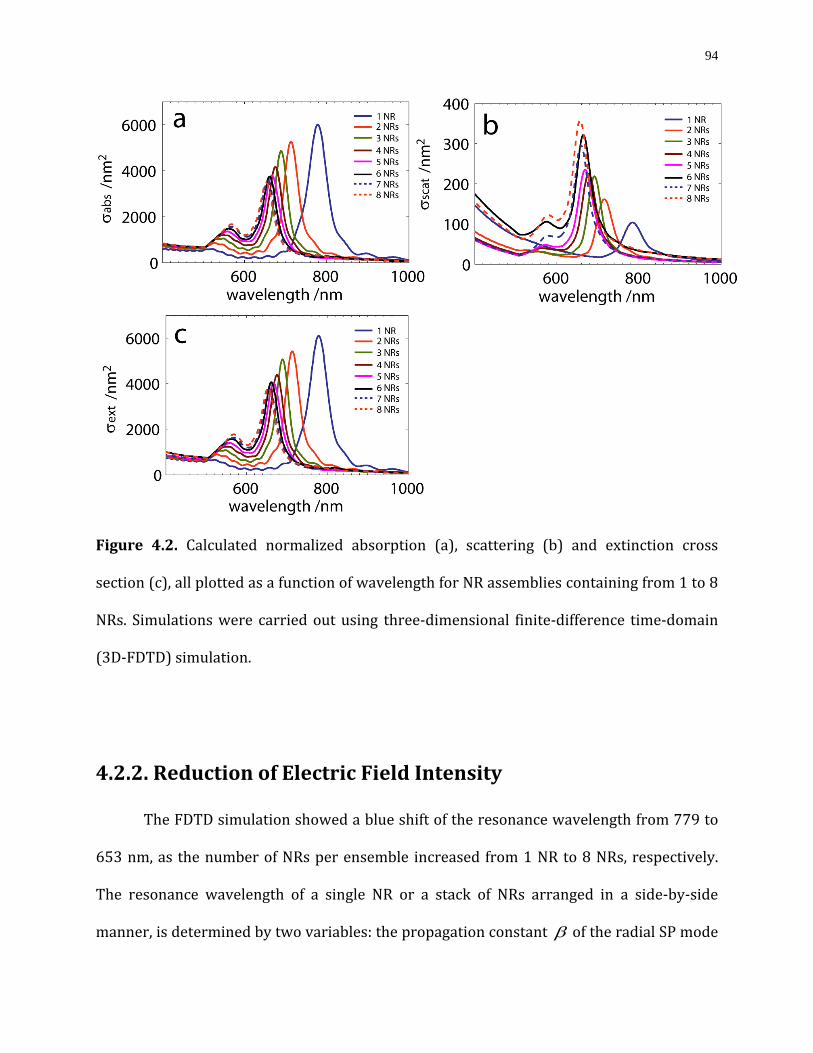
94
Figure 4.2. Calculated normalized absorption (a), scattering (b) and extinction cross
section (c), all plotted as a function of wavelength for NR assemblies containing from 1 to 8
NRs. Simulations were carried out using three-dimensional finite-difference time-domain
(3D-FDTD) simulation.
4.2.2. Reduction of Electric Field Intensity
The FDTD simulation showed a blue shift of the resonance wavelength from 779 to
653 nm, as the number of NRs per ensemble increased from 1 NR to 8 NRs, respectively.
The resonance wavelength of a single NR or a stack of NRs arranged in a side-by-side
manner, is determined by two variables: the propagation constant of the radial SP mode

95
and the phase of light reflection from the ends of the NRs. At resonance, the following
condition must be satisfied:
(1)
where L is the NR length, ref is the phase of reflection from the end of the NRs, and is the
propagation constant ( where is the effective index of the system
containing NRs and the surrounding medium). The analytical expression for the phase of
reflection from flat-ended NRs has recently been derived,34 whereas only numerical
solutions for phase of reflection for NRs with hemispherical ends (common in colloidal
systems) are currently available.
The value of is a geometry-dependent variable and it can be obtained from the
mode shape of the radial SP wave. Figure 4.3 shows mode shapes of 1 NR and side-by-side
assemblies of 2 and 3 NRs. By using modal solutions, we numerically verified that as the
number of NRs increases in the ensembles, decreases, thereby reducing .
Specifically, for 1, 2 and 3 NRs, the resultant was 11.81, 9.29 and 8.13, respectively,
and the corresponding value of was 98.9 × 10⁶, 77.8 × 10⁶ and 68.1 × 10⁶ m-1,
respectively. This reduction occurred when the NRs are brought into close proximity to
each other in the side-by-side ensembles. Consequently, the mode shape of interacting NRs
changed as compared to an individual NR. The radial components of the E field of the
neighboring NRs cancel each other due to “destructive interference”, resulting in a
reduction of the local E field. In order to satisfy Equation (1), the reduction in must be
compensated by a proportional amount of reduction in the resonant wavelength. Therefore,

96
a blue shift occurs as the number of NRs increases in side-by-side assembly. It should be noted
that which is weakly wavelength-dependent to first order approximation.34
Figure 4.3. Modes supported by side-by-side assembly of NRs. Mode shapes of surface
plasmons of 1 to 3 NRs from left to right. The resulting effective index values are used for
the calculation of propagation constant of surface wave in the different geometries. Fields
are normalized to their maximum intensities.
Figure 4.4 (a-e) shows examples of FDTD simulations of E field profiles of ensembles
containing from 1 to 5 NRs at their corresponding resonance wavelengths. We note that
the field intensity in the gap between two neighboring NRs is significantly smaller,
compared to the field intensity for a single NR. Figure 4.4 (e) shows the normalized sum of
E field intensity squared as a function of wavelength. As the number of NRs per stack
increases from 1 to 8, the sum of the intensity squared decreases. The reduction of the field
originates from cancellation of the radial component of the SP mode leading to the
“destructive interference” shown in Figure 4.3.
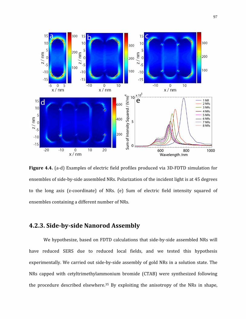
97
Figure 4.4. (a-d) Examples of electric field profiles produced via 3D-FDTD simulation for
ensembles of side-by-side assembled NRs. Polarization of the incident light is at 45 degrees
to the long axis (z-coordinate) of NRs. (e) Sum of electric field intensity squared of
ensembles containing a different number of NRs.
4.2.3. Side-by-side Nanorod Assembly
We hypothesize, based on FDTD calculations that side-by-side assembled NRs will
have reduced SERS due to reduced local fields, and we tested this hypothesis
experimentally. We carried out side-by-side assembly of gold NRs in a solution state. The
NRs capped with cetyltrimethylammonium bromide (CTAB) were synthesized following
the procedure described elsewhere.35 By exploiting the anisotropy of the NRs in shape,

98
surface energy and crystal facet,36-38 we carried out site-specific CTAB exchange at the NR
ends with an SH end-terminated polystyrene (SH-PS) (the molecular weight of SH-PS was
12,000 g/mol and polydispersity index was 1.09).39 These PS-functionalized NRs can be
viewed as an “amphiphilic” building block with a hydrophilic long side and hydrophobic
end-groups. Later in the text, we refer to the PS-functionalized NRs as “NRs”, unless
otherwise stated. To these NRs dissolved in tetrahydrofuran (THF), a solution of Raman
reporter, Cresyl Violet (CV) was introduced dropwise to a final CV concentration of 3 µM,
and the solution mixture was equilibrated for 1 hr.
We triggered the self-assembly of the NRs in a side-by-side manner by changing the
quality of solvent for the ligands. We note that THF is a poor solvent for CTAB, and the
stability of the NRs in THF was attributed to the polystyrene ligands (the values of the
second virial coefficient, A2, is 9.0×10⁻⁴ mol cm3 g−2, equivalent to Flory–Huggins
interaction parameter 0.4).39 We added water to the THF solution of the NRs to a total
concentration of water of 10 wt %, thereby reducing the solubility of the PS ligands. As a
result, the NRs assembled in the side-by-side manner (Figure 4.5).
Figure 4.5. Schematic illustration of side-by-side NR assembly. A thiolated polystyrene
(SH-PS) is attached to the ends of cetyltrimethylammonium bromide (CTAB) coated gold

99
NRs in THF via site-specific ligand functionalization. After the addition of the Raman
reporter, side-by-side assembly was triggered by the addition of water (10 vol. %).
4.2.4. Extinction and TEM Analysis
Figure 4.6 (a) shows photographs of the solutions of NRs following their self-
assembly over time. The typical color of the solutions changed from reddish-purple to
blue, due to an “anti-bonding” interaction20,23 suggesting the side-by-side organization of
the NRs. The side-by-side assembled NRs showed colloidal and temporal stability for 3
months. Figure 4.6 (b) shows the evolution of extinction spectra of NRs self-assembling in
solution, plotted over the course of NR self-assembly. The consistent blue-shift of the
longitudinal SPR peak indicated that the NR assemblies in solution were relatively
monodisperse without the presence of peak broadening, typically seen with larger,
irregular NR aggregates. The longitudinal SPR showed a blue shift from 770 to 715 nm,
exhibiting the trend presented in the FDTD simulations. The blue shift occurred due to the
parallel alignment of dipole modes of individual NRs.20 This configuration has a higher
energy, in comparison with the “bonding” mode, that is, the NRs in the end-to-end
alignment. The transverse SPR showed a relatively small red shift from 510 to 519 nm also in
agreement with the FDTD results. It should be noted that the relatively low intensity of the
transverse SP modes, which interact attractively, leads to the observed red-shift.
Representative scanning transmission electron microscopy (STEM) images of the
NR assemblies in various stages of self-assembly are shown in Figure 4.6 (a).40

100
Figure 4.6. (a) A photograph showing the typical change in color of self-assembling NRs in solution
as a function of time (Top left). Representative scanning transmission electron microscopy (STEM)
images of NRs in various stages of self-assembly. Scale bar is 15 nm (b) Variation in extinction
properties of NR ensembles over time.
A low magnification and additional STEM images of the NR assemblies are shown in Figure
4.8. Using image analysis, we determined that throughout the self-assembly process the
average distance between the long sides of adjacent NRs remained at 1.97 ± 0.48 nm. The
inter–NR spacing was smaller than would be expected for four layers of CTAB ligands (~ 4
nm, assuming capping of the NR sides with a CTAB bilayer).41,42 It is known that when the
solvent evaporates, the NRs are brought together and CTAB molecules are forced to
overlap or inter-digitate driving van der Waals interactions.41,43-45 In addition, STEM
presents projected inter-NR distance, rather than the actual distance. As such, since the
majority of side-by-side NR stacks will not deposit on the substrate such that they are
perpendicular to the incident electron beam, the observed interparticle distance may not
reflect that present in solution. We also note that the precise geometry of the stacks in
solution state may not be directly inferred by the STEM images.
101
By comparing the experimental and simulation results for the case of 1 NR, we observed
a small difference in spectral position and relative intensity of the transverse SPR. The SPR
modes are dependent on the direction of propagation of incident radiation. We explain this
difference as follows. The SPR modes are dependent on the direction of propagation of
incident radiation. The simulations were carried out for one direction of propagation
incident wavevector (kinc) which was perpendicular to the long axis of the NRs. This was
not the case for the extinction experiments carried out for the NR solution. To verify the
dependence on the propagation direction, we conducted simulations with kinc parallel to
the NR axis that is z-propagation. Figure 4.7 shows a comparison of simulation results
carried out with two different directions of propagation that is parallel (z-propagation) and
perpendicular (y-propagation) to the long axis of NRs. These simulations were carried out
for a stack of 2 NRs. It should be noted that for the case of the parallel propagation, only
transverse SPR is excited. The results of absorption, scattering and extinction cross-
sections and the sum of intensity squared of 2 NRs showed the presence of the transverse
SPR at 520 nm.

102
Figure 4.8. Representative scanning transmission electron microscopy (STEM) images of NRs in
various stages of side-by-side assembly. Recorded on a Hitachi S-5200 scanning electron
microscope operating in STEM mode. Note: as-synthesized NRs contain a small population of
spheroids (~5%).

103
Figure 4.7. FDTD simulations showing absorption, scattering, and extinction of 2NRs per stack for
y and z directions of propagation of incident radiation. When wave vector inck
is parallel to the NR
axis, a peak at 520 nm is observed corresponding to the transverse SPR.
We did not attempt to calculate the average aggregation number of the NR ensembles
because it is well-known that upon evaporation of the solvent on a carbon coted TEM grid,
gold NRs form stacks in which they are aligned in the parallel manner. In this case, NRs
interact via van der Waals forces.43 Based on Hamaker integral approximation,46 assuming
NR separation distance d is small ( ≪ ≪ where a is 1/2 of the diameter of the NR
and L is the length of the NR), side-by-side configuration is preferred if the ratio of van der
Waals potential for side-by-side and end-to-end configuration is greater than unity:47
( )

104
where
and
(where A is Hamaker coefficient ). In the case of
NRs used in this study (L = 32 nm and a = 4 nm), the ratio
is ~2.9. Therefore, the side-
by-side alignment of the NRs driven by van der Waals interactions is possible upon solvent
evaporation. While the extinction spectra shown in Figure 4.6 (b) indicate that the parallel
arrangement of the NRs occurs in solution state, we were unable to differentiate these
structures from those that occur upon drying in preparation for TEM imaging. Nonetheless,
inspection of the TEM analysis showed a general trend in which the number of individual
NRs decreased in the time course of the assembly process. For example, 24 h after
triggering the assembly, we observed 57 % of single NRs, 28 % of dimers, 10 % of trimers
and 3 % of tetramers, whereas for t = 216 h, the fractions of these species were 30 %, 44 %,
18 % and 8 %, respectively.
4.2.5. Ensemble-averaged SERS
Figure 4.9 (a) shows representative spectra of the ensemble-averaged SERS of CV,
measured over the course of side-by-side assembly of the NRs. These spectra were
recorded concurrently with the extinction measurements. The most enhanced SERS bands
of CV appeared at 535 and 595 cm-1. These signals were caused by in plane vibrational ring
modes.48 The band at 900 cm-1 corresponds to the ring ‘breathing’ mode of THF.49 This
band was used as an internal standard. The position of the bands shown in the SERS
spectrum were in accordance with the ordinary Raman spectrum of CV, which suggested
that CV was physically adsorbed on the surface of the NRs. Figure 4.9 (b) shows the
105
variation in the normalized SERS peak intensity of CV at 535 and 595 cm-1, plotted as a
function of self-assembly time. We observed a gradual reduction of both peak intensities of
CV from t = 5 min to t = 216 h. However, the spectrum of the control system which
contained the same amount of NRs and CV, without the assembly, showed relatively
constant peak intensities at 595 cm-1 for the duration of 216 h. It should be noted that NRs
used were from the same batch and all measurements were done in parallel in order to ensure the
fidelity of the results.
Next, we identified the local environment of the CV molecules that provided the
main contribution to the overall intensity of SERS. We conducted control SERS experiments
by adsorbing CV from THF or water on a roughened gold substrate. A solid gold electrode
was roughened with 25 successive oxidation and reduction cycles from 0.3 to 1.2 V in an
aqueous 0.1 M KCl working solution. A platinum wire was used as a counter electrode and
the reference electrode was Ag|AgCl|KCl(sat). The roughened gold electrode was then
isolated from the electrochemical cell and CV in THF or water was introduced for the SERS
measurements. Figure 4.9 (c-d) shows solvent-dependent SERS spectra of CV. In THF, the
spectral positions of the CV peaks (591 cm-1) were in concordance with those observed for
CV co-assembled with NRs shown in Figure 4.9 (a). Whereas, in the water environment, CV
exhibited significant peak variations (541 and 600 cm-1) as compared to the CV in THF.
The observed changes may be due to H-bonding interactions between CV molecules and
water, which cause the change in the average orientation of the CV molecules with respect
to the surface of NRs. These results suggest that we are probing CV in a THF environment
where water is largely excluded. This is most likely the “hot-spot” region which is located at
the ends of NRs where the surface of curvature is the highest (Figure 4.4).

106
Figure 4.9. (a) Representative ensemble-averaged SERS spectra of Cresyl violet (CV), measured in
the course of side-by-side assembly of the NRs as a function of time. The band at 900 cm-1
corresponds to THF which is used as an internal standard to normalize the SERS of CV at 535, 595
cm-1. (b) Normalized SERS intensity at 535 (red circle), 595 cm-1 (blue triangle) and control
experiments without the assembly (black square, for SERS of CV at 595 cm-1 ) as a function of time.
(c, d) SERS of CV on a roughened gold substrate in THF and water respectively. A 785 nm laser
excitation was used.

107
4.2.6. Electric Field Distribution on Nanorod Ensembles
To further support our finding of the reduction of SERS intensity arising from probing at
the ends of NRs, we numerically examined location-specific E field variation at the ends of NRs.
The normalized sum of E field intensity squared showed a decrease as a function of the number
of NRs (Figure 4.10). This reduction of E field suggests that SERS of CV should decrease as the
number of NRs per ensemble increases, based on considering only the electromagnetic effect of
SERS which is the predominant factor in this case.
Figure 4.10. A sum over volume of the electric field intensity squared via FDTD simulations for
various NR assemblies (number of NRs from 1 to 8) as a function of wave length (nm) (right figure).
The total volume of the sum of E field intensity squared for the ends of NR ensembles show a
decrease with increasing number of NRs. Blue: 1 NR, green: 2 NRs, Red: 3 NRs, light blue: 4 NRs,
pink: 5 NRs, black: 6 NRs, dotted blue: 7 NRs, and dotted green: 8 NRs.
108
4.3. Summary and Conclusions
The present study provides an important insight into the optical properties of side-
by-side assembled gold NRs. We showed that as the number of NRs increase in the NR
ensembles, the normalized sum of the E field intensity decreased. The observed reduction
of E field intensity is due to the cancelation of the radial component of SP modes as a
consequence of the side-by-side conformation. Calculated and measured extinction
showed a blue shift of the longitudinal SPR resulting from the reduction of effective index
as the number of NRs per ensemble increases. A previous study showed an increase of
SERS in the assembly and followed the general assumption that aggregates are better SERS
platforms. However, our experimental work showed the reduction of ensemble-averaged
SERS signals which was in concordance with comprehensive FDTD calculations.
Although, there has been significant progress in the control of colloidal side-by-side
assembly of NRs which has been achieved by a variety of methods, the next challenge is to
exploit the functionality of these plasmonic ensembles. While the observed spectral shift of
SPR of NRs has found application in colorimetric based sensors, our results suggest that
side-by-side ensembles may not be suitable as a highly sensitive SERS based platform.
Fundamentally, this study expands our understanding of the interplay between geometry,
assembly and the optical properties of plasmonic nanoparticles.

109
References
(1) Ahmed, A.; Gordon, R. Nano Letters 2011, 11, 1800-1803.
(2) Novotny, L. Physical Review Letters 2007, 98, 4.
(3) Curto, A. G.; Volpe, G.; Taminiau, T. H.; Kreuzer, M. P.; Quidant, R.; van Hulst, N. F. Science
2010, 329, 930-933.
(4) Seok, T. J.; Jamshidi, A.; Kim, M.; Dhuey, S.; Lakhani, A.; Choo, H.; Schuck, P. J.; Cabrini, S.;
Schwartzberg, A. M.; Bokor, J.; Yablonovitch, E.; Wu, M. C. Nano Letters 2011, 11, 2606-
2610.
(5) Taminiau, T. H.; Stefani, F. D.; Segerink, F. B.; Van Hulst, N. F. Nature Photonics 2008, 2,
234-237.
(6) Ebbesen, T. W.; Lezec, H. J.; Ghaemi, H. F.; Thio, T.; Wolff, P. A. Nature 1998, 391, 667-
669.
(7) Martin-Moreno, L.; Garcia-Vidal, F. J.; Lezec, H. J.; Pellerin, K. M.; Thio, T.; Pendry, J. B.;
Ebbesen, T. W. Physical Review Letters 2001, 86, 1114-1117.
(8) Lal, S.; Link, S.; Halas, N. J. Nature Photonics 2007, 1, 641-648.
(9) Maier, S. A.; Brongersma, M. L.; Kik, P. G.; Atwater, H. A. Physical Review B 2002, 65.
(10) Barthes, J.; Francs, G. C. d.; Bouhelier, A.; Weeber, J. C.; Dereux, A. Physical Review B
2011, 84.
(11) Moskovits, M. Reviews of Modern Physics 1985, 57, 783-826.
(12) Aroca, R.; John Wiley & Sons: New York, 2006.
(13) Moskovits, M.; Suh, J. S. Journal of Physical Chemistry 1984, 88, 5526-5530.
(14) Kneipp, K.; Kneipp, H.; Itzkan, I.; Dasari, R. R.; Feld, M. S. Chemical Reviews 1999, 99,
2957-2975.

110
(15) Weitz, D. A.; Garoff, S.; Gersten, J. I.; Nitzan, A. Journal of Chemical Physics 1983, 78,
5324-5338.
(16) Halas, N. J.; Lal, S.; Chang, W.-S.; Link, S.; Nordlander, P. Chemical Reviews 2011, 111,
3913-3961.
(17) Huang, X.; Neretina, S.; El-Sayed, M. A. Advanced Materials 2009, 21, 4880-4910.
(18) Huang, X. H.; El-Sayed, I. H.; Qian, W.; El-Sayed, M. A. Journal of the American Chemical
Society 2006, 128, 2115-2120.
(19) Lee, K. S.; El-Sayed, M. A. Journal of Physical Chemistry B 2006, 110, 19220-19225.
(20) Slaughter, L. S.; Wu, Y. P.; Willingham, B. A.; Nordlander, P.; Link, S. Acs Nano 2010, 4,
4657-4666.
(21) Funston, A. M.; Novo, C.; Davis, T. J.; Mulvaney, P. Nano Letters 2009, 9, 1651-1658.
(22) Tabor, C.; Van Haute, D.; El-Sayed, M. A. Acs Nano 2009, 3, 3670-3678.
(23) Jain, P. K.; Eustis, S.; El-Sayed, M. A. Journal of Physical Chemistry B 2006, 110, 18243-
18253.
(24) Lee, A.; Andrade, G. F. S.; Ahmed, A.; Souza, M. L.; Coombs, N.; Tumarkin, E.; Liu, K.;
Gordon, R.; Brolo, A. G.; Kurnacheva, E. Journal of the American Chemical Society 2011, 133,
7563-7570.
(25) Lee, S. J.; Morrill, A. R.; Moskovits, M. Journal of the American Chemical Society 2006,
128, 2200-2201.
(26) Kumar, J.; Thomas, K. G. Journal of Physical Chemistry Letters 2011, 2, 610-615.
(27) Sreeprasad, T. S.; Pradeep, T. Langmuir 2011, 27, 3381-3390.
(28) Wang, L.; Zhu, Y.; Xu, L.; Chen, W.; Kuang, H.; Liu, L.; Agarwal, A.; Xu, C.; Kotov, N. A.
Angewandte Chemie-International Edition 2009

111
49, 5472-5475.
(29) McLintock, A.; Hunt, N.; Wark, A. W. Chemical Communications 2011, 47, 3757-3759.
(30) Yun, S.; Oh, M. K.; Kim, S. K.; Park, S. Journal of Physical Chemistry C 2009, 113, 13551-
13557.
(31) Alvarez-Puebla, R. A.; Agarwal, A.; Manna, P.; Khanal, B. P.; Aldeanueva-Potel, P.;
Carbo-Argibay, E.; Pazos-Perez, N.; Vigderman, L.; Zubarev, E. R.; Kotov, N. A.; Liz-Marzan, L.
M. Proceedings of the National Academy of Sciences of the United States of America 2011
108, 8157-8161.
(32) Taflove A; C, H. S. Computational Electrodynamics: The Finite-Difference Time Domain
Method; 2nd ed.; Artech House: Boston, 2000.
(33) Johnson, P. B.; Christy, R. W. Physical Review B 1972, 6, 4370-4379.
(34) Gordon, R. Optics Express 2009, 17, 18621-18629.
(35) Nikoobakht, B.; El-Sayed, M. A. Chemistry of Materials 2003, 15, 1957-1962.
(36) Murphy, C. J.; Thompson, L. B.; Chernak, D. J.; Yang, J. A.; Sivapalan, S. T.; Boulos, S. P.;
Huang, J.; Alkilany, A. M.; Sisco, P. N. Current Opinion in Colloid & Interface Science 2011, 16,
128-134.
(37) Murphy, C. J.; Thompson, L. B.; Alkilany, A. M.; Sisco, P. N.; Boulos, S. P.; Sivapalan, S. T.;
Yang, J. A.; Chernak, D. J.; Huang, J. Journal of Physical Chemistry Letters 2010, 1, 2867-2875.
(38) Liu, K.; Zhao, N.; Kumacheva, E. Chemical Society Reviews 2011, 40, 656-671.
(39) Nie, Z. H.; Fava, D.; Kumacheva, E.; Zou, S.; Walker, G. C.; Rubinstein, M. Nature
Materials 2007, 6, 609-614.

112
(40) Side-by-sid ss b d “bu d d” NR structur s r t r t “st ck d” structur s c b
obtained by the addition of 6 wt.% of water and 0.2 wt.% of PS in 10ml of THF (Nie, Z. et al.,
Nat. Mater. 2007,6,609- ). T “bu d d” NR s b s s ow d r tiv y ow r su of
field intensity squ r s co p r to t “st ck d” co figur tio . .
(41) Venkataraman, N. V.; Vasudevan, S. Proceedings of the Indian Academy of Sciences-
Chemical Sciences 2001, 113, 539-558.
(42) Warr, G. G.; Sen, R.; Evans, D. F.; Trend, J. E. Journal of Physical Chemistry 1988, 92, 774-
783.
(43) Sau, T. K.; Murphy, C. J. Langmuir 2005, 21, 2923-2929.
(44) Chen, Z.; Moore, J.; Radtke, G.; Sirringhaus, H.; O'Brien, S. Journal of the American
Chemical Society 2007, 129, 15702-15709.
(45) Venkataraman, N. V.; Vasudevan, S. Journal of Physical Chemistry B 2001, 105, 7639-
7650.
(46) Hamaker, H. C. Physica 1937, 4, 1058-1072.
(47) Bishop, K. J. M.; Wilmer, C. E.; Soh, S.; Grzybowski, B. A. Small 2009, 5, 1600-1630.
(48) Vogel, E.; Gbureck, A.; Kiefer, W. Journal of Molecular Structure 2000, 550, 177-190.
(49) Shurvell, H. F.; Southby, M. C. Vibrational Spectroscopy 1997, 15, 137-146

113
Chapter 5
Surface-Enhanced Raman Spectroscopy in
Hollow Core Photonic Crystal Fibers:
a tool for exploring the surface chemistry
of gold nanoparticles
In this study, we have demonstrated the efficacy of hollow core photonic crystal fibers
(HCPCF) as a platform for surface-enhanced Raman scattering (SERS) spectroscopy. SERS
measurements carried out using this platform showed the capability to monitor minute
amounts of ligands on the surface of gold nanoparticles. The SERS signals from HCPCF
exhibited a 10-fold enhancement compared to that in direct sampling using a cuvette. Using
exchange of cetyltrimethylammonium bromide (CTAB) with α-methoxy-ω
mercaptopolyethylene glycol (SH-mPEG) on the surface of gold nanorods as an exemplary
system, we showed the feasibility of using HCPCF SERS to monitor the change in surface
chemistry of nanoparticles.
114
5.1. Introduction
Gold nanoparticles (NPs) have a broad range of applications owing to their intrinsic
electromagnetic properties and the chemistry of their surfaces. In one important
application, gold NPs are used as surface-enhanced Raman scattering (SERS) substrates for
biomedical applications.1,2 SERS offers exceptionally high sensitivity and can provide
structural information (vibrational properties) of analytes adsorbed on noble metal
substrates.
SERS addresses a number of limitations of fluorescence-based sensing of analytes,
such as photobleaching, sensitivity and the broad emission spectrum of organic dyes which
hinders multiplexing.2,3 The root cause behind the high sensitivity achieved by SERS arises
from the enhancement of the local electromagnetic fields of metal NPs, due to excitation of
localized surface plasmons.1,4 Modifying the surface of NPs with mixtures of ligands is
essential in rendering NPs functional, stable, and target-specific. In particular, a thorough
understanding of the surface chemistry of gold NPs is fundamental to their efficient
application in materials science and biomedical fields. Using gold NPs as a biological SERS
probe requires control of their surface chemistry in order to make them biologically
compatible. For example, because as synthesized gold nanorods (NRs) are coated with
cytotoxic CTAB, an exchange with biocompatible ligands is required.5 Current techniques
used to identify the presence of surface ligands on NPs include fluorescence displacement
methods, Fourier transform infrared (FTIR), reflection absorption infrared (RAIR)
spectroscopies, contact angle measurements and transmission electron microscopy.6,7
These techniques are either destructive, or have insufficient sensitivity for low
concentrations of surface ligands. Although SERS measurements conducted for colloidal

115
gold NPs offer a sensitive and nondestructive alternative method, full exploitation of local
electric field enhancement is commonly achieved using aggregates of gold NPs.8,9 In
addition, using low concentrations of NPs in a solution state can be challenging, due to the
commensurate poor signal to noise ratio. In order to overcome these barriers, enhanced
analytical approaches are needed.
Hollow core photonic crystal fibers (HCPCF) serve as a promising platform for
various sensing applications. The waveguide characteristics and accessibility to the hollow
cladding channels of HCPCF have opened up many possibilities for chemical and
biochemical sensing utilizing fluorescence,10 Raman scattering11-14 and SERS.15-17 The
application of HCPCF can result in the enhancement of the Raman signal strength by
approximately two orders of magnitude.18 Initial SERS measurements in HCPCF have been
conducted and showed a significantly higher sensitivity by incorporating colloidal solutions
of Au or Ag NPs either by being coated on the inner surface of the fiber hollow channels or
mixed with a solution and loaded within a limited segment of the HCPCF.15-17
In this chapter, we discuss the feasibility of a non-destructive and direct route to
identifying minute amounts of ligand adsorbed on the surface of gold NRs via SERS in
HCPCF. As an initial demonstration of SERS enhancement in HCPCF, adsorption of Congo
Red onto NRs is studied and the limit of detection is determined. We also show the
suitability of HCPCF as a SERS probe to monitor a ligand exchange process on the surface of
NRs by investigating PEGylation of colloidal NRs.

116
5.2. Results and Discussions
5.2.1. Experimental Set-up
The schematic diagram of the experimental setup is shown in Figure 5.1. The excitation
source was a 632 nm HeNe laser in conjunction with a JY Horriba HR800 LabRam Raman
spectrometer. The excitation light was coupled into the core of HCPCF from the top end
through an objective lens, while the other end of the HCPCF was immersed into the solution
of NRs.
Figure 5.1. Schematic illustration of experimental set-up. A hollow core photonic crystal fiber
(HCPCF) filled with gold nanorod (NRs) solution.

117
The cladding holes were sealed at the probing end of the fiber using the fusion splicing
technique. As such, the solution studied only filled the central core of the fiber via capillary
forces. The periodic air holes of the cladding confined the excitation laser inside the core of
the HCPCF through both photonic bandgap effects and total internal reflection. The well-
confined excitation interacted directly with the sample, while propagating along the length
of the HCPCF. The back-scattered Raman from the sample propagated through the fiber
back to the top end and was collected through the same objective lens. The 50 × objective
was chosen with a numerical aperture that best matched that of the HCPCF to provide
maximum coupling and detection efficiency. The HCPCF (Crystal Fiber model HC1060) had
a 9.5 µm diameter core, surrounded by a silica microstructured cladding with an air fill
fraction > 90 %. The wavelength region where photonic bandgap guiding was present for
this fiber coincides with the HeNe laser wavelength, when filled with aqueous solutions.
Minimal interference from the Raman spectrum of the silica of the HCPCF was observed. All
the measurements reported here were carried out using 7.0 cm-long segments of HCPCF.
CTAB-coated gold NRs with an average length and width of 38.4 ±2 nm and 8.8 ±0.6 nm
respectively prepared by the method reported elsewhere19 and used as a SERS substrate.
Transverse and longitudinal localized surface plasmon resonance wavelengths were
centered at 510 and 773 nm, respectively.

118
5.2.2. Examination of the Limit of Detection of CTAB coated
Gold Nanorods
Figure 5.2.A shows SERS spectra of the 14.4 nM aqueous solution of the NRs
obtained by focusing the laser beam onto the core of a core-filled HCPCF and by focusing
the laser beam directly into the NR solution in a cuvette. The detected signal from HCPCF
was nearly 40 times stronger than that from the direct sampling of NRs in the cuvette. The
enhanced band centered at 178 cm-1 was attributed to the Au-Br vibrational mode that
originates from the CTAB capping molecules of gold NRs.20 We used this Raman mode to
determine the limit of detection of SERS of CTAB coated NRs in HCPCF by varying the
concentration of the NRs shown in Figure 5.2.B. We found the limit of detection was 0.14
nM for the solution of CTAB coated gold NRs.
Figure 5.2. (A) SERS spectra of CTAB coated gold NRs detected through direct sampling in a cuvette
and core-filled HCPCF. (B) Variation in the normalized SERS peak intensity measured at 178 cm-1
plotted as a function of concentration of CTAB coated gold NRs (the concentration of the NRs were
determined by extinction measurements).21 SERS variation (y error) is based on 3 measurements.

119
5.2.3. Determination of the Enhancement Factor
A Raman reporter, Congo Red (3 µM) was introduced to a NR solution and used to
study SERS enhancement in HCPCF. Figure 5.3 (A and B) shows the SERS spectra of Congo
Red, which were acquired from the core filled HCPCF and direct sampling from a cuvette
respectively. In order to verify that the detected signal is caused by SERS rather than
ordinary Raman scattering, a Raman spectrum of Congo Red of 560 µM was acquired, as
can be seen in Figure 5.3.C. No discernable vibrational modes of Congo Red were detected
from that Raman spectrum.
Figure 5.3. SERS spectra of 3 µM Congo Red molecules by using (A) core-filled HCPCF (B) direct
sampling from a cuvette. (C) Ordinary Raman spectrum of Congo Red molecules at the
concentration of 560 µM. The spectra have been separated vertically for clarity.

120
A comparison of the spectra presented in Figure 5.3 shows that with the use of
HCPCF, the noise level was considerably reduced and well-resolved Raman modes of Congo
Red were revealed. The resolved peaks of Congo Red matched its characteristic peaks
reported in the literature.22-24 The bands around 1350-1400 cm-l region are due to N=N
stretching mode and naphthalene stretching modes and 1598 cm-1 is assigned to phenyl
and naphthalene ring modes. In addition, the peak height of the 1167 cm-1 Raman mode
(corresponding to phenyl-N vibrational modes) obtained from the SERS in HCPCF was
enhanced by 10-fold, as compared to the spectrum acquired by direct sampling in the
cuvette. We attribute the signal enhancement to the increased interaction length and
efficient collection of the Raman scattering signal, via the bandgap effect over this extended
interaction length. By confining both the excitation laser and the liquid sample along the
length of the HCPCF, a larger length for light-matter interaction was achieved compared to
that associated with the conventional Raman spectroscopy scheme. In direct sampling, the
excitation laser was focused directly into the NR solution, therefore the effective
interaction volume was limited by the spot size of the pump laser and the depth of field.
Raman scattering is omni-directional, and due to the limited numerical aperture of the
collecting objective lens, in this optical arrangement only a fraction of the scattered Raman
signal could be collected. Since the scattered Raman wavelengths were only slightly shifted
from the excitation laser wavelength, with the use of HCPCF, Raman signal propagation was
also confined inside the central core of the fiber and was collected more efficiently by the
objective lens. The collection efficiency of HCPCF can be viewed as the solid angle that
collects the Raman signal inside the fiber. It is governed by the numerical aperture of the
fiber or the refractive index difference between the core and the cladding. Since the

121
effective refractive index of HCPCF cladding is close to 1, a greater collection angle is
obtained from HCPCF, in comparison with other capillary waveguides, such as Teflon
capillary tubes.
5.2.4. Study of Exchange of cetyltrimethylammonium bromide
(CTAB) with α-methoxy-ω-mercapto-polyethylene glycol (SH-
mPEG) on Gold NRs
To further highlight the sensitivity of the proposed HCPCF SERS platform, we
investigated a ligand exchange process on the surface of NRs by replacing CTAB with SH-
mPEG (molecular weight 12,000 g/mol). Gold NRs are considered to be suitable as a SERS
probe for biological applications, due to the spectral position of the localized surface
plasmon resonance, which is located in the near-IR region. However, CTAB is cytotoxic
requiring ligand exchange with bio-compatible ligands for applications in biology.25 In
particular, replacement of CTAB with SH-mPEG provides biocompatibility, reduced
enzymatic degradation, non-immunogenicity and stability in both highly ionic media and in
blood circulation systems.26 Surface replacement of CTAB occurs as a result of
chemisorption of the thiol moiety of PEG (the binding energy of sulfur to gold is
approximately 167 kJ mol-1).27 Figure 5.4 shows the variation of SERS spectra of CTAB as a
function of the concentration of SH-mPEG in solution. The solution of SH-mPEG (with
concentrations of 20, 50, and 100 µM) was introduced into the solution of CTAB-coated
gold NRs, so that the final concentration of the NRs was maintained at 0.54 nM. We
emphasize that at this concentration of NRs they are not detectable via direct solution

122
sampling in a cuvette. In contrast, via HCPCF SERS, we observed that as the concentration
of SH-mPEG increased, the intensities of CTAB Raman modes at 178, 1155, 1387, and 1512
cm-1 sequentially decreased indicating the gradual replacement of the CTAB capping layer
with the SH-mPEG polymer (Figure 5.4).
We estimated that the surface area of an individual NR is 1300 nm2, based on the
assumption that the NR has two hemispheres on the ends of the cylinder. The area per
molecule of CTAB and SH-mPEG (assuming a brush-like configuration) is 0.22 nm2 and 10.8
nm2 respectively.28 Therefore, each NR would carry approximately 12 × 103 CTAB
(assuming a bilayer) and 1.2 × 10² PEG molecules on its surface, representing 3.6 × 10¹⁸ of
CTAB and 3.6 × 10¹⁶ of PEG molecules at a 0.5 nM concentration of NRs.
Figure 5.4. Normalized SERS spectra of CTAB coated gold NRs as a function of SH-mPEG
concentration (A) CTAB coated NRs as a control system (B) 20 µM of PEG (C) 50 µM of PEG (D) 100

123
µM of PEG. The peak at 103 cm-1 was used to normalize the peaks. The spectra have been separated
vertically for clarity. 0.54 nM of NRs were used.
This result demonstrated the capability of the HCPCF SERS probe to effectively
monitor the changes of the surface of NRs that cannot be detected using direct solution
sampling. In contrast to other techniques, we emphasize that this extremely low
concentration of NRs was not detectable via direct solution sampling methods due to poor
signal to noise ratio. Further, the minute amounts of solution (sampling volume is
approximately 5×10⁻⁶ cm3) that can be analyzed may offer advantages in biological sensing
including forensics. By using this fiber methodology, there is the potential for portable
sensing and ultra-compact devices.

124
5.3. Summary and Conclusions
In this study, we demonstrated an efficient platform for SERS spectroscopy by using a core
filled HCPCF. We achieved a 10-fold enhancement in the SERS signal in HCPCF, compared
to that achieved by direct sampling in a cuvette. Therefore, this platform can be applied as a
useful method for enhanced detection of vibrational modes of chemical and biological
molecules. The great potential of HCPCF for optical sensing originates from the increased
light-matter interaction volume and the efficient accumulation of SERS scattering along the
extended length of the HCPCF. Using the exchange of CTAB with SH-mPEG on the surface of
gold NRs as an exemplary system, we showed the feasibility of using HCPCF SERS to
monitor the change in surface chemistry of NRs, which can be extended to studies of in-situ
cytotoxicity of different kinds of NPs.

125
References
1. R. Aroca, Surface-enhanced vibrational spectroscopy, John Wiley and Sons, New York,
2006.
2. R.A. Alvarez-Puebla, L.M. Liz-Marzan, Small, 6, 604, 2010.
3. J.R. Baena, B. Lendl, Curr. Opin. Chem. Biol., 8, 534, 2004.
4. M. Moskovits, J. Raman Spectrosc., 36, 485, 2005.
5. T.S.Hauck, A.A. Ghazani, W.C.W.Chan, Small, 4,153, 2008.
6. L.M. Demers, C.A. Mirkin, R.C. Mucic, R.A. Reynolds, R.L. Letsinger, R. Elghanian, G.
Viswanadham, Anal. Chem,. 72, 5535, 2000.
7. L. Li, Q. Mu, B. Zhang, B. Yan, Analyst, 135, 1519, 2010.
8. Hu, X; Cheng, W; Wang, T; Wang, Y; Wang, E; S, D. J. Phys.Chem. B,109, 19385, 2005.
9. B. Nikoobakht, M. A. El-Sayed, J. Phys. Chem. A, 107, 3372, 2003.
10. S. Smolka, M. Barth, and O. Benson, Opt. Express, 15, 12783, 2007.
11. S.O. Konorov, C.J. Addison, H.G. Schulze, R.F.B.Turner, and M. W. Blades, Opt.Lett., 31,
1911, 2006.
12. S.A. Rutledge, A. A. Farah, J. Dinglasan, D.J. Anderson,A. Das, J. Goh, C. Goh, and A.S.
Helmy, J. Phys.Chem. C, 113, 20208, 2009.
13. R.M. Abu-Ghazalah, J. Irizar, A.S. Helmy, and R.B.Macgregor Jr., Biophys. Chem., 147, 3
123, 2009.
14. J.S.W. Mak, A.A. Farah, F. Chen, A.S. Helmy, ACS NANO,5, 3823, 2011.
15. X. Yang, C. Shi, D. Wheeler, R. Newhouse, B. Chen,J.Z. Zhang, and C. Gu, J. Opt. Soc. Am. A
27, 977, 2010.

126
16. C. Shi, C. Lu, C. Gu, L. Tian, R. Newhouse, S. Chenand J. Z. Zhang, Appl. Phys. Lett., 93,
153101, 2008.
17. Y. Han, S. L. Tan, M.K.K. Oo, D. Pristinski, S. Sukhishvili, and H. Du, Adv. Mater., 22,
2647,2010.
18. F. Eftekhari, J. Irizar, L. Hulbert, A.S. Helmy, J.Appl. Phys., 109, 113104, 2011.
19. B. Nikoobakht, M.A. El-Sayed, Chem. Mater., 15, 1957, 2003.
20. Kawamura G, Yang Y and Nogami M 2007 Appl. Phys. Lett., 90 261908
21. C.J. Orendorff, C.J. Murphy, J. Phys. Chem. B, 110, 3990, 2006.
22. A. Elhaddaoui, A. Delacourte, S. Turrell, J. Mol. Structure, 294, 115, 1993.
23. J. He, B. Shaoping, L. Li, J. Kumar, S.K. Tripathy and L. Samuelson, J. Phys. Chem.,104,
10513, 2000.
24, A.M. Nowak and R.L. McCreery, Anal. Chem.,76, 1089, 2004.
25. T.S. Hauck, A.A. Ghazani, W.C.W. Chan, Small, 4, 153, 2008.
26. A.S. Karakoti, S. Das, S. Thevuthasan, S. Seal, Angew.Chem. Int. Ed., 50, 1980, 2011.
27. L.H. Dubois, R.G. Nuzzo, Ann. Phys.Chem., 43, 437, 1992.
28. S.C. Boca, S. Astilean, Nanotechnology, 21, 235601, 2010.

127
Chapter 6
Lamellar Envelopes of Semiconductor
Quantum Dots
Elements reprinted with permission from Journal of the American Chemical Society, 131, 10182, 2009. Copyright (2009) American Chemical Society.
The study presents the solution-phase formation of ordered lamellar nanocrystal
(NC) arrays. These semiconductor lamellae exhibit structural integrity and temporal
stability, without the need for chemical crosslinking. While they can be micrometers in
diameter they are typically only two to three NC layers thick. These structures are capable
of carrying a cargo of water-soluble ions, molecules, metal nanoparticles or biomolecules.
Notably, the photoluminescence of the host CdSe NCs is enhanced by the encapsulation of
gold nanoparticles within the lamellae. Critically, these NC “envelopes” are easy to prepare
yet their properties can be modulated through the integration of a vast array of water-
soluble species. This approach marks a step toward ordered, compartmentalized, NC-based
complexes with controlled architectures.

128
6.1. Introduction
In many fields of science there is immense interest in organization of complex
nanoscale suprastructures, both natural and synthetic. Nanoscale building blocks such as
polymer molecules, colloidal particles, surfactants, proteins, and liquid crystals can
conceptually be viewed as “atoms” or “molecules” that, when assembled, form the basis of
new classes of materials.1-7
As building blocks, colloidal semiconductor nanocrystals (NCs) are interesting
materials because of their particular size, shape and composition-dependent optical and
electronic properties.8-10. The organization of NCs into large arrays is of interest both
fundamentally and practically.
Controlled assembly of NCs has been pursued by a number of techniques including
the three layer oversaturation technique for the formation of three-dimensional NC
superlattices11 and by the assembly of free-floating monolayer NC sheets by electrostatic
and hydrophobic interactions in conjunction.12 NC assembly has also been accomplished at
liquid/liquid interfaces where reduction of interfacial energy drives the formation of NC
monolayers at the spherical surface of micrometer-diameter droplets.13,14 Controlled
evaporation of a NC suspension onto a substrate has produced some of the most highly
ordered NC superlattice structures to date.15,16

129
6.2. Results and Discussion
6.2.1. Formation of NC Lamellae
The CdSe NCs (mean diameter 4.0 nm) and CdSe bullet-shaped nanorods (mean
length 19 nm, width 11 nm) (Figure 6.1) were capped with trioctylphosphine oxide (TOPO)
molecules whose hydrophobic tails stabilize nanoparticles in nonpolar solvents.
Figure 6.1. (A and B) Scanning transmission electron microscopy (STEM) images of colloidal CdSe
QDs and CdSe bullet-shaped nanorods as controls, deposited from toluene solution onto carbon
coated TEM grids, exhibiting the typical short range order produced by evaporation.
Addition of a controlled amount of water to a suspension of NCs in toluene, followed
by sonication, led to the formation of pancake-shaped lamellae. After 20 s sonication, three
distinct phases were observed: the majority phase consisting of large disk-like quantum
dot (QD) lamellae (mean diameter 20 μm), smaller droplets coated with QDs, and larger
disordered aggregates (Figure 6.2.A). At shorter (less than 10 s) sonication times two
distinct phases were observed: QD-coated droplet-like structures (the major phase)
(Figure 6.2.B) and the QD lamellae. Given the inherent shallow depth of focus of confocal

130
fluorescence microscopy, our observations clearly differentiated the flat, pancake-like
morphologies from the surrounding droplets which consistently exhibited the strongest
fluorescence intensity at their periphery.
Figure 6.2. (A) Liquid state confocal fluorescence microscopy image of CdSe NC lamellae formed by
the addition of 10% (v/v) water with subsequent 20 sec sonication. (B) Confocal image of the same
preparation as (A) at less than 10 s sonication time. Confocal images were recorded using an oil
immersion lens (excitation at 364 nm, detection 550 to 600 nm). (C) Solution state “Wet cell” BSE
image showing the existence of large lamellar structures (see 1) in solution along with small
droplets (see 2) whose greatest signal exists at its periphery. (D) Solution state “Wet cell” BSE
image overview of large lamellae along with disordered aggregates. (E) Image intensity profiling of
a lamella (inset) showing uniform intensity consistent with a disk- or sheet-like structure.

131
To confirm the liquid state fluorescence microscopy results, we carried out “wet-cell”
scanning electron microscopy (SEM) where solution-state samples (∼15 μL), contained
within a sealed chamber, were viewed through a polymer based electron transparent
window. Backscattered electron (BSE) imaging was used. BSE images, where signal
intensity is atomic number-dependent, clearly showed CdSe NC lamellae, droplets, and
disordered aggregates (Figure 6.2.C and 6.2.D). Energy dispersive X-ray spectroscopy
(EDS) of a single lamellar structure, in solution, confirmed the presence of Cd and Se.
Additionally, a BSE video was recorded showing the existence of the lamellae floating in
solution. BSE signals are not only atomic number dependent but also sensitive to sample
thickness. Image intensity profiling across a single lamella revealed a uniform, flat,
greyscale value for the structure (Figure 6.2.E), which were in qualitative agreement with
those observed in confocal fluorescence microscopy. The lamellae were found to be
temporally stable as indicated by solution samples imaged 3 months after original self-
assembly experiments which contained intact lamellae. Interestingly, the lamellar
structures are not unique to CdSe NCs but were also formed using PbS NCs capped with
oleic acid and CdTe NCs capped with tetradecylphosphonic acid.
The formation of NC lamellae was found to be dependent on two main factors;
sonication time and the percentage water added. The effect of sonication time was
examined by varying it from 5 to 180 s at a fixed sonication frequency (42 kHz ±6 %) and
energy (70 W). For times shorter than 10 s, assembly of NCs was dominated by the
formation of micrometer-size droplets, similar to those produced by mechanical
agitation,14 with the exception that the average droplet size in this work was measurably
smaller. At sonication times in the range 15-30 s, lamellae were the predominant

132
structures. The transition from droplets to lamellae is reminiscent of intermediate disk-like
pancake structures induced by sonication of liposomes.17 At longer sonication times,
greater than 150 s, we observed small, dense spheroidal structures and disordered
precipitates of NCs. With respect to water concentration, we observed that at 5 vol % water
and below, small, poorly ordered disk-like structures formed, which had no structural
integrity. Under these conditions, the absence of lamellae could be statistical: although
lamellae might form, they were present in too small numbers to be readily detected by
microscopy. In contrast, addition of greater than 20 vol % water produced disordered
aggregates and dense spheroidal NC structures. Under these conditions, it is likely that at a
constant concentration of NCs, the number of NCs per unit area of toluene/water interface
decreases, resulting in incomplete interfacial coverage and structural instability of the
lamellae. Drawing on these observations, we optimized lamellar formation by the addition
of 10 vol % of H2O to the solution of NCs.
6.2.2. Structural Analysis of QD Lamellae
Scanning transmission electron microscopy (STEM) images of pancake-shaped
lamellae (Figure 6.3.) confirmed that the self-assembled structures were preserved during
the drying process necessary for STEM imaging. High magnification views indicated a
significant degree of order within the lamellar structures formed by both NCs (Figure 6.4.A)
and nanorods (Figure 6.4.B).
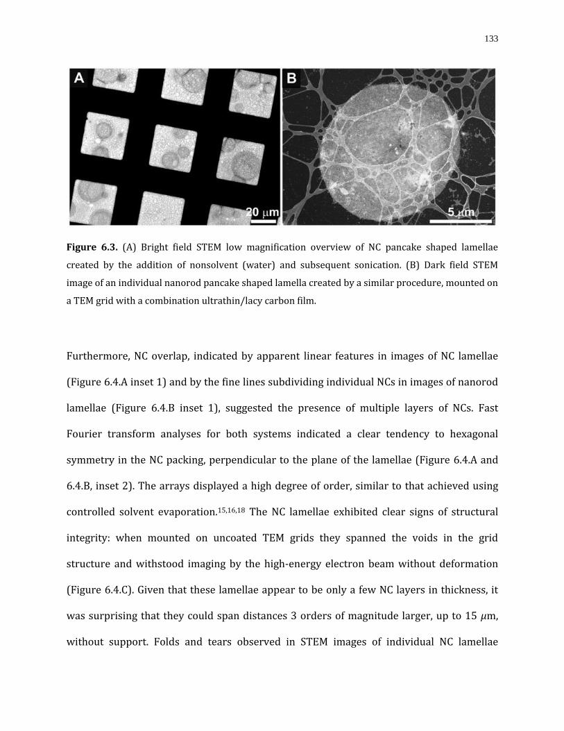
133
Figure 6.3. (A) Bright field STEM low magnification overview of NC pancake shaped lamellae
created by the addition of nonsolvent (water) and subsequent sonication. (B) Dark field STEM
image of an individual nanorod pancake shaped lamella created by a similar procedure, mounted on
a TEM grid with a combination ultrathin/lacy carbon film.
Furthermore, NC overlap, indicated by apparent linear features in images of NC lamellae
(Figure 6.4.A inset 1) and by the fine lines subdividing individual NCs in images of nanorod
lamellae (Figure 6.4.B inset 1), suggested the presence of multiple layers of NCs. Fast
Fourier transform analyses for both systems indicated a clear tendency to hexagonal
symmetry in the NC packing, perpendicular to the plane of the lamellae (Figure 6.4.A and
6.4.B, inset 2). The arrays displayed a high degree of order, similar to that achieved using
controlled solvent evaporation.15,16,18 The NC lamellae exhibited clear signs of structural
integrity: when mounted on uncoated TEM grids they spanned the voids in the grid
structure and withstood imaging by the high-energy electron beam without deformation
(Figure 6.4.C). Given that these lamellae appear to be only a few NC layers in thickness, it
was surprising that they could span distances 3 orders of magnitude larger, up to 15 μm,
without support. Folds and tears observed in STEM images of individual NC lamellae
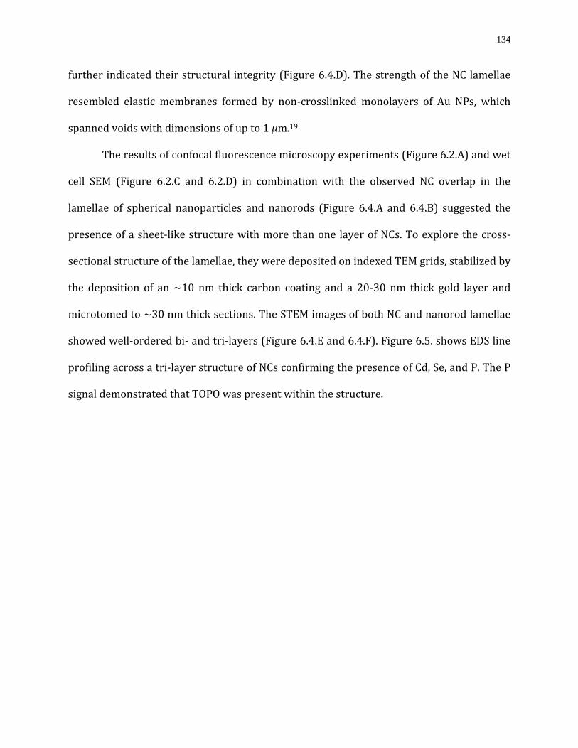
134
further indicated their structural integrity (Figure 6.4.D). The strength of the NC lamellae
resembled elastic membranes formed by non-crosslinked monolayers of Au NPs, which
spanned voids with dimensions of up to 1 μm.19
The results of confocal fluorescence microscopy experiments (Figure 6.2.A) and wet
cell SEM (Figure 6.2.C and 6.2.D) in combination with the observed NC overlap in the
lamellae of spherical nanoparticles and nanorods (Figure 6.4.A and 6.4.B) suggested the
presence of a sheet-like structure with more than one layer of NCs. To explore the cross-
sectional structure of the lamellae, they were deposited on indexed TEM grids, stabilized by
the deposition of an ∼10 nm thick carbon coating and a 20-30 nm thick gold layer and
microtomed to ∼30 nm thick sections. The STEM images of both NC and nanorod lamellae
showed well-ordered bi- and tri-layers (Figure 6.4.E and 6.4.F). Figure 6.5. shows EDS line
profiling across a tri-layer structure of NCs confirming the presence of Cd, Se, and P. The P
signal demonstrated that TOPO was present within the structure.
135
Figure 6.4. (A) STEM image of a NC lamella. Inset 1 shows NC ovelap indicated by linear structures.
Fourier transform (inset 2) indicates hexagonal symmetry. (B) STEM image of a nanorod lamella
inset 1 shows nanorod ovelap indicated by fine lines subdividing individual NCs. A region of
ordered hexagonal packing is confirmed by Fourier transform (inset 2). (C) SEM image of a lamella
(see 1) mounted on an uncoated Cu TEM grid. The lamella (∼15nm thick) spans the dark void (∼15
μm) (see 2) in the grid without support. (D) Examples of folds and tears present in lamellae
indicating their structural integrity. (E and F) Cross-sectional STEM images of NC tri- and bilayers.

136
For all cross sections, the thickness is ∼30 nm. The capping Au overlayer is used as a location
marker.
Figure 6.5. EDS line scan of a cross-sectioned QD lamellar tri-layer. A line scan showing the
presence of Cd (solid line), Se (dot dot dash) and P (dot dash). Ti (dot), which has no spectral
overlap with the elements of interest, is included as a background control. Cd, Se and P are all
significantly above background. Coincidence of P with Cd and Se indicates the presence of TOPO.
6.2.3. Proposed Mechanism of Lamellae formation To reconcile the plan view and the cross-sectional structure of the NC lamellae
(Figure 6.4.A and Figure 6.4.E, F, respectively) we propose the following interpretation of
our results. For a NC bilayer in plan view, projections of individual NCs are observed in a
hexagonal arrangement, surrounded by linear structures that follow the same symmetry
(Figure 6.4.A). These discrete, “individual” NC projections correspond to two NCs with
vertical alignment with AA-type layer stacking, whereas the linear structures are likely the

137
result of AB-type layer stacking. Supporting this observation, cross-sectional images
(Figure 6.4.E, F) show both regions of discrete single NC alignment along with extensive
regions of NC overlap. While it is also possible that coverage in the second layer is
incomplete, and NCs lie at the 2-fold sites, instead of the normal 3-fold sites for hard sphere
stacking, the cross section STEM images of lamellae argue against this since they show
extensive areas of continuous multilayers of NCs.
The NC center-to-center spacing of ∼6.5 nm in the plane of the lamellae was similar
to that observed for control samples (CdSe NCs deposited from toluene solution onto
carbon coated TEM grids and assembled via evaporation). However, the NC-to-NC spacing
between the layers was only ca. 4.5 nm (Figure 6.4.E and 6.4.F). We conjecture that water
may play a role in the preferential vertical compression between NC layers by inducing
asymmetries in either ligand distribution or conformation, driven by hydrophobic effects.
In either case, the reduction in interlayer distance between adjacent NCs is likely to
increase their dipole interactions.12,18 This may be an important factor in explaining the
structural integrity of these lamellae (the ground state dipole in the crystal is ∼100 D).20
We note that even if dipole-dipole interactions and hydrophobic forces between the QDs
are sufficient to stabilize the lamellae, the question of the driving force for their formation
remains. Assembly of QDs at the surface of aqueous droplets, driven by the reduction of
interfacial energy,14,21 occurred at short (<10 s) sonication times. It is likely that these
droplets served as precursors to the lamellar structures formed at longer sonication times
(15-30 s). We propose that exposure to ultrasound plays a key role by generating a
mechanical force in the system. Acoustic cavitation, a major effect of low frequency
sonication, induces high magnitude shear around oscillating bubbles.22,23 It has been

138
demonstrated that shear forces tend to elongate and stretch the emulsion droplets (while
surface tension forces try to oppose this effect).24 We conjecture that, with sufficient
elongation, the opposing walls of a droplet are brought into sufficiently close proximity that
dipole-dipole and hydrophobic forces acting between the QDs stabilize the resulting 2D
lamellar structure. From a broader perspective, at both the molecular and supramolecular
level, acoustic cavitation effects are gaining attention as a new route to the production of
novel architectures that cannot be obtained otherwise.25-28
6.2.4. Testing the Hypothesis and its Potential Applications
If, in the course of formation of the lamellae, water is confined between the NC
sheets, then not only is this important for the formation of the structure of the lamellae but
it also offers an opportunity to incorporate, in the “envelopes”, a wide variety of water-
soluble species. To test this hypothesis, we prepared NC lamellae in the presence of the
water-soluble dye, fluorescein isothiocyanate (FITC). Liquid state confocal fluorescence
microscopy showed matching localization of photoluminescence (PL) from FITC and CdSe
in the NC lamellae (Figure 6.6.A). To build from this observation and exploit its
implications, we incorporated a variety of water-soluble ionic, molecular, nanocrystalline
and biomolecular species into CdSe NC lamellae. EDS line scans across individual lamellae
showed that cobalt (Figure 6.6.B) introduced as salts in H2O (10 % v/v), were strongly
partitioned within the NC lamellae. Furthermore, EDS line scans of cross sections of
lamellae prepared with Co salts confirmed the presence of Co within the lamellar structure
(Figure 6.6.C). The incorporation of larger molecules into the lamellae interior was
demonstrated for water-soluble tris (2,2′-bipyridyl)ruthenium(II) (results not shown) and
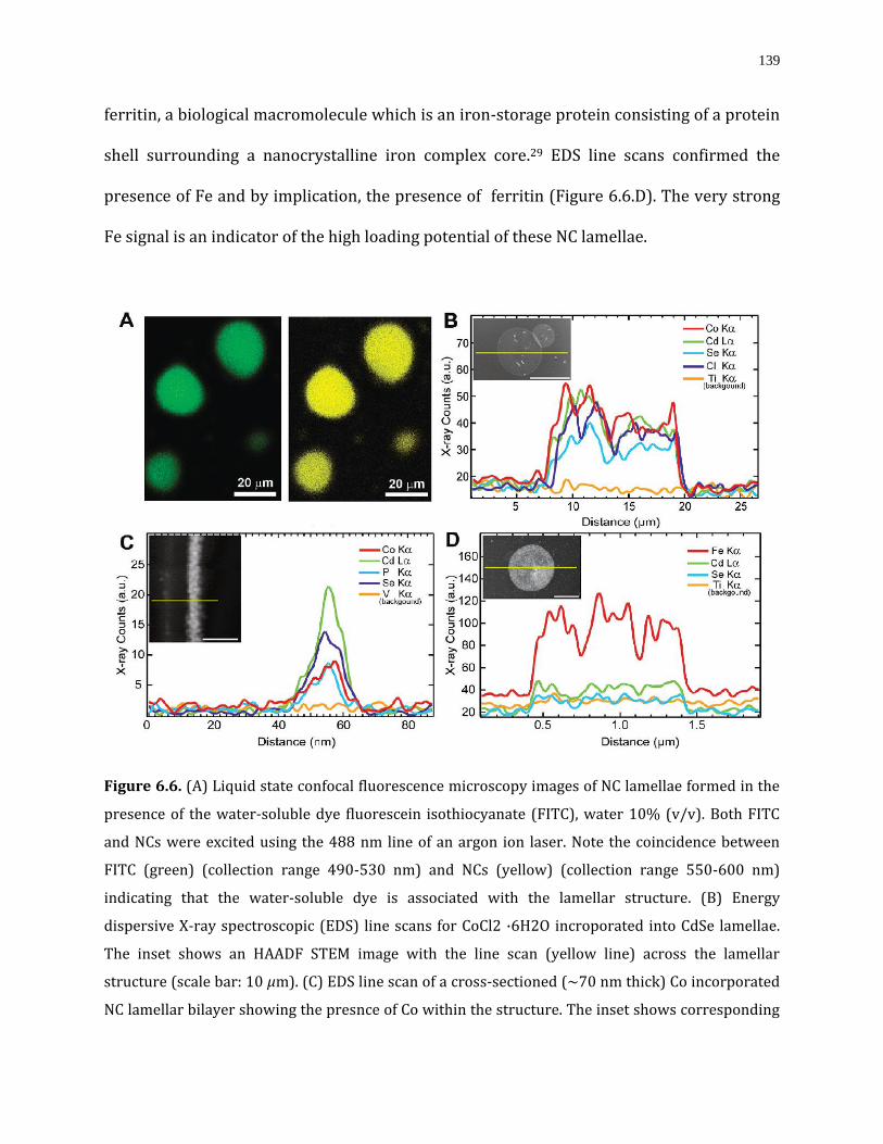
139
ferritin, a biological macromolecule which is an iron-storage protein consisting of a protein
shell surrounding a nanocrystalline iron complex core.29 EDS line scans confirmed the
presence of Fe and by implication, the presence of ferritin (Figure 6.6.D). The very strong
Fe signal is an indicator of the high loading potential of these NC lamellae.
Figure 6.6. (A) Liquid state confocal fluorescence microscopy images of NC lamellae formed in the
presence of the water-soluble dye fluorescein isothiocyanate (FITC), water 10% (v/v). Both FITC
and NCs were excited using the 488 nm line of an argon ion laser. Note the coincidence between
FITC (green) (collection range 490-530 nm) and NCs (yellow) (collection range 550-600 nm)
indicating that the water-soluble dye is associated with the lamellar structure. (B) Energy
dispersive X-ray spectroscopic (EDS) line scans for CoCl2 ·6H2O incroporated into CdSe lamellae.
The inset shows an HAADF STEM image with the line scan (yellow line) across the lamellar
structure (scale bar: 10 μm). (C) EDS line scan of a cross-sectioned (∼70 nm thick) Co incorporated
NC lamellar bilayer showing the presnce of Co within the structure. The inset shows corresponding

140
HAADF STEM image (scale bar: 35 nm). (D)EDS data for ferritin incorporated into the lamellae. The
inset shows a corresponding HAADF STEM image (scale bar: 500 nm). Note: Ti Kα or V Kα lines
were used as backgrounds since they have no spectral overlap with the elements of interest.
As a specific example of the potential functionality of CdSe NC lamellae, water
soluble citrate-capped Au spheroidal nanoparticles (NPs) with a mean diameter of 10 nm
were incorporated. Consistent with the other water-soluble species studied, the Au NPs
were found exclusively within the lamellae (Figure 6.8.A). EDS mapping showed the
uniform distribution of Cd and Se and well dispersed discrete Au signals indicating the
presence of Au NPs (Figure 6.7).
Figure 6.7. (A to D) EDS maps of Cd, Se, Au and Ti (background) respectively, corresponding to the
structure presented in Figure 6.8.A showing that distribution of Au NPs is fully contained within the
structure.

141
Two approaches were taken to confirm the internalization of the Au NPs. First, cross
sectional STEM imaging (Figure 6.8.B) showed the presence of Au NPs within the lamellar
structure. Second, simultaneous high resolution surface (SEM) and transmitted (TEM)
images of the same lamellar region were recorded. These results indicated that the Au NPs
were encapsulated (Figure 6.8.C and 6.8.D), in contrast to the control experiment (Figure
6.8.E) where Au NPs were added after lamellar formation and clearly present on the
surface. When semiconductor NCs are coupled with metal NPs, plasmon-exciton
interactions result in either enhancement or quenching of NC photoluminescence.30,31
Enhancement of emission occurs due to the plasmon-induced field enhancement effect,
whereas quenching of NC emission is due to energy transfer from NC to metal NPs.32,33 This
plasmon-exciton coupling interaction is of both practical and theoretical interest in the
research areas of light emitting devices, nanoscale lasing, and solar cells etc. To study the
effects of encapsulation of Au NPs on the luminescence of CdSe lamellae,
photoluminescence (PL) spectra were measured using confocal fluorescence microscopy
for 10 randomly selected lamellae with compartmentalized Au NPs. Lamellae formed by
CdSe NCs only were used in control experiments. Representative confocal fluorescence
microscopy images of control and Au NP encapsulated CdSe lamellae are presented in
Figure 6.8.G and 6.8.H, respectively. To compare the relative PL yield from each of these
structures, we plotted two histograms of the integrated PL intensity. Figure 6.8.F shows a
near doubling of the PL intensity for the Au encapsulated lamellae as compared to the
control sample. This PL enhancement is likely due to electronic interactions between the
Au NPs and the CdSe NCs in the “hybrid” lamellae.34 This interaction could result from
plasmonic enhancement of the NC radiative rate,35 or NC PL could be sensitized by

142
resonance energy transfer from Au NPs.36 A slight blue shift of PL maximum (582 to 574
nm) was detected similar to that observed in previous studies.37,38 In keeping with the
argument of Lee et al.,37 the blue shift may arise due to decreased exciton diffusion length
as a result of the increased radiative decay rate caused by exciton-plasmon interactions. To
further optimize luminescence enhancement of the lamellar structure, control of
experimental parameters, e.g., the type of encapsulated NPs, choice of QDs, their
concentrations, shape, dimensions, and variation of interparticle distances will be
required.32,33,39-41

143
Figure 6.8. (A) Incorporation of Au NPs into CdSe NC lamellae. In the HAADF STEM image shown,
the bright “dots” are individual Au NPs. (B) Crosssectional (∼30 nm thickness) STEM image
confirming the encapsulation of Au NPs inside the NC bilayer (as previously, an evaporated Au
layer, upper portion of the image, is used as a marker). (C and D) Simultaneously recorded SEM and
TEM images, respectively, confirming encapsualtion of Au NPs within the NC lamellae. (E) SEM
image of control sample with Au NPs added after the NC lamellae formation. (F) Histogram showing
10 maximum photoluminescense intensity measurements for both NC lamellae and Au
encapsulated NC lamellae. (G and H) Representative fluorescence confocal microscope images of
CdSe NC lamellae and Au encapsulated NC lamellae, respectively.

144
6.3. Summary and Conclusions
This study demonstrates a facile, solution-based, method that involves controlled
addition of a nonsolvent (water) combined with sonication to trigger the formation of
micrometer-size lamellar sheets of ordered NC arrays. The most striking characteristics of
these structures are that, while they are many micrometers in diameter, they are typically
only two or three NC layers in thickness (∼15 nm), yet they exhibit structural integrity
without recourse to chemical cross-linking. In addition, the properties of the lamellar
structures can be modified by internalizing water soluble species including but not limited
to ionic salts, metal nanoparticles (NPs), and biomolecular complexes. The possibility of
tuning the optical properties of the NC lamellae was demonstrated by enhancing PL
intensity via incorporation of Au NPs. We speculate that these ions or molecular complexes
may be useful in photoelectrochemical processes, e.g., in forming redox couples in an
ordered, nanoparticle solar cell.42-44 More fundamentally, these structures mark a step
toward ordered, compartmentalized, NC-based synthetic complexes whose properties can
be modulated by the cargo they carry.

145
References
(1) Whitesides, G. M.; Boncheva, M. Proc. Natal. Acad. Sci. U.S.A. 2002, 99, 4769–4774.
(2) Whitesides, G. M.; Grzybowski, B. Science 2002, 295, 2418–2421.
(3) Antonietti, M.; Goltner, C. Angew. Chem., Int. Ed. Engl. 1997, 36,910–928.
(4) Hamley, I. W. Angew. Chem., Int. Ed. 2003, 42, 1692–1712.
(5) Ozin, G. A. AdV. Mater. 1992, 4, 612–649.
(6) Philp, D.; Stoddart, J. F. Angew. Chem., Int. Ed. Engl. 1996, 35, 1155–1196.
(7) Glotzer, S. C.; Solomon, M. J. Nat. Mater. 2007, 6, 557–562.
(8) Alivisatos, A. P. Science 1996, 271, 933–937.
(9) Weller, H. Angew. Chem., Int. Ed. Engl. 1996, 35, 1079–1081.
(10) Scholes, G. D.; Rumbles, G. Nat. Mater. 2006, 5, 683–696.
(11) Rogach, A. L.; Talapin, D. V.; Shevchenko, E. V.; Kornowski, A.;Haase, M.; Weller, H.
Adv.Func. Mater. 2002, 12, 653–664.
(12) Tang, Z. Y.; Zhang, Z. L.; Wang, Y.; Glotzer, S. C.; Kotov, N. A.Science 2006, 314, 274–278.
(13) Boker, A.; He, J.; Emrick, T.; Russell, T. P. Soft Matter 2007, 3, 1231–1248.
(14) Lin, Y.; Skaff, H.; Emrick, T.; Dinsmore, A. D.; Russell, T. P. Science2003, 299, 226–229.
(15) Murray, C. B.; Kagan, C. R.; Bawendi, M. G. Science 1995, 270,1335–1338.
(16) Shevchenko, E. V.; Talapin, D. V.; Kotov, N. A.; O’Brien, S.; Murray,C. B. Nature 2006,
439, 55–59.
(17) Lasic, D. D. Liposomes from physics to applications; Elsevier: 1993.
(18) Talapin, D. V.; Shevchenko, E. V.; Murray, C. B.; Titov, A. V.; Kral, P. Nano Lett. 2007, 7,
1213–1219.

146
(19) Mueggenburg, K. E.; Lin, X. M.; Goldsmith, R. H.; Jaeger, H. M.Nat. Mater. 2007, 6, 656–
660.
(20) Shim, M.; Guyot-Sionnest, P. J. Chem. Phys. 1999, 111, 6955–6964.
(21) Lin, Y.; Skaff, H.; Boker, A.; Dinsmore, A. D.; Emrick, T.; Russell,T. P. J. Am. Chem. Soc.
2003, 125, 12690–12691.
(22) Elder, S. A. J. Acoust. Soc. Am. 1959, 31, 54–64.
(23) Richardson, E. S.; Pitt, W. G.; Woodbury, D. J. Biophys. J. 2007, 93,4100–4107.
(24) Cristini, V.; Guido, S.; Alfani, A.; Blawzdziewicz, J.; Loewenberg, M. J. Rheol. 2003, 47,
1283–1298.
(25) Bardelang, D. Soft Matter 2009, 5, 1969-1971.
(26) Paulusse, J. M. J.; Sijbesma, R. P. Angew. Chem., Int. Ed. 2006, 45,2334–2337.
(27) Bardelang, D.; Camerel, F.; Margeson, J. C.; Leek, D. M.; Schmutz,M.; Zaman, M. B.; Yu,
K.; Soldatov, D. V.; Ziessel, R.; Ratcliffe, C. I.; Ripmeester, J. A. J. Am. Chem. Soc. 2008, 130,
3313-3315.
(28) Hickenboth, C. R.; Moore, J. S.; White, S. R.; Sottos, N. R.; Baudry, J.; Wilson, S. R. Nature
2007, 446, 423–427.
(29) Lawson, D. M.; Artymiuk, P. J.; Yewdall, S. J.; Smith, J. M. A.; Livingstone, J. C.; Treffry, A.;
Luzzago, A.; Levi, S.; Arosio, P.; Cesareni, G.; Thomas, C. D.; Shaw, W. V.; Harrison, P. M.
Nature 1991, 349, 541–544.
(30) Shimizu, K. T.; Woo, W. K.; Fisher, B. R.; Eisler, H. J.; Bawendi, M. G. Phys. Rev. Lett.
2002, 89, 117401.
(31) Hosoki, K.; Tayagaki, T.; Yamamoto, S.; Matsuda, K.; Kanemitsu, Y. Phys. Rev. Lett. 2008,
100, 207404.

147
(32) Govorov, A. O.; Bryant, G. W.; Zhang, W.; Skeini, T.; Lee, J.; Kotov,N. A.; Slocik, J. M.; Naik,
R. R. Nano Lett. 2006, 6, 984–994.
(33) Govorov, A. O.; Lee, J.; Kotov, N. A. Phys. Rev. B 2007, 76, 125308.
(34) Barnes, W. L. J. Mod. Opt. 1998, 45, 661–699.
(35) Chance, R. R.; Prock, A.; Silbey, R. Adv. Chem. Phys. 1978, 37, 1-65.
(36) Saini, S.; Shenoy, V. B.; Bagchi, B. J. Phys. Chem. C 2008, 112,6299–6306.
(37) Lee, J.; Govorov, A. O.; Dulka, J.; Kotov, N. A. Nano Lett. 2004, 4,2323–2330.
(38) Hsieh, Y. P.; Liang, C. T.; Chen, Y. F.; Lai, C. W.; Chou, P. T. Nanotech. 2007, 18, 415707
(39) Kulakovich, O.; Strekal, N.; Yaroshevich, A.; Maskevich, S.; Gaponenko, S.; Nabiev, I.;
Woggon, U.; Artemyev, M. Nano Lett. 2002, 2, 1449–1452.
(40) Chen, C. W.; Wang, C. H.; Wei, C. M.; Chen, Y. F. Appl. Phys. Lett. 2009, 94, 071906.
(41) Pompa, P. P.; Martiradonna, L.; Della Torre, A.; Della Sala, F.; Manna, L.; De Vittorio, M.;
Calabi, F.; Cingolani, R.; Rinaldi, R. Nat. Nanotech. 2006, 1, 126–130.
(42) Gratzel, M. Nature 2001, 414, 338–344.
(43) Hagfeldt, A.; Gratzel, M. Chem. ReV. 1995, 95, 49–68.
(44) Kamat, P. V. J. Phys. Chem. C 2008, 112, 18737–18753.

148
Chapter 7
Towards an Experimental Demonstration
of ‘2D’ Visible Range Cloaking via a
Bottom-up Approach
This chapter explores a bottom-up method to produce a metamaterial which can
potentially function as an optical cloak in the visible range. A composite material
consisting of an array of silver nanowires (NWs) in a dielectric host has been produced
based on the theory of a non-magnetic optical cloak.1 The required radial array of silver
NWs was achieved by electroless deposition of the metal into the channels of a porous
alumina structure grown perpendicularly from the curved surface of a micrometer scale
aluminum wire. While the required architecture and dimensions may require further
adjustment, the functionality of the cloak in the visible range has been demonstrated.
Fundamentally this metamaterial structure represents an important step forward in the
production of tunable, optically functional, complex three dimensional architectures
through the bottom-up approach.

149
7.1. Introduction
7.1.1. Metamaterials and Optical Cloaking via Transformation
Optics
Metamaterials are artificially constructed composite materials which exhibit
ensemble electromagnetic (EM) properties not present in the constituent materials.2-8 The
heterogeneity of these materials exists on a length scale smaller than the wavelength of
interest. Thus, the EM response of the material is a function of the collective behavior of a
material’s components (an overview of metamaterials is provided in Chapter 1).
As a consequence of their tunable EM properties, metamaterials have become a
focus in the area of transformation optics.4,7,9-12 Transformation optics explores the control
of light paths via manipulation of the spatial distribution of permittivity (ε) and
permeability (μ)13 within metamaterials. In effect, transformation optics7,12 describes the
conditions necessary to ‘warp’ light space in a manner analogous to warping space-time in
general relativity.
Within the realm of transformation optics, the possibility of optical cloaking (i.e.,
invisibility) has sparked scientific curiosity in recent years.1,14-19 In a perfect optical cloak,
the object to be rendered invisible will create no reflection, scattering or absorption.
Figure 7.1 illustrates an optical cloak in a spherical coordinate system where light is bent
around an object and redirected to its original trajectory. The object being cloaked is to be
placed within the inner sphere whereas the region between the inner and outer sphere
constitutes the cloaking device.

150
Figure 7.1. Schematic illustration of a three-dimensional view showing the wave trajectories of a
spherical cloaking system. Reprinted with permission from Reference 14. Copyright 2006, Science.
In any naturally occurring material, light rays will bend toward the center of the
sphere due to the material’s higher refractive index in accordance with Snell’s law.20 To
diffract light rays away from the center, a material whose refractive index is less than 1 is
required. For example, one way to achieve this is by employing thin metallic wires in a
dielectric host which acts to ‘dilute’ the metal and thus reduce the plasma frequency to
obtain ε less then unity, for a desired wavelength.21
One exploitation of this notion, is the design of an optical cloak which was
introduced by Pendry18 and Leonhardt et al.7,18 In this model, the path of the EM wave was
controlled by using a specific spatial profile of ε and μ to make light avoid a particular
region in space. Figure 7.2 shows an example of the transformed media using ε and μ
tensors. In a homogenous medium where ε and μ are constant, a straight field line is
produced. However, by varying the spatial distribution of ε and μ, a distorted field line
results as it travels through the heterogeneous medium.

151
Figure 7.2. (A) Straight field line through a homogeneous medium against a Cartesian coordinate
system (B) distorted field line travelling through a heterogeneous medium produced by varying the
spatial distribution of permittivity and permeability. Reprinted with permission from Reference
14. Copyright 2006, Science.
For the design of an optical cloak, in the case of a cylindrical coordinate system, the region
0 < r < b is transformed into < r’ < b by using the following transformation:
( )
where a and b are the radius of the core (i.e., region of invisibility) and the distance from
the center of the core to the outer diameter (i.e., perimeter of the cloak) respectively. r and
r’ are the radial coordinates in the original and transformed system respectively z’ and θ’
are the coordinates of the transformed system respectively.
The transformed region extends from a to b only, shown in Figure 7.3. The
transformation can be obtained by the following space profiles of ε and μ for the case of a z-
polarized incident field:
(
)
(
)
( )

152
It should be noted that only has a gradient as a function of radius and thus this type of
transformation is known as a magnetic cloak. However, this type of transformation still
suffers from non-zero scattering. The first practical demonstration of a cloak based on the
above mentioned transformation was performed by Schurig et al at microwave frequencies
in 2006.19
Figure 7.3. A two-dimensional cross-sectional view of wave trajectories of a spherical cloaking
system where light is deviated around the object to be cloaked (radius a) within the annular cloak
region (radius b – a) and return to its original path. Reprinted with permission from Reference 14.
Copyright 2006, Science.
7.1.2. Theoretical Design of a Non-magnetic Optical Cloak
The magnetic cloak discussed above cannot be practically scaled down in
dimensions for the development of a cloak in the visible spectrum range as indicated by
Klein et al.22 An alternative theoretical solution for a non-magnetic cloak which can operate
at optical frequencies (390 to 750 nm) was proposed by Cai and Shalaev et al.1 Our bottom-
up approach for the production of the cloaking structure illustrated in the following
sections is based on this model. In the model, ε has a gradient as a function of radius. Figure
7.4 illustrates a coordinate transformation of this cylindrical shell model. The proposed

153
design should meet the following space profile for transverse magnetic (TM) illumination
(i.e., the magnetic field polarized along the z-axis):
(
)
(
)
(
)
( )
where , and are the azimuthal and the radial dielectric permittivity and the z-axis
magnetic permeability respectively.
Figure 7.4. The coordinate transformation of a cylindrical shell model. A cylindrical region r<b into
a concentric cylindrical shell a <r < b. There is no variation along the z direction. Reprinted with
permission from Reference 13. Copyright 2007, Nature.
It should be pointed out that although this design can produce the desired trajectory of
light, impedance mismatch at the outer boundary of the cloak occurs. This results in a
certain amount of scattering determined by the ratio of a to b. The main advantage of this
theoretical design is its ease of fabrication due to the fact that no magnetic resonance is
required. Further is a constant and is larger than unity which can be easily achieved
through a variety of dielectric materials. The largest design challenge is the choice and
control of an appropriate metamaterial where the profile of varies from 1 to 0 as the
wave propagates from the outer boundary of the cloak b to the inner a.

154
The space profile of εr and εθ dictates an interaction between the media and applied
field in the radial direction only, whereas negligible interaction in the azimuthal direction is
desirable to provide a constant εθ. The choice of metallic rod-like structures (e.g., arrays of
nanowires or nanoparticles) is well-suited for this purpose since it lends itself to predictive
modeling via the effective medium theory.23,24
Let us consider a metal ellipsoid with three perpendicular semiaxes ai (i=1,2,3). The
depolarization factor q1 for incident field polarized along a1 is given as:
∫
( ) (
) ( )
( )
Similar expressions for q2 and q3 can be obtained with cyclic changes. In the case of a long
elliptical cylinder, a2=a3 and a1 >> a2 which will result in q1≈0 and as q1+q2+q3=1, therefore
q2=q3=0.5. The screening factor k which indicates the strength of interaction between the
wire and the applied field is given by:
( )
(7.5)
Equation (7.5) shows that k1 will achieve a very large value whereas k2= k3=1. Therefore, if
the long axis of the metal nanowires or rods (i.e., a1) is in the radial direction, we will
observe a strong interaction in the radial direction whereas the interaction in the
transverse direction will be negligible. The effective permittivity of such a composite media
in a given direction is:
[ ̅ √ ̅ ] ( )

155
where ̅ [( ) ] [ ( ) ] . As we expect no interaction in the
azimuthal direction:
(
)
( )
where is the permittivity of the dielectric host. Thus the ratio of inner to outer radius of
the cloak (R=a/b) is governed by :
( )
where and are the filling factors for the metal nanowires at the inner and outer
surfaces of the cloak respectively and their ratio should satisfy the above relation.
Considering the possible dimensions of the cylindrical shell i.e., a and b that can be
achieved by the bottom-up approach, we have utilized radial arrays of silver nanowires
(and nanoparticles). From a practical, experimental point of view, it is important to note
that as long as the Equations from (7.4) to (7.8) are satisfied, the key parameters i.e., a, b
and filling factors may be varied considerably. Given the complexity of the components
involved in generating the necessary architecture, such flexibility is critical in producing
the necessary structure. Based on these equations, examples of the design possibilities are
presented in Figure 7.5 which shows the calculated variation of r as a function of design
parameters e.g., a and b at the operating wavelength of 500 nm. For these examples, we
used silver nanowires (NWs) in a dielectric host, alumina (See Route III, Section 7.2.3). The
required variation of r from 0 to 1 for the interior and exterior surfaces of the cloak
respectively are achieved by a = 0.7 µm and b = 2 µm (Figure 7.5 A) and a = 1.2 µm and b =
3.5 µm (Figure 7.5 B). In order to satisfy the equations, the corresponding filling factors are

156
f0 =24.4 % and f1 =9.4 % and values of R calculated from Equation (7.8) is 0.35 at the
operating wavelength of 500 nm.
Figure 7.5. Calculated plot of radial component of electric permittivity (εradial) as a function of cloak
dimensions (A) a = 0.7 µm and b = 2 µm (B) a = 1.2 µm and b = 3.5µm. Both parameters result in
the effective permittivity at operating wavelength of 500 nm. Silver nanoparticles with a radius of
10 nm were used for the calculations.

157
7.2. Results and Discussions
7.2.1. Experimental Rationale
The model proposed by Cai and Shalaev et al1 represents a significant fabrication
challenge for both top-down and bottom-up approaches. Figure 7.6 and Table 7.1.
summarize the required parameters for the bottom-up approach of a ‘2D’ cloaking material
at a visible frequency. Based on this model the target dimensions for our experiment for
the object to be cloaked is approximately 1 µm in diameter surrounded by a cylindrical
cloak with a wall thickness of approximately 1.5 µm. In addition, the metamaterial cloak
consists of a radial array of metal NWs in an appropriate dielectric host. Since the
refractive index of the cloak is required to be 0 at the interior and 1 at the exterior, it is
critical that the filling factor of the metal within the dielectric host varies accordingly. For
example, if the specific cloak dimensions described above are used, a filling factor of metal
NWs (or a radial array of nanoparticles (NPs)) of 4% at the exterior and 12% at the interior
of the cloak is needed. While structures in this dimensional range are relatively simple to
achieve via top down methods, the most significant challenge is the formation of a radial
array of metal NWs organized within the dielectric host. The NWs are required to be less
than 1/10 in width of the incoming optical wavelength. For example, this would require a
NW width of less than approximately 40 nm for blue light and less than 70 nm for red light.
While the formation of metal NWs in this size range is possible using focused ion beam
technology,25 the device is required to be three-dimensional. Specifically, using top-down
strategies, only one layer could be deposited at a time and multiple individual layers of

158
dielectric and subsequent radial metal deposition would need to be manufactured. The
time and cost of this process rules it out as a practical approach.
Figure 7. 6. Schematic illustration of the non-magnetic cloak structure. Inner core (dark grey) is the
cloak area surrounded by metal nanowires (NWs) in a dielectric host. A Radial array of NWs is
perpendicular to the z-axis and must satisfy the filling factor such that the radial component of
electric permittivity varies from 0 at a to 1 at the exterior surface. Spatial positions of NWs do not
need to be periodic.
Table. 7.1. Summary of required parameters for the fabrication of a non-magnetic optical cloak
device.
Material Arrays of metal nanowires or nanoparticles (eg, gold or silver)
Host for metal Dielectric (e.g., SiO2, Al2O3) Shape of host Cylindrical Metal orientation Radial Metal width 40-70 nm or less Filling factors of metal Must satisfy εrad 0 at inner boundary to εrad = 1 at outer
boundary. The filling factor varies depending on dimensions of host and metal (eg, for a = 1.4 µm, b = 4 µm and metal width ~10 nm, f0=18.6% and f1 =6.6%).
Additional practical notes (1) Diameter of object to be cloaked is ~ 30% of total diameter of cloaking device.

159
(2) Variations in metal length may not be important as long as filling factor is satisfied (i.e.,averaging effect). (3) System must be robust, processible, temporally stable and needs to be responsive and allow for fine tuning.
Using a bottom-up approach, the general rationale would be to produce a NW (or
NP) array which is stabilized by a dielectric host. A porous dielectric host with tunable
dimensions can be realized and subsequently, the pores can be populated with appropriate
metal NWs (See details in Section 7.2.3, Route III).
Figure 7.7 is a summary of three possible routes which were explored for the
fabrication of the optical cloak via bottom-up approaches.
Figure 7. 7. Summary of explored routes for the fabrication of a non-magnetic optical cloak device.

160
7.2.2. Routes I and II
Of the three approaches outlined in Figure 7.7, Route III (Section 7.2.3) allowed for the
production of structures falling within the range of the desired parameters while Route I
and II, failed to produce effective architectures. The preliminary experimental data for
Routes I and II (Figure 7.8) will be discussed concisely in this section.
Figure 7.8. Schematic showing two possible routes to produce the optical cloak. Route I: vertical
assembly of gold nanorods on silica then subsequently embedded via silica deposition. Route II:
radial assembly of binary metal NWs (eg, gold/nickel) around a cylindrical host directed by a
controlled magnetic field.

161
In preliminary experiments via Route I, the concept is to produce a radial array of
NWs or NRs which project vertically from the surface of dielectric spheres with subsequent
‘embedding’ of the NWs through the deposition of an additional layer of dielectric. By
repeating this process in a stepwise manner, multiple layers of radially arranged NWs in a
dielectric host could be produced. The vertical assembly of NWs can be realized, in
principle, by functionalizing their ends. However, one of the foreseen challenges of this
approach is that since both ends of the NWs are functionalized, there is the possibility of
undesired ‘bridging’ of adjacent spheres by NWs or attachment of both ends of a single NW
to the substrate.
Silica spheres (and hollow silica spheres)26 were chosen as the dielectric host and
substrate for assembling metal NW arrays. Monodisperse colloidal silica (SiO2) particles
were prepared by controlled hydrolysis and condensation of tetraethylorthosilicate (TEOS)
in ethanol to which water and ammonia were added (the Stöber method).27 We produced
highly monodisperse spherical SiO2 particles with dimensions ranging from 300 to 500 nm.
Gold nanorods (NRs) (L NRs = 40 ± 4 nm, H NRs= 13 ± 1 nm) were synthesized and the ends of
NRs were functionalized with 3-mercaptopropyl trimethoxysilane to facilitate their vertical
assembly on the surface of the SiO2 spheres. Figure 7.9 shows the results of vertical gold
NR assembly on the silica particles. Although the majority of NRs observed were close to
vertical alignment, the number density of NRs on the surface of the spheres was
consistently too low to move on to the next step of multiple layer formation. In addition,
direct ‘seed’ deposition of gold on the surface of SiO2 particles was explored. In this
approach, gold seed nanoparticles were obtained by the reduction of HAuCl4 by NaBH4.
These seeds were then deposited and grown on the surface of the SiO2 spheres. In both

162
cases, the required control of NR vertical assembly necessary for this hybrid structure to be
effective as a cloak was not achieved.
Figure 7.9. Representative TEM image of vertical assembly of gold nanorods onto synthesized silica
particles. The ends of gold nanorods were functionalized by the introduction of 3-mercaptopropyl
trimethoxysilane.
As an alternate approach (Route II) an attempt was made to create a radial array of
nickel-tipped gold NWs by the use of a magnetic field in an “anti-Helmholtz” configuration.
Figure 7.10 illustrates an electrochemical method28-30 for the production of binary NW
structures consisting of gold and magnetically responsive nickel. A thin film of silver (~400
nm) was evaporated on a commercially available aluminum oxide filter (AnodiscTM, USA)
and used as the cathode. A platinum wire served as an anode. A silver “buffer layer” was
deposited first to fill the pores evenly, followed by gold and nickel deposition. The
optimized plating conditions were 0.5 mA/cm2 for deposition times of 10 to 60 min,
depending on the desired length of each segment. Figure 7.10 shows examples of

163
representative SEM images of the resultant binary structures with varying lengths. Energy
dispersive X-Ray spectroscopy (EDS) mapping confirms the composition.
Figure 7.10. Schematic illustration of the electrochemical method used to produce binary
nanowires (NWs) composed of nickel and gold.

164
Figure 7.11. (A) Backscattered SEM images of binary NWs showing various lengths of each
component. Note: silver is used to fill the bifurcated pores to provide even deposition of gold and
nickel (B) EDS mapping showing atomic composition of NWs.
For the magnetic radial assembly, as synthesized binary Ni-Au NWs described above
were used as a building-block. Figure 7.12 (A) shows the simulation of the magnetic field
lines analogous to the Helmholtz configuration. In this configuration, the opposing poles of
cylindrical annular magnets are facing each other such that a homogenous magnetic field
can be produced within the central region between the magnets. However, when their
dipole moments are aligned in the anti-Helmholtz configuration i.e., the same poles are
facing each other, the magnetic fields from two poles flow in opposite directions. This

165
results in a zero net magnetic field at the center surrounded by a radial field as indicated in
Figure 7.12 (B).
Figure 7.12. Magnetic field line simulations analogous to (A) Helmholtz and (B) anti-Helmholtz
configurations.
By exploiting the anti-Helmholtz configuration, we hypothesized that radial
assembly of the binary NWs could be achieved in this region where the radial magnetic
field lines are compressed along the horizontal axis between two magnets due to the
resulting pressure in the field by repulsion. Figure 7.13 (A) shows a photograph of our
general experimental set-up. Annular magnets were arranged in an anti-Helmholtz
configuration and placed on a capillary tube (or a glass vial) containing binary NWs in an
aqueous solution. This set-up should produce a radial magnetic field line in the central

166
zone between the magnets such that the magnetically responsive component, Ni, of the
binary NWs should align within this field. Figure 7.13 (B) shows the top-views of NW
assembly in the Helmholtz and anti-Helmholtz configurations respectively. In the case of
the Helmholtz configuration, most of the NWs were aligned parallel to the field and thus
from the top view, we are looking down the long axis of the NWs. For the anti-Helmholtz
configuration, a distinctly different radial distribution of NWs was observed. Although the
radial alignment of NWs was successful on the millimeter scale, there was insufficient
control once the process was miniaturized to the micrometer scale. Further, while radial
arrangement of NWs was possible, achieving precise radial control of the volume fraction
via magnetic fields was problematic.
Figure 7.13. (A) Example of experimental set-up using annular magnets in an anti-Helmholtz
arrangement producing a radial magnetic field in the central zone between magnets (B) Optical

167
micrographs showing top-views of NW assemblies via the two different configurations, showing a
radial alignment of NWs in the anti-Helmholtz arrangement.
7.2.3. Route III
7.2.3.1. Fabrication of a Cylindrical Shaped Dielectric Host
Our third approach (Route III) was to use a porous host as a template for creating
radial metal arrays. While the model proposed by Cai and Shalaev et al 1 (see section 7.1.2)
considers silica as a dielectric host and silver NWs, a combination of other dielectrics and
metals is possible. Of the available materials, porous alumina is particularly attractive since
the band gap energy of alumina (Al2O3) is approximately 9 eV and its critical wavelength
(see Chapter 1) at room temperature is approximately 0.14 µm which makes alumina
transparent in the visible range (note, band gap energy and critical wavelength of SiO2 ≃
8.5 eV and ≃ 0.15 µm respectively).31,32 Dimensions of porous alumina can be controlled by
the appropriate selection of applied voltage during anodization.33 Further, since the
starting material, aluminum, can be readily fabricated into wires with a diameter smaller
than 20 µm, this metal offers a unique opportunity for a structure to produce its own cloak.
Figure 7.14 is a schematic illustration of the method for the production of a radial porous
alumina template as a dielectric host for the optical cloak.

168
Figure 7.14. Schematic of the proposed route to the fabrication of radial porous alumina as a
dielectric host via anodization of aluminum (Al) wire. The cross-sectional view shows a metallic Al
core surrounded by a porous alumina coating with a radial distribution of pores.
Anodized aluminum oxide (AAO) is a material whose thickness, pore size and pore
volume fraction can be readily manipulated through chemistry and applied potential
during oxide growth.34-36 Porous AAO as a dielectric host should provide: (1) radial arrays
of pores for metal deposition and (2) appropriate pore size and template dimensions to
potentially satisfy the filling fraction of metal required by the theoretical model.1
In our work, the anodization process was carried out on an aluminum wire (Al,
99.999%, purchased from Alfa Aesar) electropolished to be less than 5 µm in diameter. An
Al wire should in principle, provide radial arrays of pores, since it is known that pores grow
perpendicular to the Al metal surface. This is because there is an equilibrium of oxide
dissolution and oxide growth at the interface between oxide/electrolyte and metal/oxide
respectively.37 The net reaction during anodization is:
169
2Al + 3H2O → Al2O3 +3H2
Oxide growth is electrochemically driven by the movement of oxygen containing ions (e.g.,
O2-/OH-) at the metal/oxide interface from the electrolyte through the oxide layer at the
bottom of the pore where the following reaction takes place:
2Al +3O2- → Al2O3 +6e-
By the hydration reaction, the dissolution of the oxide layer results. Al3+ ions migrate through
the oxide layer and eject into the electrolyte solution at the oxide/electrolyte interface.
This loss of Al3+ ions into the electrolyte is necessary for growth of the porous oxide:
Al2O3 +6H+→2Al3+ +3H2O
At the cathode, hydrogen gas evolution can occur by the ejection of electrons into the
electrolyte solution:
6H+ + 6e– → 3H2
This balance between the growth of Al2O3 and the loss of Al3+ ions, is key to producing
alumina’s porous columnar structure.37,38
We explored growth rate, pore density, pore regularity and overall integrity of the
oxide layer by using a number of acids e.g., sulfuric, phosphoric and oxalic acids33,34 to
determine optimal conditions for radial oxide growth. In the case of sulfuric acid (15 v %
in an aqueous solution at 10 °C), the AAO growth rate was rapid (>1 µm in 5 min) and it
produced a high pore volume fraction. Therefore, the commensurate pore diameter was
too small to satisfy the model.1 Phosphoric acid had a significantly slower growth yielding
controllable pore size but suffered from bifurcation, that is, branching during the
anodization process which suggested that control over pore volume by varying applied

170
potential would be impossible. Ultimately, oxalic acid (3 wt %, in aqueous solution at 21
°C), was chosen because it formed straight, well defined pores with dimensions in broad
compliance with those required by the model. Figure 7.15 shows representative SEM
images of the AAO host formed in the presence of oxalic acid. A cylindrical oxide shell was
grown with pores perpendicular to the Al wire surface. Relatively straight porous channels
without bifurcation were formed.
Figure 7.15. SEM images of (A) Bare Aluminum wire after electropolishing. (B) Anodized
aluminum oxide (AAO) grown as a cylindrical dielectric shell around an Al wire core. (C) Surface
morphology of AAO shell showing a uniform pore structure (D) A cross-sectional view of radial
porous AAO grown using 3 % Oxalic acid (nb, surface roughness shown is due to fracturing
artifact).

171
Although the theoretical model requires a filling factor for silver NWs of 12 % for
the interior and 4 % for the exterior of the cloak,1 for the dimensions and wavelength of a ≈
0.5 µm, b ≈ 2 µm and 633 nm respectively, the model affords significant flexibility. This is
because the required filling factor varies with the dimensions of the host and the object to
be cloaked. Therefore, we investigated the effect of oxide growth and subsequent pore
size, volume, and density by applying various potentials to the electrolyte.33 Assuming a 2D
dense packing of the pores, applied voltage dependent average pore size and cell size (that
is the distance between adjacent pores) were measured by analyzing SEM micrographs.
Figure 7.16 (A) shows the variations of average pore size and average cell size plotted as a
function of applied potential. In the voltage range 30 – 18 V, the AAO pore diameter
showed only a modest decrease while a significant decrease of the average cell size was
observed. This feature is critical in providing the template for the required filling factor
control.
Figure 7.16. (A) Variations of average pore diameter (blue circle) and average cell size (red
square) as a function of applied potential. (B) Calculated pore volume fraction as a function of

172
applied voltage. The oxide layer was electrochemically grown over 105 minutes using 3 wt. % of
Oxalic acid in water as an electrolyte solution.
Figure 7.16 (B) shows the variation in the pore volume fraction as a function of applied
voltage. The volume fraction was calculated as V = 78.5P2/C2 from the pore diameter (P)
and the cell size (C) based on the assumption that the cross-section of pores is cylindrical
and constant.33 As can been seen from Figure 7.16 (B), by choosing the appropriate applied
voltage, it is possible to alter the volume fraction of the pores from greater than 15 % to
less than 5 %. It is important to note that during the growth process of approximately 100
min the voltage has to be changed gradually to prevent bifurcation or the formation of
steps which could influence subsequent metal loading.
During preliminary studies with thicker wires of 10-15 µm in diameter, severe
cracking of the AAO was observed. The reason for cracking is unclear however based on
our observations, it appeared to be related to the thickness of the AAO layer. This may be
due to the fact that AAO occupies a measurably larger volume than the aluminum substrate
from which it grows. Since significant compressive stresses are induced during the growth
process36 these are likely exacerbated by the high radius of curvature of our cylindrical-
shaped system. However, as we approached the target dimensions required for cloaking
(e.g., a = 0.6 µm and b = 1.75 µm), cracking routinely terminated at a wire diameter of
approximately 5 µm, with an uninterrupted porous radial array below this diameter.

173
7.2.3.2. Electroless Deposition of Ag NPs and Ag NWs into AAO
pores
Initially, a pulsed electrochemical approach using silver nitrate (AgNO3) was
employed. However, it typically produced polydisperse silver NWs with incomplete pore
filling. Consequently, we focused on electroless deposition via polyol reduction of Ag+ ions.
In a typical polyol synthesis, ethylene glycol reduces AgNO3 to produce Ag atoms by the
following mechanism:39
2HOCH2CH2OH ⟶ 2CH3CHO + 2H2O
2Ag+ +2CH3CHO ⟶ CH3CO—OCCH3 + 2Ag +2H+
Similar to the synthesis of quantum dots, nucleation and growth of silver nanostructures
can be initiated once the concentration of silver atoms reaches the supersaturation point.40-
42 In order to enhance the rate of silver NW growth, a trace amount of sodium sulfide
(Na2S) was added.43
One of the challenges of this method was that the NW density was greater at the
surface of the AAO, tapering off towards the interior – the opposite of that required for the
model. To overcome this challenge, first, a solvothermal reduction was used to deposit
seeds of Ag at the base of the AAO pores. In order to produce a higher concentration of
seeds at the base, the AAO was dipped in AgNO3 solution then briefly rinsed in 1:1
ethanol/acetone solution prior to solvothermal reduction of the silver followed by polyol
reduction. The resulting structure showed a much more uniform distribution throughout
the AAO layer.

174
Even with uniform loading, another challenge originated from the excess silver
present as large particles on the surface of the AAO. The formation of these undesired
particles occurred during electroless deposition (Figure 7.17 (A) inset). This was resolved
by sonicating the structure in a diamond paste slurry which led to uniformly clean surfaces
(Figure 7.17 (B)) without disruption of the silver NWs deposited in the pores. We found
that the optimal silver loading was achieved by using a 12 wt % solution of AgNO3 in
ethylene glycol. Figure 7.17 (C) shows silver NWs loaded in the AAO structure whose inner
and outer diameters were 1.2 µm and 3.5 µm respectively (i.e., a =0.6 µm and b =1.75 µm).
For this system, the calculated response of r as a function of the structure’s dimensions
(radius/a) is shown in Figure 7.17 (D). As an example, at an operating wavelength of 500
nm, the value of r exhibited the required variation from 0 to 1 for the experimentally
produced cloak with the following parameters; filling factor of f0 =24.4 % and f1 =9.4 % and
calculated R = 0.35.

175
Figure 7.17. (A-B) Low and high magnification backscattered SEM images of the surface of AAO
structures containing silver NWs. Inset shows superficial deposition of larger silver particles which
were subsequently removed by diamond paste washing. (C) Backscattered SEM image of a silver
NW loaded radial AAO structure. This example shows both the desired radial silver NW
distribution in a dielectric host along with the required structural dimensions. (D) Calculated plot
based on (C) showing r response for a = 0.6 µm and b = 1.75 µm. Operating wavelength is 500 nm.
Radius is variable ranging from a to b.
7.2.3.3. Optical Transmission Measurements
To validate the performance of the experimentally produced non-magnetic cloak
structure, we used the optical transmission setup (shown in Figure 2.2, Chapter 2) where a
super-continuum (SC) laser source was used which allowed us to cover a wide range of

176
wavelengths from 450 nm to 1100 nm. An acousto-optic tunable filter was used to select a
specific wavelength from the broad spectrum of the SC source for the illumination of the
cloak sample. The sample was illuminated by TM polarized monochromatic light (i.e.,
transverse magnetic illumination) and the transmitted light was collected and displayed on
a CCD camera. At the chosen wavelength, with TM polarization, the cloak is expected to
bend the rays of light around the object, in this case the Al wire core.1 Ideally, the
wavefront should be completely recovered behind the sample. In reality, this is not
possible due to the fact that the cloak is not impedance matched to free space and thus a
finite amount of scattering is inevitable which is determined by the ratio of a to b. The
reflected power due to this mismatch can be given as [ ( )] where .
Therefore we expect only partial recovery of the wavefront after passing through the
cloak.1
Figure 7.18 (A-B) shows examples of transmission optical images at a wavelength of
540 nm recorded on a CCD camera for the TE and TM polarizations respectively. Similar
images are shown at wavelengths ranging from 450 to 750 nm in increments of 5 nm. In
order to quantify the transmission through the fabricated structure, as a function of
wavelength, we collected sequential intensity data across the structure in a diagonal
manner at each chosen wavelength.

177
Figure 7.18. Optical images captured by CCD camera at a wavelength of 540nm for transverse
electric (TE) and transverse magnetic (TM) polarization. Quantification of the intensity across
the fabricated structure was carried out by a series of sequential diagonal scans over the
wavelength range of 450 to 750 nm.

178
Figure 7.19 shows the intensity data as a function of wavelength across a specific
location of the fabricated structure. Transmission results for two polarizations are shown.
As the cloak is active for TM polarization only, we expect measurable transmission in the
geometric shadow of the structure on the CCD whereas TE polarization which was used as
a control experiment should result in negligible transmission. Our preliminary results
showed a measureable transmission when the field intensity collected for the TM
polarization. Specifically, an approximately 100 % higher transmission for the TM
polarization at the wavelength range from 540 nm was observed.
Although this result demonstrates the functionality of the fabricated device, a
number of factors for optimization of the structure need to be considered: (1) the
optimization of the loading of the silver NWs may be necessary. (2) the SC setup allows for
the examination of a single small region at a time and as such, any local structural
imperfections or silver surface contamination could result in ineffective cloaking.
Therefore, automation in data collection would be beneficial. (3) time-dependent oxidation
of the silver NWs is possible which would negatively affect the properties of the resultant
metamaterial. A solution to this may be the replacement of the silver NWs with gold NWs.
One route to achieve this is via galvanic displacement of silver NWs by gold.

179
Figure 7.19. Polarization-dependent normalized field intensity plotted as a function of wavelength
via transmission measurement. Transverse electric illumination (TE) and Transverse magnetic
illumination (TM) on the fabricated structure. Field intensity of TM shows enhanced transmission
(blue) in the range 540 to 550nm.
7.3. Summary and Conclusions Building on the theory of a non-magnetic cloak based on transformation optics
proposed by Cai and Shalaev et al,1 we have demonstrated a method for the production of a
complex structure consisting of a metal core surrounded by a metamaterial shell (a radial
array of metal nanowires in a dielectric host). A bottom-up approach was used to produce
a radial dielectric host by anodization of aluminum wire and subsequent electroless silver

180
NW deposition. This structure provides tunability with respect to both required filling
factor and overall dimensions. The functionality of the structure was tested by optical
transmission measurements and demonstrated partial cloaking in the visible range.
More fundamentally, this composite structure provides the basis for a new level of
design complexity through the bottom-up approach and opens up the possibilities for
functionality not available through top-down methods at this length scale. Further, careful
control of dimensions and filling factor may be possible offering potential tunability of
optical behavior of the metamaterial at a chosen operating wavelength.
Structures of this kind are limited to potentially cloak at one specific wavelength.
While this may be of limited practical use as a cloak, it may offer the potential for
wavelength-specific metamaterial optical switches.

181
References
(1) Cai, W.; Chettiar, U. K.; Kildishev, A. V.; Shalaev, V. M. Nature Photonics 2007, 1, 224.
(2) Liu, Y.; Zhang, X. Chemical Society Reviews, 40, 2494.
(3) Alu, A.; Engheta, N. Journal of Optics a-Pure and Applied Optics 2008, 10, 093002.
(4) Leonhardt, U.; Philbin, T. G. In Progress in Optics, Vol 53 2009; Vol. 53, p 69.
(5) Ramakrishna, S. A. Reports on Progress in Physics 2005, 68, 449.
(6) Smith, D. R.; Pendry, J. B.; Wiltshire, M. C. K. Science 2004, 305, 788.
(7) Leonhardt, U. Science 2006, 312, 1777.
(8) Smith, D. R.; Padilla, W. J.; Vier, D. C.; Nemat-Nasser, S. C.; Schultz, S. Physical Review
Letters 2000, 84, 4184.
(9) Greenleaf, A.; Kurylev, Y.; Lassas, M.; Uhlmann, G. Physical Review Letters 2007, 99.
(10) Rahm, M.; Cummer, S. A.; Schurig, D.; Pendry, J. B.; Smith, D. R. Physical Review Letters
2008, 100.
(11) Kildishev, A. V.; Shalaev, V. M. Optics Letters 2008, 33, 43.
(12) Chen, H.; Chan, C. T.; Sheng, P. Nature Materials 2010, 9, 387.
(13) D.Jackson, J. Classical Electromagnetics,
; 3rd ed.; John Wiley & Sons: New York, 1999.
(14) Chen, H.; Wu, B.-I.; Zhang, B.; Kong, J. A. Physical Review Letters 2007, 99.
(15) Li, J.; Pendry, J. B. Physical Review Letters 2008, 101.
(16) Liu, N.; Guo, H.; Fu, L.; Kaiser, S.; Schweizer, H.; Giessen, H. Nature Materials 2008, 7,
31.
(17) Valentine, J.; Li, J.; Zentgraf, T.; Bartal, G.; Zhang, X. Nature Materials 2009, 8, 568.
(18) Pendry, J. B.; Schurig, D.; Smith, D. R. Science 2006, 312, 1780.

182
(19) Schurig, D.; Mock, J. J.; Justice, B. J.; Cummer, S. A.; Pendry, J. B.; Starr, A. F.; Smith, D. R.
Science 2006, 314, 977.
(20) Keiser, G. optical fiber communications 4th ed.; McGraw-Hill 2010.
(21) Pendry, J. B.; Holden, A. J.; Stewart, W. J.; Youngs, I. Physical Review Letters 1996, 76,
4773.
(22) Klein, M. W.; Enkrich, C.; Wegener, M.; Soukoulis, C. M.; Linden, S. Optics Letters 2006,
31, 1259.
(23) Aspnes, D. E. Thin Solid Films 1982, 89, 249.
(24) Bruggeman, D. A. G. Annalen Der Physik 1935, 24, 636.
(25) Giannuzzi, L. A.; Stevie, F. A. Introduction to focused ion beams; Springer: New York,
2005.
(26) Zoldesi, C. I.; Imhof, A. Advanced Materials 2005, 17, 924.
(27) Stober, W.; Fink, A.; Bohn, E. Journal of Colloid and Interface Science 1968, 26, 62.
(28) Possin, G. E. Review of Scientific Instruments 1970, 41, 772.
(29) Possin, G. E. Physica 1971, 55, 339.
(30) Martin, C. R. Science 1994, 266, 1961.
(31) Kittel, C. Introduction to Solid State Physics; 8th ed.; Wiley: New York, 2004.
(32) Palik, E. Handbook of optical constants of solids; Academic Press: New York, 1997.
(33) Keller, F.; Hunter, M. S.; Robinson, D. L. Journal of the Electrochemical Society 1953,
100, 411.
(34) Li, A. P.; Muller, F.; Birner, A.; Nielsch, K.; Gosele, U. Journal of Applied Physics 1998, 84,
6023.
(35) Diggle, J. W.; Downie, T. C.; Goulding, C. W. Chemical Reviews 1969, 69, 365.

183
(36) Jessensky, O.; Muller, F.; Gosele, U. Applied Physics Letters 1998, 72, 1173.
(37) Siejka, J.; Ortega, C. Journal of the Electrochemical Society 1977, 124, 883.
(38) Osulliva.Jp; Wood, G. C. Proceedings of the Royal Society of London Series a-
Mathematical and Physical Sciences 1970, 317, 511.
(39) Fievet, F.; Lagier, J. P.; Blin, B.; Beaudoin, B.; Figlarz, M. Solid State Ionics 1989, 32-3,
198.
(40) Lamer, V. K.; Dinegar, R. H. Journal of the American Chemical Society 1950, 72, 4847.
(41) Lifshitz, I. M.; Slyozov, V. V. Journal of Physics and Chemistry of Solids 1961, 19, 35.
(42) Sugimoto, T. Advances in Colloid and Interface Science 1987, 28, 65.
(43) Siekkinen, A. R.; McLellan, J. M.; Chen, J.; Xia, Y. Chemical Physics Letters 2006, 432, 491.
184
Chapter 8
Summary, Conclusions and Future Work
8.1. Summary and Conclusions The work presented in this thesis focuses on the design of hierarchical structures
whose constituent materials are nanometer-scale metals, semiconductors and composites
to exploit their unique, collective optical properties. Chapters 3 through 5 of this thesis
explore both individual and self-assembled gold nanorods (NRs) in a variety of
conformations with the intent of understanding and exploiting their local electric field
distribution. In chapter 6, a method to produce highly ordered lamellar envelopes of
semiconductor quantum dots that can be loaded with a variety of water soluble species was
demonstrated – offering the potential for tunable optical properties. Finally, chapter 7
explored the development of a metal/dielectric, composite material to demonstrate
invisibility within the visible spectrum. Collectively, this thesis illustrates the increasing
architectural control achievable through bottom-up design. These comprehensive studies
are interdisciplinary in nature, ranging from chemical synthesis to the physical
measurements of resultant optical properties of hierarchical nanoscale structures.
Fundamentally, this thesis expands our understanding of the interplay between
composition, geometry, assembly and the optical properties of nanoscale systems.

185
Chapters 3 and 4 focus on probing conformation-specific gold NR assemblies via
ensemble-averaged surface-enhanced Raman scattering (SERS). Specifically, optical
properties of end-to-end and side-by-side configurations of gold NRs were characterized
experimentally by extinction and SERS and numerically via FDTD simulations. In the case
of the end-to-end configuration (Chapter 3), we established a direct correlation between
ensemble-averaged extinction and SERS properties as a function of average NR chain length.
The calculated sum of E-field intensity squared via FDTD showed the highest signal at chain
lengths of 3 or 4 NRs. However, measured SERS intensity was highest for NR chain lengths
of 8 as a result of a reduced NR population spread, leading to higher spectral purity.
Reconciliation of observation and calculation data was achieved by factoring in the
variation in observed chain length distribution and revealed good agreement between
experiment and simulation. In order to probe the dynamic generation of hot-spots in
solution state assembly, experimental parameters had to be carefully balanced, which
resulted in valuable but intentionally modest SERS signals. In the case of side-by-side
configuration (Chapter 4), we determined that as the number of NRs increased, the sum of
the E field intensity squared decreased. The reduction of E field intensity is due to the
cancelation of the radial component of surface plasmon (SP) modes as a consequence of
side-by-side assembly. Calculated and measured extinction showed a blue shift of the
longitudinal SP resonance wavelength which resulted from the reduction of effective index
as the number of NRs per ensemble increased. The observed reduction of ensemble-
averaged SERS signals was in concordance with comprehensive FDTD calculations. In
conclusion, although a comprehensive understanding of ensemble-averaged system
behavior factoring in NR aggregate population, SPR shift and E field distribution remains

186
challenging, the work presented here extends our understanding of the optical properties
of ordered, in-solution NR assemblies.
In Chapter 5, we demonstrated an effective platform for SERS spectroscopy based on
using a core filled HCPCF loaded with gold NRs in solution. SERS of the stabilizing ligand,
CTAB, was detectable at a gold NR solution concentration of just 0.14 nM, a concentration
at which there is no detectable signal via direct solution sampling in a cuvette. Further, a
10-fold enhancement of the SERS of Raman reporter (Congo Red) in HCPCF was achieved
as compared to gold NRs directly sampled in a cuvette. The value of HCPCF for optical
sensing arises from the increased light-matter interaction volume and the efficient
accumulation of SERS scattering along the extended length of the HCPCF. The sensitivity of
the system was highlighted by ligand exchange experiments involving the replacement of
CTAB with SH-mPEG on the surface of gold NRs. In conclusion, this platform can be
employed as an effective method for enhanced detection of vibrational modes of chemical
and biological molecules.
Chapter 6 demonstrated a simple, solution-based, method involving controlled
addition of a nonsolvent (water) combined with sonication to trigger the formation of
micrometer-size lamellar sheets of ordered quantum dot (QD) arrays. Thorough structural
characterization revealed that while these structures may be greater than 20 µm in
diameter, they are consistently only two or three QD layers in thickness (∼15 nm). Despite
this, the lamellae demonstrated significant mechanical strength and were able to span void
spaces up to 15 µm without collapse. The nature of lamellae formation meant that the
structures could be loaded with a variety of water soluble species ranging from ionic salts,
187
and metal nanoparticles (NPs) to biomolecular complexes. Manipulation of the optical
properties of the QD lamellae was demonstrated by the incorporation of gold NPs. This
resulted in enhanced photoluminescence intensity. Potentially, these lamellae, loaded with
the appropriate ions or molecular complexes, may find application in areas such as
photochemistry e.g., in forming redox couples in an ordered, nanoparticle solar cell. More
fundamentally, these complex nanoscale assemblies represent a step toward tunable, QD-
based synthetic complexes whose properties can be modulated by the cargo they carry.
Finally, Chapter 7 describes a method for the physical realization of a non-magnetic
optical cloaking model based on transformation optics. The production of a complex
structure consisting of a metal core surrounded by a metamaterial shell (a radial array of
metal nanowires in a dielectric host) was demonstrated. Specifically, a radial dielectric
host was formed by anodization of an aluminum wire and silver nanowires (NWs) were
deposited into the porous oxide through electroless deposition. The resulting structure
provided tunability with respect to both required NW filling factor and overall dimensions.
The functionality of the structure was tested by optical transmission measurements and
demonstrated partial cloaking in the visible range (710-750 nm). This composite structure
provides the basis for a new level of design complexity through the bottom-up approach.

188
8.2. Future Work
The work presented in this thesis represents a step forward in the formation of
complex, hierarchical structures derived from nanometer-scale constituents and the study
of their collective optical properties.
In the case of the end-to-end NR assembly, the observed ensemble-averaged SERS
signals were modest since it was necessary to balance many factors for dynamic self –
assembly in solution. Chief amongst these is that only a minute amount of Raman reporter
can be used to ensure the quality and desired time course of assembly. To obtain higher
SERS signals, production of an isolated NR aggregated system consisting mainly of one
population of NR chains e.g, trimers or tetramers may be required. One of the ways to
achieve this is the addition of lipid to terminate further chain growth. In this way, the
electric field generated from the chains would not be ‘diluted’ by undesirable population
distribution. Lipid associated, controlled NR aggregates may offer the potential for
biological applications since they can be dispersed in an aqueous solution and are more
biocompatible. In addition, the highly localized electric fields generated at the ends of the
NRs, allows for potential compartmentalization of molecules or particles. Further, the
chemical anisotropy of NRs comprised of hydrophobic ends and hydrophilic sides can be
exploited to selectively localize or entrap ions or molecules thus offering molecular sensing
ability.
For the side-by-side NR assembly, a conformation-specific NR aggregate showed the
reduction of ensemble-averaged SERS signals. Polarization and excitation wavelength
dependent “single particle” spectroscopy studies of these structures may further our
understanding of their optical properties. In addition, these isolated NR ensembles may be

189
tuned by varying their interparticle distance and number of NRs per stack such that they
exhibit a nanoantenna effect where radiation can be directed from specific locations.
With respect to SERS measurements with a HCPCF, the sensitivity of SERS can
further be exploited by depositing close packed multi-layered arrays of NRs on the inner
wall of HCPCF. With an increased number of NRs, a larger number of hot-spots will be
present resulting in even greater analytical sensitivity.
In the case of highly ordered lamellar envelopes of QD arrays, increased
photoluminescence was observed when gold nanoparticles were incorporated in the
envelopes. Further exploitation and understanding of the increased radiative decay rate
caused by exciton-plasmon interactions may be possible by controlling parameters such as
the type of encapsulated NPs, choice of QDs, their concentrations, shape, dimensions, and
variation of interparticle distances.
Finally, the non-magnetic optical cloak described in this thesis demonstrated
functionality by partial cloaking in the visible spectrum. In order to enhance this cloaking
effect, the system as demonstrated offers the possibility of adjustment of specific
parameters including filling factor, cloak dimensions and nanowire geometry e.g.,
continuous wires vs. ellipsoids or nanoparticle chains. Further, through careful control of
these parameters it may also be possible to create tunable wavelength specific cloaking.
190
Appendix
A1. Basics of FDTD
Basics of the finite differencing approach used for the discretization of the analytical wave
equations are shown here (for greater details see: Taflove, A.; Hagness, S. C. Computational
Electrodynamics: The Finite-Difference Time Domain Method, 2nd ed.; Artech House:
Boston, 2000).
A1.1.Finite Differences
The time and space derivatives are numerically modeled using the central difference
scheme, which is the second order accurate representation of the analytical Maxwell’s
equations. Let us consider the Taylor’s series expansion of ( ) from space point to
( ) :
( ) |
|
( )
|
( )
|
Similarly, consider the Taylor’s series expansion to the point ( ) is given by:
( ) |
|
( )
|
( )
|
Adding the two equations we obtain:

191
( ) ( ) | ( )
|
( )
|
by rearranging we arrive at:
|
( ) ( ) ( )
[( )] ( )
Where [( )] is a represent the reminder term, which approaches zero as the square of
the space increment (Herein, the subscript i for the space position and n for the time are
used). Using this terminology equation (1) can be written as:
|
[( )] ( )
A1.2 The Yee algorithm
Using the approximations of equation (2) we can derive expression for the Maxwell’s
equations using the algorithm introduced by Kane Yee in 1966. The Yee’s algorithm solves
for both electric (E) and magnetic (H) fields in time and space using the coupled Maxwell’s
curl equations rather than solving electric field alone (or the magnetic field alone) with a
wave equation. Both electric and magnetic material properties can be modeled. Figure A1.1
shows the Yee’s mesh, the Yee’s algorithm centers its E and H components in three
dimensional space so that every E component is surrounded by four circulating H
components and vice versa. It should be noted that the continuity of the tangential fields is
naturally maintained across any interface of different materials if the interface is parallel to

192
any of the lattice coordinate axis. At the beginning of the problem we simply specify the
material permittivity and permeability at each field component location.
Figure A1.1. The Yee mesh, the Yee’s algorithm centers its E and H components in three
dimensional space so that every E component is surrounded by four circulating H components and
vice versa.
The E and H components are updated using a leapfrog time-stepping algorithm shown in
figure A1.2. All of the E field components are calculated and stored in the memory for a
particular time step using the previously stored H data, then all of the H field components
are calculated using the E data just computed and so on.
t=0 E E
t=0.5dt H H
t=1dt E E
t=1.5dt H H
x=0 x=dx
Figure A1.2. Space and time distribution of E and H fields based on Yee mesh and the leap frog
algorithm.

193
A1.3. Finite difference expressions for Maxwell’s Equations
Let us use ideas and notation mentioned above to derive an expression for the numerical
approximation of the Maxwell’s curl equations in three dimensions. Consider the x-
component of the E field:
[
] ( )
Using figure A1.1.and the central differences for the time and space derivatives in equation (3)
we obtain:
[
] |
[
] |
[
|
|
|
|
] ( )
In deriving the above equation we have assumed that the sourcing term is zero. Furthermore we
have also used the approximation of equation (5) as mentioned below:

194
|
|
|
( )
If the media under investigation is non-dispersive and isotropic we can use the equations
(4) directly. However, in the case of dispersive media, epsilon is no longer a constant but is
frequency dependent. Thus, the convolution of E and ε in the time domain (product in
frequency domain) is required. To get around this problem we find the densities D and B
instead of E and H fields. The convolution is taken care of by going to the frequency domain
and taking the product of E and ε. Then take the Inverse Fourier Transform and eventually
we end up in a relation for D and E. We use equation (4) for the E field at a grid point in
space, similar relation for the H field is derived to time step the H field. This results in six
equations (three for E and three for H). Then referring to figure (A1.2) we calculate the E
field using the stored H field data, then updates the H field using the recently calculated E
field and the process repeats, this is commonly known as the leap frog time stepping of the
FDTD method.

195
A2. The Drude Model
While the permittivity and permeability of materials is often described by some constant
value, in reality, all material properties are frequency dependent. There are several
material models (e.g., Lorentz, Drude and Debye) that have been constructed to describe
the frequency response of materials. All these models use the same fundamental physical
effect, namely that the applied field causes the atoms or molecules to polarize (dipole
formation). In this section, one of the most commonly employed atomic models, the Drude
model is described.
Assuming the restoring force in a harmonic oscillator is negligible (i.e., as in the case of
metal), the Drude model then describes the temporal response of a component of the
polarization field of the medium to the same component of the electric field as:
( )
The polarization and electric fields are related to the electric susceptibility as:
( ) ( )
( )
( )
The permittivity is then:
( ) ( ( )) ( )
This model describes negative permittivity as in metals where the restoring force on the
electrons is neglected. It is important to note that in complex relative permittivity, negative

196
values for the real part of permittivity can be obtained using the Drude model while the
imaginary part of relative permittivity represents the losses.