STD 7000 7304 Dual UART Card USER'S MANUAL
27
STD 7000 7304 Dual UART Card USER'S MANUAL
Transcript of STD 7000 7304 Dual UART Card USER'S MANUAL

STD 7000
7304 Dual UART Card
USER'S MANUAL

()
, I
I • Iii 1&1,=11#4 Nt ,; ,$ in"","." Pi A Qi44«4A:; .; $$I;;" QU; # ;;, nF#4fTlihw' , ; 4&fffIFW'" :
7304 Dual UART Card
USER'S MANUAL
9/81
'1WRfPIfRMYUHAifM4iM\1f\44R f1Ml ¥TN P FE 44#fS¥4¥4f1 M#¢f¥WF#A1 , Mih44fPM4AAMT44T¥#¥41 A c~

TAB L E a F CON TEN T S
0 SECTION TITLE PAGE
Data Sheet for 7304 4
2 Funct i onal Description 8
3 Map;ling 14
4 Operat ion and Programming Examples 15
5 Environmental Specifications 21
6 Electrical Specifications 21
7 Mechanical Component Placement 25
8 Connector Pin List '26
o
o

o
o
&W $ll
2
3
4
5
6
7
8
9
10
11
12
13
14
15
16
17
¥
LIS T 0 F ILL U S T RAT ION S
TITLE
7304 Block Diagram
Control Byte Format
Command Byte Format
Status Byte Format
Baud Rate Register Format
7304 Mapping
Initialize UART Flowchart
Write Character Flowchart
Read Character Flowchart
Initialize Subroutine for 8085
Write Subroutine for 8085
Read Subroutine for 8085
7304 Component Placement
Connector Jl Pin List for RS-232C
Connector J3 Pin List for RS-232C
Connector Jl Pin List for TTY
STD Connector Pin List
I #f ##,;;;;a;;;p::axpGj4iiWMfI " 14_ §C_JU, __ C;:;Mi •. MI£L@!lI!tm.GlMillLMii .. GJiMiO.MM......,.JRiaru
4
9
9
11
13
14
Ie 17
18
19
20
21'
25
'26
26
27
27

PRODUCT OVERVIEW
The 7304 provides two, fully independent, RS-232C serial data corrununication channels on a single STO card. Asynchronous operation up to 19,200 baud is supported for full duplex OTE (Data Terminal Equipment) or DCE (Data Communications Equipment) applications. Capabilities include a TTY Interface provision for one channel and polled interrupt logic for both channels.
PRODUCT FEATURES
RS-232C Serial Interface SP1cification Dual, independent 824lA USA TS Independent program selecta,le baud rates to 19200 baud for RS-232C Independent polled interrupt logic Connection available for 7320 priority interrupt card Selectable DTE/DCE configuration for each channel Dual 26 pin male header connectors +5V, ±12V operation Socketed ICs ASR-33 TTY interface circuit Fully comp~tible with 7801,7802, and 7803 CPU cards
DATA
07·00 >---++-BUS DATA BUS
BUFFER
"'-
C
STATUS OUTPUT J2 FOR RS·232C
/ -c: "---
8251
UART A RS·232C TRANSLATION C
'--CARO
SELECT A7·A3
>---=~ !{ "'~-L TRANSLATION
~ r- 8251
PORT 0---SELECT BAUD RATE GENERATOR UART 8
>---- DECODER
'"'" V-/
TTY
I] ..--
TRANSLATION ~ C
CONTROL BUS .>--- BUFFER ~ J3
"'-- POLLED INTERRUPT
l} lJ LOGIC
INTERRUPT MASK BUS
V
/ CONTROL & STATUS BUS
7304 DUAL UART CARD
A2·AO
CONTROL
F',"""" :.. ,30"4 ~~C>l.K o,P-.''''''
o
o
o

FUNCTIONAL CAPABILITY
_ Industry standard 8251A USART, functional in asynchronous mode of operation only - Asychronous RS-232C operation to 19,200 baud - Independent baud rates of 110, 150, 300, 1200, 1800, 2400, 4800,
9600 and 19,200 baud. - Variable character length of 5, 6, 7 or 8 bits - Optional parity checking for odd or even parity - Varible stop time of 1, I 1/2, or 2 stop bits - Optional configuration for data terminal equipment or data communications
equipment - Transmit handshake capabi lity (CTS, RTS) - Equipment status handshake capability (OTR, DSR) - Overrun detection - Polled interrupt logic on board for use with 8085, Z80 and 6800. - Vectored interrupt available using 7320 Priority Interrupt Card - TTY interface for one channel using Pro-Log standard
MAPPING
- Occupies 8 read/write ports - Standard mapping of E0 through E7
Remapping allowed by changing wire jumpers
C) ENV I Ro!:~1ENTAL SPEC I F I CAT IONS
o
- Free air operating temperature from OoC to 55°C o 0
- Free air storage temperature from -40 C to 75 C - Operating humidity from 0% to 95% non-condensing relative humidity
PO\-''ER REQUIREMENTS
Vcc requirement of +5 ±0.25 va 1 t at 660mA~p maximum Aux +V requirement of +12 ± 0.60 volt
- Aux -V requirement of ···12 ± 0.60 vo It
RS-232C INTERFACE SPECIFICATIONS
High level output at +9.0 volt mInImum - Low level output at -9.0 volt maximum
at 120mAmp maximum at l20mAmp maximum
High level short circuit current of +12.0 mAmp maximum - Low level short circuit current of -12.0 rrArnp maximum - Output range of change of 30 volt/user maximum
._iAiifi&&liJI&Rfi .... j1A&Gim&.iQAi\i!IA&,iM&UJ IA ; ilF.4TfIM' MllMI/#M¥ F P,#A #4 P i Uf¥Wi

~ II I,
J1 CONNECTOR PIN LIST FOR RS-232C
PIN NUMBER PIN NUMBER
SIGNAL FLOW SIGNAL FLOW SIGNAL SIGNAL
2 1
4 3 ~ TXD (8A)
6 5 ~ RXD (88)
8 7 ~ U1 RTS (CA)
10 9 %r UT CTS (C8)
12 11 ~ UT DSR (CC)
DTR (CD) ~ 14 13 SIGNAL GND (A8)
16 15 18 17
20 19
22 21
24 23
26 25
, CONNECTOR J 1 PIN L' ST FOR RS-232C
J3 CONNECTOR PIN LIST FOR RS-232C
PIN NUMBER PIN NUMBER
SIGNAL FLOW SIGNAL FLOW SIGNAL SIGNAL
2 1
4 3 ~ TXD (8A)
6 5 ~ RXD (88)
8 7 ~ U1 RTS (CA)
10 9 %r UT CTS (C8)
12 11 XuT DSR (CC)
DTR (CD) ~ 14 13 SIGNAL GND (A8)
16 15 18 17
20 19
22 21
24 23
26 25
CONNECTOR J3 PIN LIST FOR RS-232C
o
o
o

o J1 CONNECTOR PIN LIST FOR TTY
PIN NUMBER PIN NUMBER
SIGNAL FLOW SIGNAL FLOW SIGNAL SIGNAL
TAPE DRIVE OUT 2 1 IN TAPE RETURN ----------
TRANSMIT DRIVE OUT 4 3
TRANSMIT RETURN IN 6 5 RECEIVE INPUT IN 8 7 OUT RECEIVE RETURN
10 9 OUT PULL-UP
12 11 14 13 16 15 18 17
20 19
22 21 24 23
26 25
CONNECTOR J 1 PIN L I 5T FOR TTY
STD/7304 EDGE CONNECTOR PIN LIST
PIN NUMBER PIN NUMBER OUTPUT (LSTTL DRIVE) OUTPUT (LSTTL DRIVE)
INPUT (LSTTL LOADS) INPUT (LSTTL LOADS)
MNEMONIC MNEMONIC
+5 VOLTS IN 2 1 IN +5 VOLTS
GROUND IN 4 3 IN GROUND
-5V 6 5 -5V
07 1 60 8 7 60 1 03
06 1 60 10 9 60 1 02
05 1 60 12 11 60 1 01
04 1 60 14 13 60 1 DO
A15 16 15 1 A7
A14 18 17 1 A6
A13 20 19 1 A5
A12 22 21 1 A4
All 24 23 1 A3
Al0 26 25 1 A2
A9 28 27 1 Al
A8 30 29 1 AO
RD' 1 32 31 1 WR'
MEMRO' 34 33 1 IORO'
MEMEX' 36 35 1 IOEXP'
MCSYNC' 38 37 REFRESH"
STATUS O' 40 39 STATUS l'
BUSRO' 42 41 BUSAK'
INTRO' 60 44 43 1 INTAK'
NMIRO' 46 45 WAITRO'
PBRESET" 48 47 1 SYSRESET'
CNTRl' 50 49 CLOCK'
PCI IN 52 51 OUT PCO
AUX GNO 54 53 AUX GNO
AUX-V (-12V) IN 56 55 IN AUX +V (+12V)
• Low Level Active Edge Connector Pin List
o srD COHNECTOR PIN LIST
!J IIl!_U __ tlft.'ElTfl'E,FtIij9/fji'fH+Y4f ,"

2 FUNCTIONAL OPERATION AND PROGRAMMING
The operation of each data channel may be divided into three fun~tional areas, The first area involves programming the 825lA USART which 'includes mode control/comrands, status, parallel data output and parallel data inp~t, Because the characteristics of this industry standard USART are unaltered for asynchronous operation in this application, only ~'short description of operation will be included here. For an extended description of operation, consult one of the major suppliers of the this integrated circuit,
8251 A OPERAT ION MW PROGRAMM I NG
The 8351A must be reset fol10\ving pO\ver on and mayre reset at any following time after completion of an operation and before a new operation is started. After a reset, the USART enters an initialization state where it waits for two bytes from the CPUL Note that during this initialization state the USART may neither transmit nor receive data. The first byte sent after reset is interpreted by the USART as a control byte.
CONTROL BYTES
o
After reset the first byte sent to the command register is interpreted as a control byte. The control byte format is shown in Figure 2. Control codes bits 1 and 0 must be set to a 'non-zero value to define asynchronous ~peratton and to define the relationship between data transfer baud rate and receiver or transmitter clock rate. Note that the 7304 supports the asynchronous mode of operation only. Asynch ronous se ria 1 da t a may be rece i ved or t ransm itt ed on eve ry clock pu 1 se, 0 on every 16th clock pulse, or on every 64th clock pulse. Normally these two bits should be programmed as 10 to select the 16x baud rate factor. See figure 5 for further details. Control bits 3 and 2 determine the number of data bits which wi 11 be present in each data character.
Bits 5 and 4 determine whether there wi 11 be a parity bit ~n each character, and if there is, whether odd or even parity wi 11 be used when transmitting or wh~n checking during receiving.
Control bits 7 and 6 determir.e~the number of stop bits that will be appended to each serial byte when transmitting and the number allowed when receiving each serial byte.
COHMf\,ND BYTE
After reset the second byte and every subsequent byte thereafter sent to the command r~gister is interoreted as a mmcr.Clnrl byte. The cOio!71and bvte mav therefore be sent at any time to control the USART operation. The format of the command word is shown in Figure 3.
Bit 0 of the command word is the transmit enable bit. Output data from the USART cannot take place unless this bit is in the active stat~~
o

I)
o
07 06 01 DO I I I
STOP BIT EVEN PA~, I TV BITS/CHARACTER RATE FACTOR PARITY ENhBi...E
I I I
STOP BIT - 00 INVALID 01 J STOP BIT 10 J 1/2 STOP B I 15 11 2 STOP BITS
EVEN PARITY - 0 ODD PARITY 1 EVEN PARITY
PAR I TY ENAB lE 0 PARITY DISABLE 1 PARITY ENABLE •
BITS/CHARACTER - 00 5 BITS PER CHARACTER 01 6 BITS PER CHARACTER 10 7 BITS PER CHARACTER 11 8 BITS PER CHARACTER
RATE FACTOR - 00 INVALID 01 ASYNC MODE IX BAUD RATE 10 ASYNC MODE 16x BAUD RATE 1 1 ASYNC MODE 64x BAUD RATE
FIGURE 2 CONTROL BYTE FORMAT
07 06 05 04 03 02 01 DO
I --- f SR I TH I ER I SBRK REt~ ERO TEN
SR - SOFTWARE RESET - 0 INACTIVE 1 MOMENTARY ACTIVE
- 0 INACTIVE TH - TRANSHITE HANDSHAKE ACTIVE (RTS FOR OTE CTS FOR DCE)
ER - ERROR FLAG R~SET
SBRK - SEND BREAK
REN - RECEIVE ENABLE
- 0 INACTIVE 1 MOMENTARY ACTIVE
- 0 INACTIVE 1 ACTIVE
- 0 INACTIVE 1 ACTIVE
ERO - EQUIPMENT READY OUTPUT - 0 INACTiVE 1 ACTIVE (OTR FOR OTE, DSR FOR DCE)
TEN - TRANSMIT ENABLE - 0 INACTIVE 1 ACTIVE
FIGURE 3 COMMAND BYTE FORMAT
_____ .. ;;;&AAIQ]U&lIJI\iI&iJUiDMilMlIki# 14 n« i.f'h4 1M.' Hqzz;TfFWMMMAIf¥4R ;=+MAPf4M

Bit I of the command word is the equipment ready output bit. When the 7304 channel is configured as OTE, this blt s.e.nds the data terminal ready (OTR) message~ When 0 the 7304 channel is configured as DeE, this bit s.ends the data set ready (DSR) message.
Bit 2 is the receive enable command bit. This bit is used to enable the received ready signal. This bit does not p'revent the assembly of serial characters, howeve~ ~te that an overrun error may occur if characters are continuously sent To insure proper operation, the overrun error is usually reset with the same command that sets the receive enable command bit.
Bit 3 is the send break command bit. When this bit is set, the serial transmitted data is interrupted and a continuous low level (spacing) signal is transmitted. This signal will be sent continuously as long as this bit is set.
Bit 4 is the error reset bit. This bit clears the three error flags in the status register. This bit performs a momentary function.
Bit 5 is the transmit handshake bit. When the 7304 is configured as DTE, this bit sends the request to send (RTS) message. When the 7304 is configured as DeE, this bit sends the c!ear to send (CTS) message .
. Bit 6 is the software reset bit. The USART channel enters the initialize state. This bit performs a momentary function. For a description of the initialized state, see the beginning of this section.,
STATUS BYTE
The status byte for each channel may be obtained by reading the port address shown in Figure 6. The format of " the status byte is shown in Figure 4
Bit 0 is the transmit ready bit. This bit indicates that the transmit character buffer is empty and that the USART can accept a new character for transmission. This bit is cleared when the transmit buffer is loaded by the CPU.
Bit 1 is the receive ready bit. This bit indicates that the receive buffer has a character available. This bit is cleared when the receive buffer has been emptied by the CPU.
Bit 2 indicates when the transmit output buffer is empty.
Bit 3 is the parity error signal which indicates that the received character has an error. This bit is reset by the error reset bit in the command word.
Bit ~ is the overrun error bit which indicates that the received character has been overwritten by the next character. This bit is reset by the error reset bit in the command word.
Bit 5 is the framing error bit which indicates that the received character had either an incorrect number of bits or 'the wrong number of stop bits. This bit is reset by the error reset bit in the command word.
o
o

o 07 06
ERI FE OE PE
ERI - EQUIPMENT READY INPUT
FE - FRAMING ERROR
OE - OVERRUN ERRO~
PE - PARITY ERROR
TOE - TRANSMIT OUTPUT BUFFER EMPTY
RRDY - RECEIVE READY BIT
TROY - TRANSMIT READY ~IT
fiGURE 4
STATUS BYTE FORMAT
o
l'iS "AU'" II) 1 M&IIf\4Tfliii, ., ; Ii #$P4;;'4# I: fig GWAdtl4ADJIICWMhdiMN1N&i4IIiIUumii!iMMiIiIIlGR.,*NlWMGWWMiiiIiWHidiiMU_
02 01 ~
TOE RROY TROY
- 0 INACTIVE ) ACTIVE (OSR FOR OTE, ~TR FOR DCE)
- 0 INACTIVE 1 ACTIVE
- 0 INACTIVE ) ACTIVE
- 0 INACTIVE ) ACTIVE
- 0 INACTIVE 1 ACTIVE
- 0 INACTIVE 1 ACTIVE
- 0 INACTIVE 1 ACTIVE

Bit 6 is not used.
Bit 7 is the equipment ready input bit. When the 7104 channel is confinurerl as DTE, this bit indicates the state of data set ready (DSR} line, Whch the 7304 channel is configured as DeE, this bit indicates the state of the data terminal ready (OTR) line.
BAUD RATE OPERATION AND PROGRAMMING
Each channel of the 7304 must have the buad rate selected before data can be transmitted or received. This is accomplished by writing to the baud rate reQister with the aoorooriate value as shown in Figure 5. Normally the baud rate is selected before the 8251 control and command bytes are programmed.
The transmit and receive baud rates are equal for each channel •. The baud rates for each channel are completely independent from each other. This is accomplished by generating all eight baud rate frequencies simuitaneously. The baud rate multiplexer for each channel then selects the frequency desired for that channel.
The two interrupt enable bits for each channel will be described in the interrupt prQgramming section.
INTERRUPT OPERATION AND PROGRAMMING
The 7304 has a polled interrupt capability for each channel. This logic will generate an interrupt request to the CPU if the interrupt is enabled and the interrupt condition becomes true. £ombined enables for transmit and receive ready conditions are located in the baud rate register and must be set to 'one' for an interrupt to occur. Conditions caus~ng an interrupt to occur include the transmit ready bit going true (TROY-BIT 0 of the status byte) or the re-ceive ready bit going true (RRDY-BIT 1 of the status byte) for either channel.
The interrupt is acknowledged (cleared) by the CPU taking action on the request. This would include reading a data byte for the RRDY bit becoming true or writing a data byte for the TROY bit becoming true. The CPU may determine the source of the interrupt by reading the status from each channel (Mpolling~).
This method of interrupt processing is fully compatible with the Z80 Mode 1, 808S and 6800. For use with other processor specific interrupt types, a connector is available for use with other interrupt controllers such as the 7320.
TTY CONFIGURATION
The 7304 contaIns a standard Pro-Log TTY interface circuit. The capability may be selected only ror channel B by placing an on-board configuration jumper in the correct position (see Mechanical Section). This interface operates only as DCE at speeds up to 300 baud. See the 7301 Data Sheet for further details.
o
o
I
o

0
o
{
•
P.l. 06 & 04 !l. 02 01 DO
[EA I ~AUD: RAT"E A l EB l~q RAjE:j
BAUD RATE A AND B 000 110 BAUD (for x16 factor.> 001 150 BAUD
010 300 BAUD all 1200 BAUD 100 1800 BAUD 101 2400 BAUD 110 4800 BAUD 111 9600 BAUD
BAUD RATE A AND B 000 1760 BAUD (for xl factor) 001 2400 BAUD
010 4800 BAUD 011 192 a a BAUD 100 101 110 111
EA - INTERRUPT ENASLE CHANNEL A 0 DISABLE INTERRUPT 1 ENABLE INTERRUPT
EB - INTERRUPT ENABLE CHANNEL B 0 DISABLE INTERRUPT 1 ENABLE INTERRUPT
FIGURE 5
BAUD RATE REGISTER FORMAT
__ :;aiMJiiMWGMt';;;:@iij7Qilli1JMYiilIliiM:· "i'Mffli¥i'iii1liiFf1lfuIWiiij14ffll'\iM4P'; qa .4PWA ¥ P P A 4444

HAPPING
The 7304 appears to the programmer as a series of ports as shown in Figure 6 Each UART channe 1 has a read data/wri teO data po"rt. a command/status port, and a baud rate seJect port. ~
The I/O ports of the 7304 are selected by a decoded combination of address lines A7 through AD. The 7304 is shipped with the port assignments shown in Figure~ The user may change the port address assignments by changing jumper wires SX and SY. Refer to Figure 13 for the position of SX and SY. Refer to the Series 7000 STD BUS Technical Manual for additional card mapping information for the eight portlPer card scheme.
D7 06 05 04 03 02 01 DO
PORT E7 - WRITE , DONIT CARE ~
PORT E7 - READ ~ DONIT CARE ~
PORT E6 - WRITE ~ DON'T CARE .. ~ PORT E6 - READ 4- DONIT CARE ;..
PORT E5 - WRITE ~--DONIT CARE .-----~>-
PORT E5 READ «.-- DONIT CARE -----~) ...
PORT E4 - WRITE ~COMMAND/CONTROL CHANNEL A ->
PORT E4' - READ "'-STATUS CHANNEL A >
PORT (3- WRITE ~UTPUT DATA CHANNEL A t')
PORT E3 - READ ~ I NPUT DATA CHANNEL A '>
PORT E2 - WRITE ~ COMMAND/CONiROL CHANNEL B--)
PORT E2 - READ ~ STATUS CHAN~jEL B ~
PORT E 1 - WRITE <:-- OUTPUT DATA CHANNEL B ~
PORT El - READ ~ INPUT DATA CHANNEL B--~
PORT EO - WRITE ~ BAUD RATE REG I STER ~
PORT EO - READ <;: DONIT CARE .. ~
FIGURE 6
7304 MAPPING
()
o

"
o
o
OPERAT I m~ AND PROGRAMM I NG EXAMPLES
Typical operation of the 7304 involves three basic functions. These functions include:
I . I nit i ali zing the UART 2. Writing a character to the UART 3. Reading a character from the UART
A flowchart of each operation is included with subroutines for Pro-Logls 7801 80e SA CPU card. The initialize subroutine first sets the desired baud rate as shown in Figure 7. Because interrupt processing is not needed in this example, the interrupt enable bit wi 11 be set to zero for the desired channel. The control byte is written out next with bits set as sho\"/n in Figure 2. The command byte is written out last with bits shown in Figure 3. Because a control byte is sent there is an assumption that the subroutine is called only once after power on or system reset. See \ection 2 for further details.
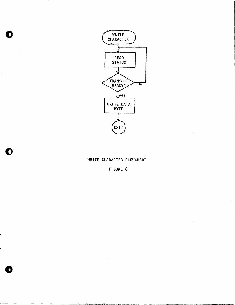
To write a character out, the flowchart in Figure 8 may be used. The first operation performed .is reading the UART status to determine if the UART transmitter is ready for a data byte. If it is, the data character is output to the data port. If the UART is not ready, the program waits until it is ready. After the character is output the subroutine exits.
To read a character in, the flowchart in Figure 9 may be used. The first operation performed is reading the UART status to determine if the UART receiver has: received a data byte. If no character has been received, the program waits until a data byte is input. When the input character has been assembled into an 8-bit wide character in the receiver, severa~ checks are made to determine if the character is valid. The parity of the character is checked against the parity bit to determine if any bits in the character were altered. An overrun error is detected if the current byte was sent while the previous byte was still in the UART. This error indicates the microprocessor system is not servicing the UART fast enough. A framing error is detected if either an incorrect number of data bits were received or if an incorrect number of stop bits were used to terminate the character. If any of these error conditions are true, an error flag in memory is set, the UART error is reset, and the subroutine exits. If the data byte is error-free, the data byte is read, the correct number of bits is masked off, and the subroutine exits.
&&£LGJWiWM&DM4NiM# ; $ 4 i A 4# UH ;4444 * .iiM&W"liMwiN&!4MWhiitf.l'iifWEiEU!9',-!H"iI,i.;;, AAIh·ij " .IH41Pf+~

WRITE BA.UD RATE
I BYTE
t
WRITE COMMAND BYTE
INITIALIZE UART FLOWCHART
FIGURE 7
1 ... -.·.·)) ',.]
o
------------------------------_._--........ _-----
o
o
o
READ STATUS
WRITE DATA BYTE
WRITE CHARACTER FLOWCHART
FIGURE 8
-=lCt L&cliND*,g"WiM&i\QU;«ALM#Ii,Ji ;; ,;; '. ;; ; '""",*,$ PH ## A4%##WPU ¢ 4 * 4. .# AM

READ STATUS
READ DATA BYTE
[ MA~K OFF DATA
~EAO CH,'RACTER FLOWCHART FIGURE 9
o

.n IAI·' i 1',1\1 ---,·A .. , 1".1
'It "l ,"'·1' '".11' 1/4.1",
~~' •• fA! ., '!'. ,·.·,rll
'~------~!I_TlE _____ .____ _ ___ .D~!~ __ . _____ ~ ..... ,.11 If II f.t' ....... '.,',
\' 00 00 "."T"~U1f. \MoT: NOP
1 ~L NOP
2 00 -.flO.?_
() 3 ~E:
"-, _?3
5 b~
'-"bAl:-.
OPA. f-.
8 FoO -7 ~E. LDA"!.
a ~A -9 1>~ OPA
A E.'-L -B 1>~ QPA
C E2. I - f.L
0 '-DA"!. ~E. ~~_~ __________ ~~!~~ ________ ~=-_~~~~'I~~L_~_h~.q~~T£~ _____________________ ~ E ~7 - P1 CCt 1)6' I>~ P3 U l)t 1)0
F ~~ OPA HOT" ust:"DJ I I I I I I I
o ' E~ -1 D~ OOA
2 E2. -3 cA {tiS
.. 5
6
7
8
9 .
A! 9
cl 01
E
F
F'~URE. \0 - \".)\'j ALl Z.E fOR ~O-$?S
0 PRO-LOG CORPORATION PROGRAM ASSEMBLY FORM
HE:rA.r::~:··~·:'L ... ~ •. : '.":""'r: TITLE DATE P ... c.~ I ~.;.; I ',5-"1 L"e~~ I ' .... 5 ~q I "'CO,F",!:R C:".·'.,'E:".75 A-:'
\\ '2..0 I Dr, Itw",T': UAR'T ,.., I \PA : ~W"'T FOil R~AT>V 1 EI.\ - !OARI ~~OL.~ 2 Eb I AN to. I- i
3 0\ I - 01 .
4 c..A I JP ~I I
5 '2.0 I - :(·..-.l~hTc=. IIAR"t 11.\ ;
5 II - • 7 7c L:llA. I M (~L) L ~S.lT(;' A~lL 8 1)3 I 9 £1. I - UA~, DATA (ii:) ~
A c..Q ~\S
B 1 c 0
F.
F
II ~o ~O l~"ft. UA~T"&) 'PA -YA1"r FI"L_..P.£AT>'1
1 E2.. - I --2 E.io AlJA7
3 0\ - 0\
.. _c..A JP 1.. 5 ~O - ~.\.!.e.J~~') 6 1\ - • -
-' 7 '7P:. LOA N\ ("'-a - 1NA.~c:.It. 8 -~.~-
I --I~" --------t
~ , EI !MLMTA (f;> t A c.,C\ t _fr'r5
0 o
C -- _-..!'- - --
E '---~. , -,
r:\~Up,S l\ - WRnc S ~ Reu T l!~ E. HD~ ~O~5
MM ., i '~i

PRO·lOG Con-PORATION PROGRAM ASSEMOl Y rORM
""A""".,."I_ 'w.'.' ~ •. ,ru,. TITLE DATE ,',A,,' 11M .,,';111 'A"', ...... ". • ... ·.'"'1111 ;:,IM,.A' "-", Al·' AI'1f
4\ 0 .. 1>1\ ~~~~ <:J-t,." .. ~tl:." ~) ,pI\., ~_"A1TJOR El(lTSt_W '~"---ATUt( J
" __ a .... _ - T
1 (~ - VA '-l:..~TI.Q)...A -AE(C,,!E. r,uea"T't.:D. -rO"et.~ At.
2 '~i -~~~- A J"IW 3 E(' . ANA1
4 O~ - 2.2. 5 C.A -!.p Z I
() IS '40 - CR"'~c:.~' 7 "
. . '
a 1ca L 'P" 1!1 c.MEe.tt.. Faa. 1>All\-r'l E'MoR
9 E" ANAl A 09 - OQ
B (.2- ! J? 70
C ('It -D lI.-. .
• I E '79 1."D1\ 'B - I F E!o ANA!.
I ~o 10 - '0 .--1 Co2 ~? ~o
2 'Ill'-- - O~eRR\)1'l uao ....
I ;J i,,, -I 4 '7 'a L'J)A
I -0 . ~c."EeK FOa. 'ffSac ...... IL E:ll«'OQ.. .--
I 5 flo A~A "I- I --j 6 'l..0 - ~
I 7 C'..2. J~ zo ! a ~'JI, I - ~~NG. f:RRoR
I 9 -..'( -: A 1l'B \~A INPUT Asc: n. ." I B E3 - ,lJART1>t>.-rA A 1 C ~fo OM1 i C S£T PAR\TY ~'T --
i~ D <ao - 90 .. -! E "17 ~"'AN (ML) "'STofli: 'H M£MOR.'f .-
,- 15 F c..q R"f5 -- _ .... "
PRO·LOG CORPORATION PROGRAM ASSEMBLY FORM o
_ ..... _ .. . '.\ .... \£~l·.4!"L • .' ... ",::'.I.or~'c TITLE DATE
-' : ,.",£ 1~;S -"I ~NSTR '.~OOIF'ER CC~ .. ~'.~= ~ 7 S ""-,,,, ;.Ae!:l
U , toO I ~D CRe~n " .. ,p~ I L WAn fD~ t:l. \'ls, \ •. H'l H 'DA.'A. I.P-J. M>=MI'':!.V
I • C.o~~OL '}, ~~('£I"r-.. Al I 1 E2. 1 - UA~T ~1"l\~\Trn 'Tn <;>"'1
1 2 ,-\7 -- \ '-):IA, A ~~~t>'i I 3 Elo IvJ 1\1 ,
4 02. - Ol. '.
i 5 CA • JP 2.1 '- I
.. -~ (cO - 1~~€Pt.'t) C."AIt~\E~ ~, . __ ~7 "
I -I 8 19 \..1>A. 1!. i'- C.~E.".K fCl~ ?A~'i,( ERRO"it
... ! 9 ElD ANAl. I A O~, - OQ
'~--r 0 C.2 JP lO -.--1 c 'IlX - W'~'TY £RRo~ _1 D ~-,c. - ~ ~.- 1 E 19 L'J)A, ~ ~~£~!S f=~ Q~€:R~UN ~!~JtOR.
~
, bF Eb A.NAo.1.
.. --1 10 \0 - \0
-1 1 ~2. JP '/...0 --1 2 ~)( - O::l~ '\lJ. oL..E&tt.QQ.
-.1 3 'A.l( ---1 4 78 \-'1>" ~ C."-E:<!.K ~~II.M\r!4 E.R!\.Q.~
----t 5 Elo ANA. :t
-----~ ~ .. 2.0
,-.~ .. ~_ 7 c.'1 JP It) -. .-.L!... ...!'-'l..- - .fAAMtH 4LEUO~_ -.-l, t "'~ . ·---L~ 'y'l\ '~A [_~~~YT~ . "---+--.!- -~ . -
~~ ··---,r-Cl.. ""~b ORAl r.J~~.t..:L-... ~-. _~O_ - jo , ... L_£ 77 SI ~~ __ (Il_L-->- ~r.ORf.._..JK-M(MO&'L -lJr ell ~'TS
----~--~~ ~ ............. . ---

o 730~ DUAL UART CARD ENVIRONMENTAL SPECIFICATIONS
RECOMMENDED OPERATING LIMITS ABSOLUTE NON-OPERATING LIMITS
PARAMETER MIN TYP MAX MIN MAX UNI.TS
Free Air Temperature 0 25 55 -40 75 °c
Humi d i ty 0 95CD 0 95CD %RH
Shock Not Specified Not Specified
Vibration .. .. EMI It " ESD .. It
CD NON-CONOENS I 'NG R~LAT I VE HUHI 0 I TY
o 7304 DUAL UART CARD ELECTRICAL SPECIFICATIONS
RECOMMENDED OPERATING LIMITS A£SOLUTE NON OPERATING LI~ITS
PARAMETER MIN TYP MAX MIN MAX UNITS
Vee 4.75 5.00 5.25 0.0 7,00 Volt
AUX +V 11.40 12.00 12.60 0.0 15.00 Vo'} t
AUX -v -12.60 -12.00 - 11 • ~O -15.0 0.0 Va 1 t
o
i;ooIQ&liJim;q=&aaIAA

RS-232C USER INTERFACE ELECTRICAL CHARACTERISTICS OVER RECOMMENDED OPERATING LIMITS .~ )
PARAMETER MIN TYP MAX UNITS
HIGH LEVEL OUTPUT VOLTAGE(j) 9.0 10.0 Vol t
LOW LEVEL OUTPUT VOLTAGE CD -10.0 -9.0 Vol t
HIGH LEVEL SHORT-CIRCUIT CURRENT +6.0 +10.0 +12.0 rnA
LOW LEVEL SHORT-CIRCUIT CURRENT -12.0 -10.0 -6.0 rnA
HIGH LEVEL INPUT THRESHOLD VOLTAGE 3.0 Vol t
LO'.>} LEVEL INPUT THRESHOLD VOLTAGE -3.0 Vol t
CD At termination resistance of 3.0K Q minimum
TTY USER INTERFACE ELECTRICAL CHARACTERISTICS OVER RECOMMENDED OPERATLNG.lIMITS
-' PARAMETER MIN TYP MAX UNITS
HIGH LEVEL OUTPUT CURRENT Ci) -0.0 mA
LCJ..I LEVEL OUTPUT CURRENT @ 25.0 mA
HIGH LEVEL INPUT CURRENT CD I .0 mA
LOW LEVEL INPUT CURRENT @ 0.00 mA
CDAt a compliance voltage of +11.40 volt minimum
@At a voltage of 0.0 volt minimum
(.)

PARAMETER MIN TYP MAX UNITS o 6. STD BUS ELECTRICAL CHARACTERISTICS OVER RECOMMENDED OPERATION LIMITS
Vee SUPPLY CURRENT 400 660 rnA
AUX +V SUPPLY CURREHT 76 120 rnA
AUX -v SUPPLY CURRENT 72 120 rnA
STD BUS INPUT LOAD See Figure 11
STD BUS OUTPUT DRIVE See Figure 11 I
6. SWITCHING CHARACTERISTICS OVER RECOMMENDED OPERATING LIMITS
PARAMETER MHj TYP MAX UNITS
RS-232C OUTPUT RATE OF CHANGE 30 V/lJsec
RS-232C BAUD RATE 9600 Baud
o CURRENT LOOP BAUD RATE 110 300 Baud
o
-= __ -=MWlh4bMi0llim:iQUiidWlW ; 4iU ; .; I fWMWWWFTMMIiFTf44Afasy;¥#T4f'l#¥ W .4 W4WF G#MF 4 A 4 P # ¢ I 4 ¢ 4

7 HICIiANICAL
Refer to Figure 13 for cpmponent pla~ement informaton. The 730~ meets all STo BUS general me~hanic~l specifications. Th~ 7304 requires one card slot in a standard STO BUS card rack.
To configure data communications Channel A for OlE or DCE modes of operation, shorting jumper block 'A' should.be moved to the 'oTE' ,or 'oCE'positions shown· in Figure 13. Physical connection to the RS-232C signals are provid~d at connrctor J3 which is a 26 pin locking male PC board header. Connection to the industry standard 25 pin '0' connector should be made with a cable link equivJlent to RC-25-M for the OTE configuration or RC-25-F for the DCE configuration. These assemblies are available from Pro-Log and are described in a scp~rJte data sheet.
~~ch0niCJl configuration of Channel B is similar to the pro~~dure for Channel A. In ad.iition, to configure Channel B for the TIV il1terface option, _ Short in<l jUr.1per block 'B' should be moved to the 'TTY' position shown in Figure 13 Physic~l connection to the current loop signals are provided at connector Jl which is also a 26 pin locking male PC board header. Connection to the Pro-Log standdrd 9 pin '0' connector should be made with a cable link equival~nt to RC- 9 -M (sec 5t!parate data sheet).
'\ i
(.)

•
•
• .. - Aiea.;as $I ¥4Q$$MA

USER'S MANUAL
----------------------_ ... ,., .. " .. ".,-
2411 Garden Road Monterey, California 93940 Telephone: (408) 372-4593
TWX: 910-360-7082
106242 B 600 9/81
o
o
o
, IIIi