PrimeCell UART (PL011) - ARM architectureinfocenter.arm.com/.../DDI0183G_uart_pl011_r1p5_trm.pdf ·...
96
Copyright © 2000, 2001, 2005, 2007 ARM Limited. All rights reserved. ARM DDI 0183G PrimeCell ® UART (PL011) Revision: r1p5 Technical Reference Manual
Transcript of PrimeCell UART (PL011) - ARM architectureinfocenter.arm.com/.../DDI0183G_uart_pl011_r1p5_trm.pdf ·...

PrimeCell® UART (PL011)Revision: r1p5
Technical Reference Manual
Copyright © 2000, 2001, 2005, 2007 ARM Limited. All rights reserved.ARM DDI 0183G
PrimeCell UART (PL011)Technical Reference Manual
Copyright © 2000, 2001, 2005, 2007 ARM Limited. All rights reserved.
Release Information
The Change history table lists the changes made to this manual.
Proprietary Notice
Words and logos marked with ® or ™ are registered trademarks or trademarks of ARM Limited in the EU and other countries, except as otherwise stated below in this proprietary notice. Other brands and names mentioned herein may be the trademarks of their respective owners.
Neither the whole nor any part of the information contained in, or the product described in, this document may be adapted or reproduced in any material form except with the prior written permission of the copyright holder.
The product described in this document is subject to continuous developments and improvements. All particulars of the product and its use contained in this document are given by ARM in good faith. However, all warranties implied or expressed, including but not limited to implied warranties of merchantability, or fitness for purpose, are excluded.
This document is intended only to assist the reader in the use of the product. ARM Limited shall not be liable for any loss or damage arising from the use of any information in this document, or any error or omission in such information, or any incorrect use of the product.
Where the term ARM is used it means “ARM or any of its subsidiaries as appropriate”.
Confidentiality Status
This document is Non-Confidential. The right to use, copy and disclose this document may be subject to license restrictions in accordance with the terms of the agreement entered into by ARM and the party that ARM delivered this document to.
Change history
Date Issue Confidentiality Change
12 July 2000 A Open Access First release.
18 August 2000 B Open Access Change to signal names in Fig 2-1, changes to bits in Figs 4-1, 4-3.
9 February 2001 C Open Access Change to Figure 2-7. Note added to para 3.3.6.
15 February 2001 D Open Access Text change to pages 2-9, and 2-12.
14 December 2001 E Open Access Text changes to pages 3-13, 3-14, and 3-17.
01 November 2005 F Non-confidential Update to add Errata 01, history of product revision, fix for defect 326409.
18 December 2007 G Non-confidential Update for r1p5. Text changes to Clock signals on page 2-10 and UARTTXINTR on page 2-23.
Buffer depth of the receive and transmit FIFOs increased.
ii Copyright © 2000, 2001, 2005, 2007 ARM Limited. All rights reserved. ARM DDI 0183G

Product Status
The information in this document is final, that is for a developed product.
Web Address
http://www.arm.com
ARM DDI 0183G Copyright © 2000, 2001, 2005, 2007 ARM Limited. All rights reserved. iii

iv Copyright © 2000, 2001, 2005, 2007 ARM Limited. All rights reserved. ARM DDI 0183G

ContentsPrimeCell UART (PL011) Technical Reference Manual
PrefaceAbout this manual ......................................................................................... xiiFeedback ..................................................................................................... xvi
Chapter 1 Introduction1.1 About the UART .......................................................................................... 1-21.2 Product revisions ........................................................................................ 1-5
Chapter 2 Functional Overview2.1 Overview ..................................................................................................... 2-22.2 Functional description ................................................................................. 2-42.3 IrDA SIR ENDEC functional description ...................................................... 2-82.4 Operation .................................................................................................. 2-102.5 UART modem operation ........................................................................... 2-162.6 UART hardware flow control ..................................................................... 2-172.7 UART DMA interface ................................................................................. 2-192.8 Interrupts ................................................................................................... 2-22
Chapter 3 Programmers Model3.1 About the programmers model .................................................................... 3-2
ARM DDI 0183G Copyright © 2000, 2001, 2005, 2007 ARM Limited. All rights reserved. v

Contents
3.2 Summary of registers ................................................................................. 3-33.3 Register descriptions .................................................................................. 3-5
Chapter 4 Programmers Model for Test4.1 Test harness overview ................................................................................ 4-24.2 Scan testing ................................................................................................ 4-34.3 Summary of test registers ........................................................................... 4-44.4 Test register descriptions ........................................................................... 4-54.5 Integration testing of block inputs ............................................................... 4-94.6 Integration testing of block outputs ........................................................... 4-114.7 Integration test summary .......................................................................... 4-14
Appendix A Signal DescriptionsA.1 AMBA APB signals ..................................................................................... A-2A.2 On-chip signals ........................................................................................... A-3A.3 Signals to pads ........................................................................................... A-5
vi Copyright © 2000, 2001, 2005, 2007 ARM Limited. All rights reserved. ARM DDI 0183G

List of TablesPrimeCell UART (PL011) Technical Reference Manual
Change history .............................................................................................................. iiTable 2-1 Receive FIFO bit functions ...................................................................................... 2-13Table 2-2 Function of the modem input/output signals in DTE and DCE modes .................... 2-16Table 2-3 Control bits to enable and disable hardware flow control ........................................ 2-17Table 2-4 DMA trigger points for the transmit and receive FIFOs ........................................... 2-21Table 3-1 UART register summary ............................................................................................ 3-3Table 3-2 UARTDR Register ..................................................................................................... 3-6Table 3-3 UARTRSR/UARTECR Register ................................................................................ 3-7Table 3-4 UARTFR Register ..................................................................................................... 3-8Table 3-5 UARTILPR Register .................................................................................................. 3-9Table 3-6 UARTIBRD Register ................................................................................................. 3-9Table 3-7 UARTFBRD Register .............................................................................................. 3-10Table 3-8 Typical baud rates and integer divisors when UARTCLK=7.3728MHz .................. 3-11Table 3-9 Integer and fractional divisors for typical baud rates when UARTCLK=4MHz ....... 3-12Table 3-10 UARTLCR_H Register ............................................................................................ 3-13Table 3-11 Parity truth table ...................................................................................................... 3-14Table 3-12 UARTCR Register ................................................................................................... 3-15Table 3-13 UARTIFLS Register ................................................................................................ 3-17Table 3-14 UARTIMSC Register ............................................................................................... 3-18Table 3-15 UARTRIS Register .................................................................................................. 3-19Table 3-16 UARTMIS Register .................................................................................................. 3-20
ARM DDI 0183G Copyright © 2000, 2001, 2005, 2007 ARM Limited. All rights reserved. vii
List of Tables
Table 3-17 UARTICR Register ................................................................................................. 3-21Table 3-18 UARTDMACR Register .......................................................................................... 3-22Table 3-19 UARTPeriphID0 Register ........................................................................................ 3-23Table 3-20 UARTPeriphID1 Register ........................................................................................ 3-24Table 3-21 UARTPeriphID2 Register ........................................................................................ 3-24Table 3-22 UARTPeriphID3 Register ........................................................................................ 3-25Table 3-23 UARTPCellID0 Register ......................................................................................... 3-26Table 3-24 UARTPCellID1 Register ......................................................................................... 3-26Table 3-25 UARTPCellID2 Register ......................................................................................... 3-26Table 3-26 UARTPCellID3 Register ......................................................................................... 3-27Table 4-1 Test registers summary ............................................................................................ 4-4Table 4-2 UARTTCR register .................................................................................................... 4-5Table 4-3 UARTITIP register .................................................................................................... 4-6Table 4-4 UARTITOP register ................................................................................................... 4-7Table 4-5 UARTTDR register .................................................................................................... 4-8Table 4-6 Integration test strategy .......................................................................................... 4-14Table A-1 APB slave interface signals ...................................................................................... A-2Table A-2 On-chip signals ......................................................................................................... A-3Table A-3 Pad signal descriptions ............................................................................................. A-5
viii Copyright © 2000, 2001, 2005, 2007 ARM Limited. All rights reserved. ARM DDI 0183G

List of FiguresPrimeCell UART (PL011) Technical Reference Manual
Key to timing diagram conventions ............................................................................ xivFigure 2-1 UART block diagram ................................................................................................. 2-4Figure 2-2 IrDA SIR ENDEC block diagram ............................................................................... 2-8Figure 2-3 Baud rate divisor ..................................................................................................... 2-11Figure 2-4 UART character frame ............................................................................................ 2-15Figure 2-5 IrDA data modulation (3/16) .................................................................................... 2-15Figure 2-6 Hardware flow control between two similar devices ................................................ 2-17Figure 2-7 DMA transfer waveforms ......................................................................................... 2-21Figure 3-1 Peripheral Identification Register bit assignments .................................................. 3-23Figure 3-2 PrimeCell Identification Register bit assignments ................................................... 3-25Figure 4-1 Input integration test harness .................................................................................... 4-9Figure 4-2 Output integration test harness, intra-chip outputs ................................................. 4-12Figure 4-3 Output integration test harness, primary outputs .................................................... 4-13
ARM DDI 0183G Copyright © 2000, 2001, 2005, 2007 ARM Limited. All rights reserved. ix

List of Figures
x Copyright © 2000, 2001, 2005, 2007 ARM Limited. All rights reserved. ARM DDI 0183G

Preface
This preface introduces the PrimeCell UART (PL011) Technical Reference Manual. It contains the following sections:
• About this manual on page xii
• Additional reading on page xv
• Feedback on page xvi.
ARM DDI 0183G Copyright © 2000, 2001, 2005, 2007 ARM Limited. All rights reserved. xi

Preface
About this manual
This is the Technical Reference Manual (TRM) for the PrimeCell UART (PL011).
Product revision status
The rnpn identifier indicates the revision status of the product described in this manual, where:
rn Identifies the major revision of the product.
pn Identifies the minor revision or modification status of the product.
Intended audience
This manual has been written for hardware and software engineers implementing System-on-Chip designs. It provides information to enable designers to integrate the peripheral into a target system as quickly as possible.
Using this manual
This manual is organized into the following chapters:
Chapter 1 Introduction
Read this chapter for an introduction to the UART.
Chapter 2 Functional Overview
Read this chapter for a description of the major functional blocks of the UART.
Chapter 3 Programmers Model
Read this chapter for a description of the UART memory map and registers.
Chapter 4 Programmers Model for Test
Read this chapter for a description of the logic in the UART for integration testing.
Appendix A Signal Descriptions
Read this appendix for a description of the UART input and output signals.
xii Copyright © 2000, 2001, 2005, 2007 ARM Limited. All rights reserved. ARM DDI 0183G

Preface
Conventions
Conventions that this manual can use are described in:
• Typographical
• Timing diagrams
• Signals on page xiv
• Numbering on page xiv.
Typographical
The typographical conventions are:
italic Highlights important notes, introduces special terminology, denotes internal cross-references, and citations.
bold Highlights interface elements, such as menu names. Denotes signal names. Also used for terms in descriptive lists, where appropriate.
monospace Denotes text that you can enter at the keyboard, such as commands, file and program names, and source code.
monospace Denotes a permitted abbreviation for a command or option. You can enter the underlined text instead of the full command or option name.
monospace italic Denotes arguments to monospace text where the argument is to be replaced by a specific value.
monospace bold Denotes language keywords when used outside example code.
< and > Enclose replaceable terms for assembler syntax where they appear in code or code fragments. For example:
MRC p15, 0 <Rd>, <CRn>, <CRm>, <Opcode_2>
Timing diagrams
The figure named Key to timing diagram conventions on page xiv explains the components used in timing diagrams. Variations, when they occur, have clear labels. You must not assume any timing information that is not explicit in the diagrams.
Shaded bus and signal areas are undefined, so the bus or signal can assume any value within the shaded area at that time. The actual level is unimportant and does not affect normal operation.
ARM DDI 0183G Copyright © 2000, 2001, 2005, 2007 ARM Limited. All rights reserved. xiii

Preface
Key to timing diagram conventions
Signals
The signal conventions are:
Signal level The level of an asserted signal depends on whether the signal is active-HIGH or active-LOW. Asserted means:
• HIGH for active-HIGH signals
• LOW for active-LOW signals.
Lower-case n At the start or end of a signal name denotes an active-LOW signal.
Prefix H Denotes Advanced High-performance Bus (AHB) signals.
Prefix P Denotes Advanced Peripheral Bus (APB) signals.
Numbering
The numbering convention is:
<size in bits>'<base><number>
This is a Verilog® method of abbreviating constant numbers. For example:
• 'h7B4 is an unsized hexadecimal value.
• 'o7654 is an unsized octal value.
• 8'd9 is an eight-bit wide decimal value of 9.
• 8'h3F is an eight-bit wide hexadecimal value of 0x3F. This is equivalent to b00111111.
• 8'b1111 is an eight-bit wide binary value of b00001111.
xiv Copyright © 2000, 2001, 2005, 2007 ARM Limited. All rights reserved. ARM DDI 0183G

Preface
Additional reading
This section lists publications by ARM and by third parties. You can access ARM documentation at:
http://infocenter.arm.com/help/index.jsp
ARM publications
This manual contains information that is specific to the UART. See the following documents for other relevant information:
• AMBA® Specification (Rev 2.0) (ARM IHI 0011)
• ARM PrimeCell UART (PL011) Design Manual (PL011 DDES 0000)
• ARM PrimeCell UART (PL011) Integration Manual (PL011 INTM 0000).
Other publications
This section lists relevant documents published by third parties.
• Infrared Data Association®, IrDA® Physical Layer Specification v1.1, obtainable at http://www.irda.org
• Agilent Technologies, Agilent IrDA Data Link Design Guide (5988-9321E. March 2003), obtainable at http://www.agilent.com.
ARM DDI 0183G Copyright © 2000, 2001, 2005, 2007 ARM Limited. All rights reserved. xv

Preface
Feedback
ARM welcomes feedback on the PrimeCell UART (PL011) and its documentation.
Feedback on this product
If you have any comments or suggestions about this product, contact your supplier and give:
• the product name
• a concise explanation.
Feedback on this manual
If you have any comments on this manual, send an email to [email protected]. Give:
• the title
• the number
• the relevant page number(s) to which your comments apply
• a concise explanation of your comments.
ARM also welcomes general suggestions for additions and improvements.
xvi Copyright © 2000, 2001, 2005, 2007 ARM Limited. All rights reserved. ARM DDI 0183G

Chapter 1 Introduction
This chapter introduces the UART (PL011). It contains the following sections:
• About the UART on page 1-2.
• Product revisions on page 1-5.
ARM DDI 0183G Copyright © 2000, 2001, 2005, 2007 ARM Limited. All rights reserved. 1-1
Introduction
1.1 About the UART
The UART is an Advanced Microcontroller Bus Architecture (AMBA) compliant System-on-Chip (SoC) peripheral that is developed, tested, and licensed by ARM.
The UART is an AMBA slave module that connects to the Advanced Peripheral Bus (APB). The UART includes an Infrared Data Association (IrDA) Serial InfraRed (SIR) protocol ENcoder/DECoder (ENDEC).
The features of the UART are described in the following sections:
• Features
• Programmable parameters on page 1-3
• Variations from the 16C650 UART on page 1-4.
Note Because of changes in the programmers model, the UART (PL011) is not backwards compatible with the previous PrimeCell UART (PL010).
1.1.1 Features
The UART provides:
• Compliance to the AMBA Specification (Rev 2.0) onwards for easy integration into SoC implementation.
• Programmable use of UART or IrDA SIR input/output.
• Separate 32×8 transmit and 32×12 receive First-In, First-Out (FIFO) memory buffers to reduce CPU interrupts.
• Programmable FIFO disabling for 1-byte depth.
• Programmable baud rate generator. This enables division of the reference clock by (1×16) to (65535×16) and generates an internal ×16 clock. The divisor can be a fractional number enabling you to use any clock with a frequency >3.6864MHz as the reference clock.
• Standard asynchronous communication bits (start, stop and parity). These are added prior to transmission and removed on reception.
• Independent masking of transmit FIFO, receive FIFO, receive timeout, modem status, and error condition interrupts.
• Support for Direct Memory Access (DMA).
• False start bit detection.
1-2 Copyright © 2000, 2001, 2005, 2007 ARM Limited. All rights reserved. ARM DDI 0183G

Introduction
• Line break generation and detection.
• Support of the modem control functions CTS, DCD, DSR, RTS, DTR, and RI.
• Programmable hardware flow control.
• Fully-programmable serial interface characteristics:
— data can be 5, 6, 7, or 8 bits
— even, odd, stick, or no-parity bit generation and detection
— 1 or 2 stop bit generation
— baud rate generation, dc up to UARTCLK/16
• IrDA SIR ENDEC block providing:
— programmable use of IrDA SIR or UART input/output
— support of IrDA SIR ENDEC functions for data rates up to 115200 bps half-duplex
— support of normal 3/16 and low-power (1.41-2.23µs) bit durations
— programmable division of the UARTCLK reference clock to generate the appropriate bit duration for low-power IrDA mode.
• Identification registers that uniquely identify the UART. These can be used by an operating system to automatically configure itself.
1.1.2 Programmable parameters
The following key parameters are programmable:
• communication baud rate, integer, and fractional parts
• number of data bits
• number of stop bits
• parity mode
• FIFO enable (32 deep) or disable (1 deep)
• FIFO trigger levels selectable between 1/8, 1/4, 1/2, 3/4, and 7/8• internal nominal 1.8432MHz clock frequency (1.42-2.12MHz) to generate
low-power IrDA mode shorter bit duration
• hardware flow control.
Additional test registers and modes are implemented for integration testing.
ARM DDI 0183G Copyright © 2000, 2001, 2005, 2007 ARM Limited. All rights reserved. 1-3

Introduction
1.1.3 Variations from the 16C650 UART
The UART varies from the industry-standard 16C650 UART device as follows:
• receive FIFO trigger levels are 1/8, 1/4, 1/2, 3/4, and 7/8
• transmit FIFO trigger levels are 1/8, 1/4, 1/2, 3/4, and 7/8• the internal register map address space, and the bit function of each register differ
• the deltas of the modem status signals are not available.
The following 16C650 UART features are not supported:
• 1.5 stop bits (1 or 2 stop bits only are supported)
• independent receive clock.
1-4 Copyright © 2000, 2001, 2005, 2007 ARM Limited. All rights reserved. ARM DDI 0183G

Introduction
1.2 Product revisions
This section describes the differences in functionality between product revisions of the UART:
r1p0-r1p1 Contains the following differences in functionality:
• The Revision field in the UARTPeriphID2 Register on page 3-24 bits [7:4] now reads back as 0x1.
r1p1-r1p3 Contains the following differences in functionality:
• The Revision field in the UARTPeriphID2 Register on page 3-24 bits [7:4] now reads back as 0x2.
r1p3-r1p4 Contains the following differences in functionality:
• The Revision field in the UARTPeriphID2 Register on page 3-24 bits [7:4] now reads back as 0x2.
r1p4-r1p5 Contains the following differences in functionality:
• The receive and transmit FIFOs are increased to a depth of 32.
• The Revision field in the UARTPeriphID2 Register on page 3-24 bits [7:4] now reads back as 0x3.
Note See the engineering errata that accompanies the product deliverables, for information about any functional differences that a later revision provides.
ARM DDI 0183G Copyright © 2000, 2001, 2005, 2007 ARM Limited. All rights reserved. 1-5

Introduction
1-6 Copyright © 2000, 2001, 2005, 2007 ARM Limited. All rights reserved. ARM DDI 0183G

Chapter 2 Functional Overview
This chapter describes the major functional blocks of the UART. It contains the following sections:
• Overview on page 2-2
• Functional description on page 2-4
• IrDA SIR ENDEC functional description on page 2-8
• Operation on page 2-10
• UART modem operation on page 2-16
• UART hardware flow control on page 2-17
• UART DMA interface on page 2-19
• Interrupts on page 2-22.
ARM DDI 0183G Copyright © 2000, 2001, 2005, 2007 ARM Limited. All rights reserved. 2-1
Functional Overview
2.1 Overview
The UART performs:
• serial-to-parallel conversion on data received from a peripheral device
• parallel-to-serial conversion on data transmitted to the peripheral device.
The CPU reads and writes data and control/status information through the AMBA APB interface. The transmit and receive paths are buffered with internal FIFO memories enabling up to 32-bytes to be stored independently in both transmit and receive modes.
The UART:
• includes a programmable baud rate generator that generates a common transmit and receive internal clock from the UART internal reference clock input, UARTCLK
• offers similar functionality to the industry-standard 16C650 UART device
• supports the following maximum baud rates:
— 921600 bps, in UART mode
— 460800 bps, in IrDA mode
— 115200 bps, in low-power IrDA mode.
The UART operation and baud rate values are controlled by the Line Control Register, UARTLCR_H on page 3-12 and the baud rate divisor registers (Integer Baud Rate Register, UARTIBRD on page 3-9 and Fractional Baud Rate Register, UARTFBRD on page 3-10).
The UART can generate:
• individually-maskable interrupts from the receive (including timeout), transmit, modem status and error conditions
• a single combined interrupt so that the output is asserted if any of the individual interrupts are asserted, and unmasked
• DMA request signals for interfacing with a Direct Memory Access (DMA) controller.
If a framing, parity, or break error occurs during reception, the appropriate error bit is set, and is stored in the FIFO. If an overrun condition occurs, the overrun register bit is set immediately and FIFO data is prevented from being overwritten.
You can program the FIFOs to be 1-byte deep providing a conventional double-buffered UART interface.
2-2 Copyright © 2000, 2001, 2005, 2007 ARM Limited. All rights reserved. ARM DDI 0183G

Functional Overview
The modem status input signals Clear To Send (CTS), Data Carrier Detect (DCD), Data Set Ready (DSR), and Ring Indicator (RI) are supported. The output modem control lines, Request To Send (RTS), and Data Terminal Ready (DTR) are also supported.
There is a programmable hardware flow control feature that uses the nUARTCTS input and the nUARTRTS output to automatically control the serial data flow.
2.1.1 IrDA SIR block
The IrDA Serial InfraRed (SIR) block contains an IrDA SIR protocol ENDEC. The SIR protocol ENDEC can be enabled for serial communication through signals nSIROUT and SIRIN to an infrared transducer instead of using the UART signals UARTTXD and UARTRXD.
If the SIR protocol ENDEC is enabled, the UARTTXD line is held in the passive state (HIGH) and transitions of the modem status, or the UARTRXD line have no effect. The SIR protocol ENDEC can receive and transmit, but it is half-duplex only, so it cannot receive while transmitting, or transmit while receiving.
The IrDA SIR physical layer specifies a minimum 10ms delay between transmission and reception.
ARM DDI 0183G Copyright © 2000, 2001, 2005, 2007 ARM Limited. All rights reserved. 2-3

Functional Overview
2.2 Functional description
Figure 2-1 shows a block diagram of the UART.
Figure 2-1 UART block diagram
2-4 Copyright © 2000, 2001, 2005, 2007 ARM Limited. All rights reserved. ARM DDI 0183G

Functional Overview
Note Test logic is not shown for clarity.
The functions of the UART are described in the following sections:
• AMBA APB interface
• Register block
• Baud rate generator
• Transmit FIFO
• Receive FIFO on page 2-6
• Transmit logic on page 2-6
• Receive logic on page 2-6
• Interrupt generation logic on page 2-6
• DMA interface on page 2-6
• Synchronizing registers and logic on page 2-7
• Test registers and logic on page 2-7.
2.2.1 AMBA APB interface
The AMBA APB interface generates read and write decodes for accesses to status/control registers, and the transmit and receive FIFOs.
2.2.2 Register block
The register block stores data written, or to be read across the AMBA APB interface.
2.2.3 Baud rate generator
The baud rate generator contains free-running counters that generate the internal ×16 clocks, Baud16 and IrLPBaud16 signals. Baud16 provides timing information for UART transmit and receive control. Baud16 is a stream of pulses with a width of one UARTCLK clock period and a frequency of 16 times the baud rate. IrLPBaud16 provides timing information to generate the pulse width of the IrDA encoded transmit bit stream when in low-power IrDA mode.
2.2.4 Transmit FIFO
The transmit FIFO is an 8-bit wide, 32 location deep, FIFO memory buffer. CPU data written across the APB interface is stored in the FIFO until read out by the transmit logic. You can disable the transmit FIFO to act like a one-byte holding register.
ARM DDI 0183G Copyright © 2000, 2001, 2005, 2007 ARM Limited. All rights reserved. 2-5

Functional Overview
2.2.5 Receive FIFO
The receive FIFO is a 12-bit wide, 32 location deep, FIFO memory buffer. Received data and corresponding error bits, are stored in the receive FIFO by the receive logic until read out by the CPU across the APB interface. The receive FIFO can be disabled to act like a one-byte holding register.
2.2.6 Transmit logic
The transmit logic performs parallel-to-serial conversion on the data read from the transmit FIFO. Control logic outputs the serial bit stream beginning with a start bit, data bits with the Least Significant Bit (LSB) first, followed by the parity bit, and then the stop bits according to the programmed configuration in control registers.
2.2.7 Receive logic
The receive logic performs serial-to-parallel conversion on the received bit stream after a valid start pulse has been detected. Overrun, parity, frame error checking, and line break detection are also performed, and their status accompanies the data that is written to the receive FIFO.
2.2.8 Interrupt generation logic
Individual maskable active HIGH interrupts are generated by the UART. A combined interrupt output is also generated as an OR function of the individual interrupt requests.
You can use the single combined interrupt with a system interrupt controller that provides another level of masking on a per-peripheral basis. This enables you to use modular device drivers that always know where to find the interrupt source control register bits.
You can also use the individual interrupt requests with a system interrupt controller that provides masking for the outputs of each peripheral. In this way, a global interrupt service routine can read the entire set of sources from one wide register in the system interrupt controller. This is attractive where the time to read from the peripheral registers is significant compared to the CPU clock speed in a real-time system.
See Interrupts on page 2-22 for more information.
2.2.9 DMA interface
The UART provides an interface to connect to the DMA controller as UART DMA interface on page 2-19 describes.
2-6 Copyright © 2000, 2001, 2005, 2007 ARM Limited. All rights reserved. ARM DDI 0183G

Functional Overview
2.2.10 Synchronizing registers and logic
The UART supports both asynchronous and synchronous operation of the clocks, PCLK and UARTCLK. Synchronization registers and handshaking logic have been implemented, and are active at all times. This has a minimal impact on performance or area. Synchronization of control signals is performed on both directions of data flow, that is from the PCLK to the UARTCLK domain, and from the UARTCLK to the PCLK domain.
2.2.11 Test registers and logic
There are registers and logic for functional block verification, and integration testing using TicTalk or code based vectors.
Test registers must not be read or written to during normal use.
The integration testing verifies that the UART has been wired into a system correctly. It enables each input and output to be both written to and read.
ARM DDI 0183G Copyright © 2000, 2001, 2005, 2007 ARM Limited. All rights reserved. 2-7

Functional Overview
2.3 IrDA SIR ENDEC functional description
The IrDA SIR ENDEC comprises:
• IrDA SIR transmit encoder
• IrDA SIR receive decoder on page 2-9.
Figure 2-2 shows a block diagram of the IrDA SIR ENDEC.
Figure 2-2 IrDA SIR ENDEC block diagram
2.3.1 IrDA SIR transmit encoder
The SIR transmit encoder modulates the Non Return-to-Zero (NRZ) transmit bit stream output from the UART. The IrDA SIR physical layer specifies use of a Return To Zero, Inverted (RZI) modulation scheme that represents logic 0 as an infrared light pulse. The modulated output pulse stream is transmitted to an external output driver and infrared Light Emitting Diode (LED).
In IrDA mode the transmitted pulse width is specified as three times the period of the internal ×16 clock (Baud16), that is, 3/16 of a bit period.
In low-power IrDA mode the transmit pulse width is specified as 3/16 of a 115200 bps bit period. This is implemented as three times the period of a nominal 1.8432MHz clock (IrLPBaud16) derived from dividing down of UARTCLK clock. The frequency of IrLPBaud16 is set up by writing the appropriate divisor value to the IrDA Low-Power Counter Register, UARTILPR on page 3-9.
2-8 Copyright © 2000, 2001, 2005, 2007 ARM Limited. All rights reserved. ARM DDI 0183G

Functional Overview
The active low encoder output is normally LOW for the marking state (no light pulse). The encoder outputs a high pulse to generate an infrared light pulse representing a logic 0 or spacing state.
In normal and low-power IrDA modes, when the fractional baud rate divider is used, the transmitted SIR pulse stream includes an increased amount of jitter. This jitter is because the Baud16 pulses cannot be generated at regular intervals when fractional division is used. That is, the Baud16 cycles have a different number of UARTCLK cycles. It can be shown that the worst case jitter in the SIR pulse stream can be up to three UARTCLK cycles. This is within the limits of the SIR IrDA Specification where the maximum amount of jitter permitted is 13%, provided the UARTCLK is > 3.6864MHz and the maximum baud rate used for IrDA mode is ≤ 115200 bps. With these conditions, the jitter is less than 9%.
2.3.2 IrDA SIR receive decoder
The SIR receive decoder demodulates the return-to-zero bit stream from the infrared detector and outputs the received NRZ serial bit stream to the UART received data input. The decoder input is normally HIGH (marking state) in the idle state. The transmit encoder output has the opposite polarity to the decoder input.
A start bit is detected when the decoder input is LOW.
Note To prevent the UART from responding to glitches on the received data input then it ignores SIRIN pulses that are less than:
• 3/16 of Baud16, in IrDA mode
• 3/16 of IrLPBaud16, in low-power IrDA mode.
ARM DDI 0183G Copyright © 2000, 2001, 2005, 2007 ARM Limited. All rights reserved. 2-9

Functional Overview
2.4 Operation
The operation of the UART is described in the following sections:
• Interface reset
• Clock signals
• UART operation on page 2-11
• IrDA SIR operation on page 2-14
• UART character frame on page 2-15
• IrDA data modulation on page 2-15.
2.4.1 Interface reset
The UART and IrDA SIR ENDEC are reset by the global reset signal PRESETn and a block-specific reset signal nUARTRST. An external reset controller must use PRESETn to assert nUARTRST asynchronously and negate it synchronously to UARTCLK. PRESETn must be asserted LOW for a period long enough to reset the slowest block in the on-chip system, and then be taken HIGH again. The UART requires PRESETn to be asserted LOW for at least one period of PCLK.
The values of the registers after reset are described in Chapter 3 Programmers Model.
2.4.2 Clock signals
The frequency selected for UARTCLK must accommodate the required range of baud rates:
• FUARTCLK (min) ≥ 16 × baud_rate(max)
• FUARTCLK(max) ≤ 16 × 65535 × baud_rate(min)
For example, for a range of baud rates from 110 baud to 460800 baud the UARTCLK frequency must be between 7.3728MHz to 115.34MHz.
The frequency of UARTCLK must also be within the required error limits for all baud rates to be used.
There is also a constraint on the ratio of clock frequencies for PCLK to UARTCLK. The frequency of UARTCLK must be no more than 5/3 times faster than the frequency of PCLK:
• FUARTCLK ≤ 5/3 × FPCLK
For example, in UART mode, to generate 921600 baud when UARTCLK is 14.7456MHz then PCLK must be greater than or equal to 8.85276MHz. This ensures that the UART has sufficient time to write the received data to the receive FIFO.
2-10 Copyright © 2000, 2001, 2005, 2007 ARM Limited. All rights reserved. ARM DDI 0183G
Functional Overview
2.4.3 UART operation
Control data is written to the UART Line Control Register, UARTLCR. This register is 30-bits wide internally, but is externally accessed through the APB interface by writes to the following registers:
UARTLCR_H Defines the:
• transmission parameters
• word length
• buffer mode
• number of transmitted stop bits
• parity mode
• break generation.
UARTIBRD Defines the integer baud rate divider
UARTFBRD Defines the fractional baud rate divider
Fractional baud rate divider
The baud rate divisor is a 22-bit number consisting of a 16-bit integer and a 6-bit fractional part. This is used by the baud rate generator to determine the bit period. The fractional baud rate divider enables the use of any clock with a frequency >3.6864MHz to act as UARTCLK, while it is still possible to generate all the standard baud rates.
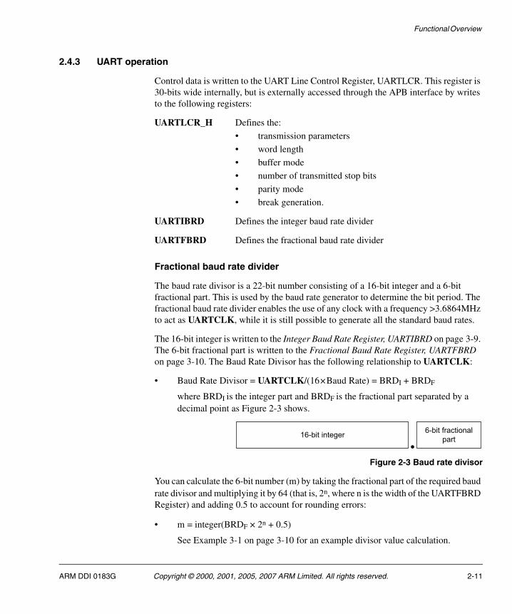
The 16-bit integer is written to the Integer Baud Rate Register, UARTIBRD on page 3-9. The 6-bit fractional part is written to the Fractional Baud Rate Register, UARTFBRD on page 3-10. The Baud Rate Divisor has the following relationship to UARTCLK:
• Baud Rate Divisor = UARTCLK/(16×Baud Rate) = BRDI + BRDF
where BRDI is the integer part and BRDF is the fractional part separated by a decimal point as Figure 2-3 shows.
Figure 2-3 Baud rate divisor
You can calculate the 6-bit number (m) by taking the fractional part of the required baud rate divisor and multiplying it by 64 (that is, 2n, where n is the width of the UARTFBRD Register) and adding 0.5 to account for rounding errors:
• m = integer(BRDF × 2n + 0.5)
See Example 3-1 on page 3-10 for an example divisor value calculation.
ARM DDI 0183G Copyright © 2000, 2001, 2005, 2007 ARM Limited. All rights reserved. 2-11

Functional Overview
An internal clock enable signal, Baud16, is generated, and is a stream of one UARTCLK wide pulses with an average frequency of 16 times the required baud rate. This signal is then divided by 16 to give the transmit clock. A low number in the baud rate divisor gives a short bit period, and a high number in the baud rate divisor gives a long bit period.
Data transmission or reception
Data received or transmitted is stored in two 32-byte FIFOs, though the receive FIFO has an extra four bits per character for status information.
For transmission, data is written into the transmit FIFO. If the UART is enabled, it causes a data frame to start transmitting with the parameters indicated in the Line Control Register, UARTLCR_H on page 3-12. Data continues to be transmitted until there is no data left in the transmit FIFO. The BUSY signal goes HIGH as soon as data is written to the transmit FIFO (that is, the FIFO is non-empty) and remains asserted HIGH while data is being transmitted. BUSY is negated only when the transmit FIFO is empty, and the last character has been transmitted from the shift register, including the stop bits. BUSY can be asserted HIGH even though the UART might no longer be enabled.
For each sample of data, three readings are taken and the majority value is kept. In the following paragraphs the middle sampling point is defined, and one sample is taken either side of it.
When the receiver is idle (UARTRXD continuously 1, in the marking state) and a LOW is detected on the data input (a start bit has been received), the receive counter, with the clock enabled by Baud16, begins running and data is sampled on the eighth cycle of that counter in UART mode, or the fourth cycle of the counter in SIR mode to allow for the shorter logic 0 pulses (half way through a bit period).
The start bit is valid if UARTRXD is still LOW on the eighth cycle of Baud16, otherwise a false start bit is detected and it is ignored.
If the start bit was valid, successive data bits are sampled on every 16th cycle of Baud16 (that is, one bit period later) according to the programmed length of the data characters. The parity bit is then checked if parity mode was enabled.
Lastly, a valid stop bit is confirmed if UARTRXD is HIGH, otherwise a framing error has occurred. When a full word is received, the data is stored in the receive FIFO, with any error bits associated with that word (see Table 2-1 on page 2-13).
2-12 Copyright © 2000, 2001, 2005, 2007 ARM Limited. All rights reserved. ARM DDI 0183G

Functional Overview
Error bits
Three error bits are stored in bits [10:8] of the receive FIFO, and are associated with a particular character. There is an additional error that indicates an overrun error and this is stored in bit 11 of the receive FIFO.
Overrun bit
The overrun bit is not associated with the character in the receive FIFO. The overrun error is set when the FIFO is full, and the next character is completely received in the shift register. The data in the shift register is overwritten, but it is not written into the FIFO. When an empty location is available in the receive FIFO, and another character is received, the state of the overrun bit is copied into the receive FIFO along with the received character. The overrun state is then cleared. Table 2-1 lists the bit functions of the receive FIFO.
Disabling the FIFOs
Additionally, you can disable the FIFOs. In this case, the transmit and receive sides of the UART have 1-byte holding registers (the bottom entry of the FIFOs). The overrun bit is set when a word has been received, and the previous one was not yet read. In this implementation, the FIFOs are not physically disabled, but the flags are manipulated to give the illusion of a 1-byte register. When the FIFOs are disabled, a write to the data register bypasses the holding register unless the transmit shift register is already in use.
System and diagnostic loopback testing
You can perform loopback testing for UART data by setting the Loop Back Enable (LBE) bit to 1 in the Control Register, UARTCR on page 3-15.
Data transmitted on UARTTXD is received on the UARTRXD input.
Table 2-1 Receive FIFO bit functions
FIFO bit Function
11 Overrun indicator
10 Break error
9 Parity error
8 Framing error
7:0 Received data
ARM DDI 0183G Copyright © 2000, 2001, 2005, 2007 ARM Limited. All rights reserved. 2-13

Functional Overview
2.4.4 IrDA SIR operation
The IrDA SIR ENDEC provides functionality that converts between an asynchronous UART data stream, and half-duplex serial SIR interface. No analog processing is performed on-chip. The role of the SIR ENDEC is to provide a digital encoded output, and decoded input to the UART. There are two modes of operation:
• In IrDA mode, a zero logic level is transmitted as high pulse of 3/16th duration of the selected baud rate bit period on the nSIROUT signal, while logic one levels are transmitted as a static LOW signal. These levels control the driver of an infrared transmitter, sending a pulse of light for each zero. On the reception side, the incoming light pulses energize the photo transistor base of the receiver, pulling its output LOW. This drives the SIRIN signal LOW.
• In low-power IrDA mode, the width of the transmitted infrared pulse is set to three times the period of the internally generated IrLPBaud16 signal (1.63µs, assuming a nominal 1.8432MHz frequency) by setting the SIRLP bit in the Control Register, UARTCR on page 3-15.
In normal and low-power IrDA modes:
• during transmission, the UART data bit is used as the base for encoding
• during reception, the decoded bits are transferred to the UART receive logic.
The IrDA SIR physical layer specifies a half-duplex communication link, with a minimum 10ms delay between transmission and reception. This delay must be generated by software because it is not supported by the UART. The delay is required because the Infrared receiver electronics might become biased, or even saturated from the optical power coupled from the adjacent transmitter LED. This delay is known as latency, or receiver setup time.
The IrLPBaud16 signal is generated by dividing down the UARTCLK signal according to the low-power divisor value written to the IrDA Low-Power Counter Register, UARTILPR on page 3-9.
The low-power divisor value is calculated as:
• Low-power divisor = (FUARTCLK / FIrLPBaud16)
where FIrLPBaud16 is nominally 1.8432MHz.
The divisor must be chosen so that 1.42MHz < FIrLPBaud16 < 2.12MHz.
System and diagnostic loopback testing
It is possible to perform loopback testing for SIR data by:
• setting the LBE bit to 1 in the Control Register, UARTCR on page 3-15.
2-14 Copyright © 2000, 2001, 2005, 2007 ARM Limited. All rights reserved. ARM DDI 0183G

Functional Overview
• setting the SIRTEST bit to 1 in the Test Control Register, UARTTCR on page 4-5.
Data transmitted on nSIROUT is received on the SIRIN input.
Note This is the only occasion that a test register is accessed during normal operation.
2.4.5 UART character frame
Figure 2-4 shows the UART character frame.
Figure 2-4 UART character frame
2.4.6 IrDA data modulation
Figure 2-5 shows the effect of IrDA 3/16 data modulation.
Figure 2-5 IrDA data modulation (3/16)
ARM DDI 0183G Copyright © 2000, 2001, 2005, 2007 ARM Limited. All rights reserved. 2-15

Functional Overview
2.5 UART modem operation
You can use the UART to support both the Data Terminal Equipment (DTE) and Data Communication Equipment (DCE) modes of operation. Figure 2-1 on page 2-4 shows the modem signals in the DTE mode. For DCE mode, Table 2-2 lists the function of the signals.
Table 2-2 Function of the modem input/output signals in DTE and DCE modes
SignalFunction
DTE DCE
nUARTCTS Clear to send Request to send
nUARTDSR Data set ready Data terminal ready
nUARTDCD Data carrier detect -
nUARTRI Ring indicator -
nUARTRTS Request to send Clear to send
nUARTDTR Data terminal ready Data set ready
nUARTOUT1 - Data carrier detect
nUARTOUT2 - Ring indicator
2-16 Copyright © 2000, 2001, 2005, 2007 ARM Limited. All rights reserved. ARM DDI 0183G

Functional Overview
2.6 UART hardware flow control
The hardware flow control feature is fully selectable, and enables you to control the serial data flow by using the nUARTRTS output and nUARTCTS input signals. Figure 2-6 shows how two devices can communicate with each other using hardware flow control.
Figure 2-6 Hardware flow control between two similar devices
When the RTS flow control is enabled, nUARTRTS is asserted until the receive FIFO is filled up to the programmed watermark level. When the CTS flow control is enabled, the transmitter can only transmit data when nUARTCTS is asserted.
The hardware flow control is selectable using the RTSEn and CTSEn bits in the Control Register, UARTCR on page 3-15. Table 2-3 lists how you must set the bits to enable RTS and CTS flow control both simultaneously, and independently.
Note When RTS flow control is enabled, the software cannot use the RTSEn bit in the Control Register, UARTCR on page 3-15 to control the status of nUARTRTS.
Table 2-3 Control bits to enable and disable hardware flow control
UARTCR Register bits
CTSEn RTSEn Description
1 1 Both RTS and CTS flow control enabled
1 0 Only CTS flow control enabled
0 1 Only RTS flow control enabled
0 0 Both RTS and CTS flow control disabled
ARM DDI 0183G Copyright © 2000, 2001, 2005, 2007 ARM Limited. All rights reserved. 2-17

Functional Overview
2.6.1 RTS flow control
The RTS flow control logic is linked to the programmable receive FIFO watermark levels. When RTS flow control is enabled, the nUARTRTS is asserted until the receive FIFO is filled up to the watermark level. When the receive FIFO watermark level is reached, the nUARTRTS signal is deasserted, indicating that there is no more room to receive any more data. The transmission of data is expected to cease after the current character has been transmitted.
The nUARTRTS signal is reasserted when data has been read out of the receive FIFO so that it is filled to less than the watermark level. If RTS flow control is disabled and the UART is still enabled, then data is received until the receive FIFO is full, or no more data is transmitted to it.
2.6.2 CTS flow control
If CTS flow control is enabled, then the transmitter checks the nUARTCTS signal before transmitting the next byte. If the nUARTCTS signal is asserted, it transmits the byte otherwise transmission does not occur.
The data continues to be transmitted while nUARTCTS is asserted, and the transmit FIFO is not empty. If the transmit FIFO is empty and the nUARTCTS signal is asserted no data is transmitted.
If the nUARTCTS signal is deasserted and CTS flow control is enabled, then the current character transmission is completed before stopping. If CTS flow control is disabled and the UART is enabled, then the data continues to be transmitted until the transmit FIFO is empty.
2-18 Copyright © 2000, 2001, 2005, 2007 ARM Limited. All rights reserved. ARM DDI 0183G
Functional Overview
2.7 UART DMA interface
The UART provides an interface to connect to a DMA controller. The DMA operation of the UART is controlled using the DMA Control Register, UARTDMACR on page 3-22. The DMA interface includes the following signals:
For receive:
UARTRXDMASREQ
Single character DMA transfer request, asserted by the UART. For receive, one character consists of up to 12 bits. This signal is asserted when the receive FIFO contains at least one character.
UARTRXDMABREQ
Burst DMA transfer request, asserted by the UART. This signal is asserted when the receive FIFO contains more characters than the programmed watermark level. You can program the watermark level for each FIFO using the Interrupt FIFO Level Select Register, UARTIFLS on page 3-17.
UARTRXDMACLR
DMA request clear, asserted by a DMA controller to clear the receive request signals. If DMA burst transfer is requested, the clear signal is asserted during the transfer of the last data in the burst.
For transmit:
UARTTXDMASREQ
Single character DMA transfer request, asserted by the UART. For transmit one character consists of up to eight bits. This signal is asserted when there is at least one empty location in the transmit FIFO.
UARTTXDMABREQ
Burst DMA transfer request, asserted by the UART. This signal is asserted when the transmit FIFO contains less characters than the watermark level. You can program the watermark level for each FIFO using the Interrupt FIFO Level Select Register, UARTIFLS on page 3-17.
UARTTXDMACLR
DMA request clear, asserted by a DMA controller to clear the transmit request signals. If DMA burst transfer is requested, the clear signal is asserted during the transfer of the last data in the burst.
ARM DDI 0183G Copyright © 2000, 2001, 2005, 2007 ARM Limited. All rights reserved. 2-19

Functional Overview
The burst transfer and single transfer request signals are not mutually exclusive, they can both be asserted at the same time. For example, when there is more data than the watermark level in the receive FIFO, the burst transfer request and the single transfer request are asserted. When the amount of data left in the receive FIFO is less than the watermark level, the single request only is asserted. This is useful for situations where the number of characters left to be received in the stream is less than a burst.
For example, if 19 characters have to be received and the watermark level is programmed to be four. The DMA controller then transfers four bursts of four characters and three single transfers to complete the stream.
Note For the remaining three characters the UART cannot assert the burst request.
Each request signal remains asserted until the relevant DMACLR signal is asserted. After the request clear signal is deasserted, a request signal can become active again, depending on the conditions described previously. All request signals are deasserted if the UART is disabled or the relevant DMA enable bit, TXDMAE or RXDMAE, in the DMA Control Register, UARTDMACR on page 3-22 is cleared.
If you disable the FIFOs in the UART then it operates in character mode and only the DMA single transfer mode can operate, because only one character can be transferred to, or from the FIFOs at any time. UARTRXDMASREQ and UARTTXDMASREQ are the only request signals that can be asserted. See the Line Control Register, UARTLCR_H on page 3-12 for information about disabling the FIFOs.
2-20 Copyright © 2000, 2001, 2005, 2007 ARM Limited. All rights reserved. ARM DDI 0183G

Functional Overview
When the UART is in the FIFO enabled mode, data transfers can be made by either single or burst transfers depending on the programmed watermark level and the amount of data in the FIFO. Table 2-4 lists the trigger points for UARTRXDMABREQ and UARTTXDMABREQ depending on the watermark level, for the transmit and receive FIFOs.
In addition, the DMAONERR bit in the DMA Control Register, UARTDMACR on page 3-22 supports the use of the receive error interrupt, UARTEINTR. It enables the DMA receive request outputs, UARTRXDMASREQ or UARTRXDMABREQ, to be masked out when the UART error interrupt, UARTEINTR, is asserted. The DMA receive request outputs remain inactive until the UARTEINTR is cleared. The DMA transmit request outputs are unaffected.
Figure 2-7 shows the timing diagram for both a single transfer request and a burst transfer request with the appropriate DMACLR signal. The signals are all synchronous to PCLK. For the sake of clarity it is assumed that there is no synchronization of the request signals in the DMA controller.
Figure 2-7 DMA transfer waveforms
Table 2-4 DMA trigger points for the transmit and receive FIFOs
Burst length
Watermark levelTransmit(number of empty locations)
Receive(number of filled locations)
1/8 28 4
1/4 24 8
1/2 16 16
3/4 8 24
7/8 4 28
ARM DDI 0183G Copyright © 2000, 2001, 2005, 2007 ARM Limited. All rights reserved. 2-21

Functional Overview
2.8 Interrupts
There are eleven maskable interrupts generated in the UART. These are combined to produce five individual interrupt outputs and one that is the OR of the individual outputs:
• UARTRXINTR• UARTTXINTR• UARTRTINTR• UARTMSINTR, that can be caused by:
— UARTRIINTR, because of a change in the nUARTRI modem status
— UARTCTSINTR, because of a change in the nUARTCTS modem status
— UARTDCDINTR, because of a change in the nUARTDCD modem status
— UARTDSRINTR, because of a change in the nUARTDSR modem status.
• UARTEINTR, that can be caused by:
— UARTOEINTR, because of an overrun error
— UARTBEINTR, because of a break in the reception
— UARTPEINTR, because of a parity error in the received character
— UARTFEINTR, because of a framing error in the received character.
• UARTINTR, this is an OR function of the five individual masked outputs.
You can enable or disable the individual interrupts by changing the mask bits in the Interrupt Mask Set/Clear Register, UARTIMSC on page 3-17. Setting the appropriate mask bit HIGH enables the interrupt.
Provision of individual outputs and the combined interrupt output, enables you to use either a global interrupt service routine, or modular device drivers to handle interrupts.
The transmit and receive dataflow interrupts UARTRXINTR and UARTTXINTR have been separated from the status interrupts. This enables you to use UARTRXINTR and UARTTXINTR so that data can be read or written in response to the FIFO trigger levels.
The error interrupt, UARTEINTR, can be triggered when there is an error in the reception of data. A number of error conditions are possible.
The modem status interrupt, UARTMSINTR, is a combined interrupt of all the individual modem status signals.
The status of the individual interrupt sources can be read either from the Raw Interrupt Status Register, UARTRIS on page 3-19 or from the Masked Interrupt Status Register, UARTMIS on page 3-20.
2-22 Copyright © 2000, 2001, 2005, 2007 ARM Limited. All rights reserved. ARM DDI 0183G

Functional Overview
2.8.1 UARTMSINTR
The modem status interrupt is asserted if any of the modem status signals (nUARTCTS, nUARTDCD, nUARTDSR, and nUARTRI) change. It is cleared by writing a 1 to the corresponding bit(s) in the Interrupt Clear Register, UARTICR on page 3-21, depending on the modem status signals that generated the interrupt.
2.8.2 UARTRXINTR
The receive interrupt changes state when one of the following events occurs:
• If the FIFOs are enabled and the receive FIFO reaches the programmed trigger level. When this happens, the receive interrupt is asserted HIGH. The receive interrupt is cleared by reading data from the receive FIFO until it becomes less than the trigger level, or by clearing the interrupt.
• If the FIFOs are disabled (have a depth of one location) and data is received thereby filling the location, the receive interrupt is asserted HIGH. The receive interrupt is cleared by performing a single read of the receive FIFO, or by clearing the interrupt.
2.8.3 UARTTXINTR
The transmit interrupt changes state when one of the following events occurs:
• If the FIFOs are enabled and the transmit FIFO is equal to or lower than the programmed trigger level then the transmit interrupt is asserted HIGH. The transmit interrupt is cleared by writing data to the transmit FIFO until it becomes greater than the trigger level, or by clearing the interrupt.
• If the FIFOs are disabled (have a depth of one location) and there is no data present in the transmitters single location, the transmit interrupt is asserted HIGH. It is cleared by performing a single write to the transmit FIFO, or by clearing the interrupt.
To update the transmit FIFO you must:
• Write data to the transmit FIFO, either prior to enabling the UART and the interrupts, or after enabling the UART and interrupts.
Note The transmit interrupt is based on a transition through a level, rather than on the level itself. When the interrupt and the UART is enabled before any data is written to the transmit FIFO the interrupt is not set. The interrupt is only set, after written data leaves the single location of the transmit FIFO and it becomes empty.
ARM DDI 0183G Copyright © 2000, 2001, 2005, 2007 ARM Limited. All rights reserved. 2-23

Functional Overview
2.8.4 UARTRTINTR
The receive timeout interrupt is asserted when the receive FIFO is not empty, and no more data is received during a 32-bit period. The receive timeout interrupt is cleared either when the FIFO becomes empty through reading all the data (or by reading the holding register), or when a 1 is written to the corresponding bit of the Interrupt Clear Register, UARTICR on page 3-21.
2.8.5 UARTEINTR
The error interrupt is asserted when an error occurs in the reception of data by the UART. The interrupt can be caused by a number of different error conditions:
• framing
• parity
• break
• overrun.
You can determine the cause of the interrupt by reading the Raw Interrupt Status Register, UARTRIS on page 3-19 or the Masked Interrupt Status Register, UARTMIS on page 3-20. It can be cleared by writing to the relevant bits of the Interrupt Clear Register, UARTICR on page 3-21 (bits 7 to 10 are the error clear bits).
2.8.6 UARTINTR
The interrupts are also combined into a single output, that is an OR function of the individual masked sources. You can connect this output to a system interrupt controller to provide another level of masking on a individual peripheral basis.
The combined UART interrupt is asserted if any of the individual interrupts are asserted and enabled.
2-24 Copyright © 2000, 2001, 2005, 2007 ARM Limited. All rights reserved. ARM DDI 0183G

Chapter 3 Programmers Model
This chapter describes the memory map and registers of the UART. It contains the following sections:
• About the programmers model on page 3-2
• Summary of registers on page 3-3
• Register descriptions on page 3-5.
ARM DDI 0183G Copyright © 2000, 2001, 2005, 2007 ARM Limited. All rights reserved. 3-1

Programmers Model
3.1 About the programmers model
The following information applies to the UART registers:
• The base address of the UART is not fixed, and can be different for any particular system implementation. The offset of each register from the base address is fixed.
• Do not attempt to access reserved or unused address locations. Attempting to access these location can result in Unpredictable behavior of the UART.
• Unless otherwise stated in the accompanying text:
— do not modify undefined register bits
— ignore undefined register bits on reads
— all register bits are reset to a logic 0 by a system or power-on reset.
• The Type column in Table 3-1 on page 3-3 describes the access types as follows:
RW Read and write.
RO Read only.
WO Write only.
3-2 Copyright © 2000, 2001, 2005, 2007 ARM Limited. All rights reserved. ARM DDI 0183G

Programmers Model
3.2 Summary of registers
Table 3-1 lists the UART registers.
Table 3-1 UART register summary
Offset Name Type Reset Width Description
0x000 UARTDR RW 0x--- 12/8 Data Register, UARTDR on page 3-5
0x004 UARTRSR/
UARTECR
RW 0x0 4/0 Receive Status Register/Error Clear Register, UARTRSR/UARTECR on page 3-6
0x008-0x014 - - - - Reserved
0x018 UARTFR RO 0b-10010--- 9 Flag Register, UARTFR on page 3-8
0x01C - - - - Reserved
0x020 UARTILPR RW 0x00 8 IrDA Low-Power Counter Register, UARTILPR on page 3-9
0x024 UARTIBRD RW 0x0000 16 Integer Baud Rate Register, UARTIBRD on page 3-9
0x028 UARTFBRD RW 0x00 6 Fractional Baud Rate Register, UARTFBRD on page 3-10
0x02C UARTLCR_H RW 0x00 8 Line Control Register, UARTLCR_H on page 3-12
0x030 UARTCR RW 0x0300 16 Control Register, UARTCR on page 3-15
0x034 UARTIFLS RW 0x12 6 Interrupt FIFO Level Select Register, UARTIFLS on page 3-17
0x038 UARTIMSC RW 0x000 11 Interrupt Mask Set/Clear Register, UARTIMSC on page 3-17
0x03C UARTRIS RO 0x00- 11 Raw Interrupt Status Register, UARTRIS on page 3-19
0x040 UARTMIS RO 0x00- 11 Masked Interrupt Status Register, UARTMIS on page 3-20
0x044 UARTICR WO - 11 Interrupt Clear Register, UARTICR on page 3-21
0x048 UARTDMACR RW 0x00 3 DMA Control Register, UARTDMACR on page 3-22
0x04C-0x07C - - - - Reserved
ARM DDI 0183G Copyright © 2000, 2001, 2005, 2007 ARM Limited. All rights reserved. 3-3

Programmers Model
0x080-0x08C - - - - Reserved for test purposes
0x090-0xFCC - - - - Reserved
0xFD0-0xFDC - - - - Reserved for future ID expansion
0xFE0 UARTPeriphID0 RO 0x11 8 UARTPeriphID0 Register on page 3-23
0xFE4 UARTPeriphID1 RO 0x10 8 UARTPeriphID1 Register on page 3-24
0xFE8 UARTPeriphID2 RO 0x_4a 8 UARTPeriphID2 Register on page 3-24
0xFEC UARTPeriphID3 RO 0x00 8 UARTPeriphID3 Register on page 3-25
0xFF0 UARTPCellID0 RO 0x0D 8 UARTPCellID0 Register on page 3-26
0xFF4 UARTPCellID1 RO 0xF0 8 UARTPCellID1 Register on page 3-26
0xFF8 UARTPCellID2 RO 0x05 8 UARTPCellID2 Register on page 3-26
0xFFC UARTPCellID3 RO 0xB1 8 UARTPCellID3 Register on page 3-27
a. The value depends on the revision of the UART. See Table 3-21 on page 3-24.
Table 3-1 UART register summary (continued)
Offset Name Type Reset Width Description
3-4 Copyright © 2000, 2001, 2005, 2007 ARM Limited. All rights reserved. ARM DDI 0183G
Programmers Model
3.3 Register descriptions
This section describes the UART registers. The test registers are described in Chapter 4 Programmers Model for Test. Table 3-1 on page 3-3 lists the cross references to individual registers.
3.3.1 Data Register, UARTDR
The UARTDR Register is the data register.
For words to be transmitted:
• if the FIFOs are enabled, data written to this location is pushed onto the transmit FIFO
• if the FIFOs are not enabled, data is stored in the transmitter holding register (the bottom word of the transmit FIFO).
The write operation initiates transmission from the UART. The data is prefixed with a start bit, appended with the appropriate parity bit (if parity is enabled), and a stop bit. The resultant word is then transmitted.
For received words:
• if the FIFOs are enabled, the data byte and the 4-bit status (break, frame, parity, and overrun) is pushed onto the 12-bit wide receive FIFO
• if the FIFOs are not enabled, the data byte and status are stored in the receiving holding register (the bottom word of the receive FIFO).
ARM DDI 0183G Copyright © 2000, 2001, 2005, 2007 ARM Limited. All rights reserved. 3-5

Programmers Model
The received data byte is read by performing reads from the UARTDR Register along with the corresponding status information. The status information can also be read by a read of the UARTRSR/UARTECR Register as shown in Table 3-3 on page 3-7.
Note You must disable the UART before any of the control registers are reprogrammed. When the UART is disabled in the middle of transmission or reception, it completes the current character before stopping.
3.3.2 Receive Status Register/Error Clear Register, UARTRSR/UARTECR
The UARTRSR/UARTECR Register is the receive status register/error clear register.
Receive status can also be read from the UARTRSR Register. If the status is read from this register, then the status information for break, framing and parity corresponds to the data character read from the Data Register, UARTDR on page 3-5 prior to reading the UARTRSR Register. The status information for overrun is set immediately when an overrun condition occurs.
Table 3-2 UARTDR Register
Bits Name Function
15:12 - Reserved.
11 OE Overrun error. This bit is set to 1 if data is received and the receive FIFO is already full.
This is cleared to 0 once there is an empty space in the FIFO and a new character can be written to it.
10 BE Break error. This bit is set to 1 if a break condition was detected, indicating that the received data input was held LOW for longer than a full-word transmission time (defined as start, data, parity and stop bits).
In FIFO mode, this error is associated with the character at the top of the FIFO. When a break occurs, only one 0 character is loaded into the FIFO. The next character is only enabled after the receive data input goes to a 1 (marking state), and the next valid start bit is received.
9 PE Parity error. When set to 1, it indicates that the parity of the received data character does not match the parity that the EPS and SPS bits in the Line Control Register, UARTLCR_H on page 3-12 select.
In FIFO mode, this error is associated with the character at the top of the FIFO.
8 FE Framing error. When set to 1, it indicates that the received character did not have a valid stop bit (a valid stop bit is 1).
In FIFO mode, this error is associated with the character at the top of the FIFO.
7:0 DATA Receive (read) data character.
Transmit (write) data character.
3-6 Copyright © 2000, 2001, 2005, 2007 ARM Limited. All rights reserved. ARM DDI 0183G
Programmers Model
A write to the UARTECR Register clears the framing, parity, break, and overrun errors. All the bits are cleared to 0 on reset. Table 3-3 lists the bit assignment of the UARTRSR/UARTECR Register.
Note The received data character must be read first from the Data Register, UARTDR on page 3-5 before reading the error status associated with that data character from the UARTRSR Register. This read sequence cannot be reversed, because the UARTRSR Register is updated only when a read occurs from the UARTDR Register. However, the status information can also be obtained by reading the UARTDR Register.
Table 3-3 UARTRSR/UARTECR Register
Bits Name Function
7:0 - A write to this register clears the framing, parity, break, and overrun errors. The data value is not important.
7:4 - Reserved, unpredictable when read.
3 OE Overrun error. This bit is set to 1 if data is received and the FIFO is already full.
This bit is cleared to 0 by a write to UARTECR.
The FIFO contents remain valid because no more data is written when the FIFO is full, only the contents of the shift register are overwritten. The CPU must now read the data, to empty the FIFO.
2 BE Break error. This bit is set to 1 if a break condition was detected, indicating that the received data input was held LOW for longer than a full-word transmission time (defined as start, data, parity, and stop bits).
This bit is cleared to 0 after a write to UARTECR.
In FIFO mode, this error is associated with the character at the top of the FIFO. When a break occurs, only one 0 character is loaded into the FIFO. The next character is only enabled after the receive data input goes to a 1 (marking state) and the next valid start bit is received.
1 PE Parity error. When set to 1, it indicates that the parity of the received data character does not match the parity that the EPS and SPS bits in the Line Control Register, UARTLCR_H on page 3-12 select.
This bit is cleared to 0 by a write to UARTECR.
In FIFO mode, this error is associated with the character at the top of the FIFO.
0 FE Framing error. When set to 1, it indicates that the received character did not have a valid stop bit (a valid stop bit is 1).
This bit is cleared to 0 by a write to UARTECR.
In FIFO mode, this error is associated with the character at the top of the FIFO.
ARM DDI 0183G Copyright © 2000, 2001, 2005, 2007 ARM Limited. All rights reserved. 3-7
Programmers Model
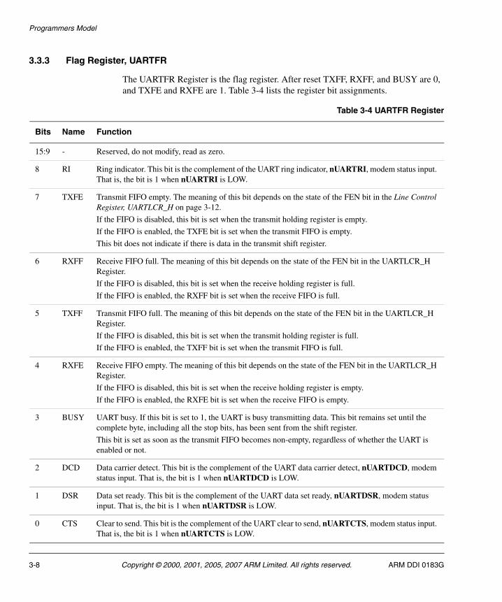
3.3.3 Flag Register, UARTFR
The UARTFR Register is the flag register. After reset TXFF, RXFF, and BUSY are 0, and TXFE and RXFE are 1. Table 3-4 lists the register bit assignments.
Table 3-4 UARTFR Register
Bits Name Function
15:9 - Reserved, do not modify, read as zero.
8 RI Ring indicator. This bit is the complement of the UART ring indicator, nUARTRI, modem status input. That is, the bit is 1 when nUARTRI is LOW.
7 TXFE Transmit FIFO empty. The meaning of this bit depends on the state of the FEN bit in the Line Control Register, UARTLCR_H on page 3-12.
If the FIFO is disabled, this bit is set when the transmit holding register is empty.
If the FIFO is enabled, the TXFE bit is set when the transmit FIFO is empty.
This bit does not indicate if there is data in the transmit shift register.
6 RXFF Receive FIFO full. The meaning of this bit depends on the state of the FEN bit in the UARTLCR_H Register.
If the FIFO is disabled, this bit is set when the receive holding register is full.
If the FIFO is enabled, the RXFF bit is set when the receive FIFO is full.
5 TXFF Transmit FIFO full. The meaning of this bit depends on the state of the FEN bit in the UARTLCR_H Register.
If the FIFO is disabled, this bit is set when the transmit holding register is full.
If the FIFO is enabled, the TXFF bit is set when the transmit FIFO is full.
4 RXFE Receive FIFO empty. The meaning of this bit depends on the state of the FEN bit in the UARTLCR_H Register.
If the FIFO is disabled, this bit is set when the receive holding register is empty.
If the FIFO is enabled, the RXFE bit is set when the receive FIFO is empty.
3 BUSY UART busy. If this bit is set to 1, the UART is busy transmitting data. This bit remains set until the complete byte, including all the stop bits, has been sent from the shift register.
This bit is set as soon as the transmit FIFO becomes non-empty, regardless of whether the UART is enabled or not.
2 DCD Data carrier detect. This bit is the complement of the UART data carrier detect, nUARTDCD, modem status input. That is, the bit is 1 when nUARTDCD is LOW.
1 DSR Data set ready. This bit is the complement of the UART data set ready, nUARTDSR, modem status input. That is, the bit is 1 when nUARTDSR is LOW.
0 CTS Clear to send. This bit is the complement of the UART clear to send, nUARTCTS, modem status input. That is, the bit is 1 when nUARTCTS is LOW.
3-8 Copyright © 2000, 2001, 2005, 2007 ARM Limited. All rights reserved. ARM DDI 0183G

Programmers Model
3.3.4 IrDA Low-Power Counter Register, UARTILPR
The UARTILPR Register is the IrDA low-power counter register. This is an 8-bit read/write register that stores the low-power counter divisor value used to generate the IrLPBaud16 signal by dividing down of UARTCLK. Table 3-5 lists the register bit assignments.
The IrLPBaud16 signal is generated by dividing down the UARTCLK signal according to the low-power divisor value written to the UARTILPR Register.
The low-power divisor value is calculated as follows:
• low-power divisor (ILPDVSR) = (FUARTCLK / FIrLPBaud16)
where FIrLPBaud16 is nominally 1.8432MHz.
You must select the divisor so that 1.42MHz < FIrLPBaud16 < 2.12MHz, results in a low-power pulse duration of 1.41-2.11µs (three times the period of IrLPBaud16).
Note In low-power IrDA mode the UART rejects random noise on the received serial data input by ignoring SIRIN pulses that are less than 3 periods of IrLPBaud16.
3.3.5 Integer Baud Rate Register, UARTIBRD
The UARTIBRD Register is the integer part of the baud rate divisor value. Table 3-6 lists the register bit assignments.
Table 3-5 UARTILPR Register
Bits Name Function
7:0 ILPDVSR 8-bit low-power divisor value.
These bits are cleared to 0 at reset.
Note Zero is an illegal value. Programming a zero value results in no IrLPBaud16 pulses being generated.
Table 3-6 UARTIBRD Register
Bits Name Function
15:0 BAUD DIVINT The integer baud rate divisor.
These bits are cleared to 0 on reset.
ARM DDI 0183G Copyright © 2000, 2001, 2005, 2007 ARM Limited. All rights reserved. 3-9

Programmers Model
3.3.6 Fractional Baud Rate Register, UARTFBRD
The UARTFBRD Register is the fractional part of the baud rate divisor value. Table 3-7 lists the register bit assignments.
The baud rate divisor is calculated as follows:
• Baud rate divisor BAUDDIV = (FUARTCLK/(16×Baud rate))
where FUARTCLK is the UART reference clock frequency.
The BAUDDIV is comprised of the integer value (BAUD DIVINT) and the fractional value (BAUD DIVFRAC).
Note • The contents of the UARTIBRD and UARTFBRD registers are not updated until
transmission or reception of the current character is complete.
• The minimum divide ratio possible is 1 and the maximum is 65535(216 - 1). That is, UARTIBRD = 0 is invalid and UARTFBRD is ignored when this is the case.
• Similarly, when UARTIBRD = 65535 (that is 0xFFFF), then UARTFBRD must not be greater than zero. If this is exceeded it results in an aborted transmission or reception.
Example 3-1 is an example of how to calculate the divisor value.
Example 3-1 Calculating the divisor value
If the required baud rate is 230400 and UARTCLK = 4MHz then:
Baud Rate Divisor = (4×10⁶)/(16×230400) = 1.085
This means BRDI = 1 and BRDF = 0.085.
Therefore, fractional part, m = integer((0.085×64)+0.5) = 5
Generated baud rate divider = 1+5/64 = 1.078
Table 3-7 UARTFBRD Register
Bits Name Function
5:0 BAUD DIVFRAC The fractional baud rate divisor.
These bits are cleared to 0 on reset.
3-10 Copyright © 2000, 2001, 2005, 2007 ARM Limited. All rights reserved. ARM DDI 0183G

Programmers Model
Generated baud rate = (4×10⁶)/(16×1.078) = 231911
Error = (231911-230400)/230400 × 100 = 0.656%
The maximum error using a 6-bit UARTFBRD Register = 1/64×100 = 1.56%. This occurs when m = 1, and the error is cumulative over 64 clock ticks.
Table 3-8 lists some typical bit rates and their corresponding divisors when UARTCLK is 7.3728MHz. These values do not use the fractional divider so the value in the UARTFBRD Register is zero.
Table 3-8 Typical baud rates and integer divisors when UARTCLK=7.3728MHz
Programmed integer divisor Bit rate (bps)
0x1 460800
0x2 230400
0x4 115200
0x6 76800
0x8 57600
0xC 38400
0x18 19200
0x20 14400
0x30 9600
0xC0 2400
0x180 1200
0x105D 110
ARM DDI 0183G Copyright © 2000, 2001, 2005, 2007 ARM Limited. All rights reserved. 3-11

Programmers Model
Table 3-9 lists some required bit rates and their corresponding integer and fractional divisor values and generated bit rates when UARTCLK is 4MHz.
3.3.7 Line Control Register, UARTLCR_H
The UARTLCR_H Register is the line control register. This register accesses bits 29 to 22 of the UART Line Control Register, UARTLCR.
Table 3-9 Integer and fractional divisors for typical baud rates when UARTCLK=4MHz
Programmedinteger divisor
Programmedfractional divisor
Requiredbit rate (bps)
Generatedbit rate (bps)
Error %
0x1 0x5 230400 231911 0.656
0x2 0xB 115200 115101 0.086
0x3 0x10 76800 76923 0.160
0x6 0x21 38400 38369 0.081
0x11 0x17 14400 14401 0.007
0x68 0xB 2400 2400 ~0
0x8E0 0x2F 110 110 ~0
3-12 Copyright © 2000, 2001, 2005, 2007 ARM Limited. All rights reserved. ARM DDI 0183G

Programmers Model
All the bits are cleared to 0 when reset. Table 3-10 lists the register bit assignments.
Table 3-10 UARTLCR_H Register
Bits Name Function
15:8 - Reserved, do not modify, read as zero.
7 SPS Stick parity select.
0 = stick parity is disabled
1 = either:
• if the EPS bit is 0 then the parity bit is transmitted and checked as a 1
• if the EPS bit is 1 then the parity bit is transmitted and checked as a 0.
This bit has no effect when the PEN bit disables parity checking and generation. See Table 3-11 on page 3-14 for the parity truth table.
6:5 WLEN Word length. These bits indicate the number of data bits transmitted or received in a frame as follows:
b11 = 8 bits
b10 = 7 bits
b01 = 6 bits
b00 = 5 bits.
4 FEN Enable FIFOs:
0 = FIFOs are disabled (character mode) that is, the FIFOs become 1-byte-deep holding registers
1 = transmit and receive FIFO buffers are enabled (FIFO mode).
3 STP2 Two stop bits select. If this bit is set to 1, two stop bits are transmitted at the end of the frame. The receive logic does not check for two stop bits being received.
2 EPS Even parity select. Controls the type of parity the UART uses during transmission and reception:
0 = odd parity. The UART generates or checks for an odd number of 1s in the data and parity bits.
1 = even parity. The UART generates or checks for an even number of 1s in the data and parity bits.
This bit has no effect when the PEN bit disables parity checking and generation. See Table 3-11 on page 3-14 for the parity truth table.
1 PEN Parity enable:
0 = parity is disabled and no parity bit added to the data frame
1 = parity checking and generation is enabled.
See Table 3-11 on page 3-14 for the parity truth table.
0 BRK Send break. If this bit is set to 1, a low-level is continually output on the UARTTXD output, after completing transmission of the current character. For the proper execution of the break command, the software must set this bit for at least two complete frames.
For normal use, this bit must be cleared to 0.
ARM DDI 0183G Copyright © 2000, 2001, 2005, 2007 ARM Limited. All rights reserved. 3-13

Programmers Model
The UARTLCR_H, UARTIBRD, and UARTFBRD registers form the single 30-bit wide UARTLCR Register that is updated on a single write strobe generated by a UARTLCR_H write. So, to internally update the contents of UARTIBRD or UARTFBRD, a UARTLCR_H write must always be performed at the end.
Note • To update the three registers there are two possible sequences:
— UARTIBRD write, UARTFBRD write, and UARTLCR_H write
— UARTFBRD write, UARTIBRD write, and UARTLCR_H write.
• To update UARTIBRD or UARTFBRD only:
— UARTIBRD write, or UARTFBRD write, and UARTLCR_H write.
Table 3-11 is a truth table for the Stick Parity Select (SPS), Even Parity Select (EPS), and Parity ENable (PEN) bits of the Line Control Register, UARTLCR_H on page 3-12.
Note • The UARTLCR_H, UARTIBRD, and UARTFBRD registers must not be
changed:
— when the UART is enabled
— when completing a transmission or a reception when it has been programmed to become disabled.
• The FIFO integrity is not guaranteed under the following conditions:
— after the BRK bit has been initiated
— if the software disables the UART in the middle of a transmission with data in the FIFO, and then re-enables it.
Table 3-11 Parity truth table
PEN EPS SPS Parity bit (transmitted or checked)
0 x x Not transmitted or checked
1 1 0 Even parity
1 0 0 Odd parity
1 0 1 1
1 1 1 0
3-14 Copyright © 2000, 2001, 2005, 2007 ARM Limited. All rights reserved. ARM DDI 0183G

Programmers Model
3.3.8 Control Register, UARTCR
The UARTCR Register is the control register. All the bits are cleared to 0 on reset except for bits 9 and 8 that are set to 1. Table 3-12 lists the register bit assignments.
Table 3-12 UARTCR Register
Bits Name Function
15 CTSEn CTS hardware flow control enable. If this bit is set to 1, CTS hardware flow control is enabled. Data is only transmitted when the nUARTCTS signal is asserted.
14 RTSEn RTS hardware flow control enable. If this bit is set to 1, RTS hardware flow control is enabled. Data is only requested when there is space in the receive FIFO for it to be received.
13 Out2 This bit is the complement of the UART Out2 (nUARTOut2) modem status output. That is, when the bit is programmed to a 1, the output is 0. For DTE this can be used as Ring Indicator (RI).
12 Out1 This bit is the complement of the UART Out1 (nUARTOut1) modem status output. That is, when the bit is programmed to a 1 the output is 0. For DTE this can be used as Data Carrier Detect (DCD).
11 RTS Request to send. This bit is the complement of the UART request to send, nUARTRTS, modem status output. That is, when the bit is programmed to a 1 then nUARTRTS is LOW.
10 DTR Data transmit ready. This bit is the complement of the UART data transmit ready, nUARTDTR, modem status output. That is, when the bit is programmed to a 1 then nUARTDTR is LOW.
9 RXE Receive enable. If this bit is set to 1, the receive section of the UART is enabled. Data reception occurs for either UART signals or SIR signals depending on the setting of the SIREN bit. When the UART is disabled in the middle of reception, it completes the current character before stopping.
8 TXE Transmit enable. If this bit is set to 1, the transmit section of the UART is enabled. Data transmission occurs for either UART signals, or SIR signals depending on the setting of the SIREN bit. When the UART is disabled in the middle of transmission, it completes the current character before stopping.
7 LBE Loopback enable. If this bit is set to 1 and the SIREN bit is set to 1 and the SIRTEST bit in the Test Control Register, UARTTCR on page 4-5 is set to 1, then the nSIROUT path is inverted, and fed through to the SIRIN path. The SIRTEST bit in the test register must be set to 1 to override the normal half-duplex SIR operation. This must be the requirement for accessing the test registers during normal operation, and SIRTEST must be cleared to 0 when loopback testing is finished. This feature reduces the amount of external coupling required during system test.
If this bit is set to 1, and the SIRTEST bit is set to 0, the UARTTXD path is fed through to the UARTRXD path.
In either SIR mode or UART mode, when this bit is set, the modem outputs are also fed through to the modem inputs.
This bit is cleared to 0 on reset, to disable loopback.
6:3 - Reserved, do not modify, read as zero.
ARM DDI 0183G Copyright © 2000, 2001, 2005, 2007 ARM Limited. All rights reserved. 3-15

Programmers Model
Note To enable transmission, the TXE bit and UARTEN bit must be set to 1. Similarly, to enable reception, the RXE bit and UARTEN bit, must be set to 1.
Note Program the control registers as follows:
1. Disable the UART.
2. Wait for the end of transmission or reception of the current character.
3. Flush the transmit FIFO by setting the FEN bit to 0 in the Line Control Register, UARTLCR_H on page 3-12.
4. Reprogram the UARTCR Register.
5. Enable the UART.
2 SIRLP SIR low-power IrDA mode. This bit selects the IrDA encoding mode. If this bit is cleared to 0, low-level bits are transmitted as an active high pulse with a width of 3/16th of the bit period. If this bit is set to 1, low-level bits are transmitted with a pulse width that is 3 times the period of the IrLPBaud16 input signal, regardless of the selected bit rate. Setting this bit uses less power, but might reduce transmission distances.
1 SIREN SIR enable:
0 = IrDA SIR ENDEC is disabled. nSIROUT remains LOW (no light pulse generated), and signal transitions on SIRIN have no effect.
1 = IrDA SIR ENDEC is enabled. Data is transmitted and received on nSIROUT and SIRIN. UARTTXD remains HIGH, in the marking state. Signal transitions on UARTRXD or modem status inputs have no effect.
This bit has no effect if the UARTEN bit disables the UART.
0 UARTEN UART enable:
0 = UART is disabled. If the UART is disabled in the middle of transmission or reception, it completes the current character before stopping.
1 = the UART is enabled. Data transmission and reception occurs for either UART signals or SIR signals depending on the setting of the SIREN bit.
Table 3-12 UARTCR Register (continued)
Bits Name Function
3-16 Copyright © 2000, 2001, 2005, 2007 ARM Limited. All rights reserved. ARM DDI 0183G

Programmers Model
3.3.9 Interrupt FIFO Level Select Register, UARTIFLS
The UARTIFLS Register is the interrupt FIFO level select register. You can use this register to define the FIFO level that triggers the assertion of UARTTXINTR and UARTRXINTR.
The interrupts are generated based on a transition through a level rather than being based on the level. That is, the interrupts are generated when the fill level progresses through the trigger level.
The bits are reset so that the trigger level is when the FIFOs are at the half-way mark. Table 3-13 lists the register bit assignments.
3.3.10 Interrupt Mask Set/Clear Register, UARTIMSC
The UARTIMSC Register is the interrupt mask set/clear register. It is a read/write register.
On a read this register returns the current value of the mask on the relevant interrupt. On a write of 1 to the particular bit, it sets the corresponding mask of that interrupt. A write of 0 clears the corresponding mask.
Table 3-13 UARTIFLS Register
Bits Name Function
15:6 - Reserved, do not modify, read as zero.
5:3 RXIFLSEL Receive interrupt FIFO level select. The trigger points for the receive interrupt are as follows:
b000 = Receive FIFO becomes ≥ 1/8 full
b001 = Receive FIFO becomes ≥ 1/4 full
b010 = Receive FIFO becomes ≥ 1/2 full
b011 = Receive FIFO becomes ≥ 3/4 full
b100 = Receive FIFO becomes ≥ 7/8 full
b101-b111 = reserved.
2:0 TXIFLSEL Transmit interrupt FIFO level select. The trigger points for the transmit interrupt are as follows:
b000 = Transmit FIFO becomes ≤ 1/8 full
b001 = Transmit FIFO becomes ≤ 1/4 full
b010 = Transmit FIFO becomes ≤ 1/2 full
b011 = Transmit FIFO becomes ≤ 3/4 full
b100 = Transmit FIFO becomes ≤ 7/8 full
b101-b111 = reserved.
ARM DDI 0183G Copyright © 2000, 2001, 2005, 2007 ARM Limited. All rights reserved. 3-17

Programmers Model
All the bits are cleared to 0 when reset. Table 3-14 lists the register bit assignments.
Table 3-14 UARTIMSC Register
Bits Name Function
15:11 - Reserved, read as zero, do not modify.
10 OEIM Overrun error interrupt mask. A read returns the current mask for the UARTOEINTR interrupt.
On a write of 1, the mask of the UARTOEINTR interrupt is set. A write of 0 clears the mask.
9 BEIM Break error interrupt mask. A read returns the current mask for the UARTBEINTR interrupt.
On a write of 1, the mask of the UARTBEINTR interrupt is set. A write of 0 clears the mask.
8 PEIM Parity error interrupt mask. A read returns the current mask for the UARTPEINTR interrupt.
On a write of 1, the mask of the UARTPEINTR interrupt is set. A write of 0 clears the mask.
7 FEIM Framing error interrupt mask. A read returns the current mask for the UARTFEINTR interrupt.
On a write of 1, the mask of the UARTFEINTR interrupt is set. A write of 0 clears the mask.
6 RTIM Receive timeout interrupt mask. A read returns the current mask for the UARTRTINTR interrupt.
On a write of 1, the mask of the UARTRTINTR interrupt is set. A write of 0 clears the mask.
5 TXIM Transmit interrupt mask. A read returns the current mask for the UARTTXINTR interrupt.
On a write of 1, the mask of the UARTTXINTR interrupt is set. A write of 0 clears the mask.
4 RXIM Receive interrupt mask. A read returns the current mask for the UARTRXINTR interrupt.
On a write of 1, the mask of the UARTRXINTR interrupt is set. A write of 0 clears the mask.
3 DSRMIM nUARTDSR modem interrupt mask. A read returns the current mask for the UARTDSRINTR interrupt.
On a write of 1, the mask of the UARTDSRINTR interrupt is set. A write of 0 clears the mask.
2 DCDMIM nUARTDCD modem interrupt mask. A read returns the current mask for the UARTDCDINTR interrupt.
On a write of 1, the mask of the UARTDCDINTR interrupt is set. A write of 0 clears the mask.
1 CTSMIM nUARTCTS modem interrupt mask. A read returns the current mask for the UARTCTSINTR interrupt.
On a write of 1, the mask of the UARTCTSINTR interrupt is set. A write of 0 clears the mask.
0 RIMIM nUARTRI modem interrupt mask. A read returns the current mask for the UARTRIINTR interrupt.
On a write of 1, the mask of the UARTRIINTR interrupt is set. A write of 0 clears the mask.
3-18 Copyright © 2000, 2001, 2005, 2007 ARM Limited. All rights reserved. ARM DDI 0183G

Programmers Model
3.3.11 Raw Interrupt Status Register, UARTRIS
The UARTRIS Register is the raw interrupt status register. It is a read-only register. This register returns the current raw status value, prior to masking, of the corresponding interrupt. A write has no effect.
Caution All the bits, except for the modem status interrupt bits (bits 3 to 0), are cleared to 0 when reset. The modem status interrupt bits are undefined after reset.
Table 3-15 lists the register bit assignments.
Table 3-15 UARTRIS Register
Bits Name Function
15:11 - Reserved, read as zero, do not modify.
10 OERIS Overrun error interrupt status. Returns the raw interrupt state of the UARTOEINTR interrupt.
9 BERIS Break error interrupt status. Returns the raw interrupt state of the UARTBEINTR interrupt.
8 PERIS Parity error interrupt status. Returns the raw interrupt state of the UARTPEINTR interrupt.
7 FERIS Framing error interrupt status. Returns the raw interrupt state of the UARTFEINTR interrupt.
6 RTRIS Receive timeout interrupt status. Returns the raw interrupt state of the UARTRTINTR interrupt.a
5 TXRIS Transmit interrupt status. Returns the raw interrupt state of the UARTTXINTR interrupt.
4 RXRIS Receive interrupt status. Returns the raw interrupt state of the UARTRXINTR interrupt.
3 DSRRMIS nUARTDSR modem interrupt status. Returns the raw interrupt state of the UARTDSRINTR interrupt.
2 DCDRMIS nUARTDCD modem interrupt status. Returns the raw interrupt state of the UARTDCDINTR interrupt.
1 CTSRMIS nUARTCTS modem interrupt status. Returns the raw interrupt state of the UARTCTSINTR interrupt.
0 RIRMIS nUARTRI modem interrupt status. Returns the raw interrupt state of the UARTRIINTR interrupt.
a. In this case the raw interrupt cannot be set unless the mask is set, this is because the mask acts as an enable for power saving. That is, the same status can be read from UARTMIS and UARTRIS for the receive timeout interrupt.
ARM DDI 0183G Copyright © 2000, 2001, 2005, 2007 ARM Limited. All rights reserved. 3-19

Programmers Model
3.3.12 Masked Interrupt Status Register, UARTMIS
The UARTMIS Register is the masked interrupt status register. It is a read-only register. This register returns the current masked status value of the corresponding interrupt. A write has no effect.
All the bits except for the modem status interrupt bits (bits 3 to 0) are cleared to 0 when reset. The modem status interrupt bits are undefined after reset. Table 3-16 lists the register bit assignments.
Table 3-16 UARTMIS Register
Bits Name Function
15:11 - Reserved, read as zero, do not modify
10 OEMIS Overrun error masked interrupt status. Returns the masked interrupt state of the UARTOEINTR interrupt.
9 BEMIS Break error masked interrupt status. Returns the masked interrupt state of the UARTBEINTR interrupt.
8 PEMIS Parity error masked interrupt status. Returns the masked interrupt state of the UARTPEINTR interrupt.
7 FEMIS Framing error masked interrupt status. Returns the masked interrupt state of the UARTFEINTR interrupt.
6 RTMIS Receive timeout masked interrupt status. Returns the masked interrupt state of the UARTRTINTR interrupt.
5 TXMIS Transmit masked interrupt status. Returns the masked interrupt state of the UARTTXINTR interrupt.
4 RXMIS Receive masked interrupt status. Returns the masked interrupt state of the UARTRXINTR interrupt.
3 DSRMMIS nUARTDSR modem masked interrupt status. Returns the masked interrupt state of the UARTDSRINTR interrupt.
2 DCDMMIS nUARTDCD modem masked interrupt status. Returns the masked interrupt state of the UARTDCDINTR interrupt.
1 CTSMMIS nUARTCTS modem masked interrupt status. Returns the masked interrupt state of the UARTCTSINTR interrupt.
0 RIMMIS nUARTRI modem masked interrupt status. Returns the masked interrupt state of the UARTRIINTR interrupt.
3-20 Copyright © 2000, 2001, 2005, 2007 ARM Limited. All rights reserved. ARM DDI 0183G
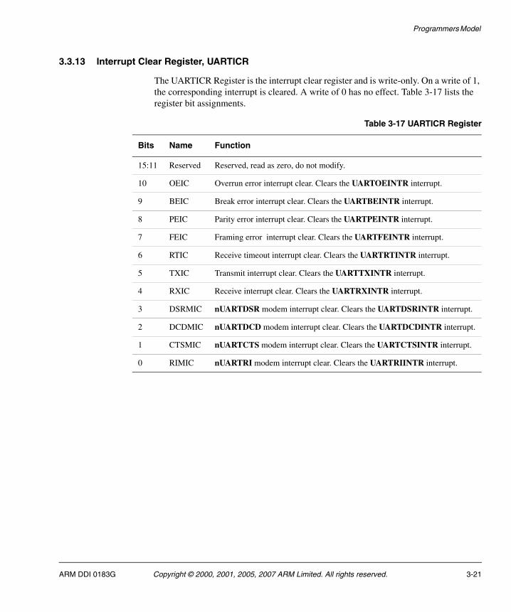
Programmers Model
3.3.13 Interrupt Clear Register, UARTICR
The UARTICR Register is the interrupt clear register and is write-only. On a write of 1, the corresponding interrupt is cleared. A write of 0 has no effect. Table 3-17 lists the register bit assignments.
Table 3-17 UARTICR Register
Bits Name Function
15:11 Reserved Reserved, read as zero, do not modify.
10 OEIC Overrun error interrupt clear. Clears the UARTOEINTR interrupt.
9 BEIC Break error interrupt clear. Clears the UARTBEINTR interrupt.
8 PEIC Parity error interrupt clear. Clears the UARTPEINTR interrupt.
7 FEIC Framing error interrupt clear. Clears the UARTFEINTR interrupt.
6 RTIC Receive timeout interrupt clear. Clears the UARTRTINTR interrupt.
5 TXIC Transmit interrupt clear. Clears the UARTTXINTR interrupt.
4 RXIC Receive interrupt clear. Clears the UARTRXINTR interrupt.
3 DSRMIC nUARTDSR modem interrupt clear. Clears the UARTDSRINTR interrupt.
2 DCDMIC nUARTDCD modem interrupt clear. Clears the UARTDCDINTR interrupt.
1 CTSMIC nUARTCTS modem interrupt clear. Clears the UARTCTSINTR interrupt.
0 RIMIC nUARTRI modem interrupt clear. Clears the UARTRIINTR interrupt.
ARM DDI 0183G Copyright © 2000, 2001, 2005, 2007 ARM Limited. All rights reserved. 3-21
Programmers Model
3.3.14 DMA Control Register, UARTDMACR
The UARTDMACR Register is the DMA control register. It is a read/write register. All the bits are cleared to 0 on reset. Table 3-18 lists the register bit assignments.
3.3.15 Peripheral Identification Registers, UARTPeriphID0-3
The UARTPeriphID0-3 Registers are four 8-bit registers, that span address locations 0xFE0 - 0xFEC. The registers can conceptually be treated as a 32-bit register. The read only registers provide the following options of the peripheral:
PartNumber[11:0] Identifies the peripheral. This is 0x011 for the UART.
Designer ID[19:12] Identifies the designer. This is set to 0x41, to indicate that ARM designed the peripheral.
Revision[23:20] The peripheral revision number is revision-dependent. See Table 3-21 on page 3-24.
Configuration[31:24]
The configuration option of the peripheral. The configuration value is 0.
Figure 3-1 on page 3-23 shows the bit assignment for the UARTPeriphID0-3 Registers.
Table 3-18 UARTDMACR Register
Bits Name Function
15:3 - Reserved, read as zero, do not modify.
2 DMAONERR DMA on error. If this bit is set to 1, the DMA receive request outputs, UARTRXDMASREQ or UARTRXDMABREQ, are disabled when the UART error interrupt is asserted.
1 TXDMAE Transmit DMA enable. If this bit is set to 1, DMA for the transmit FIFO is enabled.
0 RXDMAE Receive DMA enable. If this bit is set to 1, DMA for the receive FIFO is enabled.
3-22 Copyright © 2000, 2001, 2005, 2007 ARM Limited. All rights reserved. ARM DDI 0183G

Programmers Model
Figure 3-1 Peripheral Identification Register bit assignments
Note When you design a systems memory map you must remember that the register has a 4KB memory footprint. All memory accesses to the Peripheral Identification Registers must be 32-bit, using the LDR and STR instructions.
The four, 8-bit Peripheral Identification Registers are described in the following subsections:
• UARTPeriphID0 Register
• UARTPeriphID1 Register on page 3-24
• UARTPeriphID2 Register on page 3-24
• UARTPeriphID3 Register on page 3-25.
UARTPeriphID0 Register
The UARTPeriphID0 Register is hard coded and the fields in the register determine the reset value. Table 3-19 lists the register bit assignments.
Table 3-19 UARTPeriphID0 Register
Bits Name Description
15:8 - Reserved, read undefined must read as zeros
7:0 PartNumber0 These bits read back as 0x11
ARM DDI 0183G Copyright © 2000, 2001, 2005, 2007 ARM Limited. All rights reserved. 3-23

Programmers Model
UARTPeriphID1 Register
The UARTPeriphID1 Register is hard coded and the fields in the register determine the reset value. Table 3-20 lists the register bit assignments.
UARTPeriphID2 Register
The UARTPeriphID2 Register is hard coded and the fields in the register determine the reset value. Table 3-21 lists the register bit assignments.
Table 3-20 UARTPeriphID1 Register
Bits Name Description
15:8 - Reserved, read undefined, must read as zeros
7:4 Designer0 These bits read back as 0x1
3:0 PartNumber1 These bits read back as 0x0
Table 3-21 UARTPeriphID2 Register
Bits Name Description
15:8 - Reserved, read undefined, must read as zeros
7:4 Revision This field depends on the revision of the UART:
r1p0 0x0
r1p1 0x1
r1p3 0x2
r1p4 0x2
r1p5 0x3
3:0 Designer1 These bits read back as 0x4
3-24 Copyright © 2000, 2001, 2005, 2007 ARM Limited. All rights reserved. ARM DDI 0183G

Programmers Model
UARTPeriphID3 Register
The UARTPeriphID3 Register is hard coded and the fields in the register determine the reset value. Table 3-22 lists the register bit assignments.
3.3.16 PrimeCell Identification Registers, UARTPCellID0-3
The UARTPCellID0-3 Registers are four 8-bit wide registers, that span address locations 0xFF0-0xFFC. The registers can conceptually be treated as a 32-bit register. The register is used as a standard cross-peripheral identification system. The UARTPCellID Register is set to 0xB105F00D. Figure 3-2 shows the bit assignment for the UARTPCellID0-3 Registers.
Figure 3-2 PrimeCell Identification Register bit assignments
The four, 8-bit PrimeCell Identification Registers are described in the following subsections:
• UARTPCellID0 Register on page 3-26
• UARTPCellID1 Register on page 3-26
• UARTPCellID2 Register on page 3-26
• UARTPCellID3 Register on page 3-27.
Table 3-22 UARTPeriphID3 Register
Bits Name Description
15:8 - Reserved, read undefined, must read as zeros
7:0 Configuration These bits read back as 0x00
ARM DDI 0183G Copyright © 2000, 2001, 2005, 2007 ARM Limited. All rights reserved. 3-25

Programmers Model
UARTPCellID0 Register
The UARTPCellID0 Register is hard coded and the fields in the register determine the reset value. Table 3-23 lists the register bit assignments.
UARTPCellID1 Register
The UARTPCellID1 Register is hard coded and the fields in the register determine the reset value. Table 3-24 lists the register bit assignments.
UARTPCellID2 Register
The UARTPCellID2 Register is hard coded and the fields in the register determine the reset value. Table 3-25 lists the register bit assignments.
Table 3-23 UARTPCellID0 Register
Bits Name Description
15:8 - Reserved, read undefined, must read as zeros
7:0 UARTPCellID0 These bits read back as 0x0D
Table 3-24 UARTPCellID1 Register
Bits Name Description
15:8 - Reserved, read undefined, must read as zeros
7:0 UARTPCellID1 These bits read back as 0xF0
Table 3-25 UARTPCellID2 Register
Bits Name Description
15:8 - Reserved, read undefined, must read as zeros
7:0 UARTPCellID2 These bits read back as 0x05
3-26 Copyright © 2000, 2001, 2005, 2007 ARM Limited. All rights reserved. ARM DDI 0183G

Programmers Model
UARTPCellID3 Register
The UARTPCellID3 Register is hard coded and the fields in the register determine the reset value. Table 3-26 lists the register bit assignments.
Table 3-26 UARTPCellID3 Register
Bits Name Description
15:8 - Reserved, read undefined, must read as zeros
7:0 UARTPCellID3 These bits read back as 0xB1
ARM DDI 0183G Copyright © 2000, 2001, 2005, 2007 ARM Limited. All rights reserved. 3-27

Programmers Model
3-28 Copyright © 2000, 2001, 2005, 2007 ARM Limited. All rights reserved. ARM DDI 0183G

Chapter 4 Programmers Model for Test
This chapter describes the additional logic for integration testing. It contains the following sections:
• Test harness overview on page 4-2
• Scan testing on page 4-3
• Summary of test registers on page 4-4
• Test register descriptions on page 4-5
• Integration testing of block inputs on page 4-9
• Integration testing of block outputs on page 4-11
• Integration test summary on page 4-14.
ARM DDI 0183G Copyright © 2000, 2001, 2005, 2007 ARM Limited. All rights reserved. 4-1

Programmers Model for Test
4.1 Test harness overview
The additional logic for functional verification and integration vectors enables:
• capture of input signals to the block
• stimulation of the output signals.
The integration vectors provide a way of verifying that the UART is correctly wired into a system. This is done by separately testing three groups of signals:
AMBA signals
These are tested by checking the connections of all the address and data bits.
Primary input/output signals
These are tested using a simple trickbox that can demonstrate the correct connection of the input/output signals to external pads.
Intra-chip signals (such as interrupt sources)
The tests for these signals are system-specific, and enable you to write the necessary tests. Additional logic is implemented enabling you to read and write to each intra-chip input/output signal.
These test features are controlled by test registers. This enables you to test the UART in isolation from the rest of the system using only transfers from the AMBA APB.
Off-chip test vectors are supplied using a 32-bit parallel External Bus Interface (EBI) and converted to internal AMBA bus transfers. The application of test vectors is controlled through the Test Interface Controller (TIC) AMBA bus master module.
4-2 Copyright © 2000, 2001, 2005, 2007 ARM Limited. All rights reserved. ARM DDI 0183G

Programmers Model for Test
4.2 Scan testing
The UART has been designed to simplify:
• insertion of scan test cells
• use of Automatic Test Pattern Generation (ATPG).
This provides an alternative method of manufacturing test.
ARM DDI 0183G Copyright © 2000, 2001, 2005, 2007 ARM Limited. All rights reserved. 4-3

Programmers Model for Test
4.3 Summary of test registers
Table 4-1 lists the UART test registers.
Table 4-1 Test registers summary
Offset Name Type Reset Width Description
0x080 UARTTCR RW 0x0 3 Test Control Register, UARTTCR on page 4-5
0x084 UARTITIP RW 0x00 8 Integration Test Input Register, UARTITIP on page 4-6
0x088 UARTITOP RW 0x000 14 Integration Test Output Register, UARTITOP on page 4-7
0x08C UARTTDR RW 0x--- 11 Test Data Register, UARTTDR on page 4-8
4-4 Copyright © 2000, 2001, 2005, 2007 ARM Limited. All rights reserved. ARM DDI 0183G

Programmers Model for Test
4.4 Test register descriptions
This section describes the UART test registers and Table 4-1 on page 4-4 lists the cross references to individual registers.
4.4.1 Test Control Register, UARTTCR
UARTTCR is the test control register. This general test register controls operation of the UART under test conditions. Table 4-2 lists the register bit assignments.
Table 4-2 UARTTCR register
Bits Name Function
16:3 - Reserved, unpredictable when read.
2 SIRTEST SIR test enable. Setting this bit to 1 enables the receive data path during IrDA transmission (SIR full-duplex operation is only available when testing). This bit must be set to 1 to enable SIR system loopback testing, and you must also set the LBE bit to 1 in the Control Register, UARTCR on page 3-15.
Clearing this bit to 0 disables the receive logic when the SIR is transmitting (normal operation).
This bit defaults to 0 for normal operation (half-duplex operation).
1 TESTFIFO Test FIFO enable. When this bit it 1, a write to the Test Data Register, UARTTDR on page 4-8 writes data into the receive FIFO, and reads from the UARTTDR register reads data out of the transmit FIFO.
When this bit is 0, data cannot be read directly from the transmit FIFO or written directly to the receive FIFO (normal operation).
The reset value is 0.
0 ITEN Integration test enable. When this bit is 1, the UART is placed in integration test mode, otherwise it is in normal operation.
ARM DDI 0183G Copyright © 2000, 2001, 2005, 2007 ARM Limited. All rights reserved. 4-5

Programmers Model for Test
4.4.2 Integration Test Input Register, UARTITIP
UARTITIP is the integration test input read/set register. It is a a read/write register. In integration test mode it enables inputs to be both written to and read from. Table 4-3 lists the register bit assignments.
Table 4-3 UARTITIP register
Bits Name Function
16:8 - Reserved, unpredictable when read.
7 UARTTXDMACLR Writes to this bit specify the value to be driven on the intra-chip input, UARTTXDMACLR, in the integration test mode.
Reads return the value of UARTTXDMACLR at the output of the test multiplexor.
6 UARTRXDMACLR Writes to this bit specify the value to be driven on the intra-chip input, UARTRXDMACLR, in the integration test mode.
Reads return the value of UARTRXDMACLR at the output of the test multiplexor.
5 nUARTRI Reads return the value of the nUARTRI primary input.
4 nUARTDCD Reads return the value of the nUARTDCD primary input.
3 nUARTCTS Reads return the value of the nUARTCTS primary input.
2 nUARTDSR Reads return the value of the nUARTDSR primary input.
1 SIRIN Reads return the value of the SIRIN primary input.
0 UARTRXD Reads return the value of the UARTRXD primary input.
4-6 Copyright © 2000, 2001, 2005, 2007 ARM Limited. All rights reserved. ARM DDI 0183G

Programmers Model for Test
4.4.3 Integration Test Output Register, UARTITOP
UARTITOP is the integration test output read/set register. The primary outputs are read only and the intra-chip outputs are read/write. In integration test mode it enables outputs to be both written to and read from. Table 4-4 lists the register bit assignments.
Table 4-4 UARTITOP register
Bits Name Function
15 UARTTXDMASREQ Intra-chip output. Writes specify the value to be driven on UARTTXDMASREQ.
Reads return the value of UARTTXDMASREQ at the output of the test multiplexor.
14 UARTTXDMABREQ Intra-chip output. Writes specify the value to be driven on UARTTXDMABREQ.
Reads return the value of UARTTXDMABREQ at the output of the test multiplexor.
13 UARTRXDMASREQ Intra-chip output. Writes specify the value to be driven on UARTRXDMASREQ.
Reads return the value of UARTRXDMASREQ at the output of the test multiplexor.
12 UARTRXDMABREQ Intra-chip output. Writes specify the value to be driven on UARTDMABREQ.
Reads return the value of UARTDMABREQ at the output of the test multiplexor.
11 UARTMSINTR Intra-chip output. Writes specify the value to be driven on UARTMSINTR.
Reads return the value of UARTMSINTR at the output of the test multiplexor.
10 UARTRXINTR Intra-chip output. Writes specify the value to be driven on UARTRXINTR.
Reads return the value of UARTRXINTR at the output of the test multiplexor.
9 UARTTXINTR Intra-chip output. Writes specify the value to be driven on UARTTXINTR.
Reads return the value of UARTTXINTR at the output of the test multiplexor.
8 UARTRTINTR Intra-chip output. Writes specify the value to be driven on UARTRTINTR.
Reads return the value of UARTRTINTR at the output of the test multiplexor.
7 UARTEINTR Intra-chip output. Writes specify the value to be driven on UARTEINTR.
Reads return the value of UARTEINTR at the output of the test multiplexor.
6 UARTINTR Intra-chip output. Writes specify the value to be driven on UARTINTR.
Reads return the value of UARTINTR at the output of the test multiplexor.
5 nUARTOut2 Primary output. Writes specify the value to be driven on nUARTOut2.
4 nUARTOut1 Primary output. Writes specify the value to be driven on nUARTOut1.
3 nUARTRTS Primary output. Writes specify the value to be driven on nUARTRTS.
ARM DDI 0183G Copyright © 2000, 2001, 2005, 2007 ARM Limited. All rights reserved. 4-7

Programmers Model for Test
4.4.4 Test Data Register, UARTTDR
UARTTDR is the test data register. It enables data to be written into the receive FIFO and read out from the transmit FIFO for test purposes. This test function is enabled by the TESTFIFO bit in the Test Control Register, UARTTCR on page 4-5. Table 4-5 lists the register bit assignments.
2 nUARTDTR Primary output. Writes specify the value to be driven on nUARTDTR.
1 nSIROUT Primary output. Writes specify the value to be driven on nSIROUT.
0 UARTTXD Primary output. Writes specify the value to be driven on UARTTXD.
Table 4-4 UARTITOP register (continued)
Bits Name Function
Table 4-5 UARTTDR register
Bits Name Function
16:11 - Reserved, unpredictable when read
10:0 DATA When the TESTFIFO bit is set to 1, data is written into the receive FIFO and read out of the transmit FIFO
4-8 Copyright © 2000, 2001, 2005, 2007 ARM Limited. All rights reserved. ARM DDI 0183G

Programmers Model for Test
4.5 Integration testing of block inputs
The following sections describe the integration testing for the block inputs:
• Intra-chip inputs
• Primary inputs on page 4-10.
4.5.1 Intra-chip inputs
Figure 4-1 shows the implementation of the input integration test harness. The ITEN bit in the Test Control Register, UARTTCR on page 4-5 controls the multiplexor, that is used in the read path of the UARTTXDMACLR and UARTRXDMACLR intra-chip inputs. If the ITEN bit is deasserted, the UARTTXDMACLR and UARTRXDMACLR intra-chip inputs are routed as the internal UARTTXDMACLR and UARTRXDMACLR inputs respectively, otherwise the stored register values are driven on the internal line. All other read-only bits in the Integration Test Input Register, UARTITIP on page 4-6 are connected directly to the primary input pins.
Figure 4-1 Input integration test harness
When you run integration tests with the UART in a standalone test setup:
• Write a 1 to the ITEN bit in the Test Control Register, UARTTCR on page 4-5. This selects the test path from the UARTITIP[7:6] register bits to the UARTRXDMACLR and UARTTXDMACLR signals.
ARM DDI 0183G Copyright © 2000, 2001, 2005, 2007 ARM Limited. All rights reserved. 4-9

Programmers Model for Test
• Write a 1 and then a 0 to each of the UARTITIP[7:6] register bits, and read the same register bits to ensure that the value written is read out.
When you run integration tests with the UART as part of an integrated system:
• Write a 0 to the ITEN bit in the Test Control Register, UARTTCR on page 4-5. This selects the normal path from the external UARTRXDMACLR pin to the internal UARTRXDMACLR signal, and the path from the external UARTTXDMACLR pin to the internal UARTTXDMACLR pin.
• Write a 1 and then a 0 to the internal test registers of the DMA controller to toggle the UARTRXDMACLR signal connection between the DMA controller and the UART. Read the UARTRXDMACLR bit in the Integration Test Input Register, UARTITIP on page 4-6 to verify that the value written into the DMA controller, is read out through the UART.
Similarly, write a 1 and then a 0 to the internal registers of the DMA controller to toggle the UARTTXDMACLR signal connection between the DMA controller and the UART. Read the UARTTXDMACLR bit in the Integration Test Input Register, UARTITIP on page 4-6 to verify that the value written into the DMA controller, is read out through the UART.
4.5.2 Primary inputs
The primary inputs are tested using the integration vector trickbox by looping back primary outputs as follows:
• UARTTXD to UARTRXD• nSIROUT to SIRIN• nUARTRTS to nUARTCTS• nUARTOUT1 to nUARTDCD• nUARTDTR to nUARTDSR• nUARTOUT2 to nUARTRI.
Write a 1 to the ITEN bit in the Test Control Register, UARTTCR on page 4-5. Using the Integration Test Output Register, UARTITOP on page 4-7 program bits [5:0] to drive HIGHs and LOWs on the primary output signals and read back the status using bits [5:0] in the Integration Test Input Register, UARTITIP on page 4-6.
4-10 Copyright © 2000, 2001, 2005, 2007 ARM Limited. All rights reserved. ARM DDI 0183G

Programmers Model for Test
4.6 Integration testing of block outputs
The following sections describe the integration testing for the block outputs:
• Intra-chip outputs
• Primary outputs on page 4-12.
4.6.1 Intra-chip outputs
Use this test for the following outputs:
• UARTTXDMASREQ• UARTTXDMABREQ• UARTRXDMASREQ• UARTRXDMABREQ• UARTINTR• UARTMSINTR• UARTRXINTR• UARTTXINTR• UARTRTINTR• UARTEINTR.
When you run integration tests with the UART in a standalone test setup:
• Write a 1 to the ITEN bit in the Test Control Register, UARTTCR on page 4-5. This selects the test path from the UARTITOP0[15:6] register bits to the intra-chip output signals.
• Write a 1 and then a 0 to the UARTITOP0[15:6] register bits, and read the same register bits to verify that the value written is read out.
When you run integration tests with the UART as part of an integrated system:
• Write a 1 to the ITEN bit in the Test Control Register, UARTTCR on page 4-5. This selects the test path from the UARTITOP0[15:6] register bits to the intra-chip output signals.
• Write a 1 and then a 0 to the UARTITOP0[15:6] register bits to toggle the signal connections between the DMA controller/interrupt controller and the UART. Read from the internal test registers of the DMA controller/interrupt controller to verify that the value written into the UARTITOP0[15:6] register bits is read out through the UART.
Figure 4-2 on page 4-12 shows the implementation of the output integration test harness for intra-chip outputs.
ARM DDI 0183G Copyright © 2000, 2001, 2005, 2007 ARM Limited. All rights reserved. 4-11
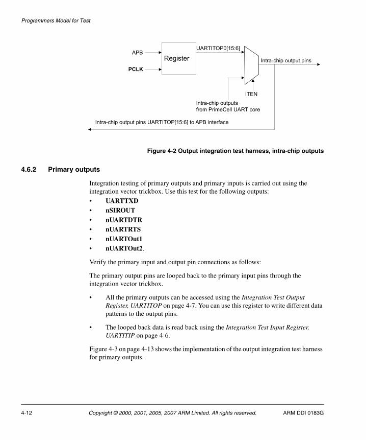
Programmers Model for Test
Figure 4-2 Output integration test harness, intra-chip outputs
4.6.2 Primary outputs
Integration testing of primary outputs and primary inputs is carried out using the integration vector trickbox. Use this test for the following outputs:
• UARTTXD• nSIROUT• nUARTDTR• nUARTRTS• nUARTOut1• nUARTOut2.
Verify the primary input and output pin connections as follows:
The primary output pins are looped back to the primary input pins through the integration vector trickbox.
• All the primary outputs can be accessed using the Integration Test Output Register, UARTITOP on page 4-7. You can use this register to write different data patterns to the output pins.
• The looped back data is read back using the Integration Test Input Register, UARTITIP on page 4-6.
Figure 4-3 on page 4-13 shows the implementation of the output integration test harness for primary outputs.
4-12 Copyright © 2000, 2001, 2005, 2007 ARM Limited. All rights reserved. ARM DDI 0183G

Programmers Model for Test
Figure 4-3 Output integration test harness, primary outputs
ARM DDI 0183G Copyright © 2000, 2001, 2005, 2007 ARM Limited. All rights reserved. 4-13

Programmers Model for Test
4.7 Integration test summary
Table 4-6 lists the integration test strategy for all UART pins.
Table 4-6 Integration test strategy
Name TypeSource/destination
Test strategy
PRESETn Input Reset controller Not tested using integration test vectors
PADDR[11:2] Input
APB Register read/write
PCLK Input
PENABLE Input
PRDATA[15:0] Output
PSEL Input
PWDATA[15:0] Input
PWRITE Input
UARTCLK Input Clock generatorNot tested using integration test vectors
nUARTRST Input Reset controller
UARTMSINTR Output Interrupt controller
Use Integration Test Output Register, UARTITOP on page 4-7
UARTRXINTR Output Interrupt controller
UARTTXINTR Output Interrupt controller
UARTRTINTR Output Interrupt controller
UARTEINTR Output Interrupt controller
UARTTXDMASREQ Output DMA controller
UARTRXDMASREQ Output DMA controller
UARTTXDMABREQ Output DMA controller
UARTRXDMABREQ Output DMA controller
UARTTXDMACLR Input DMA controllerUse Integration Test Input Register, UARTITIP on page 4-6
UARTRXDMACLR Input DMA controller
4-14 Copyright © 2000, 2001, 2005, 2007 ARM Limited. All rights reserved. ARM DDI 0183G

Programmers Model for Test
UARTINTR Output Interrupt controller Use Integration Test Output Register, UARTITOP on page 4-7
SCANENABLE Input Test controller
Not tested using integration test vectors
SCANINPCLK Input Test controller
SCANINUCLK Input Test controller
SCANOUTPCLK Output Test controller
SCANOUTUCLK Output Test controller
nUARTCTS Input
PAD
Use the integration vector trickbox with:
• Integration Test Input Register, UARTITIP on page 4-6
• Integration Test Output Register, UARTITOP on page 4-7
nUARTDCD Input
nUARTDSR Input
nUARTRI Input
UARTRXD Input
SIRIN Input
UARTTXD Output
nSIROUT Output
nUARTDTR Output
nUARTRTS Output
nUARTOut1 Output
nUARTOut2 Output
Table 4-6 Integration test strategy (continued)
Name TypeSource/destination
Test strategy
ARM DDI 0183G Copyright © 2000, 2001, 2005, 2007 ARM Limited. All rights reserved. 4-15

Programmers Model for Test
4-16 Copyright © 2000, 2001, 2005, 2007 ARM Limited. All rights reserved. ARM DDI 0183G

Appendix A Signal Descriptions
This appendix describes the signals that interface with the UART block. It contains the following sections:
• AMBA APB signals on page A-2
• On-chip signals on page A-3
• Signals to pads on page A-5.
ARM DDI 0183G Copyright © 2000, 2001, 2005, 2007 ARM Limited. All rights reserved. A-1

Signal Descriptions
A.1 AMBA APB signals
Table A-1 lists the signals that the APB slave interface provides.
See the AMBA Specification (Rev 2.0) for more information about the APB signals.
Table A-1 APB slave interface signals
Name TypeSource/destination
Description
PRESETn Input Reset controller Bus reset signal, active LOW.
PADDR[11:2] Input APB Subset of AMBA APB address bus.
PCLK Input APB APB clock, used to time all bus transfers.
PENABLE Input APB APB enable signal. PENABLE is asserted HIGH for one cycle of PCLK to enable a bus transfer.
PRDATA[15:0] Output APB Subset of unidirectional AMBA APB read data bus.
PSEL Input APB UART and SIR ENDEC select signal from decoder. When set HIGH this signal indicates the slave device is selected by the AMBA APB bridge, and that a data transfer is required.
PWDATA[15:0] Input APB Subset of unidirectional AMBA APB write data bus.
PWRITE Input APB APB transfer direction signal, indicates a write access when HIGH, read access when LOW.
A-2 Copyright © 2000, 2001, 2005, 2007 ARM Limited. All rights reserved. ARM DDI 0183G

Signal Descriptions
A.2 On-chip signals
A free-running reference clock, UARTCLK, must be provided. By default it is assumed to be asynchronous to PCLK. The UARTCLK clock must have a frequency between 1.42MHz to 542.72MHz to ensure that the low-power IrDA mode transmit pulse duration complies with the IrDA SIR specification.
The reset inputs are asynchronously asserted but synchronously removed for each of the clock domains in the UART. This ensures that logic is reset even if clocks are not present, to avoid any static power consumption problems at power up. Each clock domain has a individual reset to simplify the process of inserting scan test cells.
Table A-2 lists the on-chip signals that the UART provides.
Table A-2 On-chip signals
Name TypeSource/destination
Description
UARTCLK Input Clock generator UART reference clock.
nUARTRST Input Reset controller UART reset signal to UARTCLK clock domain, active LOW. The reset controller must use PRESETn to assert nUARTRST asynchronously but negate it synchronously with UARTCLK.
UARTMSINTR Output Interrupt controller UART modem status interrupt, active HIGH.
UARTRXINTR Output Interrupt controller UART receive FIFO interrupt, active HIGH.
UARTTXINTR Output Interrupt controller UART transmit FIFO interrupt, active HIGH.
UARTRTINTR Output Interrupt controller UART receive timeout interrupt, active HIGH.
UARTEINTR Output Interrupt controller UART error interrupt, active HIGH.
UARTINTR Output Interrupt controller UART interrupt, active HIGH. A single combined interrupt generated as an OR function of the following interrupts:
• UARTMSINTR
• UARTRXINTR• UARTTXINTR
• UARTRTINTR
• UARTEINTR.
UARTTXDMASREQ Output DMA controller UART transmit DMA single request, active HIGH.
UARTRXDMASREQ Output DMA controller UART receive DMA single request, active HIGH.
ARM DDI 0183G Copyright © 2000, 2001, 2005, 2007 ARM Limited. All rights reserved. A-3
Signal Descriptions
UARTTXDMABREQ Output DMA controller UART transmit DMA burst request, active HIGH.
UARTRXDMABREQ Output DMA controller UART receive DMA burst request, active HIGH.
UARTTXDMACLR Input DMA controller DMA request clear, asserted by the DMA controller to clear the transmit request signals. If DMA burst transfer is requested, the clear signal is asserted during the transfer of the last data in the burst.
UARTRXDMACLR Input DMA controller DMA request clear, asserted by the DMA controller to clear the receive request signals. If DMA burst transfer is requested, the clear signal is asserted during the transfer of the last data in the burst.
SCANENABLE Input Test controller UART scan enable signal for both clock domains.
SCANINPCLK Input Test controller UART input scan signal for the PCLK domain.
SCANINUCLK Input Test controller UART input scan signal for the UARTCLK domain.
SCANOUTPCLK Output Test controller UART output scan signal for the PCLK domain.
SCANOUTUCLK Output Test controller UART output scan signal for the UARTCLK domain.
Table A-2 On-chip signals (continued)
Name TypeSource/destination
Description
A-4 Copyright © 2000, 2001, 2005, 2007 ARM Limited. All rights reserved. ARM DDI 0183G
Signal Descriptions
A.3 Signals to pads
Table A-3 describes the signals from the UART and IrDA SIR ENDEC to input/output pads of the chip. You must make proper use of the peripheral pins to meet the exact interface requirements.
Table A-3 Pad signal descriptions
Name Type Pad type Description
nUARTCTS Input PAD UART Clear To Send modem status input, active LOW. The status of this signal can be read using the Flag Register, UARTFR on page 3-8.
nUARTDCD Input PAD UART Data Carrier Detect modem status input, active LOW. The status of this signal can be read using the UARTFR register.
nUARTDSR Input PAD UART Data Set Ready modem status input, active LOW. The status of this signal can be read using the UARTFR register.
nUARTRI Input PAD UART Ring Indicator modem status input, active LOW. The status of this signal can be read using the UARTFR register.
UARTRXD Input PAD UART Received Serial Data input.
SIRIN Input PAD SIR Received Serial Data Input.
In the idle state, the signal remains HIGH, in the marking state. When a light pulse is received that represents a logic 0, this signal is LOW.
UARTTXD Output PAD UART Transmitted Serial Data output. Defaults to HIGH, the marking state, when reset.
nSIROUT Output PAD SIR Transmitted Serial Data Output, active LOW. In the idle state, this signal remains LOW (the marking state). When this signal is HIGH, an infrared light pulse is generated that represents a logic 0 (spacing state).
nUARTDTR Output PAD UART Data Terminal Ready modem status output, active LOW.
The reset value is 0.
nUARTRTS Output PAD UART Request to Send modem status output, active LOW.
The reset value is 0.
nUARTOut1 Output PAD UART Out1 modem status output, active LOW.
The reset value is 0.
nUARTOut2 Output PAD UART Out2 modem status output, active LOW.
The reset value is 0.
ARM DDI 0183G Copyright © 2000, 2001, 2005, 2007 ARM Limited. All rights reserved. A-5
Signal Descriptions
A-6 Copyright © 2000, 2001, 2005, 2007 ARM Limited. All rights reserved. ARM DDI 0183G