SPECIAL TOPICS IN ION BEAMANALYSIS –PART 2 SINGLE …
36
SPECIAL TOPICS IN ION BEAM ANALYSIS – PART 2 SINGLE ION TECHNIQUES: STIM & IBIC Milko Jakšić Laboratory for Ion Beam Interactions, Experimental physics division Ruđer Bošković Institute Zagreb, Croatia
Transcript of SPECIAL TOPICS IN ION BEAMANALYSIS –PART 2 SINGLE …

SPECIAL TOPICS IN ION BEAM ANALYSIS – PART 2SINGLE ION TECHNIQUES:STIM & IBIC
Milko JakšićLaboratory for Ion Beam Interactions, Experimental physics divisionRuđer Bošković Institute Zagreb, Croatia

Ion Beam Analysis & NUCLEAR MICROPROBE
Charge pulse
Recoil nuclei
Transmitted particles
Forward scattered particles
Light
X-rays
rays
Backscattered particlesTARGET
Ion beam
Nuclear reactionproducts
Secondary electrons
ANALYSIS (elements, isotopes)with MeV ION BEAMS - (nA, pA)
- elements - x-rays (PIXE)- backscattering (RBS)- recoil (ERDA)
- isotopes - nuclear reactions - rays (PIGE)particles (NRA)
CHARACTERISATION (density, charge transport, crystal structure, morphology,…) with MeV SINGLE IONS - (fA)
- density - transmitted ions (STIM)- charge transport - charge pulse (IBIC)- crystal structure - channelling- morphology - secondary electrons (SEI)

Single ion implantation
Why single ions?• Implantation of one particular atom
at exactly known position in exactly known time seems to be extremely attractive!
• And it is easy (to perform experimentaly) !

Single ion implantation
Why single ions?• Implantation of one particular atom
at exactly known position in exactly known time seems to be extremely attractive!
• And it is easy (to perform experimentaly) !

Single ions – ionisation & defects
Every ion:- Implants itself into
the substrate- Ionises many atoms
on its way - creates large number of charge pairs
Heavy ions:- Create many
vacancies - Some secondary
electrons- Some desorbed
molecules
Accelerator & nuclear microprobeIdeal radiation source
XY
protonbeam
scangenerator
XY
quadrupole doubletfocusing lens
sampleobject slits
IBIC signal
IBIC - chargecollection efficiency
imagesprotons
alphas7Li
12C16O
IONS- p, , Li, C, O,..
RANGE - 2 to 200 m
ION RATE- currents 0 - 106 p/s
ION POSITION- focusing and scanning
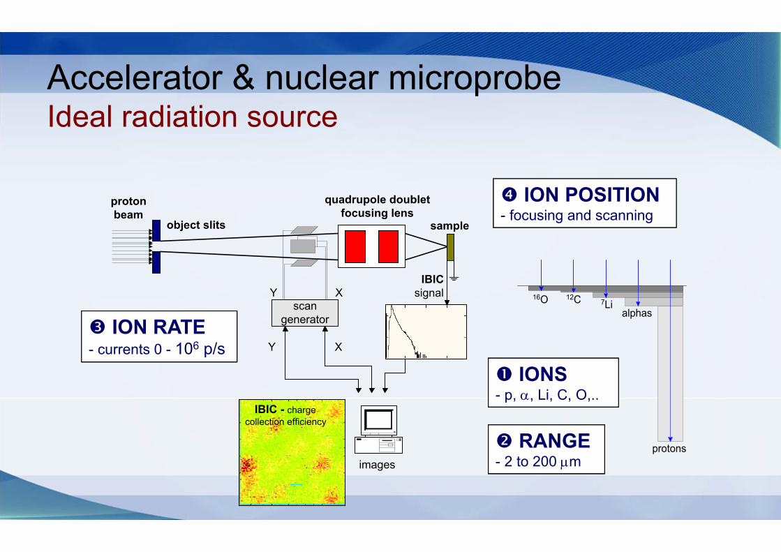
Accelerator & nuclear microprobeAvailable ion beams
Silicon I 127‐ Si 28 C 12 He 4 H 1
Range(µm)E=1 MeV
0.37 1.13 1.6 3.5 16.3
Range (µm)E=10 MeV
3.7 4.8 9.5 69.7 709
AT RBI ‐ terminal voltages – 0.1 to 6 MVIon sources – sputtering, RF alphatross, duoplasmatron
Good selection of ion ranges / dE/dx !!

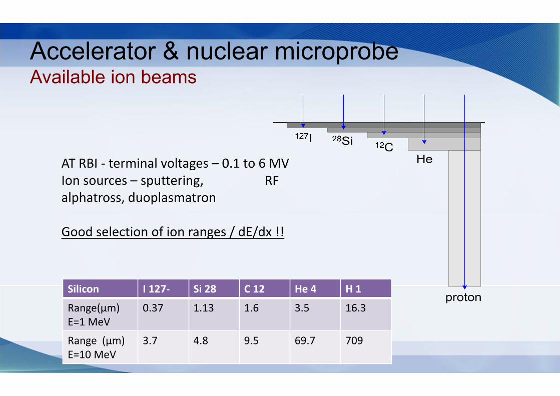
Single ion characterisation:STIM – Scanning Transmission Ion Microscopy:imaging of areal densities (dE/dx)

STIM – Scanning ion transmission microscopy

STIM – Scanning ion transmission microscopy

STIM – Scanning ion transmission microscopy
10 µm
STIM image of copper grid using 8 MeV O3+ ions
STIM – Scanning ion transmission microscopy
Density map for flies wing: 6 MeV O ions (left) and 2 MeV protons (right)
Track shape characterisation

STIM – Scanning ion transmission microscopy
11 MeV 12C3+ ions
high energy lossd ~ 1.68 m
low energy lossd ~ 1.45 m
Combination of STIM with 3D analysisusing C ion induced coincidencespectroscopyO distribution and concentration in z direction ‐ small sample dimensions
~ 15 mm
Bi2Sr2CaCu2O8+ whiskers
17.7 mx
y
z
on axis STIM 28×28 m2

Channeling STIMSTIM (transmission) channeling • currents ≈ 1 fA radiation
damage can be neglected• but, only transmission samples
channeled ions
nonchanneled ions
E0
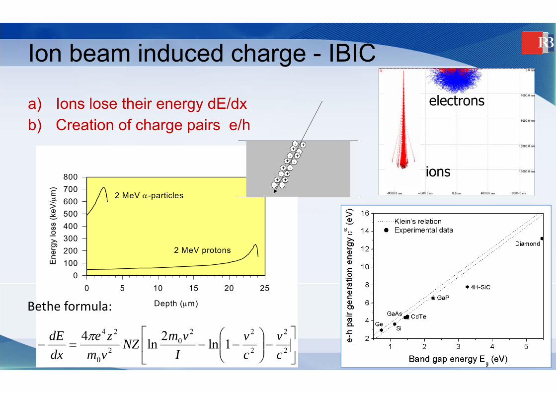
Ion beam induced charge - IBIC
a) Ions lose their energy dE/dxb) Creation of charge pairs e/h
Depth (m)
0 5 10 15 20 25
Ener
gy lo
ss (k
eV/
m)
0100200300400500600700800
2 MeV -particles
2 MeV protons
2
2
2
220
20
24
1ln2ln4cv
cv
IvmNZ
vmze
dxdE
Bethe formula:
ions
electrons
+-
--
-
--
-
-
+ +
++
+
++

Ion beam induced charge - IBIC1. for E 0 charge drift
+-
--
-
--
-
-
+ +
++
+
++
h
he
ed
xhd
xe e
Lde
Ld
QQ 110
h
he
ed
xhd
xe e
Lde
Ld
QQ 110
di = ()iEdi = ()iE
- Charge carriers produced alongthe ion path drift in electric field
- Charge pulse height depends on the local value of electric field, mobility and lifetime of charge carriers.- Collection length
- for constant E, Induced charge signal corresponds to the value of
2. for E = 0 charge diffuse
dxxxr
x dxdEdxx
dxdEY e xL
di
d
d
)(0
dxxxr
x dxdEdxx
dxdEY e xL
di
d
d
)(0
diffusion region
drift region
+
‐
a) Ions lose their energy dE/dxb) Creation of charge pairs e/hc) Charge transport:
1. Drift - in electric field 2. Diffusion
d) Induced chargee) IBIC signal

Ion beam induced charge - IBIC
a) Ions lose their energy dE/dxb) Creation of charge pairs e/hc) Charge transport:
1. Drift - in electric field 2. Diffusion
d) Induced chargee) IBIC signal
V
Q
V
Vout
d
T= 0
-2 0 2 4 6 8 10 12 14
0.000
0.025
0.050
0.075
0.0
0.2
0.4
0.6
0.8
1.0
I
Time
Q
Induced current
Induced charge
v
dvq)t(I
T
0
dt)t(I)t(Q

Ion beam induced charge - IBIC
a) Ions lose their energy dE/dxb) Creation of charge pairs e/hc) Charge transport:
1. Drift - in electric field 2. Diffusion
d) Induced chargee) IBIC signal
V
Q
V
Vout
d
T=10
Induced current
Induced charge
v
dvq)t(I
T
0
dt)t(I)t(Q
-2 0 2 4 6 8 10 12 14
0.000
0.025
0.050
0.075
0.0
0.2
0.4
0.6
0.8
1.0
I
Time
Q

Ion beam induced charge - IBIC
-2 0 2 4 6 8 10 12 14 16
0.000
0.025
0.050
0.075
0.0
0.2
0.4
0.6
0.8
1.0
I
Time
QT
0
dt)t(I)t(Q
-2 0 2 4 6 8 10 12 14
0.000
0.025
0.050
0.075
0.0
0.2
0.4
0.6
0.8
1.0
I
Time
Q
t
dvqtI exp)(
In reality (charge carrier lifetime) can be short due to defects !
Velocity; v dTRMobility; d2/(TR *VBias)

Ion Beam Induced ChargePulse processing (visit ORTEC tutorial)
Charge sensitive preamplification‐ For high resolution PHA
(pulse height analysis)‐ Due to integration, time
structure of the signal is forgotten
‐ Shaping time constant
Current preamplifier‐ For studying of pulse time structure – TRIBIC)
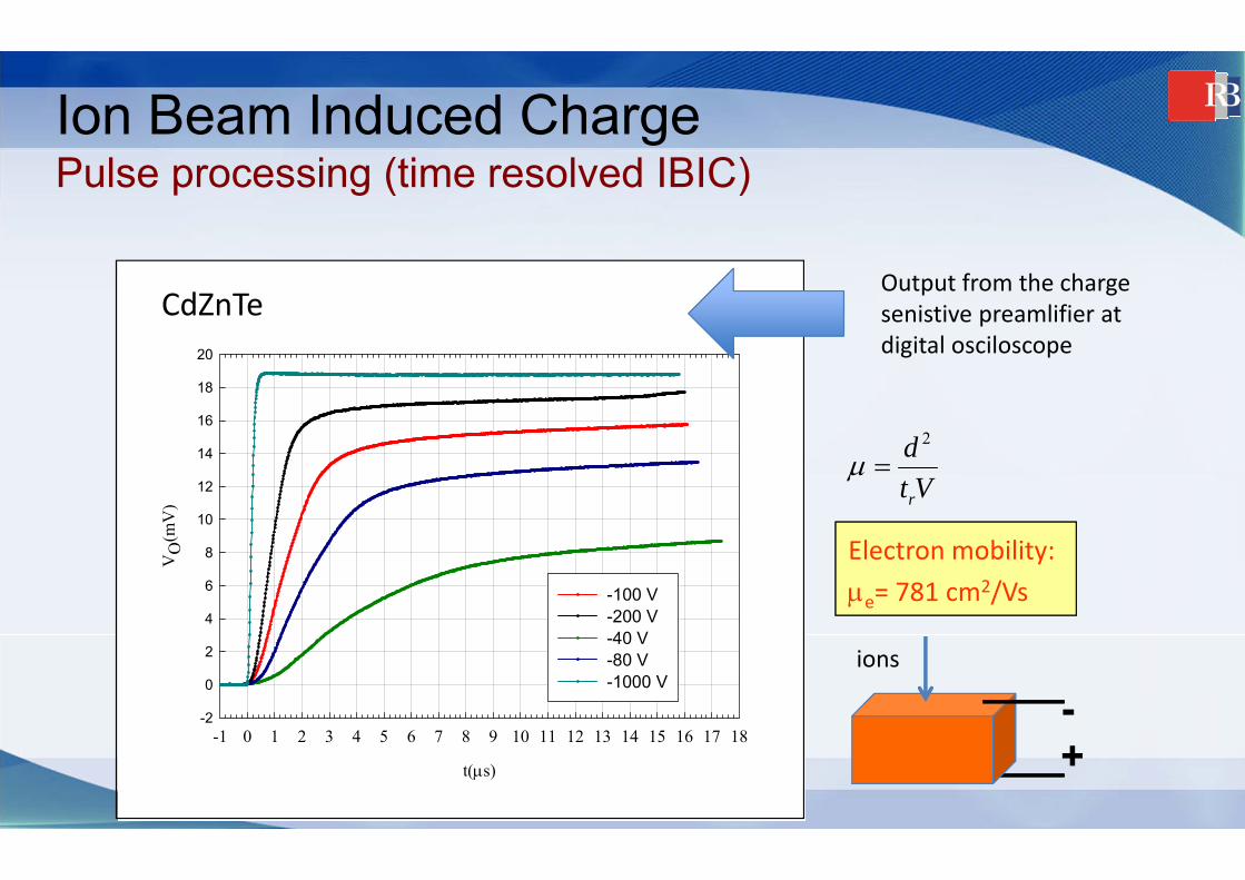
t(s)
-1 0 1 2 3 4 5 6 7 8 9 10 11 12 13 14 15 16 17 18
VO(mV)
-2
0
2
4
6
8
10
12
14
16
18
20
-100 V-200 V-40 V-80 V-1000 V
Electron mobility: e= 781 cm2/Vs
Vtd
r
2
CdZnTeOutput from the charge senistive preamlifier at digital osciloscope
ions
-+
Ion Beam Induced ChargePulse processing (time resolved IBIC)
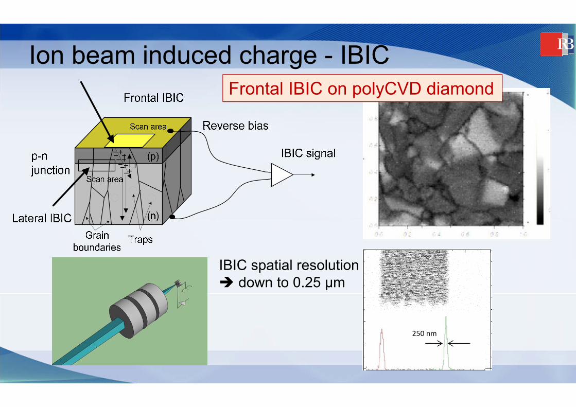
Ion beam induced charge - IBIC
250 nm
IBIC spatial resolution down to 0.25 μm
Frontal IBIC on polyCVD diamond

EFG siliconSchotky diode
Frontal IBIC images can identify distribution of electrically active defects !
Ion beam induced chargeFrontal IBIC

Ion beam induced chargeFrontal IBIC
By proper selection of ion type and energy, CCE (charge collection efficiency) at different sample depths can be imaged.
4.5 MeV Lirange 6μm
3 MeV protonsrange 90 μm
Si Schotky diode
surface
bulk

Ion beam induced charge - IBICLateral IBIC on Si power diode
E = 0
contact and/orheavily dopedregion
pn junction
E < 0
ion beam
0 zd z
(z<zd) = 1
(z>zd) = exp(‐(z‐zd)/Lp,n)hole or electrondiffusion length
50 100 150 200 2500,08
0,10,1
0,2
0,4
0,6
0,811
Lp = ( 27.3 ± 0.8 ) m = (0.57 ± 0.03)s 117.5 V
90.6 V
60.4 V28 V
Col
lect
ion
effic
ienc
y
Depth (m)
CdZnTe
U=+50V ST=2.0s U=+100V ST=2.0s U=+150V ST=2.0s U=+250V ST=2.0s
U=+50V ST=8.0s U=+100V ST=8.0s U=+150V ST=8.0s U=+250V ST=8.0s
In-Au ST=8s
depth (m)0 250 500 750 1000 1250 1500 1750 2000
effic
ienc
y (%
)
0,0
0,1
0,2
0,3
0,4
0,5
0,6
0,7
0,8
0,9
1,0
+50V+100V+150V+200V+250V
electrons
holes
electronsholes
ion beam
CCE 100%
fully depleted device(ideal case)
Ion beam induced charge - IBIC
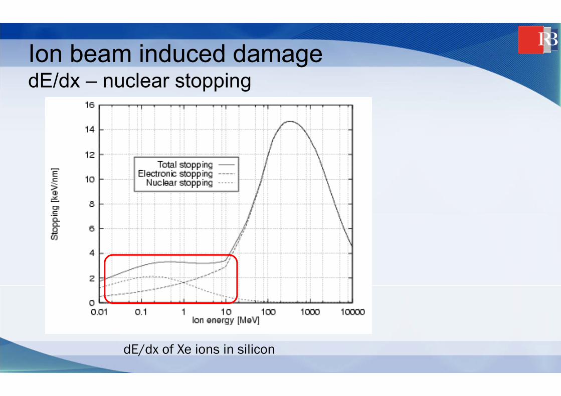
Ion beam induced damagedE/dx – nuclear stopping
dE/dx of Xe ions in silicon

50 Li7 m‐2 = 5 109 cm‐2
6 Li7m‐2 = 6 108 cm‐2
(4 events per pixel)
• For 100% ion impact detection efficiency, IBIC can be used to monitor irradiation fluence
• Irradiation of arbitrary shapes • On‐line monitoring of CCE degradation
Ion microprobe irradiation & IBIC probing

Ion microprobe irradiation & IBIC probing
• By excessive irradiation of small detector regions (e.g. 50 x 50 μm2) induced defects (charge carrier traps) degrade charge collection efficiency (CCE)
• Irradiation fluence and CCE are continuously monitored on-line
• Damaging/probing concept can be used for radiation hardness tests (e.g Si vs. diamond)
V. Grilj et al (RBI, JAEA)Nucl. Instr. Meth. B306 (2013) 191

Ion beam induced charge - IBIC
1E11 1E12 1E13 1E140.5
0.6
0.7
0.8
0.9
1.0
scCVD (150V) membrane (80V) membrane (15V)
CC
E
d [MeV/g]
scCVD diamond membrane detector
CVD diamond membrane provides a trigger for each single ion transmitted to the air
Extreme radiation hardness– equivalent of 1016 cm-2 of 1 MeV neutrons !!
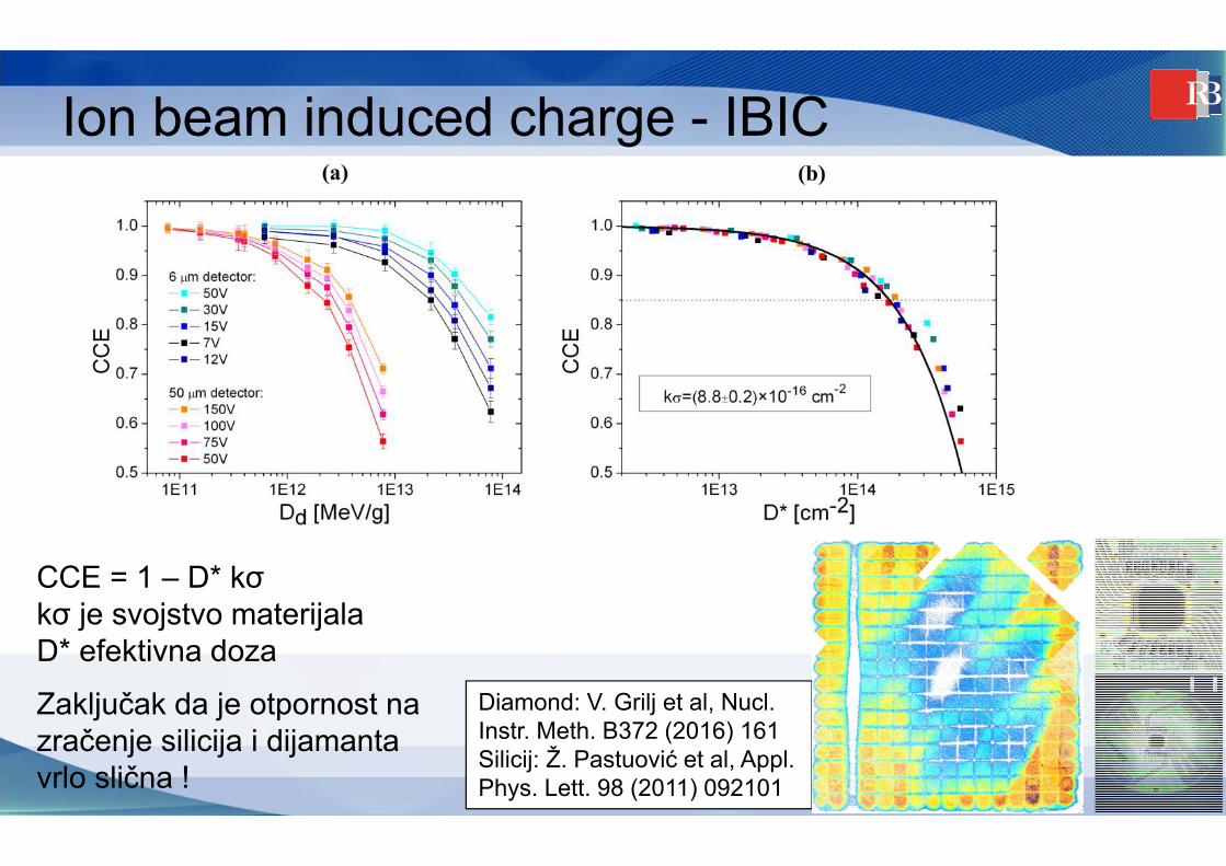
Ion beam induced charge - IBIC
CCE = 1 – D* kσ kσ je svojstvo materijala D* efektivna doza
Zaključak da je otpornost na zračenje silicija i dijamanta vrlo slična !
Diamond: V. Grilj et al, Nucl. Instr. Meth. B372 (2016) 161Silicij: Ž. Pastuović et al, Appl. Phys. Lett. 98 (2011) 092101

Samples: • Si PIN diode Hammamatsu S1223• 4H-SiC Schottky diode
Probing the defect creation process (Si and SiC) Pulsed beam
Irradiation and IBIC probing:• 3.25 MeV C ions (both irradiation
and IBIC probing • Ion range 3.5 μm in Si ( as for 1
MeV He ions )• ton = 1 ms; toff = 0.1 to 50 ms• fluence:
346 μm-2 (Si) 33 μm-2 (SiC)
• 400 pulses
System is typicaly used for MeV SIMS & single ion implantation, irradiation and probing is controlled by SPECTOR

Probing the defect creation process (Si and SiC) Pulsed beam
Irradiation and IBIC probing:• 3.25 MeV C ions (both irradiation
and IBIC probing • Ion range 3.5 μm in Si ( as for 1
MeV He ions )• ton = 1 ms; toff = 0.1 to 50 ms• fluence:
346 μm-2 (Si) 33 μm-2 (SiC)
• 400 pulses
Si pin
4H SiC
Average distance between ions within a single pulse was > 1 μm .... too large for ‘dynamic annealing’ of defects
No statisticaly significant changes have been observed for different ton/toff cycles (millisecond range)

In air IBIC experiment • Large detector structures (e.g. high energy physics
detectors) can not be tested in small vacuum chamber
• Alternative – in air microbeam !• But - beam spot degradation
Degradation of beam spot (in micrometers) for SiN and diamond exit foil
• SOLUTION:• SiN exit foil• up to 2 mm working distance• Proton energy > 6 MeV !!
Energy / air path 100 nm Si3N4 6 µm diamond
3 MeV / 0.5 mm 1.02 9.0
3 MeV / 2.0 mm 4.39 30.6
6 MeV / 0.5 mm 0.50 4.3
6 MeV / 2.0 mm 2.06 14.8
9 MeV / 0.5mm 0.34 2.9
9 MeV / 2.0 mm 1.40 9.9
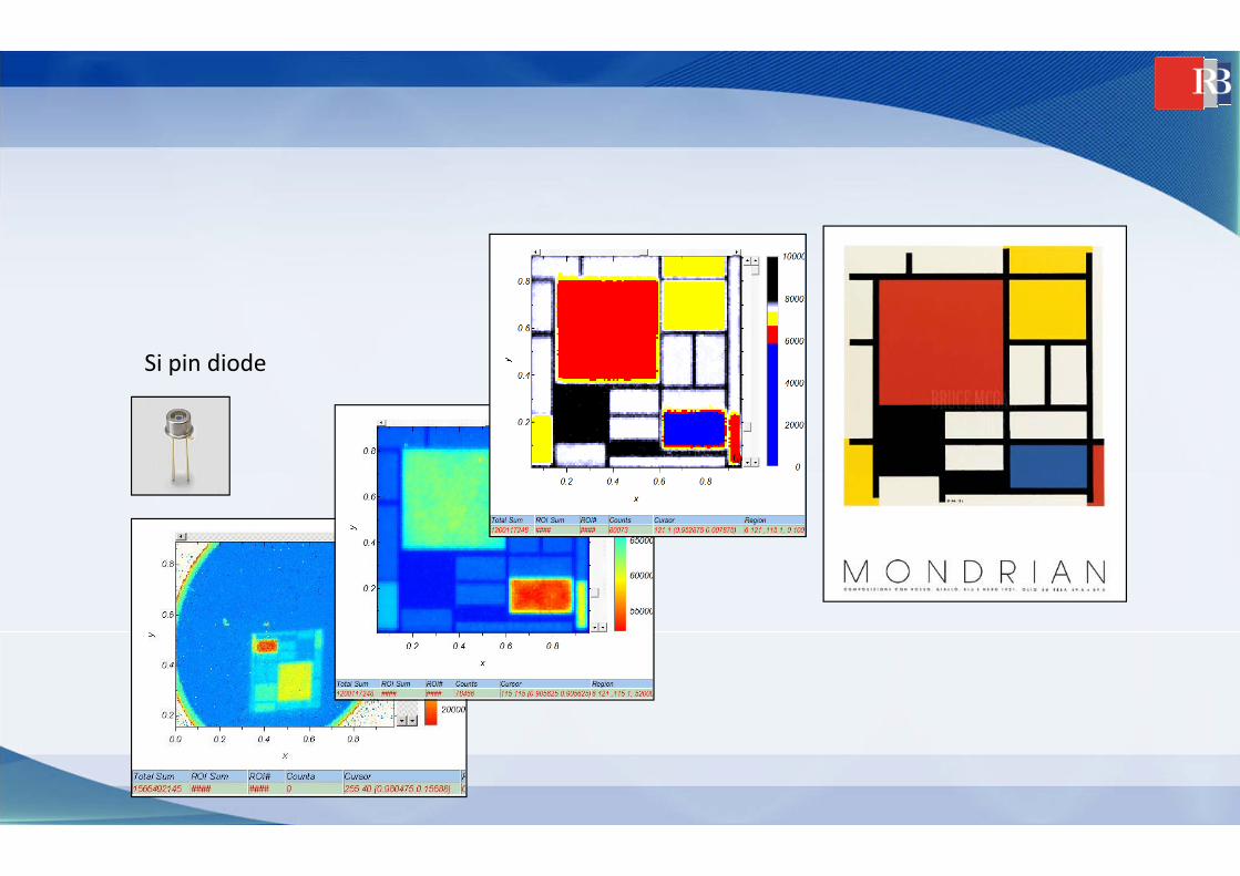
Si pin diode

![Magnetic anisotropy in surface-supported single-ion ...users.physik.fu-berlin.de/~kuch/Bernien_Dy.pdf · Lanthanide single-ion complexes [8,15–18] are promising molecules to overcome](https://static.fdocuments.in/doc/165x107/60196388a19dd2567b578713/magnetic-anisotropy-in-surface-supported-single-ion-users-kuchberniendypdf.jpg)