
Single-Electron Devices and Their Applicationschem.ch.huji.ac.il/~porath/NST2/Lecture 7/Likharev...
62
Full0599.doc Published in Proc. IEEE, vol. 87, pp. 606-632, April 1999 Single-Electron Devices and Their Applications Konstantin K. Likharev Department of Physics, State University of New York at Stony Brook Stony Brook, NY 11794-3800 [email protected] Abstract The goal of this paper is to review in brief the basic physics of single-electron devices, as well as their current and prospective applications. These devices, based on the controllable transfer of single electrons between small conducting "islands", have already enabled several important scientific experiments. Several other applications of analog single-electron devices in unique scientific instrumentation and metrology seem quite feasible. On the other hand, the prospect of silicon transistors being replaced by single-electron devices in integrated digital circuits faces tough challenges and remains uncertain. Nevertheless, even if this replacement does not happen, single-electronics will continue to play an important role by shedding light on the fundamental size limitations of new electronic devices. Moreover, recent research in this field has generated some exciting by-product ideas which may revolutionize random-access-memory and digital-data-storage technologies. Keywords - Single-electron tunneling, Fowler-Nordheim tunneling, single-electron devices, Coulomb blockade, supersensitive electrometry, single-electron spectroscopy, dc current standards, temperature standards, random access memories, floating-gate memories, logic circuits, data storage. I. INTRODUCTION: BASIC PHYSICS AND SCALING The manipulation of single electrons was demonstrated in the seminal experiments by Millikan at the very beginning of the century, but in solid state circuits it was not implemented until the late 1980s, despite some important earlier background work [1-5]. The main reason for this delay is that the manipulation requires the reproducible fabrication of very small conducting particles, and their accurate positioning against external electrodes. The necessary nanofabrication techniques have become available during the past two decades, and have made possible a new field of solid state physics, single-electronics (see Refs. 6-8 for its general reviews). Figure 1 illustrates the basic concept of single-electronics. Let a small conductor (traditionally called an island) be initially electroneutral, i.e. have exactly as many (m) electrons as it has protons in its crystal lattice. In this state the island does not generate any appreciable electric field beyond its borders, and a weak external force F may bring in an additional electron from outside. (In most single-electron devices, this injection is carried out by tunneling through an energy barrier created by a thin insulating layer). Now the net charge Q of the island is (-e), and the resulting electric field E repulses the following electrons which might be added. Though the fundamental charge e ≈ 1.6×10 -19 Coulomb is very small on the human scale of things, the field E is inversely proportional to the square of the island size, and may become rather strong for nanoscale
Transcript of Single-Electron Devices and Their Applicationschem.ch.huji.ac.il/~porath/NST2/Lecture 7/Likharev...

Full0599.doc
Published in Proc. IEEE, vol. 87, pp. 606-632, April 1999
Single-Electron Devices and Their Applications
Konstantin K. LikharevDepartment of Physics, State University of New York at Stony Brook
Stony Brook, NY [email protected]
Abstract
The goal of this paper is to review in brief the basic physics of single-electron devices, aswell as their current and prospective applications. These devices, based on the controllabletransfer of single electrons between small conducting "islands", have already enabled severalimportant scientific experiments. Several other applications of analog single-electron devices inunique scientific instrumentation and metrology seem quite feasible. On the other hand, theprospect of silicon transistors being replaced by single-electron devices in integrated digitalcircuits faces tough challenges and remains uncertain. Nevertheless, even if this replacementdoes not happen, single-electronics will continue to play an important role by shedding light onthe fundamental size limitations of new electronic devices. Moreover, recent research in this fieldhas generated some exciting by-product ideas which may revolutionize random-access-memoryand digital-data-storage technologies.
Keywords - Single-electron tunneling, Fowler-Nordheim tunneling, single-electrondevices, Coulomb blockade, supersensitive electrometry, single-electron spectroscopy, dc currentstandards, temperature standards, random access memories, floating-gate memories, logiccircuits, data storage.
I. INTRODUCTION: BASIC PHYSICS AND SCALING
The manipulation of single electrons was demonstrated in the seminal experiments byMillikan at the very beginning of the century, but in solid state circuits it was not implemented untilthe late 1980s, despite some important earlier background work [1-5]. The main reason for thisdelay is that the manipulation requires the reproducible fabrication of very small conductingparticles, and their accurate positioning against external electrodes. The necessary nanofabricationtechniques have become available during the past two decades, and have made possible a new fieldof solid state physics, single-electronics (see Refs. 6-8 for its general reviews).
Figure 1 illustrates the basic concept of single-electronics. Let a small conductor(traditionally called an island) be initially electroneutral, i.e. have exactly as many (m) electrons asit has protons in its crystal lattice. In this state the island does not generate any appreciable electricfield beyond its borders, and a weak external force F may bring in an additional electron fromoutside. (In most single-electron devices, this injection is carried out by tunneling through an energybarrier created by a thin insulating layer). Now the net charge Q of the island is (-e), and theresulting electric field EE repulses the following electrons which might be added. Though thefundamental charge e ≈ 1.6×10⁻¹⁹ Coulomb is very small on the human scale of things, the field EE isinversely proportional to the square of the island size, and may become rather strong for nanoscale

D:\Likharev\Nano\Reviews\ProcIEEE\Full0599.doc 2
structures. For example, the field is as large as ~140 kV/cm on the surface of a 10-nm sphere invacuum.
The theory of single-electron phenomena (see the next section) shows that a more adequatemeasure of the strength of these effects is not the electric field, but the charging energy
Ec = e2/C, (1)
where C is the capacitance of the island1. When the island size becomes comparable with the deBroglie wavelength of the electrons inside the island, their energy quantization becomes substantial(see, e.g., reviews [10-13]). In this case the energy scale of the charging effects is given by a moregeneral notion, the electron addition energy Ea. In most cases of interest, Ea may be wellapproximated by the following simple formula:
Ea = Ec+ Ek. (2)
Here Ek is the quantum kinetic energy of the added electron; for a degenerate electron gas Ek =1/g(εF)V, where V is the island volume and g(εF) is the density of states on the Fermi surface.
Figure 2 shows the total electron addition energy as a function of the island diameter, ascalculated using Eq. (2) for a simple but representative model. For 100-nm-scale devices whichwere typical for the initial stages of experimental single-electronics, Ea is dominated by thecharging energy Ec and is of the order of 1 meV, i.e. ~ 10 K in temperature units. Since thermalfluctuations suppress most single-electron effects unless
Ea ≥ 10 kBT, (3)
these experiments have to be carried out in the sub-1-K range (typically, using helium dilutionrefrigerators).
On the other hand, if the island size is reduced below ~10 nm, Ea approaches 100 meV,and some single-electron effects become visible at room temperature. However, most suggesteddigital single-electron devices require even higher values of Ea (~ 100 kBT) in order to avoidthermally-induced random tunneling events, so that for room temperature operation the electronaddition energy Ea has to be as large as a few electron-volts, and the minimum feature size ofsingle-electron devices has to be smaller than ~1 nm (Fig. 2). In this size range the electronquantization energy Ek becomes comparable with or larger than the charging energy Ec for mostmaterials; this is why islands this small are frequently called quantum dots. Their use involves notonly extremely difficult nanofabrication technology (especially challenging for large scaleintegration), but also some major physics problems including the high sensitivity of transportproperties to small variations of the quantum dot size and shape. This is why it is very important todevelop single-electron devices capable of operating with the lowest possible ratio Ea/kBT . As wewill see below, some devices may work in the size range where Ec > Ek even at room temperature,thus avoiding complications stemming from the energy quantization effects.
1 For a two-electrode capacitor, the elementary charging energy is of course e2/2C = Ec /2, rather than Ec.However, if a single small conductor is charged with electrons from a source kept at a fixed electrochemicalpotential µ, this is Ec which gives the electrostatic contribution to the energy necessary for the transfer of oneadditional electron to the conductor: e∆µ ≡ Ea ≈ Ec + kinetic energy - see Eq. (2).
D:\Likharev\Nano\Reviews\ProcIEEE\Full0599.doc 3
The objective of this paper is to give a brief review of the present status of applied single-electronics. I will start with an introduction of the theory of single-electron tunneling (Sec. II). Itwill allow us to discuss (in Sec. III) the most important single-electron phenomena, devices andcircuit components. Analog applications of the devices will be described in Sec. IV, while theprospects of digital applications will be discussed in Sec. V. In the concluding Sec. VI, I will try tosummarize my vision of the prospects and problems faced by the field.
Due to the paper length restrictions I will not be able to mention many importantcontributions to the rapidly growing pool of literature on single-electronics; I am expressing myapology to the authors and hope for their understanding.
II. THEORETICAL BACKGROUND
A. Orthodox Theory
Throughout the history of single-electronics, a unique guiding role has been played by asimple but very effective "orthodox" theory which was pioneered (for a particular case) by Kulikand Shekhter [5] and later generalized to other systems - see, e.g., Ref. 7 or Ref. 13 for a detailedreview. The theory makes the following major assumptions:
• The electron energy quantization inside the conductors is ignored, i.e. the electron energyspectrum is treated as continuous. Strictly speaking this assumption is valid only if Ek << kBT, but itfrequently gives an adequate description of observations as soon as Ek << Ec (cf. Fig. 2).
• The time τt of electron tunneling through the barrier is assumed to be negligibly small incomparison with other time scales (including the interval between neighboring tunneling events).This assumption is valid for tunnel barriers used in single-electron devices of practical interest,where τt ~ 10-15 s.
• Coherent quantum processes consisting of several simultaneous tunneling events("cotunneling") are ignored. This assumption is valid if the resistance R of all the tunnel barriers ofthe system is much higher than the quantum unit of resistance RQ :
R >> RQ, RQ = h/4e2 ≈ 6.5 kΩ. (4)
The latter relation is of principal importance for single-electronics as a whole.2
Despite the limitations listed above, the orthodox theory is in quantitative agreement withvirtually all the experimental data for systems with metallic conductors (with their small values ofthe electron wavelength on the Fermi surface, λF) and gives at least a qualitative description ofmost results for most semiconductor structures (where the quantization effects are more noticeable,due to larger λF).
2 This field really took off when it was recognized [14, 15] that Eq. (4) ensures the localization of eachelectron within a particular conducting island of the system at any particular instant. This fact shows thattunnel barriers with low transparency may effectively suppress the quantum-mechanical uncertainty of theelectron location. Notice that only this suppression makes controllable single-electron manipulationpossible. (In this sense single-electronics does not fall into the much advertised category of "quantumelectronic devices". Of course, single-electron devices do use quantum properties of matter, but so dosemiconductor transistors.)

D:\Likharev\Nano\Reviews\ProcIEEE\Full0599.doc 4
The main result of the theory can be formulated as follows: the tunneling of a singleelectron through a particular tunnel barrier is always a random event, with a certain rate Γ (i.e.probability per unit time) which depends solely on the reduction ∆W of the free (electrostatic)energy of the system as a result of this tunneling event. Within the orthodox theory this dependencemay be expressed with a universal formula
Γ(∆W) = (1/e) I(∆W/e) [1 - exp-∆W/kBT]-1, (5)
where I(V) is the "seed" dc I-V curve of the tunnel barrier in the absence of single-electron chargingeffects. (In many cases, the Ohmic approximation I(V) = V/R is quite acceptable.) ∆W may bereadily found from the system's electrostatics; a few simple examples will be considered below.Frequently the following general expressions are rather useful:
∆W = e(Vi + Vf)/2, (6a)or
∆W = e(Vi - Vt),Vt ≡ e(C-1)kl - e[(C-1)kk +(C-1)ll]/2, (6b)
where Vi and Vf are voltage drops across the barrier before and after the tunneling event,respectively, while C-1 is the reciprocal capacitance matrix of the system, and k and l are thenumbers of the islands separated by this particular barrier.
Figure 3a shows the dependence given by Eq. (5); at low temperatures (kBT << ∆W) onlytunneling events decreasing the electrostatic energy (and dissipating the difference) are possible,and their rate is proportional to ∆W. The latter fact is easy to comprehend: an increase in appliedvoltage increases the number of electron states in the source electrode which may provide anelectron capable of tunneling into an empty state of the drain electrode.
Though Eqs. (5) and (6) are rather simple, the calculation of properties of even some basicsingle-electron systems runs into a technical problem: in many situations, several tunneling eventsare possible at the same time, and the orthodox theory only gives the chances of a particularoutcome. Hence, some sort of statistical calculation scheme becomes inevitable. For systems withrelatively few islands, i.e. with a limited set of possible charge states i, Eq. (5) may be pluggedinto the system of "master" equations [5, 14, 15]:
dpi/dt = ∑∑j (Γj→i pj - Γi→j pi ) (7)
describing the time evolution of probability pi of each state. After this system has been solved, theprobabilities pi may be used for a straightforward calculation of average values and fluctuations ofany variable. A nice example of the implementation of this approach is the series of computerprograms SETTRANS for the fast calculation of dc I-V curves and white noise of single-electrontransistors, created by A. Korotkov.3
For more complex systems the multi-dimensional space of all possible charge states maybecome too large, and the only practical method is to simulate the random dynamics of the systemby a Monte Carlo method [16]. In this procedure, Eq. (5) is used to establish the correct statistics ofthe randomly generated events. After a sufficient number of implementations have been
3 MS-DOS versions of these programs are available via anonymous ftp from the sitehana.physics.sunysb.edu/pub/settrans/dos.

D:\Likharev\Nano\Reviews\ProcIEEE\Full0599.doc 5
accumulated, variables of interest may be evaluated by averaging over this ensemble. Severalprograms of this type have been developed by various research groups. Of those publicly available,SIMON developed by C. Wasshuber and his collaborators at the Technical University of Vienna,Austria [17] features a graphical user interface and also allows an approximate account ofcotunneling.4 On the other hand, MOSES developed by R. Chen and collaborators at Stony Brook5
only has a text interface and is limited to the orthodox theory, but allows a broader range of circuitelements and analyses. The currently available version 1.1 of MOSES is also considerably fasterthan the available version 1.3 of SIMON [18]. In certain cases, a combination of both numericalmethods may be useful [19].
B. Effects Beyond the Orthodox Theory
Experiments with single-electron devices have indicated several features which are notaccounted for by the orthodox theory. In non-superconducting systems, the most important effectsare:
1). Cotunneling. This effect was first predicted in 1989 [20] and observed experimentallysoon after [21] (for a review, see Ref. 50). The essence of the effect is that the tunneling of several(N>1) electrons through different barriers at the same time is possible as a single coherentquantum-mechanical process. The rate of this process is crudely (RQ/R)N-1 times less than that forthe single-electron tunneling described by Eq. (5) of the orthodox theory. If the condition expressedby Eq. (4) is satisfied, this ratio is rather small; cotunneling can nevertheless be clearly observedwithin the Coulomb blockade range where orthodox tunneling is suppressed - see Sec. III below.
2). Discrete Energy Levels. For very small islands, the quantum splitting Ek betweenelectron energy levels may become larger than Ec and kBT (see Fig. 2 and its discussion in Sec. I).The generalization of the orthodox theory to this case has been carried out by Averin and Korotkov[23] who considered a situation where tunneling is only possible between islands with discretelevels and larger electrodes where electrons still have a continuous spectrum. They have shown thatif the tunneling barriers are not extremely thin, i.e. their seed tunneling rate Γ0 is not too large (hΓ0
< kBT), the situation may again be described with master equations similar to Eq. (7) of theorthodox theory, but with a different energy dependence of the tunneling rate to/from a certainquantum level:
Γ (∆W) = Γ0 [1 + exp-∆W/kBT]-1. (8)
This dependence (Fig. 4a) repeats (and results from) the Fermi distribution of electrons in the bulkelectrode. (In fact, the orthodox rate (5) may be obtained as a sum of the rates (8) over all the levelsof a continuous spectrum of the island). Another difference is that the summation in the masterequations should be extended over two indices: one for the total number of electrons (as in Eq.(7)), and another for the electron distribution between the energy levels, at a fixed number ofelectrons. This makes the solution to master equations more complex.
4 Information on the distribution of SIMON can be found on the Web sitehttp://members.magnet.at/catsmeow/.
5 MOSES 1.1 is available in both MS-DOS and UNIX versions via anonymous ftp from the sitehana.physics.sunysb.edu/pub/moses.
D:\Likharev\Nano\Reviews\ProcIEEE\Full0599.doc 6
If the system has more than one quantum dot, tunneling between them may becomeimportant. If the energy loss effects are not too significant, this tunneling leads only to coherenthybridization of the quantum dot levels, similar to that well studied in atomic and molecularphysics. Inelastic tunneling from an island to bulk electrodes, described by Eq. (8), may bring asubstantial dissipation into this system and suppress the system coherence - see, e.g., experiments[24-26] with "artificial molecules", and review [12].
In general, energy quantization effects have not yet led to suggestions for any new practicalapplications, with the exception of single-electron spectroscopy (Sec. IV.B) which is still limited tofundamental physics studies, and some highly controversial logic device proposals (Sec. V.B). Thisis why a review of single-electron devices can be based mostly on the predictions of the orthodoxtheory.
III. BASIC SINGLE-ELECTRON DEVICES
Let us start with a discussion of cases in which single-electron charging effects do notappear. First, consider a tunnel junction with a fixed voltage V across it (Vi = Vf = V). Here, for twopossible directions of electron tunneling, Eq. (6) yields ∆W = ± eV, and according to Eq. (5) the netcurrent is I = e × [Γ(eV) - Γ(-eV)] = I(V), i.e. we have come back to the seed dc I-V curve. This isnatural, since in this system a single-electron tunneling event does not change V, i.e. the single-electron charge quantization does not lead to any noticeable effects,6 even if the junction size is verysmall. A possible way to describe the same fact is to say that the large stray capacitance of theexternal electrodes leading to the junction adds up to the junction capacitance (however small), sothat the total capacitance C does not satisfy the condition (3).7
Even more importantly, the orthodox theory predicts that the effects of single-electrondiscreteness may be ignored in any solid state device which does not have small conducting islandsseparated from the external electrodes by sufficiently high tunnel barriers. (The quantitativecriterion of the notion "high barrier" is provided by Eq. (4)). The most important practical examplemay be a small-size MOSFET which does not exhibit any immediate single-electron effects even ifthe average number of carriers in its channel is smaller than one, since in these devices the channel-contact resistance is typically much lower than RQ. The physical interpretation of this fact is that insystems without sufficiently high tunnel barriers the electron wavefunctions are well extended, andelectrons cannot be treated as classical, localized particles.
Now let us turn to situations in which the single-electron charging effects do appear.
A. Single-Electron Box
Figure 5a shows the conceptually simplest device, the "single-electron box".8 The deviceconsists of just one small island separated from a larger electrode ("electron source") by a tunnel
6 Besides shot noise which appears at eV/2 > kBT.
7 More detailed analysis [14, 15] shows that even if the stray capacitance is carefully eliminated, the single-electron charging effects would not show up, because the lead impedance Z(ω) is typically much less than thequantum unit of resistance (4), and as a result, quantum fluctuations of the environment smear out thecharging effects. A quantitative theory of this smearing has been developed by Nazarov [27]. (A simplerderivation of the same result was given by Devoret et al. [28]; see also the review [13].)

D:\Likharev\Nano\Reviews\ProcIEEE\Full0599.doc 7
barrier. An external electric field may be applied to the island using another electrode ("gate")separated from the island by a thicker insulator which does not allow noticeable tunneling. The fieldchanges the electrochemical potential of the island and thus determines the conditions of electrontunneling. Elementary electrostatics shows that the free (Gibbs) energy of the system may bepresented as
W = Q2/2CΣ + (C0/CΣ)QU + const, (9)
where Q = -ne is the island charge (n is the number of uncompensated electrons), C0 is the island-gate capacitance, while CΣ is the total capacitance of the island (including C0). Usually, thisexpression is re-written as
W = (ne - Qe)2/2CΣ + const, (10)
where parameter Qe, which is defined as
Qe ≡ UC0, (11)
is usually called the "external charge". The physical sense of this definition only becomes apparentfor the case when the electric field between the gate and island is well localized (Fig. 5b); then (-Qe) is just the polarization charge of the island which is bound by the gate field and is thus takenout of the energy balance of the tunnel junction.
From the definition (9) it is evident that in contrast with the discrete total charge of theisland, the variable Qe is continuous, and may be a fraction of the elementary charge e. At lowtemperatures Eq. (5) shows that the single-electron tunneling merely minimizes W; an elementarycalculation using Eq. (10) shows that Q is a step-like function of Qe, i.e. of the gate voltage (Fig.5c), with a fixed distance between the neighboring steps:
∆Qe = e, ∆U= e/C0 = const. (12)
If the temperature is increased to kBT ~ Ec, this "Coulomb staircase" is gradually smeared out bythermal fluctuations.
The physics of the Coulomb staircase is very simple: increasing gate voltage U attractsmore and more electrons to the island. The discreteness of electron transfer through low-transparency barriers necessarily makes this increase step-like. This is all very natural andapparently trivial. What is surprising is that even such a simple device allows a reliableaddition/subtraction of single electrons to/from an island with an enormous (and unknown) numberof background electrons, of the order of 1 million in typical low-temperature experiments with 100-nm-scale aluminum islands. This is of course simply a consequence of the enormous strength of theunscreened Coulomb interaction, which has already been discussed in Sec. I.
Notice, however, two major drawbacks of the single-electron box as an electronic circuitcomponent. First, it does not have internal memory: the number n of the electrons in the box is aunique function of the applied voltage U, so that this structure cannot be used for information
8 The basic properties of this system were well understood by Lambe and Jaklevic [4] in the context of theirexperiments with granular tunnel structures, while its quantitative theory was given by Kulik and Shekhter[5]. Experimentally, however, the properties of a single device were not measured until 1991 [29].

D:\Likharev\Nano\Reviews\ProcIEEE\Full0599.doc 8
storage. The second problem is that the box cannot carry dc current, so that an ultrasensitiveelectrometer is necessary to measure its charge state - see, e.g., Ref. 29.
B. Single-electron Transistor
The latter drawback may be easily corrected by splitting the tunnel junction of the single-electron box and applying a dc voltage V between the two, now separate, parts of the externalelectrode (Fig. 6a). The resulting "single-electron transistor"9 is probably the most importantdevice in this field. The device is reminiscent of a usual MOSFET, but with two tunnel barriersembedded in a small conducting island, instead of the usual inversion channel.
The expression for the electrostatic energy W of the system
W = (ne - Qe)2/2CΣ - eV[n1C2 + n2C1]/CΣ + const (13)
is an evident generalization of Eq. (5). Here n1 and n2 are the number of electrons passed throughthe tunnel barriers 1 and 2, respectively, so that n = n1 - n2, while the total island capacitance CΣ isnow a sum of C0, C1, C2, and whatever stray capacitance the island may have. The external chargeQe is again defined by Eq. (11) and is just a convenient way to present the effect of the gate voltageU.
Figure 6b shows typical dc I-V curves of this system. At small source-drain voltage V thereis no current, since any tunneling event would lead to an increase of the total energy (∆W <0) andhence according to Eq. (5) at low enough temperatures (kBT <<Ec ) the tunneling rate isexponentially low. (Cotunneling provides in this region a weak current proportional to RQ
2/R1R2 [20,21], where R1,2 are the tunnel barrier resistances; as far as R1,2 >> RQ, this current is small.) Thissuppression of dc current at low voltages is known as the Coulomb blockade.10
At a certain threshold voltage Vt the Coulomb blockade is overcome, and at much highervoltages the dc I-V curve gradually approaches one of the offset linear asymptotes: I → (V +sign(V)×e/2CΣ)/(R1+R2). On its way, the I-V curve exhibits quasi-periodic oscillations of its slope,closely related in nature to the Coulomb staircase in the single-electron box, and expressedespecially strongly in the case of a strong difference between R1 and R2.
The most important property of the single-electron transistor is that the threshold voltage, aswell as the source-drain current in its vicinity, is a periodic function of the gate voltage, with theperiod given by Eq. (12). This periodicity is evident from Eqs. (10) and (13): if U is changed by∆U= e/C0, Qe changes by e, and may be exactly compensated for by one of the electrons tunnelinginto/from the island. The physical reason for this periodic dependence U (the so-called "Coulombblockade oscillations") is clear from Figs. 5b and 6a: the effect of the gate voltage is equivalent tothe injection of charge Qe = C0U into the island and thus changes the balance of the charges attunnel barrier capacitances C1 and C2, which determines the Coulomb blockade threshold Vt. In theorthodox theory, the dependence Vt (U) is piece-linear and periodic (Fig. 6c).
The first successful experimental implementation of the single-electron transistor wascarried out by Fulton and Dolan [31], using a relatively simple technique in which two layers of
9 It was invented in 1985 [15, 30], on the background of the earlier work on double-junction systems withoutthe gate [3, 5] and on a similar Cooper-pair system [14].10 This term was introduced in Ref. 15, but the phenomenon itself had been qualitatively understood muchearlier, initially for different systems - see, e.g., Refs. 1, 2.

D:\Likharev\Nano\Reviews\ProcIEEE\Full0599.doc 9
aluminum are evaporated in-situ from two angles through the same suspended mask formed bydirect e-beam writing. (This technique, pioneered by G. Dolan [32], has become standard for 100-nm-scale metallic single-electron devices.) Since then single-electron transistors have beendemonstrated in numerous experiments using a wide variety of device geometries, materials, andtechniques. Of course some of the methods used may be more suitable for future integrated circuitfabrication than others (right now, none of them is fast or reproducible enough for VLSIapplications). Unfortunately, the paper length restrictions do not allow me to go into any detailedanalysis and critical comparison of these techniques, so I will only mention the most importantrecent trend.
Over the past few years there has been rapid progress in the fabrication of the firsttransistors with 10-nm-scale islands, with electron addition energies above 10 mV - see Refs. 33-45 and Table 1. The most advanced of these devices, with Ea beyond ~100 meV, exhibit noticeableCoulomb blockade oscillations at room temperature.11
Table 1. Some high-Ea single-electron transistors.
Materials(Island; Barrier) Fabrication Method
HighestEa (meV) Ref.
Al; AlOx Evaporation through an e-beam-formed mask 23 [39]CdSe; organics Nanocrystal binding to prepatterned Au electrodes 60 [44]Al; AlOx Evaporation on a Si3N4 membrane with a nm-scale orifice 92 [42]Ti; Si Metal deposition on prepatterned silicon substrates 120 [43]Carboran molecule E-beam patterned, thin-film gate; STM electrode 130 [40]Si; SiO2 E-beam patterning + oxidation of a SIMOX layer 150 [37]Nb, NbOx Anodic oxidation using scanning probe 1,000 [45]
As the transistor island becomes smaller, the effects of energy quantization may becomeimportant. The application of the double-index master equations to the single-electron transistorshows that its dc I-V curves may be quite complex [50]. However, the situation at small source-drain voltage is much simpler. In fact, Fig. 6c shows that on each period of the Coulomb blockadeoscillations there is one special point Qe = e(n + 1/2), at which the Coulomb blockade is completelysuppressed, and the I-V curve has a finite slope at low voltages Fig. 6b). Another way to expressthe same property is to say that the linear conductance G ≡ dI/dVV=0 of the transistor as a functionof the gate U voltage exhibits sharp peaks. Theory shows that even if the electron quantizationeffects are substantial, the peak position may be found from a very natural "resonance tunneling"condition [9, 50, 51]: an energy level inside the island (with the account of the gate field potential)should be aligned with the Fermi levels in source and drain, which coincide at V→0. This ruleyields a simple equation for the gate voltage distance between the neighboring Coulomb blockadepeaks:
∆U = (CΣ /C0) Ea/e. (14)
11 Several high Ea values recorded for bare double-junction systems (without a gate) should also bementioned [46-49].

D:\Likharev\Nano\Reviews\ProcIEEE\Full0599.doc 10
If the charging effects dominate (Ec >> Ek) this relation is reduced to Eq. (12) of the orthodoxtheory, but at strong quantization (Ek >> Ec) the distance between the Coulomb blockade oscillationpeaks, as well as the height Gmax of the peaks, may vary from level to level.
C. Single-electron Trap
A different generalization of the single-electron box (Fig. 5a) may be obtained by replacingthe single tunnel junction with a one-dimensional array of N > 1 islands separated by tunnel barriers(Fig. 7a).12 The main new feature of this system is its internal memory (bi- or multistability): withincertain ranges of applied gate voltage U the system may be in one of two (or more) charged statesof its edge island.
The reason for this multistability is as follows: due to electric polarization effects anelectron located in one of the islands of the array extends its field to a certain distance [16, 55]. Interms of the island numbers, this distance is of the order of
M = (C/C0)1/2, (15)
where C0 is the effective stray capacitance of the island, while C is the mutual capacitance betweenthe neighboring islands (usually dominated by that of the tunnel junction). This "single-electronsoliton" interacts with the array edges (is attracted to them) at a distance of the order of M. As aresult, the electrostatic self-energy of the soliton has a maximum
Wmax ≈ (e2/2C)×min(M, N/4) (16)
somewhere in the middle of the array (see the middle trace in Fig. 7b). By applying sufficientlyhigh gate voltage U = U+ the energy profile may be tilted enough to drive an electron into the edgeisland; if the array is not too long (N ≤ M), other electrons feel its repulsion and do not follow. If thegate voltage is subsequently decreased to the initial level, the electron is trapped in the edge island,behind the energy barrier. In order to remove the electron from the trap, the voltage has to bereduced further, to U- < U+ (the upper trace in Fig. 7b). As a result, the n(U) dependence exhibitsregions of bi- or multi-stability, in which the charge state of the trap depends on its prehistory (Fig.7c).
The lifetime of a certain state within the multi-stability region is fundamentally limited bythe thermal activation over the energy barrier, and cotunneling [20, 56]. The first effect isexponentially low in Ec/kBT (see Eq. (5) and its discussion), while the second effect fallsexponentially with the array length N [48, 51]. As a result, electron retention time may be very long[56].
After several preliminary attempts [52, 57], single-electron traps with retention time of atleast 12 hours (limited only by the observation time) were successfully demonstrated [58] at lowtemperatures. Their quantitative characteristics were found [59] to be close to the theoreticalpredictions, with allowance for the uncertainties of island geometry and randomness of backgroundcharge (see Sec. IV.C below). Later similar experiments were carried out by another group [60].
D. Single-electron Turnstile and Pump
12 To my knowledge, this device was first discussed in 1991 [52, 53], but in fact it may be considered just aparticular operation mode of the single-electron turnstile (see Sec. D below) which was invented earlier [54].

D:\Likharev\Nano\Reviews\ProcIEEE\Full0599.doc 11
Combining both generalizations of the single-electron box, described in Sec. C and D, wenaturally arrive at the device shown in Fig. 8a. This "single-electron turnstile" was suggested anddemonstrated by a French-Dutch collaboration in 1990 [54]. At V = 0, the device operates exactlylike the single-electron trap: one electron may be pulled into the central island (at random, fromeither source or drain) increasing the gate voltage U beyond a certain threshold; then it may bepushed out by decreasing U. The application of a modest drain-source bias V≠0 breaks the source-drain symmetry: now an electron is always picked up from the source when U goes up anddelivered to the drain when U goes back down. If the gate voltage is cycled periodically, oneelectron is transferred from source to drain each period.
The latter function may be performed even better by another device, the "single-electronpump" ([61], Fig. 8b). Here rf waveforms Ui(t) applied to each gate electrode are phase-shiftedforming a potential wave gliding along the island array. This wave picks up an electron from thesource and carries it down to the drain in very much the same way that the charge-coupled devices(see, e.g., Ref. 62) transfer multi-electron bundles. Notice that this device does not need dc source-drain voltage: the direction of the transferred electron is determined by that of the running wave ofelectric potential.
E. SET Oscillators
Much of the initial excitement around single-electron tunneling was induced by theprediction [15] that it could be used to generate narrowband oscillations with a frequencyfundamentally proportional to dc current:
fSET = I/e. (17)
Conceptually, the simplest system capable of proving these "SET" (from "single-electrontunneling") oscillations may be formed from a single-electron box (Fig. 5a) by replacing thecapacitance C0 with an Ohmic resistor Rs that satisfies the following requirement:
Rs>>R>>RQ. (18)
Figure 9a shows the resulting simple device, while Fig. 9b illustrates its dynamics. Theory says thatSET oscillations should arise as soon as applied dc voltage V exceeds the Coulomb blockadethreshold Vt = e/2C and gradually disappear in background shot noise at I ≥ 0.1e/RC. Experimentalimplementation of this device is not, however, easy for the following reason.
The theory of SET oscillations implies that what we call the Ohmic resistor provides acontinuous transfer of charge, i.e. is capable of transferring sub-single-electron amounts ofelectricity in order to recharge the island capacitance in time intervals between the subsequenttunneling events (Fig. 7b). This assumption, though seemingly counterintuitive, is supported by theobservation that the macroscopic diffusive conductors do not exhibit shot noise at voltages V >kBT/e, as should happen at the discrete transfer of electrons (and as really happens, e.g., in tunneljunctions). The theoretical explanation of the continuous conduction in such conductors is based onthe extended character of the electron - see, e.g., Ref. 7. For the implementation of a narrowbandSET oscillator, however, the Ohmic resistor has to combine the continuous transfer of charge withvery high resistance (~1 MΩ or higher) and very small stray capacitance (~C <<e2/kBT).
After a decade-long effort by several groups [63-69], this goal has been only partly met:continuous transport was demonstrated in ultra-thin-film strips with specific resistance up to about

D:\Likharev\Nano\Reviews\ProcIEEE\Full0599.doc 12
10 kΩ/µm, i.e. Rs ~105 Ω for 10-µm-scale length which gives a still acceptable capacitance for sub-1-Kelvin experiments. The resulting range Rs/RQ is too small to satisfy the strong conditions (18);this is why only questionable evidence of SET oscillations in a single-junction system has beenobtained [64]. (The SET oscillations with frequency expressed by Eq. (17) were observed morereliably although indirectly [70] in 1D junction arrays which may provide quasi-sub-electrontransport of charge [16, 71].)
F. Superconductor Systems
In systems with superconducting electrodes the single particle charging effects may bemore complicated. What follows is a list of the major new features:
1). The seed dc I-V curve of a single junction, which participates in Eq. (5), may be verynonlinear even at small (millivolt - scale) voltages, due to superconducting energy gap ∆ in thedensity of states - see, e.g., Chapter 3 of Ref. [72]. In particular, due to this feature, the chargesensitivity of single-electron transistors with superconducting electrodes may be considerably betterthan in the normal state [73].
2). If a superconducting island has an even total number of electrons, at low temperatures(kBT<< ∆) they are all bound into Cooper pairs. This is why the addition of a new, odd electronrequires the energy Ea + ∆, while the addition of the next, even electron, takes Ea - ∆. These "parityeffects" predicted in 1992 [74] and repeatedly observed experimentally (see, e.g., Refs. 75-77) maysubstantially affect the dynamics of single-electron devices.
3). If the normal resistance of a tunnel barrier is relatively low, R ≤ (∆/Ec)RQ, thecombination of charging and Josephson coupling makes tunneling of single Cooper pairs possible.Since Cooper-pair tunneling is always elastic, its properties differ considerably from that of singleelectrons. For example, the superconducting versions of single-electron devices may havequantized energy levels [14]; this level structure has been observed in recent experiments [78, 79]with so-called Bloch transistors, i.e. Cooper-pair analogs of single-electron transistors, see Fig.6a.13 Another important property of the Bloch transistor is that it may exhibit a finite source-drainsupercurrent with amplitude being a 2e-periodic function of Qe. This prediction [80, 81] has beenconfirmed in numerous experiments - see, e.g. Ref. 82. In resistively-coupled superconductordevices (such as that shown in Fig. 9a) the Cooper-pair tunneling may result in the generation ofso-called "Bloch oscillations" [14] with frequency
fB = I/2e. (19)
either instead of or on top of the SET oscillations. These oscillations (which present a dualquantum-mechanical analog of the usual Bloch oscillations in solids, see, e.g., Ref. 83) have beenobserved experimentally [63].
IV. ANALOG APPLICATIONS
A. Supersensitive Electrometry
13 Bloch transistor was first suggested and analyzed in 1986 [80, 81].

D:\Likharev\Nano\Reviews\ProcIEEE\Full0599.doc 13
If the source-drain voltage V applied to a single-electron transistor is slightly above itsCoulomb blockade threshold Vt, source-drain current I of the device is extremely sensitive to thegate voltage U. In fact, Fig. 6b shows that even the changes δU corresponding to sub-single-electron variations δQe of the external charge lead to measurable variations of I. This extremelyhigh sensitivity has been suggested [30] as a basis for supersensitive electrometry. Calculationsbased on the orthodox theory have shown [84] that the sensitivity of such an electrometer is notvery impressive if the internal capacitance Ci of the signal source is large on the scale of e2/kBT (atsub-1-K temperatures, above ~ 0.1 pF). On the other hand, if the source is so small and so close tothe single-electron transistor that Ci of the order of the capacitances of the transistor C1,2, whitenoise limits the charge sensitivity at an extremely low level, (δQe)min/∆f1/2 < 10-5 e/√Hz, for thedevices with routinely achieved 100-nm-scale islands (here ∆f is the measurement bandwidth).
Since the technology of fabrication of tunnel barriers for single-electron devices is still in itsinfancy, they apparently contain many electron trapping centers and other two-level systemscapable of producing "telegraph noise" - random low-frequency variations of the barrierconductance. This may explain the fact that the excess 1/f-type noise resulting from these variationsexceeds [85] the fundamental white noise up to very high frequencies (apparently at least a fewMHz). Only in high-frequency experiments [86] has the white noise been observed (and shown tovary in accordance with the theoretical predictions). This is why the best charge resolution obtainedat relatively low frequencies (~10 Hz) was somewhat lower than 10-4 e/√Hz [87-89]. Nevertheless,even with this "high" noise, these electrometers are some 6 orders of magnitude more sensitive thatthe best commercially available instruments, and about 100 times more sensitive than speciallydesigned low-temperature semiconductor devices (see, e.g., Ref. 90, 91). In a very recent work[92] in which GHz-range modulation was used to get away from a part of the 1/f noise, a chargesensitivity close to 10-5e/√Hz (at ~1 MHz) was demonstrated. This result gives hope thatelectrometers with the white-noise-limited sensitivity (~10-5e/√Hz at helium temperatures and ~10-
4 e/√Hz at room temperatures) will be routinely available in the near future14.
The high sensitivity of single-electron transistors has already enabled several groups to usethem as electrometers in unique physical experiments. For example, they have made possibleunambiguous observations [75-77] of the parity effects in superconductors, mentioned in Sec. II.Gabove. Absolute measurements of extremely low dc currents (~10-20 A) have been demonstrated[94]. The transistors have also been used in the first measurements of single-electron effects insingle-electron boxes [29] and traps [52, 57-60]. A modified version of the transistor has been usedfor the first proof of the existence of fractional-charge excitations in the fractional quantum Halleffect [95]. Another recent example is the sensitive measurement of local variations in the chemicalpotential of 2D electron gas in GaAs/AlGaAs heterostructures [96, 97]. Further application of theseunique electrometers in scientific experimentation is certainly imminent.
Finally, a new exciting field has been opened by the work of a Lucent Technologies group[98] who have managed to fabricate a single-electron transistor on the tip of a scanning probe andwith its help implement a new type of scanning microscopy, combining submicron spatialresolution with sub-single-electron sensitivity. This novel technique has already been used toobserve single charged impurities in GaAs/AlGaAs heterostructures.
14 Another important trend is the integration of single-electron transistors with field-effect transistorsproviding the next amplification stage, and more importantly the matching of the very high output impedanceof the SET to that of usual RF transmission lines. This allows the useful bandwidth of the single-electrontransistor electrometers to be raised to tens MHz - see, e.g., Refs. 89, 93.

D:\Likharev\Nano\Reviews\ProcIEEE\Full0599.doc 14
B. Single-electron spectroscopy
Another useful spin-off of single-electron electrometry is the possibility of measuring theelectron addition energies (and hence the energy level distribution) in quantum dots and othernanoscale objects, pioneered by M. Kastner's group at MIT [99].
There are two natural ways to carry out such measurements. The first is to use the quantumdot as the island of the single-electron box, capacitively coupled to the single-electron transistor orother sensitive electrometer [90, 100]. The second is to use the quantum dot directly as the island ofa weakly biased single-electron transistor (V →0 ), and measure the gate voltages Un providing thesharp increase of the source-drain conductance G - see Eq. (14) and its discussion. The lattermethod is technically simpler (only one small island is needed) and is preferred by most groups.Moreover, the height of the conduction peak gives additional information on the correspondingelectron wavefunction distribution in the dot (see, e.g., Refs. 90, 101).
Single-electron spectroscopy was first applied to laterally-confined "puddles" of 2Delectron gas in semiconductor heterostructures with lateral [102] or vertical [103] tunneling tosource and drain. Recently, this technique was also used to study electron addition spectra ofnanometer metallic particles [42, 104], naturally formed nanocrystals [44, 105], C60 buckyballs[46], and carbon nanotubes [106, 107], with good prospects to have it extended to numerousnanoobjects, first of all organic macromolecules and clusters [40, 47, 49]. Presently single-electronspectroscopy is developing virtually independently of other applications of single-electronics. Thisis why I will make no attempt to review it in any detail; for recent reviews the reader is referred,e.g., to Ref. 12 . I would like, nevertheless, to offer one remark.
Most of the semiconductor quantum dots studied experimentally by single-electronspectroscopy have shown that their energy spectra are irreproducible and only distantly related tothose of the idealized simple objects studied in most theoretical works. This is quite understandabletaking into account the fact that the dots have numerous electron scattering centers and/or shapeirregularities. (These objects are sometimes called "artificial atoms", but so far these atoms arecertainly not as tidy as the natural ones.) In the presence of uncontrollable inhomogeneities, the onlyavailable approach to sort out single-electronics data is statistical. The few past years were markedby rapid experimental and theoretical progress in this direction, especially after it was recognizedthat in some cases the results may be adequately described by the well-developed random matrixtheory - see, e.g., Ref. 108.
This progress should not conceal the fact that there is very little chance of practicalapplication of single-electron devices with random electron addition energies, especially inintegrated circuits (see Sec. V below). In this context the only hope is that better nanofabricationtechniques will give us more reproducible structures in future. The recent unique experiments by S.Tarucha, L. Kouwenhoven and their collaborators [109] gave the first evidence of a semi-quantitative agreement between the experiment and quantum calculations assuming a simple dotgeometry, presumably indicating that reproducible quantum dots may eventually be possible afterall. Unfortunately, even that would hardly solve the related problem of random background charges- see Sec. V.C below.
C. DC Current Standards
Another possible application of single-electron tunneling is fundamental standards of dccurrent. The initial suggestion for such a standard [14, 15] was to phase lock SET oscillations (17)

D:\Likharev\Nano\Reviews\ProcIEEE\Full0599.doc 15
or Bloch oscillations (19) in a simple oscillator (Fig. 9), with an external rf source of a wellcharacterized frequency f. The phase locking would provide the transfer of a certain number m ofelectrons per period of external rf signal and thus generate dc current which is fundamentallyrelated to frequency as I = mef. Later it turned out to be more convenient to use such a stable rfsource to drive devices such as single-electron turnstiles and pumps (see Sec. III.E above), whichdo not exhibit coherent oscillations in the autonomous mode.
Already the first experiments [54] with the 2+2-junction turnstile have shown that itsrelative accuracy δI/I can be as good as ~10-3. The following theoretical work [110-113] hasindicated that even better accuracy may be provided by the pumps, since these devices allow amore gentle transfer of the single-electron along its array, and leave less margin for the parasiticprocesses of thermal activation and cotunneling which may result in error (say, the occasionaltransfer of an extra electron). An additional advantage of the pump is the possibility ofcompensating for the random background charge of each island (see below) with a specially tuneddc voltage bias applied to each gate. Theory indicates [113] that the known effects limit theaccuracy of a 5-junction turnstile with typical present-day parameters and waveforms at the level of~10-12 at f~10 MHz, and even down to 10-16 if special waveforms are used.
The best experimental effort so far gave an accuracy of 1.5×10⁻⁸ [114], presumably limitedby the photo-excitation of extra electrons by some multi-GHz electromagnetic radiation creepinginto the system. Though finding and mending these radiation leaks may present a problem,apparently it can be solved as evidenced by the above-mentioned experiments with single-electrontraps [58, 60]. Thus I have no doubt that a dc current standard with relative accuracy better than 10-
10 (sufficient for all the suggested applications - see, e.g., Ref. 115) can be implemented usingpump-type devices.
A greater challenge is a substantial increase in the output current of single-electronstandards (presently in the pA range) which would allow much broader application of thesedevices in metrology. A direct increase of the drive frequency f in pump-type devices runs into theproblem of rapidly growing dynamic error rate, as soon as it becomes comparable to 1/RC [111-113]. One way to avoid this problem is to use a single-Cooper-pair version of the pump; heretunneling is elastic, and the drive frequency may be much higher, eventually limited only by theenergy gap of the superconducting materials used at a few tens GHz (I = ef ~ few nA).Unfortunately, these devices are still plagued with the occasional quasiparticle "poisoning", thepossible reasons for which are not well understood - see, e.g., Ref. 74.
Another way may be getting rid of the tunneling altogether. In fact, instead of waiting untilan electron tunnels through a barrier separating two islands of a pump, it would be much better tocarry it over, trapped in a potential well moving along a solid state structure, just as is done withmulti-electron bundles in charge-coupled devices [62]. An interesting attempt to implement such astructure using surface-acoustic waves in a GaAs channel is described in Ref. 116. I believe,however, that a more straightforward way would be a direct scaling down of electric-field-controlled silicon-based CCD structures, simultaneously with their cooling to sub-Kelvintemperatures (which may require an increase of electrode doping levels to avoid carrier freeze-out).To my knowledge, this approach has not yet been explored.
D. Temperature Standards
Recently, an unexpected avenue toward a new standard of absolute temperature has beendeveloped by J. Pekola and his collaborators [117-119], on the basis of 1D single-electron arrays.

D:\Likharev\Nano\Reviews\ProcIEEE\Full0599.doc 16
At low temperatures, arrays with N>>1 islands exhibit dc I-V curves generally similar to those ofsingle-electron transistors (see, e.g., Fig. 6b), with a clear Coulomb blockade of tunneling at lowvoltages (V<Vt) and approaching the linear asymptote V = NRI + const at V>>Vt. If thetemperature is raised above Ec/kB, thermal fluctuations smear out the Coulomb blockade, and the I-V curve is almost linear at all voltages: G ≡ dI/dV ≈ Gn ≡ 1/NR. The only remaining artifact of theCoulomb blockade is a small dip in the differential conductance around V=0, with amplitude∆G/Gn ≈ - Ec/6kBT and the FWHM width
∆V = 5.44 NkBT/e. (20)
Theoretical analysis based on the orthodox theory has shown [118, 119] that equation (20) issurprisingly stable with respect to almost any variations of the array parameters (with the importantexception of a substantial spread in the junctions' resistances), providing a remarkable opportunityto use the arrays for absolute thermometry, since the fundamental constants are known with highaccuracy. Each particular array may give high (~1%) accuracy of T within less than one decade oftemperature variations, but for arrays with different island size (and hence different Ec) these rangesmay be shifted and overlap. Thus it is possible to have an absolute standard of temperature with avery broad (say, two-decade) total range from several circuits fabricated on a single chip.
This development is very encouraging, but since all this work is recent, some time isneeded to see whether these new devices will be able to compete with (or even replace) theestablished temperature standards.
E. Resistance Standards
According to a theoretical prediction [80, 81], in the resistively-biased Bloch transistor,Bloch oscillations (19) may coexist with the usual Josephson oscillations with frequency
fJ = 2eV/h. (21)
Moreover, these two oscillations may phase lock, resulting in the fundamental quantization of theoff-diagonal component of the conductance matrix of this three-terminal device:
R⊥ = V/I = (m/n)(h/e2), (22)
where m and n are small integers. A more practical way to the same relation may be thesimultaneous phase locking of both the Bloch and Josephson oscillations with the same externalmicrowave source.
Relation (21) is similar to that taking place at the quantum Hall effect and promises evenhigher fundamental accuracy. This phenomenon has not yet been explored experimentally, becausethe implementation of narrow-band Bloch oscillations requires micron-scale resistors with Rs ~ 1MΩ, which are still at the developmental stage. However, very recent results in this direction [69]are encouraging.
F. Detection of Infrared Radiation
The first calculations [120] of the videoresponse ("photoresponse") of single-electronsystems to electromagnetic radiation with frequency f~Ec/h have shown that generally the responsediffers from that following from the well-known Tien-Gordon theory [121] of photon-assisted

D:\Likharev\Nano\Reviews\ProcIEEE\Full0599.doc 17
tunneling. In fact, this famous result is based on the assumption of independent (uncorrelated)tunneling events, while in single-electron systems the electron transfer is typically correlated.Nevertheless, further work [122] has shown that the Tien-Gordon formula is applicable to theindividual tunneling rates:
∞
Γ(∆W, A) = ∑∑ Jk2(eA/hf)×Γ(∆W+khf, 0). (23)
k=-∞
where A is the amplitude of the microwave voltage across the junction, f is the radiation frequency,while Jk(x) are the first-order Bessel functions of argument x. This formula is believed to be validfor any system which may be described with master equations similar to Eq. (7), regardless of theexact formula for the background tunneling rate Γ(∆W, 0) ≡ Γ(∆W). Moreover, for most importantinteresting cases, e.g. near the Coulomb blockade threshold, Eq. (23) is also valid for the dc currentas a whole. These predictions have been confirmed experimentally - see, e.g., Refs. 122-124.
This fact implies that single-electron devices, especially 1D multi-junction arrays with theirlow cotunneling rate, may be used for ultrasensitive video- and heterodyne detection of high-frequency electromagnetic radiation, similar to the superconductor-insulator-superconductor (SIS)junctions and arrays (see, e.g., Refs. 125, 126). The single-electron arrays may have twoadvantages over their SIS counterparts: lower shot noise (because the Coulomb blockade insystems with N>>1 islands in series may provide lower leakage currents than the superconductingenergy gap), and convenient adjustment of the threshold voltage (by changing the junction size andhence Ec). This opportunity is especially promising for detection in the few-terahertz frequencyregion, where no background-radiation-limited detectors are yet available.
A major obstacle on the path toward the extension of this approach to imaging may be therandomness of the background charge (see Sec. V.C below) which may make capacitive gating ofeach island necessary. This may be acceptable for single detectors, but not for multiple-pixel focal-plane arrays.
Another interesting opportunity is the use of single-electron transistors as pre-amplifiersand/or single-electron counters for semiconductor infrared detectors - see experiments [94].
V. PROSPECTS FOR DIGITAL APPLICATIONS
Most of the opportunities described in the previous section are very promising, but in termsof contemporary electronics as a whole they still look like niche applications. From the veryformulation of single-electronics as an applied discipline [6, 30, 127], the most intriguing questionwas whether single-electron devices will be able to compete with semiconductor transistor circuitsin mainstream, digital electronics. Several paths toward this goal have been explored.
A. Voltage State Logics
The first opportunity [30] is to use single-electron transistors (Fig. 6a) in the "voltage state"mode. In this mode, the input gate voltage U controls the source-drain current of the transistorwhich is used in digital logic circuits, similarly to the usual field-effect transistors (FETs). Thismeans that the single-electron charging effects are confined to the interior of the transistor, whileexternally it looks like the usual electronic device switching multi-electron currents, with binaryunity/zero presented with high/low dc voltage levels (physically not quantized). This concept

D:\Likharev\Nano\Reviews\ProcIEEE\Full0599.doc 18
simplifies the circuit design which may ignore all the single-electron physics particulars, except thespecific dependence of the source-drain current I on voltages V and U - see Fig. 6b,c.
For a digital circuit designer, there is both good and bad news in this dependence. On theone hand, the alternating transconductance of the single-electron transistor (Fig. 6c) makes possiblea very simple design of complementary circuits using transistors of just one type [30, 128]15. Onthe other hand, it makes the exact copying of CMOS circuits impossible, and in order to getsubstantial parameter margins, even the simplest logic gates have to be re-designed. The re-designed and optimized circuits (Fig. 10) may operate well within a relatively wide parameterwindow [130]. However, their operation range starts shrinking under the effect of thermalfluctuations as soon as their scale kB T reaches approximately 0.01Ea [130]. (For other suggestedversions of the voltage state logic [128, 131], the temperature range apparently is even narrower).The maximum temperature may be increased by replacing the usual (single-island, double-junction)single-electron transistors for short 1D arrays with distributed gate capacitances [132]. Forexample, 5-junction transistors allow a 3-fold increase of Tmax, for the price of bulkier circuits.However, according to Fig. 2, in order to operate at room temperature even with this increase thetransistor island size has to be extremely small (<1 nm).
One more substantial disadvantage of voltage state circuits is that neither of the transistorsin each complementary pair is closed too well, so that the static leakage current in these circuits isfairly substantial, of the order of 10-4 e/RC. The corresponding static power consumption isnegligible for relatively large devices operating at helium temperatures. However, at theprospective room-temperature operation this power becomes on the order of 10-7 Watt pertransistor. Though apparently low, this number gives an unacceptable static power dissipationdensity (>10 kW/cm2) for the hypothetical circuits which would be dense enough (>1011 transistorsper cm2) to present a real challenge for the prospective CMOS technology.
B. Charge State Logics
The latter problem may be avoided by using another type of logic device in which singlebits of information are presented by the presence/absence of single electrons at certain conductingislands throughout the whole circuit. In these circuits the static currents and power vanish, sincethere is no dc current in any static state.
This approach was first explored theoretically in 1987 [133]. In the suggested circuits anextra electron could be propagated along considerable externally-timed shift-register-type segmentsof the circuit, while resistively-coupled transistors provided splitting of the signal and binary logicoperations. Unfortunately the suggested circuits required resistors and also had very narrowparameter margins. Since then, several families of charge state logics have been suggested - see,e.g., Refs. 134-150. Some of them [138, 141, 147] have developed further the initial concept ofelectron propagation [133], but using more practical, capacitively-coupled circuits. In mostsuggestions, however, the electron is confined in a cell consisting of one or a few islands, while thelogic switching is achieved via electrostatic [134-137, 140, 142, 144-148, 150] or spin [139,143,149] coupling of the cells.
A deeper classification of single electron logics may be based on where they take theenergy necessary for logic operations: from dc power supply [133, 134, 141, 147], ac power supply
15 This is true for both resistively-coupled [30] and capacitively-coupled [128] transistors. Unfortunately, theresistively-coupled devices are more sensitive to thermal fluctuations [129] (on top of the difficulties withimplementation of small resistors - see below).
D:\Likharev\Nano\Reviews\ProcIEEE\Full0599.doc 19
(also playing the role of global clock) [134, 140, 142, 145], or just from the energy of an externalsignal [135-139, 143-146, 149, 150]. The latter category of devices implies the use some (typicallyunspecified) inter-stage amplifiers in order to compensate for the energy lost inside the logicstages.16
Only a few of these concepts have been analyzed in detail, especially at finite temperatures.To my knowledge, the most robust single-electron logic circuits suggested till now are those basedon the so-called "SET Parametron" [142]. The simplest version of the device uses three smallislands separated by two tunnel barriers (Fig. 11a). The central island is slightly shifted out of thecenter line. A periodic "clock" electric field Ec keeps an extra electron in the central island during apart of the clock period. At some instant, the electron transfer to one of the edge islands becomesenergy advantageous (the sign of ∆W changes from negative to positive). If the system werecompletely symmetric, the choice between the two edge islands would be random, i.e. the systemwould undergo what is called spontaneous symmetry breaking. However, even a small additionalfield Es applied by a similar neighboring device(s) may determine the direction of electron tunnelingat the decision-making moment. Once the barrier ∆W created by the further change of the clockfield has become large enough, the electron is essentially trapped in one of the edge islands, and thefield Es may be turned off. Now the device itself may serve as a source of the signal field Es for theneighboring cells. The sign of this field (i.e. of the electric dipole moment of the device) presentsone bit of information.
Figure 11c shows a shift register based on SET Parametrons. The direction of the shift ofthe central island of each next device is shifted by π/3 within the yz plane. The circuit is driven byelectric field Ec(t) rotating in the same plane and providing the periodic switching on the SETparametrons, with an appropriate phase shift. As a result, each digital bit (one per three cells) isbeing shifted by 3 cells along the structure each clock period. Logic gates may be implemented inthe same way [142]. Geometric modeling and numerical simulation of these circuits within theframework of the orthodox theory have shown that they may operate correctly within approximately±20% intervals of clock amplitude. Estimates show that the maximum operation temperature ofthese logic circuits is of the order of that of voltage mode circuits, i.e. of the order of 0.01Ec/kB, ifthe bit error rate is in the practically acceptable range (below ~10-20).
A new, potentially useful feature of the charge state logics is the natural internal memory oftheir "logic gates" (more proper terms are "finite-state cells" or "timed gates"), thus combining thefunctions of combinational logic and latches. This feature (very similar to that of the ultrafast RSFQlogic [151]) makes natural the implementation of deeply pipelined and cellular automataarchitectures. The main disadvantage of these circuits in comparison with voltage state logic is thelack of an effective means of transferring a signal over large distances: crudely speaking, thistechnology does not allow simple wires, just shift registers.
I should also mention in passing the recent proposals [152-155] to use single-electron orsingle-Cooper-pair structures for quantum computing. These proposals are so new that they shouldbe analyzed in much more detail before any judgement is rendered. The only comment I can offer atthis stage is that the practical implementation of these devices would be even harder than the"classical" charge state logics, since quantum computing also requires a high degree of coherenceof the charge (or spin) states to be maintained.
C. Problems, Problems…
16 Some of these proposals are highly controversial - see, e.g., the discussion in Refs. 140, 148-150.

D:\Likharev\Nano\Reviews\ProcIEEE\Full0599.doc 20
The first big problem with all the known types of single-electron logic devices is therequirement Ec ~ 100 kBT, which in practice means sub-nanometer island size for room temperatureoperation (Fig. 2).17 If we are not just talking about single-device demos but VLSI circuits, thisfabrication technology level is still nowhere in sight. Moreover, even if these islands are fabricatedby any sort of nanolithography, their shape will hardly be absolutely regular. Since in such smallconductors the quantum kinetic energy gives a dominant contribution to the electron additionenergy (Ek >> Ec, see Fig. 2), even small variations in island shape will lead to unpredictable andrather substantial variations in the spectrum of energy levels and hence in the device switchingthresholds.
We may dream, of course, about using some naturally made, reproducible objects such asAu55 clusters, or C60 buckyballs, or some other macromolecules. (Fortunately, single-electronicsimposes no fundamental restrictions on the island material, besides being "conductive", i.e. havingno excessive energy gaps around the Fermi level). It must not be forgotten, however, that theseobjects have to be aligned with other islands and possibly conducting nanowires, and separatedfrom them by tunnel barriers with well-reproducible capacitances and tunnel resistances. Themuch-advertised "self-assembly" (which nowadays means mostly the formation of uniformlypacked 2D arrays of clusters or macromolecules) is not enough! The research in this area shouldeventually address the issue of island placement on the preliminarily defined points with nanometerprecision, and I have not heard about any simple solution to this problem.18
The second major problem with single-electron logic circuits is the infamous randomnessof the background charge. Figure 12 illustrates this problem with the example of the single-electron transistor. Let a single charged impurity be trapped in the insulating environment, say onthe substrate surface, at a distance a from the island, comparable to its size. The impurity willpolarize the island, creating on its surface an image charge Q0 of the order of e. This charge iseffectively subtracted from the external charge Qe (see Eq. (11)) which determines the Coulombblockade thresholds Vt. As is evident from Fig. 6b,c, this shift may be large, of the order of (Vt)max,even from a simple impurity. Using a very optimistic estimate of 1010 cm-2 for the minimum possibleconcentration surface/interface charge trap concentration (see, e.g. Ref. 156), and assuming that theminimum device density of practical interest is 1010 cm-2, we get that about one of 1,000 deviceswith 1-nm islands will have a considerable background charge fluctuation (Q0 > 0.1 e).19
Presumably, this is unacceptable for any VLSI application.
There is a slight chance that this problem (which is dominant in present-day experimentswith relatively large devices) will just go away when the islands are scaled down to sub-nanometersize. In fact, the same image charge Q0 which causes all the trouble always attracts the initialimpurity with the Coulomb force scaling as a-2. If this force exceeds the impurity pinning force, itwill diffuse toward the particle and finally fall out on its surface where it is no longer dangerous (atthis point, Q becomes equal to e and is immediately compensated by one of the tunneling
17 I do not believe that any practical advantage these circuits may offer would ever justify their cooling tohelium (or lower ) temperatures.18 The electrostatic trapping technique described in Ref. 49 is certainly interesting, but it is not clear how itcould be extended to integrated circuits.19 Devices with vertical transport are less sensitive to charge impurities located at relatively large distances,because of electrostatic screening by external electrodes [157]. For room temperature operation, however,the cross-section area of these structures should be so small (comparable to the square of the tunnel barrierthickness), that the screening would not be substantial.

D:\Likharev\Nano\Reviews\ProcIEEE\Full0599.doc 21
electrons). Since some evidence of such "self-cleaning" has been noticed even for particles witha~100 nm [4, 158], this process may become quite effective at a ~ 1 nm. Unfortunately, I am notaware of any detailed experimental study of this problem, despite the fact that its crucial importancefor applications has been discussed in the literature at least since 1992 [53].
Another possibility is to look for single-electron logic devices which would be insensitive tothe background charge. I know of two such proposals: the voltage stage logic based on resistively-biased single-electron transistors [30] and an rf-parametron-type logic based on mutual phaselocking of SET oscillators [159]. Both these suggestions rely on Ohmic resistors with continuous(or at least quasi-continuous) transfer of charge which would provide the compensation for thefractional part of the random background charge. The implementation of these resistors for roomtemperature operation would, however, be very difficult. In fact, theoretical analyses [160, 161]show that in order to provide the continuous transfer of charge a diffusive conductor has to be muchlonger than the electron-phonon interaction length. For silicon, which is a primary candidatematerial for these resistors, this length is of the order of 30 nm (see, e.g., Ref. 162), i.e. much largerthan the desirable size of the whole device. Moreover, the stray capacitance of such a resistorwould be much larger than that of the island itself, dramatically reducing its charging energy andhence the maximum operation temperature.
All these problems put the very idea of using single-electron devices for logic functionsvery much in doubt. In addition, even if this logic is implemented, it will hardly be extremely fast,because of the high output impedance of single-electron devices (Z ~ R >> RQ ~ 10 kΩ). Forexample, the charging time of an interconnect as short as 100 µm through a 100 kΩ impedance isof the order of 1 ns, which is hardly an exciting speed. Finally, the fields in which the greatest assetof single-electron devices, their potentially enormous density, are most needed, are not logic butrather random access memories and long-term data storage systems. Fortunately, these areprecisely the fields in which encouraging ideas have emerged during the past few years.
D. Background-Charge-Insensitive Memory
Generally speaking, the single-electron trap (Fig. 7a) complemented by an electrometer forsensing its charge state, may already be considered a memory cell with non-destructive readout(NDRO). However, due to the background charge randomness, the 1D array of small islands usedin the trap is not a perfect circuit component for the transfer of single electrons. Figure 13 showsthe statistical distribution of the Coulomb blockade threshold and the energy barrier height of sucharrays, calculated with the assumption of the random background charge of each island. It isevident that these statistics are not good enough for VLSI circuits: even if the junctions are exactlysimilar there is a considerable chance that the Coulomb blockade will be almost completelysuppressed, and hence the memory cell incapable of keeping an electron inside. (The situation withrandomly shaped arrays is even worse: the two tunnel junctions with highest resistances typicallydefine the electron transport, effectively turning the array into a single-electron transistor with itsrelatively high cotunneling rate - see, e.g., the experimental results in Ref. 163). The backgroundcharge also makes the single-electron transistor readout unreliable: a random charged impurity mayeasily imitate the electron trapped in the memory cell.
The memory concept suggested in Ref. 164 (Fig. 14) allows both these problems to becircumvented. A digital bit is stored in a relatively large conducting island (floating gate) in theform of 10 to 20 extra electrons which may be injected through a tunnel barrier using the Fowler-Nordheim process. During this WRITE process the injected electrons ramp up the electric potentialU of the floating gate, so that the external charge Qe of the single-electron transistor is ramped up

D:\Likharev\Nano\Reviews\ProcIEEE\Full0599.doc 22
by n'e, with n'<n (n'~3). This ramp up causes n' oscillations of the transistor current (Fig. 6c).These oscillations are picked up, amplified, and rectified by a sense amplifier (one MOSFET seemssufficient for this purpose), the resulting signal Vout serves as the output. The main idea of thisproposal is that the random background charge will cause only an unpredictable shift of the initialphase of the current oscillations, which does not affect the rectified signal. This concept has beenverified in recent experiments [165] with a low-temperature prototype of the memory cell.
Notice that the readout in this memory is destructive: READ 0 is combined with WRITE 1(the absence of output signal during WRITE 0 is achieved by turning off the source-drain voltageV), and requires the subsequent restoration of the initial contents of the cell. This operation,however, is not much more complex than refresh in an ordinary DRAM. The second relativelyminor drawback is the need for a sense amplifier/rectifier. Estimates show that since the signals arepre-amplified with the single-electron transistor with its very low noise, one FET amplifier mayserve up to 100 memory cells and hence the associated chip real estate per bit is minor. Figure 14bshows a possible layout of the memory cell for room temperature operation; even with due accountof the sense amplifiers and drivers it is consistent with the very impressive 1011 bit/cm2 density. Theestimated power density (~3 W/cm2, mostly in the sense amplifiers) also seems quite acceptable.
A very attractive feature of this "SET/FET hybrid" design is the relatively mild fabricationrequirements: room temperature operation is possible with an electron addition energy of about 250meV. Figure 2 shows that this level requires a minimum feature (transistor island) size of about 3nm, i.e. much larger than that required for purely single-electron digital circuits. The reason for thisconsiderable relief is that in this hybrid memory the single-electron transistor is used in essentiallyanalog mode, as a sense preamplifier/modulator, and can tolerate a substantial rate of thermallyactivated tunneling events. Another big advantage of this memory is the absence of storagecapacitors which are so typical for present-day DRAM and make a further increase in their densityso difficult (and apparently impossible beyond ~3×109 bits/cm2).
E. Crested Tunnel Barriers
The largest apparent drawback of the hybrid SET/FET memory proposal is the slowness ofthe WRITE process. In fact, it relies on the process of Fowler-Nordheim tunneling, similar to thatused in the ordinary non-volatile, field-alterable memories (EEPROM, etc. - see, e.g., Ref. 166).This process is known to be rather insensitive to the applied voltage. For example, open-point linesin Figure 16 show the tunnel current through, and the time scale of the floating gate recharging timevia a typical uniform silicon dioxide tunnel barrier (Fig. 15a,b), for two values of its thickness d. Inorder to deserve the name "non-volatile", the charge storage ("retention") time has to be at least 10years (~3×10⁸ s), so that, for example, for d = 12 nm the voltage V applied during the chargestorage has to be below ~5 V. A simple analysis of the hybrid memory cell operation shows that themaximum voltage applied during WRITE cannot be larger than twice that value in this particularcase ~10 V. Figure 16 shows that even at this maximum voltage, the floating gate rechargingwould take a few milliseconds, possibly tolerable for some flash memories [166], but unacceptablylong for bit-addressable applications. A change in either the barrier thickness (see, e.g., the line ford = 8 nm in Fig. 16) or height does not help.
This problem stems from the uniformity of the ordinary tunnel barriers, and can be readilysolved using specially shaped "crested" barriers [167].20 In fact, according to the standard
20 A positive effect of "graded" tunnel barriers on the speed of field-induced electron injection (in that case,thermoionic) was noticed long ago [168]. However, triangulary-shaped barriers studied in that work couldnot provide short erase time and hence the bit-addressable memory operation as a whole.
D:\Likharev\Nano\Reviews\ProcIEEE\Full0599.doc 23
quasiclassical theory of tunneling, the barrier transparency is affected mostly by its highest part. Inordinary barriers the highest point is close to the electron source, and is virtually unaffected by theapplied voltage (besides small charge image effects which are not shown in Fig. 15, but have beentaken into account in the calculation of plots in Fig. 16).
Now let us consider a "crested" barrier shown in Fig. 15c, with the highest point U in themiddle. This height Um is now very sensitive to the external voltage V, decreasing at least as fast asUm = U - eV/2 due to the "field leverage" effect (Fig. 15d). Because of this barrier suppression, thecurrent changes much faster - see the solid-point lines in Fig. 16. For the particular case shown inthat figure, V = 4.5 V can be selected as a point which allows a good retention time of ~ 10 years,while the recharging time at 9 V is faster than 10 ns.
Of course, a barrier of parabolic shape is much harder to fabricate.21 Calculations show,however, that trilayer barriers (Fig. 15e,f) may have quite comparable tunneling characteristics. Forexample, a crested trilayer barrier with U = 3.6 V, d = 5 nm, m = 0.48 m0, ε = 8.5; U' = 2.0 V, d' =2 nm, m' = 0.2m0, ε' = 7.5 (the parameters correspond to the Si3N4/AlN/ Si3N4 system) may alsoprovide a sub-10-ns WRITE time at a ~10-year retention. Notice that these calculations have beencarried out for well-known materials; it is quite probable that further research will lead to othermaterials which will allow the barrier performance to be improved even further.
F. NOVORAM
The similarity between the SET/FET hybrids (Fig. 14) and the usual non-volatile memorycells forces us to consider whether the only remaining single-electron component of the cell, thesingle-electron transistor, may be replaced with a more ordinary device, say a MOSFET scaleddown to sub-10-nm dimensions (so that the memory density would not be sacrificed). Until veryrecently, it was believed that silicon MOSFETs can retain useful performance only if their channelis longer than ~30 nm (see, e.g., Ref. 169). A very recent analysis [170] has shown, however, thatsilicon n-MOSFETs with an undoped (intrinsic) channel and appropriate (dual-gate) geometry (Fig.17a) may retain a high degree of control by gate voltage even when their gate length is below 10nm. The reason is that electrons from doped source and drain may penetrate the undoped channelby a distance of a new nm from each side, comparable with the device length (Fig. 17b).22 When inchannel, these electrons move ballistically, without any noticeable scattering. As a result, theeffective carrier mobility and hence transconductance is rather high. Figure 17c shows that onlywhen scaled down below ~8 nm the transistors lose the voltage gain necessary for logicapplications, but they retain a steep subthreshold curve with high open/closed current ratio (~108)even at a channel length ~6 nm.
This remarkable scalability (if confirmed experimentally) will hardly be useful for the usualDRAMs with their storage capacitor problems. However, a 6-nm-gate MOSFET would fitperfectly into the 10-nm space shown in Fig. 14b,c, replacing the single-electron transistor.Moreover, such a memory cell would allow the nondestructive readout with simpler peripheralcircuitry. The only additional requirement is that of low noise: the current of the full-selected
21 This would be relatively easy to do with silicon (using the ionization of shallow donors) or with A3B5
compounds allowing epitxial growth (using the gradual change of the composition - see, e.g., Re. 168).However, the resulting energy barriers are not high enough to provide sufficiently long retention time atroom temperature.22 High contact doping (e.g., 3×1020 cm-3) ensures that the number of dopants within the relevant regions ofsource and drain is high enough, so that device-to-device statistical fluctuations of parameters are relativelysmall.
D:\Likharev\Nano\Reviews\ProcIEEE\Full0599.doc 24
transistor (if open by the floating gate charge corresponding to binary 1) has to be well above theaggregate noise of all semi-selected transistors in the same bit line sector. A quantitative analysis ofthe noise performance of the nanoscale ballistic MOSFETs is still due, but preliminary estimates byour Stony Brook group show that the noise may be sufficiently low. Hence, the combination ofcrested barriers and nanoscale ballistic transistors may transform the usual floating-gate devicesinto unique non-volatile random-access memories (NOVORAM [167]) scalable all the way downto ~ 6-nm minimum feature size.
F. Other Single-Electron and Few-Electron Memories
The theoretical developments described above were preceded (and stimulated) by severalimportant experimental works. In particular, K. Yano and his Hitachi co-workers havedemonstrated [171] that MOSFETs with a granular silicon channel may show memory effects,apparently related to the capture of single electrons in certain stand-alone grains of the channel (Fig.18). After capture, the electron changes the conductivity of the more conductive parts of thischannel. The disadvantage of this geometry is that the grain geometry, and hence the memory cellswitching thresholds are inherently irreproducible. This drawback could not be eliminated evenwhen the Hitachi group started to use several electrons for coding each bit (for some reason stillusing the term "single-electron memory") [172]. I believe that this problem does not leave any hopefor the implementation of practical memories based on this principle. (This opinion is apparently notshared by K. Yano and his colleagues - see their paper in this issue. 23)
A step in the right direction was made in experiments by the team of S. Tiwari at IBM[174], in which the electron-capturing islands and a MOSFET channel are physically separated;now the channel does not have to be granular and its parameters may be quite reproducible. As inthe hybrid SET/FET memory discussed above, and the recent work of the Hitachi group, the databits were stored as few-electron charges, thus avoiding the detrimental effects of the randombackground charge on the WRITE process. 24
Similar experiments, but with a smaller structure (~7-nm floating gate, ~10-nm MOSFET,Fig. 19) were carried out by S. Chou and his colleagues at the University of Minnesota [129]. Inthese experiments the floating gate was so small that the addition of a single electron changed thetransistor current considerably. The prospects for the use of this charge quantization effect are,however, questionable in view of the background charge randomness: even a single chargedimpurity will shift the electron injection threshold considerably, making the operation irreproduciblefrom cell to cell. I believe that a more important result of this remarkable work is the firstexperimental proof that the current in a MOSFET with a ~10-nm-long channel may be gate-modulated by more than two orders of magnitude, despite using a "wrapped-around" gate insteadof more optimal dual-gate geometry. (Similar experiments, but with somewhat larger devices, aredescribed in Ref. 176.) The only major step which separates this work from NOVORAM is thereplacement of the uniform SiO2 tunnel barrier with the crested barrier (Fig. 15).
Figure 20 presents a summary of my current vision of the prospects of the development ofsemiconductor bit-addressable memories. The DRAM development predictions have beenborrowed from the recent industrial forecast [177]. I believe that it will be very difficult to push
23 Recently the Hitachi group presented [173] an "early prototype" of a 128 Mb memory chip using thesecells, but the fraction of correctly operating bits has not been announced.24 An almost similar device was explored earlier by another group [163], but with the charge injectioncarried out through a random junction array. As was discussed above, this circuit component is inherentlyirreproducible.
D:\Likharev\Nano\Reviews\ProcIEEE\Full0599.doc 25
these memories beyond 64 Gbit integration (density ~6 Gb/cm2), mostly due to problems with thestorage capacitor scaling. This would leave us with ~70-nm fabrication technologies. Since room-temperature SET/FET hybrids are only feasible starting from ~3-nm minimum feature size, thisenormous technological gap would be virtually impossible to cross. Fortunately, it seems thatNOVORAM may provide a reliable bridge over this gap.
Moreover, I expect that NOVORAM may present a serious challenge for DRAMs even atthe present technological level, since the non-volatility it offers is very important for low-powerelectronics applications. If this transition from DRAM to NOVORAM really happens (see thedashed arrow in Fig. 20), the gradual technology improvement from one memory generation to thenext which has characterized the last three decades of semiconductor electronics, may continue andeventually bring us terabit-scale integrated circuits.
G. Electrostatic Data Storage
Crested barriers may make possible not only terabit-scale memories, but also revive thelong-cherished idea of ultradense electrostatic data storage. For example, Figure 21 shows apossible design [178] of a storage system using a SET/FET hybrid. This hybrid (a single-electrontransistor loaded on a MOSFET amplifier at a distance of a few microns) would be fabricated on atip-shaped chip playing the role of a READ/WRITE head. The data bits are stored as multi-electroncharge bundles trapped in nanoscale conducting grains deposited on top of a crested tunnel barrier.It is important that since each charge bundle is stored in a few (~10) grains, their exact shape andlocation are not important, so the storage medium production does not require any nanofabrication.
WRITE is performed by the application of the same voltage VW to both input terminals,relative to the conducting ground layer of the moving substrate. The resulting electric field of the tipinduces rapid tunneling of electrons from the ground through the crested barrier into a ~50-nm-wide group of grains. For READ, the single-electron transistor is activated by source-drain voltage2VR ≥ Vt. In this state it is very sensitive to the electric field created by the group of charged grainsit is being flown above.
Simple estimates show that with a 50-nm tip-to-substrate distance (only a few time lessthan in the best present-day magnetic storage systems), the electrostatic system is capable of adensity ~10 Terabits per square inch, i.e. about two orders of magnitude higher than the bestprospects for the magnetic competition of which I am aware. In sharp contrast with previous ideasfor the implementation of electrostatic data storage (see, e.g., Ref. 179) the use of crested barriersmay provide a very broad bandwidth of both WRITE and READ operations, up to 1 Gbps perchannel, possibly quite adequate even for this enormous bit density. The recent experiments atLucent Technologies [98] (which were already mentioned in Sec. IV.A above) may be consideredas the first step toward the implementation of this idea.
VI. CONCLUSION
Single-electronic devices have already proved their value as tools in scientific research.Several applications of these devices in metrology, including the fundamental standards of current,resistance, and temperature also seem quite promising. Another prospective application field isterahertz radiation detection and (possibly) imaging.

D:\Likharev\Nano\Reviews\ProcIEEE\Full0599.doc 26
The situation with digital single-electronics is much more complex. The concepts of single-electron logic circuits suggested so far face tough challenges: either that of removing the randombackground charge or alternatively that of providing continuous charge transfer in nanoscaleresistors. I am not familiar with any realistic suggestion how to solve either of these problems.Fortunately, there is at least one suggestion (the SET/FET hybrids) how to circumvent theseproblems in memory, i.e. exactly where the ultrahigh device density is most needed.
This still leaves us with the most important problem, the fabrication. Despite recentprogress in the fabrication of single devices with a-few-nm minimum features, prospects for thefabrication of VLSI circuits with the same resolution are still very distant. Indeed, the methodsused in this research field (mostly direct electron-beam writing and scanning probe manipulation)are hardly scalable to whole-wafer or even whole-chip level, because of their very low speed. Thedevelopment of VLSI nanofabrication methods (e.g., multiple-electron-beam writing) will certainlyrequire many years and many billions of dollars. Moreover, it is possible that because oftechnological and/or economic limitations these remarkable opportunities will never be realized.
However, the recent ideas may have indicated how to make this technological developmentgradual, almost evolutionary - see Fig. 20 and its discussion. Simultaneously, the development ofroom-temperature single-electron devices may provide some important spin-offs for the digitalworld even at the low-integration-scale stage - see, for example, the discussion of electrostatic datastorage in Sec. V.G above. This is why I continue to be optimistic about the future prospects forthis interesting field of applied physics.
ACKNOWLEDGMENTS
The author is grateful to Dr. T. Ishii for the permission to use Fig. 18, and to Dr. A.Korotkov for the permission to use Fig. 13 (both prior to publication), to Dr. C. Wasshuber forproviding his unpublished data on the comparison of performance of single-electron Monte-Carlosimulators, and to Prof. D. Averin, Dr. D. Dixon, and anonymous referees for critical reading of themanuscript and valuable remarks. It is my pleasure to acknowledge also the wonderful hospitalityof Prof. Hans Mooij and his associates in TU Delft, The Netherlands, where the final editing of themanuscript has been carried out. The research in various fields of fundamental and applied single-electronics at Stony Brook is supported in parts by the AFOSR, OER, and ONR/DARPA.

D:\Likharev\Nano\Reviews\ProcIEEE\Full0599.doc 27
References
[1] C.J. Gorter, "A possible explanation of the increase of the electric resistance of thin metalfilms at low temperatures and small field strength", Physica, vol. 15, pp. 777-780, August1951.
[2] C.A. Neugebauer and M.B. Webb, "Electrical conduction mechanism in ultrathin,evaporated metal films", J. Appl. Phys., vol. 33, pp. 74-82, January 1962.
[3] H.R. Zeller and I. Giaever, "Tunneling, zero-bias anomalies, and small superconductors",Phys. Rev., vol. 181, pp. 789-799, May 1969.
[4] J. Lambe and R.C. Jaklevic, "Charge-quantization studies using tunnel capacitor", Phys.Rev. Lett., vol. 22, pp. 1371-1375, June 1969.
[5] I.O. Kulik and R.I. Shekhter, "Kinetic phenomena and charge discreteness effects ingranular media", Zh. Eksp. Teor. Fiz. vol. 62, pp. 623-640 [Sov. Phys. - JETP, vol. 41, pp.308-316], February 1975.
[6] K.K. Likharev, "Correlated discrete transfer of single electrons in ultrasmall tunneljunctions", IBM J. Res. Devel., vol. 32, pp. 144-158, January 1988.
[7] D.V. Averin and K.K. Likharev, "Single-electronics: Correlated transfer of single electronsand Cooper pairs in small tunnel junctions", in Mesoscopic Phenomena in Solids, ed. by B.Altshuler, P. Lee and R. Webb. Amsterdam: Elsevier, 1991, p. 173-271.
[8] Single Charge Tunneling, ed. by H. Grabert and M.H. Devoret. New York: Plenum, 1992.[9] H. van Houten, C.W.J. Beenakker, and A.A.A. Staring, "Coulomb blockade oscillations in
semiconductor nanostructures", in: Single Charge Tunneling, ed. by H. Grabert and M.H.Devoret. New York: Plenum, 1992, pp. 167-216.
[10] M.A. Kastner, "Artificial Atoms", Physics Today, vol. 46, pp. 24-31, January 1993.[11] U. Meirav and E.B. Foxman, "Single-electron phenomena in semiconductors", Semicond.
Sci. Technol. vol. 10, pp. 255-284, October 1995.[12] L.P. Kouwenhoven, C.M. Markus, P.L. McEuen, S. Tarucha, R.M. Westervelt, and N.S.
Wingreen, "Electron transport in quantum dots", in Mesoscopic Electron Transfer, ed. byL. Sohn et al. Dordrecht: Kluwer, Dordrecht, 1997, pp. 105-215.
[13] G.-L. Ingold and Yu.V. Nazarov, "Charge tunneling rates in ultrasmall junctions", in SingleCharge Tunneling, ed. by H. Grabert and M.H. Devoret. New York: Plenum, 1992, pp.21-108.
[14] K.K. Likharev and A.B. Zorin, "Theory of the Bloch-wave oscillations in small Josephsonjunctions", J. Low Temp. Phys., vol. 59, pp. 347-382, February 1985.
[15] D.V. Averin and K.K. Likharev, "Coulomb blockade of tunneling, and coherent oscillationsin small tunnel junctions", J. Low Temp. Phys., vol. 62, pp. 345-372, February 1986.
[16] K.K. Likharev, N.S. Bakhvalov, G.S. Kazacha, and S.I. Serdyukova, "Single-ElectronTunnel Junction Array: An Electrostatic Analog of the Josephson Transmission Line",IEEE Trans. Magn., vol. 25, pp. 1436-1439, March 1989.
[17] C. Wasshuber and H. Kosina, Superlattices and Microstructures, "A single-electron deviceand circuit simulator", Superlattices and Microstructures, vol. 21, pp. 37-42, January1997; C. Wasshuber, H. Kosina, and S. Selberherr, "SIMON - A simulator for single-electron tunnel devices and circuits", IEEE Trans. on Computer Aided Design, vol. 16, pp.937-944, September 1997.
[18] C. Wasshuber, private communication, February 1998.[19] S. Amakawa, H. Majima, H. Fukui, M. Fujishima, and K. Hoh, "Single-electron circuit
simulation", IEICE Trans. on Electronics, vol. E81-C, pp. 21-29, January 1998.[20] D.V. Averin and A.A. Odintsov, "Macroscopic quantum tunneling of the electric charge in
small tunnel junctions", Phys. Lett. A, vol. 140, pp. 251-257, September 1989.
D:\Likharev\Nano\Reviews\ProcIEEE\Full0599.doc 28
[21] L. J. Geerligs, D.V. Averin, and J.E. Mooij, "Observation of macroscopic quantumtunneling through the Coulomb energy barrier", Phys. Rev. Lett., vol. 65, pp. 3037-3040,December 1990.
[22] D.V. Averin and Yu.V. Nazarov, "Macroscopic quantum tunneling of charge and co-tunneling", in Single Charge Tunneling, ed. by H. Grabert and M.H. Devoret. New York:Plenum, 1992, pp. 217-248.
[23] D.V. Averin and A.N. Korotkov, "Correlated single-electron tunneling via mesoscopicmetal particles: effects of energy quantization", J. Low Temp. Phys. vol. 80, pp. 173-185,August 1990.
[24] F.R. Waugh, M.J. Berry, D.J. Mar, R.M. Westervelt, K.L. Campan, and A.C. Gossard,"Single electron charging in double and triple quantum dots", Phys. Rev. Lett., vol. 75, pp.705-708, July 1995; F.R. Waugh, M.J. Berry, C.H. Crouch, C. Livermore, D.J. Mar, R.M.Westervelt, K.L. Campan, and A.C. Gossard, "Measuring interactions between tunnel-coupled quantum dots", Phys. Rev. B, vol. 53, pp. 1413-1420, January 1996.
[25] N.C. van den Vaart, S.F. Godijn, Yu.V. Nazarov, C.J.P.M. Harmans, J.E. Mooij, L.W.Mollenkamp, and C.T. Foxton, "Resonant tunneling through two discrete energy states",Phys. Rev. Lett., vol. 74, pp. 4702-4705, June 1996; T.H. Oosterkamp, S.F. Godijn, M.J.Uilenreef, Yu.V. Nazarov, N.C. van der Vaart, and L.P. Kouwenhoven, "Changes in themagnetization of a double quantum dot", LANL e-Print Archive (http://xxx.lanl.gov), cond-mat/9802118, February 1998.
[26] R.H. Blick, R.J. Haug, J. Weis, D. Pfannkuche, K. v. Klitzing, and K. Eberl, "Singleelectron tunneling through a double quantum dot: The artificial molecule", Phys. Rev. B,vol. 53, pp. 7899-7902, March 1996.
[27] Yu.V. Nazarov, "Anomalous current-voltage characteristics of tunnel junctions", Zh. Eksp.Teor. Fiz. vol. 95, pp. 975-984 [Sov. Phys. - JETP, vol. 68, pp. 561-567], March 1989.
[28] M.H. Devoret, D. Esteve, H. Grabert, G.-L. Ingold, H. Pothier, and C. Urbina, "Effect ofthe electromagnetic environment on the Coulomb blockade in ultrasmall tunnel junctions",Phys. Rev. Lett., vol. 64, pp. 1824-1827, April 1990.
[29] P. Lafarge, H. Pothier, E.R. Williams, D. Esteve, C. Urbina, and M.H. Devoret, "Directobservation of macroscopic charge quantization", Z. Phys. B, vol. 85, pp. 327-332,November 1991.
[30] K.K. Likharev, "Single-Electron Transistors: Electrostatic Analogs of the DC SQUIDs",IEEE Trans. on Magn., vol. 23, pp. 1142-1145, March 1987.
[31] T.A. Fulton and G.D. Dolan, "Observation of single-electron charging effects in smalltunnel junctions", Phys. Rev. Lett., vol. 59, pp. 109-112, July 1987.
[32] G.D. Dolan, "Offset works for lift-off photoprocessing", Appl. Phys. Lett., vol. 31, pp. 337-339, September 1977.
[33] Y. Takahashi, M. Nagase, H. Namatsu, K. Kurihara, K. Iwdate, Y. Nakajima, S.Horiguchi, K. Murase, and M. Tabe, "A fabrication technique for Si single electrontransistor operation at room temperature", Electron. Lett., vol. 31, pp. 136-138, January1995.
[34] A. Ohata, H. Niyama, T. Shibata, K. Nakajima, and A. Torumi, "Silicon-based single-electron tunneling transistor operated at 4.2 K", Jpn. J. Appl. Phys., pt. 1, vol. 34, pp. 4485-4487, August 1995.
[35] E. Leobandung, L. Guo, Y. Wang, and S.Y. Chou, "Observation of quantum effects andCoulomb blockade in silicon quantum-dot transistors at temperatures over 100 K", Appl.Phys. Lett., vol. 67, pp. 938-940, August 1995; E. Leobandung, L. Guo, and S.Y. Chou,"Single hole quantum dot transistors in silicon", Appl. Phys. Lett., vol. 67, pp. 2338-2340,October 1995.
[36] K. Matsumoto, M. Ishii, K. Segawa, Y. Oka, B.J. Vartanian, and J.S. Harris, "Roomtemperature operation of a single electron transistor made by the scanning tunneling

D:\Likharev\Nano\Reviews\ProcIEEE\Full0599.doc 29
microscope nanooxidation process for the TiOx/Ti system", Appl. Phys. Lett. vol. 68, pp.34-36, January 1996.
[37] Y. Takahashi, H. Namatsu, K. Kurihara, K. Iwdate, M. Nagase, and K. Murase, "Sizedependence of the characteristics of Si silicon-electron transistors on SIMOX substrates",IEEE Trans. on Electron. Dev., vol. 43, pp. 1213-1217, August 1996.
[38] H. Ishikuro, T. Fujii, T. Sarya, G. Hashiguchi, T. Hiramoto, and T. Ikoma, "Coulombblockade oscillations at room temperature in a Si quantum wire MOSFET transistorfabricated by anisotropic etching on a SOI substrate", Appl. Phys. Lett., vol. 68, pp. 3585-3587, June 1996.
[39] Y. Nakamura, C.D. Chen, and J.S. Tsai, "100-K operation of Al-based single-electrontransistors", Jpn. J. Appl. Phys., vol. 35, pt. 2, pp. L1465-L1467, November 1996.
[40] E.S. Soldatov, V.V. Khanin, A.S. Trifonov, S.P. Gubin, V.V. Kolesov, D.E. Presnov, S.A.Yakovenko, and G.B. Khomutov, "Room temperature molecular single-electron transistor",Pis'ma v Zh. Eksp. Teor. Fiz., vol. 64, pp. 510-514 [JETP Lett., vol. 64, pp. 556-558],October 1996; E.S. Soldatov, V.V. Khanin, A.S. Trifonov, S.P. Gubin, V.V. Kolesov, D.E.Presnov, S.A. Yakovenko, G.B. Khomutov, and A.N. Korotkov, "Room TemperatureMolecular Single-Electron Transistor", LANL e-Print Archive (http://xxx.lanl.gov), cond-mat/9610155, March 1997.
[41] K. Matsumoto, "STM/AFM nano-oxidation process to room-temperature-operated single-electron transistor and other devices", Proc. IEEE, vol. 85, pp. 612-628, April 1997.
[42] D.C. Ralph, C.T. Black, and M. Tinkham, "Gate-voltage studies of discrete electronicstates in aluminum nanoparticles", Phys. Rev. Lett., vol. 78, pp. 4087-4090, May 1997.
[43] S. Altmeyer, A. Hamidi, B. Spangenberg, and H. Kurz, "77 K single electron transistorsfabricated with 0.1 µm technology", J. Appl. Phys., vol. 81, pp. 8118-8120, June 1997.
[44] D. Klein, R. Roth, A.K.L. Lim, A.P. Alivisatos, and P. McEuen, "A single-electrontransistor made from a cadmium selenide nanocrystal", Nature, vol. 389, pp. 699-701,October 1997.
[45] J. Shirakashi, K. Matsumoto, N. Miura, and M. Konagai, "Single-electron charging effectsin Nb/Nb oxide-based single electron transistors at room temperature", Appl. Phys. Lett.,vol. 72, pp. 1893-1995, April 1998.
[46] C. Schönenberger, H. van Houten, and H.C. Donkersloot, "Single-electron tunnelingobserved at room temperature by scanning-tunneling microscopy", Europhys. Lett., vol. 20,pp. 249-254, October 1992.
[47] R.P. Andres, T. Bein, M. Dorogi, S. Feng, J.I. Henderson, C.P. Kubiak, W. Mahoney,R.G. Osifchin, and R. Reifenberger, "Coulomb staircase at room temperature in a self-assembled molecular nanostructure", Science, vol. 272, pp. 1323-1325, May 1996;
[48] D. Porath and O. Millo, "Single electron tunneling and level spectroscopy of isolated C60
molecules", J. Appl. Phys., vol. 81, pp. 2241-2244, March 1997; D. Porath, Y. Levi, M.Tarabiah, and O. Millo, "Tunneling spectroscopy of isolated C60 molecules in the presenceof charging effects", Phys. Rev. B, vol. 56, pp. 9829-9833, October 1997.
[49] A. Bezryadin, C. Dekker, and G. Schmid, "Electrostatic trapping of single conductingnanoparticles between nanoelectrodes", Appl. Phys. Lett., vol. 71, pp. 1273-1275,September 1997.
[50] D.V. Averin, A.N. Korotkov, and K.K. Likharev, "Theory of single-electron charging ofquantum wells and dots", Phys. Rev. B, vol. 44, pp. 6199-6211, September 1991.
[51] C.W.J. Beenakker, "Theory of Coulomb-blockade oscillations in the conductance of aquantum dot", Phys. Rev. B, vol. 44, pp. 1646-1656, July 1991.
[52] T.A. Fulton, P.L. Gammel, and L.N. Dunkleberger, "Determination of Coulomb-blockaderesistances and observation of the tunneling of single electrons in small-tunnel-junctioncircuit", Phys. Rev. Lett., vol. 67, pp. 3148-3151, November 1991.

D:\Likharev\Nano\Reviews\ProcIEEE\Full0599.doc 30
[53] D.V. Averin and K.K. Likharev, "Possible Applications of the Single Charge Tunneling", inSingle Charge Tunneling, ed. by H. Grabert and M.H. Devoret. New York: Plenum, 1992,pp. 311-322.
[54] L.J. Geerligs, V.G. Anderegg, P.A.M. Holweg, J.E. Mooij, H. Pothier, D. Esteve, C.Urbina, and M.H. Devoret, "Frequency-locked turnstile device for single electrons", Phys.Rev. Lett., vol. 64, pp. 2691-2694, May 1990.
[55] K.K. Likharev and K.A. Matsuoka, "Electron-Electron Interaction in Linear Arrays ofSmall Tunnel Junctions", Appl. Phys. Lett., vol. 67, pp. 3037-3039, May 1995.
[56] L.R.C. Fonseca, A.N. Korotkov, K.K. Likharev, and A.A Odintsov, " Numerical Study ofthe Dynamics and Statistics of Single Electron Systems", J. Appl. Phys., vol. 78, pp. 3238-9125, September 1995.
[57] P. Lafarge, P. Joyez, H. Pothier, A. Cleland, T. Holst, D. Esteve, C. Urbina, and M.Devoret, "Observation directe de la quantification de la charge macroscopique", C.R. Acad.Sci. Paris, vol. 314, pp. 883-888, April 1992.
[58] P. Dresselhaus, J. Li, S. Han, L. Ji, J.E. Lukens, and K.K. Likharev, "Measurement ofsingle electron lifetimes in a multijunction trap", Phys. Rev. Lett., vol. 72, pp. 3226-3229,May 1994; L. Ji, P.D. Dresselhaus, S. Han, K. Lin, W. Zheng, and J. Lukens, "Fabricationand characterization of single-electron transistors and traps", J. Vac. Sci. Technol. B, vol.12, pp. 3619-3622, November-December 1994.
[59] K.A. Matsuoka, K.K. Likharev, P. Dresselhaus, L. Ji, S. Han, and J. Lukens, "Single-electron traps: A quantitative comparison of theory and experiment", J. Appl. Phys., vol. 81,pp. 2269-2281, March 1997.
[60] V.A. Krupenin, S.V. Lotkhov, and D.E. Presnov, "Factors of instability of single electronmemory in Al/AlOx/Al structures at low temperatures", Zh. Teor. Eksp. Fiz. vol. 111, pp.344-357 [JETP, vol. 84, p. 190], January 1997.
[61] H. Pothier, P. Lafarge, P.F. Orfila, C. Urbina, D. Esteve, and M.H. Devoret, "Singleelectron pump fabrication with ultrasmall normal tunnel junctions", Physica B, vol. 169, pp.1598-574, February 1991.
[62] Charge-Coupled Devices, ed. by D.F. Barbe. Berlin: Springer, 1980.[63] L.S. Kuzmin and D. Haviland, "Observation of the Bloch oscillations in an ultrasmall
Josephson junction", Phys. Rev. Lett., vol. 67, pp. 2890-2893, November 1991; D.B.Haviland et al. Z. Phys. B 85, 339 1991.
[64] L.S. Kuzmin and Yu.A. Pashkin, "Single electron tunneling oscillations in a current-biasedJosephson junction", Physica B, vol. 194-196, pp. 1713-1714, February 1993.
[65] A.N. Cleland, J.M. Schmidt, and J. Clarke, "Influence of the environment on the Coulombblockade in submicrometer normal-metal tunnel junctions", Phys. Rev. B, vol. 45, pp. 2950-2961, February 1992.
[66] T. Henning, "Coulomb Blockade Effects in Anodized Niobium Nanostructures", LANL e-Print Archive (http://xxx.lanl.gov), cond-mat/9710037, October 1997.
[68] P. Joyes, D. Esteve, and M.H. Devoret, "How is Coulomb blockade suppressed in high-conductance tunnel junctions?", Phys. Rev. Lett., vol. 80, pp. 1956-1959, March 1998.
[69] W. Zheng, J.R. Friedman, D.V. Averin, S. Han, and J. Lukens, "Coulomb Blockade andUniversal Scaling in Resistively Isolated Tunnel Junctions", Report at the APS MarchMeeting Los Angeles, March 1998, and to be published.
[70] P. Delsing, L.S. Kuzmin, K.K. Likharev, and T. Claeson, "Time-correlated single-electrontunneling in one-dimensional arrays of ultrasmall tunnel junctions", Phys. Rev. Lett., vol.63, pp. 1861-1865, October 1989.
[71] K. Matsuoka and K. Likharev, "Shot noise of single-electron tunneling in 1D arrays", LANLe-Print Archive (http://xxx.lanl.gov), cond-mat/9801219, January 1997.
[72] M. Tinkham, Introduction to Superconductivity, 2nd ed. McGraw-Hill, New York, 1996.

D:\Likharev\Nano\Reviews\ProcIEEE\Full0599.doc 31
[73] A.N. Korotkov, "Charge sensitivity of superconducting single-electron transistor", Appl.Phys. Lett., vol. 69, pp. 2593-2595, October 1996.
[74] D.V. Averin and Yu.V. Nazarov, "Single-electron charging of a superconductor island",Phys. Rev. Lett., vol. 69, pp. 1993-1996, September 1992.
[75] M.T. Tuominen, J.M. Hergenrother, T.S. Tighe, and M. Tinkham, "Experimental evidencefor parity-based 2e periodicity in a superconducting single-electron-tunneling transistor",Phys. Rev. Lett., vol. 69, pp. 1997-2000, September 1992; J.G. Lu, J.M. Hergenrother, andM. Tinkham, "Magnetic-field-induced crossover from 2e to e periodicity in thesuperconducting single-electron transistor", Phys. Rev. B, vol. 53, pp. 3543-3549, February1996.
[76] T.M. Eiles, J.M. Martinis, and M.H. Devoret, "Even-odd asymmetry of a superconductorrevealed by the Coulomb blockade of Andreev reflection", Phys. Rev. Lett., vol. 72, pp.1862-1865, March 1993.
[77] P. Lafarge, P. Joyes, D. Esteve, C. Urbina, and M.H. Devoret, "Measurement of the even-odd free-energy difference of an isolated superconductor", Phys. Rev. Lett., vol. 70, pp.994-997, February 1993; "Two-electron quantization of the charge on a superconductor",Nature, vol. 365, pp. 422-424, September 1993.
[78] D.J. Flees, S. Han, and J. Lukens, "Interband transitions and band gap measurements inBloch transistors", Phys. Rev. Lett., vol. 78, pp. 4817-4820, June 1997.
[79] Y. Nakamura, C.D. Chen, and J.S. Tsai, "Spectroscopy of energy-level splitting betweentwo macroscopic quantum states of charge coherently superposed by Josephson tunneling",Phys. Rev. Lett., vol. 79, pp. 2328-2331, September 1997.
[80] K. Likharev, "Coexistence of Bloch and Josephson effects, and resistance quantization insmall-area layered superconductor structures". Preprint #29/1986. Moscow: Department ofPhysics, Moscow State University, October 1986.
[81] K.K. Likharev and A.B. Zorin, "Simultaneous Bloch and Josephson oscillations, andresistance quantization in small superconducting double junctions", Jpn. J. Appl. Phys. vol.26, suppl. 3, pp. 1407-1408, August 1987.
[82] P. Joyes, P. Lafarge, A. Filipe, D. Esteve, and M.H. Devoret, "Observation of parity-induced suppression of Josephson tunneling in the superconducting single-electrontransistor", Phys. Rev. Lett. 72, 2458-2461, April 1994.
[83] J. Ziman, Principles of the Theory of Solids, 2nd ed. Cambridge, UK: Cambridge Univ.Press, 1972, Sec. 6.8.
[84] A.N. Korotkov, D.V. Averin, K.K. Likharev, and S.A. Vasenko, "Single-ElectronTransistors as Ultrasensitive Electrometers", in Single Electron Tunneling and MesoscopicDevices, ed. by H. Koch and H. Lübbig. Berlin: Springer, 1992, pp. 45-60; A.N. Korotkov,"Intrinsic noise of the single-electron transistor", Phys. Rev. B, vol. 49, pp. 10381-10392,April 1994.
[85] A.B. Zorin, F.-J. Ahlers J. Niemeyer, T. Weimann, and H. Wolf, "Background charge noisein metallic single-electron tunneling devices", Phys. Rev. B, vol. 53, pp. 13682-13687, May1996.
[86] H. Birk, M.J.M. de Jong, and C. Schoenenberger, "Shot noise suppression in the single-electron tunneling regime", Phys. Rev. Lett., vol. 75, pp. 1610-1613, August 1995.
[87] G. Zimmerli, T.M. Elies, R.L. Kautz, and J.M. Martinis, "Noise in Coulomb blockadeelectrometer", Appl. Phys. Lett., vol. 61, pp. 237-239, July 1992.
[88] E.H. Visscher, S.M. Verbrugh, J. Lindeman, P. Hadley, J.E. Mooij, "Fabrication ofmultilayer single-electron tunneling devices", Appl. Phys. Lett., vol. 66, pp. 305-307,January 1995.
[89] E.H. Visscher, J. Lindeman, S.M. Verbrugh, P. Hadley, and J.E. Mooij, "Broadbandsingle-electron tunneling transistor", Appl. Phys. Lett., vol. 68, pp. 2014-2016, April 1966.

D:\Likharev\Nano\Reviews\ProcIEEE\Full0599.doc 32
[90] R.C. Ashoori, H.L. Stormer, J.C. Weiner, L.N. Pfeiffer, K.W. Baldwin, S.J. Pearton, andK.W. West, "Single-electron capacitance spectroscopy of discrete quantum levels", Phys.Rev. Lett., vol. 68, pp. 3088-3091, May 1992.
[91] D.J. Mar, R.M. Westervelt, and P.F. Hopkins, "Cryogenic field-effect transistor with singleelectronic charge sensitivity", Appl. Phys. Lett., vol. 64, pp. 631-633, January 1994.
[92] R. J. Schoelkopf, P. Wahlgren, A.A. Kozhevnikov, P. Delsing, ad D.E. Prober, "The RF-SET: A fast and ultra-sensitive electrometer", accepted for publication in Science, April1998.
[93] J. Pettersson, P. Wahlgreen, P. Delsing, N. Rorsman, D.B. Haviland, H. Zirath, and T.Claeson, "Extending the high frequency limit of a single electron transistor by on-chipimpedance transformation, Phys. Rev. B, vol. 53, pp. R13272-R13274, May 1996; B.Starmark, P. Delsing, D.B. Haviland, and T. Claeson, "Noise measurements of singleelectron transistors using a transimpedance amplifier", in: Ext. Abstr. ISEC'97. Berlin:PTB, 1997, pp. 391-393.
[94] A.N. Cleland, D. Esteve, C. Urbina, and M.H. Devoret, "Very low noise photodetectorbased on the single electron transistor", Appl. Phys. Lett., vol. 61, pp. 2820-2822,December 1992.
[95] V.J. Goldman and B. Su, "Resonant tunneling in the quantum Hall regime: measurement offractional charge", Science, vol. 267, pp. 1010-1012, February 1995.
[96] M. Field, C.G. Smith, M. Pepper, K.M. Brown, E.H. Linfield, M.P. Grimshaw, D.A.Ritchie, and G.A.C. Jones, "Coulomb blockade as a noninvasive probe of local density ofstates", Phys. Rev. Lett., vol. 77, pp. 350-353, July 1996.
[97] Y.Y. Wei, J. Weis, K. v. Klitzing, and K. Eberl, "Single-electron transistor as anelectrometer measuring chemical potential variations", Appl. Phys. Lett., vol. 71, pp. 2514-2516, October 1997; "Edge strips in the quantum-Hall regime imaged by a single-electrontransistor", submitted to Phys. Rev. Lett., March 1998.
[98] M.J. Yoo, T.A. Fulton, H.F. Hess, R.L. Willett, L.N. Dunklebrger, R.J. Chichester, L.N.Pfeiffer, and K.W. West, "Scanning single-electron transistor microscopy: Imagingindividual charges", Science, vol. 276, pp. 579-582, April 1997.
[99] P. L. McEuen, E.B. Foxman, U. Meirav, M.A. Kastner, Y. Meir, N.S. Wingreen, and S.J.Wind, "Transport spectroscopy of a Coulomb island in the quantum Hall regime", Phys.Rev. Lett., vol. 66, pp. 1926-1929, April 1991.
[100] N.B. Zhitenev, R.C. Ashoori, L.N. Pfeiffer, and K.W. West, "Periodic and aperiodicbunching in the addition spectra of quantum dots", Phys. Rev. Lett., vol. 79, pp. 2308-2311,September 1997.
[101] J.A. Folk, S.R. Patel, S.F. Godijn, A.G. Huibers, S.M. Cronenwett, C.M. Markus, K.Campman, and A.C. Gossard, "Statistics and parametric correlations of Coulomb blockadepeak fluctuations in quantum dots", Phys. Rev. Lett., vol. 76, pp. 1699-1702, March 1996;S.R. Patel, S.M. Cronenwett, D.R. Stewart, A.G. Huibers, C.M. Marcus, C.I. Duruös, J.S.Harris, K. Campman, and A.C. Gossard, "Mesoscopic fluctuations of Coulomb blockadepeak spacings", LANL e-Print Archive (http://xxx.lanl.gov), cond-mat/9708090, August1997.
[102] U. Meirav, M.A. Kastner, and S.J. Wind, "Single electron charging and periodicconductance resonances in GaAs nanostructures", Phys. Rev. Lett., vol. 65, pp. 771-774,August 1996.
[103] B. Su, V.J. Goldman, and J.E. Cunningham, "Observation of single-electron charging indouble-barrier heterostructures", Science, vol. 255, pp. 313-315, January 1992.
[104] D.C. Ralph, C.T. Black, and M. Tinkham, "Spectroscopic measurements of discreteelectronic states in single metal particles", Phys. Rev. Lett., vol. 74, pp. 3241-3244, April1995; C.T. Black, D.C. Ralph, and M. Tinkham, "Spectroscopy of the superconducting gap

D:\Likharev\Nano\Reviews\ProcIEEE\Full0599.doc 33
in individual nanometer aluminum particles", Phys. Rev. Lett. vol. 76, pp. 688-691, January1996.
[105] D.L. Klein, P.L. McEuen, J.E. Bowen Katari, R. Roth, and A.P. Alivisatos, "An approachto electrical studies of single nanocrystals", Appl. Phys. Lett., vol. 68, pp. 2574-2576, April1996.
[106] M. Bockrath, D.H. Cobden, P.L. McEuen, N.G. Chopra, A. Zettl, A. Tess, and R.E.Smalley, "Single electron tunneling transport in ropes of carbon nanotubes", Science, vol.275, pp. 1922-1925, March 1997; D.H. Cobden, M. Bockrath, P.L. McEuen, A.G. Rinzer,and R.E. Smalley, "Spin splitting and even-odd effects in carbon nanotubes", LANL e-PrintArchive (http://xxx.lanl.gov), cond-mat 98/9804154, April 1998.
[107] S.J. Tans, M.H. Devoret, H. Dai, A. Thess, R.S. Smalley, L.J. Geerligs and C. Dekker,"Individual single-wall carbon nanotubes as quantum wires", Nature, vol. 386, pp. 474-476, April 1997.
[108] C.W.J. Beenakker, "Random-matrix theory of quantum transport", Rev. Mod. Phys., vol.69, pp. 731-808, July 1997.
[109] S. Tarucha, D.G. Austing, T. Honda, R.J. van der Hage, and L.P. Kouwenhoven, "Shellfilling and spin effects in a few electron quantum dot", Phys. Rev. Lett., vol. 77, pp. 3613-3616, October 1996; L.P. Kouwenhoven, T.H. Oosterkamp, M.W.S. Danoesastro, M. Eto,D.G. Austing, T. Honda, and S. Tarucha, "Excitation Spectra of Circular Few-ElectronQuantum Dots", Science, vol. 278, pp. 1788-1792, December 1997.
[110] H.D. Jensen and J.M. Martinis, "Accuracy of the electron pump", Phys. Rev. B, vol. 46, pp.13407-13427, November 1992.
[111] D.V. Averin, A.A. Odintsov, and S.V. Vyshenskii, "Ultimate accuracy of single-electron dccurrent standard", J. Appl. Phys., vol. 73, pp. 1297-1308, February 1993.
[112] H. Pothier, P. Lafarge, D. Esteve, C. Urbina, and M.H. Devoret, "Passing electrons one byone: Is a 10-8 accuracy achievable?", IEEE Trans. on Instr. Meas., vol. 42, pp. 324-330,April 1993.
[113] C.R. Fonseca, A.N. Korotkov, and K.K. Likharev, "A numerical study of the accuracy ofsingle-electron current standards", J. Appl. Phys., vol. 79, pp. 9155-9165, June 1996;"Accuracy of the single-electron pump using an optimized step-like rf drive waveform",Appl. Phys. Lett., vol. 69, pp. 1858-1860, September 1996.
[114] M.W. Keller, J.M. Martinis, N.M. Zimmerman, and A.H. Steinbach, "Accuracy of electroncounting using a 7-junction electron pump", Appl. Phys. Lett., vol. 69, pp. 1804-1806,September 1996.
[115] A.F. Clark, N.M. Zimmerman, E.R. Williams, A. Amar, D. Song, F.C. Wellstood, C.J.Lobb, and R.J. Soulen, Jr., "Application of single electron tunneling: Precision capacitanceratio measurements, Appl. Phys. Lett., vol. 66, pp. 2588-2590, May 1995.
[116] J.M. Shilton, V.I. Talyanskii, M. Pepper, D.A. Ritchie, J.E.F. Frost, C.J.B. Ford, C.G.Smith, and G.A.C. Jones, "High-frequency single-electron transport in a quasi-one-dimensional GaAs channel induced by surface acoustic waves", J. Phys.: Condens. Matter,vol. 8, pp. L531-L539, August 1996.
[117] J.K. Pekola, K.P. Hirvi, J.P. Kauppinen, and M.A. Paalanen, "Thermometry by arrays oftunnel junctions", Phys. Rev. Lett., vol. 73, pp. 2903-2906, November 1994.
[118] K.P. Hirvi, J.P. Kauppinen, A.N. Korotkov, M.A. Paalanen, and J.P. Pekola, "Arrays ofnormal tunnel junctions in weak Coulomb blockade regime", Appl. Phys. Lett., vol. 67, pp.2096-2098, October 1995; K.P. Hirvi, M.A. Paalanen, and J.P. Pekola, "Numericalinvestigation of one-dimensional tunnel junction arrays at temperatures above the Coulombblockade regime", J. Appl. Phys., vol. 80, pp. 256-263, July 1996.
[119] Sh. Farhangfar, K.P. Hirvi, J.P. Kauppinen, J.P. Pekola, J.J. Toppari, D.V. Averin, andA.N. Korotkov, "One dimensional arrays and solitary tunnel junctions in the weak

D:\Likharev\Nano\Reviews\ProcIEEE\Full0599.doc 34
Coulomb blockade regime: CBT thermometry", J. Low Temp. Phys., vol. 108, pp. 191-215,July 1997.
[120] K.K. Likharev and I.A. Devyatov, "Photoresponse and photosensitivity of single-electron-tunneling systems", Physica B, vol. 194-196, pp. 1341-1342, February 1994.
[121] P.K. Tien and J.R. Gordon, "Multiphoton process observed in the interaction of microwavefields with the tunneling between superconductor fields", Phys. Rev., vol. 129, pp. 647-651,January 1963.
[122] L.P. Kouwenhoven, S. Jauhar, K. McCormic, D. Dixon, P.L. McEuen, Yu.V. Nazarov,N.C. van der Vaart, and C.T. Foxton, "Photon-assisted tunneling through a quantum dot",Phys. Rev. B, vol. 50, pp. 2019-2022, July 1994.
[123] A. Fujiwara, Y. Takahashi, and K. Murase, "Observation of single electron-holerecombination and photon-pumped current in an asymmetric Si single-electron transistor",Phys. Rev. Lett., vol. 78, pp. 1532-1535, February 1997.
[124] T.H. Oosterkamp, L.P. Kouwenhoven, A.E.A. Koolen, N.C. van der Vaart, and C.J.P.M.Harmans, "Photon sidebands of the ground state and first excited state of a quantum dot",Phys. Rev. Lett., vol. 78, pp. 1536-1539, February 1997.
[125] J.R. Tucker and M.J. Feldman, "Quantum detection at millimeter wavelengths", Rev. Mod.Phys., vol. 57, pp. 1055-1113, October 1985.
[126] I.A. Devyatov, L.S. Kuzmin, K.K. Likharev, V.V. Migulin, and A.B. Zorin, "Quantum-statistical theory of microwave detection using superconducting tunnel junctions", J. Appl.Phys., vol. 60, pp. 1808-1828, September 1986.
[127] K.K. Likharev, Dynamics of Josephson Junctions and Circuits, New York: Gordon andBreach, 1986, Chapter 16.
[128] J.R. Tucker, "Complementary digital logic based on the Coulomb blockade", J. Appl.Phys., vol. 72, pp. 4399-4413, November 1992.
[129] A.N. Korotkov, "Theoretical analysis of the resistively-coupled single-electron transistor",LANL e-Print Archive, cond-mat/9803038, March 1998.
[130] A.N. Korotkov, R.H. Chen, and K.K. Likharev, "Possible Performance of Capacitively-Coupled Single-Electron Transistors in Digital Circuits", J. Appl. Phys., vol. 78, pp. 2520-2530, August 1995; R.H. Chen, A.N. Korotkov, and K.K. Likharev, "Single-electron-transistor logic", Appl. Phys. Lett., vol. 68, pp. 1954-1956, April 1996.
[131] H. Iwamura, M. Akazawa, and Y. Amemiya, "Single-electron majority logic circuits",IEICE Trans. on Electron., vol. E81-C, pp. 42-48, January 1998.
[132] R.H. Chen and K.K. Likharev, "Multiple-Junction Single-Electron Transistors for DigitalApplications", Appl. Phys. Lett., vol. 72, pp. 61-63, January 1998.
[133] K.K. Likharev and V.K. Semenov, "Possible logic circuits based on the correlated single-electron tunneling in ultrasmall junctions", in Ext. Abstr. ISEC'87. Tokyo, 1987, pp. 128-131.
[134] S.V. Vyshenskii, S.P. Polonsky, and K.K. Likharev, "Single electron logic circuits", June1990, unpublished (described in detail in Ref. 53).
[135] P. Bakshi, D.A. Broido, and K. Kempa, "Spontaneous polarization of electrons in quantumdashes", J. Appl. Phys., vol. 70, pp. 5150-5152, November 1991.
[136] C.S. Lent, P.D. Tougaw, W. Porod, and G. Bernstein, "Quantum Cellular Automata",Nanotechnology, vol. 4, pp. 49-57, January 1993; P.D. Tougaw and C.S. Lent, "Logicaldevices implemented using quantum cellular automata", J. Appl. Phys., vol. 75, pp. 1818-1825, February 1994; C.S. Lent and P.D. Tougaw, "Dynamic behavior of quantum cellularautomata", J. Appl. Phys., vol. 80, pp. 4722-4736, October 1996.
[137] K. Nomoto, R. Ugajin, T. Suzuki and I. Hase, "Novel logic device using coupled quantumdots", Electron. Lett., vol. 29, pp. 1380-1381, July 1993; "Single electron-photon logicdevice using quantum dots: Computing with Fock ground states", J. Appl. Phys., vol. 79,pp. 291-300, January 1996.

D:\Likharev\Nano\Reviews\ProcIEEE\Full0599.doc 35
[138] D.V. Averin, L.F. Register, K.K. Likharev, and K. Hess, "Single-electron Coulombexclusion on the atomic level", Appl. Phys. Lett., vol. 64, pp. 126-128, January 1994.
[139] S. Bandyopadhyay, B. Das, and A.E. Miller, "Supercomputing with spin-polarized singleelectrons in a quantum coupled structure", Nanotechnology, vol. 4, pp. 113-133, April1994; S. Bandyopadhyay and V. Roychowdhury, "Computational paradigms innanoelectronics: quantum coupled single electron logic and neuromorphic networks", Jpn.J. Appl. Phys., pt. 1, vol. 35, pp. 3350-3362, June 1996.
[140] A.N. Korotkov, "Wireless single-electron logic biased by ac electric field", Appl. Phys.Lett., vol. 67, pp. 2412-2414, October 1995.
[141] M.G. Ancona, "Design of computationally useful single-electron digital circuit", J. Appl.Phys., vol. 78, pp. 3311-3314, December 1995.
[142] K.K. Likharev and A.N. Korotkov, "Single-Electron Parametron: Reversible Computationin a Discrete State System", Science, vol. 273, pp. 763-765, August 1996; A.N. Korotkovand K.K. Likharev, "Single-Electron- Parametron-Based Logic", LANL e-Print Archive(http://xxx.lanl.gov), cond-mat 98/05053, May 1998.
[143] A.V. Krasheninnikov and L.A. Openov, "Elementary quantum-dot gates for single-electroncomputing", Pis'ma v Zh. Eksp. Teor. Fiz., vol. 64, pp. 214-218 [JETP Lett., vol. 64, pp.231-236], August 1996.
[144] S.N. Molotkov and S.S. Nazin, "Single-electron computing: Quantum dot logic gates", Zh.Eksp. Teor. Fiz., vol. 110, pp. 1439-1452 [JETP, vol. 83, pp. 794-802], October 1996.
[145] C.S. Lent and P.D. Tougaw, "A device architecture for computing with quantum dots",Proc. IEEE, vol. 85, pp. 541-557, April 1997.
[146] N.-J. Wu, N. Asahi, and Y. Amemiya, "Cellular-automation circuits using single-electron-tunneling junctions", Jpn. J. Appl. Phys., vol. 36, pp. 2621-2627, May 1997.
[147] N. Asahi, M. Akazawa, and Y. Amemiya, "Single-electron logic device based on the binarydecision diagram", IEEE Trans. on Electron. Dev., vol. 44, pp. 1109-1116, July 1997;IEICE Trans. on Electron., vol. 81, pp. 49-56, January 1998.
[148] V.P. Roychowdhury and M.P. Anantram, "On computing with locally-interconnectedarchitectures in atomic/nanoelectronic systems", in Proc. IEEE Conf. On Application-Specific Systems, Architectures, and Processors, ed. by L. Thiele et al. Los Alamitos, CA:IEEE Comp. Soc., 1997, pp. 14-23.
[149] A.M. Bychkov, L.A. Openov, and I.A. Semenihin, "Single-electron computing withoutdissipation", Pis'ma v Zh. Eksp. Teor. Fiz., vol. 66, pp. 275-279 [JETP Lett., vol. 66, pp.298-303], November 1997.
[150] Y. Fu and M. Willander, "Modeling and design of quantum dot cellular automata", J. Appl.Phys., vol. 83, pp. 3186-3191, March 1998.
[151] K.K. Likharev and V.K. Semenov, "RSFQ Logic/Memory Family: A New Josephson-Junction Technology for Sub-Terahertz-Clock-Frequency Digital Systems", IEEE Trans.on Appl. Supercond., vol. 1, pp. 3-28, March 1991; K.K. Likharev, "SuperconductorsSpeed up Computation", Phys. World, vol. 10, pp. 39-43, May 1997.
[152] A. Barenko, D. Deutch, A. Ekert, and R. Josa, "Conditional quantum dynamics and logicgates, Phys. Rev. Lett., vol. 74, pp. 4083-4086, May 1995.
[153] A. Shnirman, G. Schön, and Z. Hermon, "Quantum manipulation of small Josephsonjunctions", Phys. Rev. Lett., vol. 79, pp. 2371-2374, September 1997.
[154] D. Loss and D.P. DiVincenzo, "Quantum computation with quantum dots", Phys. Rev. A,vol. 57, pp. 120-126, January 1998.
[155] D.V. Averin, "Adiabatic quantum computation with Cooper pairs", Solid State Comm., vol.105, pp. 659-664, March 1998.
[156] M.J. Kirton and M.J. Uren, "Noise in solid-state microstructures", Adv. in Physics, vol. 38,pp. 367-468, July 1989.

D:\Likharev\Nano\Reviews\ProcIEEE\Full0599.doc 36
[157] V.A. Krupenin, D.E. Presnov, M.N. Savvateev, H. Scherer, A.B. Zorin, and J. Niemeyer,"Noise in Al single electron transistors of stacked design", LANL e-Print Archive(http://xxx.lanl.gov), cond-mat/9804197, April 1998.
[158] L.S. Kuzmin and K.K. Likharev, "Direct experimental observation of the correlateddiscrete single- electron tunneling", Pis'ma v Zh. Eksp. Teor. Fiz., vol. 45, pp. 389-390[JETP Lett., vol. 45, pp. 495-497], April 1987.
[159] R.A. Kiehl and T. Ohshima, "Bistable locking of single-electron tunneling elements fordigital circuitry", Appl. Phys. Lett., vol. 67, pp. 2494-2496, October 1995; T. Ohshima andR.A. Kiehl, "Operation of bistable phase-locked single-electron tunneling logic elements",J. Appl. Phys., vol. 80, pp. 912-923, July 1996; T. Ohshima, "Stability of binary logictunneling phase states in dc-biased and ac-pumped single-electron tunnel junctions", Appl.Phys. Lett., vol. 69, pp. 4059-4061, December 1996.
[160] K.E. Nagaev, "On the shot noise in dirty metal contacts", Phys. Lett. A, vol. 169, pp. 103-107, September 1992; "Influence of electron-electron scattering on shot noise in diffusiveconductors", Phys. Rev. B, vol. 52, pp. 4740-4743, August 1995.
[161] Y. Naveh, D.V. Averin, and K.K. Likharev, "Effect of Screening on Shot Noise ofDiffusive Mesoscopic Conductors", Phys. Rev. Lett., vol. 79, pp. 3482-3485, November1997; "Noise properties and ac conductance of mesoscopic diffusive conductors withscreening", LANL e-Print Archive (http://xxx.lanl.gov), cond-mat/9801188 (January 1998);"Shot noise in diffusive conductors: A quantitative analysis of electron-phonon interactioneffects", LANL e-Print Archive (http://xxx.lanl.gov), cond-mat/9803335 (March 1998).
[162] M.V. Fischetti, S.E. Laux, and E. Crabbe, "Understanding hot-electron transport in silicondevices: Is there a shortcut?", J. Appl. Phys., vol. 78, pp. 1058-1087, July 1995.
[163] W. Chen, H. Ahmed, and K. Nakazato, "Enhancement of Coulomb blockade insemiconductor tunnel junctions", Appl. Phys. Lett., vol. 66, pp. 3170-3172, June 1995.
[164] K.K. Likharev and A.N. Korotkov, "Ultradense Hybrid SET/FET Dynamic RAM:Feasibility of Background-Charge-Independent Room-Temperature Single-Electron DigitalCircuits", in Proc. of 1995 ISDRS. Charlottesville, VA: Univ. of Virginia, 1995, pp. 355-358; "Hybrid SET/FET Memory", paper in preparation.
[165] C.D. Chen, Y. Nakamura, and J.S. Tsai, "Aluminum single-electron nonvolatile floatinggate memory cell", Appl. Phys. Lett., vol. 71, pp. 2038-2040, October 1997.
[166] A.K. Sharma, Semiconductor Memories. New York: IEEE, 1997, Ch. 3.[167] K.K. Likharev, "Novel silicon-based nanoscale devices for terabit integration", in
GOMAC'98 Digest of Papers. Arlington, VA: Defense Technical Information Center, pp.395-398, March 1998; "Crested Tunnel Barriers for Nonvolatile SemiconductorMemories", to be published.
[168] F. Capasso, F. Beltram, R.J. Malik, and J.F. Walker, "New floating-gate AlGaAs/GaAsmemory devices with graded-gap electron injector and long retention times", IEEE ElectronDevice Lett., vol. 9, pp. 377-379, August 1988.
[169] Y. Taur, D.A. Buchanan, W. Chen, D.J. Frank, K.E. Ismail, S.-H. Lo, G.A. Sai-Halasz,S.G. Viswanathan, H.-J.C. Wann, S.J. Wind, and H.-S. Wong, "CMOS scaling into thenanometer regime", Proc. IEEE, vol. 85, pp. 486-504, April 1997.
[170] F. Pikus and K. Likharev, "Nanoscale Field-Effect Transistors: An Ultimate Size Analysis",Appl. Phys. Lett., vol. 71, pp. 3661-3663, December 1997; "Nanoscale Field-EffectTransistors with Ballistic Transport", paper in preparation.
[171] K. Yano, T. Ishii, T. Hashimoto, T. Kobayashi, F. Murai, and K. Seki, "Room-temperaturesingle-electron memory", IEEE Trans. on Electron. Dev., vol. 41, pp. 1628-1638,September 1994.
[172] T. Ishii, K. Yano, T. Sano, T. Mine, F. Murai, T. Kure, and K. Seki, "A 3-D Single-electron-memory cell structure with 2F2 per bit", in Techn. Digest of IEDM 97, New York:IEEE, 1997, pp. 924-925; T. Ishii, K. Yano, T. Sano, T. Mine, F. Murai, and K. Seki,
D:\Likharev\Nano\Reviews\ProcIEEE\Full0599.doc 37
"Verify: Key to the stable single-electron-memory operation", in Techn. Digest of IEDM97, New York: IEEE, 1997, pp. 171-174.
[173] K. Yano, T. Ishii, T. Sano, T. Mine, F. Murai, T. Kure, and K. Seki, "A 128-Mb earlyprototype for gigascale single-electron memories", in ISSCC'98 Digest of Technical Papers.New York: IEEE, 1998, pp. 344-345, 462.
[174] S. Tiwari, F. Rana, H. Hanafi, A. Hartstein, E.F. Crabbé, and K. Chan, "A siliconnanocrystals based memory", Appl. Phys. Lett., vol. 68, pp. 1377-1379, March 1996; S.Tiwari, F. Rana, K. Chan, L. Shi, and H. Hanafi, "Single charge and confinement effects innano-crystal memories", Appl. Phys. Lett., vol. 68, pp. 1232-1234, August 1996; H.I.Hanafi, S. Tiwari, and I. Khan, "Fast and long retention-time nano-crystal memory", IEEETrans. on Electron. Dev., vol. 43, pp. 1553-1558, September 1996.
[175] L. Guo, E. Leobandung, and Y. Chou, "A single-electron transistor memory operating atroom temperature", Science., vol. 275, pp. 649-651, January 1997.
[176] A. Nakajima, T. Futatsugi, K. Kosemura, T. Fukano, and N. Yokoyama, "Roomtemperature operation of Si single-electron memory with self-aligned floating dot gate",Appl. Phys. Lett., vol. 70, pp. 1742-1744, March 1997.
[177] Semiconductor Industry Association. The National Technology Roadmap forSemiconductors. 1997 Edition. San Jose, CA: Sematech, 1997; available on the Web sitenotes.smatech.org/97melec.htm.
[178] K.K. Likharev and A.N. Korotkov, "Analysis of Q0-independent single-electron systems",in Abstr. of Int. Workshop on Comput. Electron. Tempe, AZ, 1995, p. 42; VLSI Design(Amsterdam) 3, pp. 201-204, December 1997.
[179] R.C. Barrett and C.F. Quate, "Charge storage in a nitride-oxide-silicon medium byscanning capacitance microscopy", J. Appl. Phys., vol. 70, pp. 2725-2733, September1991.

D:\Likharev\Nano\Reviews\ProcIEEE\Full0599.doc 38
Figures
(a) (b)
-eEE -e -e
F F
Q = me - me = 0 Q = me - (m+1)e = -e
Fig. 1. The basic concept of single-electron control: a conducting island (a) before and (b) after theaddition of a single electron. The addition of a single uncompensated electron charge creates anelectric field E which may prevent the addition of the following electrons.

D:\Likharev\Nano\Reviews\ProcIEEE\Full0599.doc 39
Fig. 2. Single-electron addition energy Ea (solid line), and its components: charging energy Ec
(dashed line) and electron kinetic energy Ek (dotted line), as calculated using Eqs. (1) and (2) for asimple model of a conducting island. In this model the island is a round 3D ball with a free,degenerate electron gas (electron density n = 1022 cm-3, electron effective mass m = m0), embeddedinto a dielectric matrix (dielectric constant ε = 4), with 10% of its surface area occupied by tunneljunctions with a barrier thickness d = 2 nm.
0.1 1 10 100 100010
-19
10-18
10-17
10-16
10-15
C
Isla
nd C
apac
itanc
e (F
)
Island Diameter (nm)
0.1 1 10 100 10001E-3
0.01
0.1
1
10
Ec
Ene
rgy
(eV
)
Island Diameter (nm)
0.1 1 10 100 10001E-3
0.01
0.1
1
10
Ek
Ene
rgy
(eV
)
Island Diameter (nm)
0.1 1 10 100 10001E-3
0.01
0.1
1
10
Ea
Ene
rgy
(eV
)
Island Diameter (nm)

D:\Likharev\Nano\Reviews\ProcIEEE\Full0599.doc 40
Fig. 3. (a) Single-electron tunneling rate Γ as a function of the electrostatic energy loss ∆W,according to Eq. (5) of the orthodox theory, and (b) an energy diagram of a tunnel junction,explaining why Γ ∝ ∆W at ∆W >> kBT: the rate is proportional to the number of occupied quantumstates in the electron source, which contribute to the total probability of tunneling into empty statesof the collector.
-4 -2 0 2 40
1
2
3
4
5
(b)
eV
∆W/e2R
Γ
(a)
Γ
(kBT
/e2 R
)
∆W (kBT)
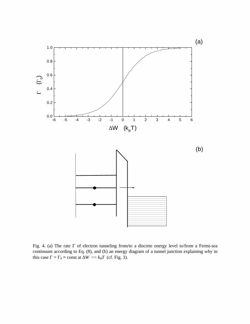
D:\Likharev\Nano\Reviews\ProcIEEE\Full0599.doc 41
Fig. 4. (a) The rate Γ of electron tunneling from/to a discrete energy level to/from a Fermi-seacontinuum according to Eq. (8), and (b) an energy diagram of a tunnel junction explaining why inthis case Γ = Γ0 ≈ const at ∆W >> kBT (cf. Fig. 3).
-6 -5 -4 -3 -2 -1 0 1 2 3 4 5 60.0
0.2
0.4
0.6
0.8
1.0
(b)
(a)Γ
(Γ
0)
∆W (kBT)

D:\Likharev\Nano\Reviews\ProcIEEE\Full0599.doc 42
(a)tunnelbarrier
source gate electrodeelectrode Q=-ne
C0 Usmallisland
(b) Qe - ne
- + - + U - + - + - + - + - + - +
-Qe
Fig. 5. Single-electron box: (a) schematics, (b) a particular geometry in which the "externalcharge" Qe = C0U can be readily visualized, and (c) the "Coulomb staircase", i.e. the step-likedependence of the average charge Q = -ne on the gate voltage, for several values of temperature.
-1 0 1 2-1
0
1
2k
BT/E
c = 0
0.03 0.01
(c)
Ave
rage
Cha
rge
<Q
> (
e)
"External Charge" Qe = C
0U (e)

D:\Likharev\Nano\Reviews\ProcIEEE\Full0599.doc 43
(a)U
gate
-V/2 +V/2 I(t)
source drain
(c)V
e/CΣ
n = -1 n= +1
0 Qe
-3e/2 -e/2 +e/2 3e/2
n = 0
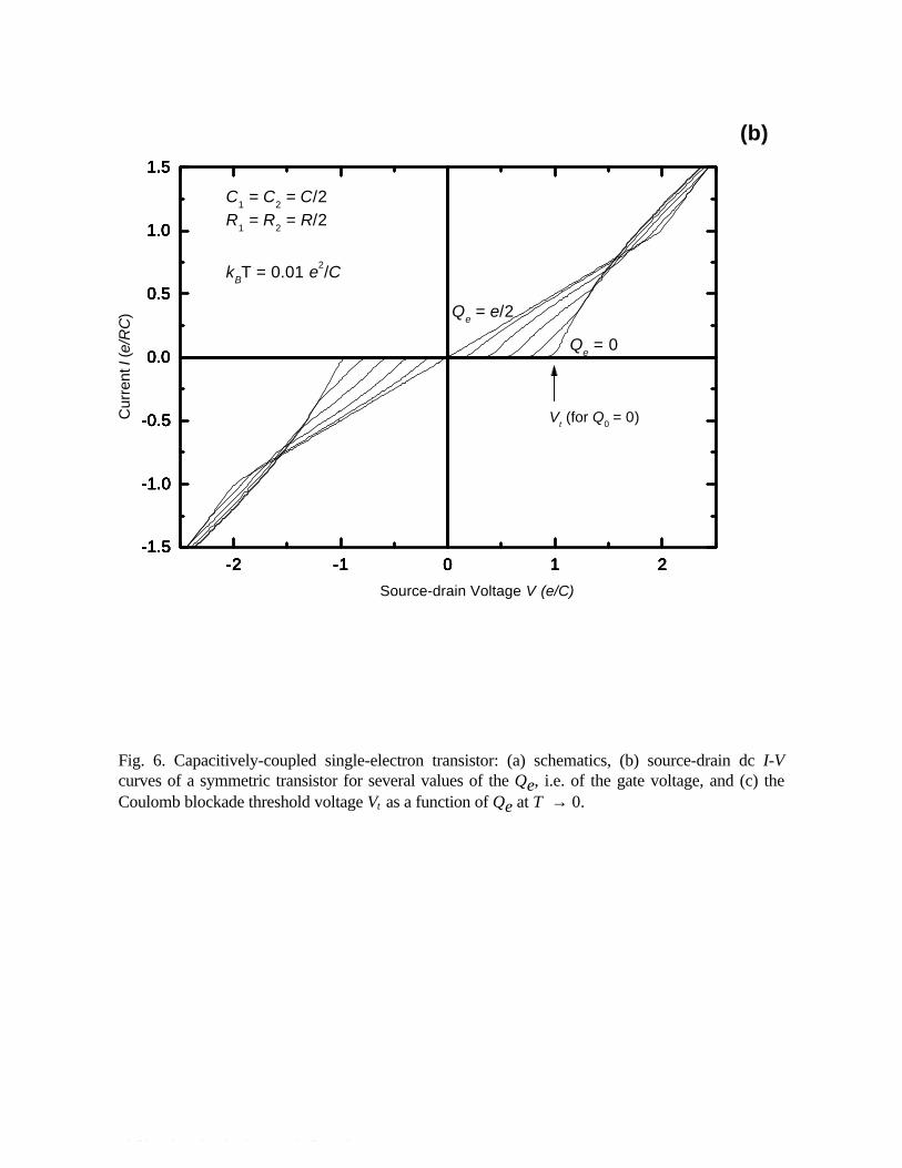
D:\Likharev\Nano\Reviews\ProcIEEE\Full0599.doc 44
Fig. 6. Capacitively-coupled single-electron transistor: (a) schematics, (b) source-drain dc I-Vcurves of a symmetric transistor for several values of the Qe, i.e. of the gate voltage, and (c) theCoulomb blockade threshold voltage Vt as a function of Qe at T → 0.
-2 -1 0 1 2-1.5
-1.0
-0.5
0.0
0.5
1.0
1.5
Vt (for Q0 = 0)
Qe = 0
Qe = e/2
C1 = C
2 = C/2
R1 = R
2 = R/2
kBT = 0.01 e2/C
-2 -1 0 1 2-1.5
-1.0
-0.5
0.0
0.5
1.0
1.5
-2 -1 0 1 2-1.5
-1.0
-0.5
0.0
0.5
1.0
1.5
-2 -1 0 1 2-1.5
-1.0
-0.5
0.0
0.5
1.0
1.5
-2 -1 0 1 2-1.5
-1.0
-0.5
0.0
0.5
1.0
1.5
Cur
rent
I (e
/RC
)
-2 -1 0 1 2-1.5
-1.0
-0.5
0.0
0.5
1.0
1.5
Source-drain Voltage V (e/C)
(b)
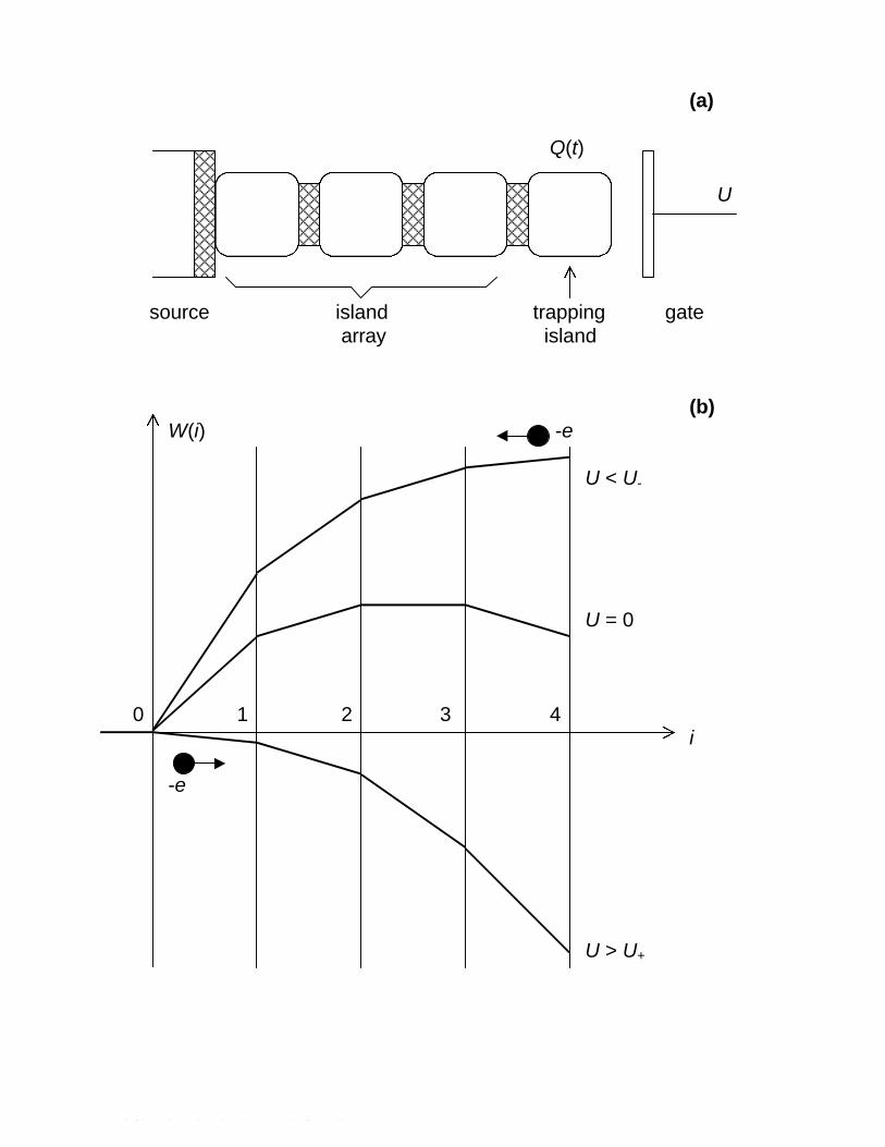
D:\Likharev\Nano\Reviews\ProcIEEE\Full0599.doc 45
(a)
Q(t)
U
source island trapping gate array island
(b)W(i) -e
U < U-
U = 0
0 1 2 3 4i
-e
U > U+

D:\Likharev\Nano\Reviews\ProcIEEE\Full0599.doc 46
(c) n
n = 2
n = 1
n = 0
U- 0 U+ U
Fig. 7. Single-electron trap: (a) schematics, (b) electrostatic energy of an extra electron as afunction of its position for three values of the gate voltage U, and (c) the static characteristic of thedevice (at T → 0).

D:\Likharev\Nano\Reviews\ProcIEEE\Full0599.doc 47
(a)
U(t)gate
-V/2 +V/2
source drain
(b)U1(t) U2(t) U3(t) U4(t) U5(t)
source drain
(c)
5 54
Ui(t) 3 2 1
i
0 t
Fig. 8. Single-electron (a) turnstile and (b) pump; (c): a possible set of waveforms applied to thepump gates.

D:\Likharev\Nano\Reviews\ProcIEEE\Full0599.doc 48
(a)tunneljunction (C, R)
Q(t)
I(t) V
resistor (Rs)
(b) Q(t)
+e/2
0 t
-e/2
∆t = e/<I>
Fig. 9. The simplest single-electron oscillator: (a) schematics and (b) typical dynamics of the tunneljunction charge.
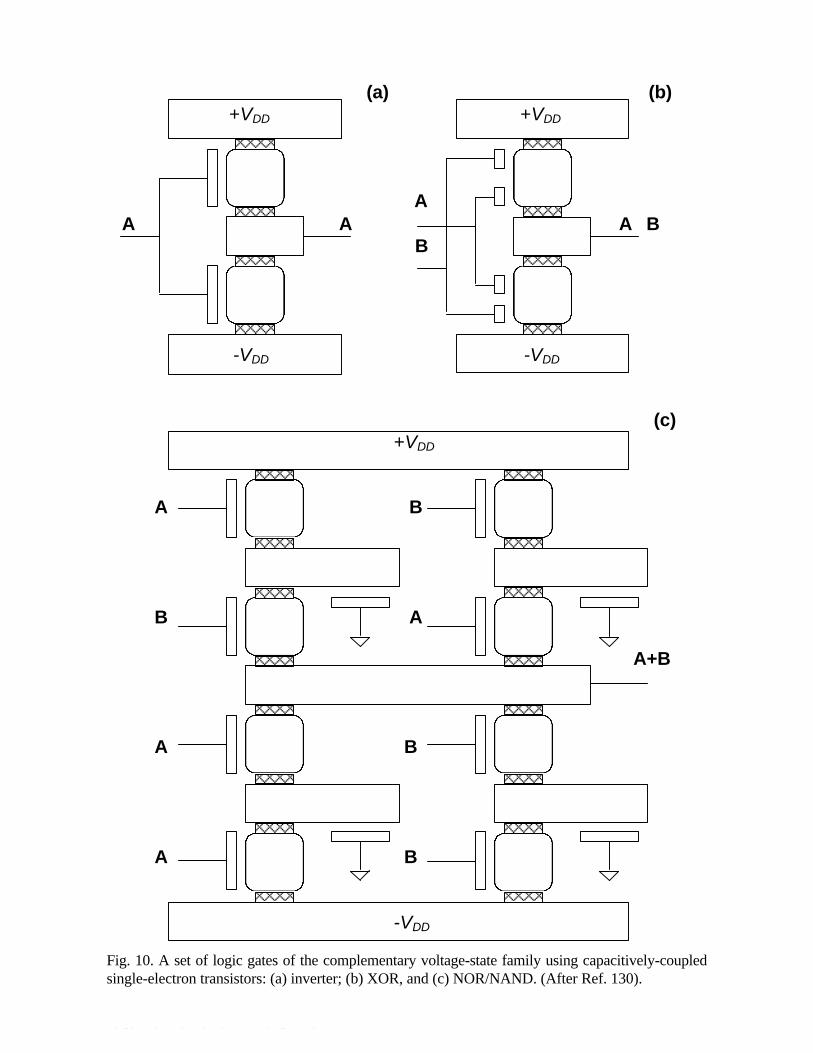
D:\Likharev\Nano\Reviews\ProcIEEE\Full0599.doc 49
(a) (b) +VDD +VDD
A A A A⊕B
B
-VDD -VDD
(c)+VDD
A B
B A
A+B
A B
A B
-VDD
Fig. 10. A set of logic gates of the complementary voltage-state family using capacitively-coupledsingle-electron transistors: (a) inverter; (b) XOR, and (c) NOR/NAND. (After Ref. 130).
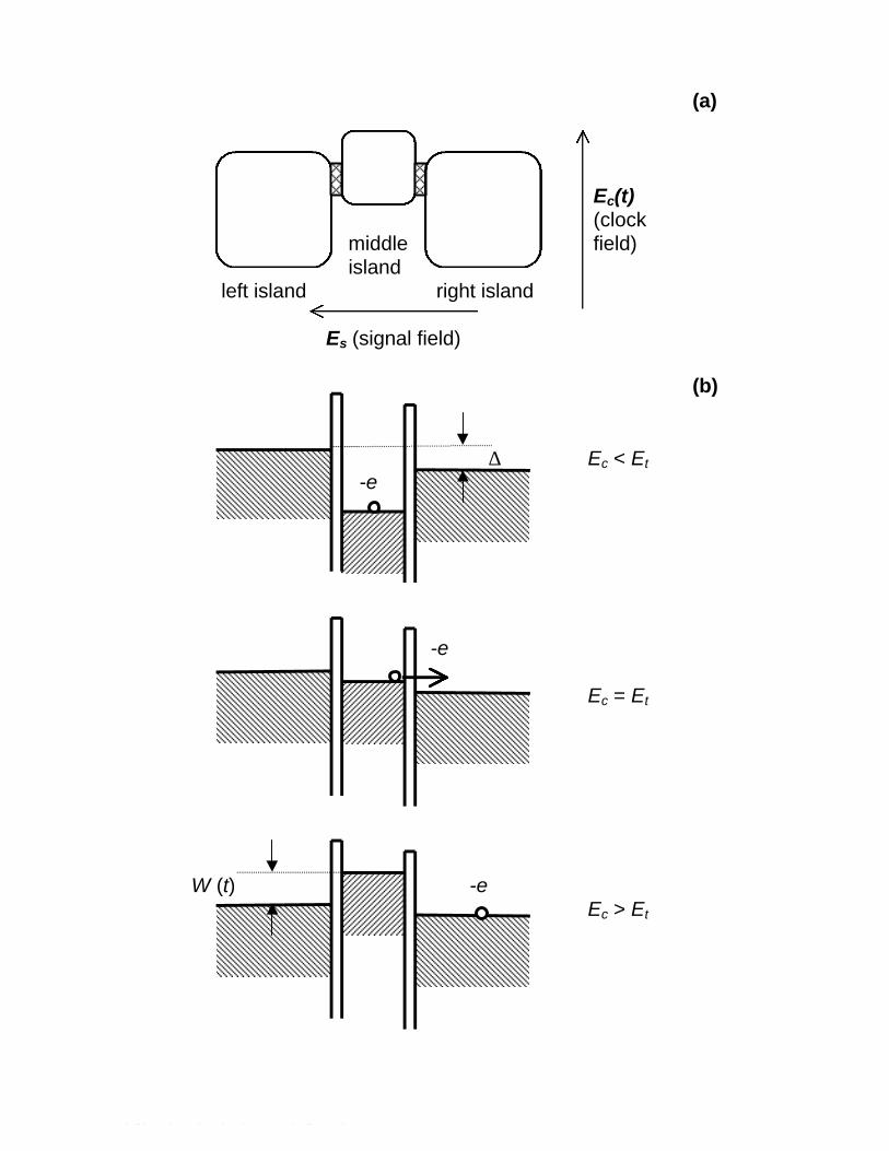
D:\Likharev\Nano\Reviews\ProcIEEE\Full0599.doc 50
(a)
Ec(t) (clock
middle field) island
left island right island
Es (signal field)
(b)
∆ Ec < Et
-e
-e
Ec = Et
W (t) -eEc > Et

D:\Likharev\Nano\Reviews\ProcIEEE\Full0599.doc 51
(c)
+
z
x
z
y
-
+
+- -
Phase 1
Phase 2
Phase 3OFF ON
OFF ON
State ON
State ON
State OFF
State OFF
Phase 4
Phase 5
Phase 6
+-
State OFF
Phase 1
-
-
-
-
1
+
0
1
-
0+
-
E (t)E (t) E(t)
E = const
c c
b
+-
-
+-
-
+
+
-
Fig. 11. SET Parametron: (a) schematics and (b) energy diagram at 3 values of the clock fieldEc(t). Energy difference ∆ between the edge islands is proportional to the signal field Es, while theenergy shift W(t) of the middle island is determined by the clock field. (c) Shift register using avariety of SET Parametron cells ("single-exciton parametrons") which do not require the initialcharging. (After Ref. 142).

D:\Likharev\Nano\Reviews\ProcIEEE\Full0599.doc 52
gate
- + - +source - + - + drain
- + - + - - - -
+q (q ~ e) single charged impurity
induced surface charge -q' (q'~ q)
Fig. 12. The effect of a single charged impurity on the single-electron transistor.

D:\Likharev\Nano\Reviews\ProcIEEE\Full0599.doc 53
(a)
0.0 0.2 0.4 0.6 0.8 1.0
0
1
2
3
4
5
6
V t/V t,0
C0= 0
N=5
N=10
N=15
N=20
N=4N=3
N=2Pro
babi
lity
dens
ity
(b)
0.0 0.2 0.4 0.6 0.8 1.00
1
2
3
4
5
6
H/H0
Pro
bab
ilit
y d
e nsi
ty
C0=0
N=5
N=10
N=15
N=20
N=4
N=3N=2
Fig. 13. Histograms of (a) Coulomb blockade threshold voltage Vt, and (b) energy barrier height Hfor statistical ensembles of 1D single-electron arrays with N tunnel barriers and randombackground charges of islands. Index 0 corresponds to the values of Vt and H in the absence ofbackground charges. All the junction capacitances C are assumed equal, stray capacitancesnegligibly small. Figure courtesy of Dr. A. Korotkov (unpublished).


Full0599.doc
Vb + Vr Vb - Vr (a)
VW word line
crestedfloating barrier (b)gate
single-electron
transistor SET islands
bit bit floating line + line - gates
transistor islands
next word cell
bit line + bit line - next bit cell read output
10 nm
FET sense amplifier
Fig. 14. Hybrid SET/FET memory insensitive to the background charge randomness: (a) schematics, and (b) side view on a possible layout compatiblewith room-temperature operation and a density of 100 Gbits/cm2. (After Ref. 164.)
word line
crested barrier

Full0599.doc
U
eV
(a) (b)
j
(c) (d)
U
eVj
U
(e) (f)
j
d
d
d' d'
d
U'
eV
Fig. 15. Various tunnel barriers without (left column) and with (right column) applied electric field:(a, b) Usual uniform barrier (often called "rectangular" or "trapezoidal"). (c, d) Crested barrier withparabolic profile. (e, f) Trilayer crested barrier. (After Ref. 167.)

D:\Likharev\Nano\Reviews\ProcIEEE\Full0599.doc 57
Fig. 16. Tunnel current (solid lines) and floating gate recharging time scale (dashed lines) for usualrectangular barriers with two values of thickness d (open points), and for a crested parabolic barriershown in Fig. 15c,d (solid points). In all cases the maximum height of the barrier U = 3.2 V, andthe electron effective mass under the barrier is m = 0.3m0 (the parameters correspond to a SiO2
barrier between n+-doped silicon electrodes. (After Ref. 167.)
0 2 4 6 8 10 1210-10
10-7
10-4
10-1
102
105
108
10-10
10-7
10-4
10-1
102
105
108
12 nm8 nm
Crested parabolicbarrier d = 15 nm
Uniform barrierd = 12 nm
Uniform barrierd = 8 nm
Rec
hrgi
ng T
ime
(s)
Tun
nel C
urre
nt D
ensi
ty (
A/m
2 )
Voltage (Volts)
0 2 4 6 8 10 1210-10
10-7
10-4
10-1
102
105
108
10-10
10-7
10-4
10-1
102
105
108
Rec
hrgi
ng T
ime
(s)
Tun
nel C
urre
nt D
ensi
ty (
A/m
2 )
Voltage (Volts)
0 2 4 6 8 10 1210-10
10-7
10-4
10-1
102
105
108
10-10
10-7
10-4
10-1
102
105
108
Rec
hrgi
ng T
ime
(s)
Tun
nel C
urre
nt D
ensi
ty (
A/m
2 )
Voltage (Volts)
0 2 4 6 8 10 1210-10
10-7
10-4
10-1
102
105
108
10-10
10-7
10-4
10-1
102
105
108
Rec
hrgi
ng T
ime
(s)
Tun
nel C
urre
nt D
ensi
ty (
A/m
2 )
Voltage (Volts)
0 2 4 6 8 10 1210-10
10-7
10-4
10-1
102
105
108
10-10
10-7
10-4
10-1
102
105
108
Rec
hrgi
ng T
ime
(s)
Tun
nel C
urre
nt D
ensi
ty (
A/m
2 )
Voltage (Volts)
0 2 4 6 8 10 1210-10
10-7
10-4
10-1
102
105
108
10-10
10-7
10-4
10-1
102
105
108
Rec
hrgi
ng T
ime
(s)
Tun
nel C
urre
nt D
ensi
ty (
A/m
2 )
Voltage (Volts)

D:\Likharev\Nano\Reviews\ProcIEEE\Full0599.doc 58
(a)
(b)
Fig. 17. Dual-gate n-MOSFET with ballistic transfer of electrons along an undoped channel: (a) asimple geometric model, (b) conduction band edge diagram (schematically), and (c) subthresholdcharacteristics as calculated using a simple semi-analytical model [170]. Contact doping 3×10²⁰
cm-3, other parameters: 2s = 1.5 nm, d - s = 2.5 nm; source drain voltage is close to 0.5 V. Finehatching shows the parameter window where the gate leakage exceeds the source current, whilecoarse hatching shows the window where the holes cannot be ignored (in both regions, largedeviations from the calculation results are expected).
Title:fig1.figCreator:fig2dev Version 3.1 Patchlevel 2Preview:This EPS picture was not savedwith a preview included in it.Comment:This EPS picture will print to aPostScript printer, but not toother types of printers.
Full0599.doc
Fig. 18. A cartoon showing the operation principle of Hitachi's memory cell. A single electroncaptured in a silicon grain may block transfer of electrons along a percolation current path.(Courtesy of Dr. T. Ishii).

Full0599.doc
(a)
(b)
Fig. 19. Floating gate memory cell developed at the University of Minnesota: (a) schematics and(b) SEM picture taken before the control gate deposition. (After Ref. 175.)
Source
Drain
Substrate
Polysilicon ControlGate Polysilicon Dot
SiliconChannel
SubstrateBuried Oxide
Buried Oxide
Polysilicon Dot
Silicon Channel

D:\Likharev\Nano\Reviews\ProcIEEE\Full0599.doc 61
* 300 K NOVORAM
*77 K
SET-FET 40 K
HYBRIDS
*10K
FET DRAM (SIA Forecast) ??
1 3 10 30 100 300Minimum Feature Size (nm)
Fig. 20. Scaling prospects for various bit-addressable memories. Solid lines show the estimatedrelation between the minimum feature size and integration scale. The bit density is recalculated tothe integration scale using the log-linear extrapolation of the chip size growth, similar to thataccepted in the SIA forecast [177]. The DRAM projections (the lower right line) are also borrowedfrom that forecast. Dashed lines shows the regions where I anticipate major problems to occur (onthe top of fabrication challenges). Dotted line shows the range where the operation of the SET/FEThybrid memory is possible at low temperatures (indicated with numbers at the dots).
256T
64T
16T
4T
1T
256G
64G
16G
4G
1G

D:\Likharev\Nano\Reviews\ProcIEEE\Full0599.doc 62
V + V V - VW R W R
FET
SET
amplifierload load
READ/WRITEhead (tip)
moving substrate
conducting ground layer
tunnelbarrier
chargedgrains
crested
Fig. 21. Proposed electrostatic data storage system with hybrid SET/FET readout. (After Ref. 178.)


![Electric Circuits and Electron Devices[1]](https://static.fdocuments.in/doc/165x107/577d221f1a28ab4e1e969e8b/electric-circuits-and-electron-devices1.jpg)