
Silicon Semiconductor Issue 5 2020
40
inside News Review, News Analysis, Features, Research Review, and much more... Free Weekly E News round up go to: www.siliconsemiconductor.net Real-time analysis in electric grids SONOTEC launches contactless IC sensors Covid 19 and the semiconductor industry View on the logic technology roadmap The Automated Atomic Force Microscope for ultra large and heavy flat panel displays By Volume 41 Issue V 2020 @siliconsemi www.siliconsemiconductor.net Modules Interrogated Acoustically
Transcript of Silicon Semiconductor Issue 5 2020

inside News Review, News Analysis, Features, Research Review, and much more...Free Weekly E News round up go to: www.siliconsemiconductor.net
Real-time analysis in electric grids
SONOTEC launches contactless IC sensors
Covid 19 and the semiconductor industry
View on the logic technology roadmap
The Automated Atomic Force Microscope for ultra large and heavy flat panel displaysBy
Volume 41 Issue V 2020 @siliconsemi www.siliconsemiconductor.net
Modules Interrogated Acoustically
Front Cover v5.indd 1Front Cover v5.indd 1 03/12/2020 12:4203/12/2020 12:42

GET IN TOUCH to discuss your manufacturing needswww.EVGroup.com EVG® LITHOSCALE®
Featuring next-generation digital lithography technology for high-volume manufacturing
Combining high resolution with powerful digital processing to enable next-generation heterogeneous integration applications
Scalable solution accommodating R&D and HVM needs in one system without adding on footprint
Addressing lithography needs for Advanced Packaging, MEMS, Biomedical and High-density PCB applications
LITHOSCALE LITHOSCALE®
LITHOSCALE®MLE™ Maskless Exposure
Lithography System
Untitled-5 1Untitled-5 1 16/09/2020 16:1716/09/2020 16:17

editor’sviewBy Mark Andrews, Technical Editor
COPYRIGHT SILICON SEMICONDUCTOR l ISSUE V 2020 l WWW.SILICONSEMICONDUCTOR.NET 3
Silicon Semiconductor is published four times a year on a controlled circulation basis. Non-qualifying individuals can subscribe at: £50.00/e60.00 pa (UK & Europe), £70.00 pa (air mail), $90.00 pa (USA). Cover price £4.50. All information herein is believed to be correct at time of going to press. The publisher does not accept responsibility for any errors and omissions. The views expressed in this publication are not necessarily those of the publisher. Every effort has been made to obtain copyright permission for the material contained in this publication. Angel Business Communications Ltd will be happy to acknowledge any copyright oversights in a subsequent issue of the publication. Angel Business Communications Ltd © Copyright 2020. All rights reserved. Contents may not be reproduced in whole or part without the written consent of the publishers. The paper used within this magazine is produced by chain of custody certified manufacturers, guaranteeing sustainable sourcing. US mailing information: Silicon Semiconductor, ISSN 1096-598X, is published 4 times a year, Jan/Feb, March, April/May, June, July, August/September, October, November/ December by Angel Business Communications Ltd, Unit 6, Bow Court, Fletchworth Gate, Burnsall Rd, Coventry CV5 6SP. UK. The 2020 US annual subscription price is $90.00. Airfreight and mailing in the USA by agent named World Container Inc, 150-15, 183rd Street, Jamaica, NY 11413, USA. Periodicals postage paid at Brooklyn, NY 11256. US Postmaster: Send address changes to Compound Semiconductor, Air Business Ltd, c/o WN Shipping USA, 156-15, 146th Avenue, 2nd Floor, Jamaica, NY 11434, USA. Printed by: The Manson Group. ISSN 2050-7798 (Print) ISSN 2050-7801 (Online) © Copyright 2020.
We strive for accuracy in all we publish; readers and contributors are encouraged to contact us if they recognise an error or omission. Once a magazine edition is published [online, in print or both], we do not update previously published articles to align old company names, branding, marketing efforts, taglines, mission statements or other promotional verbiage, im-ages, or logos to newly created or updated names, images, typographic renderings, logos (or similar) when such references/images were accurately stated, rendered or displayed at the time of the original publication. When companies change their names or the images/text used to represent the company, we invite organizations to provide Angel Business Communications with a news release detailing their new business objectives and/or other changes that could impact how customers/prospects might recognise the company, contact the organisa-tion, or engage with them for future commercial enterprise.
Publisher & Editor Jackie Cannon [email protected] +44 (0)1923 690205Technical Editor Mark Andrews [email protected] Sales & Marketing Manager Shehzad Munshi [email protected] +44 (0)1923 690215USA Representatives Tom Brun Brun Media [email protected] +001 724 539-2404 Janice Jenkins [email protected] +001 724-929-3550Director of Logistics Sharon Cowley [email protected] +44 (0)1923 690200Design & Production Manager Mitch Gaynor [email protected] +44 (0)1923 690214Circulation Director Scott Adams [email protected] +44 (0)2476 718970Chairman Stephen Whitehurst [email protected] +44 (0)2476 718970
Chief Executive Officer Sukhi Bhadal [email protected] +44 (0)2476 718970 Chief Technical Officer Scott Adams [email protected] +44 (0)2476 718970 Directors Jackie Cannon, Sharon Cowley
Published by Angel Business Communications Ltd, Unit 6, Bow Court, Fletchworth Gate, Burnsall Road, Coventry CV5 6SP, UK. T: +44 (0)2476 718 970 F: +44 (0)2476 718 971 E: [email protected]
THE YEAR OF THE UNEXPECTED has given us a pandemic, economic and social upheavals, heroic frontline workers and so many superlative situations it is challenging to note them all. Yet as 2020 winds down there is renewed hope for health – health from promising new COVID-19 vaccines, and economic health in the form of unexpectedly sharp growth in both IC and semiconductor equipment sales.
The SEMI trade group reported recently that while the world anxiously anticipates the benefits of COVID-19 vaccines, one could hardly tell that many global economic sectors struggled in 2020 if they ignored the big picture and focused instead on semiconductors. SEMI reported that chip sales rose a healthy 12 percent in September, marking a second consecutive month of double-digit growth. Yet these numbers pale compared to manufacturing equipment sales; the first nine months of 2020 saw 23.6 percent growth! Equipment sales look poised to beat the previous record of $64.5 billion set in 2018. Great Expectations, indeed.
The record growth of semiconductor equipment sales occurred largely in China, Taiwan and Korea. China leads since it has the most fabs under construction; SEMI projects this will make China the world’s largest capital equipment market for the first time. European and North American sales were down in 2020 thanks mostly to pandemic effects on automotive and factory automation sales, which are expected to rebound in 2021.
What is not surprising is the fact that pandemic inspired work-from-home product sales and other pandemic influenced
Amazing 4Q IC sales create ‘great expectations’ for 2021
purchasing drove chip sales ever higher for everything from air filtration systems to webcams.
In this issue of Silicon Semiconductor we explore advances in metrology for large panel devices made possible by the Park Systems NX-TSH AFM that includes ‘future proofing’ for panels larger than 75 inches. Edwards Vacuum provides insights into how its preventative maintenance programmes benefitted customers during COVID-19 surges.
We have two feature articles looking at different ways to use ultrasonics: inspection and defect analysis from Nordson’s SONOSCAN division and contactless chemical flow measurement from SONOTEC. We also take an in-depth look at how imec researchers envision roadmaps for leading-edge logic chip development.
Viewpoint v1.indd 3Viewpoint v1.indd 3 02/12/2020 15:2802/12/2020 15:28

4 WWW.SILICONSEMICONDUCTOR.NET l ISSUE V 2020 l COPYRIGHT SILICON SEMICONDUCTOR
VOLUME 41 ISSUE V 2020
CONTENTS
14 SONOTEC launches contactless metering for IC manufacturers SONOTEC is leveraging its decades of experience in pharmaceutical and other high reliability markets to bring contactless ultrasonic sensor monitoring to semiconductor manufacturers, delivering highly accurate systems designed to increase uptime and safety, all while conserving resources
18 KEEP CALM AND CARRY ON Covid 19 and the semiconductor industry We have all been challenged by the Covid-19 pandemic. As an essential part of an essential industry, Edwards has faced specific challenges in maintaining production and providing support to our customers
22 A view on the logic technology roadmap While chipmakers are moving ahead with technology generations, maintaining the same timeline for scaling transistors in the front-end-of-line (FEOL), contacts and interconnects in the middle- (MOL) and back-end-of-line (BEOL) has become challenging
32 Enabling the aggregation of real-time power quality analysis in electric grids Data analytics is a significant and emerging force in the digitalisation of electricity transmission grids that can empower grid operators with a deeper understanding and more precise control of their infrastructure
37 IGBT modules interrogated acoustically IGBT failures, because of the typically high voltage and power levels, can be both costly and dangerous. It makes sense to find internal structural defects be- fore they have an opportunity to go wrong
12 COVER STORY Park Systems overcomes 300mm barrier to measure ultra-large & heavy flat panel displays at nanoscale The atomic force microscope (AFM) experts at Park Systems have smashed through the 300mm limits of other metrology tools used to measure large and heavy flat panel displays with the development of its pioneering NX Tip Scan Head (NX-TSH) automated AFM system.
Contents SiS v1.indd 4Contents SiS v1.indd 4 02/12/2020 15:2502/12/2020 15:25

COPYRIGHT SILICON SEMICONDUCTOR l ISSUE V 2020 l WWW.SILICONSEMICONDUCTOR.NET 5
news06 IMT modernizes MEMS foundry services with plasma etch solution
07 EV GROUP addresses key process gap in heterogeneous integration
08 Dialog Semiconductor licenses its non-volatile resistive RAM technology to GLOBALFOUNDRIES
09 3D-Micromac unveils laser annealing system for magnetic sensor manufacturing
10 Deca announces chiplet advanced packaging partnership with ADTEC
11 Picosun’s medical ALD solution to safer surgeries
06
14 18
32 37
11
Contents SiS v1.indd 5Contents SiS v1.indd 5 02/12/2020 15:2502/12/2020 15:25

6 WWW.SILICONSEMICONDUCTOR.NET l ISSUE V 2020 l COPYRIGHT SILICON SEMICON DUCTOR
NEWS REVIEWsIMT modernizes MEMS foundry services with plasma etch solutionINNOVATIVE MICRO TECHNOLOGY (IMT), a global leader in the development and production of complex microelectromechanical systems (MEMS), today announced the purchase of an Omega Rapier plasma etch system from SPTS Technologies, a KLA company. The installation of the Rapier™ this month will put IMT at the cutting edge of MEMS and sensors manufacturing and extends development and production capability for its growing customer base in photonics, BioMEMS and sensors.
“The MEMS industry is experiencing a resurgence of growth driven by a proliferation of innovative new communications, sensing, and medical applications,” stated Eric Sigler, CEO of IMT. “SPTS Technologies is at the forefront of MEMS manufacturing with its deep reactive ion etch (DRIE) solutions, having been a co-developer and first licensee of the ‘Bosch Process’. The addition of the Rapier DRIE capability allows us to offer an industry-leading technology to our foundry customers while expanding capacity for future development and new applications. This investment exemplifies our commitment
to technical excellence, even in these uncertain times. SPTS has been working closely with the leading MEMS manufacturers, foundries and research institutes for more than two decades, achieving an install base of over 1300 DRIE modules,” stated David Butler, General Manager of SPTS Technologies. “The Rapier DRIE process module provides the high-level of profile control, selectivity and uniformity needed for the critical feature requirements of next generation MEMS devices. We are pleased to bring this important capability to IMT’s foundry environment and be part of their exciting 200mm technology portfolio.”
IMT is already the largest pure-play MEMS foundry in the United States. With the Rapier, IMT is able to achieve best-in-class control over side-wall profile, scalloping, and aspect ratio, plus world-class etch rates, uniformity, and tilt control. By integrating SPTS’s patented Claritas end-point technology, IMT can implement precise control of the Si etch to a stop layer as commonly used for MEMS processing. With the Rapier DRIE technology, IMT can better support its customers in the design, development,
and manufacturing of devices that require superior deep silicon etching and maximum process control for optimum performance.
IMT’s engineers will use industry-leading DRIE technology to improve throughput and yield in many types of devices including MEMS sensors and mirrors, photonics, microfluidic biochips, fiber blocks, lens arrays, silicon-optical benches and 3D interconnected devices using through-silicon vias (TSVs).
ULVAC Techno offers equipment support in Japan and East AsiaULVAC TECHNO is offering US and European-based vacuum companies a means of expanding their presence in Japan and East Asia, by providing companies customer support, including maintenance of vacuum equipment, parts and supplies.
ULVAC Techno has a long history and experience in installing, repairing and maintaining vacuum-based process equipment and is now actively engaged in business partnerships with US and European-based companies. Its services include vacuum equipment repair, vacuum equipment relocation, installation, vacuum equipment improvement and modifications, parts sales, parts recycling and cleaning, surface treatment and used equipment sales. In order to efficiently provide these services to customers, there are 27 locations in Japan with 330 service engineers available 24 hours a day.
The company was established in 1979 and is a subsidiary of ULVAC, Inc, with a main office is located Cigasaki City, Kanagawa Prefecture, Japan. The ULVAC Group has 66 offices in 13 countries and regions around the world - focusing
on semiconductors, as well as electronic devices, flat panel displays, organic EL displays, solar cells, automobiles, chemicals, pharmaceuticals, food and metal industries.
News SiS v1.indd 6News SiS v1.indd 6 02/12/2020 15:2702/12/2020 15:27

COPYRIGHT SILICON SEMICONDUCTOR l ISSUE V 2020 l WWW.SILICONSEMICONDUCTOR.NET 7
NEWS REVIEW sEV GROUP addresses key process gap in heterogeneous integrationEV GROUP (EVG), a supplier of wafer bonding and lithography equipment for the MEMS, nanotechnology, and semiconductor markets, has announced that it has successfully demonstrated a complete process flow for collective die-to-wafer (D2W) hybrid and fusion bonding with sub-two-micron placement accuracy utilizing existing EVG wafer bonding technology and processes, as well as existing bond interface materials. This breakthrough, which was demonstrated at EVG’s Heterogeneous Integration Competence Centre, represents an important milestone in accelerating the deployment of heterogeneous integration (HI) in next-generation 2.5D and 3D semiconductor packaging.
Located at EVG’s headquarters, the Heterogeneous Integration Competence Centre offers consultancy services, feasibility studies and demonstrations, process development support and pilot-production services. Serving as an open access innovation incubator, it is designed to help customers accelerate technology development, minimize risk, and develop differentiating technologies and products through HI/advanced packaging all while guaranteeing the highest IP protection standards that are required for working on pre-release products. All process and integration aspects of both wafer-to-wafer and different D2W integration approaches are focus technologies at the centre.
EV Group successfully demonstrated a complete process flow for collective D2W hybrid and fusion bonding with sub-two-micron placement accuracy. Shown here: individual dies on a wafer after collective D2W bonding.
Leading-edge applications such as artificial intelligence, autonomous driving, augmented/virtual reality and 5G all require the development of high-bandwidth, high-performance and low-power-consumption devices without increasing production cost. As traditional 2D silicon scaling reaches its cost limits, the semiconductor industry is turning to
HI – the manufacturing, assembly and packaging of multiple different components or dies with different feature sizes and materials onto a single device or package – in order to increase performance on new device generations. Collective D2W bonding is an essential HI process step that enables functional layer and known good die (KGD) transfer to support cost-efficient manufacturing of new types of 3D-ICs, chiplets, and segmented and 3D system on chip (SoC) devices.
“For more than 20 years, EVG has provided process solutions and expertise to support the advancement of HI, including D2W bonding, where our technology has been successfully implemented in high-volume manufacturing applications,” stated Markus Wimplinger, corporate technology development & IP director for EV Group.
“Our Heterogeneous Integration Competence Center, which is supported by our worldwide network of process technology teams, enhances our capabilities in this critical area by providing a foundation for customers and partners working with EVG to develop new 3D/HI solutions and products. Among these is our new
collective D2W bonding approach, where we have demonstrated the ability to perform all key process steps in-house with high placement accuracy and transfer rate using our existing wafer bonding and debonding, metrology and cleaning process equipment along with select third-party systems from our development partners. We’d like to thank our partners for their role and support in enabling this important achievement. A special thanks goes to IRT Nanoelec and CEA-Leti, which both provided the substrates that were used in this demonstration.”
Results of the Collective Die-to-Wafer Bonding Demonstration
A technical paper highlighting the results of EVG’s collective D2W bonding process was presented at the Electrochemical Society (ECS) PRiME 2020 Conference earlier this month and can be downloaded from the ECS PRiME website at:https://ecs.confex.com/ecs/prime2020/meetingapp.cgi/Paper/142631 (registration required).
For more information on EVG’s hybrid and fusion bonding solutions, visit https://www.evgroup.com/technologies/fusion-and-hybrid-bonding
News SiS v1.indd 7News SiS v1.indd 7 02/12/2020 15:2702/12/2020 15:27

8 WWW.SILICONSEMICONDUCTOR.NET l ISSUE V 2020 l COPYRIGHT SILICON SEMICON DUCTOR
NEWS REVIEWsDialog Semiconductor licenses its non-volatile resistive RAM technology to GLOBALFOUNDRIESDIALOG SEMICONDUCTOR a provider of battery and power management, Wi-Fi and Bluetooth low energy (BLE) and Industrial edge computing solutions and GLOBALFOUNDRIES, the world’s leading specialty foundry, today announced that they have entered into an agreement in which Dialog licenses its Conductive Bridging RAM (CBRAM) technology to GLOBALFOUNDRIES. The resistive ram (ReRAM)-based technology was pioneered by Adesto Technologies which was recently acquired by Dialog Semiconductor in 2020. GLOBALFOUNDRIES will first offer Dialog’s CBRAM as an embedded, non-volatile memory (NVM) option on its 22FDX platform, with the plan to extend to other platforms.
Dialog’s proprietary and production proven CBRAM technology is a low power NVM solution designed to enable
a range of applications from IoT and 5G connectivity to artificial intelligence (AI). Low power consumption, high read/write speeds, reduced manufacturing costs and tolerance for harsh environments make CBRAM particularly suitable for consumer, medical, and select industrial and automotive applications. Furthermore, CBRAM technology enables cost-effective embedded NVM for advanced technology nodes required for products in these markets.
“CBRAM is one of Adesto’s marquee memory technologies and a game-changing addition to Dialog’s portfolio. This new licensing partnership with GLOBALFOUNDRIES speaks to just how quickly Dialog and Adesto have hit the ground running together,” said Mark Tyndall, Senior Vice President of Corporate Development and General Manager of the Industrial Mixed
Signal Business Group at Dialog Semiconductor.
Overcoming the integration and reliability challenges often associated with ReRAM, Dialog’s CBRAM technology offers a reliable low-cost embedded memory while maintaining ReRAMs low voltage operation. This translates to lower energy write and read access as compared to standard embedded Flash offerings.
CBRAM will be available in production for use by GF customers as an embedded NVM option on its 22FDX platform in 2022.Through IP customization, customers may modify the CBRAM cell to optimize their SoC designs, enhance security, or even adapt the cell for new applications. Additionally, CBRAM being a “back-end-of-line” technology enables relatively easy integration into other technology nodes.
News SiS v1.indd 8News SiS v1.indd 8 02/12/2020 15:2702/12/2020 15:27

COPYRIGHT SILICON SEMICONDUCTOR l ISSUE V 2020 l WWW.SILICONSEMICONDUCTOR.NET 9
NEWS REVIEW s3D-Micromac unveils laser annealing system for magnetic sensor manufacturingMICROMAC AG, supplier of laser micromachining and roll-to-roll laser systems for the semiconductor, photovoltaic, medical device and electronics markets, has introduced the first industrial selective laser annealing system for magnetic sensor formation – the microVEGA xMR. Incorporating a highly flexible, high-throughput tool configuration with on-the-fly spot and variable laser energy, the microVEGA xMR accommodates both Giant Magnetoresistance (GMR) and Tunnel Magnetoresistance (TMR) sensors, as well as easily adjusts magnetic orientation, sensor position and sensor dimension—making it an ideal solution for magnetic sensor production.
Crocus Technology, a leading manufacturer of innovative XtremeSense TMR magnetic sensors, has purchased and installed a microVEGA xMR system in its facility in Santa Clara, Calif., where the tool will be used in the production of its TMR sensors utilized in consumer electronics, industrial and Internet of Things (IoT) applications.
The magnetic sensor device market is experiencing strong growth driven by increased demand for magnetic sensors in consumer electronics such as rotation sensors and e-compasses in smartphones and wearables, in appliances such as linear position sensors and angle sensors for brushless DC motors, and in automotive applications such as power steering angle detection and electronic throttle control. Market research and consulting firm MarketsandMarkets estimates that the magnetic sensor market will grow from USD 4.3 billion in 2020 to USD 6.2 billion in 2025—a compound annual growth rate of 7.7 percent.
Thermal annealing has traditionally been used to maximize the magnetoresistance effects of GMR and TMR sensors. However, this approach requires multiple process steps to produce sensors with different magnetic orientations that are mounted in multi-chip packages or processed as integrated monolithic packages. New approaches are needed to reduce these process steps, simplify the overall production flow, provide scalability to smaller footprint, and enable more cost-effective production of integrated monolithic sensor packages.
“The microVEGA xMR from 3D-Micromac provides us with a flexible yet robust approach to integrated magnetic sensor formation that enables us to implement new sensor designs, lower our production cost and scale up to production more quickly. We want to thank 3D-Micromac for their end-to-end support on this new tool, including providing us with access to their process development and contract manufacturing services prior to tool installation. We look forward to continuing our work with them on new technology collaborations,” stated Zack Deiri, president and CEO, Crocus Technology.
The microVEGA xMR provides several advantages over thermal annealing for magnetic sensor manufacturing. These include higher precision to enable the processing of smaller magnetic device structures, which results in more devices per wafer, as well as the ability to set different reference magnetization directions on sensors across a single wafer.
The system’s on-the-fly spot and variable laser energy provide selective heating of the pinning layer in each sensor to “imprint” the intended magnetic orientation. Magnetic field strength and orientation is adjustable by recipe, while high-temperature gradients ensure low thermal impact.
This allows sensors to be processed directly next to read-out electronics as well as closer together, and enables the production of smaller sensors – freeing up space for processing more devices per wafer. The result is reduced process steps, simplified production flow, higher yield, and more cost-effective production of integrated monolithic sensor packages.
“Our microVEGA xMR system represents an important achievement in 3D-Micromac’s ongoing strategy to target future-oriented, high-growth-potential markets with innovative
products backed by our process expertise and applications services,” stated Tino Petsch, CEO, 3D-Micromac.
“We are pleased to have had the opportunity to work with Crocus Technology on one of the first installations of this new product, where they were able to take advantage of our wide range of services, including application and process development as well as contract manufacturing,
in order to accelerate their path to production for their new
sensor products.”
News SiS v1.indd 9News SiS v1.indd 9 02/12/2020 15:2702/12/2020 15:27
10 WWW.SILICONSEMICONDUCTOR.NET l ISSUE V 2020 l COPYRIGHT SILICON SEMICON DUCTOR
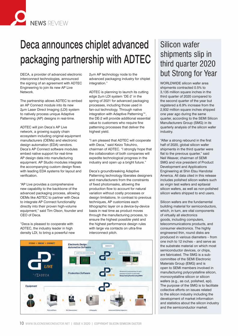
NEWS REVIEWsDeca announces chiplet advanced packaging partnership with ADTECDECA, a provider of advanced electronic interconnect technologies, announced the signing of an agreement with ADTEC Engineering to join its new AP Live Network.
The partnership allows ADTEC to embed an AP Connect module into its new 2µm Laser Direct Imaging (LDI) system to natively process unique Adaptive Patterning (AP) designs in real-time.
ADTEC will join Deca’s AP Live network, a growing supply chain ecosystem including original equipment manufacturers (OEMs) and electronic design automation (EDA) vendors. Deca’s AP Connect software modules embed native support for real-time AP design data into manufacturing equipment. AP Studio modules integrate the accompanying custom design flows with leading EDA systems for layout and verification.
“AP Live provides a comprehensive new capability to the backbone of the advanced packaging process, allowing OEMs like ADTEC to partner with Deca to integrate AP Connect functionality directly into their proven high-volume equipment,” said Tim Olson, founder and CEO of Deca.
“Deca is pleased to cooperate with ADTEC, the industry leader in high density LDI, to bring a powerful new
2µm AP technology node to the advanced packaging industry for chiplet integration.”
ADTEC is planning to launch its cutting edge 2µm LDI system ‘DE-2’ in the spring of 2021 for advanced packaging processes, including those used in fan-out technology. Through native integration with Adaptive Patterning™, the DE-2 will provide additional essential value to customers who require fine patterning processes that deliver the highest yield.
“I am pleased that ADTEC will cooperate with Deca,” said Keizo Tokuhiro, chairman of ADTEC. “I strongly hope that the collaboration of both companies will expedite technological progress in the industry and open up a bright future.”
Deca’s groundbreaking Adaptive Patterning technology liberates designers and manufacturers from the constraints of fixed photomasks, allowing the production flow to account for natural variation without costly processes or design limitations. In contrast to previous techniques, AP customizes each lithographic layer on a device-by-device basis in real time as product moves through the manufacturing process, to ensure the highest possible yield and the highest performance design rules with large via contacts on ultra-fine interconnect pitch.
Silicon wafer shipments slip in third quarter 2020 but Strong for YearWORLDWIDE silicon wafer area shipments contracted 0.5% to 3,135 million square inches in the third quarter of 2020 compared to the second quarter of the year but registered a 6.9% increase from the 2,932 million square inches shipped one year ago during the same quarter, according to the SEMI Silicon Manufacturers Group (SMG) in its quarterly analysis of the silicon wafer industry.
“After a strong rebound in the first half of 2020, global silicon wafer shipments in the third quarter were flat to the previous quarter,” said Neil Weaver, chairman of SEMI SMG and vice president of Product Development and Applications Engineering at Shin Etsu Handotai America. All data cited in this release includes polished silicon wafers such as virgin test wafers and epitaxial silicon wafers, as well as non-polished silicon wafers shipped to end users.
Silicon wafers are the fundamental building material for semiconductors, which, in turn, are vital components of virtually all electronics goods, including computers, telecommunications products, and consumer electronics. The highly engineered thin, round disks are produced in various diameters – from one inch to 12 inches – and serve as the substrate material on which most semiconductor devices, or chips, are fabricated. The SMG is a sub-committee of the SEMI Electronic Materials Group (EMG) and is open to SEMI members involved in manufacturing polycrystalline silicon, monocrystalline silicon or silicon wafers (e.g., as cut, polished, epi). The purpose of the SMG is to facilitate collective efforts on issues related to the silicon industry including the development of market information and statistics about the silicon industry and the semiconductor market.
News SiS v1.indd 10News SiS v1.indd 10 02/12/2020 15:2702/12/2020 15:27

COPYRIGHT SILICON SEMICONDUCTOR l ISSUE V 2020 l WWW.SILICONSEMICONDUCTOR.NET 11
NEWS REVIEW s
ACM Research enters 3D TSV copper plating marketACM RESEARCH, a supplier of wafer processing solutions for semiconductor and advanced wafer-level packaging (WLP) applications, today introduced its Ultra ECP 3d platform for conformally filled 3D through-silicon via (TSV) applications. Leveraging ACM’s Ultra ECP ap and map platforms, the Ultra ECP 3d platform delivers high-performance copper (Cu) electroplating for high aspect ratio (HAR) Cu applications, with no voids or seams. Key markets for devices using TSVs include imaging, memory, MEMS and optoelectronics, among others.
According to industry research firm Mordor Intelligence, “The 3D TSV Devices Market was valued at USD $2.8 billion in 2019 and is expected to reach USD $4.0 billion by 2025, at a CAGR of 6.2% over the forecast period
of 2020 - 2025. Many factors are driving the growth of the 3D TSV market, from device miniaturization to AI and edge computing,” said David Wang, CEO of ACM. “These applications demand more processing power in ever higher density packages and are leading to rapid industry adoption of TSV technologies.”
“In working with customers, we’ve successfully demonstrated our ability to fill HAR vias using the Ultra ECP 3d platform. In addition to delivering higher throughput with a stacked chamber design, the platform is designed to use fewer consumables, have a lower total cost of ownership, and save valuable fab floor space,” Wang added.
During bottom-up filling for HAR TSVs, the Cu electrolyte must be able to completely fill the vias without any
trapped air bubbles when immersed in the plating solution. To accelerate this process, an integrated pre-wet step is used.
This advanced technology solution can deliver better yields, greater plating efficiency and higher throughput during the fabrication process. The Ultra ECP 3d platform for 3D TSV is a 10-chamber, 300mm tool with integrated pre-wet, Cu plating and post-clean modules in a footprint of only 2.20m x 3.60m x 2.90m (W/L/H).
ACM recently delivered its first Ultra ECP 3d tool to a key customer in China, to begin formal qualification for its 3D TSV and 2.5D interposer Cu plating applications. For more information, please call the ACM regional company contact listed below.
Picosun’s medical ALD solution to safer surgeriesPICOSUN GROUP, supplier of AGILE ALD (Atomic Layer Deposition) thin film coating solutions, has partnered with prominent Chinese hospitals and researchers to apply medical ALD technology for safer surgical procedures.
Picosun’s biocompatible ALD coatings will be applied on electrosurgical equipment (electrotomes) to improve their performance, safety, and service life.“It’s great to collaborate with a company such as Picosun to develop solutions for safer and more patient-friendly surgeries. Picosun is the leader in medical ALD solutions. The company has extensive process portfolio for biocompatible ALD materials and their equipment are at use at several medical equipment manufacturers around the world.
In China, Picosun is the market leader with numerous PICOSUN ALD systems installed throughout the country. We have strong trust that this collaboration will result in disruptive new innovations and novel solutions for surgical equipment,” says Longsheng Lu, Professor of South China University of Technology. Electrotome utilizes high temperature to cut and separate tissue, with simultaneously coagulating blood,
and it’s a standard equipment replacing traditional mechanical scalpels in many operations. Tissue and blood sticking and burning on the electrotome blade is a serious problem because the crusted blade risks increased bleeding, tissue damage, tearing and scarring, thus making the patient’s healing time longer. Smoke from the burning tissue may also hinder the surgeon’s vision and increase the risk for error during delicate procedures such as cardiac or neurosurgery.
This far, there hasn’t been a working solution in the market to overcome this problem. ALD technology can potentially provide this solution and thus improve patient safety, wound quality and healing time. ALD forms ultra-thin, pinhole-free coatings with unmatched conformality over the smallest microscale details of the surface, and the ALD process can be performed at moderate temperatures so the method is suitable also for sensitive materials. Deposited over special anti-adhesive micropatterning of the electrotome blade, biocompatible ALD film prevents blood and tissue from sticking to the blade.
“We are happy to extend our PicoMEDICAL technology to a yet new healthcare application, and to work with top tier Chinese hospitals and scientists to qualify our solutions in everyday use. ALD is revolutionizing the medical field right now, just like it did to semiconductor industries over a decade ago. We at Picosun want to use our extensive ALD know-how to develop solutions to improve people’s health and quality of life, which is why medical ALD is one of our key markets for the future,” continues Dr. Jani Kivioja, CTO of Picosun Group.
News SiS v1.indd 11News SiS v1.indd 11 02/12/2020 15:2702/12/2020 15:27

12 WWW.SILICONSEMICONDUCTOR.NET l ISSUE V 2020 l COPYRIGHT SILICON SEMICONDUCTOR
COVER STORY PARK SYSTEMS
Park Systems overcomes 300mm barrier to measure ultra-large & heavy flat panel displays at nanoscaleThe atomic force microscope (AFM) experts at Park Systems have smashed through the 300mm limits of other metrology tools used to measure large and heavy flat panel displays with the development of its pioneering NX Tip Scan Head (NX-TSH) automated AFM system.
PARK SYSTEMS has addressed the increasing demand for atomic force microscopy (AFM) metrology on large flat panel displays through the development and commercial release of its NX Tip Scan Head (NX-TSH) automated AFM system. The NX-TSH is designed to measure panels beyond 300mm and is forward-compatible with the evolving needs of panel display manufacturers.
According to Park Systems, the company’s new AFM utilizes a moving tip scan head designed specifically for automated AFM measurements and analysis on large samples such as OLED and LCD screens. The automated NX-TSH combines X, Y, and Z scanners, and is mounted on a gantry style, air bearing stage that allows movement directly to any point on the substrate. Park says this innovative technological solution produces high resolution and accurate images of roughness, step height, critical dimension and sidewall measurements, thereby addressing the metrological needs of manufacturers developing large flat panel displays up to 65 and 75 inches; the system can also address measurement requirements for panels larger than 75 inches depending on manufacturers’ needs.
“The Park NX-TSH was developed specifically for manufacturers setting up fabs to produce next-generation flat panel displays with the objective of overcoming the 300mm size threshold limit,” stated Keibock Lee, Park Systems President. “Using
conductive AFM, the Park NX-TSH measures the sample surface
with an optional probe station that contacts the sample surface and and provides simultaneously
current information about small devices or chips.”
The Park Systems NX-TSH can scan up to 100 µm x 100 µm
Park Systems v2.indd 12Park Systems v2.indd 12 02/12/2020 15:2702/12/2020 15:27

COPYRIGHT SILICON SEMICONDUCTOR l ISSUE V 2020 l WWW.SILICONSEMICONDUCTOR.NET 13
COVER STORY PARK SYSTEMS
(X-Y direction) and 15 µm in the Z direction; it has a flexible chuck to accommodate large and heavy samples.
“Park Systems has scaled up their AFM tools for Gen10+ and all large flat panel displays using the Park NX-TSH (tip scanning head) system, and is the only automated tip scan head for large sample analysis over 300mm,” adds Lee.
In operation, samples are fixed on a chuck within the NX-TSH system. The tip scanning head (attached to the gantry) moves to measurement positions on the surface of the sample according to predetermined scan programmes. According to Park Systems, atomic force microscopy is the most accurate, non-destructive method of measuring samples at nanoscale. By utilizing the Park Systems NX-TSH, reliable and high resolution AFM images can be obtained on OLEDs, LCDs, photomasks, and more. Its gantry style bridge system improves productivity and overall quality
Technical specifications for the Park Systems NX-TSH fully-automated AFM system for OLED, LCD, and 2D encoder samples:
Tip scanning head measures in X, Y and Z directions, up to 100 µm x 100 µm (x-y direction) and 15 µm in the Z direction Flexible chuck to accommodate large and heavy samples over 300mm and 1kg Long range air-bearing X, Y stage for AFM analysis of industrial samples larger than 300mm 100 µm x 100 µm Flexure-Guided X, Y Scanner with a closed-loop dual servo system 15 µm high speed Z scanner with low noise position sensor Automatic measurement control and automated system features such as live monitoring of the measurement process, automatic analysis of acquired measurement data, and more.
Learn more about the new NX-TSH by visiting Park Systems on the web: https://parksystems.com/products/industrial-afm/park-nx-tsh/overview
The Park Systems NX-TSH automated atomic force microscopy (AFM) system for flat panel displays can review large panel samples for electrical defects at nanoscale.
About Park SystemsPark Systems is the fastest growing and world-leading manufacturer of atomic force microscopy (AFM) systems, with a complete range of products for researchers and engineers in the chemistry, materials, physics, life sciences, semiconductor and data storage industries. Our mission is to enable nanoscale advances for scientists and engineers solving the world’s most pressing problems and pushing the boundaries of scientific discoveries and engineering innovations.
Customers of Park Systems include most of the world’s top 20 largest semiconductor companies and national research universities in Asia, Europe and the Americas. Park Systems is a publicly traded corporation on the Korea Stock Exchange (KOSDAQ) with corporate headquarters in Suwon, Korea, and regional headquarters in Santa Clara, California, USA, Mannheim, Germany, Beijing, China, Tokyo, Japan, Singapore, and Mexico City, Mexico.
To learn more about Park Systems, please visit: www.parksystems.com
Park Systems v2.indd 13Park Systems v2.indd 13 02/12/2020 15:2702/12/2020 15:27

14 WWW.SILICONSEMICONDUCTOR.NET l ISSUE V 2020 l COPYRIGHT SILICON SEMICONDUCTOR
SONOTEC
SONOTEC launches contactless metering for IC manufacturersSONOTEC is leveraging its decades of experience in pharmaceutical and other high reliability markets to bring contactless ultrasonic sensor monitoring to semiconductor manufacturers, delivering highly accurate systems designed to increase uptime and safety, all while conserving resources.
BY MARK ANDREWS, TECHNICAL EDITOR
SEMICONDUCTOR MANUFACTURERS share many requirements and challenges in meeting the global demand for high-quality microelectronic devices. Even though technologies, applications and techniques vary widely across the sector, all manufacturers share a common need for highly accurate, safe dispensing of industrial chemicals used across the vast majority of production steps needed to turn a raw silicon substrate into finished, dependable products.
Precise, repeatable and efficient measurement and control of chemical flows are essential to
semiconductor manufacturing. Achieving this presents all types of challenges since the control, storage, dispensing and removal of process chemicals and waste byproducts involves compounds that are typically ultra-pure and require careful handling – many are toxic, corrosive, abrasive (or adherent) and can also be flammable under widely varying conditions. Process chemicals – though vital – could also be considered a veritable ‘witch’s brew’ of potential risks if mishandled, leaked, or dispensed improperly.
Fig 1: SEMIFLOW Non-contact Ultrasonic Liquid Flow Sensors for measurements on hard plastic tubes and pipes for use in hazardous areas with possible fire or explosion risks (Zone 1, Group IIB).
Sonotec v5.indd 14Sonotec v5.indd 14 03/12/2020 12:4603/12/2020 12:46

COPYRIGHT SILICON SEMICONDUCTOR l ISSUE V 2020 l WWW.SILICONSEMICONDUCTOR.NET 15
SONOTEC
A real challenge in handling process chemicals is measurement in a way that does not alter their flow or cause inline bubbles to form; nor can the measurement process expose flammable compounds to potential ignition sources. At stake are the lives and health of production workers, not to mention equipment and in-process wafers collectively worth millions of dollars.
There are many options for correctly measuring, dispensing and controlling chemicals up and down a production line. Like all tools designed for use with widely varying compounds, each has both merits and limitations. Ideally, a chemical monitoring system would include sensors that accurately measure without impeding chemical flow, and continue to measure accurately even when flow rates drop to minimal levels. The sensors should have years’ worth of highly accurate, reliable operation to their credit; they should be affordable while offering flexibility to meet a variety of process tool requirements, and they should connect seamlessly into a plant’s existing production monitoring environment without having to totally redesign functional architectures solely to enable their use. According to the sensor experts at SONOTEC GmbH, meeting such requirements is the basis of their successful product lineup.
SONOTEC developed its growing line of flow sensors and control apparatus for semiconductor production after years of success in other high-reliability applications.
Founded in 1991, the company described its SEMIFLOW line as evolving from experience grounded in the creation of non-contact ultrasonic flow meters for highly sensitive applications in biopharma and medical devices that, like semiconductor
manufacturing, have to operate following strict regulations while simultaneously addressing all specific safety requirements. SONOTEC devices offer highly accurate, real-time and instantaneous flow measurements of up to 400 L/min, volume-totalizing and support a broad range of standard industrial interfaces. All its sensors are based upon the company’s vast expertise in handling a wide range of tubing properties and geometries.
According to Anika Baumhauer, International Strategy and Sales Manager at SONOTEC, the move into sensors for IC manufacturers that began in 2016 was a natural outgrowth of the company’s heritage in other industries where measurement and control of many different compounds had to be both accurate and non-invasive in most applications.
“In the strict quality management of the semiconductor industry, companies increasingly ask for options to optimize their related processes. Non-contact flow meters and bubble detectors can monitor and control liquid flow processes – without any risk of leakage or contamination. The advantages of a measurement directly through the tube or plastic pipe without being in contact with abrasive, adhesive, corrosive, and high-purity liquids has substantially increased the demand for the kinds of measuring devices that are at the heart of SONOTEC’s portfolio,” she remarked.
SONOTEC’s highly accurate non-contact sensor systems complement the company’s inline sensor products. Baumhauer noted that while both types of devices are important to accurate measurement, their contactless devices are especially noteworthy since they can clamp onto existing inflow and outflow lines, enabling even faster installation and calibration.
Fig 2: SONOCHECK ABD06 Air Bubble Detection Sensor securing critical process parameters by spotting bubbles precisely down to 1/3 of the inner diameter of the tubing.
Sonotec v5.indd 15Sonotec v5.indd 15 03/12/2020 12:4603/12/2020 12:46

16 WWW.SILICONSEMICONDUCTOR.NET l ISSUE V 2020 l COPYRIGHT SILICON SEMICONDUCTOR
SONOTEC
SEMIFLOW sensors are equipped with four ultrasonic transducers arranged in an X-pattern. Emitting pulsating ultrasonic waves in a given frequency from one side to the other, the transducers measure the time of flight of the ultrasonic wave both against and with a liquid’s flow direction. The resulting time difference is directly proportional to the mean flow velocity. Calculating flow volume results from the product of this mean flow velocity and the cross-sectional area of the tubing, she explained.
Measuring flow rates using the transit time method does not cause a pressure drop in the tube, nor a risk of leakages. Baumhauer said that once the sensor is appropriately calibrated, measuring flow rates with high accuracy works on almost all homogenous liquids regardless of their viscosity, density, color, or electromagnetic properties. SONOTEC sensors do not require ions or particulate matter within the liquid to calculate measurements.
SONOTEC’s expansion into the semiconductor market started in Asia and subsequently opened up opportunities for the company in the European and American semiconductor industry. Since their market launch in Asia, SONOTEC now works with major semiconductor equipment manufacturers there, and has grown its Asian business in double-digits.
SEMIFLOW sensors are industry-proven, cutting-edge meters that combine robustness with an innovative clamp-on design to eliminate any risks of contamination and leakages without the hassle of system downtimes. The sensors have compact housings that include onboard electronics and analysis units, yet maintain a petit footprint as small as a single transducer – convincing benefits. Thus, they can easily integrate into existing process chains and architectures. Baumhauer noted that the company’s SEMIFLOW products are available in different sensor and channel sizes for a wide range of tube diameters; they are perfectly suited for PFA, PTFE and other hard plastic tubes and pipes. Given the need to accurately measure flammable compounds, Baumhauer said SONOTEC’s new SEMIFLOW Ex1 Set represents a
Fig 3: SONOFLOW IL.52 Flow Sensor: Flow sensor for ultra-low flow measurement in liquid filled tubes and pipes.
new product category specifically designed to meet these requirements. These intrinsically safe, ultrasonic flow sensors for non-contact measurement on small and midsize rigid plastic tubes ensure safe operation in hazardous areas. SEMIFLOW CO.66 PI Ex1 sensors are protected against explosion hazards by gases, vapors, and liquids in accordance with gas group IIB standards. The device protection level (EPL) is “Gb” for use in Zone 1 according to ATEX/IECEx standards. Safety is ensured through the presence of SONOTEC’s novel Barrier Box ST Ex1, which is used to limit the energy supplied to the sensors to avoid ignition hazards, which complies with IEC 60079-11 standards. The Barrier Box also provides all necessary power and data interfaces to operators outside the Ex-Zone and allows safe use of the sensors in hazardous areas, complying with Zone 1, Group IIB international standards.
ConclusionSemiconductor manufacturing across product lines share many requirements including the precise, repeatable and efficient measurement and control of chemical flows. Achieving this presents all types of challenges since the control, storage, dispensing and removal of process chemicals and waste byproducts involves compounds that are typically ultra-pure and require careful handling – many are toxic, corrosive, abrasive (or adherent) and may also be flammable. SONOTEC’s line of SEMIFLOW devices are industry-proven, cutting-edge meters that deliver robust reliability; their innovative, clamp-on design is engineered to eliminate any risks of contamination and leakages without the hassle of system downtimes.
Once the sensor is appropriately calibrated, measuring flow rates with high accuracy works on almost all homogenous liquids regardless of their viscosity, density, color, or electromagnetic properties. SONOTEC sensors do not require ions or particulate matter within the liquid to calculate measurements
Sonotec v5.indd 16Sonotec v5.indd 16 03/12/2020 12:4603/12/2020 12:46

Through our people and by our technology, Brewer Science is fulfilling the vision of a better tomorrow.
Advanced Lithography
PrintedElectronics
Wafer-LevelPackaging
www.b rewe r s c i en ce . c om
©20
20 B
rew
er S
cienc
e, In
c.
Untitled-1 1Untitled-1 1 14/09/2020 09:3314/09/2020 09:33

18 WWW.SILICONSEMICONDUCTOR.NET l ISSUE V 2020 l COPYRIGHT SILICON SEMICONDUCTOR
EDWARDS COVID-19
We have all been challenged by the Covid-19 pandemic. As an essential part of an essential industry, Edwards has faced specific challenges in
maintaining production and providing support to our customers. In some cases, the challenges have become opportunities - where the new coping strategies have turned out to be more productive, or safer, or, in some other way, better than the old ways.
BY KATE WILSON, EDWARDS
WE HAVE ALL BEEN CHALLENGED by the Covid-19 pandemic. As an essential part of an essential industry, Edwards has faced specific challenges in maintaining production and providing support to our customers. As with most challenges, we have found coping strategies that have allowed us to continue operating while minimizing disruptions and ensuring the health and safety of our customers, our employees, and the greater communities that we serve. In some cases, the challenges have become opportunities - where the new coping strategies have turned out to be more productive, or safer, or, in some other way, better than the old ways.
Our industry has been fortunate. At least until now, we have seen relatively little impact when compared to industries like hospitality and entertainment that have been devastated. According to the World Semiconductor Trade Statistics (WSTS) organization, worldwide sales of semiconductors (3-month moving average) were up almost 5% to $34.5 billion for June 2020 compared to $32.9 billion for June 2019, though off slightly from the $34.6 billion recorded the previous month (May 2020). Quarterly sales for Q2 2020 topped
KEEP CALM AND CARRY ON
Covid 19 and the semiconductor industry
Edwards v1.indd 18Edwards v1.indd 18 02/12/2020 15:2502/12/2020 15:25

COPYRIGHT SILICON SEMICONDUCTOR l ISSUE V 2020 l WWW.SILICONSEMICONDUCTOR.NET 19
EDWARDS COVID-19
Q2 2019 by a little more than 5% but were down almost 1% from Q1 2020.
Keep calm...While we are grateful for our own good fortune, we are mindful of those who have suffered tragic personal and financial loss in the wake of the pandemic, and we must not allow our good fortune to lull us into complacency. The pandemic is far from over. In the best case, there remains considerable uncertainty about the future. In the worst-case-an extended economic downturn-none of us will be spared. Now is the time to look carefully at the things we can do to further mitigate the impact of the pandemic. An essential part of that is sharing knowledge of strategies and practices that have worked for us.
Supply chain managementThroughout the Covid-19 crisis, our global manufacturing facilities have remained open. We did have some short-term shutdowns at facilities in some parts of the world, but they were minor. Those facilities too are now open and running at 100% and continue to ship products. Our smaller service and support facilities have also remained open in most locations. Early in the year we even saw an acceleration of shipments as some customers pulled in delivery dates, perhaps in anticipation of trouble to come. Our biggest challenge has been in managing our supply chain, which extends around the world. Most of our suppliers have long maintained disaster preparedness plans, and, for the most part, those plans seem to have been effective. Overall, we have avoided major disruptions and credit is due in large part to the efforts of supply chain managers at Edwards and throughout the industry.
Customer service and supportLike politics, all service is local. As the virus has worked its way across the globe, it has confirmed our strategic commitment to prioritize the development of local service capability wherever possible. To be sure, we have had to adjust our assets and procedures to conform to local, virus-related requirements, always keeping the safety of our own and our customers’ personnel foremost. But the choice to load our service network “at the edge”, close to the customer, has allowed us to provide ongoing support through the pandemic while minimizing long-distance travel. Accommodating local regulations may be as simple as ensuring the availability of personal protective equipment, scrupulously following disinfecting protocols, and practicing social distancing.
While the pandemic has reinforced the importance of having the right person, in the right place, at the right time, we have also seen the real the power and effectiveness of remote support. Travel restrictions have reminded us how important it is to have global assistance readily available to assist local personnel through greatly improved data and personal communications technologies. This is indeed an area
where a response to Covid-19 will likely persist long after the pandemic has run its course. Remote support cannot solve every problem, but, when it is successful, the elimination of travel time almost always delivers a faster resolution. Even when an in-person visit is ultimately required, an accurate remote diagnosis can shorten repair time by making sure the right people and parts are available. The keys to success lie in planning, preparedness and pre-positioning of parts and other resources.
Customer relationshipsAnother challenge has been maintaining close working relationships with customers. Ours is an industry that changes rapidly. Technologies and processes are constantly evolving. Success requires intimate exchanges of information about plans and future requirements. Remote meetings can work, but they are unlikely ever to be as good as face-to-face contacts in building trusting relationships.
Organization behaviorsOrganizational impacts have certainly been greatest on employees who have suddenly found themselves working from home. While there may be some efficiencies (such as not having to dress for success, at least outside the view of the web cam) there are also deficiencies, most notably the loss of incidental contacts and casual personal interactions. Some have found it harder to stay motivated and focused. In other areas, such as my own - marketing, the organization was already far flung and interactions predominantly remote. Still there was a tendency to focus plans and projects around in-person meetings and bigger conferences. Eliminating in-person meetings may have reduced the inclination to wait for the meeting to get something done - do it now. We have also found that it helps to have shorter, more frequent, more focused meetings, and to intentionally design remote meetings to include opportunities for small talk and social interaction. We have become more flexible, but
Throughout the Covid-19 crisis, our global manufacturing facilities have remained open. We did have some short-term shutdowns at facilities in some parts of the world, but they were minor. Those facilities too are now open and running at 100% and continue to ship products. Our smaller service and support facilities have also remained open in most locations
Edwards v1.indd 19Edwards v1.indd 19 02/12/2020 15:2502/12/2020 15:25

20 WWW.SILICONSEMICONDUCTOR.NET l ISSUE V 2020 l COPYRIGHT SILICON SEMICONDUCTOR
EDWARDS COVID-19
we have lost the comfort that comes from habitual behaviors.
And carry on…While the pandemic persists, we must do what we can to reduce or eliminate unnecessary contacts among individuals. When contact is necessary, it should as brief and involve as few people as possible, and all participants must follow procedures to reduce the likelihood of transmitting the virus. Apply global knowledge locally - Restrictions on travel have magnified the importance of local expertise. It is better to have a service engineer across town than across an ocean. At the same time, in our global industry, local expertise must be informed by the global knowledge available only from a central organization with broad reach and deep experience.
Be proactive not reactive - Anticipate needs, predict maintenance, pre-position resources, minimize people/time in direct contact Improve reliability, reduce uncertainty - Design in reliability and serviceability. Reliable systems need less frequent maintenance and reduce the risk of collateral losses associated with unplanned downtime for maintenance or repair. Serviceable systems need less time to maintain or repair. Build trusting relationships - Data is the lifeblood of efforts to increase predictability and reliability, but it is also among our customers’ most valuable and closely guarded assets. Access to data is a major challenge, regardless of its potential benefits. Trusted partnerships, well-designed organizational policies, and secure communications and data storage infrastructure can encourage more open access. Integrate systems - Integrated vacuum and abatement systems offer significant benefits: Factory testing of fully assembled systems ensures fast installation and optimal performance out-of-the-box. Careful configuration and active thermal management optimize connections and prevent material deposition that can block pipes. Integrated systems have smaller footprints. Secondary enclosures improve safety. A single supplier clarifies responsibility and speeds troubleshooting and repair. Manage the supply chain - Plan for disruption and prepare for recovery.
Yes, we are all in this together.
Coronavirus COVID-19 viral cells under a microscope
Edwards v1.indd 20Edwards v1.indd 20 02/12/2020 15:2502/12/2020 15:25

WE’VESEENTOMORROW.WE’RE READYTODAY.HYDROGEN GENERATION from water is at the heart of themanufacturing industry’s decarbonised future, and the world’s. Right now, Cummins is advancing the next generation of alkaline and PEM technologies and delivering some of the world’s safest, most compact and cost-ef� cient onsite systems for industries worldwide. If you’re ready for #GENERATIONH, so are we.
Find out more at now.cummins.com/hydrogen
Welcome to
#GENERATION H
Untitled-4 1Untitled-4 1 16/11/2020 14:0416/11/2020 14:04

22 WWW.SILICONSEMICONDUCTOR.NET l ISSUE V 2020 l COPYRIGHT SILICON SEMICONDUCTOR
IMEC LOGIC ROADMAP
A view on the logic technology roadmap
FEOL, BEOL and MOL – key parts of the logic chipThe manufacturing of leading-edge logic chips can be subdivided in three separate blocks: the front-end-of-line (FEOL), the middle-of-line (MOL) and the back-end-of-line (BEOL).
The FEOL covers the processing of the active parts of the chips, i.e. the transistors that reside on the bottom of the chip. The transistor serves as an electrical switch and uses three electrodes for its operation: a
While chipmakers are moving ahead with technology generations, maintaining the same timeline for scaling transistors in the front-end-of-line (FEOL), contacts and interconnects in the middle- (MOL) and back-end-of-line (BEOL) has become challenging. In this article, Naoto Horiguchi, director CMOS device technology, and Zsolt Tokei, program director nano-interconnects at imec have pooled their expertise to present a joint technology roadmap. Along the scaling path, they introduce new device architectures in the FEOL, and novel materials and integration schemes in the MOL and BEOL. They discuss the status, challenges and rationale behind the various options – which offer the chip industry a possible path towards the 1nm technology generation.
BY ZSOLT TOKEI, PROGRAM DIRECTOR NANO-INTERCONNECTS AT IMEC AND NAOTO HORIGUCHI, DIRECTOR OF THE LOGIC CMOS SCALING PROGRAM IN IMEC, LEUVEN, BELGIUM
gate, a source and a drain. Electrical current in the conduction channel between source and drain can be switched ‘on’ and ‘off’, an operation that is controlled by the gate voltage.
The BEOL, the final stage of processing, refers to the interconnects that reside in the top part of the chip. Interconnects are complex wiring schemes that distribute clock and other signals, provide power and ground and transfer electrical signals from
IMEC v1.indd 22IMEC v1.indd 22 02/12/2020 15:2602/12/2020 15:26

COPYRIGHT SILICON SEMICONDUCTOR l ISSUE V 2020 l WWW.SILICONSEMICONDUCTOR.NET 23
IMEC LOGIC ROADMAP
one transistor to another. The BEOL is organized in different metal layers, local (Mx), intermediate, semi-global and global wires. The total number of layers can be as many as 15, while the typical number of Mx layers ranges between 3 and 6. Each of these layers contains (unidirectional) metal lines – organized in regular tracks – and dielectric materials. They are interconnected vertically by means of via structures that are filled with metal.
The FEOL and the BEOL are tied together by the MOL. The MOL is typically made up of tiny metal structures that serve as contacts to the transistor’s source, drain and gate. These structures connect to the local interconnect layers of the BEOL. While cell size is scaling, the number of pins to connect to remains roughly the same – meaning that access to them is more challenging.
As device scaling continues to 3nm and below, the processing of each of these modules comes with many challenges – forcing chip makers to move to new device architectures in the FEOL, as well as to new materials and integration schemes in the BEOL and MOL.
In this article, we present imec’s view on the scaling roadmap and dive into the various options. Starting from state-of-the-art mainstream FEOL, BEOL and MOL technologies, we gradually introduce new FEOL device architectures (i.e., gate-all-around (GAA) nanosheet, forksheet and complementary field effect transistor (CFET) devices). These architectures will immediately impact the local interconnect layers, calling for novel BEOL materials (such as ruthenium
(Ru), molybdenum (Mo) and metal alloys) and novel integration schemes (i.e., hybrid metallization, semi-damascene and hybrid-height with zero via structures). Along this exciting journey, we also introduce structural scaling boosters (such as self-aligned gate contacts (SAGCs) and buried power rails (BPRs)) that help improving the connectivity of the MOL. These boosters will also help reducing the area at standard cell level, by allowing a reduction of the number of metal tracks at the level of local interconnects – referred to as track height scaling.
State-of-the-art mainstream technologies and their scaling bottleneck
FinFETs at the FEOLAccording to Moore’s Law, transistor dimensions scale down by 0.7x every two years. To maintain this scaling path, the industry moved from ‘good old’ planar MOSFET to the FinFET transistor architecture several years ago. In a FinFET, the channel between source and drain terminals is in the form of a fin, and the gate wraps around this 3D channel, providing control from 3 sides of the channel. This multi-gate structure could eliminate short-channel effects, which started to degrade the transistor’s performance at reduced gate length. In 2012, first commercial 22nm FinFETs have been introduced. Since then, the architectures were improved for enhanced performance and reduced area. For example, fin height was increased to obtain higher device drive currents at the same footprint.
Today, industry has 7nm chips in production with FinFETs ‘inside’. At the cell level of the most advanced
An imec view on the CMOS technology scaling roadmap.
IMEC v1.indd 23IMEC v1.indd 23 02/12/2020 15:2602/12/2020 15:26

24 WWW.SILICONSEMICONDUCTOR.NET l ISSUE V 2020 l COPYRIGHT SILICON SEMICONDUCTOR
IMEC LOGIC ROADMAP
nodes, standard cells with a track height of 6T feature down 2 fins per device, with contact pitches as small as 57nm. With 6T, we mean that 6 metal lines fit in the range of the cell height.
Cu- and Co-based dual-damascene at the BEOLTo keep up with area scaling in the front-end, BEOL dimensions have been reduced at an accelerated pace – leading to ever smaller metal pitches and reduced cross-sectional areas of the wires. Today, most critical local interconnects (being M1 and M2) have metal pitches as tight as 40nm. Cu-based dual damascene is the workhorse process flow for making
the interconnects. A dual-damascene flow starts with the deposition of a low-k dielectric material on a structure. These low-k films are designed to reduce the capacitance and the delay in the chips. In next steps, vias and trenches are formed. Recently all leading logic manufacturers have announced the use of EUV lithography in their technology in order to remain cost effective at tight pitches. After patterning, a metallic barrier layer is added to prevent Cu atoms from migrating into the low-k materials.
After coating the barrier layers by a liner and Cu seed, the structure is electroplated by Cu and then a chemical mechanical polishing (CMP) step is applied to complete the dual damascene module. Routing congestion and a dramatic RC delay (resulting from an increased resistance-capacitance (RC) product) have become important bottlenecks for further interconnect scaling, driving the need for introducing new materials and integration schemes in the BEOL. Recently, industry has embraced Co as an alternative metal at the local level and some use airgaps at the intermediate layers as an alternative low-k dielectric material.
Contact resistance reduction and improved connectivity in the MOLConnection between the FEOL and BEOL is provided by the MOL. For a long time, this MOL was organized as a single layer contact, but nowadays it is expanding into several layers, including for example the Mint and Vint layers. These layers carry the electrical signals from the transistor’s source, drain and gate to the local interconnects, and vice versa.
At the transistor side, the source/drain contact resistance has become an important concern for the chip industry. With shrinking transistor dimensions, the area available for making the contacts has decreased
6T standard cell design with 2 fins (CPP=contact poly pitch; FP=fin pitch; black=metal-2 routing track; red=gate; blue=gate contact; green=active part (i.e., fins); purple=active contacts).
(Left) MOL stack and (right) self-aligned gate contact.
IMEC v1.indd 24IMEC v1.indd 24 02/12/2020 15:2602/12/2020 15:26

COPYRIGHT SILICON SEMICONDUCTOR l ISSUE V 2020 l WWW.SILICONSEMICONDUCTOR.NET 25
IMEC LOGIC ROADMAP
accordingly. This has caused a dramatic increase of the source/drain contact resistance – which is proportional to this contact area. Through the years, imec has developed improved source/drain contact schemes to mitigate the parasitic resistance – mainly by increasing the doping level at the semiconductor side, and by optimizing the interface quality between the metal (typically, a transition-metal silicide) and the semiconductor.
To further improve the connectivity in the MOL, structural scaling boosters have been introduced. One example is the self-aligned gate contact, which allows to place the gate contact directly on top of the active device. This has enabled a more flexible gate access and a reduction of the overall contact area. Industry has adopted this technique in today’s chip designs as to further improve routability.
Next innovation options for FEOL, BEOL and MOLFEOL: vertically stacked nanosheet device and its extension to forksheetAs scaling is pushed beyond 5nm, the FinFET is expected to run out of steam. At reduced gate length, this device fails to provide enough electrostatic control of the channel. On top of that, the evolution to lower (5T) track height standard cells requires a transition to single-fin devices, which cannot provide enough drive current – even if fin height is further increased.
Here, vertically stacked gate-all-around (GAA) nanosheet transistors enter the scene. They can be considered a natural evolution of the FinFET device.
Just imagine placing a FinFET on its side, and dividing it into separate horizontal sheets, which make up the channel. As the gate now fully wraps around and in between the channels, superior channel control is obtained compared to the FinFET. At the same time, the more optimal distribution of the channel cross-section in the 3D volume optimizes the effective drive per footprint.
Imec has been working on this architecture since 2015, which has resulted in an optimization of the most critical process steps. The process flow for making vertically stacked GAA nanosheet transistors starts with an epitaxial deposition of multiple Si/SiGe layers, and the formation and filling of a shallow trench isolation (STI) module. In a later step, the SiGe layers are selectively removed, releasing the Si nanosheet structures. Around and in between these Si nanosheet layers, a gate stack is formed in a dual work function replacement metal gate (RMG) flow. Besides enabling optimized process steps, the imec team has developed processes to reduce the separation between the vertical nanosheets below 10nm. This way, the parasitic capacitance could be substantially reduced. Today, some of the chipmakers are preparing to move towards these devices for producing their next-generation chips.
To extend the scalability of the nanosheet device towards the 2nm node and beyond, imec has recently proposed an alternative architecture, called the forksheet device. In this architecture, the sheets are controlled by a forked gate structure, realized by introducing a dielectric wall in between p- and nMOS
Optimizations for vertically stacked GAA nanosheet transistors: (left) nanosheet shape control; (right) nanosheet vertical space reductional separation.
From FinFET to nanosheet and to forksheet
IMEC v1.indd 25IMEC v1.indd 25 02/12/2020 15:2602/12/2020 15:26

26 WWW.SILICONSEMICONDUCTOR.NET l ISSUE V 2020 l COPYRIGHT SILICON SEMICONDUCTOR
IMEC LOGIC ROADMAP
devices before gate patterning. This wall physically isolates the p-gate trench from the n-gate trench allowing a much tighter n-to-p spacing than what was possible with FinFET or nanosheet devices. Based on simulations, imec expects this forksheet to have superior area and performance scalability (allowing track heights to be shrinked from 5T to 4.3T), and lower parasitic capacitance. When implemented in an SRAM design, a reduced cell area can be expected.
BEOL: hybrid metallization and semi-damascene To keep pace with the area reduction achieved in the FEOL, metal pitches of the most critical local interconnect layers (M1 and M2) eventually will become as tight as 21nm. The vias in between these layers now have critical dimensions as small as 12-14nm. In a conventional Cu dual-damascene integration scheme, a barrier and liner layer are deposited within the trench and via structure before the actual Cu metallization. But at these tight dimensions, the liner/barrier is taking up too much
room, leaving little room for the Cu fill. This negatively impacts the via resistance and variability, which now have become a limiter. Furthermore, due to the high current density requirements, electromigration reliability is challenged. One of the options to overcome this challenge is hybrid metallization, where an alternative via metal (such as Ru, W or Mo) connects in a barrierless fashion to the bottom of the Cu line.
This construct allows for a thinner (2nm) Cu line barrier, while maintaining electromigration reliability and at the same time lowering the resistance of the via. While such a scheme can be attractive from resistance point of view, it is key that it is also reliable – which is an area of active research in order to come to solutions.
For metal pitches below 21nm, imec proposes semi-damascene as an interesting option. Key for semi-damascene is that it allows for interconnect height increase, while keeping capacitance under control, so overall promising RC benefit.
From process technology point of view, it uses patternable alternative metals and eventually airgaps. The essential difference between dual damascene and semi damascene is the omission of the chemical mechanical polishing (CMP) step of metal – which is the final step in a dual-damascene process flow. In semi-damascene processing, the via is patterned in single damascene fashion, then it is filled with metal and overfilled – meaning that the metal deposition continues until a layer of metal (i.e., a barrier-less metal such as Ru or Mo) is formed over the dielectric. The metal is then masked and etched in order to form metal lines. This way, lines with higher aspect ratios – and hence, lower resistance – can be formed as opposed to dual-damascene processing. After metal patterning, the gaps between the lines can be filled by
Schematic representation of a hybrid metallization construct.
A semi-damascene module: schematic representation and SEM picture.
IMEC v1.indd 26IMEC v1.indd 26 02/12/2020 15:2602/12/2020 15:26

SONOTEC [email protected] | www.sonotec.eu
NON-CONTACT LIQUID FLOW MEASUREMENTON RIGID PLASTIC TUBES & PIPES
Anzeige_SiS_184mmx120mm_2020-09-14.indd 1 14.09.2020 15:23:36
BASED around a hot industry topic for your company, this 60-minute recorded, moderated zoom roundtable would be a platform for debate and discussion.
MODERATED by an editor, this online event would include 3 speakers, with questions prepared and shared in advance.
THIS ONLINE EVENT would be publicised for 4 weeks pre and 4 weeks post through all our mediums and become a valuable educational asset for your company
Contact: [email protected]
SIS ONLINE ROUNDTABLE

28 WWW.SILICONSEMICONDUCTOR.NET l ISSUE V 2020 l COPYRIGHT SILICON SEMICONDUCTOR
IMEC LOGIC ROADMAP
a dielectric or can be used to form partial airgaps at the local layers.
For a second generation, full airgaps are envisioned and, at a much later stage, ordered metal alloys could be used as a conductor. This sequence leads to gradual improvements from generation to generation. The use of airgaps limits the capacitance increase that would result from implementing higher aspect ratio lines. This semi-damascene integration scheme, envisioned for the most critical metal layers M1 and M2, can be combined with conventional dual-damascene or hybrid metallization schemes for the less critical interconnect layers above.
MOL: connectivity revolution, supported by scaling boostersIn the MOL, we already saw the introduction of structural scaling boosters to improve routability. This connectivity (r)evolution will continue, allowing other
implementations of the MOL layers – depending on the connection needs between the devices and the interconnects. The forksheet device architecture, for example, allows a more flexible gate connection and gate cut – resulting in increased routing flexibility.
Another emerging booster is the buried power rail (BPR). Power rails are part of the power delivery network and are traditionally implemented in the chip’s BEOL (i.e., the Mint and M1 layers). BPRs on the contrary are buried in the chip’s FEOL to help freeing up routing resources for the interconnects. This challenging construct directly impacts both the FEOL and BEOL fabrication. At VLSI 2020, imec presented a tungsten (W) buried power rail (BPR) integration scheme in a FinFET CMOS test vehicle, which did not adversely impact the CMOS characteristics. Complementary assessment studies also showed the advantages at system level of implementing BPRs as a scaling booster in logic and SRAM designs.
Technology options for semi-damascene
Transmission electron microscopy (TEM) showing integrated W-BPR lines with Si FinFET.
IMEC v1.indd 28IMEC v1.indd 28 02/12/2020 15:2602/12/2020 15:26

COPYRIGHT SILICON SEMICONDUCTOR l ISSUE V 2020 l WWW.SILICONSEMICONDUCTOR.NET 29
IMEC LOGIC ROADMAP
Hybrid height with zero via, applied to metal 2 layer: conceptual drawing.
This integration scheme can be extended with so-called VBPRs – in which the via to the BPR now stitches with the MOL layer (M0A line). At VLSI 2020, the imec team showed a tungsten based BPR which was interfaced with a Ru via (the VBPR) to contact with Ru M0A lines. For this construct, excellent resistance and electromigration results were obtained.
In addition, innovations are needed that allow to further decrease the source/drain contact resistance. Imec has proposed improved contact schemes, including wrap-around contacts (enabled by atomic layer deposition of the metal) as a replacement for diamond epi contacts. This re-enlarges the contact area and as such decreases the contact resistance.
Further out options: continuing the journey towards 1nm nodes
CFET in the FEOL: the road towards 3T logic standard cellsBeyond 5T, a further reduction of the cell height is now mainly limited by routability issues – which should be evaluated at the logic block level. Optimizing routability brings us to the CFET – pushing the horizon for Moore’s Law further out. The concept of CFET consists in ‘folding’ the nFET on top of the pFET (either fin-on-fin or sheet-on-sheet) – as such fully exploiting the possibilities of device scaling in 3D. The strongest advantage of this architecture is area scaling, eventually enabling 3T logic standard cells and SRAM cells with significantly smaller layout area.
At VLSI 2020, imec has showed a first experimental proof-of-concept of the CFET device, which was fabricated in a monolithic process flow. The team managed to overcome the critical process challenges of this complex process scheme, where CFETs are
processed from bottom to top starting from a bulk substrate. Today, sequential CFET is being explored as an alternative, less complex integration flow. In sequential CFETs, processing of the bottom tier device (e.g. pFET) is followed by wafer bonding to form the top tier device (e.g. nFET) channel, and the top tier device is further processed. Sequential CFET gives a more flexible choice of the channel materials to be used in the top tier device.
BEOL: ‘hybrid height with zero via’, and the search for alternative conductorsResistance and capacitance of the metal lines and vias remain the most critical parameters of the BEOL. One way to cope with this issue is an alternative metallization construct – referred to as ‘hybrid height with zero via’. This scheme allows to flexibly exchange resistance for capacitance, depending on the application need of the metal line.
The idea is to split each metal layer into three separate sub-layers: a center line, and a possible extension above or below. For each metal layer, we now end up with four possible scenarios (only center line; center line + extension down; center line + extension up;
The CFET architecture
IMEC v1.indd 29IMEC v1.indd 29 02/12/2020 15:2602/12/2020 15:26

30 WWW.SILICONSEMICONDUCTOR.NET l ISSUE V 2020 l COPYRIGHT SILICON SEMICONDUCTOR
IMEC LOGIC ROADMAP
About Naoto HoriguchiNaoto Horiguchi is a director of the logic CMOS scaling program in imec, Leuven, Belgium. He started his carrier in semiconductor device R&D in Fujitsu Laboratories Ltd. in 1992. In 1992-1999, he was engaged in device development by using semiconductor nanostructures in Fujitsu laboratories Ltd. and University of California, Santa Barbara.
In 2000 to 2006, he was engaged in 90-45nm CMOS technology development in Fujitsu Ltd. as a lead integration engineer. From 2006, he is with imec, Leuven, Belgium, where he is engaged in advanced CMOS device R&D together with worldwide industrial partners, universities and research institutes. His current focus is CMOS device scaling down to 2nm technology node and beyond.
center line + extensions up and down). This allows us to tune the height and aspect ratio of the metal lines within the same footprint. For example, if the line needs to serve as a power rail which is very resistance sensitive, lines with a high aspect ratio (and hence, low resistance) can be formed. If the line needs to carry a signal, only the center line is used as to keep the capacitance low. This construct not only provides flexibility to exchange resistance for capacitance, it is also expected to improve the overall energy and speed.
From processing point of view, the different heights are realized by metal recess etching steps. By recessing all the way to the end, the line can be used as a vertical via connection – omitting the need for a classical via construct. Imec is addressing the various challenges that come along with the processing of this ‘hybrid height with zero via’ construct.
In addition, lowering the standard cell area to 3 to 4 tracks will require conductors with extremely low resistance. Imec explores a myriad of new conductor materials that promise to have a better figure of merit than Ru and Mo. This figure of merit is defined as the product of the bulk resistivity times the mean free path of the carriers in the metal. Of interest are ordered binary intermetallic compounds with low resistivity at very scaled dimensions. Examples are Ru and Al based compounds, such as AlNi or RuV3, although not the only candidates. Ab initio calculations have shown promising properties for a variety of metals for future interconnect applications. The search for the next new conductor is not easy, but what is encouraging is that several R&D groups around the world have embraced the idea and are looking for candidates.
On the longer term, a hybrid graphene/metal conductor is an interesting alternative as well. Graphene is known to be atomically thin and has a high electrical and thermal conductivity. However, the material does not hold enough charge carriers to be useful as a local interconnect. But, there are ways to modulate the conductivity. One way is to use a hybrid metal/graphene scheme in which the metal (e.g. Cu, Ru, Mo, etc.) is encapsulated by graphene. Imec earlier demonstrated low electrical resistivity and high thermal stability with such a hybrid metal/graphene option.
MOL: A further innovation of the MOL layers will be needed to further relax the routing congestion and to cope with the demands of the newly proposed transistor architectures. In CFET, for example, novel solutions are needed for contacting the gate – that will now be common to the n- and pFET devices. In addition, high-aspect ratio vias will interconnect the various building blocks – that have now expanded into the third dimension. However, the dominant parasitic resistance of these deep vias needs to be reduced. This can
be achieved by introducing advanced MOL contacts using e.g. ruthenium.
In summaryAs scaling continues beyond 5nm, chip makers may gradually move away from mainstream technologies such as FinFETs (in the FEOL), Cu dual damascene (in the BEOL) and traditional contact schemes (in the MOL). In this article, we have presented next and further out innovation options for FEOL, BEOL and MOL – providing a possible path towards the 1nm technology node.
Want to know more?Read imec’s press releases on improved stacked nanowire GAA transistors, on the forksheet device, and on the BPR with VBPR.Read the articles ‘Scaling CMOS beyond FinFETs: from nanosheets and forksheets to CFETs’ and ‘Scaling the BEOL: a toolbox filled with new processes, boosters and conductors’ on the imec website.
About Zsolt TokeiZsolt Tokei is program director nano-interconnects at imec. He joined imec in 1999 and since then held various technical positions in the organization. First as a process engineer and researcher in the field of copper low-k interconnects, then he headed the metal section. Later he became principal scientist, and program director nano-interconnects. He earned
a M.S. (1994) in physics from the University Kossuth in Debrecen, Hungary. In the framework of a co-directed thesis between the Hungarian University Kossuth and the French University Aix Marseille-III, he obtained his PhD (1997) in physics and materials science. In 1998 he started working at the Max-Planck Institute of Düsseldorf, Germany, as a post-doctorate researcher. Joining imec, he continued working on a range of interconnect issues including scaling, metallization, electrical characterization, module integration, reliability and system aspects.
IMEC v1.indd 30IMEC v1.indd 30 02/12/2020 15:2602/12/2020 15:26

SEMI ISMORE
WEATTRACT WHO’SNEXT.
Attract, hire and retain your 21st century workforce with SEMI.
No one does MORE to fill the talent pipeline for the
semiconductor industry. SEMI connects industry, talent and
education for members worldwide. To access the next
generation of leading minds, visit semi.org/semiismore.
Katy CristDirector, Marketing & CommunicationsTokyo Electron
YOUSEEWHAT’S NEXT.
C
M
Y
CM
MY
CY
CMY
K
Untitled-11 1Untitled-11 1 22/10/2020 14:0822/10/2020 14:08

32 WWW.SILICONSEMICONDUCTOR.NET l ISSUE V 2020 l COPYRIGHT SILICON SEMICONDUCTOR
XILINX ELECTRIC GRIDS
Enabling the aggregation of real-time power quality analysis in electric gridsData analytics is a significant and emerging force in the digitalisation of electricity transmission grids that can empower grid operators with a deeper understanding and more precise control of their infrastructure. Efficient and accurate data analytics requires sufficient compute power to achieve desirable results. Xilinx is pioneering new approaches to bringing the benefits of large-scale data analytics to legacy and future electrical grid infrastructure.
BY ARMANDO ASTARLOA, CEO AT SYSTEM-ON-CHIP ENGINEERING S.L. AND MICHAEL ZAPKE, ISM PRODUCT MARKET MANAGER AT XILINX
THE DIGITIZATION of the grid is a continuous process, both for operational and user networks. Specifically, the Ethernet broadcasting of current and voltage values for control and protection applications is a reality on the newest digital power substations.
Emerging applications like DER system coordination, electric transmission lines continuous monitoring, and power quality assessment demand virtual technologies capable of processing in real-time a large volume of these streams.
This article presents an innovative solution to accelerate the computation of hundreds of SMV streams combining a silicon IP and a new generation FPGA based accelerator cards. This solution uncovers the complexity of SMV processing and offers a high-level interface for application designers.
Standards & RegulationsThe electric utility sector is strongly standardized and regulated. The International Electrotechnical Commission (IEC) organization is in charge of
Figure 1: Typical Analog Merging Units (AMU) and Intelligent Electronic Devices (IEDs) in Power Substations Process Bus
Xilinx v3.indd 32Xilinx v3.indd 32 02/12/2020 15:2802/12/2020 15:28
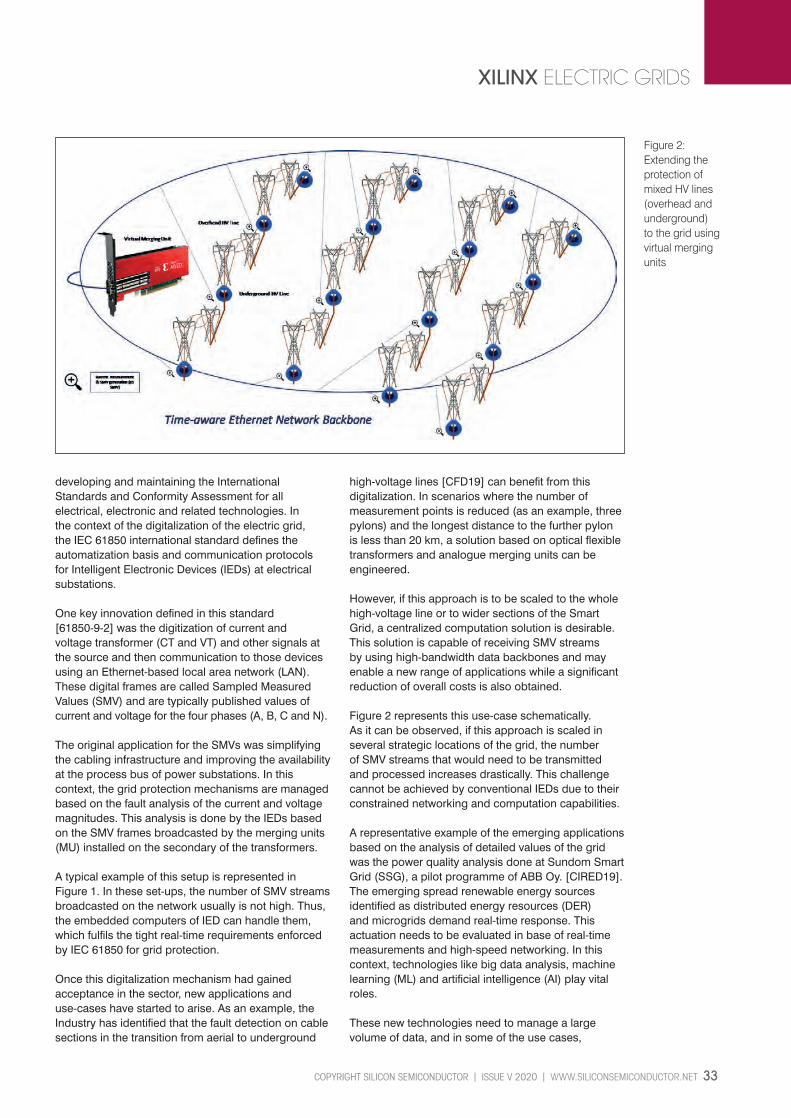
COPYRIGHT SILICON SEMICONDUCTOR l ISSUE V 2020 l WWW.SILICONSEMICONDUCTOR.NET 33
XILINX ELECTRIC GRIDS
developing and maintaining the International Standards and Conformity Assessment for all electrical, electronic and related technologies. In the context of the digitalization of the electric grid, the IEC 61850 international standard defines the automatization basis and communication protocols for Intelligent Electronic Devices (IEDs) at electrical substations.
One key innovation defined in this standard [61850-9-2] was the digitization of current and voltage transformer (CT and VT) and other signals at the source and then communication to those devices using an Ethernet-based local area network (LAN). These digital frames are called Sampled Measured Values (SMV) and are typically published values of current and voltage for the four phases (A, B, C and N).
The original application for the SMVs was simplifying the cabling infrastructure and improving the availability at the process bus of power substations. In this context, the grid protection mechanisms are managed based on the fault analysis of the current and voltage magnitudes. This analysis is done by the IEDs based on the SMV frames broadcasted by the merging units (MU) installed on the secondary of the transformers.
A typical example of this setup is represented in Figure 1. In these set-ups, the number of SMV streams broadcasted on the network usually is not high. Thus, the embedded computers of IED can handle them, which fulfils the tight real-time requirements enforced by IEC 61850 for grid protection.
Once this digitalization mechanism had gained acceptance in the sector, new applications and use-cases have started to arise. As an example, the Industry has identified that the fault detection on cable sections in the transition from aerial to underground
high-voltage lines [CFD19] can benefit from this digitalization. In scenarios where the number of measurement points is reduced (as an example, three pylons) and the longest distance to the further pylon is less than 20 km, a solution based on optical flexible transformers and analogue merging units can be engineered.
However, if this approach is to be scaled to the whole high-voltage line or to wider sections of the Smart Grid, a centralized computation solution is desirable. This solution is capable of receiving SMV streams by using high-bandwidth data backbones and may enable a new range of applications while a significant reduction of overall costs is also obtained.
Figure 2 represents this use-case schematically. As it can be observed, if this approach is scaled in several strategic locations of the grid, the number of SMV streams that would need to be transmitted and processed increases drastically. This challenge cannot be achieved by conventional IEDs due to their constrained networking and computation capabilities.
A representative example of the emerging applications based on the analysis of detailed values of the grid was the power quality analysis done at Sundom Smart Grid (SSG), a pilot programme of ABB Oy. [CIRED19]. The emerging spread renewable energy sources identified as distributed energy resources (DER) and microgrids demand real-time response. This actuation needs to be evaluated in base of real-time measurements and high-speed networking. In this context, technologies like big data analysis, machine learning (ML) and artificial intelligence (AI) play vital roles.
These new technologies need to manage a large volume of data, and in some of the use cases,
Figure 2: Extending the protection of mixed HV lines (overhead and underground) to the grid using virtual merging units
Xilinx v3.indd 33Xilinx v3.indd 33 02/12/2020 15:2802/12/2020 15:28

34 WWW.SILICONSEMICONDUCTOR.NET l ISSUE V 2020 l COPYRIGHT SILICON SEMICONDUCTOR
XILINX ELECTRIC GRIDS
with real-time requirements. The following analysis quantifies a potential real set-up: the maximum size of a SMV frame is 140 bytes, and a typical sampling rate is 4 Khz. Therefore, the required data bandwidth for each SMV is 448 Mbps.
According to the Wind Europe report 2019, the number of wind installations in Europe (on-shore and off-shore) is close to 190,000 [ENTSO19]. In a potential on-premises aggregation of information from 200 DERs in a small region, assuming 80 measurement points in each, the number of SMV that should be processed in real-time would be 16,000. In total, approximately 72 Gbps of net data would need processing under real-time conditions.
These magnitudes are far from the typical computing capacity of IEDs, which are usually capable of processing less than 10 SMV per unit. And is even for dedicated CPU processors like Intel Quad-Core i5 that saturates with 80 SMV [CIRED19]. Therefore, the need for a hardware acceleration would really help to enable this new generation of big data analysis applications.
Solution at Reconfigurable Silicon LevelAcceleration of computation using dedicated hardware is a hot topic. GPUs and FPGAs are massively used in the latest generations of edge and cloud equipment. The acceleration in applications that process very high numbers of SMVs requires high-speed data packet processing and digital signal processing (DSP). Specifically, the extraction and reordering of the payload is done at the packet
processing level. Typical DSP operations include the Discrete Fourier Transformation (DFT) to extract the harmonic composition; the root mean square (RMS) computation to know the effective values of current and voltage; phase calculation and custom decimation of the raw SMV stream for further computations.
This hardware processing requires flexibility. The format of the SMV frames varies depending on the standard and configuration that applies. Moreover, the computation that shall be accelerated by hardware may vary depending on the final goal. The new generation FPGAs and reconfigurable SoC offer this flexibility and allow a fully pipelined implementation in the logic of the packet processing followed by the custom DSP.
The product SMVsubscriber from SoC-e [SMVsubscriberIP] is running on Xilinx devices and therefore benefits from this approach. It allows the deterministic processing of massive SMV streams with very low latency. Each IP instance is able to process in parallel from 128 to 320 simultaneous SMV streams on the process Window configuration. The computation is deterministic in the range of 6 µs of latency for a full computation.
Each IP instance supports a standard stream on-chip bus, AXI-4 stream, which enables the interconnection with Ethernet switch IPs, like the 10G Managed Switch Ethernet IP. Internally, this switching IPs work as a SMV frame splitter to distribute the load among the parallel SMVsubscriber instances as it is depicted in Figure 3.
Figure 3:A SMV Subscriber Accelerator over Xilinx Alveo U50 card; compact and low-profile acceleration card models like the Alveo™ U50 from Xilinx specifically target on-premises acceleration.
Xilinx v3.indd 34Xilinx v3.indd 34 02/12/2020 15:2802/12/2020 15:28

COPYRIGHT SILICON SEMICONDUCTOR l ISSUE V 2020 l WWW.SILICONSEMICONDUCTOR.NET 35
XILINX ELECTRIC GRIDS
Acceleration al Platform Level: Xilinx Alveo Accelerator CardThe new generation of acceleration cards based on reconfigurable logic are boosting data driven workloads including high performance computing, networking, computational storage acceleration, data analytics and video processing, many of these are tied to Industrial IoT applications.
Recently, new compact and low-profile acceleration card models like the Alveo™ U50 from Xilinx specifically target on-premises acceleration. This combination is very attractive to implement aggregated and accelerated computations focused on industrial or energy applications. These sectors demand a practical trade-off between edge and cloud computing and typically rely on small data centres or isolated high-end industrial PCs on-premises.
Xilinx Alveo is the product line of accelerator cards with the variants: Alveo U200, Alveo U250, Alveo U280, as well as the new Alveo U50 referred to in this article. All cards of this product family are made for the acceleration cloud and edge (on-premises) applications. A key differentiator of the entire Alveo line-up is the existence of local data (Ethernet) interfaces in addition to the PCIe connectivity, which makes them ideal for networked applications like the one that has been described in our article.
Xilinx Alveo U50 is a high-performance accelerator with a smaller form factor than previous generations of Alveo boards. It is passively cooled with a max thermal design power (TDP) of 75W (typical 50W) and it has passive thermal design in a single slot (half height, half length) and is therefore significantly smaller than the other Alveo boards. It comes with a QSFP28 cage for 100 Gbit traffic over the local interface in addition
to the PCIe connectivity with up to 2x PCIe Gen4 x 8 lanes. 8GB HBM on board are accessible with a memory bandwidth of 316GB/s.
The specified application SMV processing benefits from the adaptability of the board function with programmable logic. This is true in particular as described below: Parallel processing: Dedicate SMV processor functions scale with multiple instantiations High bandwidth network interfaces: Data can be transmitted and received directly without the need to go through an external host processor. Customization for application-specific network protocols: For IEC 61850 HSR and PRP are high availability network protocols that benefit from programmable logic.
The existence of this card enables a more cost-efficient network architecture by collapsing compute functions into one place.
The SMVsubscriber IP can be implemented in these kind of accelerator cards. Additionally, these boards provide high-speed networking interfaces that would provide a comprehensive solution for these applications as shown in Figure 3. Each IP instance accommodates a net Ethernet throughput of 1 Gbps supporting 128 SMV streams using the maximum precision. For a regular on-site location with 10G networking capabilities, if a single 10G link were attached to the card, it would provide a workload for 10 IP instances running in parallel.
This combination gives support for the processing of 1.280 SMV streams. This quantity could be doubled if the second network interface of the card were used following the same approach. The networking capabilities of these acceleration cards goes beyond
Figure 4: High level application for analysis of SMV streams.
Xilinx v3.indd 35Xilinx v3.indd 35 02/12/2020 15:2802/12/2020 15:28

36 WWW.SILICONSEMICONDUCTOR.NET l ISSUE V 2020 l COPYRIGHT SILICON SEMICONDUCTOR
XILINX ELECTRIC GRIDS
References[ENTSO19] ENTSO-E, ENTSO-E Area Wind Europe report 2019 , https://www.entsoe.eu, 2019.[61850-9-2] IEC 61850-9-2:2011, Communication networks and systems for power utility automation - Part 9-2: Specific communication service mapping (SCSM) - Sampled values over ISO/IEC 8802-3. http://www.iec.ch/. INTERNATIONAL ELECTROTECHNICAL COMMISSION (IEC), 2011.[smu615] ABB, Substation Merging Unit SMU615, Product Guide. https://library.e.abb.com/. 2019[CFD2019] ARTECHE GROUP, SDO CFD. FAULT DETECTION ON CABLE SECTIONS IN MIXED HIGH VOLTAGE LINES, https://www.arteche.com. 2019[CIRED19] P. Hovila et al., ADVANCED UTILIZATION OF BIG DATA FOR REAL-TIME MONITORING AND DATA ANALYTICS IN SUNDOM SMART GRID, 25th International Conference on Electricity Distribution, 2019.[SMVsubscriberIP] SoC-e S.L., SMVsubscriber IP Core, https://www.xilinx.com/products/intellectual-property/1-12hrhrp.html, 2019.[TSN20] IEEE Time Sensitive Networking Task Group, IEEE 802.1 Standards. http://www.ieee802.org/1/pages/tsn.html. 2020.[HSRPRPSOCEIP] SoC-e S.L., HSR-PRP Switch IP Core, https://www.xilinx.com/products/intellectual-property/1-30q4iz.html, 2012.[TSNSOCEIP] SoC-e S.L., Multiport TSN Switch IP. http://soc-e.com/mtsn-multiport-tsnswitch-ip-core/. 2020.
10G, supporting 100G links. Therefore, the scalability of the solution is feasible by selecting card models with higher FPGA capabilities.
In order to benefit from accelerated computation in on-premises servers or in the Cloud, a high-speed networking backbone is required. Alveo U50 supports 10G and 100G Ethernet speeds. Currently, IT operators and infrastructure suppliers offer these options to the utilities. Therefore, the availability of this connectivity in the Smart Grid will limit or enable the proliferation of new applications based on the massive and real-time processing of the status of the Grid.
Thanks to the reconfigurability of the technology implemented on Xilinx Alveo, combined with the network capabilities of the card, it is feasible to support not only legacy networking but also high-availability and deterministic Ethernet. As an example, zero-delay recovery time protocols, Parallel Redundancy Protocol (PRP, IEC 62439-3-Clause 4) and high-availability seamless redundancy (HSR, IEC 62439-3-Clause 5) are used in modern digital power substations to communicate GOOSE and SMV values. Additionally, time-sensitive networking -TSN- [TSN20] – new generation Ethernet with support for real-time
traffic, is also considered in the sector. All these specific protocols are integral on Alveo FPGA via IPs [HSRPRPSOCEIP, TSNSOCEIP].
With a single acceleration card, 16 smart-grid locations, e.g. DERs, could be served, assuming an estimation of 80 real-time measuring points for each premise done in the introduction. Figure 4 and Figure 5 (respectively) show a monitoring tool developed for SMV monitoring purposes and the Alveo setup running SMV subscriber accelerator application on a dedicated high-bandwidth PCIe expansion system in Bilbao (Spain).
The accelerator card model used in this setup is the Xilinx Alveo U50. It provides PCIe Gen4 to a host processor and also local Ethernet ports for 4x10 Gbit/s, 4x25 Gbit/s or 1x100 Gbit/s through QSFP28. 8 GB HBM is on board. It comes with a standard single slot PCIe card with a power consumption of 75 W maximum and passive cooling.
ConclusionThe digitization of the grid is a continuous process, both for operational and for user networks. Specifically, the Ethernet broadcasting of current and voltage values for control and protection applications is a reality on the newest digital power substations. New DER systems and power quality assessment applications demand technologies to process in real-time a large volume of these streams.
This article has presented an innovative solution to accelerate the computation of hundreds of SMV streams combining a silicon IP and a new generation FPGA based accelerator card. Specifically, SoC-e SMVsubscriber and 10G MES IPs have been implemented on a Xilinx U50 acceleration card in a pilot setup located in Bilbao (Spain).
This solution uncovers the complexity of the SMV processing and offers a high-level interface for the application designers.
Figure 5: SMV Subscriber Accelerator application over Alveo in a dedicated PCIe expansion chassis.
Xilinx v3.indd 36Xilinx v3.indd 36 02/12/2020 15:2802/12/2020 15:28

COPYRIGHT SILICON SEMICONDUCTOR l ISSUE V 2020 l WWW.SILICONSEMICONDUCTOR.NET 37
SONOSCAN IGBT MODULES
IGBT modules interrogated acousticallyIGBT failures, because of the typically high voltage and power levels, can be both costly and dangerous. It makes sense to find internal structural defects be-fore they have an opportunity to go wrong.
BY TOM ADAMS, CONSULTANT, NORDSON SONOSCAN
A GROUP of three small air voids is trapped in the solder that bonds an IGBT module to its heat sink. The voids happen to lie close enough to each other to prevent some of the heat from escaping cleanly from the area of the die just above them. Over time, the area above the voids may overheat and the die may fail electrically - and along with it the system it is part of.
IGBT failures, because of the typically high voltage and power levels, can be both costly and dangerous. It makes sense to find internal structural defects before they have an opportunity to go wrong.
X-ray and ultrasound can both perform the nondestructive imaging that is needed, but with some differences. The first is penetration. X-ray may not ade-quately penetrate the heat sink on some IGBT modules, to deliver its data. The X-ray beam reports local differences in attenuation, and the most frequent de-fects in IGBTs are air gaps and non-bonds. If the gaps are relatively thick, such as a void in solder, imaging may succeed, but if they are very thin, as in a non-bonded area, they may remain invisible because their impact on the beam’s at-tenuation is too slight.An Acoustic Micro Imaging tool such as a C-SAM® tool from Nordson SONOSCAN can readily penetrate the heat sink, but first it needs to solve an-other problem: the small water column that on other components couples the tool’s transducer to the top of the component cannot be used on the top surface of an unencapsulated IGBT module. Impure water coming in contact with the face of the module could invariably leave some residue from evaporation, and the IGBT’s voltage level is so high that the residue could become a con-ductive pathway, with disastrous consequences. IGBT modules area one the few comps types the only component type having this limitation.
For this reason an inverted acoustic micro imaging tool was developed in order to image IGBTs from below, through the heat sink. The transducer and its
wa-ter column both point upward at their station below the module, whose top surface remains dry. Because the bottom side of an IGBT module not covered by encapsulant, the modules can be imaged even after encapsulation.
As the tool’s transducer scans back and forth along the bottom surface of the heat sink, it carries out its pulse-echo function at individual x-y locations tens of thousands of times per second, and contributes one pixel for the acoustic image with each pulse. The sequence is this: the transducer launches a pulse upward into the column of water. the pulse strikes the water-to-heat sink interface, and is in part reflected back to the transducer and in part transmitted upward into the module. the reflected echo reports, among other things, the distance from the transducer to the surface of the heat sink at the bottom of the module the transmitted portion travels through the heat sink and reaches the interface between the heat sink and the solder
Figure 1. Monochrome acoustic image made by scanning through bottom of module shows defects in one die attach.
Sonoscan IGBT v2.indd 37Sonoscan IGBT v2.indd 37 02/12/2020 15:2702/12/2020 15:27

38 WWW.SILICONSEMICONDUCTOR.NET l ISSUE V 2020 l COPYRIGHT SILICON SEMICONDUCTOR
SONOSCAN IGBT MODULES
the heat sink-solder echo is reflected to the transducer, where it reports the distance and other data about the interface.
The process will continue upward through additional material interfaces until the pulse reaches the attachment of the die to the raft. But before it reaches the raft, it will report any unintended features it encounters in the solder. The unintended features consist almost entirely of air gaps, which may take the form of air bubbles in the solder or flat delaminations between two solid materials. This is when the three voids mentioned in the first paragraph would be imaged, and their distance from the heat sink surface recorded.
The air bubbles are actually the most imageable features in the module, because instead of presenting a solid-to-solid interface, they present a solid-to-gas (air) interface, which reflects more ultrasound (nearly 100%) back to the transducer than any other type of interface. Solid-to-solid interfaces tend to reflect 10 to 50 percent of the energy in an arriving pulse. No ultrasound penetrates the solid-to-air interface, so x-y locations lying directly beyond it will not be imaged.You can see these effects at work in the monochrome acoustic image in Figure 1. To make this image, ultrasound was pulsed upward through the heat sink, the solder, the raft, and the die attach material, and returned to the transducer by the same route.
The rounded white feature near the upper left is an air-filled void in the layer bonding this chip to the ceramic raft in the module. There is another large void near the lower left, and several smaller ones. This image was made by using a ‘gate.’ Since the pulse was launched three ma-terial layers below, to make the desired image the receiver needs to select only the echoes from the small slice of time during which echoes were reflected by this die.
At each x-y location, the transducer’s receiver waits after a pulse is launched until at precisely the right nanosecond after launch it is activated to accept whatever arrives from the gated depth - anything from no echo to, as here, the strongest possible echo. Probably thousands of ‘strongest possible’ echoes arrived at the receiver to make the x-y shape of this void appear white. Weaker echoes produce gray. No echo at all yields black.
There seem to be a few cracks in this die, visible as dark lines; one reaches the void at upper left. The indistinct black features mostly on the right half of the die are voids in the solder layer, which is closer to the transducer. They are above the gate set for the die that is being imaged. They are black because they are shadows from voids above the gate.
Being voids, and filled with air, they sent back their own echoes when the pulses coming from the transducer struck them, but their own echoes arrived at the transducer too early to be within the collecting gate and were ignored. But by preventing pulses from reaching the die, they sent their own acoustic shad-ows to the transducer. One might also explain the same phenomenon by saying that during the brief moment when the transducer was receiving echoes from the die attach, the areas beyond these voids had nothing too contribute.
Figure 2 is the acoustic image of the raft surface on one of the die on a IGBT. The colors here are reporting the vertical distance of the solder-filled space between the raft and heat sink surfaces. This figure extends vertically through the whole thickness of the solder. The raft is deepest in small areas at left center (pale green in color map at left) and highest at upper right (pale blue in color map), where there is so little solder that the raft surface probably comes close to touching the heat sink. The key features here are the non-uniform thickness of the solder and the numerous heat-blocking voids, some of which are quite large.
Collectively they may be capable of causing a region of the die just above to overheat and fail. Those voids that are light blue are likely in contact with the heat sink. But note that part of the upper right corner is the same color, because the solder in this region is very thin.
The large blue C-shaped void near the center lies above an-other large void that lies in the red-yellow depth. Non-uniform solder layers may lead to uneven heat dissipation and therefore unwanted stress. Non-uniform solder layers may lead to uneven heat dissipation and thus unwanted stress.Neither of the IGBT modules shown here would be candidates for incorporation into a product: they are simply too filled with anomalies. But in these high-power modules even a single small anomaly could lead to failure if the modules are being used close to their design specifications.
Figure 2. Light blue features are closest to heat sink, pale green are farthest above.
Sonoscan IGBT v2.indd 38Sonoscan IGBT v2.indd 38 02/12/2020 15:2702/12/2020 15:27

COPYRIGHT SILICON SEMICONDUCTOR l ISSUE V 2020 l WWW.SILICONSEMICONDUCTOR.NET 39
green pages directory
To promote your products and services contact: Shehzad Munshi T: +44 (0)1923 690 215E: [email protected]
Flow Solutions
Gas Delivery Systems
Your world of discovery,powered by our delivery.
www.appliedenergysystems.com
Ultra high purity gasdelivery solutions
for rigorous purity andprecision needs.
Gas Purifi ers
SO MUCHMORE THAN ACOMPONENT.
www.appliedenergysystems.com/pure
Advanced point-of-use,micro-bulk and bulk
gas purifier solutions
Flow Measurement
NON-CONTACT LIQUID
ON RIGID PLASTIC
FLOW MEASUREMENT
TUBES & PIPES
SONOTEC GmbH | [email protected] | www.sonotec.eu
Anzeige_Directory_SiS_36mmx72mm_2020-09-14.indd 115.09.2020 10:25:10
Wet Process
SUPERIORWET PROCESSINGEQUIPMENT
Solder Rework
(610) [email protected]
WWW.SEMI-GAS.COM
Ultra-High Purity Gas Source, Distribution, and Control Systems
(610) [email protected]
WWW.SEMI-GAS.COM
Plasma Technology
Hydrogen Generators
MFCsEtch
Clean Rooms
Vacuum Equipment
SiS Corporate Partners Issue 5 2020 v1.indd 39SiS Corporate Partners Issue 5 2020 v1.indd 39 02/12/2020 15:2402/12/2020 15:24

Untitled-12 1Untitled-12 1 19/10/2020 10:1519/10/2020 10:15