
Handbook of Silicon Semiconductor Metrology · 2015-07-28 · 2 Handbook of Silicon Semiconductor...
57
1 Handbook of Silicon Semiconductor Metrology TABLE OF CONTENTS 1. Metrology Data Management and Information Systems ........................................................ 2 1.1. Introduction to Semiconductor Yield Management ............................................................ 2 1.1.1. Yield Learning ........................................................................................................... 3 1.1.2. The Defect Reduction Cycle ...................................................................................... 5 1.1.3. Yield Management Tools and Systems ...................................................................... 7 1.2. Data Sources ..................................................................................................................... 13 1.2.1. Defect Metrology ..................................................................................................... 13 1.2.2. Laboratory Defect Analysis ..................................................................................... 14 1.2.3. Process Metrology.................................................................................................... 15 1.2.4. Parametric Electrical Testing ................................................................................... 15 1.2.5. Sort Testing .............................................................................................................. 16 1.2.6. WIP Data .................................................................................................................. 17 1.2.7. Industry Formats for Data Transmission and Storage.............................................. 18 1.3. Analysis and Information ................................................................................................. 19 1.3.1. Yield Prediction ....................................................................................................... 20 1.3.2. Automatic Defect Classification .............................................................................. 23 1.3.3. Spatial Signature Analysis ....................................................................................... 25 1.3.4. Wafer Tracking ........................................................................................................ 30 1.4. Integrated Yield Management .......................................................................................... 32 1.4.1. Rapid Yield Learning through Resource Integration ............................................... 33 1.4.2. The Virtual Database ............................................................................................... 35 1.4.3. Data Mining and Knowledge Discovery.................................................................. 36 1.5. Conclusion ........................................................................................................................ 37 1.6. References ........................................................................................................................ 38 1.7. Figure Captions................................................................................................................. 45
Transcript of Handbook of Silicon Semiconductor Metrology · 2015-07-28 · 2 Handbook of Silicon Semiconductor...
1
Handbook of Silicon Semiconductor Metrology
TABLE OF CONTENTS
1. Metrology Data Management and Information Systems ........................................................ 21.1. Introduction to Semiconductor Yield Management............................................................ 2
1.1.1. Yield Learning ........................................................................................................... 31.1.2. The Defect Reduction Cycle ...................................................................................... 51.1.3. Yield Management Tools and Systems...................................................................... 7
1.2. Data Sources ..................................................................................................................... 131.2.1. Defect Metrology ..................................................................................................... 131.2.2. Laboratory Defect Analysis ..................................................................................... 141.2.3. Process Metrology.................................................................................................... 151.2.4. Parametric Electrical Testing ................................................................................... 151.2.5. Sort Testing.............................................................................................................. 161.2.6. WIP Data.................................................................................................................. 171.2.7. Industry Formats for Data Transmission and Storage.............................................. 18
1.3. Analysis and Information ................................................................................................. 191.3.1. Yield Prediction ....................................................................................................... 201.3.2. Automatic Defect Classification .............................................................................. 231.3.3. Spatial Signature Analysis ....................................................................................... 251.3.4. Wafer Tracking ........................................................................................................ 30
1.4. Integrated Yield Management .......................................................................................... 321.4.1. Rapid Yield Learning through Resource Integration ............................................... 331.4.2. The Virtual Database ............................................................................................... 351.4.3. Data Mining and Knowledge Discovery.................................................................. 36
1.5. Conclusion ........................................................................................................................ 371.6. References ........................................................................................................................ 381.7. Figure Captions................................................................................................................. 45
2
Handbook of Silicon Semiconductor Metrology
Volume EditorAlain C. Diebold
SEMATECH, 2706 Montopolis Drive, Austin, TX 78741
1. Metrology Data Management and Information Systems
AuthorsKenneth W. Tobin
Oak Ridge National Laboratory, P.O. Box 2008, Bldg. 3546, MS-6011, Oak Ridge,Tennessee 37831-6011
Ph: (865) 574-8521, Fax: (865) 574-6663, E-mail: [email protected]
Leonard Neiberg
Intel Corp., 5200 N.E. Elam Young Parkway, Hillsboro, Oregon 97124-6497
Ph: (503) 613-8005, Fax: (503) 613-6494, E-mail: [email protected]
1.1. Introduction to Semiconductor Yield Management
Semiconductor device yield can be defined as the ratio of functioning chips shipped
versus the total number of chips manufactured. Yield management can be defined as the
management and analysis of data and information from semiconductor process and
inspection equipment for the purpose of rapid yield learning coupled with the
identification and isolation of the sources of yield loss. The worldwide semiconductor
market will experience chip sales of $144 billion in 1999 increasing to $234 billion by
2002 [1]. Small improvements in semiconductor device yield of tenths of a percent can
save the industry hundreds of millions of dollars annually in lost products, product re-
work, energy consumption, and the reduction of waste streams.
3
Semiconductor manufacturers invest billions of dollars in process equipment, and they
are interested in obtaining as rapid a return on their investment as can be achieved. Rapid
yield learning is thus becoming an increasingly important source of competitive
advantage. The sooner an integrated circuit device yields, the sooner the manufacturer
can generate a revenue stream. Conversely, rapid identification of the source of yield
loss can restore a revenue stream and prevent the destruction of material in process [2].
The purpose of this section is to introduce the concepts of yield learning, the defect
reduction cycle, and yield management tools and systems as they relate to rapid yield
learning and the association of defects (referred to as “sourcing”) to tools and processes.
Overall, it is the goal of this article to present and tie together the different components of
integrated yield management (IYM) beginning with the very basic measurement and
collection of process data at the source in Section 1.2, Data Sources. Section 1.3,
Analysis and Information, describes the extraction of additional process information (i.e.,
what might be called meta-data) from the source data for the purpose of reducing the data
to smaller, informational-bearing quantities. These analysis techniques and strategies
represent relatively new research and development that address the issue of increasing
data volumes in the manufacturing process. Finally, Section 1.4, Integrated Yield
Management, describes the integration of the various sources of data and information for
the purpose of yield learning and prediction.
1.1.1. Yield Learning
Yield management is applied across different phases of the yield learning cycle. These
phases are represented in the top portion of Fig. 1 beginning with exploratory research
4
and development (R&D) and process development, followed by a yield learning phase
during the yield ramp, and finally yield monitoring of the mature manufacturing process.
The nature and quantity of data available to the manufacturer varies greatly depending on
the development stage of the process. In the first stage of exploratory research, relatively
small quantities of measurements are made due to the very low volume required to
support feasibility studies and experiments. As manufacturability matures from the
process development stage to the yield learning stage, automated data collection and test
routines are designed and put into place to maximize yield learning while maintaining or
increasing wafer throughput [3]. At these stages of manufacturing the number of device
measurements reaches its maximum, possibly several thousand per chip [3], and
encompasses both random and systematic defect sources.
For the purposes of this discussion, random defects are defined as particles that are
deposited on the wafer during manufacturing that come from contamination in process
gases, tool chambers, wafer handling equipment, and airborne particulates in the
fabrication environment. Random particles are characterized statistically in terms of
expected defect densities, and are the limiting source in the theoretical yield that can be
achieved for an integrated circuit device. Systematic defects are associated with discrete
events in the manufacturing process; such as scratches from wafer handling equipment,
contamination deposited in a non-random pattern during a deposition process, micro-
scratches resulting from planarization processes, or excessive pattern etch near the edge
of a wafer. Figure 2 shows examples of a random particle distribution in (a) versus a
systematic distribution in (b). During yield learning, random and systematic yield loss
both occur to various extents with systematic yield loss dominant early-on and random
5
defect yield loss dominant later. As manufacturing approaches the yield monitoring
phase of mature production, systematic yield loss becomes more rare and random defects
become the dominant and limiting source of yield loss in the process.
The amount of experimental design versus baseline analysis varies across the yield
learning cycle as well. This is represented in the bottom portion of Fig. 1.
Experimentation refers to the process design sequence and the design of appropriate tool
parameters (i.e., recipes) required to achieve a desired product specification, e.g., line
width, film thickness, dopant concentration, etc. Experiments are performed by varying
many operational parameters to determine an optimal recipe for a process or tool.
Baseline analysis refers to the establishment of an average expectation for a process or
tool. The baseline operating parameters will produce an average wafer of a given yield.
As yield learning is achieved, the baseline yield will be upgraded to accommodate
lessons-learned through process and equipment recipe modifications. As the process
matures for a given product, process and tool experiments are replaced by baseline
analysis until a stable and mature yield is achieved.
1.1.2. The Defect Reduction Cycle
It has been estimated that up to 80% of yield loss in the mature production of high
volume integrated circuits can be attributed to visually detectable random, process-
induced defects (PIDs) such as particulates in process equipment [4, 5]. Yield learning in
the semiconductor manufacturing environment can therefore be closely associated with
the process of defect reduction. Figure 3 shows the process by which yield learning is
approached by many semiconductor manufacturers today [6].
6
At the top of the cycle is the yield model that is used to predict the effects of process
induced defectivity on the function and yield of devices. The model is used to predict
process yield and to allocate defect budgets to semiconductor process equipment [7].
Defect detection encompasses a group of critical inspection methods for evaluating and
estimating the efficacy of manufacturing on devices that can not be tested for electrical
function at early production stages. Inspection can be broken into two major categories,
in-line and off-line. In-line inspection takes place in the fab and typically depends on
optical microscopy and laser scattering systems to scan large areas of the wafer. The
result of in-line inspection is a wafermap file containing information about the defect
location and size along with process information such as layer, lot number, slot position,
etc. The wafermap information is stored in the data management system (DMS) and
contains an electronic roadmap of defect sites that are used to relocate defects for detailed
analysis during off-line review. Off-line review is a materials characterization and failure
analysis process and methodology that includes many inspection modalities such as high-
resolution color optical microscopy, confocal optical microscopy, scanning electron
microscopy (SEM), atomic force microscopy (AFM), and focussed ion beam (FIB) cross
section analysis. In-line review is typically non-destructive and relatively timely (i.e,
keeps up with the manufacturing process through the application of computer vision)
whereas off-line techniques are typically destructive (e.g., SEM or FIB) and are
expensive, tedious, and time-consuming.
The main purpose for collecting defect, parametric, and functional test data is to facilitate
the sourcing and discovery of defect creation mechanisms, i.e., isolating the tools and
processes that are damaging the wafer and investigating and correcting these errant
7
conditions as rapidly as possible. Much of the day-to-day yield management activities
are related to this process. Defect sourcing and mechanism identification represents a
tactical approach to addressing yield loss issues. The learning that takes place in
conjunction with this day-to-day process is used to develop a strategic approach to defect
prevention and elimination, i.e., reducing the likelihood of yield loss from reoccurring in
the future by the modification or redesign of processes and products. Finally, the
reduction and elimination of the various sources of defects and parametric yield loss
mechanisms is fed back into the yield model, effectively closing the defect reduction
cycle.
1.1.3. Yield Management Tools and Systems
The variety, extent, and rate of change of both manufacturer-developed and commercially
available yield management systems in the field today precludes an exhaustive
description of these capabilities. The types of data that are measured and maintained in
the yield management database are also varied but include a common subset that we will
refer to throughout this discussion. These data and definitions are:
• Defect Metrology - Defect data collected from in-line inspection and off-
line review microscopy and laser scattering equipment. These data are
typically generated across a whole wafer, and an electronic wafermap, i.e.,
digital record, is generated that maintains information on the location and size
of detected defects. There may also be defect classification information in
this record supplied through manual engineer classification or automatic

8
defect classification systems during off-line review or in-line on-the-fly defect
classification.
• Equipment Metrology - This includes measurements that represent physical
characteristics of the device or wafer such as line width, location of
intentionally created fiducial features, film thickness, and overlay metrology.
Imagery can also be created by metrology inspection as described below.
• Imagery - Images collected from off-line review tools corresponding to
defects detected in-line are also maintained in the yield management database.
These images come from many different imaging modalities such as optical
microscopy, confocal microscopy, SEM, AFM, and FIB cross-section
microscopy. Included in this category of data can be images that represent
physical characteristics of the wafer such as critical dimension and overlay
metrology. The later two categories are not related to defect and pattern
anomalies, but rather to geometric characteristics of the patterns and layers.
• Parametric / Binmap and Sort - This category of data is commonly
referred to as electrical test data. Electrical testing is performed to verify
operational parameters such as input and output voltage, capacitance,
frequency, and current specifications. The result of parametric testing is the
measurement and recording of a real-valued number, whereas a bin or sort test
results in the assignment of a pass/fail code for each parametric test
designated as a bin code. The bin codes are organized into a whole-wafer
record called a binmap, analogous to the wafermap described above. The
binmap is used to characterize the manufacturing process in terms of
9
functional statistics, but it is also used to determine which devices will be
sorted for pass or fail, i.e., which devices yield and will be sold. For this
reason, binmap data is also referred to as sort data and is a fundamental
measurement of yield. It should be noted that die sort based on chip
processing speed is critical since current in-line critical dimension and dopant
control does not ensure that in-line binning is the same as final sort.
Parametric testing in the form of electrical testing is also used to infer other
non-electrical parameters such as line width and film thickness.
• Bitmap - Electrical testing of memory arrays to determine the location of
failed memory bits resulting in a whole-wafer data record analogous to the
wafermap described above.
• In-situ sensors - These are tool-based sensors that measure a given
characteristic of a process such as particle counts, moisture content, or end-
point detection in an etch process. In-situ sensors can be advantageous in that
they measure properties of the process, potentially before a drifting tool
causes significant yield impact to the product. In-situ sensor data is inherently
different in its structure and form since it does not spatially describe product
quality like visual or electrical inspection. In-situ data is time-based and
describes the state of the process over a period of time. An in-situ
measurement may encompass a single wafer process or a wafer lot process.
• Tool condition / tool health - Every process tool generates a monitor signal
used for local tool control; e.g., temperature, pressure, gas flow rate, or radio
frequency power level. This data is increasingly being maintained for use in
10
prognostics, diagnostics, preventive maintenance, and health assessment of
the process tools and equipment. As with in-situ sensors, tool health data is
time-based and describes the state of the process over a period of time.
• Work-in-process (WIP) - This corresponds to the wafer tracking system.
This data describes the processes, tooling, and recipes required to manufacture
a desired product. It is also used to track wafers and lots while in process. It
represents the initial planning for processing wafers in the plant and it
contains a wafer history of which tools and processes the wafer was exposed
to during production. This data is key to associating yield loss with specific
processes and equipment, i.e., tool isolation.
• Computer-aided design (CAD) - CAD data contains the electronic layout
for the integrated circuit. Layout is a complicated process by which a
composite picture, or record, of the circuit is generated layer-by-layer and
supplied to the manufacturer to create lithography masks and WIP
information. It should be noted that the design data represented by the
electronic CAD drawing is not typically integrated into the yield management
environment but holds much promise for providing feedback and design
modification to optimize the layout to mitigate the effects of random and
systematic defectivity impact on the device.
More detailed descriptions of the nature of these and related data sources are provided in
Section 1.2, Data Sources. A typical yield management database contains various
proportions of the data types described above and these data are maintained within the
database for various lengths of time. Table 1 shows the average distribution of these data
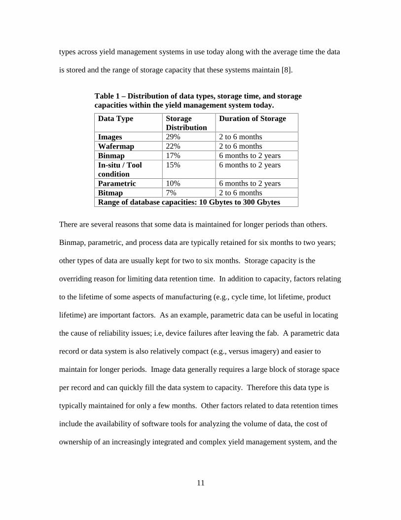
11
types across yield management systems in use today along with the average time the data
is stored and the range of storage capacity that these systems maintain [8].
There are several reasons that some data is maintained for longer periods than others.
Binmap, parametric, and process data are typically retained for six months to two years;
other types of data are usually kept for two to six months. Storage capacity is the
overriding reason for limiting data retention time. In addition to capacity, factors relating
to the lifetime of some aspects of manufacturing (e.g., cycle time, lot lifetime, product
lifetime) are important factors. As an example, parametric data can be useful in locating
the cause of reliability issues; i.e, device failures after leaving the fab. A parametric data
record or data system is also relatively compact (e.g., versus imagery) and easier to
maintain for longer periods. Image data generally requires a large block of storage space
per record and can quickly fill the data system to capacity. Therefore this data type is
typically maintained for only a few months. Other factors related to data retention times
include the availability of software tools for analyzing the volume of data, the cost of
ownership of an increasingly integrated and complex yield management system, and the
Table 1 – Distribution of data types, storage time, and storagecapacities within the yield management system today.
Data Type StorageDistribution
Duration of Storage
Images 29% 2 to 6 monthsWafermap 22% 2 to 6 monthsBinmap 17% 6 months to 2 yearsIn-situ / Toolcondition
15% 6 months to 2 years
Parametric 10% 6 months to 2 yearsBitmap 7% 2 to 6 monthsRange of database capacities: 10 Gbytes to 300 Gbytes
12
lack of standards for acquiring and storing information such that it can be efficiently
retrieved and used at a later date.
Figures 4 and 5 represent a simplified description of two extremes in current yield
management architectures and philosophies across a broad category of semiconductor
manufacturers [8]. In Fig. 4 each independent database is represented according to the
data type maintained. The shaded regions represent areas where commercial yield
management systems are finding the highest acceptance to date. Other non-shaded
regions represent technologies that tend to be designed and implemented in-house by the
yield engineering team.
Figure 5 represents the highest level of database integration observed to date [8]. This
configuration is not as common due to the requirement that data from legacy database
systems need to be replaced with newer technologies to achieve high levels of
integration. To implement a configuration such as that shown in the figure requires that
older databases and systems be ported to newer technology platforms. Therefore, the
general trend in yield management systems technology is to move towards distributed
systems while attempting to integrate more of the data from these systems for
engineering (i.e., investigative) analysis. Facilities to measure, store, and maintain in-situ
process data and tool condition data are the least mature while the ability to measure,
store, and maintain wafer-based data (e.g., defect, parametric, binmap, and bitmap) are
the most advanced. The primary issue with in-situ and tool health data is that it is time-
based, not wafer-based. Correlating time-based data with wafer-based data for yield
analysis is difficult to implement.
13
Although yield management systems and capabilities are continuing to mature at a rapid
pace, there are many areas of standards, infrastructure, and technology that are continuing
to be addressed in an evolutionary sense. Figure 6 represents a roadmap of several of the
most pressing issues that are being addressed by yield engineers, information technology
teams, and standards organizations today regarding the evolution of semiconductor DMS.
1.2. Data Sources
This section will describe in more detail many of the data sources initially listed in
Section 1.1.3, Yield Management Tools and Systems, and will enable a discussion of the
uses of this data for analysis in Section 1.4, Integrated Yield Management. The character
of semiconductor manufacturing is noteworthy for the number and variety of data sources
that can be collected and used for yield and product performance enhancement. Aside
from WIP data and final test data, which are collected as a by-product of the fabrication
process, many data sources are explicitly created at substantial expense as an investment
in accelerating yield learning. The primary examples of additional data sources in this
category are defect metrology, equipment metrology, laboratory defect analysis, and
parametric electrical test.
1.2.1. Defect Metrology
Defect metrology data can be described as the identification and cataloging of physical
anomalies seven on the wafer at intermediate operations during manufacturing.
Individual detectable defects are not guaranteed to cause functional failures (e.g., an
organic particle that is later removed during an etch operation), nor are all defects that
cause failures guaranteed to be detected by defect metrology equipment during
14
manufacturing (e.g., non-functional transistors caused by inadequate ion implantation).
The key challenge in optimizing a defect metrology scheme is to maximize the detection
of the defects which are likely to cause functional failures (commonly called “killer
defects”) while minimizing the resources which detect non-killer (or “nuisance”) defects.
Due to this objective and the complexities of defect metrology equipment, defect
metrology data collection has historically been divided into two phases: inspection and
review. Inspection is the automated identification and collection of data such as defect
size, imagery, and automatic categorization, while defect review is typically a time-
intensive, manual process where additional data and imagery are collected for targeted
defects of interest identified during the inspection process. Although this data is critical
for yield learning, it is expensive to collect. In practice, only a fraction of the total
number of wafers in a fab are inspected; and of those inspected only a smaller fraction are
reviewed.
1.2.2. Laboratory Defect Analysis
Once wafer fabrication has been completed or once a specific device structure has been
covered by another layer (e.g., transistor gates that are physically covered by the first
metallization layer), further analysis of defects is possible only with significant difficulty.
The main complication is the requirement to remove the covering material to expose the
defects of interest. Once the desired material is removed through a variety of resource-
intensive processes, the target area can be analyzed with laboratory equipment. This
equipment is capable of taking extremely high-resolution imagery (e.g., on the order of
10 nm – 100 nm) in conjunction with material composition analysis though the use of
techniques including focused ion beam etching, SEM, and energy dispersive x-ray

15
spectroscopy (EDX). These techniques allow the collection of even more detailed data
than is available from other types of metrology for the purpose of identifying the root
cause of a particular defect.
1.2.3. Process Metrology
Different types of data collection tools are used to determine if the width, thickness, and
physical placement of intentionally created features meets specification limits. The most
common examples of such metrology are critical dimension (CD) measurement of lines,
trenches, and vias, thin films metrology (i.e., measurement of the thickness of deposited,
etched, or polished film layers), and registration (i.e., measurement of the relative
alignment between two layers of structures, e.g., between a via at metal level two and the
corresponding landing pad at metal level one). Such metrology can be used to
characterize critical non-defect related contributors to yield loss (e.g., overly thick
transistor gates which lead to unacceptable device performance).
1.2.4. Parametric Electrical Testing
The ability to measure the electrical behavior of the silicon is invaluable in yield analysis.
The collection of such data relies on the intentional creation of electrical test structures.
In the layout process, simple circuits are created that enable the measurement of
parametric (i.e., non-categorical real valued) quantities such as sheet resistance,
transistor-off current, etc. The collection of the data from these structures is performed
by electrical test equipment which places electrical probes on special contact pads,
creates specific test inputs on several probes, and reads the electrical conditions present at
other probes. Probe outputs can then be input to analysis equations based on the test
16
circuit design to determine the value of the desired parametric value. There can be
several hundred different parametric electrical tests that are collected at several sites
across a wafer, such as capacitance or current. These values can be used to identify
wafer-to-wafer or across-wafer variability of critical electrical properties, as well as links
between physical properties of the silicon and functional device behavior.
1.2.5. Sort Testing
Sort testing is the final assessment of whether a specific die performs as desired and
should be targeted for assembly as a packaged part for sale. Sort test equipment makes
electrical contact with the output pads of the die, applies specific input patterns to some
pads, reads the outputs off other pads, and determines from these outputs whether the
circuitry performs the desired functions at the desired clock speed. There are three types
of sort data that can be obtained based on three different methodologies: bitmap testing,
functional testing, and structural testing. All sort testing applies input electrical patterns
to a set of electrical contacts and reads outputs from a set of output contacts, but the test
methodology dictates the character of data obtained.
Bitmap testing is only possible on memory circuitry such as SRAM, DRAM, or memory
cache. This testing performs read and write operations on each memory cell to determine
precisely which memory cells or groups of cells are functional and which are flawed.
Not only do these data provide detailed information regarding which devices are
functional enough for sale, but the data can also pinpoint the locations of the electrical
faults to enable laboratory failure analysis.

17
In contrast, functional testing subjects the die to a set of test input patterns which are
designed to exercise the main functions of the circuitry. Based on the specific failures
(i.e., actual output patterns which do not match target output patterns), each die is
classified as being a member of a particular “sort bin” which defines a general category
of functional behavior. For example, die categorized in bin one may be fully functional
at the desired clock speed, bin two may be for fully functional die at a less profitable
clock speed, bin three for die with an unacceptable number of cache failures, etc.
Depending on how the bins are defined, categorization of die in certain bins may indicate
the functional block of the die which is non-functional (e.g., arithmetic logic unit failure),
but such electrical fault localization is typically not at sufficient resolution to pinpoint the
exact location of the failure.
Structural test is a methodology that is designed to enable reliable localization of
electrical faults, even in random circuitry (i.e., it is not limited to memory circuitry) while
requiring less expensive test equipment than is required or functional testing. Ideally,
structural testing data will include not only sort bin data, indicating which functions are
inoperable, but also a list of electrical nodes or specific circuit structures that are faulty.
This fault localization can be used for laboratory failure analysis of random logic circuits.
The ability to accurately localize fault locations is a critical capability on the International
Technology Roadmap for Semiconductors [9], and structural testing is expected to play
an increasingly significant role in meeting that challenge.
1.2.6. WIP Data
WIP data is a general term that describes the processing chronology or history of a wafer.
This data consists of a list of all manufacturing operations to which a wafer was
18
subjected, and the specifics of the processing configuration at each operation. These
specifics include the time at which the processing occurred, the relative positions of each
wafer in the processing tool (e.g., slot position or processing order), the exact tool
settings or recipe used, etc.
The source of this data is the factory automation system; whose primary function is to
ensure that each wafer is processed exactly as specified. The unique process
specification is combinatorially complex given the hundreds of individual processing
operation, the tens of processing tools which can be used to execute each operation, and
the hundreds of configurations specified at each operation. Although the primary
function of the automation system is to ensure correct processing, the storage of WIP data
is required to identify a specific piece of process equipment as the root cause of yield
loss.
1.2.7. Industry Formats for Data Transmission and Storage
Although data collection methodologies and basic informational content for the above
data types are largely common across the industry, data file formats are not. In practice,
data file formats are specific to each tool that generates the data. As an example, there
are completely different defect metrology data formats for each of the separate tool types
sold by a single tool vendor. This multiplicity of data formats is one of the major factors
complicating yield analysis. This issue was discussed above in Section 1.1.3, Yield
Management Tools and Systems and represented as a main issue in Fig. 6 under
“Continuous Standards Activities”.
19
There are two mechanisms for the establishment of industry standards in the future.
Standards can emerge either by de facto adoption by tool suppliers or by official
establishment by a standards committee such as Semi or I300I. However, neither
mechanism for standards establishment is yet to have yielded significant results. The
impact of this lack of standardization will be described in Section 1.4, Integrated Yield
Management.
1.3. Analysis and Information
Semiconductor yield analysis makes use of multiple sources of data collected from the
manufacturing process; sources that are continuing to grow in volume due to increasing
wafer size and denser circuitry. This section begins with a review of the fundamental
techniques of statistical yield analysis. Yield is based on a measure of the fraction of
shippable product versus total input. This is typically determined at functional test when
each die on the wafer if electrically determined to pass or fail a set of operating
parameters. It is important to understand what is happening in the manufacturing process
prior to final test; therefore, there are a number of techniques for estimating instantaneous
device yield based on measurements of physical and parametric defects. Due to
increased wafer dimensions and decreasing line width, there are huge quantities of data
being collected in the fab environment. To accommodate this situation, there are new
levels of automation coming on line that result in the reduction of data for informational
purposes. Automatic defect classification (ADC), spatial signature analysis (SSA), and
wafer tracking techniques represent a few of these techniques that are described below in
relation to yield management, analysis, and prediction.
20
1.3.1. Yield Prediction
Yield can be defined as the fraction of total input transformed into shippable output.
Yield can be further subdivided into various categories such as [10],
• Line yield - the fraction of wafers not discarded prior to reaching final electrical
test,
• Die yield - the fraction of die on yielding wafers that are not discarded before
reaching final assembly and test, and
• Final test yield - the fraction of devices built with yielding die that are deemed
acceptable for shipment.
Yield modeling and analysis is designed as a means of proactive yield management
versus the traditional sometimes “reactive” approach that relies heavily on managing
yield crashes (i.e, “fire fighting”). A yield management philosophy that promotes the
detection, prevention, reduction, control, and elimination of sources of defects contributes
to fault reduction and yield improvement [11].
Semiconductor yield analysis encompasses developing an understanding of the
manufacturing process through modeling and prediction of device yield based on the
measurement of device function. Historically, the modeling of process yield has been
based on the fundamental (and simple) assumptions of binomial or Poisson statistics [12,
13], specifically that:
• the yield is binary, i.e., a device either functions or it does not function;

21
• the number of occurrences of failures are small relative to the population of
devices on the wafer;
• failure of a device on the wafer is uncorellated to the failure of any other device
on the wafer (or lot etc.), i.e., device failures are uncorellated and random; and
• yield is a simple function of active device area, A, and the average wafer defect
density, D, i.e., Y = e-AD, i.e. the Poisson distribution.
These assumptions typically hold true, to a reasonable approximation, for mature
processes where the yield is high and is limited primarily by random events. But during
the process development and yield learning stage, these models do not correlate well with
observed yields. To account for these inaccuracies, there have been some attempts to
incorporate defect clustering relationships and/or systematic defect processes into the
analysis models. It is at this point that the measurement of the spatial distributions of
defect/fault events begins to address correlated populations of defects as unique
systematic and repeatable signature events.
Yield modeling has application to yield prediction, i.e., an estimate of position on the
yield curve of Fig. 1, device architecture design, process design, and the specification of
allowable defectivity on new process tools necessary to achieve desired future yield
goals. In relation to process control, yield analysis has applicability to process
characterization, e.g., in relation to improving the rate of yield learning. To achieve this
last goal, it is important that yield modeling accommodate both systematic and random
defects. Once on top of the yield curve during the yield monitoring phase, systematic
mechanisms are a small portion of the overall defect source issue, but it should be noted
that manufacturing can remain in the yield learning phase for several years [15].

22
To accommodate systematic defect and fault distributions, researchers have modeled
concepts of defect “clustering” on wafermaps. The well known negative binomial yield
model [12] recognizes defect clustering by integrating the simple Poisson yield model
over an effective defect density distribution function f(D), i.e., Y = ∫ e-AD f(D) dD. This
result is the compound Poisson distribution model, well known as the negative binomial
relationship, Y = (1 + AD/α )-α, where α is defined as a clustering parameter which
accounts for the variability in defect densities from wafer-to-wafer or lot-to-lot. Different
values for α attempt to facilitate different models of clustering in the defect distributions
measured across a wafer and result in the relationships commonly used for yield
prediction that are shown in Table 2.
When clustering becomes very severe, i.e., the distributions of defects become more
dense and systematic, variations of these models shown in Table 2 are derived by
Table 2 – Yield models derived from the Poisson probability distribution.Each model accommodates a varying degree of clustering.
Degree of Clustering Yield Model
Poisson
No clustering, α > 7
ADeY −=
Murphy’s
Minor degree of clustering, α = 4.5( ) 21
−=−
AD
eY
AD
Negative Binomial
Moderate clustering, α = 2
α
α
−
−= AD
Y 1
Seed’s
Large degree of clustering, α = 1 ADY
+=
1
1
23
partitioning the wafer into discrete, independent zones, e.g., stepper fields, and/or
quadrant or radial zones [12, 14]. While this can improve the performance of the model,
partitioning methods are still susceptible to the limitations of the Poisson model, e.g., the
model assumes a random, uncorrelated distribution of defects in each zone, and a
generally small population of defects. An approach of this nature has been put forth by
SEMATECH for a 250 nm yield model [15] and a 150 nm yield model [16].
Simply detecting the onset of a systematic defect creation mechanism can be helpful to
catching a process that is drifting or moving rapidly out of control. Kaempf [17] has
shown how application of a simple binomial distribution model can be used to detect the
onset of systematic distributions, e.g., a reticle-induced defect (repetitive) pattern or an
edge ring pattern. A plot of yield probability as a function of device yield will deviate
from a binomial-shaped distribution as systematic events take precedence over random
ones. This technique, although simple to implement, requires a fairly large number of
data points, e.g., wafers and/or lots, before a determination can be made; and the method
can not resolve one type of systematic event from another, i.e., it is primarily an alarm for
process drift or excursion.
1.3.2. Automatic Defect Classification
ADC has been developed to provide automation of the tedious manual inspection
processes associated with defect detection and review. Although the human ability to
recognize patterns in data exceeds the capabilities of computers in general, effectively
designed ADC can provide a more reliable and consistent classification result than can
human classification under well-defined conditions. These conditions are typified by
highly manual and repetitive tasks that are fatiguing and prone to human error. Figure 7

24
shows representative examples of the variety of defect imagery that arise in
semiconductor manufacturing. These include examples of individual pattern and particle
defects sensed using optical and electron microscopy.
ADC was initially developed in the early ‘90s to automate the manual classification of
defects during off-line optical microscopy review [18, 19, 20]. Since this time, ADC
technologies have been extended to include optical in-line defect analysis [21] and SEM
off-line review. For in-line ADC, a defect may be classified “on-the-fly”, i.e., during the
initial wafer scan of the inspection tool, or during a re-visit of the defect after the initial
wafer scan. During in-line detection the defect is segmented from the image using a die-
to-die comparison or a “golden template” method as shown in Fig. 8 [22, 5]. This figure
shows an approach to defect detection based on a serpentine scan of the wafer using a
die-to-die comparison; first showing A compared to B, B compared to C, etc., ultimately
building a map of the entire wafer. During off-line review the defect is re-detected using
the specified electronic wafermap coordinates and die-to-die or golden template methods.
The classification decision derived from the ADC process is maintained in the electronic
wafermap for the wafer under test and will be used to assist in the rapid sourcing of yield
impacting events and for predicting device yield through correlation with binmap and
bitmap data if available.
Figure 9 shows an example of a frequency distribution of defects that can occur in a
manufacturing process. This particular data set came from a deep trench process and
shows the distribution of 18,840 classified defects across 314 wafers [23]. In the figure,
the defect classes are labeled as RE, SF, LI, HO, LS, etc., and the height of each bin is the
frequency of occurrence of each class. It is apparent from the data that 97% of the
25
defects that occurred in the deep trench process are of class LS (67%) and ST (30%). If
the cause of the defined defect categories is sufficiently characterized and maintained a-
priori in the yield management system, frequency distributions such as this are useful in
directing the engineer to the highest priority issues. In this case, the highest priority issue
may not be the most frequently occurring. In fact, it should be noted that not all detected
defects cause electrical failures. The ratio of defects that cause failures to the total
defects detected is termed the “kill ratio” [5]. A kill ratio can be determined for each
class of defect as well; therefore, giving a relative measure of importance to each
frequency bin shown in the figure. For example, if the kill ratio for category LS was 0.25
and the kill ratio for category ST was 0.9, then a prediction can be made that
(67%)×(0.25) = 17% of the total defect population are of the category killer-LS and
(30%)×(0.9) = 27% of the total population are killer-ST. Therefore, if the class-
dependent kill ratio is known, the ST category would be the more immediate yield
detracting mechanism to address. This type of statistical data also provides a
methodology to estimate device yield prior to electrical test.
1.3.3. Spatial Signature Analysis
It has been widely recognized that although knowledge of process yield is of primary
concern to semiconductor manufacturers, spatial information is necessary to distinguish
between systematic and random distributions of defects. Recall that Fig. 2 shows a
whole-wafer view of a random distribution of defects in (a) and a systematic pattern of
defects exhibiting both clustered events (e.g., scratches) and distributed systematic events
(e.g., a chemical vapor deposition contamination problem) in (b). Knowing that a
distribution has a spatial effect provides further information about the manufacturing

26
process, even if the distribution has little effect on device yield. Therefore, focusing only
on process yield, and ignoring the systematic and spatial organizations of defects and
faults represents a lost opportunity for learning more about the process [24].
When a high level of clustering is observed on wafermaps, simple linear regression
models can lead to inaccurate analysis of the yield data, such as negative yield
predictions. Ramirez, et al., discuss the use of logistic regression analysis with some
modifications to account for this negative yield prediction effect known as
“overdispersion” [25]. This technique attempts to accommodate clustering indirectly in
the model.
A more direct approach to handling defect clustering is demonstrated through the work of
Taam, et al. While defect clustering yield analysis has historically been treated by
application of the compound Poisson distribution model discussed in the previous section
(which imbeds the defect clustering in the yield model), Taam, et. al., uses a measure of
clustering based on the idea of nearest neighbors [24]. This method makes a direct
measure of the spatial relationships of good and bad die on a wafer. The method uses
join-count statistics and the log-odds ratio as a measure of spatial dependence. While the
technique does identify the occurrence of spatial events, wafermaps and join-count maps
(which reveal the joined clusters of die) are required to be analyzed manually to learn
more about the root cause.
Collica, et al., incorporate the methods of Ramirez [25] and Taam [24] using join-count
statistics and spatial log odds ratios to organize and describe spatial distributions of good
and bad die through the use of CUMSUM charts [26, 27]. The two main objectives of
the approach are to recognize and understand common causes of variation; which are
27
inherent in the process and identify special causes of variation that can be removed from
the process.
An interesting extension of this approach has been applied to the analysis of spatial bit
fail patterns in SRAM devices where Kohonen self-organizing maps and perceptron
back-propagation neural networks have been used to classify the spatial patterns. These
patterns occur, e.g., in vertical bit-line faults, horizontal single word faults, diagonal
doublets, clustered bit faults, etc. [28, 29].
The analysis of spatial patterns of defects across whole wafers is described above as a
means to facilitate yield prediction in the presence of systematic effects. Tobin, et al.,
have developed an automated whole-wafer wafer analysis technique called SSA to
address the need to intelligently group, or cluster, wafermap defects together into spatial
signatures that can be uniquely assigned to specific manufacturing processes and tools
[30, 31, 32, 33]. This method results in the rapid resolution of systematic problems by
assigning a label to a unique distribution; i.e., signature, of defects that encapsulate
historical experience with processes and equipment. Standard practice has been to apply
proximity clustering that results in a single event being represented as many unrelated
clusters. SSA performs data reduction by clustering defects together into extended
spatial groups and assigning a classification label to the group that reflects a possible
manufacturing source. Figures 10 and 11 show examples of clustered and distributed
defect distributions respectively that are isolated by the SSA technique. SSA technology
has also been extended to analyze electrical test binmap data (i.e., functional test and
sort) to recognize process-dependent patterns [34] in this data record.
SSA and ADC technologies are also being combined to facilitate intelligent wafermap
28
defect sub-sampling for efficient off-line review and improved ADC classifier
performance [23, 35, 36]. The integration of SSA with ADC technology can result in an
approach that improves yield through manufacturing process characterization. It is
anticipated that SSA can improve the throughput of an ADC system by reducing the
number of defects that must be automatically classified. For example, the large number
of defects that comprise a mechanical scratch signature that is completely characterized
by SSA will not need to be further analyzed by an ADC system. Even if a detected
signature cannot be completely characterized, intelligent signature-level defect sampling
techniques can dramatically reduce the number of defects that need to be sent to an ADC
system for subsequent manual or automated analysis (e.g., defect sourcing, tool isolation,
etc.).
The accuracy of an ADC system can potentially be improved by using the output of the
SSA wafermap analysis to perform focused ADC. Focused ADC is a strategy by which
the SSA results are used to reduce the number of possible classes that a subsequent ADC
system would have to consider for a given signature. SSA signature classification can be
used to eliminate many categories of potential defects if the category of signature can be
shown a-priori to consist of a limited number of defect types. This pre-filtering of
classes reduces the possible alternatives for the ADC system and, hence, improves the
chance that the ADC system will select the correct classification. It is anticipated that
this will result in improved overall ADC performance and throughput.
Another yield management area where SSA can provide value is in statistical process
control (SPC). Today, wafer-based SPC depends highly on the tracking of particle and
cluster statistics; primarily to monitor the contribution of random defects. Recall that
29
random defects define the theoretical limit to yield and controlling this population is a
key factor in achieving optimal fabrication performance. A cluster is defined as a group
of wafer defects that reside within a specified proximity of each other. Current strategies
typically involve removing cluster data from the population and tracking the remaining
particle data under the assumption that these are random, uncorrelated defects. Field
testing of the advanced clustering capabilities of SSA has revealed that this basic
approach can be modified dramatically to reveal much information regarding systematic
defect populations during the yield ramp.
For example, the last wafermap shown in row (a) of Fig. 10 contains a long, many-
segmented scratch that commonly used proximity clustering algorithms would categorize
as multiple clusters. The ability of SSA to isolate and analyze this event as one single
scratch removes ambiguity from the clustering result (i.e., the event is accurately
represented by a single group of defects, not many independent clusters). It allows the
user to assign process-specific information via the automatic classification procedure to
facilitate SPC tracking of these types of events to monitor total counts, frequency of
occurrence, etc. Care must also be taken in analyzing random events on a wafer. Row
(a) of Fig. 11 shows random populations of defects that are uncorrelated while rows (b)
and (c) show distributed (i.e., disconnected) populations that are systematic, i.e., non-
random, and can be related to a specific manufacturing process. If the pattern is
determined to be systematic, it is virtually impossible to separate random defects from the
distributed, systematic event. The current practice of filtering clusters based on
proximity alone would result in the counting of these systematic distributions as random
defects. Unless a yield engineer happens to view these maps, the count errors could go
30
undetected indefinitely resulting in the spurious rise and fall of random particle
population estimates. Using an approach such as SSA results in the separation of wafer
events into random and systematic events (i.e., both clustered and distributed) that
provide a higher level of information about the manufacturing process. Using this
informational content to separate and monitor random defects from systematic
distributions from scratches, streaks, and other clusters, provides the yield engineer a
much clearer window into the manufacturing process.
1.3.4. Wafer Tracking
A contemporary semiconductor process may consist of more than 500 intricate process
steps [5, 9]. A process drift in any of these discrete steps can result in the generation of
pattern or particle anomalies that effect other downstream processes and ultimately
reduce yield. Mechanisms for rapidly detecting and isolating the offending process step
and specific tools are required to perform rapid tool isolation. One such technique that is
becoming common place in the fab is wafer tracking. Wafer tracking involves
monitoring the location of each wafer in the process by reading the laser etched serial
number from the flat or notch of the wafer that is provided by the silicon manufacturer.
Tracking requires that an optical character recognition system and wafer sorter be located
at each critical step in the process. The serial number is then mapped to a precise
equipment location that is subsequently maintained by the DMS [37, 38]. This allows the
wafer to be followed down to the specific slot number or position in the carrier or process
tool. Using the silicon manufacturer’s serial number also allows the device manufacturer
to correlate process patterns with the suppliers silicon wafer parameters.
31
Yield and process engineers can refer to the wafer tracking information in the DMS to
resolve yield loss issues within the manufacturing line. For example, if an engineer
suspects a faulty furnace operation, a report can be generated from the DMS detailing the
deviating parameter (e.g., a parametric test result or yield fraction) for wafers versus their
location in the furnace tube. Wafer-level data also provides evidence of difficult process
problems when a hypothesis of root cause is not initially apparent. In the case of the tube
furnace, the engineer may generate a plot that shows the particular step or steps where the
impacted wafers were processed together. This discernment can be made because at each
wafer reading station the wafer positions are randomized by the automatic handler prior
to the subsequent processing step. The randomization takes place at every process step
and facilitates the isolation of particular tool and positional dependencies in the data.
This is typically viewed in a parameter-versus-position plot that will be ordered or
random, depending on the tool where the process impacted the lot. For example, a two-
dimensional plot with high yield on one end and low yield on the other would implicate a
specific tool versus a plot revealing a random yield mix that shows no correlation to that
tool.
Historically, wafer tracking has relied on the comparison of whole-wafer parameters such
as yield with positional information to determine correlations. A recent development in
wafer tracking incorporates spatial signature analysis to track the emergence of particular
signature categories and to correlate those events back to specific processes and tools
[39]. Recall that SSA maps optical defect clusters and electrical test failure wafermap
patterns to predefined patterns in a training library. Wafer tracking with SSA captures a
wafer’s position/sequence within various equipment throughout the fab, and correlates
32
observational and yield results to positional signatures. By frequently randomizing wafer
order during lot verification and processing, positional information provides a unique
signature of every process step. Integrating SSA with wafer tracking helps to resolve the
root causes of multiple yield loss mechanisms associated with defect and sort test
wafermap and positional patterns. This is accomplished by isolating individual defect
clusters (i.e., signatures) and identifying which process step most strongly correlates with
yield loss. It is anticipated that this capability will facilitate rapid yield learning,
particularly during the introduction of new processes.
1.4. Integrated Yield Management
As integrated circuit fabrication processes continue to increase in complexity, it has been
determined that data collection, retention, and retrieval rates increase geometrically. At
future technology nodes, the time necessary to source manufacturing problems must at
least remain constant, i.e., approximately 50% of the cycle time on average during yield
learning. In the face of this increased complexity, strategies and software methods for
integrated yield management (IYM) have been identified as critical for maintaining
productivity. IYM must comprehend integrated circuit design, visible defect, parametric,
and electrical test data to recognize process trends and excursions to facilitate the rapid
identification of yield detracting mechanisms. Once identified, the IYM system must
source the product issue back to a point of occurrence. The point of occurrence is
defined to be a process tool, design, test, or process integration issue that resulted in the
defect, parametric problem, or electrical fault. IYM will require a merging of the various
data sources that are maintained throughout the fabrication environment. This confluence
of data will be accomplished by both the physical and virtual merging of data from
33
currently independent databases. The availability of multiple data sources and the
evolution of automated analysis can provide a mechanism to convert basic defect,
parametric, and electrical test data into useful process information.
With the continued increase in complexity of the fabrication process, the ability to detect
and react to yield impacting trends and excursions in timely fashion will require a larger
dependence on passive data. This will be especially true during yield learning where
maximum productivity and profit benefits will be achieved. Passive data is defined as
defect, parametric, and electrical test data collected in-line from the product through
appropriate sampling strategies. The additional time required to perform experiments,
e.g., short-loop testing, will not be readily available at future nodes. The time necessary
to trend potential problems and/or identify process excursions will require the
development of sampling techniques that maximize the signal-to-noise ratio inherent in
the measured data. The goal of IYM is to identify process issues in as few samples as
possible. Analysis techniques that place product data in the context of the manufacturing
process provide a stronger “signal” and are less likely to be impacted by measurement
noise since they comprehend various levels of process history and human experience, i.e.,
lessons learned [9].
1.4.1. Rapid Yield Learning through Resource Integration
One of the few commonalities between virtually all semiconductor yield analysis is the
requirement to integrate multiple data sources. One of the simplest cases to illustrate this
point is the analysis required to identify a single piece of equipment (e.g., a diffusion
furnace) which has deposited an unusually large number of killer defects on the wafers
processed by that tool in a specific time frame. To identify the root cause, one would use

34
sort data to first identify a subset of wafers output from a fab which had poor die yield.
Next, one would compare WIP data for the low yielding wafers with similar data for high
yielding wafers and identify the diffusion furnace as being correlated with yield. Third,
one would analyze the defect metrology data collected for the low yielding lots and
attempt to identify the specific failure mode of the furnace by the spatial signature of any
defect clusters. If defect images were available, they could be used to confirm the root
cause by matching the defect images with known failure modes of the diffusion furnace.
If defect metrology imagery had not been collected, then it might be necessary to send
some of the low yielding wafers to the laboratory for detailed defect analysis. In this
simple example from the semiconductor industry, no fewer than four data sources (die
yield, WIP, defect metrology, and defect analysis) must be integrated to identify the root
cause.
A different example of data integration is the hypothetical analysis of an experiment
designed to identify the best lithography tool settings to optimize yield by minimizing the
number of bad memory cells in the cache. In this case, an experiment is specified so that
each wafer is subjected to a different set of lithography settings at a specific operation;
these configurations are stored as WIP data. Once the wafers have been fabricated, sort
bitmap data can be extracted to measure the number of failed memory cells on the die of
each wafer. At this point, one could combine only two sets of data and naively assume
that the best set of processing conditions is the one whose wafers show the best yield
(i.e., fewest cache failures), and only two data sources have been combined. However, in
practice one must perform additional analysis to ensure that the differences in processing
are the root cause of the differences in yield. This analysis may include parametric
35
electrical test results or process metrology data to validate that the lithography
configurations have had the anticipated effect on device structures, such as transistor gate
width, that adequately explains the reduction in cache memory cell failure. In this
example as well, four data sources (WIP, sort bitmap, parametric electrical test, and
process metrology) must be analyzed together for yield learning from an experiment.
1.4.2. The Virtual Database
Collecting data from multiple sources as described above should be a simple task of
executing a database query and retrieving all of the desired data for analysis.
Unfortunately, the state of the industry is characterized by either fragmented,
inconsistent, or non-existent data storage for many of the data sources that may be
required [8]. This makes some data collection difficult, requiring multiple data queries
followed by complex operations to merge the data. Consider the second data integration
example above concerning analysis of a lithography experiment. When cache memory
cell failures are compared with defect data, it may be desirable to compare the physical
locations of the cache failures with those of the defects detected during processing. This
comparison can be made much more difficult if, for example, the spatial coordinate
systems for bitmap and defect data are significantly different. In such cases, the
conversion of the data to a common coordinate system may represent significant
additional effort required to execute the desired analysis.
For analysis purposes, the ideal database would be a single database that stores all fab
data sources (i.e., defect metrology, equipment metrology, WIP, sort, etc.) for an infinite
amount of time, and with a common data referencing structure. In more practical terms,
this is as of yet unachievable due to finite computing and storage capacity, the difficulties
36
of incorporating legacy systems into a single (i.e., virtual) integrated environment, and
the lack of the standard data referencing structures required to facilitate the storage,
transmission, and analysis of yield information.
1.4.3. Data Mining and Knowledge Discovery
Beyond database infrastructure and merging issues come new methods that attribute
informational content to data, e.g., the assignment of defect class labels through ADC, or
unique signature labels in the population of defects distributed across the wafer using
SSA. These methods put the defect occurrence into a context that can later be associated
with a particular process, material characteristic, or even a corrective action. For
example, a defect coordinate in a wafermap file contains very little information, but a
tungsten particle within a deposition signature is placed in the context of a specific
manufacturing process and contamination source. Later reporting of this information can
lead to rapid yield learning, process isolation, and correction.
Effective datamining represents the next frontier in the evolution of the yield
management system. Datamining refers to techniques used to discover correlation
between various types of input data. For example, a table containing parametric data and
functional yield for a given lot (or lots) would be submitted to a datamining process. The
result would be data correlation indicating which parametric issues are impacting yield.
Knowledge discovery refers to a higher level of query automation that can incorporate
informational content and datamining techniques to direct the yield engineer towards a
problem solution with minimal human-level interaction. For example, an auto-sourcing
SPC approach may evolve that tracks defects, signatures, or parametric issues and
37
initiates a datamining query once a set of control limits has been exceeded. The result of
the datamining process would be the correlation of all associated SPC parameters
resulting in a report of a sequence of recommended actions necessary to correct the errant
tool or process. These recommendations for corrective actions would be based on
historical experience with the process, i.e., through an encapsulation and retention of
human expertise.
The highest level of automation is associated with system-level control. System-level
control represents a much more complex and potentially powerful control scenario than
single or cluster-tool control. System-level control encompasses many tools and
processes and can be open-loop (human in the loop) or closed-loop depending on the
reliability and potential impact of the decision-making process. System-level control is
currently far down the road in terms of current technical capabilities but represents the
future direction of automated yield management. It will be both deterministic and
heuristic in its implementation and will be highly dependent on historical human-level
responses to wafermap data.
1.5. Conclusion
We have presented an overview of the motivation, goals, data, techniques, and challenges
of semiconductor yield enhancement. The financial benefits of yield enhancement
activities make it of critical importance to companies in the industry. However, yield
improvement challenges will continue to increase [9] due to data and analysis
complexity, requiring major improvements in yield analysis capability. The most basic
challenge of yield analysis is the ability to effectively collect, store, and make use of
extremely large amounts of disparate data. Obstacles currently facing the industry
38
include the existence of varied data file formats, legacy systems and incompatible
databases, insufficient data storage capacity or processing power, and an explosion of raw
data volumes at a rate exceeding the ability of process engineers to analyze that data.
Strategic capability targets include continued development of algorithms to extract
information from raw data (e.g., spatial signature analysis), standardization of data
formats and data storage technology to facilitate the integration of multiple data sources,
automated tools such as data mining to identify information hidden in the data which is
not detectable by engineers due to lack of adequate tools or resources, and fully
automated closed-loop control to automatically eliminate many yield issues before they
happen.
1.6. References
[1] “Semiconductor Industry Association World Semiconductor Forecast 1999-2002”,
Semiconductor Industry Association, San Jose, CA, June 1999.
[2] C. Weber, V. Sankaran, G. Scher, and K.W. Tobin, “Quantifying the Value of
Ownership of Yield Analysis Technologies”, 9th Annual SEMI/IEEE Advanced
Semiconductor Manufacturing Conference, Boston, MA, September 23-25, 1999.
[3] G. Freeman, Kierstead, and W. Schweiger, “Electrical Parameter Data Analysis and
Object-Oriented Techniques in Semiconductor Process Development”, IEEE BCTM, 0-
7803-3616-3, 1996, p.81.
39
[4] T. Hattori, “Detection and Identification of Particles on Silicon Surfaces”, Particles on
Surfaces, Detection, Adhesion, and Removal, Edited by K.L. Mittal, Marcel Dekker, Inc.,
New York, p. 201.
[5] V. Sankaran, C.M. Weber, K.W. Tobin, Jr. and F. Lakhani, "Inspection in
Semiconductor Manufacturing", Webster's Encyclopedia of Electrical and Electronic
Engineering, vol. 10, pp. 242-262, Wiley & Sons, NY, NY, 1999.
[6] D. Jensen, C. Gross, and D. Mehta, “New Industry Document Explores Defect
Reduction Technology Challenges”, Micro, Vol. 16, No. 1, p. 35-44, 1998.
[7] D.L. Dance, D. Jensen, and R. Collica, “Developing Yield Modeling and Defect
Budgeting for 0.25 mm and Beyond”, Micro 16 (3), p. 51-61, 1998.
[8] K.W. Tobin, T.P. Karnowski, and F. Lakhani, “A Survey of Semiconductor Data
Management Systems and Technology”, Technology Transfer 99073795A-ENG,
SEMATECH, Austin, TX, August 1999.
[9] Semiconductor Industry Association, “International Technology Roadmap for
Semiconductors”, 1999.
[10] Cunningham, S.P., Costas, J. S., “Semiconductor Yield Improvement Results and
Best Practices”, IEEE Transactions on Semiconductor Manufacturing, Vol. 8, No. 2, May
1995, p.103.
40
[11] Weber, C., Moslehi, B., and Dutta, Manjari, “An Integrated Framework for Yield
Management and Defect/Fault Reduction”, IEEE Transactions on Semiconductor
Manufacturing, Vol. 8, No. 2, May 1995, p.110.
[12] Stapper, C.H., “Fact and Fiction in Yield Modeling”, Microelectronics Journal, Vol.
20, Nos. 1-2, 1989, p.129.
[13] Ferris-Prabhu, A.V., “On the Assumptions Contained in Semiconductor Yield
Models”, IEEE Transactions on Computer-Aided Design, Vol. II, No. 8, August 1992,
p.966.
[14] Wong, A.Y., “A statistical Parametric and Probe Yield Analysis Methodology”,
IEEE, 1063-6722/96, p.131.
[15] Dance, D., and Lakhani, F. “SEMATECH 0.25 Micron Yield Model Final Report
With Validation Tool Targets”, Technology Transfer No. 97033263A-TR, SEMATECH,
Austin, TX, May 1997.
[16] D. Dance, C. Long, “SEMATECH 150 nm Random Defect Limited Yield (RDLY)
Model Final Report with Validated Tool Targets”, Technology Transfer No. 99083808A-
ENG, SEMATECH, Austin, TX, August 1999.
[17] Kaempf, U., “The Binomial Tets: A Simple Tool to Identify Process Problems”,
IEEE Transactions on Semiconductor Manufacturing, Vol. 8, No. 2, May 1995, p.160.
41
[18] M.M. Slama, M.H. Bennett, P.W. Fletcher, “Advanced In-line Process Control of
Defects”, Integrated Circuit Metrology, Inspection, and Process Control VI, SPIE Vol.
1673, p. 496, June 1992.
[19] S.S. Gleason, M.A. Hunt, H. Sari-Sarraf, “Semiconductor Yield Improvement
Through Automatic Defect Classification”, ORNL92-0140, Oak Ridge National
Laboratory, Oak Ridge, Tennessee, September 1995.
[20] B. Trafas, M.H. Bennett, M. Godwin, “Meeting Advanced Pattern Inspection System
Requirements for 0.25-µm Technology and Beyond”, Microelectronic Manufacturing
Yield Reliability, and Failure Analysis, SPIE Vol. 2635, p. 50, September 1995.
[21] R. Sherman, E. Tirosh, Z. Smilansky, “Automatic Defect Classification System for
Semiconductor Wafers”, Machine Vision Applications in Industrial Inspection, SPIE Vol.
1907, p. 72, May 1993.
[22] P.B. Chou, A.R. Rao, M.C. Sturzenbecker, F.Y. Wu, V.H. Brecher, “Automatic
Defect Classification for Semiconductor Manufacturing”, Machine Vision and
Applications, Vol. 9 (4), p. 201, 1997.
[23] K.W. Tobin, T.P. Karnowski, T.F. Gee, and F. Lakhani, “A Study on the Integration
of Spatial Signature Analysis and Automatic Defect Classification Technologies”,
Technology Transfer No. 99023674A-ENG, SEMATECH, Austin, TX, March 1999.
42
[24] W. Taam, and M. Hamada, “Detecting Spatial Effects from Factorial Experiments:
An Application from Integrated-Circuit Manufacturing”, Technometrics, Vol. 35, No. 2,
May 1993, p.149.
[25] Ramirez, J. G., Cantell, B., “An Analysis of a Semiconductor Experiment Using
Yield and Spatial Information”, Quality and Reliability Engineering International, Vol.
13, 1997, p.35.
[26] Ramirez, J.G., Collica, R.S., and Cantell, B.S., “Statistical Analysis of
Particle/Defect Data Experiments Using Poisson and Logistic Regression”, International
Workshop on Defect and Fault Tolerance in VLSI Systems, IEEE, 1063-6722, 1994,
p.230.
[27] Collica, R.S., Ramirez, J.G., “Process Monitoring in Integrated Circuit Fabrication
Using Both Yield and Spatial Statistics”, Quality and Reliability Engineering
International, Vol., 12, 1996, p.195.
[28] Collica, R., “A Logistic Regression Yield Model for SRAM Bit Fail Patterns”,
International Workshop on Defect and Fault Tolerance in VLSI Systems”, IEEE, 0-8186-
3502-9, 1993, p.127.
[29] Collica, R.S., Card, J.P., and Martin, W., “SRAM Bitmap Shape Recognition and
Sorting Using Neural Networks”, IEEE Transactions on Semiconductor Manufacturing,
Vol. 8, No. 3, August 1995, p.326.
43
[30] K.W. Tobin, S.S. Gleason, F. Lakhani, and M.H. Bennett, “Automated Analysis for
Rapid Defect Sourcing and Yield Learning”, Future Fab International, Vol. 4, 1997.
[31] K.W. Tobin, S.S. Gleason, T.P. Karnowski, and S.L. Cohen, “Feature Analysis and
Classification of Manufacturing Signatures on Semiconductor Wafers”, SPIE 9th Annual
Symposium on Electronic Imaging: Science and Technology, San Jose Convention
Center, San Jose, CA February 9-14 1997.
[32] K. W. Tobin, S. S. Gleason, T. P. Karnowski, S. L. Cohen, and F. Lakhani,
“Automatic Classification of Spatial Signatures on Semiconductor Wafermaps”, SPIE
22nd Annual International Symposium on Microlithography, Santa Clara, California,
March 9-14, 1997.
[33] K. W. Tobin, S. S. Gleason, T. P. Karnowski, M. H. Bennett, “An Image Paradigm
for Semiconductor Defect Data Reduction”, SPIE’s 1996 International Symposium on
Microlithography, Santa Clara Convention Center, Santa Clara, CA, March 10-15, 1996.
[34] S.S. Gleason, K.W. Tobin, and T.P. Karnowski, “Rapid Yield Learning Through
Optical Defect and Electrical Test Analysis”, SPIE’s Metrology, Inspection, and Process
Control for Microlithography XII, Santa Clara Convention Center, February 1998.
[35] S.S. Gleason, K.W. Tobin, T.P. Karnowski, “An Integrated Spatial Signature
Analysis and Automatic Defect Classification System”, 191st Meeting of the
Electrochemical Society, Inc., May 1997.
44
[36] K.W. Tobin, T.P. Karnowski, S.S. Gleason, D. Jensen, F. Lakhani, “Integrated Yield
Management”, 196th Meeting of the Electrochemical Society, Inc., Oct. 17-22, Honolulu,
Hawaii, 1999.
[37] G.M. Scher, “Wafer Tracking Comes of Age”, Semiconductor International, May
1991, p. 127.
[38] G. Scher, D.H. Eaton, B. R. Fernelius, J. Sorensen, and J.W. Akers, “In-line
Statistical Process Proces Control and Feedback for VLSI Integrated Circuit
Manufacturing”, IEEE Transactions on Components, Hybrids, and manufacturing
Technology, Vol. 13, No. 3, September 1990.
[39] G. Scher, “Feasibility of Integrating Capabilities of Spatial Signature Analysis
(SSA) and Wafer Sleuth: Interim Report”, Technology Transfer No. 9083814A-ENG,
SEMATECH, Austin, TX, August 31, 1999.
45
1.7. Figure Captions
Figure 1 - Yield curve representing the different phases of semiconductor manufacturing
(top), and the trade off between experimental process design and baseline analysis as the
process matures (bottom).
Figure 2 - Example of a semiconductor wafermap showing a random defect distribution
in (a) and several systematic distributions in (b) such as scratches and a deposition
pattern.
Figure 3 - A typical defect reduction cycle strategy for controlling process induced
defectivity levels in processes and equipment.
Figure 4 – Yield management systems in today’s fabrication environment tend to consist
of many separate systems developed over time to address differing needs. These are
subsequently joined together in a virtual environment for data sharing and analysis. The
grey shading represents areas where commercial systems are having the most impact.
Figure 5 – Some companies have achieved a high level of integration of the many
separate systems shown in the previous figure. These companies have had to integrate
their yield management processes and systems from the ground up. This configuration is
not as common as the virtual environment.
Figure 6 – Although DMS systems are continuing to evolve in analysis capability,
functionality, and capacity, there are still many issues that are continuing to be addressed
by researchers, manufacturers, and suppliers. This figure represents the top issues in the
field today.
46
Figure 7 – Examples of typical defects collected in the manufacturing environment by
inspection equipment. (a) Extra material. (b) Embedded particle. (c) Missing pattern. (d)
Poly-flake. (e) Surface particle. (f) Missing pattern.
Figure 8 – Typical serpentine scan pattern and image analysis method for localizing
defects in wafer imagery. The result is an electronic wafermap, which logs defect
locations and structural characteristics.
Figure 9 – An example of the frequency distribution of defined defect classes (RE, SF,
LI, etc.) across several manufactured lots for a particular process layer.
Figure 10 – Examples of spatial clusters, or signatures, of defects across a series of
wafers. (a) Scratches. (b) Streaks from rotating equipment such as spin coaters. (c)
Double-slot patterns caused by scraping one wafer against another during transport.
These patterns were isolated using SSA technology.
Figure 11 – Examples of random and systematic distributions of defects across a series
of wafers. (a) Random distributions of various densities. (b) Rotationally symmetric
patterns caused by processes such as etch. (c) Asymmetric distributions caused from
processes such as deposition. These patterns were isolated using SSA technology.
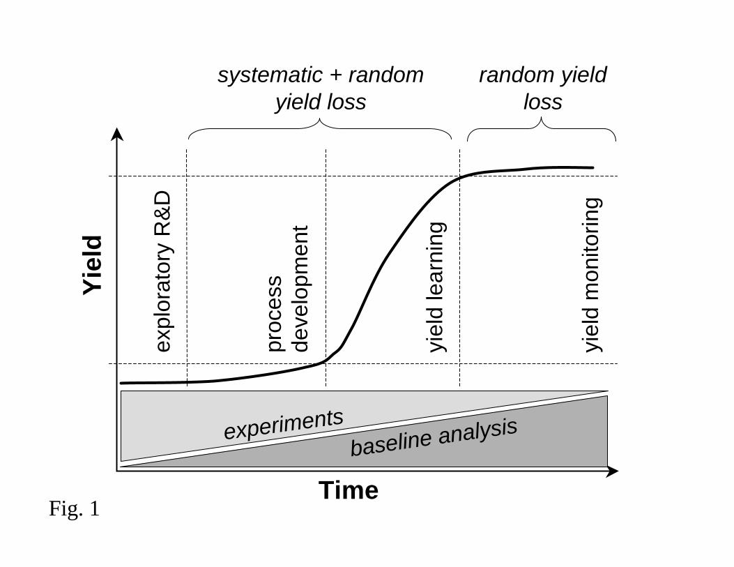
expl
orat
ory
R&
D
proc
ess
deve
lopm
ent
yiel
d le
arni
ng
yiel
d m
onito
ring
Yie
ld
Time
systematic + random yield loss
random yield loss
experimentsbaseline analysis
Fig. 1
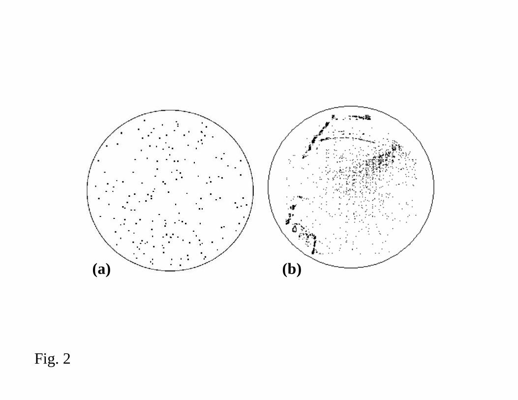
(a) (b)
Fig. 2
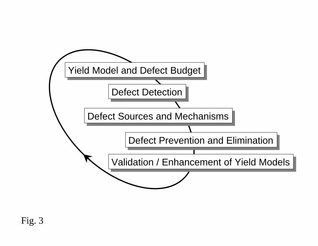
Yield Model and Defect BudgetYield Model and Defect Budget
Defect DetectionDefect Detection
Defect Sources and MechanismsDefect Sources and Mechanisms
Defect Prevention and EliminationDefect Prevention and Elimination
Validation / Enhancement of Yield ModelsValidation / Enhancement of Yield Models
Fig. 3
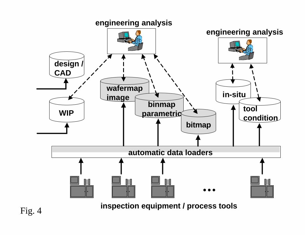
design / CAD
WIP
wafermap image
binmap parametric
bitmap
in-situ
tool condition
engineering analysisengineering analysis
inspection equipment / process tools
automatic data loaders
Fig. 4
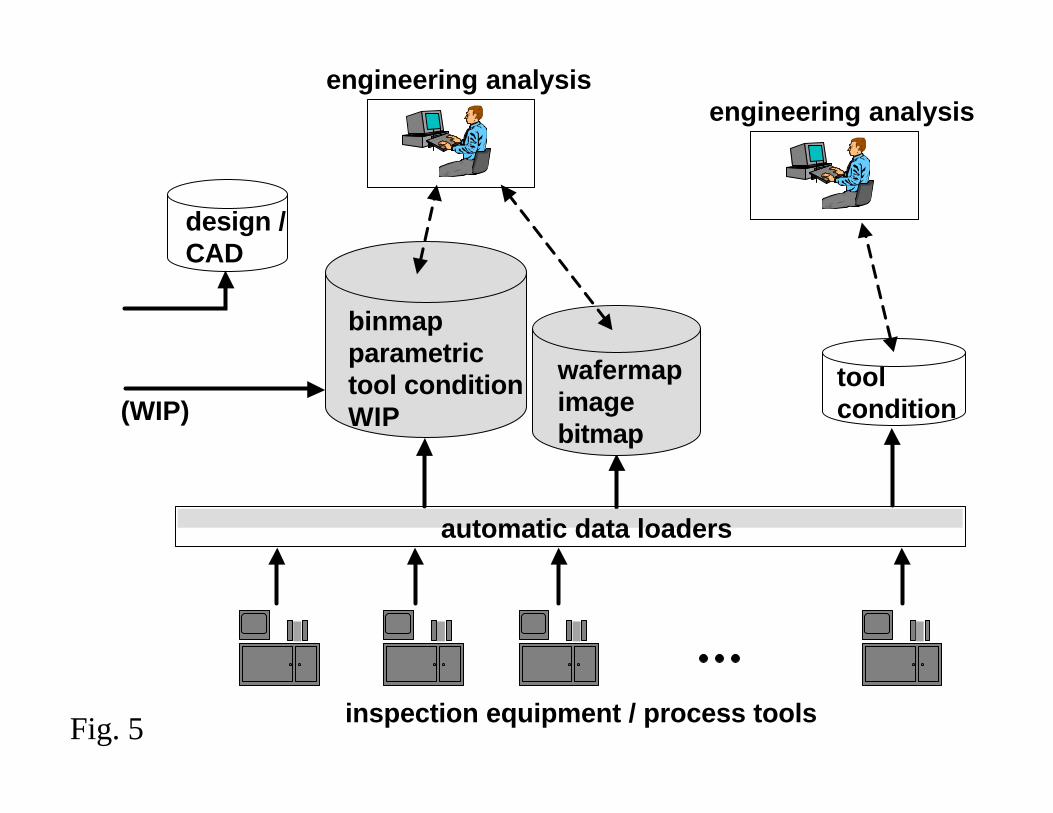
design / CAD
binmap parametric tool condition WIP
tool condition
engineering analysisengineering analysis
inspection equipment / process tools
wafermap image bitmap
(WIP)
automatic data loaders
Fig. 5
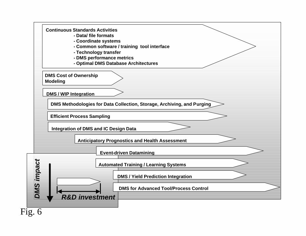
DM
S im
pac
t
R&D investment
Automated Training / Learning Systems
Continuous Standards Activities- Data/ file formats- Coordinate systems- Common software / training tool interface- Technology transfer- DMS performance metrics- Optimal DMS Database Architectures
DMS Cost of Ownership Modeling
DMS / WIP Integration
Anticipatory Prognostics and Health Assessment
DMS Methodologies for Data Collection, Storage, Archiving, and Purging
Efficient Process Sampling
Event-driven Datamining
DMS / Yield Prediction Integration
DMS for Advanced Tool/Process Control
Integration of DMS and IC Design Data
Fig. 6
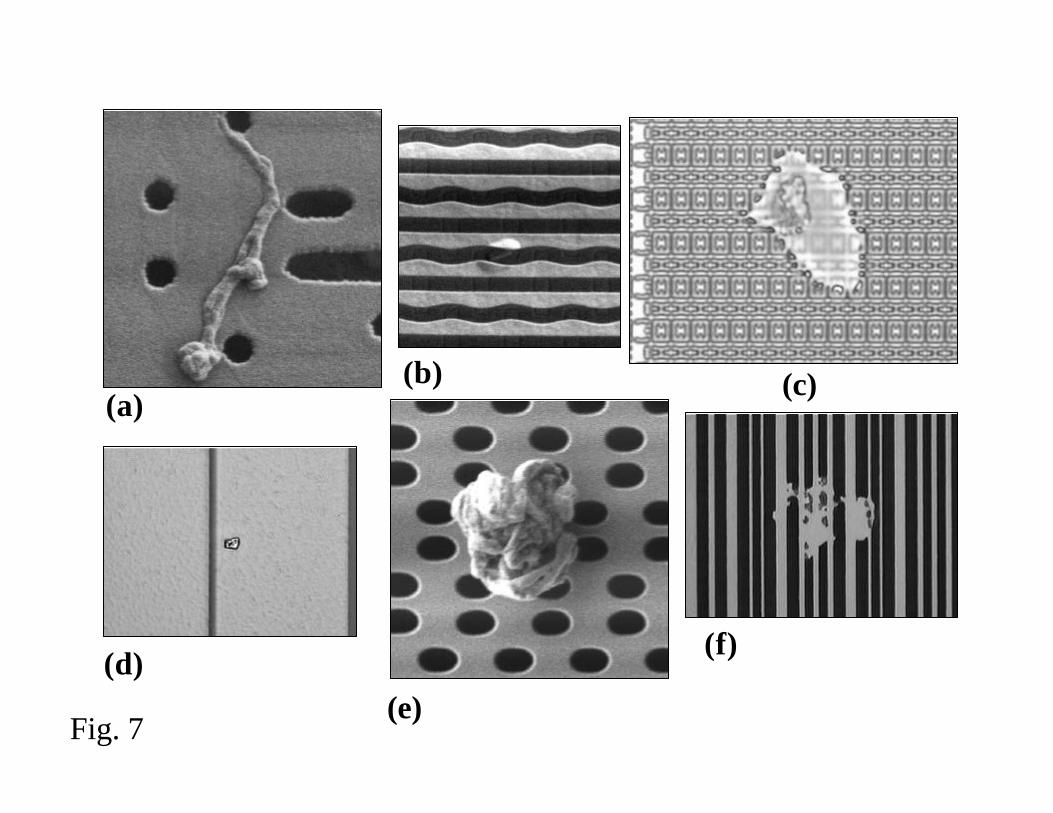
(a)(b) (c)
(d)(e)
(f)
Fig. 7
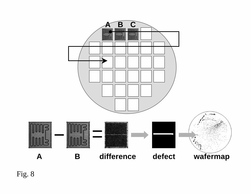
A B C
A B difference defect wafermap
Fig. 8
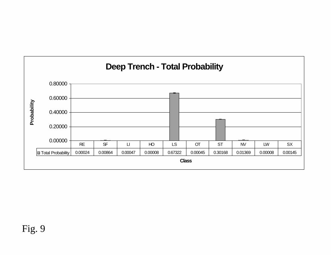
Deep Trench - Total Probability
0.00000
0.20000
0.40000
0.60000
0.80000
Class
Pro
bab
ility
Total Probability 0.00024 0.00864 0.00047 0.00008 0.67322 0.00045 0.30168 0.01369 0.00008 0.00145
RE SF LI HO LS OT ST NV LW SX
Fig. 9
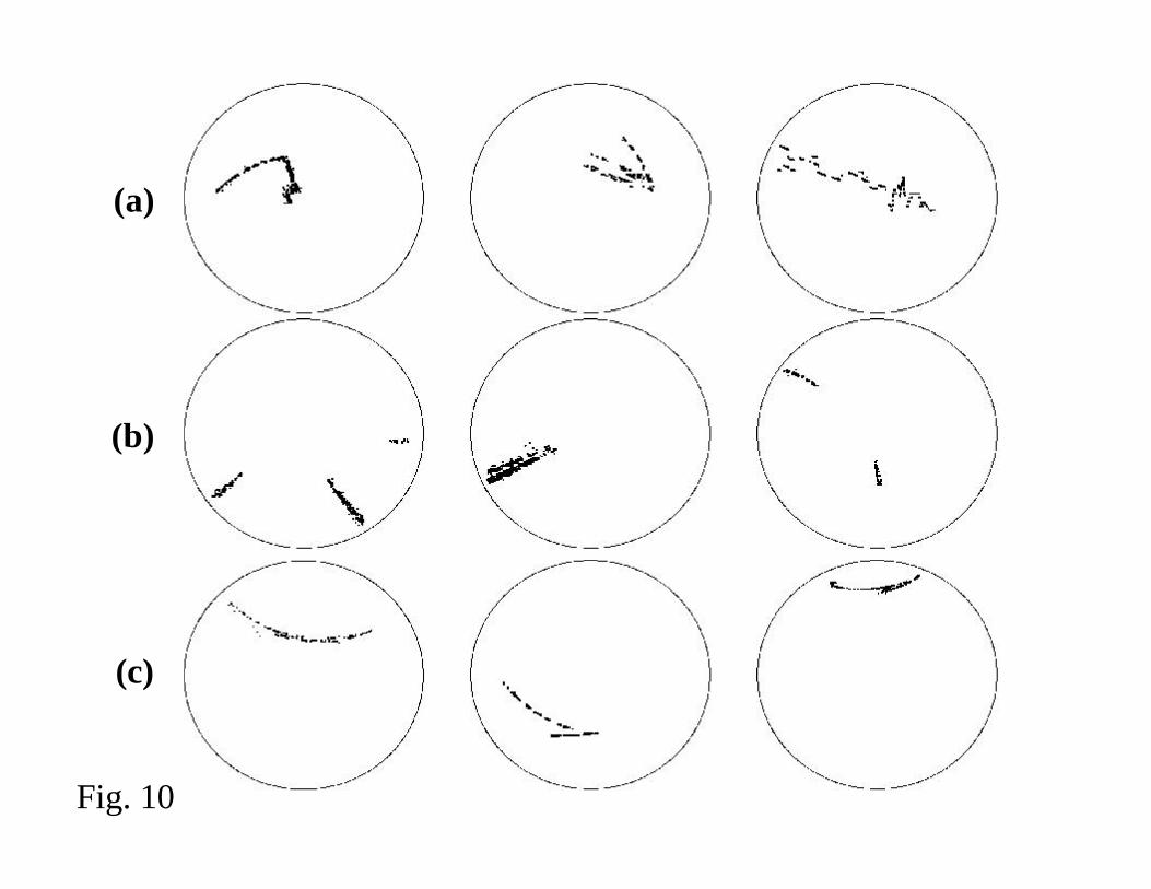
(a)
(b)
(c)
Fig. 10
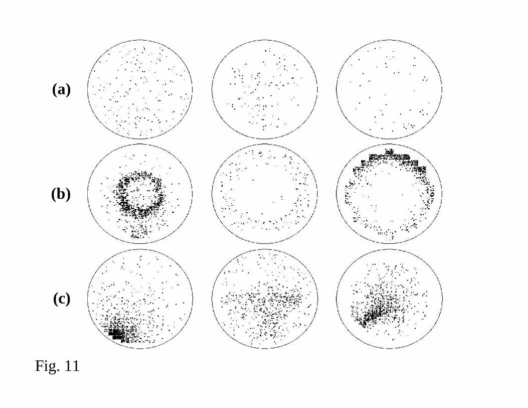
(a)
(b)
(c)
Fig. 11