2 Silicon: the Semiconductor Material - Princeton University · 2 Silicon: the Semiconductor...
18
2 Silicon: the Semiconductor Material W. Heywang, K.H. Zaininger 2.1 Introduction Fifty years of silicon for semiconductor device applications is the milestone at which this series of articles has been written, which will present the many- faceted development of all the technologies that are connected with it, their present status, and recognizable future trends. The individual articles will cover topics such as: – growth of single crystals and its reproducibility in industrial applications – polycrystalline and amorphous silicon – epitaxial technologies and thin films – crystal defects, impurities, and doping – various processes for micro- and nano-structuring – materials requirements from the vantage point of the users in the fields of microelectronics, power electronics, optoelectronics, and micromechanics – interfaces to other materials such as III–V compounds, as well as the whole area of bioelectronics. Since this series is about silicon it is taken as self-evident that all these contributions will emphasize the material aspects. This undertaking is justified and useful because silicon has, like no other material, dramatically changed our world. Especially, the whole of informa- tion and communication technology would have developed completely differ- ently without the availability of silicon. Thus, we can with all justification talk of a silicon era, just like one talks of a stone, copper, bronze, or iron age, where a specific material that predominantly characterized the advancements made during that time was chosen for the name of that era. Even more than with iron and steel, we have to deal here with a multitude of individual tech- nological advances which ultimately made the material as we know it today. The variety of the topics mentioned above attests to this. Last but not least, it has to be mentioned that silicon, because of the intense technological in- terest in it, belongs to the small group of solids that have been exhaustively studied and where, during its study, significant contributions to materials science have been made. We were invited to write an introductory paper to this series of articles be- cause we belong to those few people that have lived through this development
-
Upload
truongkhue -
Category
Documents
-
view
226 -
download
0
Transcript of 2 Silicon: the Semiconductor Material - Princeton University · 2 Silicon: the Semiconductor...
2 Silicon: the Semiconductor Material
W. Heywang, K.H. Zaininger
2.1 Introduction
Fifty years of silicon for semiconductor device applications is the milestoneat which this series of articles has been written, which will present the many-faceted development of all the technologies that are connected with it, theirpresent status, and recognizable future trends. The individual articles willcover topics such as:
– growth of single crystals and its reproducibility in industrial applications– polycrystalline and amorphous silicon– epitaxial technologies and thin films– crystal defects, impurities, and doping– various processes for micro- and nano-structuring– materials requirements from the vantage point of the users in the fields of
microelectronics, power electronics, optoelectronics, and micromechanics– interfaces to other materials such as III–V compounds, as well as the
whole area of bioelectronics.
Since this series is about silicon it is taken as self-evident that all thesecontributions will emphasize the material aspects.
This undertaking is justified and useful because silicon has, like no othermaterial, dramatically changed our world. Especially, the whole of informa-tion and communication technology would have developed completely differ-ently without the availability of silicon. Thus, we can with all justificationtalk of a silicon era, just like one talks of a stone, copper, bronze, or iron age,where a specific material that predominantly characterized the advancementsmade during that time was chosen for the name of that era. Even more thanwith iron and steel, we have to deal here with a multitude of individual tech-nological advances which ultimately made the material as we know it today.The variety of the topics mentioned above attests to this. Last but not least,it has to be mentioned that silicon, because of the intense technological in-terest in it, belongs to the small group of solids that have been exhaustivelystudied and where, during its study, significant contributions to materialsscience have been made.
We were invited to write an introductory paper to this series of articles be-cause we belong to those few people that have lived through this development
26 W. Heywang and K.H. Zaininger
from its very first beginnings – originally as technical–scientific researchersand later in responsible managerial positions. One of us (WH) was at Siemens,initially involved in the materials research and subsequently in device appli-cation. The other (KZ) was at RCA Laboratories in Princeton, NJ, USA,where he devoted his research efforts solely to silicon device technology. Wehave the indisputable advantage of a personal understanding of the variousproblems and an involvement in the sometimes dramatic happenings. On theother hand, there exists also the danger of a one-sided opinion. We believethat the advantage outweighs the disadvantage and that we can be ratherobjective; and so we have accepted this task.
In our discussion we want to show that silicon – during all of its develop-mental stages – in no way ever looked clearly to be the obvious solution tothe various problems as we so easily see it in retrospect today. On the con-trary, silicon’s march forward was often an adventurous path that had manyindividual successes, but also erroneous paths and fallacious assessments, asis common in all research- and development activities.
The silicon semiconductor technology formed the basis for the develop-ment of the information society, a society which is characterized by the mentalachievements of humankind. This partially virtual world – broken down intobits or built up from them – seems sometimes only a product of the humanbrain, a world made by humans. But still, where would this world be withoutsilicon?
Silicon does not appear as a free element in nature, because of its highchemical affinity, especially for oxygen. It can only be produced by chemicalreduction. Is it then also a product of man’s creativity, custom tailored forhis purpose? Or is it – with its special properties – still nothing else but awonderful present of nature?
2.2 Early History
When, in this contribution to Silicon, we talk about making silicon availablefor semiconductor applications, it is not just for history’s sake. No, we alsowant the readers to understand how this development was possible, whatparts were targeted goals, and what was simply serendipitous discovery? Herewe immediately come to the age-old question of humanity: Can man createhis own world – as often described or shown in some science fiction of ourtime – or is he still just embedded in this nature and creation that was givento us as a present?
Despite some fundamental work carried out in the 1920s and 1930s onthe band structure, and theoretical attempts concerning rectifier effects andseveral patents concerning the unipolar transistor in that period, the realsemiconductor era began only with the proof of the bipolar transistor effectin germanium by Bardeen and Brattain at the end of 1947 [1]. On the basis ofthe rapidly increasing industrial interest, the procedures for crystal growth,
2 Silicon: the Semiconductor Material 27
purification, and doping – still important even today – were then developedin the 1940s and 1950s, but initially just for germanium.
At the same time, an increased interest in other semiconductor materialsappeared. Were there perhaps materials other than germanium that wouldbe even more suitable for specific applications? This question could only beanswered by first understanding the transistor effect. The extremely highcarrier mobilities in germanium, about 103 higher than those of oxide semi-conductors, were fascinating here. Achieving even higher mobilities was thenone of the goals of the pioneering work in the field of III–V compounds byHeinrich Welker and his research team at the beginning of the 1950s [2].
Research on silicon began at about the same time, but rather in the back-ground. Sensational discoveries and/or advances were hardly expected unlessone considered the proof of the semiconducting character of silicon – still indoubt in the 1940s – as such. The metallic shine and relatively high conduc-tivity of the (highly impure) samples, similar to that in the so-called hardmetals, led to this erroneous conclusion. For example, in the 1953 edition ofLinus Pauling’s book General Chemistry [3], silicon is still called a semimetal.On the other hand, Pearson and Bardeen [4] had discovered in 1949 the high-temperature transition to intrinsic conduction and, thus, presented the proofof the semiconducting character of silicon. The samples used were, however,not single-crystal, so that the conductivity below this transition did not showthe typical temperature dependence of extrinsic semiconductor conductivity.This caused some irritation amongst the various researchers [5, 6].
The experiments of Pearson and Bardeen showed that the bandgap was1.12 eV. The carrier mobility could also be determined at the beginning of the1950s by use of Hall and drift measurements. With a value of 1200 cm2/V sfor electrons and 300 cm2/V s for holes, it was about a factor of three lowerthan that of germanium. All this did not seem to be very exciting, and thus,there were only a few researchers who devoted themselves to silicon and itscrystal growth.
Because of the increasing importance of microwaves in the mid-1940svarious semiconductor detectors, based partially polycrystalline silicon, wereused in microwave applications to replace microwave tubes because of theirsmall dimensions and high cut-off frequencies. So even at that time, siliconwas making inroads into communication technology. This was also where thenewly discovered transistor was of special interest, because a higher carriermobility is a definite advantage for achieving higher cut-off frequencies. So,a theoretical comparison – since the transistor effect in silicon was not yetexperimentally proven at that time – clearly indicated the advantage of ger-manium for use in communication technology, and the limit on the thermalstress of 80◦C, caused by the bandgap of only 0.7 eV, was considered accept-able. Only in cases of elevated heat production were these limitations serious,but it was hoped that they could be overcome by use of other semiconduc-tors such as the III–V compounds already mentioned or by silicon. The high
28 W. Heywang and K.H. Zaininger
degree of adaptability, the high carrier mobility (in GaAs, for example), anda lower melting point favorable for processing, were all strong arguments forthe III–V compounds. In silicon, on the other hand, one had to deal onlywith one kind of atom, which eliminates various kinds of lattice defects andguarantees a good lattice thermal conductivity.
So much for the theoretical considerations. In the reality of the techno-logical world of the early 1950s one was far away from a general use of siliconas a semiconductor material. As already mentioned, because of silicon’s highchemical aggressiveness at the elevated temperatures required for its prepa-ration, all silicon samples were highly impure. Their level of purity was, asPearson and Bardeen’s samples showed, in the range of several ppm. Despitethis, research groups, especially that of G.K. Teal at Bell Laboratories, werenot discouraged. Teal devoted himself, in addition to his main task of germa-nium, to silicon crystal growth until he went to Texas Instruments in 1952.But even there he built up a silicon research team which had the goal of devel-oping power transistors. The move to TI required time, and that significantlyreduced the original advantage he had over possible competitors.
2.3 Competition and Cooperation in the Silicon Race
At the beginning of the 1950s, but at first entirely in a clandestine mode,another competitor came onto the scene: the Siemens Group, of which WHwas a member. Despite entering late, Siemens definitely wanted to competein the important, newly blossoming area of semiconductor physics and tech-nology, having already its own manufacturing facility for selenium rectifiers,located in its power group; there was also a production facility for transistors,using its own experience base in high-frequency rectifiers and following BellLaboratories as far as germanium was concerned. With regard to additionalresearch, it had one of the best-known semiconductor pioneers, Walter Schot-tky, within its own ranks. For new semiconductors, Heinrich Welker, with hispioneering ideas and experience in III–V semiconductors, was appointed asdepartment head for the new research laboratories of Siemens-Schuckert.
In this technological environment, the materials research laboratory ofSiemens and Halske also entered the semiconductor area, and started in 1951to work mainly on trial-and-error experiments on silicides such as Mg2Si.The purification of silicon was included as a prerequisite in these fundamen-tal studies. To achieve this, two approaches were pursued: on the one handthe classical metallurgical preparation of pure silicon powder via magnesiumor zinc reduction of pure quartz (the so-called B-process), and on the otherhand the reduction of SiHCl3 by hydrogen in an electrical discharge accord-ing to the method of van Arkel. This second approach was carried out incollaboration with Wiberg and Amberger of the University of Munich andwas called the A-process.
2 Silicon: the Semiconductor Material 29
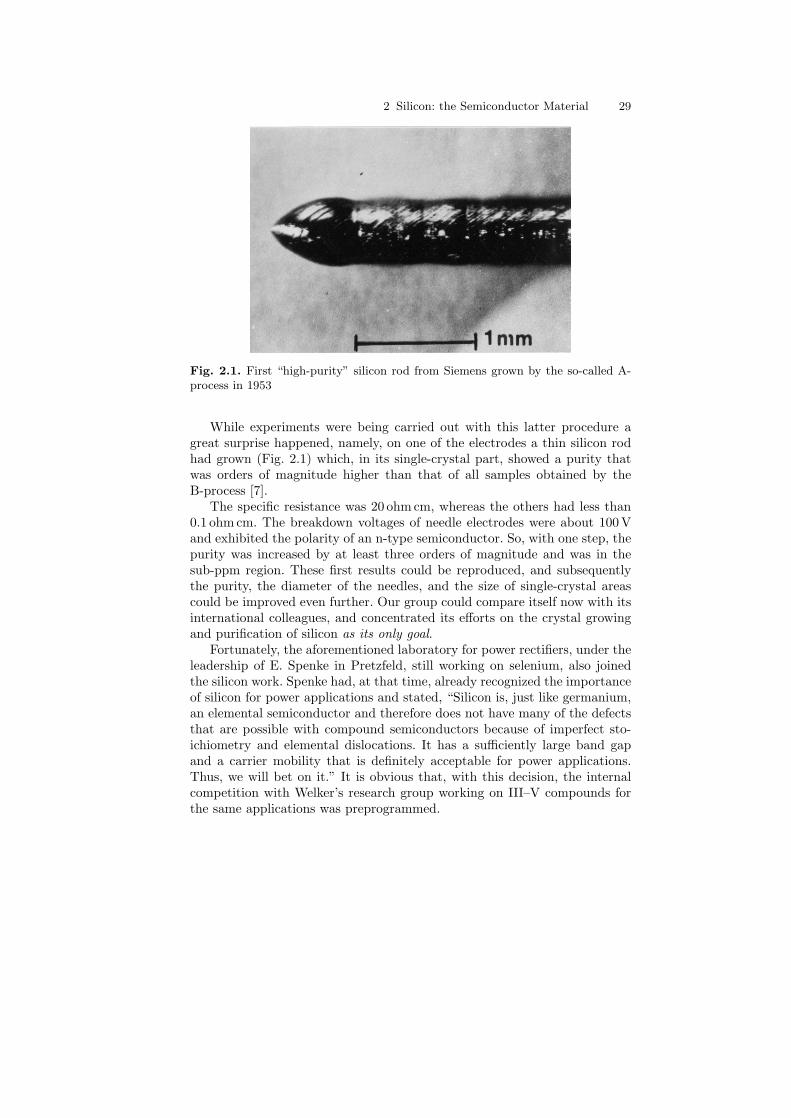
Fig. 2.1. First “high-purity” silicon rod from Siemens grown by the so-called A-process in 1953
While experiments were being carried out with this latter procedure agreat surprise happened, namely, on one of the electrodes a thin silicon rodhad grown (Fig. 2.1) which, in its single-crystal part, showed a purity thatwas orders of magnitude higher than that of all samples obtained by theB-process [7].
The specific resistance was 20 ohm cm, whereas the others had less than0.1 ohm cm. The breakdown voltages of needle electrodes were about 100 Vand exhibited the polarity of an n-type semiconductor. So, with one step, thepurity was increased by at least three orders of magnitude and was in thesub-ppm region. These first results could be reproduced, and subsequentlythe purity, the diameter of the needles, and the size of single-crystal areascould be improved even further. Our group could compare itself now with itsinternational colleagues, and concentrated its efforts on the crystal growingand purification of silicon as its only goal.
Fortunately, the aforementioned laboratory for power rectifiers, under theleadership of E. Spenke in Pretzfeld, still working on selenium, also joinedthe silicon work. Spenke had, at that time, already recognized the importanceof silicon for power applications and stated, “Silicon is, just like germanium,an elemental semiconductor and therefore does not have many of the defectsthat are possible with compound semiconductors because of imperfect sto-ichiometry and elemental dislocations. It has a sufficiently large band gapand a carrier mobility that is definitely acceptable for power applications.Thus, we will bet on it.” It is obvious that, with this decision, the internalcompetition with Welker’s research group working on III–V compounds forthe same applications was preprogrammed.
30 W. Heywang and K.H. Zaininger
In Spenke’s remarkable prognosis, made in 1953, one important charac-teristic of silicon is understandably not mentioned, namely the long carrierlifetime. This is a result of the specific band structure of silicon, which itshares with germanium, but was not yet known at that time, namely thatthe minimum of the conduction band – contrary to the original assumption– does not occur at the wave vector k = 0 but, rather, near the edge of theBrillouin zone. This prevents a direct optical recombination of electrons andholes, which would occur in a time on the order of magnitude of 1 microsec-ond (as, for example, in GaAs). This, of course, prevents, on the one hand,the technological use of silicon in the area of active light generation but al-lows, on the other hand, the achievement of long carrier lifetimes (just as ingermanium) for high purity and perfect crystallinity. This gift of nature wasa crucial (at that time of course unknown) precondition for the discovery anddevelopment of the bipolar germanium transistor, because it is the means forachieving the required diffusion lengths of minority carriers. High diffusionlengths are important factors for the I–V characteristics not only of bipolartransistors but also of all power devices such as rectifiers and thyristors.
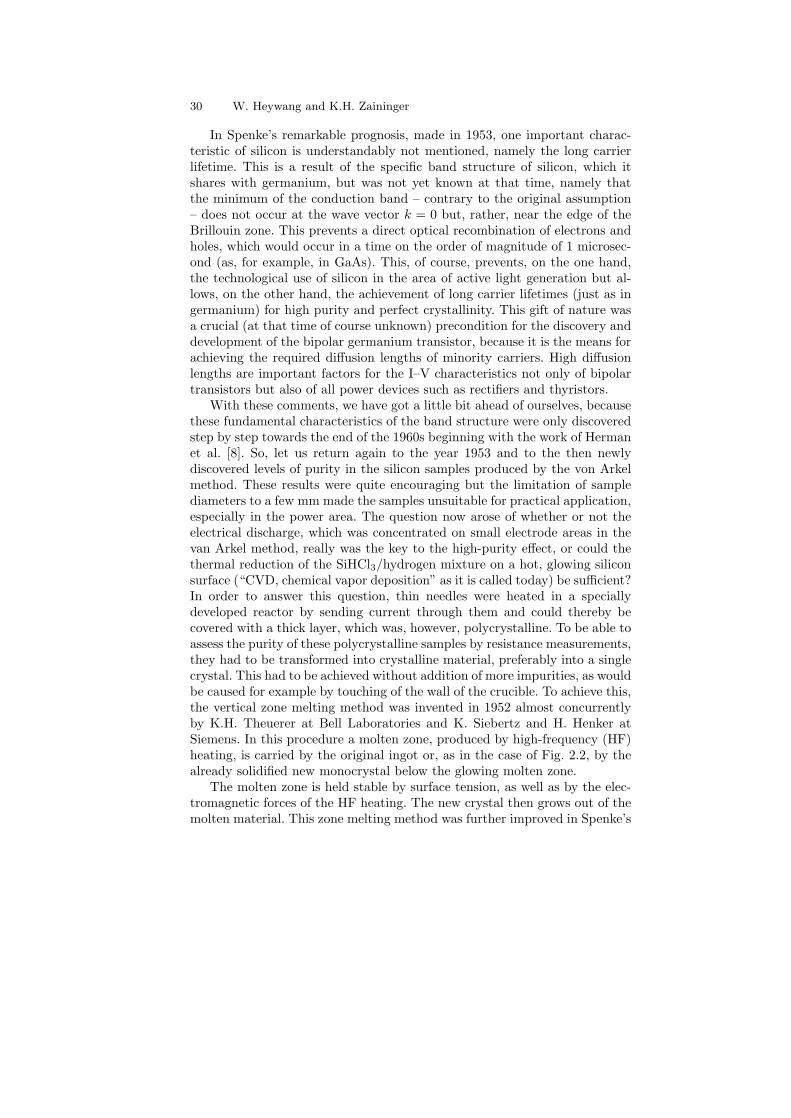
With these comments, we have got a little bit ahead of ourselves, becausethese fundamental characteristics of the band structure were only discoveredstep by step towards the end of the 1960s beginning with the work of Hermanet al. [8]. So, let us return again to the year 1953 and to the then newlydiscovered levels of purity in the silicon samples produced by the von Arkelmethod. These results were quite encouraging but the limitation of samplediameters to a few mm made the samples unsuitable for practical application,especially in the power area. The question now arose of whether or not theelectrical discharge, which was concentrated on small electrode areas in thevan Arkel method, really was the key to the high-purity effect, or could thethermal reduction of the SiHCl3/hydrogen mixture on a hot, glowing siliconsurface (“CVD, chemical vapor deposition” as it is called today) be sufficient?In order to answer this question, thin needles were heated in a speciallydeveloped reactor by sending current through them and could thereby becovered with a thick layer, which was, however, polycrystalline. To be able toassess the purity of these polycrystalline samples by resistance measurements,they had to be transformed into crystalline material, preferably into a singlecrystal. This had to be achieved without addition of more impurities, as wouldbe caused for example by touching of the wall of the crucible. To achieve this,the vertical zone melting method was invented in 1952 almost concurrentlyby K.H. Theuerer at Bell Laboratories and K. Siebertz and H. Henker atSiemens. In this procedure a molten zone, produced by high-frequency (HF)heating, is carried by the original ingot or, as in the case of Fig. 2.2, by thealready solidified new monocrystal below the glowing molten zone.
The molten zone is held stable by surface tension, as well as by the elec-tromagnetic forces of the HF heating. The new crystal then grows out of themolten material. This zone melting method was further improved in Spenke’s
2 Silicon: the Semiconductor Material 31
Fig. 2.2. Vertical zone melting (courtesy Wacker Chemitronics)
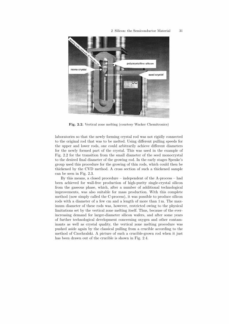
laboratories so that the newly forming crystal rod was not rigidly connectedto the original rod that was to be melted. Using different pulling speeds forthe upper and lower rods, one could arbitrarily achieve different diametersfor the newly formed part of the crystal. This was used in the example ofFig. 2.2 for the transition from the small diameter of the seed monocrystalto the desired final diameter of the growing rod. In the early stages Spenke’sgroup used this procedure for the growing of thin rods, which could then bethickened by the CVD method. A cross section of such a thickened samplecan be seen in Fig. 2.3.
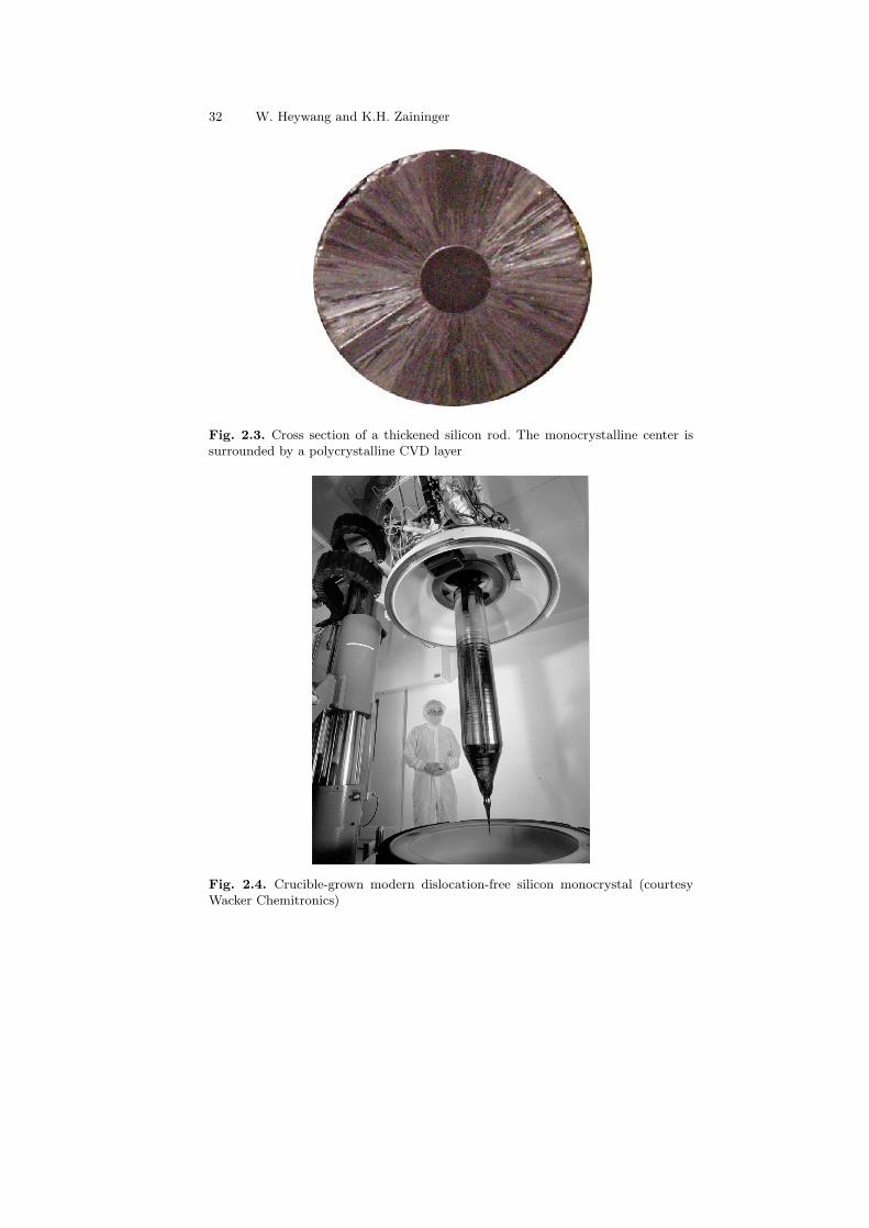
By this means, a closed procedure – independent of the A-process – hadbeen achieved for wall-free production of high-purity single-crystal siliconfrom the gaseous phase, which, after a number of additional technologicalimprovements, was also suitable for mass production. With this completemethod (now simply called the C-process), it was possible to produce siliconrods with a diameter of a few cm and a length of more than 1 m. The max-imum diameter of these rods was, however, restricted owing to the physicallimitations set by the vertical zone melting itself. Thus, because of the ever-increasing demand for larger-diameter silicon wafers, and after some yearsof further technological development concerning oxygen and other contam-inants as well as crystal quality, the vertical zone melting procedure waspushed aside again by the classical pulling from a crucible according to themethod of Czochralski. A picture of such a crucible-grown rod when it justhas been drawn out of the crucible is shown in Fig. 2.4.
32 W. Heywang and K.H. Zaininger
Fig. 2.3. Cross section of a thickened silicon rod. The monocrystalline center issurrounded by a polycrystalline CVD layer
Fig. 2.4. Crucible-grown modern dislocation-free silicon monocrystal (courtesyWacker Chemitronics)
2 Silicon: the Semiconductor Material 33
Nevertheless, the development of the vertical zone melting process was,at that time, an absolutely necessary step for the industrial breakthrough ofsilicon as a semiconductor material. The complete C-process had opened theway to industrial mass production.
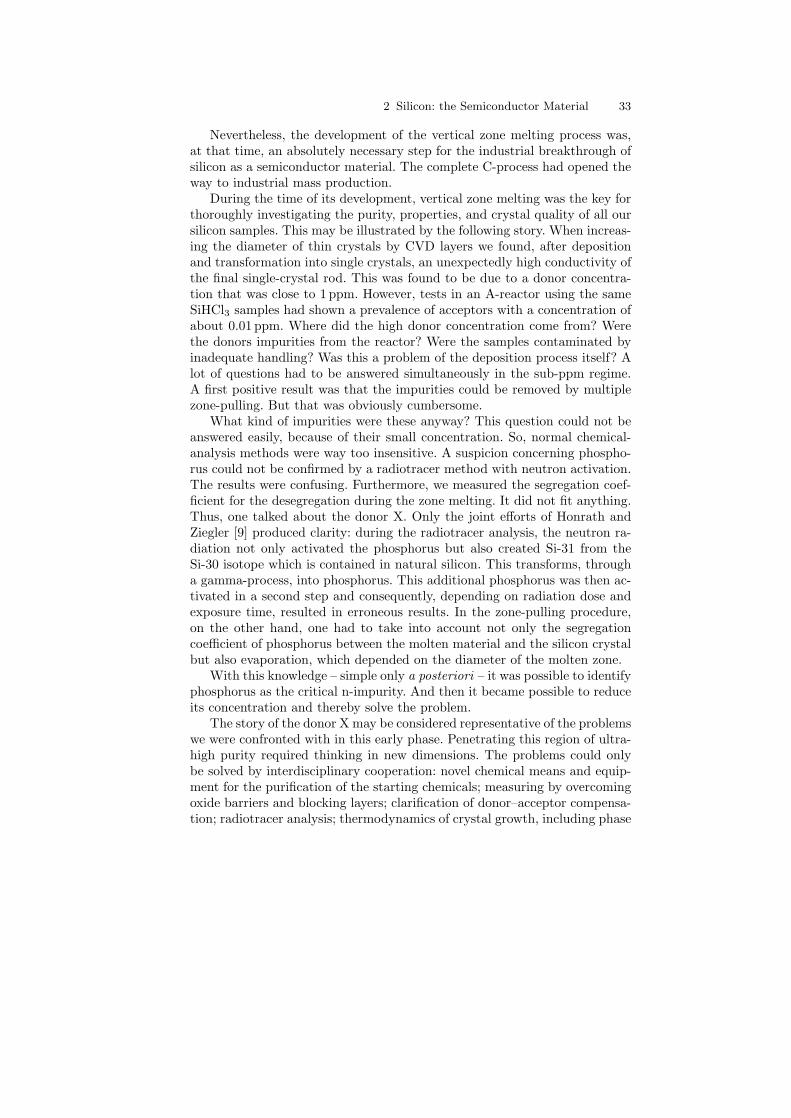
During the time of its development, vertical zone melting was the key forthoroughly investigating the purity, properties, and crystal quality of all oursilicon samples. This may be illustrated by the following story. When increas-ing the diameter of thin crystals by CVD layers we found, after depositionand transformation into single crystals, an unexpectedly high conductivity ofthe final single-crystal rod. This was found to be due to a donor concentra-tion that was close to 1 ppm. However, tests in an A-reactor using the sameSiHCl3 samples had shown a prevalence of acceptors with a concentration ofabout 0.01 ppm. Where did the high donor concentration come from? Werethe donors impurities from the reactor? Were the samples contaminated byinadequate handling? Was this a problem of the deposition process itself? Alot of questions had to be answered simultaneously in the sub-ppm regime.A first positive result was that the impurities could be removed by multiplezone-pulling. But that was obviously cumbersome.
What kind of impurities were these anyway? This question could not beanswered easily, because of their small concentration. So, normal chemical-analysis methods were way too insensitive. A suspicion concerning phospho-rus could not be confirmed by a radiotracer method with neutron activation.The results were confusing. Furthermore, we measured the segregation coef-ficient for the desegregation during the zone melting. It did not fit anything.Thus, one talked about the donor X. Only the joint efforts of Honrath andZiegler [9] produced clarity: during the radiotracer analysis, the neutron ra-diation not only activated the phosphorus but also created Si-31 from theSi-30 isotope which is contained in natural silicon. This transforms, througha gamma-process, into phosphorus. This additional phosphorus was then ac-tivated in a second step and consequently, depending on radiation dose andexposure time, resulted in erroneous results. In the zone-pulling procedure,on the other hand, one had to take into account not only the segregationcoefficient of phosphorus between the molten material and the silicon crystalbut also evaporation, which depended on the diameter of the molten zone.
With this knowledge – simple only a posteriori – it was possible to identifyphosphorus as the critical n-impurity. And then it became possible to reduceits concentration and thereby solve the problem.
The story of the donor X may be considered representative of the problemswe were confronted with in this early phase. Penetrating this region of ultra-high purity required thinking in new dimensions. The problems could onlybe solved by interdisciplinary cooperation: novel chemical means and equip-ment for the purification of the starting chemicals; measuring by overcomingoxide barriers and blocking layers; clarification of donor–acceptor compensa-tion; radiotracer analysis; thermodynamics of crystal growth, including phase
34 W. Heywang and K.H. Zaininger
diagrams; interactions between the various contaminants and with lattice de-fects; etc. Thus, it is obvious that a close cooperation had to be developedbetween the different Siemens groups on the one hand and the suppliers ofthe chemical substances on the other hand. This mainly concerned the metal–organic compounds of the Si–H–Cl system. There was a continuous exchangeof samples and data between our different groups on the one hand and Wacker(later on Wacker-Chemitronics) on the other hand. This cooperation had, atfirst, developed open-mindedly but then it was formalized and, finally, it ledto a licensing agreement for the entire production and test process.
Two special results of this early company cooperation should be men-tioned:
– The boron problem: boron is an acceptor dopant still in use for device pro-duction. In contrast to phosphorus, it cannot be removed by zone refiningor evaporation, because of its chemical similarity to silicon. Thus we hadto rely entirely on Wacker’s purification process and reliability.
– The carbon problem: chemically, carbon is homologous to silicon and doesnot act as a donor or acceptor; it cannot be detected by resistivity measure-ment. But, through the formation of SiC precipitates, it prevents monocrys-talline crystal growth. These SiC precipitates were the result of SiHCl2CH3contamination of SiHCl3. Again, we depended here entirely on the capa-bility and quality control of Wacker.
There was also some work on silicon at IBM in Schwuttke’s group. How-ever, it did not result in many pivotal advances in the field of very puresilicon. The contributions were more along the lines of crystal defect analysisby x-ray topography.
These few examples from the early cooperative efforts may underline againthat the development process described above was an expedition into the un-known that could have easily gone astray. But high-purity, perfect siliconcrystals are not a purpose in themselves; they represent a crucial precon-dition for the proper functioning of semiconductor devices, which, in turn,are a result of proper doping, structuring, contacting, etc. All of this formsa separate set of problems, which had to be gotten under control throughrelevant research and development. These topics will be treated in separatecontributions within the framework of this series, so that we do not have togo into details in this introduction.
2.4 Initial Device Applications
It seems significant to us that the Texas Instruments and Siemens groups,which worked independently on silicon, had also set themselves different goals.The main goal of Teal was the development of bipolar silicon transistors. Heshowed initial results at the 1954 IRE Conference in Dayton during his pre-sentation “Some recent developments in silicon and germanium materials and
2 Silicon: the Semiconductor Material 35
devices.” But, as he stated himself in 1976 in his survey article [10], he couldhardly overcome the existing reservations concerning the reproducibility andstability of silicon transistors. In addition, there was a lower cut-off frequencydue to the lower carrier mobility for comparable geometries. This did not,however, deter him from continuing to pursue this approach, especially formilitary applications that had higher power requirements.
Concerning the application of silicon in communication and informationtechnology Siemens (at that time Siemens & Halske) remained sceptical de-spite the advances in the development of the highest-purity silicon – followingthe philosophy of Bell Laboratories. Only at Siemens-Schuckert (responsiblefor power technology) did Spenke and his group devote themselves consis-tently to the development and technical improvement of silicon for commer-cial application in high-power rectifiers in order to replace the old seleniumtechnology. This new approach, including device technology, was ready in1956 for application and was used at first for power rectifiers in Siemens loco-motives [11]. Obviously, the total internal Siemens power-electric market wasimmediately available for the application of these rectifiers – an advantage notto be underestimated. Contrary to other companies, Siemens did not pursue apolicy of a monopoly in the silicon market, but rather gave licenses for the to-tal high-purity silicon manufacturing process not only to Wacker in Germanybut also to other chemical companies, mainly in the USA and Japan. Theselicensing agreements also included cooperation, so that further improvementscould be exchanged, and some kind of worldwide cooperation developed. Thishad the consequence that one can say today that the total world productionof silicon semiconductor material was initiated by the so-called Siemens Pro-cess. An example of a modern silicon rod can be seen in Fig. 2.4 and shouldbe compared with the mini-rod of half a century ago (Fig. 2.1).
As far as commercial power applications were concerned, Siemens obvi-ously did not stop with the development of silicon rectifiers; transistors andthyristors were also developed. Here, they encountered the same problemof instability in the I–V characteristics that Texas Instruments had alreadyseen. One of the important concerns was related to the trapping problem,i.e. the time-limited presence of charge carriers at defect sites. Bell Labora-tories had already encountered this problem in 1953 during the examinationof their silicon [12]. Was this trapping effect possibly due to “natural” de-fects that were intrinsic to silicon and therefore unavoidable, for example,lattice defects? We also attacked this problem and thoroughly examined var-ious trapping effects in the silicon that was produced in Spenke’s laboratoriesand also elsewhere [13,14]. The most important result of those investigationswas that the trap density in the silicon produced by the Siemens process wasbelow 1011/cm3 and, therefore, caused no problem at room temperature. Thereason for that was the absolutely wall-free preparation of this silicon – anadvantage not planned but nevertheless crucial.
36 W. Heywang and K.H. Zaininger
2.5 MOS Technology and Integration
Despite all these above-mentioned encouraging results at Texas Instrumentsand Siemens, the breakthrough for the use of silicon instead of germanium inthe communication and information area was not at all guaranteed yet. Evenat the end of the 1950s, higher cut-off frequencies seemed to be the deter-mining factor. The higher carrier mobilities found in Ge and GaAs were farmore attractive. The breakthrough of silicon came only with two innovationswhich were unexpected to most semiconductor specialists:
1. The discovery that thermally grown SiO2 films passivate (stabilize) thesurface of the silicon substrate was the turning point in semiconductortechnology resulting in the change from germanium to silicon, since ger-manium surfaces could not be stabilized in a similar manner. This passi-vation was due to a significant reduction of the surface states (dangling Sisurface bonds) by forming Si-surface–O bonds and made possible the con-trol of charge carriers via the oxide layer. The low density of surface statesin Si–SiO2 structures opened up the way for developing the metal–oxide(SiO2)–semiconductor (Si) field-effect transistor (MOSFET), which, inits basic concept, utilizes ideas that were already known in the 1920s(e.g. [15]), but which were at that time miles away from being able to berealized. In the development of this technology, which is today the basisfor microchips, especially those used in computers, the properties of theSiO2 film as a dielectric and mechanical layer also played an importantrole.
The first realization of an MOS transistor was achieved in 1960 byKahng and Atalla at Bell Laboratories [16] and was followed in 1961 byZaininger at RCA Laboratories [17]. But it still required a large amount ofadditional developmental work until the MOS transistor technology wasunder control and reproducible. This will be treated in detail in one ofthe following articles. Therefore we shall limit ourselves to simply point-ing out that, before the development of the MOS technology, it was adownright statement of faith that stable semiconductor devices had toavoid or at least to fight the detrimental influence of the surface.
2. The second innovation is also related to the surface. It is the concept ofdevice integration within a single silicon chip, which, at its beginning,seemed to many rather limited in its possibilities. One has to rememberthat the yield for single transistors at that time was about 30%. Thus, bysimple deduction one would expect the yield for two hard-wired transis-tors to be 0.3×0.3, i.e. about 10%, for three transistors about 3%, and soon. It was Kilby’s brilliant mind [18] which realized that it is really themetal wire connection that is the main source of failures and that avoid-ing it by “integrating” could lead to higher yield and reliability. Indeed,he built the first functioning integrated circuits, initially a phase shiftoscillator and then a few flip-flops, in the summer of 1957 by connecting
2 Silicon: the Semiconductor Material 37
about 25 transistors that were on a 5 inch germanium wafer. But who atthat time would have seriously thought of the high levels of integrationthat are characteristic of today’s microelectronics? These developmentswould not have been imaginable without the specific masking propertiesof the silicon dioxide layer. Since this question, together with the manyrequired research topics and technological developments, will be discussedin detail in the following articles, we shall limit ourselves to just this onequestion. Which properties of silicon are crucial for the role of the siliconoxide layer?
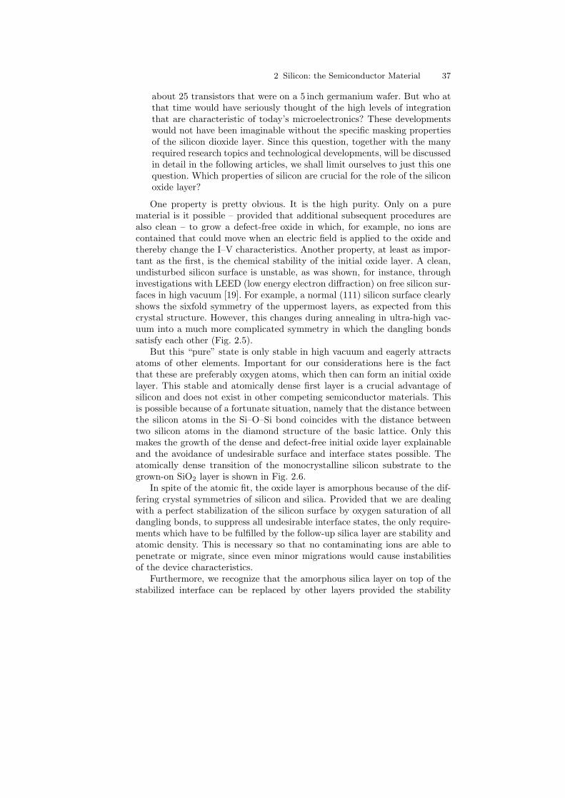
One property is pretty obvious. It is the high purity. Only on a purematerial is it possible – provided that additional subsequent procedures arealso clean – to grow a defect-free oxide in which, for example, no ions arecontained that could move when an electric field is applied to the oxide andthereby change the I–V characteristics. Another property, at least as impor-tant as the first, is the chemical stability of the initial oxide layer. A clean,undisturbed silicon surface is unstable, as was shown, for instance, throughinvestigations with LEED (low energy electron diffraction) on free silicon sur-faces in high vacuum [19]. For example, a normal (111) silicon surface clearlyshows the sixfold symmetry of the uppermost layers, as expected from thiscrystal structure. However, this changes during annealing in ultra-high vac-uum into a much more complicated symmetry in which the dangling bondssatisfy each other (Fig. 2.5).
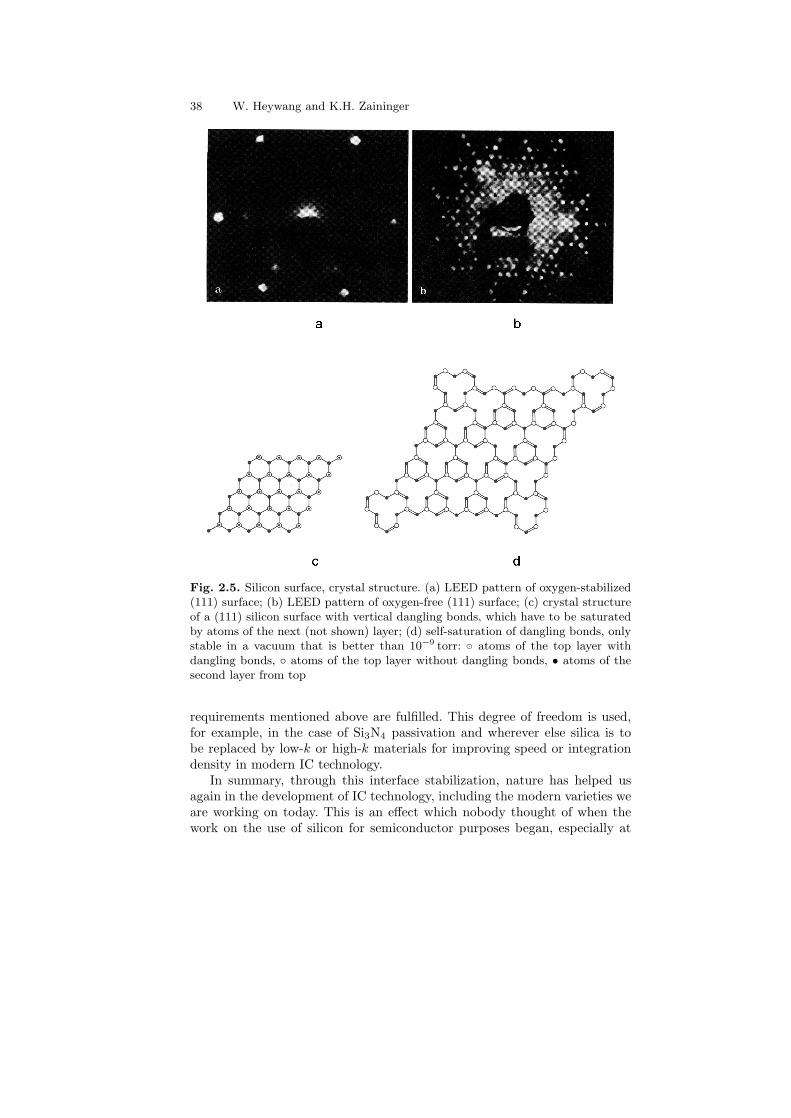
But this “pure” state is only stable in high vacuum and eagerly attractsatoms of other elements. Important for our considerations here is the factthat these are preferably oxygen atoms, which then can form an initial oxidelayer. This stable and atomically dense first layer is a crucial advantage ofsilicon and does not exist in other competing semiconductor materials. Thisis possible because of a fortunate situation, namely that the distance betweenthe silicon atoms in the Si–O–Si bond coincides with the distance betweentwo silicon atoms in the diamond structure of the basic lattice. Only thismakes the growth of the dense and defect-free initial oxide layer explainableand the avoidance of undesirable surface and interface states possible. Theatomically dense transition of the monocrystalline silicon substrate to thegrown-on SiO2 layer is shown in Fig. 2.6.
In spite of the atomic fit, the oxide layer is amorphous because of the dif-fering crystal symmetries of silicon and silica. Provided that we are dealingwith a perfect stabilization of the silicon surface by oxygen saturation of alldangling bonds, to suppress all undesirable interface states, the only require-ments which have to be fulfilled by the follow-up silica layer are stability andatomic density. This is necessary so that no contaminating ions are able topenetrate or migrate, since even minor migrations would cause instabilitiesof the device characteristics.
Furthermore, we recognize that the amorphous silica layer on top of thestabilized interface can be replaced by other layers provided the stability
38 W. Heywang and K.H. Zaininger
Fig. 2.5. Silicon surface, crystal structure. (a) LEED pattern of oxygen-stabilized(111) surface; (b) LEED pattern of oxygen-free (111) surface; (c) crystal structureof a (111) silicon surface with vertical dangling bonds, which have to be saturatedby atoms of the next (not shown) layer; (d) self-saturation of dangling bonds, onlystable in a vacuum that is better than 10−9 torr: ⊙ atoms of the top layer withdangling bonds, ◦ atoms of the top layer without dangling bonds, • atoms of thesecond layer from top
requirements mentioned above are fulfilled. This degree of freedom is used,for example, in the case of Si3N4 passivation and wherever else silica is tobe replaced by low-k or high-k materials for improving speed or integrationdensity in modern IC technology.
In summary, through this interface stabilization, nature has helped usagain in the development of IC technology, including the modern varieties weare working on today. This is an effect which nobody thought of when thework on the use of silicon for semiconductor purposes began, especially at
2 Silicon: the Semiconductor Material 39
Fig. 2.6. Interface between silicon substrate and SiO2 surface layer in atomicresolution
a time when there were so many other problems connected with the alwayspresent oxide layer during measurements and contact making.
Finally, the following fact, which was crucial for the victorious advanceof silicon into information technology, has to be pointed out. Advanced MOSTechnology and very large-scale integration (VLSI) – both based on the ex-traordinary properties of the Si–SiO2 system – opened the way for a cost-effective digital technology, which then, in turn, opened the way for thenecessary mass market in silicon integrated circuits for use in informationtechnology.
2.6 Conclusion
With these remarks, which already reach into the heart of the silicon era, wewant to conclude this review of the pioneering times of silicon, the semicon-ductor material. We hope that this description of the whole development ofpure, single-crystal silicon makes three things clear:
1. Silicon, with all its positive basic attributes, had first to be made read-ily available for large-scale common use. This was an often difficult pathinto the unknown, where only the human pioneering spirit had a chanceto overcome all the difficulties that were encountered. It certainly wasnot a straightforward development – as it might appear to someone inretrospect and as extrapolations such as Moore’s Law might make onebelieve – but rather one that was characterized by many, often extremelycomplex individual developments. It was an outstanding achievement ofthe human spirit in research, as well as of interdisciplinary cooperationbetween material researchers, device developers, designers, and technol-ogists.
40 W. Heywang and K.H. Zaininger
2. Most importantly, it is obvious that a uniform, high-purity, perfect single-crystal piece of silicon material alone would be of extremely limited tech-nological use. It is only when this material is suitably altered and struc-tured through controlled, reproducible processes and then made into use-ful devices that it becomes valuable. All of these requirements could nothave been achieved were it not for the fact that nature provided us withan extraordinary gift, through suitable physical properties and constants,etc. – an abundance of wonderful, often crucial properties and character-istics of silicon, silicon dioxide, and the Si–SiO2 interface that, together,make modern integrated silicon technology possible at all. Let us justquickly enumerate the most important properties and characteristics:
2.6.1 Silicon
– Abundant: easy to obtain, low cost.– Single crystal: with ever larger rod diameters (30 cm). Defects can be
eliminated or selectively utilized for advantage.– Not brittle: can easily be handled and is an excellent mechanical substrate
for individual devices and integrated circuit chips.– Adequate thermal conductivity to take away the electrically generated
heat in chips.– Can be microstructured by a combination of suitable optical and chemical
methods (lithography), even breaking through the 0.1 micron barrier.– Thin crystalline silicon films with different electrical properties can be
grown onto silicon substrates via epitaxy.– Thin crystalline silicon films with various electrical properties can be
grown onto insulators (sapphire, etc.) to provide improved isolation andspeed, and lower capacitance.
– Thin crystalline germanium films and, probably, novel films of III–V com-pounds containing quantum dots, offering different electrical and opticalproperties, can be grown onto silicon substrates via chemical vapor depo-sition or molecular-beam epitaxy.
– Buried thin films of SiO2 can be created under the silicon surface byoxygen ion implantation and subsequent annealing (SIMOX structures).
– Has a very useful energy gap (1.12 eV).– Conductivity can be tailored (n-type, p-type, value) by doping using dif-
fusion and/or ion implantation.– As an elemental semiconductor, it does not have the multitude of ma-
terials problems and chemical behavior that compound semiconductorshave.
– Annealing works very well.– Carrier mobility is good for both electrons and holes (important in CMOS
circuits).
2 Silicon: the Semiconductor Material 41
– Carrier lifetime for both electrons and holes is good because of specialband structure properties and low density of traps (important for bi-polardevices).
– Not light-sensitive (stable operation of devices under various light condi-tions).
2.6.2 Silicon Dioxide [20]
– Can be thermally grown as a native oxide by a simple, inexpensive andreliable (oxidation) process.
– Can be deposited via chemical vapor deposition and other methods.– Is stable up to very high temperatures (important for annealing).– Films can be very thin (100 A) (necessary for ultrasmall MOS devices).– Acts as a chemical barrier during etching of selected silicon areas,– Can act as a diffusion barrier for certain materials, especially most of the
common dopants.– Acts as a barrier during ion implantation.– Is chemically stable but can be microstructured by a combination of suit-
able optical and chemical methods (lithography), even breaking throughthe 0.1 micron barrier.
– Metal patterns, deposited on it by various methods, adhere very well.– Is mechanically strong and can act as a protective layer (physical and
ionic protection).– Can be polished to planarize the surface.– Is transparent.– High electrical breakdown strength.– Useful dielectric constant (but here there is a need for new insulating
materials to replace SiO2 in certain areas: high-k materials for the gateand low-k materials for insulating the wiring).
2.6.3 Si–SiO2 Interface [21]
– Has an extremely low density of interface states when properly prepared.– Very stable.
Had this been different – either through a quirk of nature or a dispensationof providence – the development would have taken a different path, and theenormous advances we see today, especially in microelectronics and informa-tion technology, would hardly be imaginable.
3. As outlined in item 2 above, silicon is a unique gift of nature, so thatwe are justified in speaking of the semiconductor material. It cannot besupplanted in its importance to our technology and will continue to dom-inate the core of semiconductor electronics. Important complementarytechnologies can only be expected in areas where silicon encounters its
42 W. Heywang and K.H. Zaininger
natural limits, for instance in optoelectronics, large display technologies,sensor technology, or modern bioelectronics. In these areas one also needsnew materials and material combinations which might partially containsilicon.
However, significant new applications may still be discovered for thisunique gift of nature, making it then one of the most significant if notthe most significant material in the world today.
Acknowledgments
We are indebted to all long-time friends who have helped us and contributedto this review with their own experience. We have to thank Dipl.Phys.Remigius Pastusiak for digitizing and improving the contrast of old Siemenspictures.
References
1. J. Bardeen, W. Brattain: Phys. Rev. 75, 1208 (1949)2. O. Madelung: Physics of III-V-Compounds (Wiley, New York 1964)3. L. Pauling: General Chemistry, 2nd edn (W.H. Freeman, San Francisco 1953)4. G.L. Pearson, J. Bardeen: Phys. Rev. 75, 865 (1949)5. E.M. Conwell: Proc IRE 40, 1327 (1952)6. W. Heywang, M. Zerbst, F. Bischoff: Die Naturwissenschaften 42, 301 (1954)7. W. Heywang: Internal Siemens Report (7.8.1953)8. F. Herman, R.L. Kortum, C.D. Kuglin, R.A. Short: New studies of the band
structure of the diamond-type crystals. In: Proc. 8th Int. Conf. Phys. Semi-cond., Kyoto (1966) pp. 7–14
9. G. Ziegler, M. Honrath: Internal Siemens Report (3.6.1958)10. G.K. Teal, K. Storcks: IEEE Trans. Electron. Devices 23, 621 (1976)11. E. Spenke: Report at the Garmisch Conference, Oct. 1956. In: Halbleiter und
Phosphore, ed. by M. Schon, H. Welker (Vieweg, Braunschweig 1958) pp. 630–640
12. J.R. Haynes, J. Hornbeck: Phys. Rev. 90, 152 (1953)13. W. Heywang, M. Zerbst: Z. Naturf. 14a, 641 (1959)14. M. Zerbst, W. Heywang: Z. Naturf. 14a, 645 (1959)15. J.E. Lilienfeld: US Patent No. 1745175 (1926)16. D. Kahng: IEEE Trans. Electron. Devices 23, 655 (1976)17. K. Zaininger: RCA internal report (1961)18. J.S. Kilby: Miniaturized Electronic Circuits. US Patent No. 3,138,743
(1959/1964) filed February 1959, issued 23 June 196419. J.J. Laner: Low energy electron diffraction and surface structural chemistry.
In: H. Reiss: Progress in Solid State Chemistry, vol. 2 (Pergamon Press, Oxford1965) pp. 26–90
20. A.G. Revesz, H.L. Hughes: The Structural Aspects of Noncrystalline SiO2
Films on Silicon, A review, J. Non-Cryst. Solids 328 (1–3), 48–63 (2003)21. A.G. Revesz, K.H. Zaininger: The Si-SiO2 Interface, RCA Rev. 29, 22 (1968)