Semiconductor Manufacturing...
49
© 2001 by Prentice Hall Semiconductor Manufacturing Technology by Michael Quirk and Julian Serda Semiconductor Manufacturing Technology Michael Quirk & Julian Serda © October 2001 by Prentice Hall Chapter 11 Deposition Semiconductor Manufacturing Technology Michael Quirk & Julian Serda © October 2001 by Prentice Hall Chapter 11 Deposition
-
Upload
truongthuy -
Category
Documents
-
view
227 -
download
1
Transcript of Semiconductor Manufacturing...

© 2001 by Prentice HallSemiconductor Manufacturing Technologyby Michael Quirk and Julian Serda
Semiconductor Manufacturing Technology
Michael Quirk & Julian Serda© October 2001 by Prentice Hall
Chapter 11
Deposition
Semiconductor Manufacturing Technology
Michael Quirk & Julian Serda© October 2001 by Prentice Hall
Chapter 11
Deposition
© 2001 by Prentice HallSemiconductor Manufacturing Technologyby Michael Quirk and Julian Serda
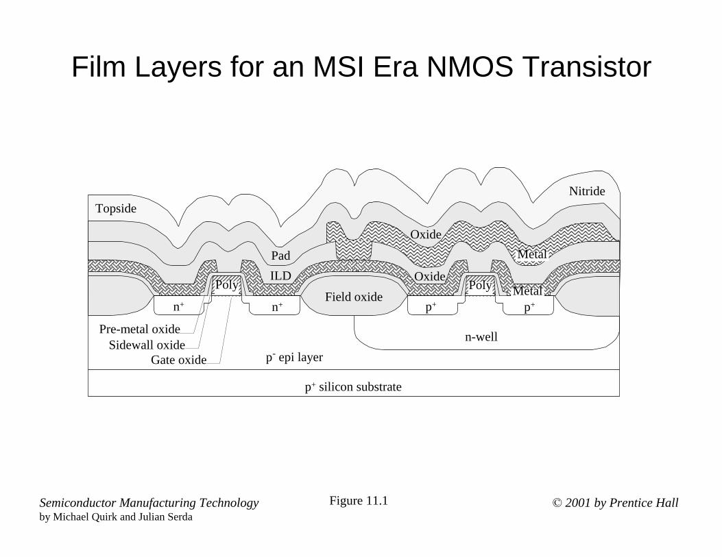
Film Layers for an MSI Era NMOS Transistor
p+ silicon substrate
p- epi layer
Field oxiden+ n+ p+ p+
n-well
ILD OxidePad
Oxide
NitrideTopside
Gate oxideSidewall oxide
Pre-metal oxide
Poly
Metal
Poly Metal
Figure 11.1

© 2001 by Prentice HallSemiconductor Manufacturing Technologyby Michael Quirk and Julian Serda
Process Flow in a Wafer Fab
Test/Sort Implant
Diffusion Etch
Polish
PhotoCompleted wafer
Locations where thin films are deposited
Unpatterned wafer
Wafer startThin Films
Wafer fabrication (front-end)
Used with permission of Advanced Micro Devices
Figure 11.2

© 2001 by Prentice HallSemiconductor Manufacturing Technologyby Michael Quirk and Julian Serda
Introduction
• Film Layering in Wafer Fab– Diffusion– Thin Films
• Film Layering Terminology• Multilayer Metallization
– Metal Layers– Dielectric Layers

© 2001 by Prentice HallSemiconductor Manufacturing Technologyby Michael Quirk and Julian Serda
Multilevel Metallization on a ULSI Wafer
Figure 11.3
Passivation layer Bonding pad metal
p+ Silicon substrate
Via
ILD-2
ILD-3
ILD-4
ILD-5
M-1
M-2
M-3
M-4
p- Epitaxial layer
p+p+
ILD-6
LI oxide
STI
n-well p-well
ILD-1
Poly gate
n+ p+p+ p+p+ n+n+
LI metal

© 2001 by Prentice HallSemiconductor Manufacturing Technologyby Michael Quirk and Julian Serda
Metal Layers in a Chip
Micrograph courtesy of Integrated Circuit Engineering
Photo 11.1

© 2001 by Prentice HallSemiconductor Manufacturing Technologyby Michael Quirk and Julian Serda
Film Deposition
Thin Film Characteristics• Good step coverage
• Ability to fill high aspect ratio gaps (conformality)
• Good thickness uniformity
• High purity and density
• Controlled stoichiometries
• High degree of structural perfection with low film stress
• Good electrical properties
• Excellent adhesion to the substrate material and subsequent films

© 2001 by Prentice HallSemiconductor Manufacturing Technologyby Michael Quirk and Julian Serda
Solid Thin Film
Silicon substrate
Oxide
WidthLen
gth
Thickness
Thin films are very thin in comparison to the substrate.
Figure 11.4

© 2001 by Prentice HallSemiconductor Manufacturing Technologyby Michael Quirk and Julian Serda
Film Coverage over Steps
Conformal step coverage Nonconformal step coverage
Uniform thickness
Figure 11.5

© 2001 by Prentice HallSemiconductor Manufacturing Technologyby Michael Quirk and Julian Serda
Aspect Ratio for Film Deposition
Aspect Ratio = Depth Width
=2 1
Aspect Ratio = 500 Å250 Å
500 Å
D
250 ÅW
Figure 11.6

© 2001 by Prentice HallSemiconductor Manufacturing Technologyby Michael Quirk and Julian Serda
High Aspect Ratio Gap
Photograph courtesy of Integrated Circuit Engineering
Photo 11.2

© 2001 by Prentice HallSemiconductor Manufacturing Technologyby Michael Quirk and Julian Serda
Stages of Film Growth
Continuous film
Gas molecules
Nucleation Coalescence
Substrate
Figure 11.7

© 2001 by Prentice HallSemiconductor Manufacturing Technologyby Michael Quirk and Julian Serda
Chemical Processes Physical Processes
Chemical VaporDeposition (CVD) Plating
Physical VaporDeposition
(PVD orSputtering)
Evaporation Spin OnMethods
Atmospheric PressureCVD (APCVD) or
Sub-Atmospheric CVD(SACVD)
Electrochemicaldeposition (ECD),
commonly referred toas electroplating
DC Diode Filament andElectron Beam
Spin onglass (SOG)
Low Pressure CVD(LPCVD) Electroless Plating Radio Frequency
(RF)Molecular BeamEpitaxy (MBE)
Spin ondielectric
(SOD)Plasma Assisted CVD:§ Plasma Enhanced
CVD (PECVD)§ High Density
Plasma CVD(HDPCVD)
DC Magnetron
Vapor Phase Epitaxy(VPE) and
Metal-organic CVD(MOCVD)
Ionized metalplasma (IMP)
Dielectrics: Chapter 11Metals: Chapter 12 Chapter 12 Chapter 12 Chapter 12 Chapter 11
Techniques of Film Deposition13
Table 11.1

© 2001 by Prentice HallSemiconductor Manufacturing Technologyby Michael Quirk and Julian Serda
Chemical Vapor Deposition
The Essential Aspects of CVD1. Chemical action is involved, either through chemical
reaction or by thermal decomposition (referred to as pyrolysis).
2. All material for the thin film is supplied by an external source.
3. The reactants in a CVD process must start out in the vapor phase (as a gas).

© 2001 by Prentice HallSemiconductor Manufacturing Technologyby Michael Quirk and Julian Serda
Chemical Vapor Deposition Tool
Photograph courtesy of Novellus, Sequel CVD
Photo 11.3

© 2001 by Prentice HallSemiconductor Manufacturing Technologyby Michael Quirk and Julian Serda
CVD Reaction
• CVD Reaction Steps• Rate Limiting Step• CVD Gas Flow Dynamics• Pressure in CVD• Doping During CVD
– PSG– BSG– FSG

© 2001 by Prentice HallSemiconductor Manufacturing Technologyby Michael Quirk and Julian Serda
Schematic of CVD Transport and Reaction Steps
CVD Reactor
Substrate
Continuous film
8) By-product removal
1) Mass transport of reactants
By-products2) Film precursor
reactions
3) Diffusion of gas molecules
4) Adsorption of precursors
5) Precursor diffusion into substrate 6) Surface reactions
7) Desorption of byproducts
Exhaust
Gas delivery
Figure 11.8

© 2001 by Prentice HallSemiconductor Manufacturing Technologyby Michael Quirk and Julian Serda
Gas Flow in CVD
Gas flow
Deposited film
Silicon substrate
Reaction product
Diffusion of reactants
Figure 11.9
© 2001 by Prentice HallSemiconductor Manufacturing Technologyby Michael Quirk and Julian Serda
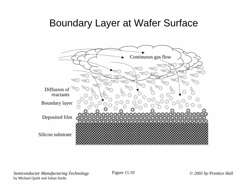
Figure 11.10
Boundary Layer at Wafer Surface
Continuous gas flow
Deposited film
Silicon substrate
Boundary layer
Diffusion of reactants

© 2001 by Prentice HallSemiconductor Manufacturing Technologyby Michael Quirk and Julian Serda
CVD Deposition Systems
• CVD Equipment Design– CVD reactor heating– CVD reactor configuration– CVD reactor summary
• Atmospheric Pressure CVD, APCVD • Low Pressure CVD, LPCVD• Plasma-Assisted CVD• Plasma-Enhanced CVD, PECVD• High-Density Plasma CVD, HDPCVD

© 2001 by Prentice HallSemiconductor Manufacturing Technologyby Michael Quirk and Julian Serda
CVD Reactor Types
CVD Reactor Types Atmospheric Low-pressure Batch Single-waferHot-wall √ √ √Cold-wall √ √ √ √Continuous motion √ √Epitaxial √ √Plenum √ √Nozzle √ √Barrel √ √Cold-wall planar √ √ √Plasma-assisted √ √ √Vertical-flow Isothermal √ √ √
Figure 11.11

© 2001 by Prentice HallSemiconductor Manufacturing Technologyby Michael Quirk and Julian Serda
Types of CVD Reactors and Principal Characteristics
Process Advantages Disadvantages Applications
APCVD(Atmospheric PressureCVD)
Simple reactor, fastdeposition, lowtemperature.
Poor step coverage,particle contamination,and low throughput.
Low-temperature oxides(both doped and undoped).
LPCVD(Low Pressure CVD)
Excellent purity anduniformity, conformalstep coverage, large wafercapacity.
High temperature, lowdeposition rate, moremaintenance intensiveand requires vacuumsystem.
High-temperature oxides(both doped and undoped),silicon nitride, polysilicon,W, WSi2.
Plasma Assisted CVD:§ Plasma Enhanced
CVD (PECVD)§ High Density Plasma
CVD (HDPCVD)
Low temperature, fastdeposition, good stepcoverage, good gap fill.
Requires RF system,higher cost, stress ismuch higher with atensile component, andchemical (e.g., H2) andparticle contamination.
High aspect ratio gap fill,low-temperature oxides overmetals, ILD-1, ILD, copperseed layer for dualdamascene, passivation(nitride).
Table 11.2

© 2001 by Prentice HallSemiconductor Manufacturing Technologyby Michael Quirk and Julian Serda
Continuous-Processing APCVD Reactors
WaferFilmReactant gas 2
Reactant gas 1
Inert separator gas
(a) Gas-injection type
N2
Reactant gases
Heater
N2 N2 N2N2 N2
Wafer
(b) Plenum typeFigure 11.12

© 2001 by Prentice HallSemiconductor Manufacturing Technologyby Michael Quirk and Julian Serda
Excellent Step Coverage of APCVD TEOS-O3
Liner oxide
p Silicon substrate
p Epitaxial layer
n-well p-well
Trench CVD oxide
TEOS-O3
Trench fill by chemical vapor deposition
Nitride
-
+
Figure 11.3

© 2001 by Prentice HallSemiconductor Manufacturing Technologyby Michael Quirk and Julian Serda
Planarized Surface after Reflow of PSG
After reflow
PSG
Before reflow
PSG
Metal or polysilicon
Figure 11.14

© 2001 by Prentice HallSemiconductor Manufacturing Technologyby Michael Quirk and Julian Serda
LPCVD Reaction Chamber for Deposition of Oxides, Nitrides, or Polysilicon
Three-zone heating element
Spike thermocouples (external, control)
Pressure gauge
Exhaust tovacuum pump
Gas inletProfile thermocouples
(internal)
Figure 11.16

© 2001 by Prentice HallSemiconductor Manufacturing Technologyby Michael Quirk and Julian Serda
Oxide Deposition with TEOS LPCVD
Pressure controllerThree-
zone heater
Heater TEOSN2 O2 Vacuum
pump
Gas flow controller
LPCVDFurnace
Temp. controller
Computer terminal operator interface
Furnace microcontroller
Exhaust
Figure 11.17

© 2001 by Prentice HallSemiconductor Manufacturing Technologyby Michael Quirk and Julian Serda
Doped Polysilicon as a Gate electrode
n-well p-well
p- Epitaxial layer
p+ Silicon substrate
Polysilicon gate
p+ p+ p+n+n+n+
Figure 11.18

© 2001 by Prentice HallSemiconductor Manufacturing Technologyby Michael Quirk and Julian Serda
Advantages of Plasma Assisted CVD
1. Lower processing temperature (250 – 450°C).
2. Excellent gap-fill for high aspect ratio gaps (with high-density plasma).
3. Good film adhesion to the wafer.
4. High deposition rates.
5. High film density due to low pinholes and voids.
6. Low film stress due to lower processing temperature.

© 2001 by Prentice HallSemiconductor Manufacturing Technologyby Michael Quirk and Julian Serda
Film Formation during Plasma-Based CVD
PECVD reactor
Continuous film
8) By-product removal
1) Reactants enter chamber
Substrate
2) Dissociation of reactants by electric fields
3) Film precursors are formed
4) Adsorption of precursors
5) Precursor diffusion into substrate 6) Surface reactions
7) Desorption of by-products
Exhaust
Gas delivery
RF generator
By-products
Electrode
Electrode
RF field
Figure 11.19

© 2001 by Prentice HallSemiconductor Manufacturing Technologyby Michael Quirk and Julian Serda
General Schematic of PECVD for Deposition of Oxides, Nitrides, Silicon Oxynitride or Tungsten
Process gases
Gas flow controller
Pressure controller
Roughingpump
Turbopump
Gas panel
RF generatorMatching network
Microcontroller operator Interface
Exhaust
Gas dispersion screen
Electrodes
Figure 11.20

© 2001 by Prentice HallSemiconductor Manufacturing Technologyby Michael Quirk and Julian Serda
Property LPCVD PECVD
Deposition temperature (°C) 700 – 800 300 – 400
Composition Si3N4 SixNyHz
Step coverage Fair Conformal
Stress at 23°C on silicon(dyn/cm-2)
1.2 – 1.8 x 10¹⁰
(tensile)1 – 8 x 10⁹
(tensile or compressive)
Properties of Silicon Nitride for LPCVD Versus PECVD
Table 11.3

© 2001 by Prentice HallSemiconductor Manufacturing Technologyby Michael Quirk and Julian Serda
High Density Plasma Deposition Chamber
Photograph courtesy of Applied Materials, Ultima HDPCVD Centura
Photo 11.4
• Popular in mid-1990s• High density plasma• Highly directional due to
wafer bias• Fills high aspect ratio
gaps• Backside He cooling to
relieve high thermal load• Simultaneously deposits
and etches film to prevent bread-loaf and key-hole effects

© 2001 by Prentice HallSemiconductor Manufacturing Technologyby Michael Quirk and Julian Serda
Five Steps of HDPCVD Process
1. Ion-induced deposition
2. Sputter etch
3. Redeposition
4. Hot neutral CVD
5. Reflection

© 2001 by Prentice HallSemiconductor Manufacturing Technologyby Michael Quirk and Julian Serda
Figure 11.22
Dep-Etch-Dep Process
Film deposited with PECVD creates pinch-off at the entrance to a gap resulting in a void in the gap fill.
Key-hole defect
Bread-loaf effect
Metal
SiO2
The solution begins here
1) Ion-induced deposition of film precursors
2) Argon ions sputter-etch excess film at gap entrance resulting in a beveled appearance in the film.
3) Etched material is redeposited. The process is repeated resulting in an equal “bottom-up” profile.
Cap

© 2001 by Prentice HallSemiconductor Manufacturing Technologyby Michael Quirk and Julian Serda
3-Part Process for Dielectric Gap Fill
2) PECVD cap
Cap
1) HDPCVD gap fill
SiO2
Aluminum
3) Chemical mechanical planarization

© 2001 by Prentice HallSemiconductor Manufacturing Technologyby Michael Quirk and Julian Serda
Effects of Keyholes in ILD on Metal Step Coverage
b) SiO2 is planarized
c) Next layer of aluminum is deposited
Metal void caused by keyhole defect in SiO2
a) SiO2 deposited by PECVDSiO2
Keyhole defect in interlayer dielectric
Aluminum
© 2001 by Prentice HallSemiconductor Manufacturing Technologyby Michael Quirk and Julian Serda
Dielectrics and Performance
• Dielectric Constant• Gap Fill• Chip Performance• Low-k Dielectric• High-k Dielectric• Device Isolation
– LOCOS– STI

© 2001 by Prentice HallSemiconductor Manufacturing Technologyby Michael Quirk and Julian Serda
Potential low-kDielectric
DielectricConstant
(k)
Gap Fill(µm)
CureTemp.(°C)
Remarks
FSG (siliconoxyfluoride, SiXOFy)
3.4 – 4.1 <0.35 No issueFSG has almost the same k-value as SiO2 andreliability concern that fluorine will attack andcorrode tantalum barrier metal.
HSQ (hydrogensilsesquioxane) 2.9 <0.10 350 – 450
Silicon-based resin polymer available insolution as Fox (Flowable Oxide) for spin-oncoating application. May require surfacepassivation to reduce moisture absorption.Cure is done in nitrogen.
Nanoporous silica 1.3 – 2.5 <0.25 400
Inorganic material with tunable dielectricconstant that relies on pore density. Increasedporosity reduces mechanical integrity –porous material must withstand polishing,etching and heat treatments withoutdegradation.
Poly(arylene) ether(PAE) 2.6 – 2.8 <0.15 375 – 425 Spin-on aromatic polymer with excellent
adhesion and ability to be polished with CMP.
a-CF (fluorinatedamorphous carbon orFLAC)1
2.8 <0.18 250 – 350
Leading candidate for CVD deposition withhigh density plasma CVD (HDPCVD) toproduce film with good thermal stability andadhesion.
Parylene AF4 (aliphatictetrafluorinated poly-p-xylylene)
2.5 <0.18 420 – 450
CVD film that meets adhesion and viaresistance requirements with need to maintaingas delivery system at 200°C to controlparylene precursor flow rate.
1 P. Singer, Technology News: Wafer Processing, Semiconductor International, October, 1998, p. 44.
Potential Low-k Materials for ILD of ULSI Interconnects
Table 11.4
© 2001 by Prentice HallSemiconductor Manufacturing Technologyby Michael Quirk and Julian Serda
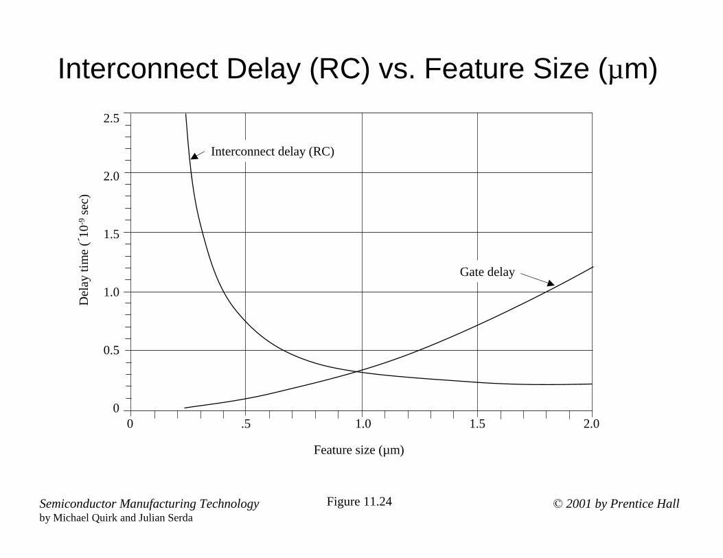
Interconnect Delay (RC) vs. Feature Size (µm)
Figure 11.24
2.5
2.0
1.5
1.0
0.5
00 .5 1.0 1.5 2.0
Feature size (µm)
Del
ay ti
me
(´10-9
sec)
Interconnect delay (RC)
Gate delay

© 2001 by Prentice HallSemiconductor Manufacturing Technologyby Michael Quirk and Julian Serda
Total Interconnect Wiring Capacitance
Cap
acita
nce
(10-1
2Fa
rads
/cm
)
7
6
5
4
3
2
1
00 0.5 1.0 1.5 2.0 2.5 3.0
Space (µm)
K = 4
K = 3
K = 2
K= 1
Redrawn with permission from Semiconductor International, September 1998
Figure 11.25

© 2001 by Prentice HallSemiconductor Manufacturing Technologyby Michael Quirk and Julian Serda
Electrical Mechanical Thermal Chemical Processing Metallization
Low dielectricconstant Good adhesion Thermal
stabilityResistant: acids
and bases Patternability Low contactresistance
Low dielectricloss Low shrinkage
Low coefficientof thermalexpansion
Etch selectivity Good gap fillLow
electromigration(corrosion)
Low leakage Crack resistant Highconductivity Low impurities Planarization Low stress
voiding
High reliability Low stress No corrosion Low pin hole Hillock (smoothsurface)
Good hardness Low moistureuptake Low particulate
Compatible withbarrier metals (Ta,
TaN, TiN, etc.)
Storage life
Low-k Dielectric Film Requirements
Table 11.5

© 2001 by Prentice HallSemiconductor Manufacturing Technologyby Michael Quirk and Julian Serda
General Diagram of DRAM Stacked Capacitors
SiO2 dielectric
Doped polysiliconcapacitor plate
Doped polysiliconcapacitor plate
Buried contactdiffusion
SiO2 dielectric Doped polysiliconcapacitor plate
Doped polysiliconcapacitor plate
Buried contactdiffusion
Figure 11.26

© 2001 by Prentice HallSemiconductor Manufacturing Technologyby Michael Quirk and Julian Serda
Shallow Trench Isolation
Photograph courtesy of Integrated Circuit Engineering
Photo 11.5

© 2001 by Prentice HallSemiconductor Manufacturing Technologyby Michael Quirk and Julian Serda
Spin-on Dielectrics
• Spin-on Glass (SOG)• Spin-on Dielectric (SOD)• Epitaxy
– Epitaxy growth methods• Vapor-phase epitaxy• Metalorganic CVD• Molecular-beam epitaxy

© 2001 by Prentice HallSemiconductor Manufacturing Technologyby Michael Quirk and Julian Serda
Gap-Fill with Spin-On-Glass (SOG)
2) SOG after curing1) Initial SOG gap fill 3) CVD oxide cap
Cap
Figure 11.27

© 2001 by Prentice HallSemiconductor Manufacturing Technologyby Michael Quirk and Julian Serda
Major Operation Process Step Parameter
Apply bowl speed 50 rpm
Maximum bowl speed 800 – 1500 rpm
Backside rinse 800 rpm, 5 sec
Topside edge bead removal 1000 rpm, 10 sec
Spin coating
Spin Dry 1000 rpm, 5 sec
Initial soft-bake cure 200°C, 60 sec, N2 purgeCure
In-line cure 475°C, 60 sec, N2 ambient
Proposed HSQ Low-k Dielectric Processing Parameters
Table 11.6

© 2001 by Prentice HallSemiconductor Manufacturing Technologyby Michael Quirk and Julian Serda
Epitaxy
• Epitaxy Growth Model• Epitaxy Growth Methods
– Vapor-Phase Epitaxy (VPE)– Metalorganic CVD (MOCVD)– Molecular-Beam Epitaxy (MBE)

© 2001 by Prentice HallSemiconductor Manufacturing Technologyby Michael Quirk and Julian Serda
Silicon Epitaxial Growth on a Silicon Wafer
Si
Si
ClCl
HH
Si
Si
Si Si
Si Si
Si
Si
Si
Si
Si
ClH
Cl
H
Chemical reaction
By-products
Deposited siliconEpitaxial layer
Single silicon substrate
Figure 11.28