Semiconductor Manufacturing Technologyjupiter.math.nctu.edu.tw/~weng/courses/IC_2007/... ·...
40
© 2001 by Prentice Hall Semiconductor Manufacturing Technology by Michael Quirk and Julian Serda Semiconductor Manufacturing Technology Michael Quirk & Julian Serda © October 2001 by Prentice Hall Chapter 10 Oxidation Semiconductor Manufacturing Technology Michael Quirk & Julian Serda © October 2001 by Prentice Hall Chapter 10 Oxidation © 2000 by Prentice Hall Semiconductor Manufacturing Technology by Michael Quirk and Julian Serda
Transcript of Semiconductor Manufacturing Technologyjupiter.math.nctu.edu.tw/~weng/courses/IC_2007/... ·...
© 2001 by Prentice HallSemiconductor Manufacturing Technologyby Michael Quirk and Julian Serda
Semiconductor Manufacturing Technology
Michael Quirk & Julian Serda© October 2001 by Prentice Hall
Chapter 10
Oxidation
Semiconductor Manufacturing Technology
Michael Quirk & Julian Serda© October 2001 by Prentice Hall
Chapter 10
Oxidation
© 2000 by Prentice HallSemiconductor Manufacturing Technologyby Michael Quirk and Julian Serda
© 2001 by Prentice HallSemiconductor Manufacturing Technologyby Michael Quirk and Julian Serda
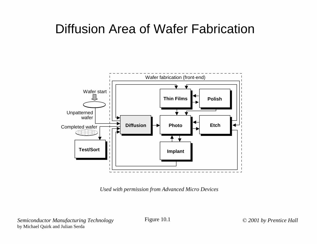
Diffusion Area of Wafer Fabrication
Test/Sort
Thin Films
Implant
Diffusion Etch
Polish
PhotoCompleted wafer
Wafer fabrication (front-end)
Unpatternedwafer
Wafer start
Used with permission from Advanced Micro Devices
Figure 10.1
© 2001 by Prentice HallSemiconductor Manufacturing Technologyby Michael Quirk and Julian Serda
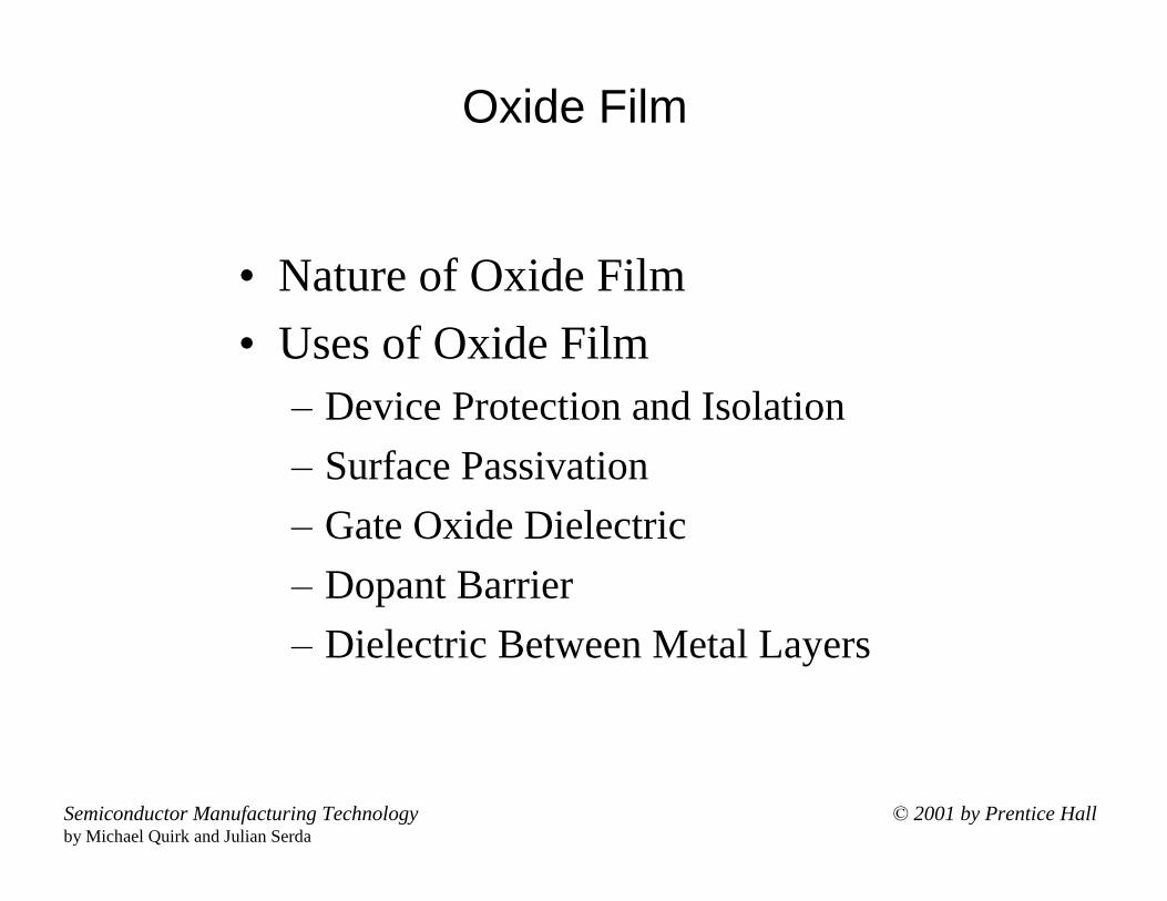
Oxide Film
• Nature of Oxide Film• Uses of Oxide Film
– Device Protection and Isolation– Surface Passivation– Gate Oxide Dielectric– Dopant Barrier– Dielectric Between Metal Layers
© 2001 by Prentice HallSemiconductor Manufacturing Technologyby Michael Quirk and Julian Serda
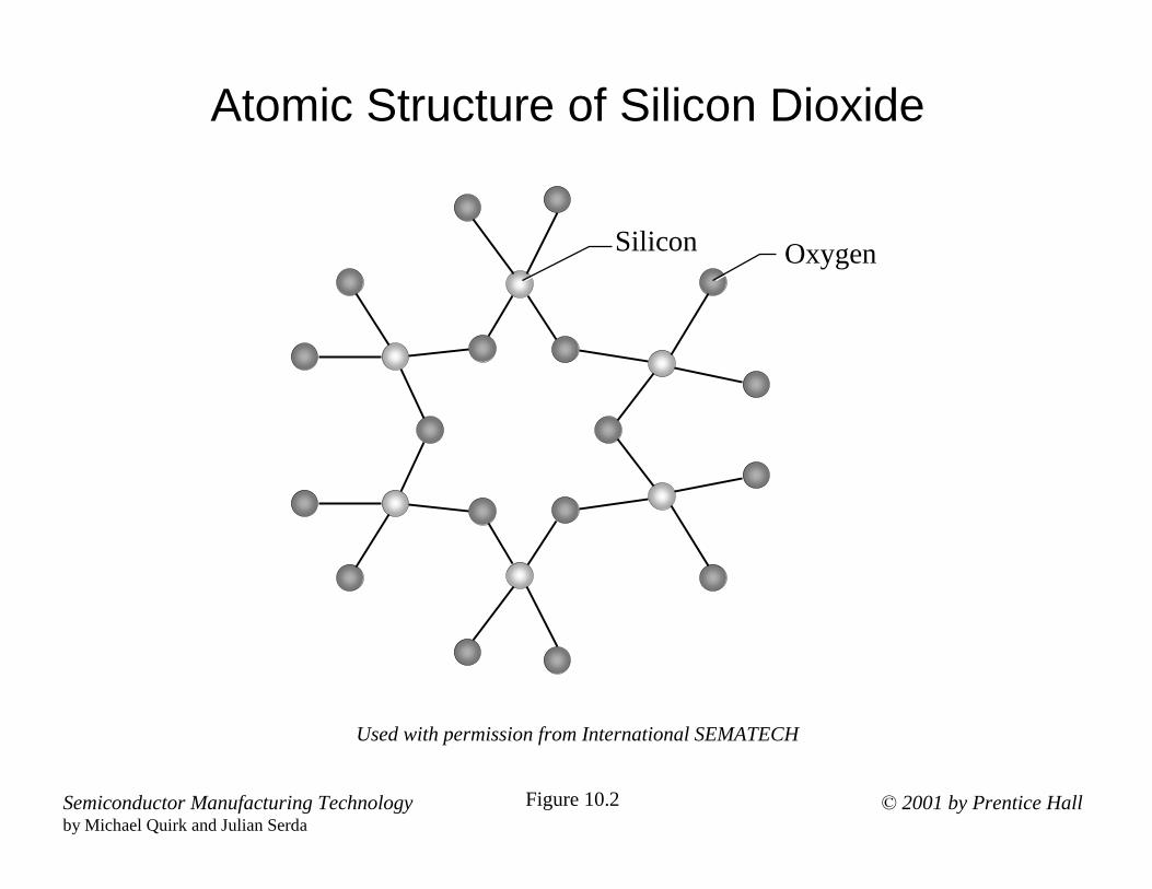
Atomic Structure of Silicon Dioxide
Silicon Oxygen
Used with permission from International SEMATECH
Figure 10.2

© 2001 by Prentice HallSemiconductor Manufacturing Technologyby Michael Quirk and Julian Serda
Table 10.1Oxide Applications: Native Oxide
Purpose: This oxide is a contaminant and generally undesirable. Sometimes used in memory storage or film passivation.
Comments: Growth rate at room temperature is 15 per hour up to about 40 Å.
p+ Silicon substrate
Silicon dioxide (oxide)
Table 10.1A

© 2001 by Prentice HallSemiconductor Manufacturing Technologyby Michael Quirk and Julian Serda
Table 10.1Oxide Applications: Field Oxide
Purpose: Serves as an isolation barrier between individual transistors to isolate them from each other.
Comments: Common field oxide thickness range from 2,500 Åto 15,000 Å. Wet oxidation is the preferred method.
Field oxide
Transistor site
p+ Silicon substrate
Table 10.1B

© 2001 by Prentice HallSemiconductor Manufacturing Technologyby Michael Quirk and Julian Serda
Table 10.1Oxide Applications: Gate Oxide
Purpose: Serves as a dielectric between the gate and source-drain parts of MOS transistor.
Comments: Growth rate at room temperature is 15 Å per hour up to about 40 Å. Common gate oxide film thickness range from about 30 Å to 500 Å. Dry oxidation is the preferred method.
Gate oxide
Transistor site
p+ Silicon substrate
Source Drain
Gate
Table 10.1C
© 2001 by Prentice HallSemiconductor Manufacturing Technologyby Michael Quirk and Julian Serda
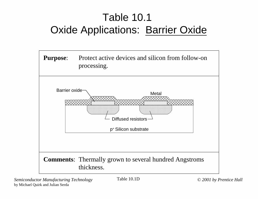
Table 10.1Oxide Applications: Barrier Oxide
Purpose: Protect active devices and silicon from follow-on processing.
Comments: Thermally grown to several hundred Angstroms thickness.
Barrier oxide
Diffused resistors
Metal
p+ Silicon substrate
Table 10.1D
© 2001 by Prentice HallSemiconductor Manufacturing Technologyby Michael Quirk and Julian Serda
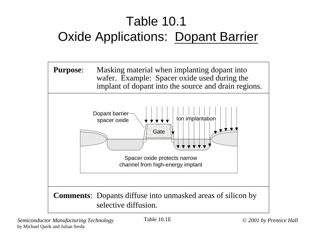
Table 10.1Oxide Applications: Dopant Barrier
Purpose: Masking material when implanting dopant into wafer. Example: Spacer oxide used during the implant of dopant into the source and drain regions.
Comments: Dopants diffuse into unmasked areas of silicon by selective diffusion.
Dopant barrierspacer oxide Ion implantation
Gate
Spacer oxide protects narrow channel from high-energy implant
Table 10.1E
© 2001 by Prentice HallSemiconductor Manufacturing Technologyby Michael Quirk and Julian Serda
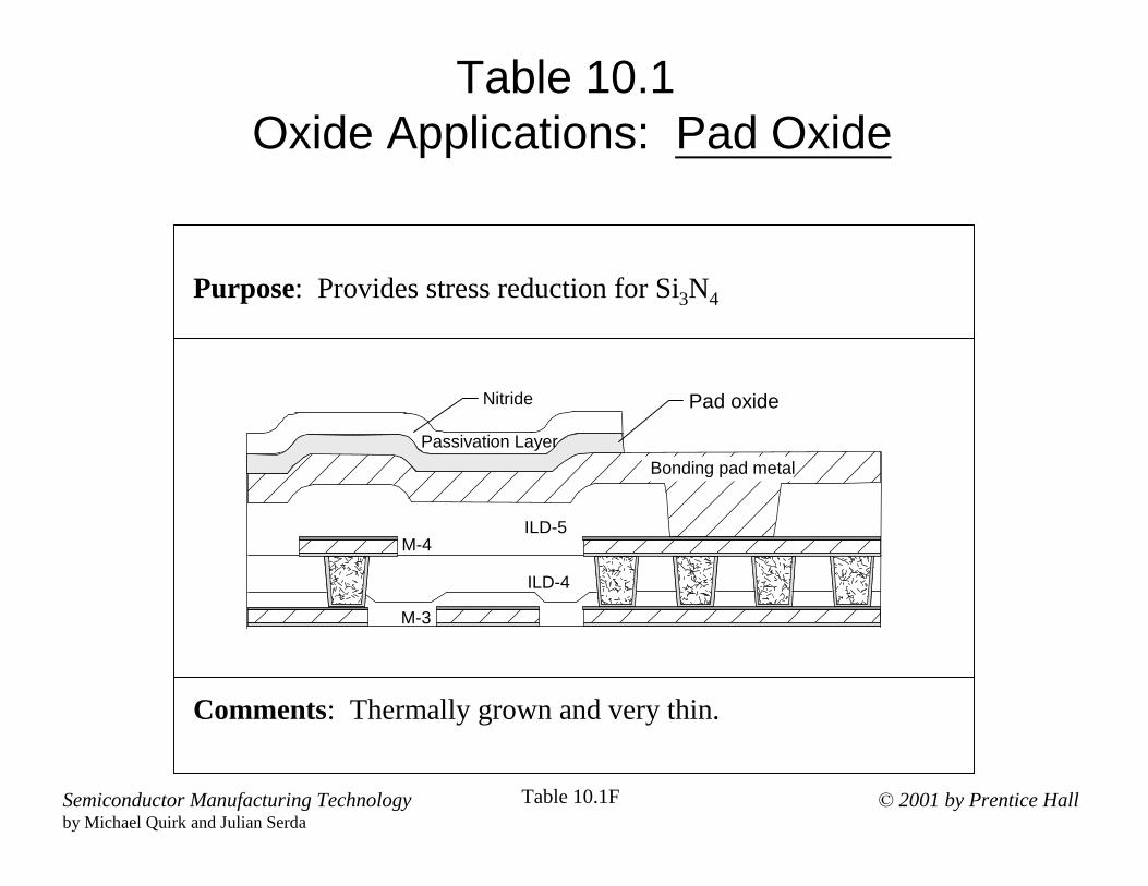
Table 10.1Oxide Applications: Pad Oxide
Purpose: Provides stress reduction for Si3N4
Comments: Thermally grown and very thin.
Passivation Layer
ILD-4
ILD-5
M-3
M-4
Pad oxide
Bonding pad metal
Nitride
Table 10.1F

© 2001 by Prentice HallSemiconductor Manufacturing Technologyby Michael Quirk and Julian Serda
Table 10.1Oxide Applications: Implant Screen Oxide
Purpose: Sometimes referred to as “sacrificial oxide”, screen oxide, is used to reduce implant channeling and damage. Assists creation of shallow junctions.
Comments: Thermally grown
Ion implantation Screen oxide
High damage to upper Sisurface + more channeling
Low damage to upper Sisurface + less channeling
p+ Silicon substrate
Table 10.1G
© 2001 by Prentice HallSemiconductor Manufacturing Technologyby Michael Quirk and Julian Serda
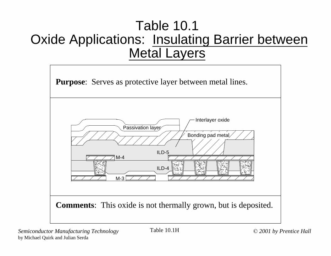
Passivation layer
ILD-4
ILD-5
M-3
M-4
Interlayer oxide
Bonding pad metal
Table 10.1Oxide Applications: Insulating Barrier between
Metal Layers
Purpose: Serves as protective layer between metal lines.
Comments: This oxide is not thermally grown, but is deposited.
Table 10.1H
© 2001 by Prentice HallSemiconductor Manufacturing Technologyby Michael Quirk and Julian Serda
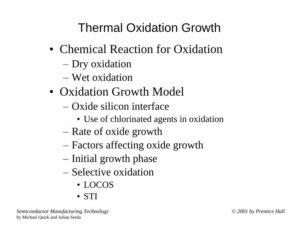
Thermal Oxidation Growth
• Chemical Reaction for Oxidation– Dry oxidation– Wet oxidation
• Oxidation Growth Model– Oxide silicon interface
• Use of chlorinated agents in oxidation– Rate of oxide growth– Factors affecting oxide growth– Initial growth phase– Selective oxidation
• LOCOS• STI
© 2001 by Prentice HallSemiconductor Manufacturing Technologyby Michael Quirk and Julian Serda
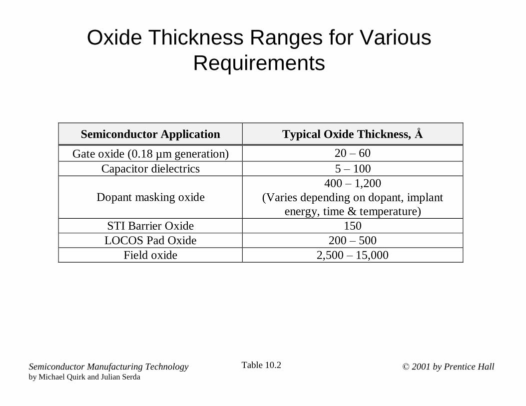
Oxide Thickness Ranges for Various Requirements
Semiconductor Application Typical Oxide Thickness, ÅGate oxide (0.18 µm generation) 20 – 60
Capacitor dielectrics 5 – 100
Dopant masking oxide400 – 1,200
(Varies depending on dopant, implantenergy, time & temperature)
STI Barrier Oxide 150LOCOS Pad Oxide 200 – 500
Field oxide 2,500 – 15,000
Table 10.2
© 2001 by Prentice HallSemiconductor Manufacturing Technologyby Michael Quirk and Julian Serda
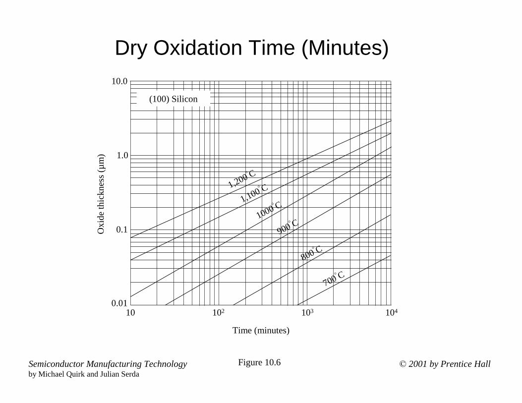
Dry Oxidation Time (Minutes)
Oxi
de th
ickn
ess (
µm)
(100) Silicon
Time (minutes)
10 104102 1030.01
0.1
1.0
10.0
700°C
800°C
900°C1000°C
1,100°C1,200°C
Figure 10.6
© 2001 by Prentice HallSemiconductor Manufacturing Technologyby Michael Quirk and Julian Serda
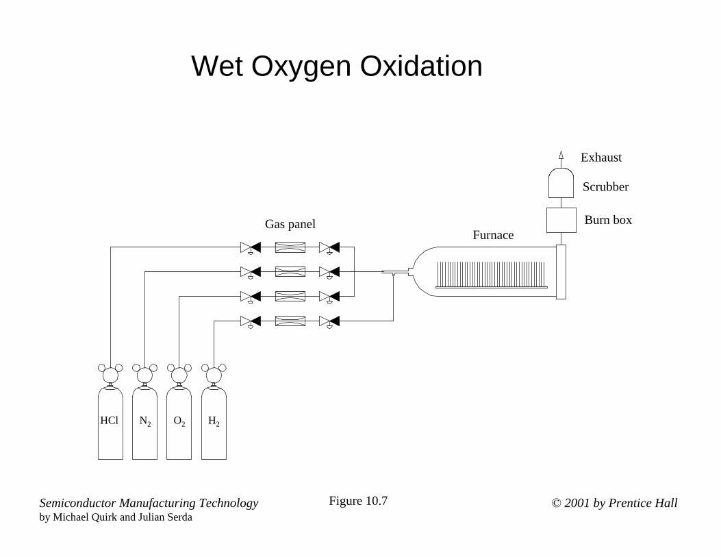
Wet Oxygen Oxidation
HCl N2 O2 H2
Gas panelFurnace
Burn box
Scrubber
Exhaust
Figure 10.7
© 2001 by Prentice HallSemiconductor Manufacturing Technologyby Michael Quirk and Julian Serda
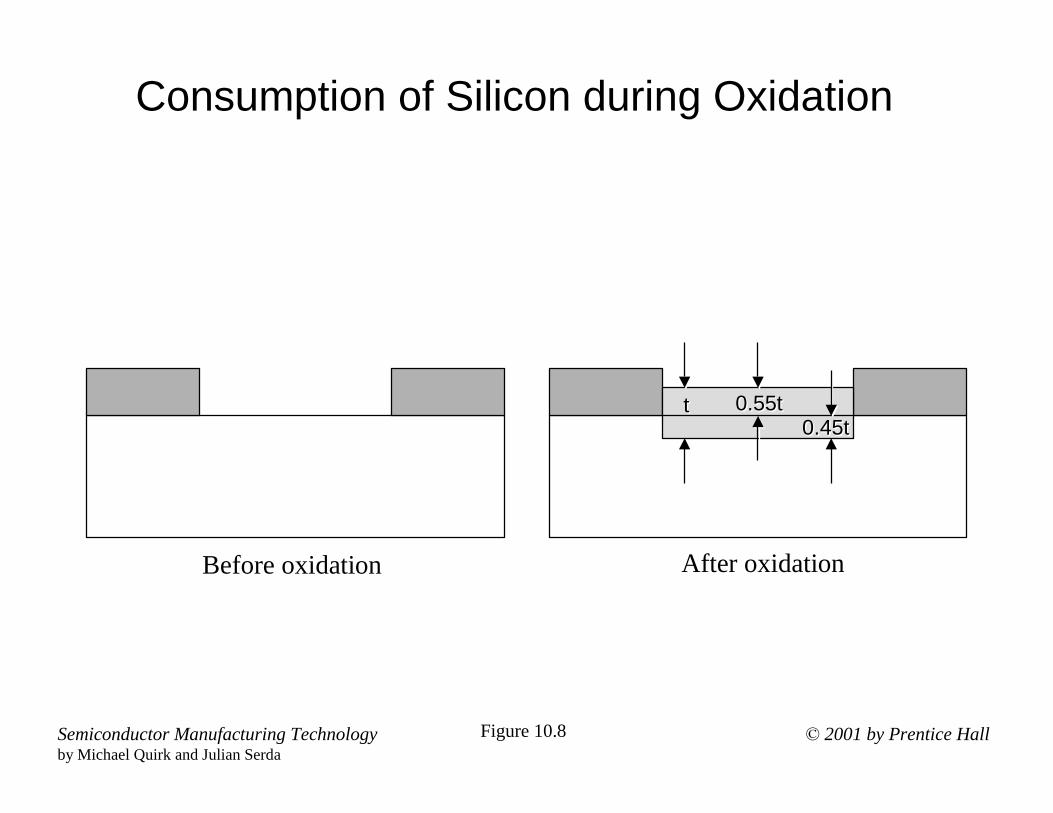
Consumption of Silicon during Oxidation
tt 0.55t0.55t0.45t0.45t
Before oxidation After oxidation
Figure 10.8
© 2001 by Prentice HallSemiconductor Manufacturing Technologyby Michael Quirk and Julian Serda
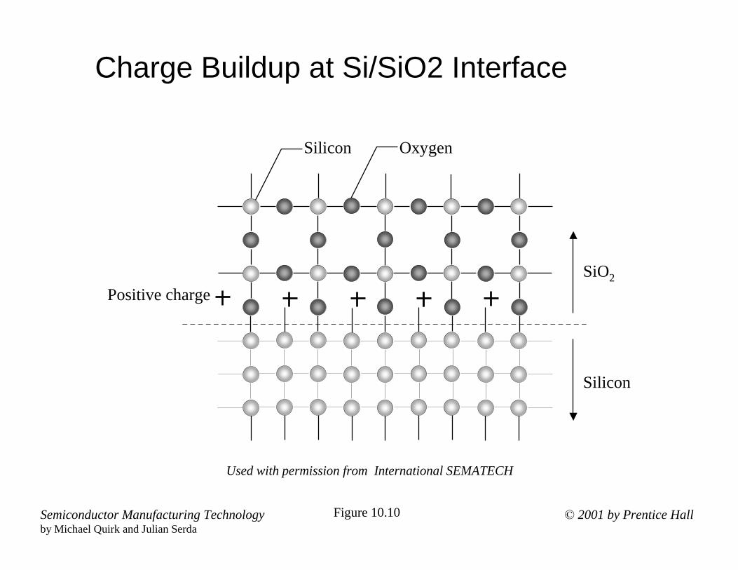
Charge Buildup at Si/SiO2 Interface
OxygenSilicon
Positive charge
Silicon
SiO2
Used with permission from International SEMATECH
Figure 10.10
© 2001 by Prentice HallSemiconductor Manufacturing Technologyby Michael Quirk and Julian Serda
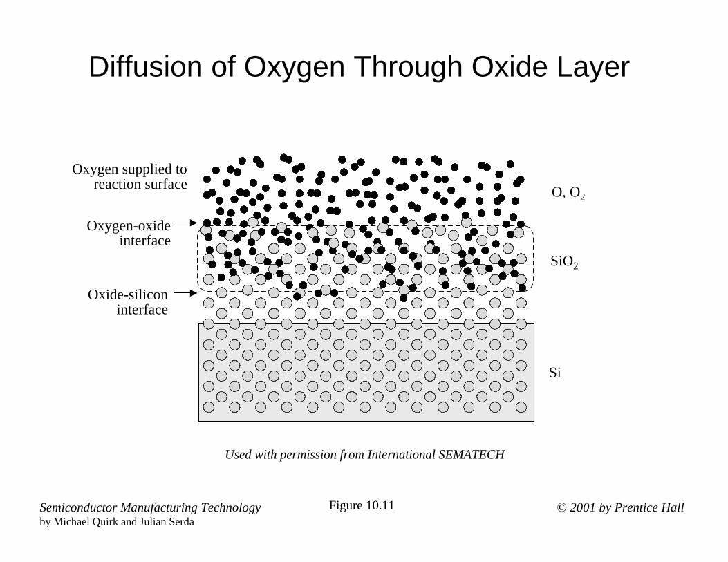
Diffusion of Oxygen Through Oxide Layer
Figure 10.11
Si
SiO2
O, O2
Oxide-silicon interface
Oxygen-oxide interface
Oxygen supplied to reaction surface
Used with permission from International SEMATECH
© 2001 by Prentice HallSemiconductor Manufacturing Technologyby Michael Quirk and Julian Serda
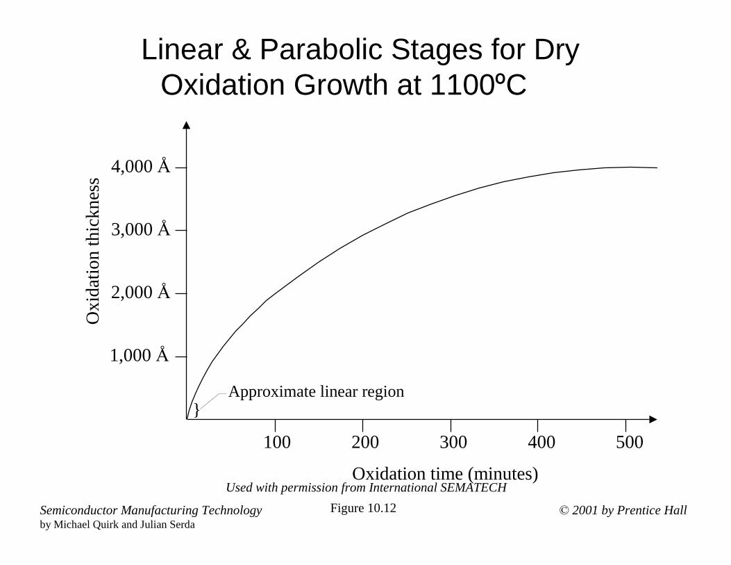
Linear & Parabolic Stages for Dry Oxidation Growth at 1100ºC
Used with permission from International SEMATECHFigure 10.12
}
100 200 300 400 500
Oxidation time (minutes)
4,000 Å
2,000 Å
3,000 Å
1,000 Å
Oxi
datio
n th
ickn
ess
Approximate linear region
© 2001 by Prentice HallSemiconductor Manufacturing Technologyby Michael Quirk and Julian Serda
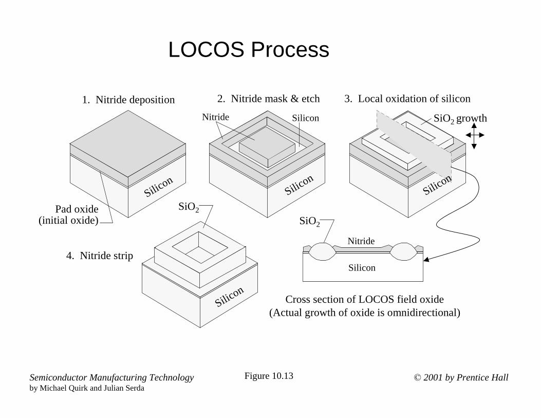
LOCOS Process
3. Local oxidation of silicon
Cross section of LOCOS field oxide(Actual growth of oxide is omnidirectional)
1. Nitride deposition
Pad oxide(initial oxide)
Silicon
2. Nitride mask & etch
Silicon
SiliconNitride SiO2 growth
Silicon
4. Nitride strip
Silicon
SiO2SiO2
Nitride
Silicon
Figure 10.13
© 2001 by Prentice HallSemiconductor Manufacturing Technologyby Michael Quirk and Julian Serda
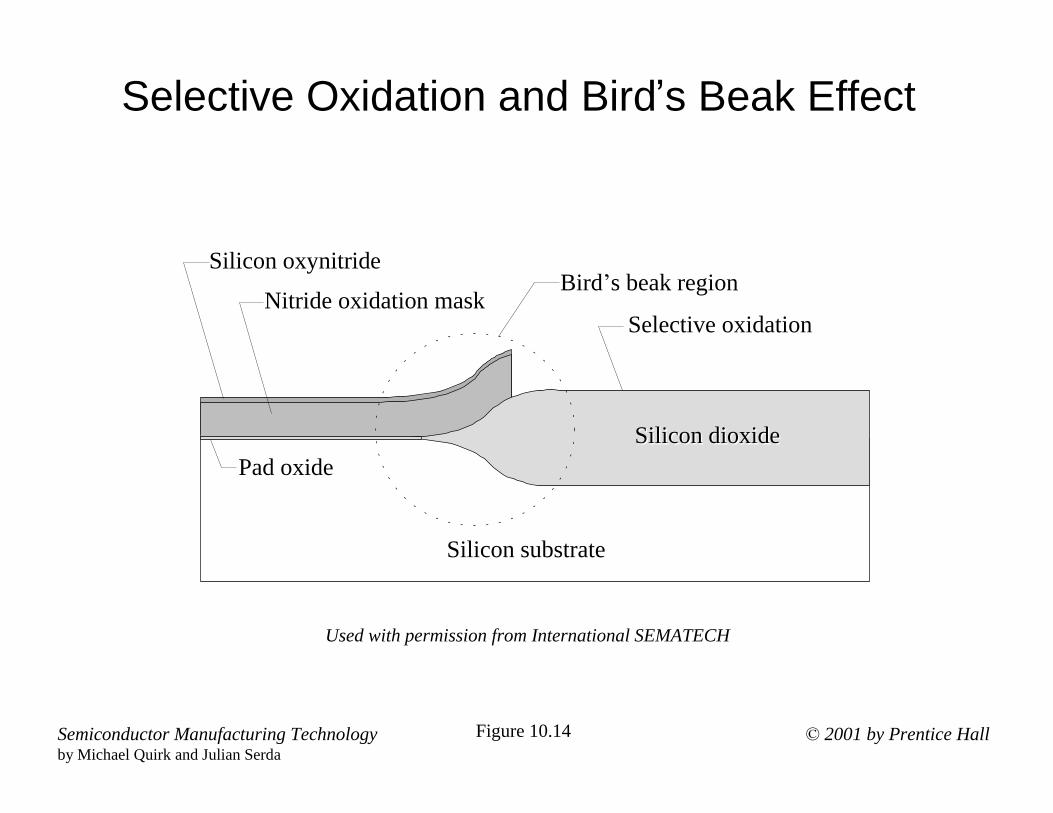
Selective Oxidation and Bird’s Beak Effect
Silicon oxynitride
Nitride oxidation maskBird’s beak region
Selective oxidation
Pad oxide
Silicon substrate
Silicon dioxideSilicon dioxide
Used with permission from International SEMATECH
Figure 10.14
© 2001 by Prentice HallSemiconductor Manufacturing Technologyby Michael Quirk and Julian Serda
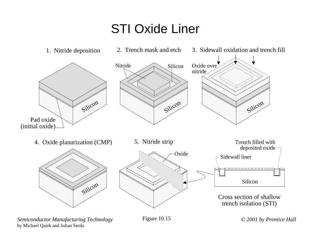
STI Oxide Liner
Cross section of shallow trench isolation (STI)
Silicon
Trench filled with deposited oxide
Sidewall liner
1. Nitride deposition
Pad oxide(initial oxide)
Silicon
2. Trench mask and etch
Silicon
SiliconNitride
4. Oxide planarization (CMP)
Silicon
5. Nitride strip
Oxide
3. Sidewall oxidation and trench fill
Oxide over nitride
Silicon
Figure 10.15
© 2001 by Prentice HallSemiconductor Manufacturing Technologyby Michael Quirk and Julian Serda
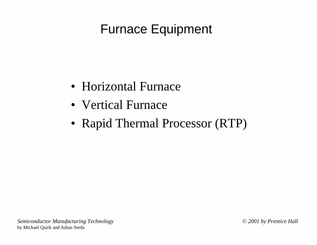
Furnace Equipment
• Horizontal Furnace• Vertical Furnace• Rapid Thermal Processor (RTP)
© 2001 by Prentice HallSemiconductor Manufacturing Technologyby Michael Quirk and Julian Serda
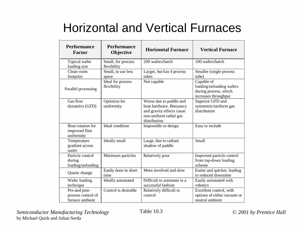
Horizontal and Vertical Furnaces
Table 10.3
PerformanceFactor
PerformanceObjective Horizontal Furnace Vertical Furnace
Typical waferloading size
Small, for processflexibility
200 wafers/batch 100 wafers/batch
Clean roomfootprint
Small, to use lessspace
Larger, but has 4 processtubes
Smaller (single processtube)
Parallel processing
Ideal for processflexibility
Not capable Capable ofloading/unloading wafersduring process, whichincreases throughput
Gas flowdynamics (GFD)
Optimize foruniformity
Worse due to paddle andboat hardware. Bouyancyand gravity effects causenon-uniform radial gasdistribution.
Superior GFD andsymmetric/uniform gasdistribution
Boat rotation forimproved filmuniformity
Ideal condition Impossible to design Easy to include
Temperaturegradient acrosswafer
Ideally small Large, due to radiantshadow of paddle
Small
Particle controlduringloading/unloading
Minimum particles Relatively poor Improved particle controlfrom top-down loadingscheme
Quartz change Easily done in shorttime
More involved and slow Easier and quicker, leadingto reduced downtime
Wafer loadingtechnique
Ideally automated Difficult to automate in asuccessful fashion
Easily automated withrobotics
Pre-and post-process control offurnace ambient
Control is desirable Relatively difficult tocontrol
Excellent control, withoptions of either vacuum orneutral ambient
© 2001 by Prentice HallSemiconductor Manufacturing Technologyby Michael Quirk and Julian Serda
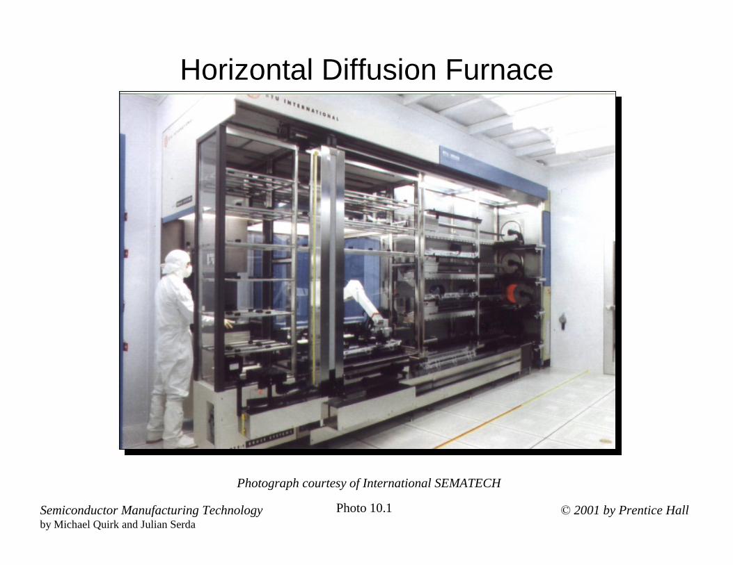
Horizontal Diffusion Furnace
Photograph courtesy of International SEMATECH
Photo 10.1
© 2001 by Prentice HallSemiconductor Manufacturing Technologyby Michael Quirk and Julian Serda
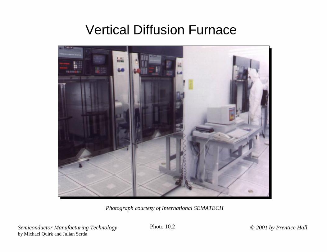
Vertical Diffusion Furnace
Photograph courtesy of International SEMATECH
Photo 10.2
© 2001 by Prentice HallSemiconductor Manufacturing Technologyby Michael Quirk and Julian Serda
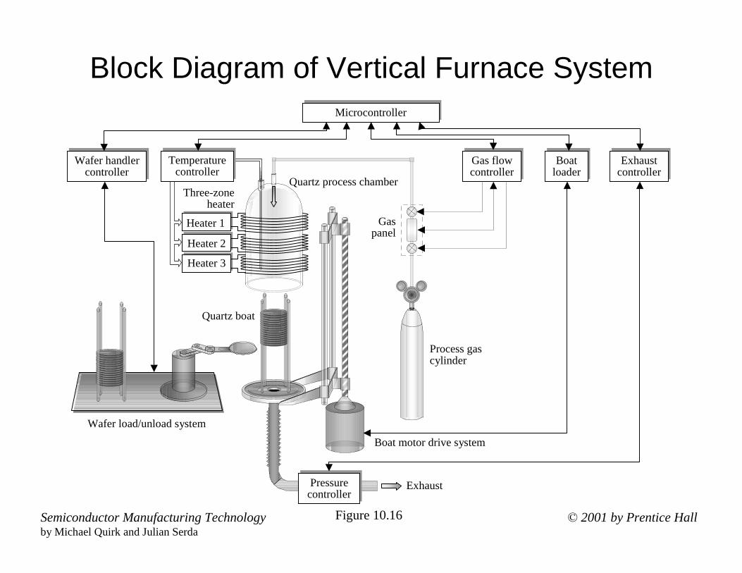
Block Diagram of Vertical Furnace System
Heater 1
Heater 2
Heater 3
PressurecontrollerPressure
controller
Gas flowcontrollerGas flowcontroller
Wafer handlercontroller
Wafer handlercontroller
BoatloaderBoat
loaderExhaust
controllerExhaust
controllerTemperature
controllerTemperature
controller
MicrocontrollerMicrocontroller
Wafer load/unload system
Boat motor drive system
Quartz boat
Quartz process chamberThree-zone
heaterGas
panel
Process gas cylinder
Exhaust
Figure 10.16
© 2001 by Prentice HallSemiconductor Manufacturing Technologyby Michael Quirk and Julian Serda
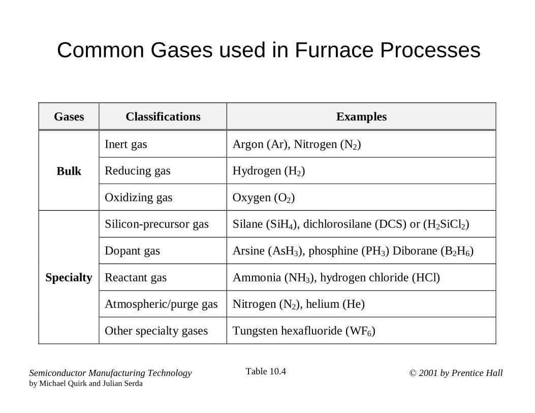
Common Gases used in Furnace Processes
Gases Classifications Examples
Inert gas Argon (Ar), Nitrogen (N2)
Reducing gas Hydrogen (H2)Bulk
Oxidizing gas Oxygen (O2)
Silicon-precursor gas Silane (SiH4), dichlorosilane (DCS) or (H2SiCl2)
Dopant gas Arsine (AsH3), phosphine (PH3) Diborane (B2H6)
Reactant gas Ammonia (NH3), hydrogen chloride (HCl)
Atmospheric/purge gas Nitrogen (N2), helium (He)
Specialty
Other specialty gases Tungsten hexafluoride (WF6)
Table 10.4
© 2001 by Prentice HallSemiconductor Manufacturing Technologyby Michael Quirk and Julian Serda
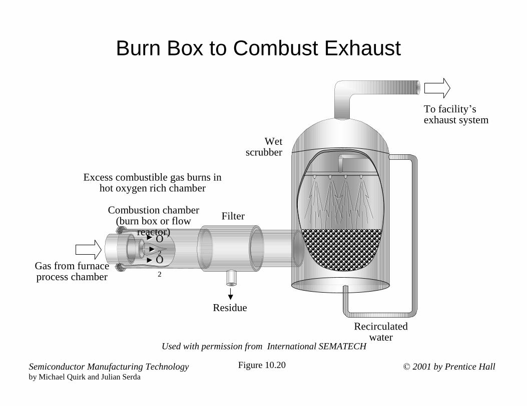
Burn Box to Combust Exhaust
OO22OO22
Combustion chamber (burn box or flow
reactor)Filter
Residue
Excess combustible gas burns in hot oxygen rich chamber
Gas from furnace process chamber
To facility’s exhaust system
Wet scrubber
Recirculatedwater
Used with permission from International SEMATECH
Figure 10.20

© 2001 by Prentice HallSemiconductor Manufacturing Technologyby Michael Quirk and Julian Serda
Thermal Profile of Conventional Versus Fast Ramp Vertical Furnace
Reprinted from the June 1996 edition of Solid State Technology, copyright 1996 by PennWell Publishing Company.
Figure 10.21
0 20 40 60 80 100 120 140 160 1800 20 40 60 80 100 120 140 160 180
1200
1000
800
600
400
1200
1000
800
600
400
Time (minutes) Time (minutes)
Tem
pera
ture
(°C
)
Tem
pera
ture
(°C
)
Fast RampConventional
© 2001 by Prentice HallSemiconductor Manufacturing Technologyby Michael Quirk and Julian Serda
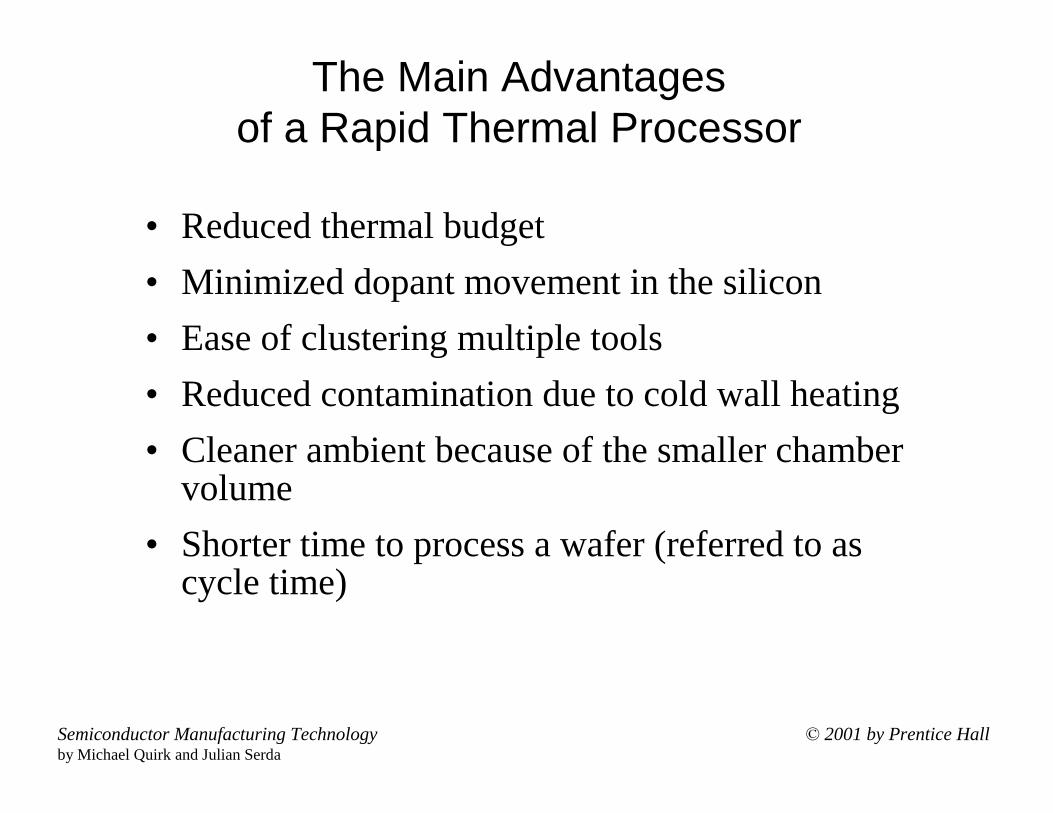
The Main Advantages of a Rapid Thermal Processor
• Reduced thermal budget• Minimized dopant movement in the silicon• Ease of clustering multiple tools• Reduced contamination due to cold wall heating• Cleaner ambient because of the smaller chamber
volume• Shorter time to process a wafer (referred to as
cycle time)

© 2001 by Prentice HallSemiconductor Manufacturing Technologyby Michael Quirk and Julian Serda
Comparison of Conventional Vertical Furnace and RTP
Vertical Furnace RTP
Batch Single-waferHot wall Cold wallLong time to heat and cool batch Short time to heat and cool waferSmall thermal gradient across wafer Large thermal gradient across waferLong cycle time Short cycle timeAmbient temperature measurement Wafer temperature measurementIssues: Issues: Large thermal budget Temperature uniformity Particles Minimize dopant movement Ambient control Repeatability from wafer to wafer
Throughput Wafer stress due to rapid heating Absolute temperature measurement
Table 10.5
© 2001 by Prentice HallSemiconductor Manufacturing Technologyby Michael Quirk and Julian Serda
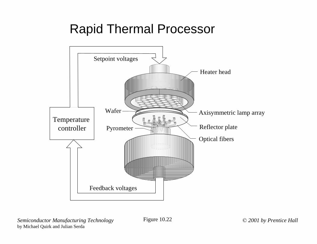
Rapid Thermal Processor
Temperature controller
Axisymmetric lamp arrayWafer
Reflector plate
Optical fibers
Pyrometer
Heater head
Feedback voltages
Setpoint voltages
Figure 10.22
© 2001 by Prentice HallSemiconductor Manufacturing Technologyby Michael Quirk and Julian Serda
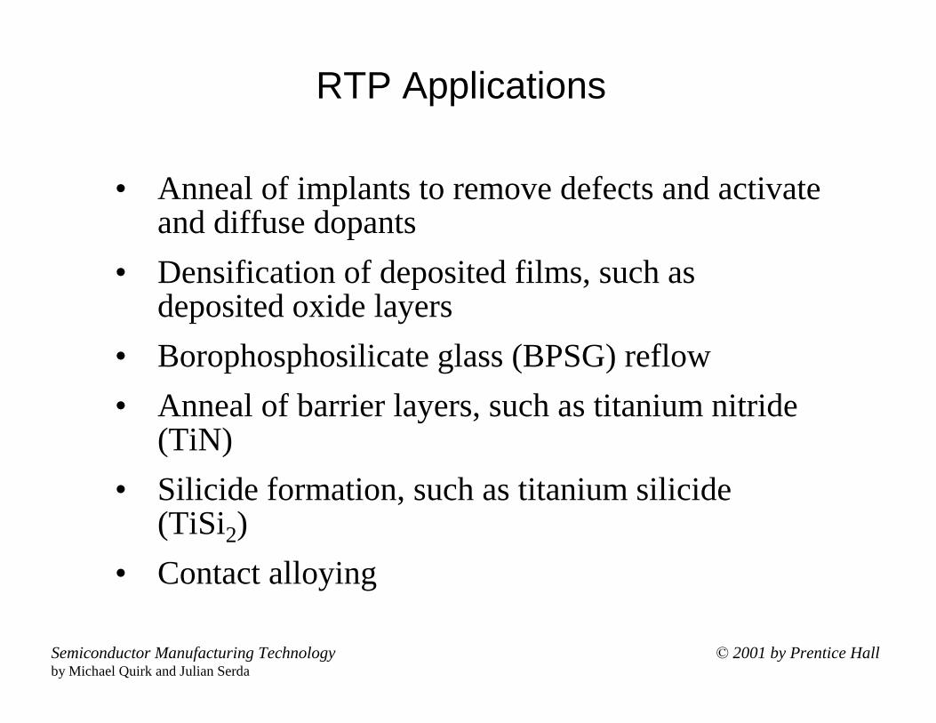
RTP Applications
• Anneal of implants to remove defects and activate and diffuse dopants
• Densification of deposited films, such as deposited oxide layers
• Borophosphosilicate glass (BPSG) reflow • Anneal of barrier layers, such as titanium nitride
(TiN)• Silicide formation, such as titanium silicide
(TiSi2)• Contact alloying
© 2001 by Prentice HallSemiconductor Manufacturing Technologyby Michael Quirk and Julian Serda
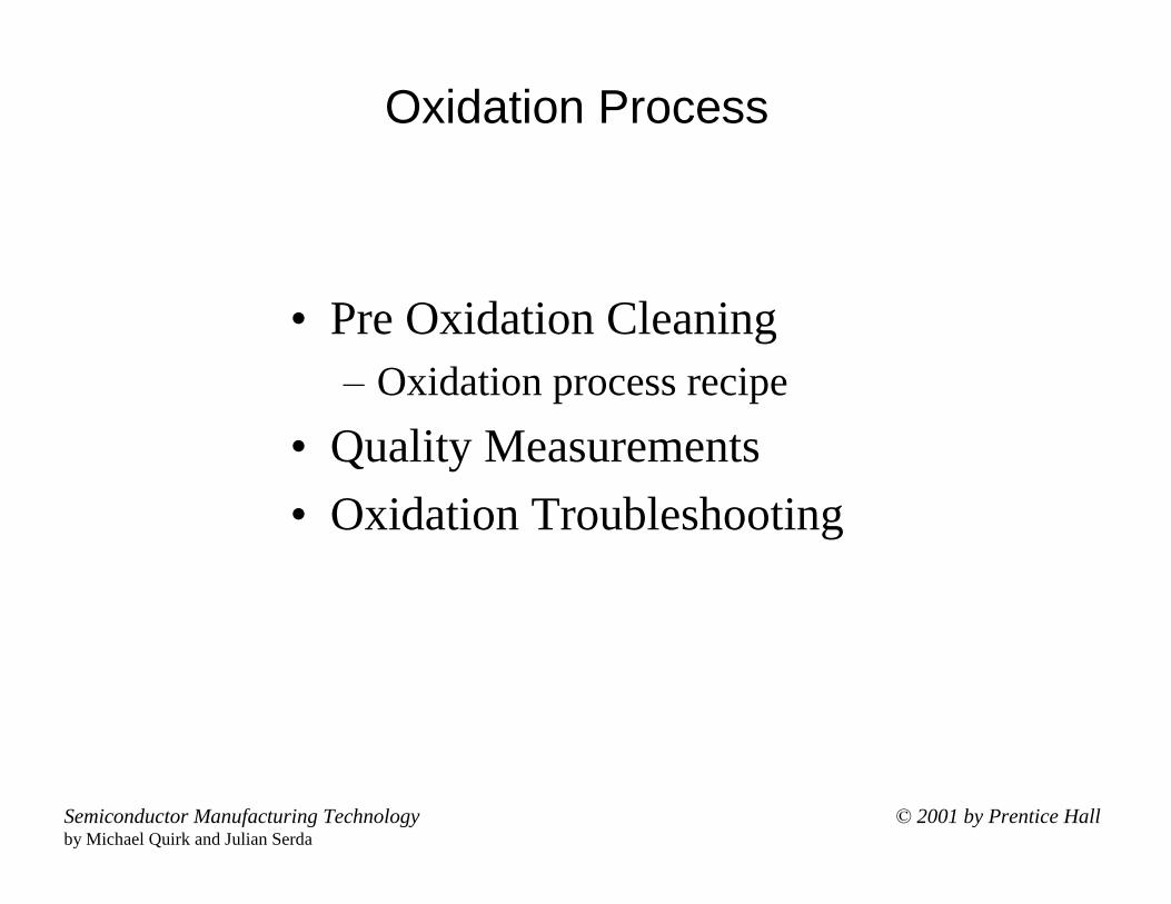
Oxidation Process
• Pre Oxidation Cleaning– Oxidation process recipe
• Quality Measurements• Oxidation Troubleshooting
© 2001 by Prentice HallSemiconductor Manufacturing Technologyby Michael Quirk and Julian Serda
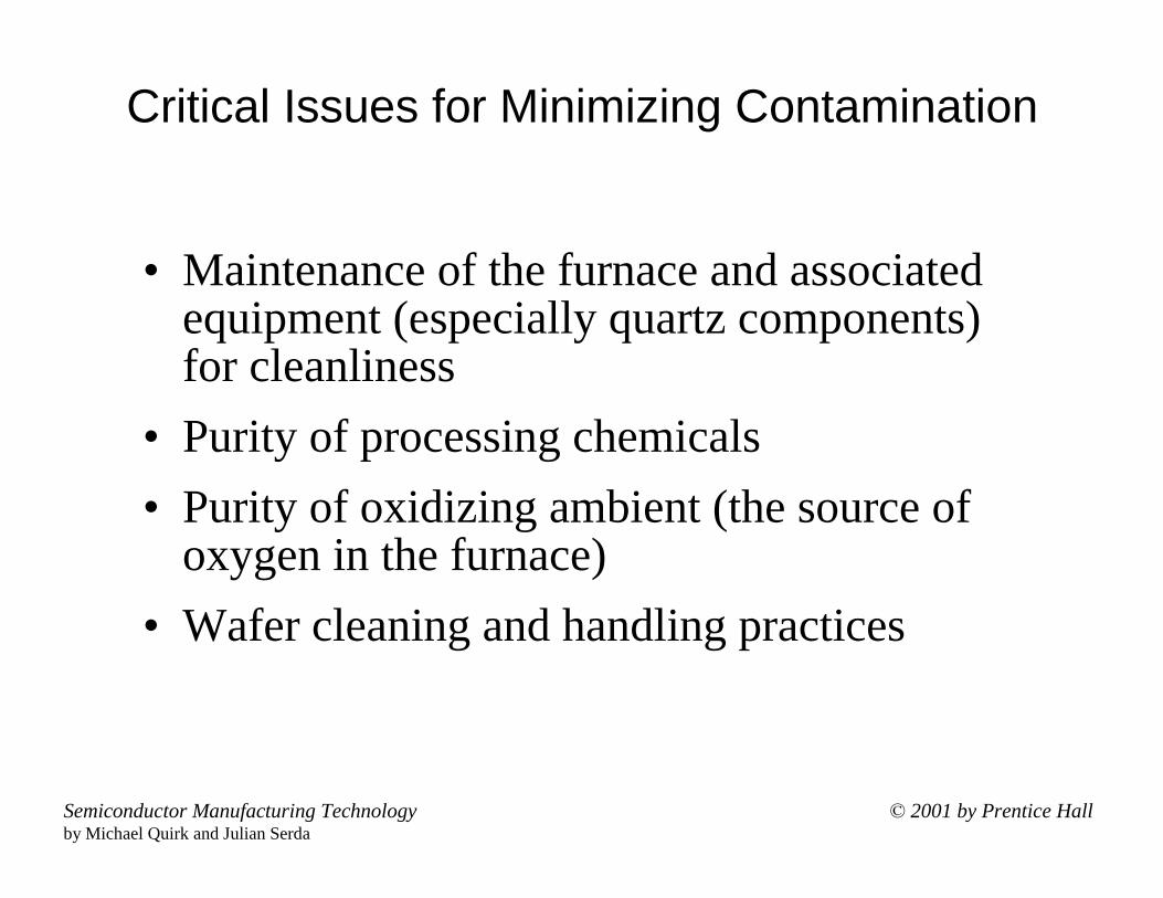
Critical Issues for Minimizing Contamination
• Maintenance of the furnace and associated equipment (especially quartz components) for cleanliness
• Purity of processing chemicals• Purity of oxidizing ambient (the source of
oxygen in the furnace)• Wafer cleaning and handling practices
© 2001 by Prentice HallSemiconductor Manufacturing Technologyby Michael Quirk and Julian Serda
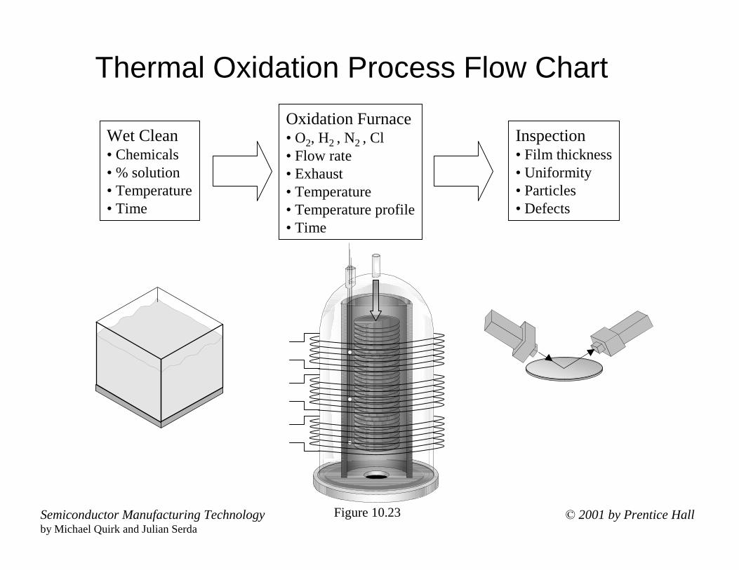
Thermal Oxidation Process Flow Chart
Wet Clean• Chemicals• % solution• Temperature• Time
Oxidation Furnace• O2, H2 , N2 , Cl• Flow rate• Exhaust• Temperature• Temperature profile• Time
Inspection• Film thickness• Uniformity• Particles• Defects
Figure 10.23
© 2001 by Prentice HallSemiconductor Manufacturing Technologyby Michael Quirk and Julian Serda
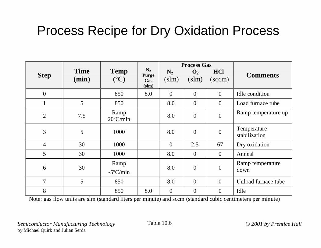
Process Recipe for Dry Oxidation Process
Step Time(min)
Temp(ºC)
N2PurgeGas(slm)
Process Gas N2 O2 HCl (slm) (slm) (sccm) Comments
0 850 8.0 0 0 0 Idle condition1 5 850 8.0 0 0 Load furnace tube
2 7.5 Ramp20ºC/min 8.0 0 0 Ramp temperature up
3 5 1000 8.0 0 0 Temperaturestabilization
4 30 1000 0 2.5 67 Dry oxidation5 30 1000 8.0 0 0 Anneal
6 30Ramp
-5ºC/min8.0 0 0
Ramp temperaturedown
7 5 850 8.0 0 0 Unload furnace tube8 850 8.0 0 0 0 Idle
Note: gas flow units are slm (standard liters per minute) and sccm (standard cubic centimeters per minute)
Table 10.6
© 2001 by Prentice HallSemiconductor Manufacturing Technologyby Michael Quirk and Julian Serda
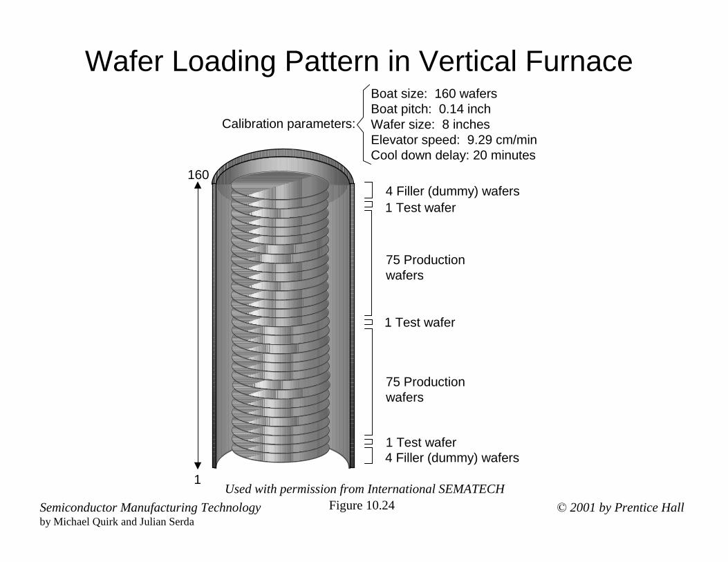
Wafer Loading Pattern in Vertical Furnace
160
1
4 Filler (dummy) wafers
4 Filler (dummy) wafers
1 Test wafer
1 Test wafer
1 Test wafer
75 Production wafers
75 Production wafers
Calibration parameters:
Boat size: 160 wafersBoat pitch: 0.14 inchWafer size: 8 inchesElevator speed: 9.29 cm/minCool down delay: 20 minutes
Figure 10.24Used with permission from International SEMATECH