
Roadmap Trends and Emerging Technologies -...
41
Roadmap Trends and Emerging Technologies Jim McElroy Bob Pfahl
Transcript of Roadmap Trends and Emerging Technologies -...
Roadmap Trends and
Emerging Technologies
Jim McElroy Bob Pfahl
1
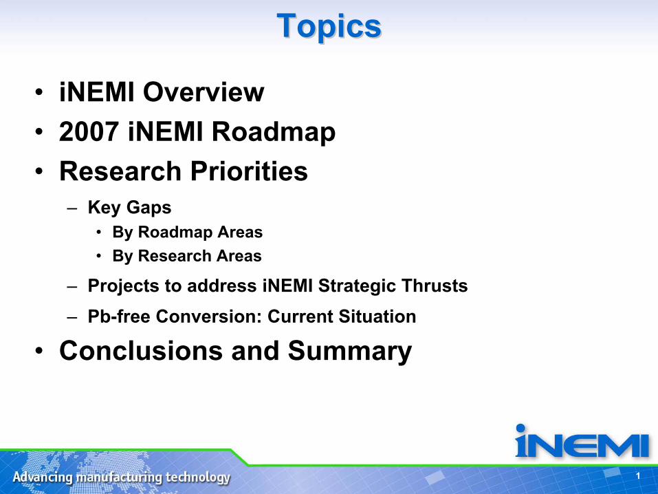
TopicsTopics
• iNEMI Overview• 2007 iNEMI Roadmap• Research Priorities
– Key Gaps• By Roadmap Areas• By Research Areas
– Projects to address iNEMI Strategic Thrusts– Pb-free Conversion: Current Situation
• Conclusions and Summary
2
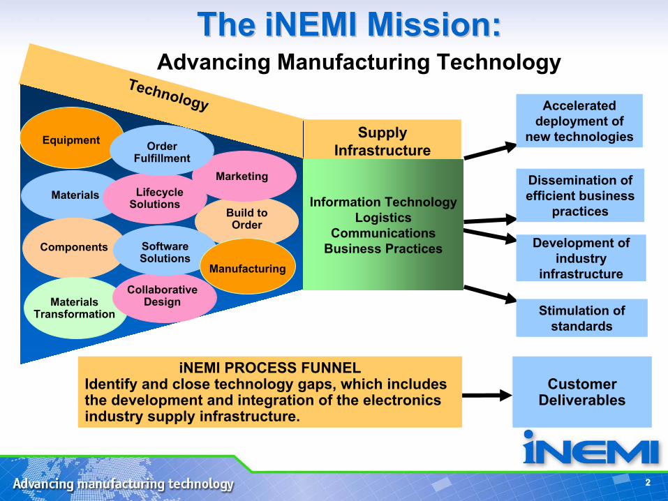
Technology
Supply Infrastructure
2
TheThe iNEMI Mission:iNEMI Mission:
Build toOrder
Materials
Components
Equipment
MaterialsTransformation
Collaborative Design
Lifecycle Solutions
Software Solutions
iNEMI PROCESS FUNNELIdentify and close technology gaps, which includes the development and integration of the electronics industry supply infrastructure.
Development of industry
infrastructure
Accelerated deployment of
new technologies
Dissemination of efficient business
practices
Stimulation of standards
Manufacturing
Marketing
Order Fulfillment
Customer Deliverables
Information TechnologyLogistics
CommunicationsBusiness Practices
Advancing Manufacturing Technology
2007 iNEMI Roadmap
4
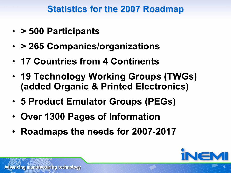
Statistics for the 2007 RoadmapStatistics for the 2007 Roadmap
• > 500 Participants• > 265 Companies/organizations• 17 Countries from 4 Continents• 19 Technology Working Groups (TWGs)
(added Organic & Printed Electronics)• 5 Product Emulator Groups (PEGs)• Over 1300 Pages of Information• Roadmaps the needs for 2007-2017
5
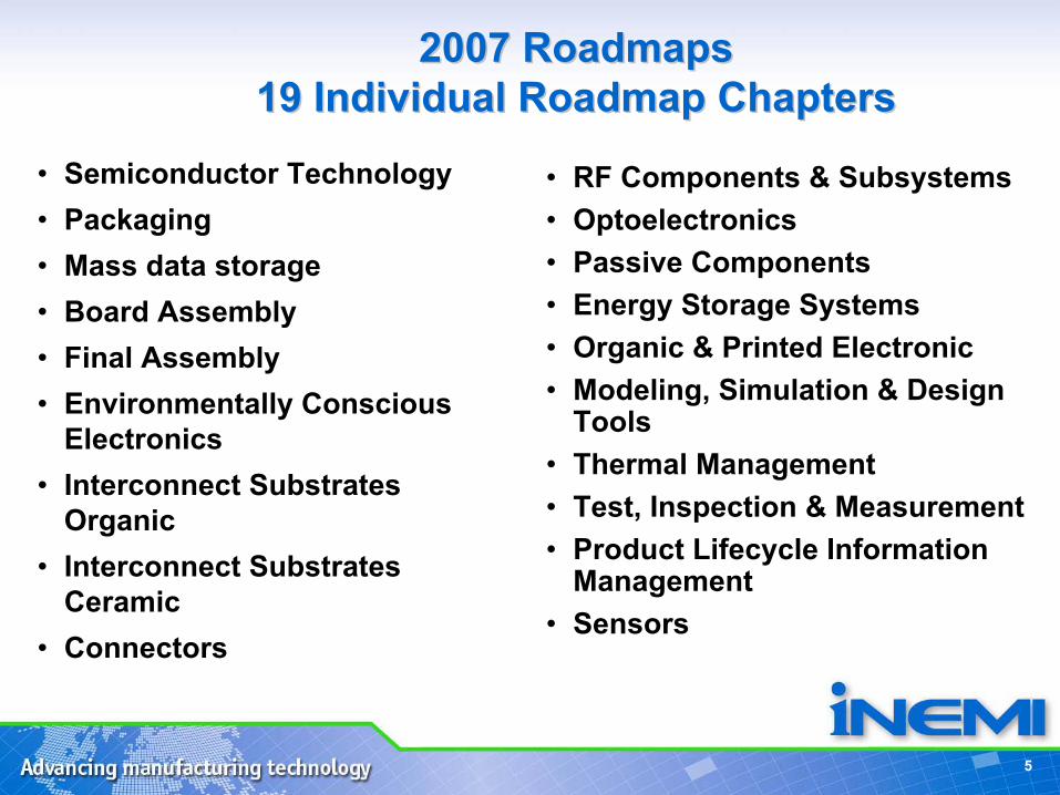
2007 Roadmaps 2007 Roadmaps 19 Individual Roadmap Chapters19 Individual Roadmap Chapters
• Semiconductor Technology• Packaging• Mass data storage• Board Assembly• Final Assembly• Environmentally Conscious
Electronics• Interconnect Substrates
Organic• Interconnect Substrates
Ceramic• Connectors
• RF Components & Subsystems• Optoelectronics• Passive Components• Energy Storage Systems• Organic & Printed Electronic• Modeling, Simulation & Design
Tools• Thermal Management• Test, Inspection & Measurement• Product Lifecycle Information
Management• Sensors
6
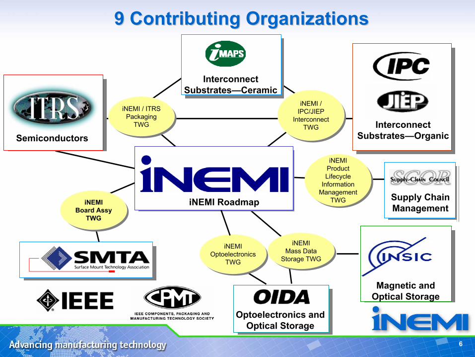
iNEMIOptoelectronics
TWG
iNEMIOptoelectronics
TWG
Optoelectronics and Optical Storage
Interconnect Substrates—Ceramic
InterconnectSubstrates—Organic
Magnetic and Optical Storage
Supply ChainManagement
Semiconductors
iNEMI Roadmap
iNEMIProduct Lifecycle
Information Management
TWG
iNEMIProduct Lifecycle
Information Management
TWG
iNEMIMass Data
Storage TWG
iNEMIMass Data
Storage TWG
iNEMI / IPC/JIEP
InterconnectTWG
iNEMI / IPC/JIEP
InterconnectTWG
iNEMI / ITRSPackaging
TWG
iNEMI / ITRSPackaging
TWG
iNEMIBoard Assy
TWG
iNEMIBoard Assy
TWG
9 Contributing Organizations9 Contributing Organizations
7
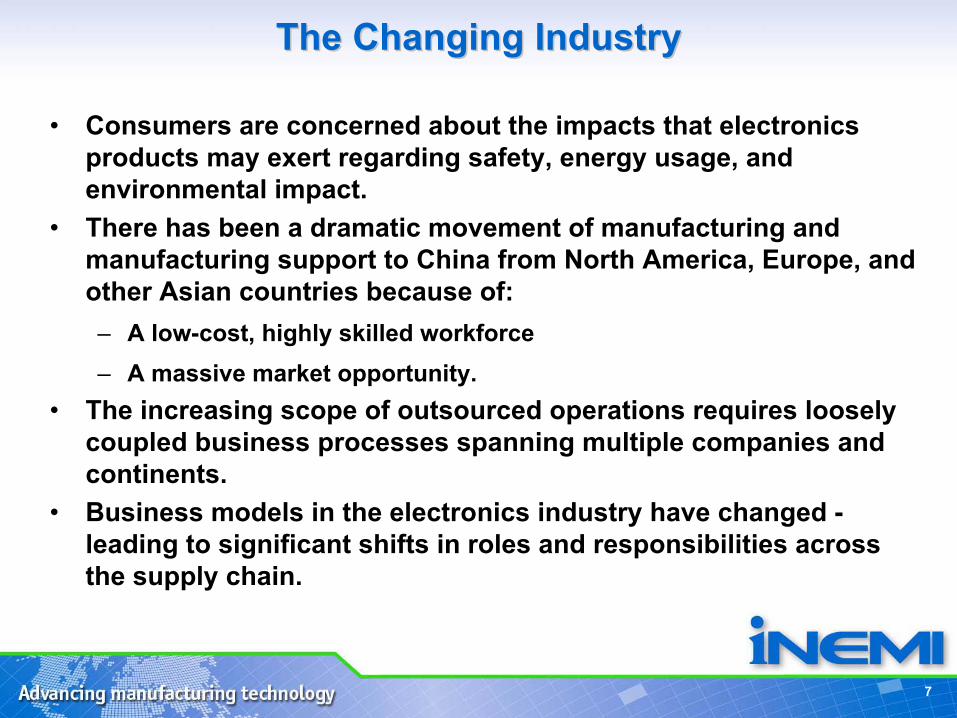
The Changing IndustryThe Changing Industry
• Consumers are concerned about the impacts that electronics products may exert regarding safety, energy usage, and environmental impact.
• There has been a dramatic movement of manufacturing and manufacturing support to China from North America, Europe, and other Asian countries because of: – A low-cost, highly skilled workforce– A massive market opportunity.
• The increasing scope of outsourced operations requires loosely coupled business processes spanning multiple companies and continents.
• Business models in the electronics industry have changed -leading to significant shifts in roles and responsibilities across the supply chain.
8
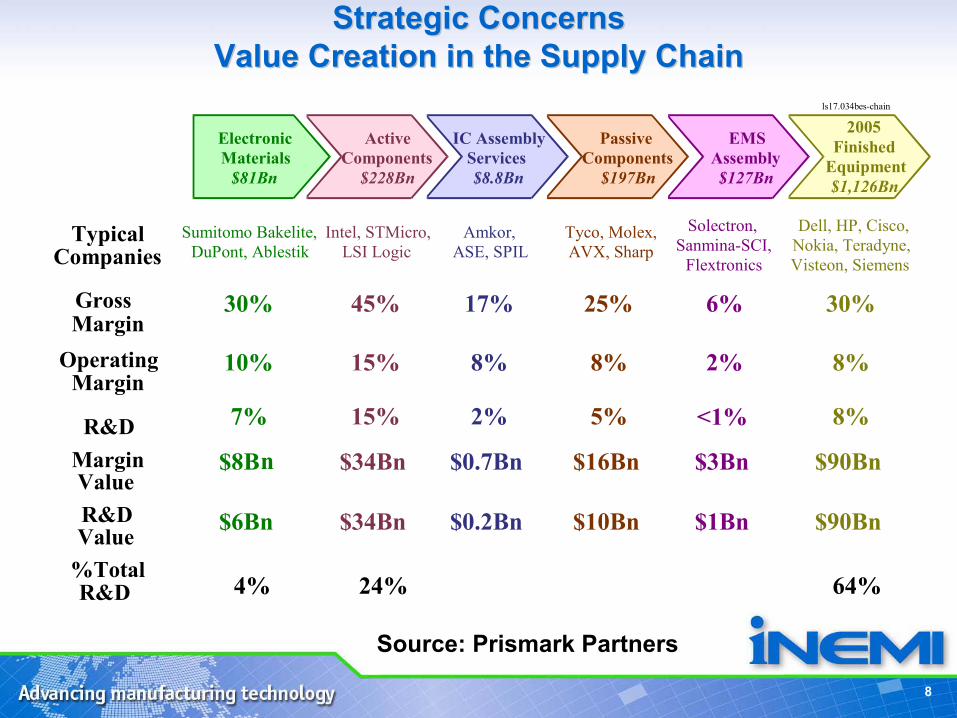
Electronic Materials$81Bn
ActiveComponents$228Bn
IC AssemblyServices$8.8Bn
PassiveComponents$197Bn
EMSAssembly$127Bn
2005Finished
Equipment$1,126Bn
Typical Companies
Sumitomo Bakelite,DuPont, Ablestik
Intel, STMicro,LSI Logic
Amkor, ASE, SPIL
Tyco, Molex,AVX, Sharp
Solectron, Sanmina-SCI,
Flextronics
Dell, HP, Cisco,Nokia, Teradyne,Visteon, Siemens
Gross Margin
30% 45% 17% 25% 6% 30%
Operating Margin
10% 15% 8% 8% 2% 8%
R&D 7% 15% 2% 5% <1% 8%
Margin Value
$8B n $34Bn $0.7Bn $16Bn $3Bn $90Bn
R&D Value $6Bn $34Bn $0.2Bn $10Bn $1Bn $90Bn
ls17.034bes-chain
%Total R&D 4% 24% 64%
Strategic ConcernsStrategic ConcernsValue Creation in the Supply ChainValue Creation in the Supply Chain
Source: Prismark Partners
9
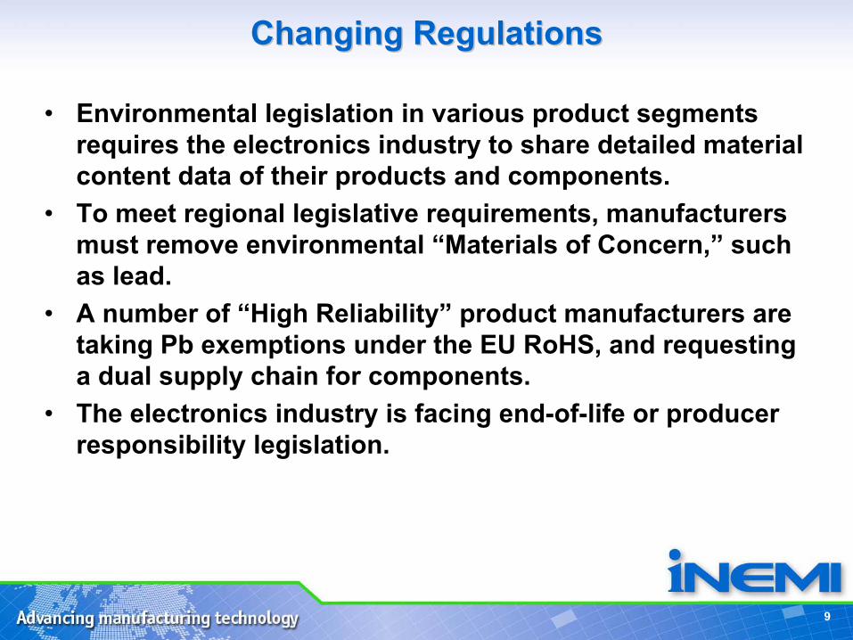
Changing RegulationsChanging Regulations
• Environmental legislation in various product segments requires the electronics industry to share detailed material content data of their products and components.
• To meet regional legislative requirements, manufacturers must remove environmental “Materials of Concern,” such as lead.
• A number of “High Reliability” product manufacturers are taking Pb exemptions under the EU RoHS, and requesting a dual supply chain for components.
• The electronics industry is facing end-of-life or producer responsibility legislation.
10
Market GrowthMarket Growth
• Worldwide production of computers and office equipment is expected to reach $431Bn in 2006, and grow at an average rate of5.4% per year to reach $532Bn in 2010.
• Global production of communications equipment is expected to reach $176Bn in 2006, representing about 15% of the electronics industry.
• Portable and consumer electronics production will reach $267Bn in 2006, following several years of exceptional growth.
• Medical electronics equipment production will be $53Bn in 2006, accounting for about 4% of the global electronics industry.
• In 2006, over 3Bn SiPs were assembled. By 2010, this number is expected to reach 6.65Bn, growing at an average rate of about 17% per year.
11
Converging MarketsConverging Markets
• Medical-Consumer
• Automotive-Entertainment
• Communication-Entertainment
• Computing-Entertainment
12
Emerging TechnologyEmerging Technology
• The end of traditional semiconductor scaling. • Reduction of emphasis on the microprocessor frequency
metric, and the corresponding increase in importance of the system’s throughput metric.
• Higher bandwidth to and from the microprocessor. • Increased need for improved cooling & reduced power.• Minaturization including 3D Packaging.• Disruptive technology offers opportunity for innovation. In
order to ensure success, the supply chain must be willing to invest with a long-term perspective in mind.
• The 2007 roadmap did not identify a major need for optical transmission within high performance printed wiring boards during the next decade.
• Growth in silicon device size is slowing.
Research Priorities
1414
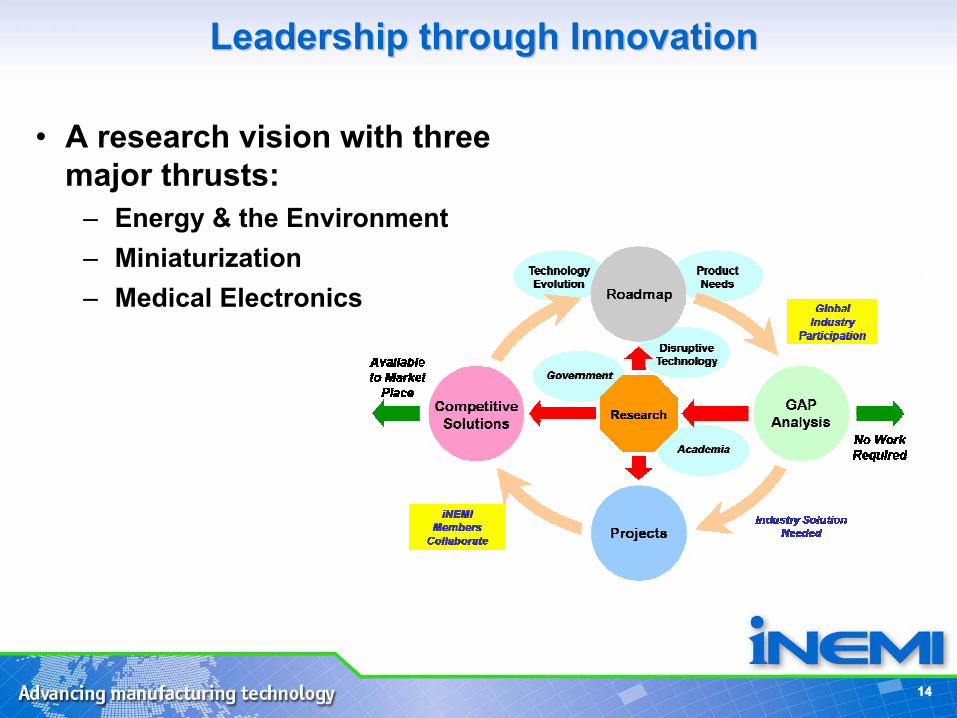
• A research vision with three major thrusts:
– Energy & the Environment– Miniaturization– Medical Electronics
Leadership through InnovationLeadership through Innovation
15
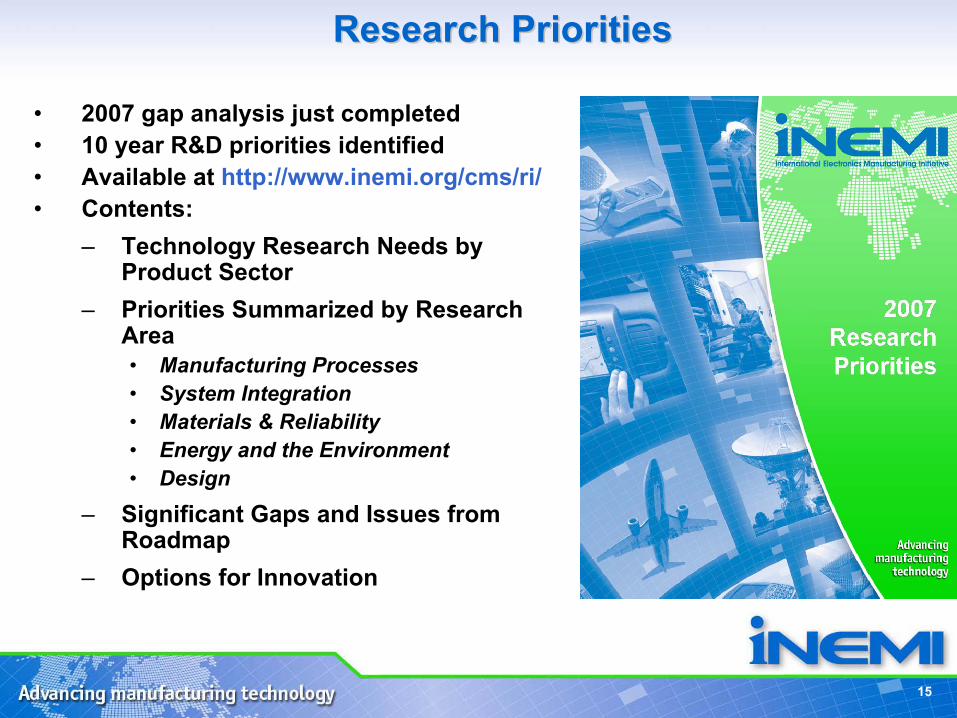
Research PrioritiesResearch Priorities
• 2007 gap analysis just completed• 10 year R&D priorities identified• Available at http://www.inemi.org/cms/ri/• Contents:
– Technology Research Needs by Product Sector
– Priorities Summarized by Research Area • Manufacturing Processes• System Integration• Materials & Reliability • Energy and the Environment• Design
– Significant Gaps and Issues from Roadmap
– Options for Innovation
16
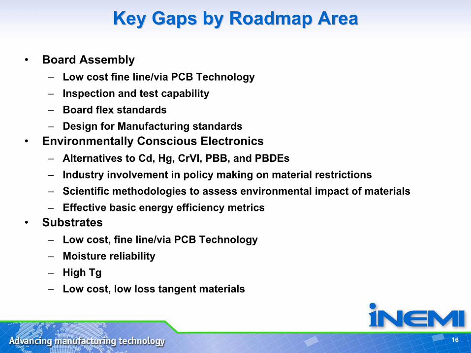
Key Gaps by Roadmap AreaKey Gaps by Roadmap Area
• Board Assembly– Low cost fine line/via PCB Technology– Inspection and test capability– Board flex standards– Design for Manufacturing standards
• Environmentally Conscious Electronics– Alternatives to Cd, Hg, CrVI, PBB, and PBDEs – Industry involvement in policy making on material restrictions – Scientific methodologies to assess environmental impact of materials – Effective basic energy efficiency metrics
• Substrates– Low cost, fine line/via PCB Technology– Moisture reliability– High Tg– Low cost, low loss tangent materials
17
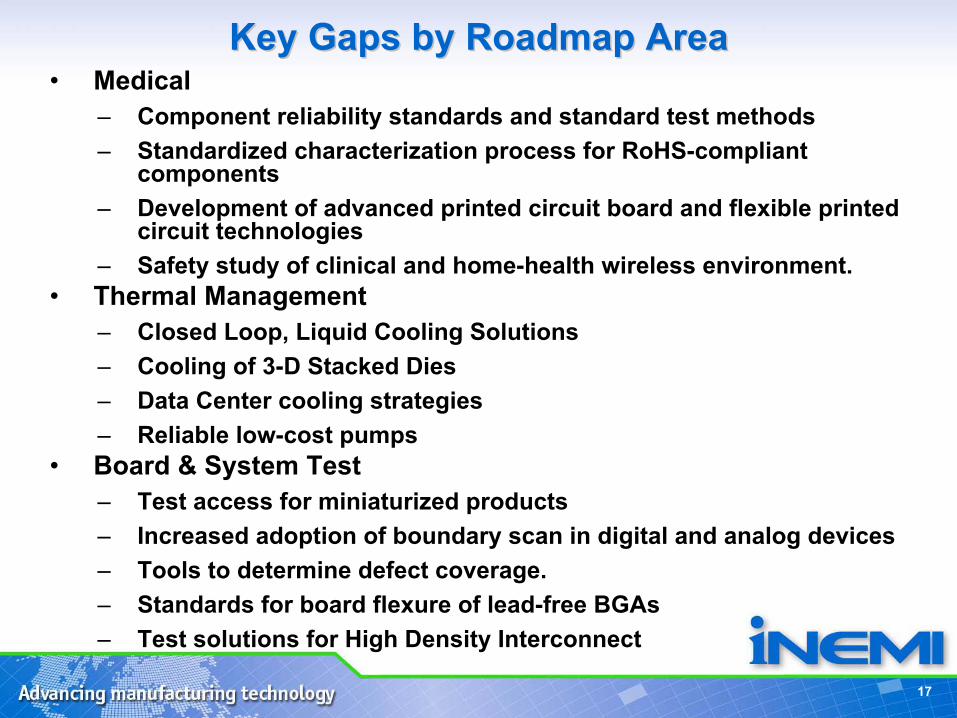
Key Gaps by Roadmap AreaKey Gaps by Roadmap Area• Medical
– Component reliability standards and standard test methods – Standardized characterization process for RoHS-compliant
components – Development of advanced printed circuit board and flexible printed
circuit technologies – Safety study of clinical and home-health wireless environment.
• Thermal Management – Closed Loop, Liquid Cooling Solutions– Cooling of 3-D Stacked Dies– Data Center cooling strategies– Reliable low-cost pumps
• Board & System Test– Test access for miniaturized products– Increased adoption of boundary scan in digital and analog devices – Tools to determine defect coverage. – Standards for board flexure of lead-free BGAs– Test solutions for High Density Interconnect
18
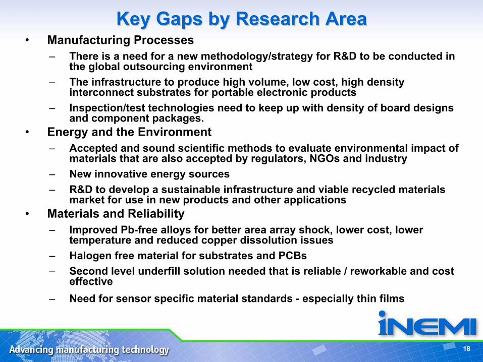
Key Gaps by Research AreaKey Gaps by Research Area• Manufacturing Processes
– There is a need for a new methodology/strategy for R&D to be conducted in the global outsourcing environment
– The infrastructure to produce high volume, low cost, high density interconnect substrates for portable electronic products
– Inspection/test technologies need to keep up with density of board designs and component packages.
• Energy and the Environment– Accepted and sound scientific methods to evaluate environmental impact of
materials that are also accepted by regulators, NGOs and industry – New innovative energy sources – R&D to develop a sustainable infrastructure and viable recycled materials
market for use in new products and other applications • Materials and Reliability
– Improved Pb-free alloys for better area array shock, lower cost, lower temperature and reduced copper dissolution issues
– Halogen free material for substrates and PCBs – Second level underfill solution needed that is reliable / reworkable and cost
effective– Need for sensor specific material standards - especially thin films
19
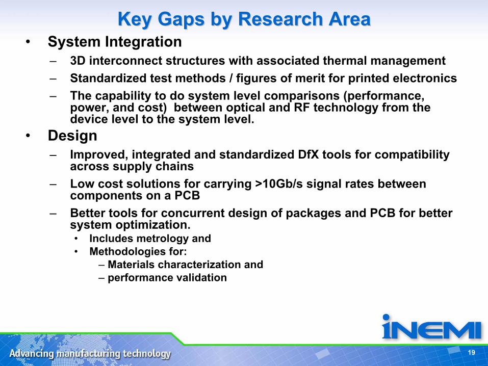
Key Gaps by Research AreaKey Gaps by Research Area• System Integration
– 3D interconnect structures with associated thermal management– Standardized test methods / figures of merit for printed electronics – The capability to do system level comparisons (performance,
power, and cost) between optical and RF technology from the device level to the system level.
• Design– Improved, integrated and standardized DfX tools for compatibility
across supply chains – Low cost solutions for carrying >10Gb/s signal rates between
components on a PCB – Better tools for concurrent design of packages and PCB for better
system optimization. • Includes metrology and • Methodologies for:
– Materials characterization and – performance validation
iNEMI Projects to
address Strategic
Thrusts
21
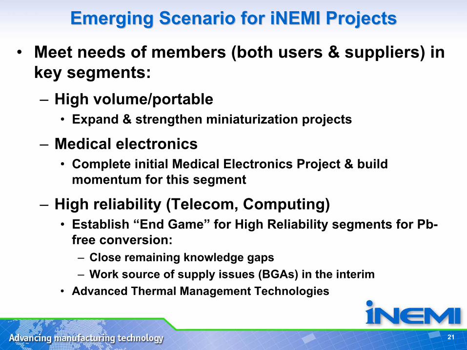
Emerging Scenario for iNEMI ProjectsEmerging Scenario for iNEMI Projects
• Meet needs of members (both users & suppliers) in key segments:– High volume/portable
• Expand & strengthen miniaturization projects
– Medical electronics• Complete initial Medical Electronics Project & build
momentum for this segment
– High reliability (Telecom, Computing)• Establish “End Game” for High Reliability segments for Pb-
free conversion:– Close remaining knowledge gaps– Work source of supply issues (BGAs) in the interim
• Advanced Thermal Management Technologies
22
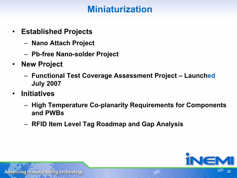
Miniaturization
• Established Projects– Nano Attach Project– Pb-free Nano-solder Project
• New Project– Functional Test Coverage Assessment Project – Launched
July 2007• Initiatives
– High Temperature Co-planarity Requirements for Components and PWBs
– RFID Item Level Tag Roadmap and Gap Analysis
23
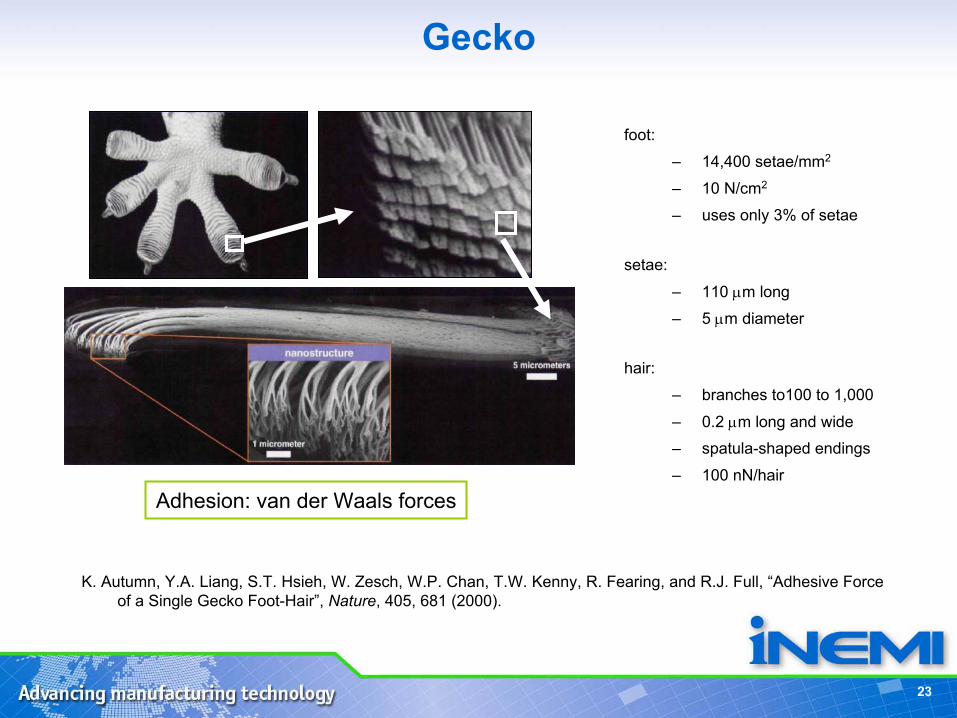
Gecko
K. Autumn, Y.A. Liang, S.T. Hsieh, W. Zesch, W.P. Chan, T.W. Kenny, R. Fearing, and R.J. Full, “Adhesive Force of a Single Gecko Foot-Hair”, Nature, 405, 681 (2000).
foot:
– 14,400 setae/mm2
– 10 N/cm2
– uses only 3% of setae
setae:
– 110 µm long
– 5 µm diameter
hair:
– branches to100 to 1,000
– 0.2 µm long and wide
– spatula-shaped endings
– 100 nN/hair
Adhesion: van der Waals forces
24
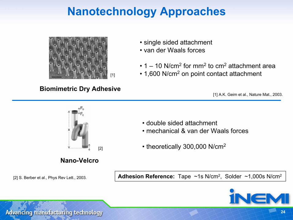
Nanotechnology Approaches
Nano-Velcro
[1] A.K. Geim et al., Nature Mat., 2003.Biomimetric Dry Adhesive
[1]
• single sided attachment• van der Waals forces
• 1 – 10 N/cm2 for mm2 to cm2 attachment area • 1,600 N/cm2 on point contact attachment
• double sided attachment• mechanical & van der Waals forces
• theoretically 300,000 N/cm2
Adhesion Reference: Tape ~1s N/cm2, Solder ~1,000s N/cm2
[2]
[2] S. Berber et al., Phys Rev Lett., 2003.
25
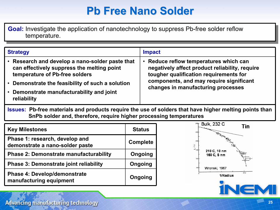
Strategy Impact• Research and develop a nano-solder paste that
can effectively suppress the melting point temperature of Pb-free solders
• Demonstrate the feasibility of such a solution• Demonstrate manufacturability and joint
reliability
• Reduce reflow temperatures which can negatively affect product reliability, require tougher qualification requirements for components, and may require significant changes in manufacturing processes
Issues: Pb-free materials and products require the use of solders that have higher melting points than SnPb solder and, therefore, require higher processing temperatures
Key Milestones StatusPhase 1: research, develop and demonstrate a nano-solder paste Complete
Phase 2: Demonstrate manufacturability Ongoing
Phase 3: Demonstrate joint reliability Ongoing
Phase 4: Develop/demonstrate manufacturing equipment Ongoing
Pb Free Nano Solder Pb Free Nano Solder Goal: Investigate the application of nanotechnology to suppress Pb-free solder reflow
temperature.Goal: Investigate the application of nanotechnology to suppress Pb-free solder reflow
temperature.
26
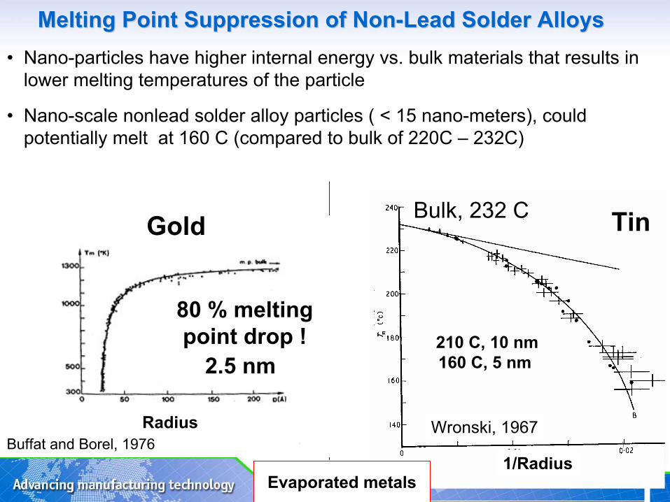
Gold
Radius
80 % melting point drop !
2.5 nm
Melting Point Suppression of NonMelting Point Suppression of Non--Lead Solder AlloysLead Solder Alloys• Nano-particles have higher internal energy vs. bulk materials that results in
lower melting temperatures of the particle
• Nano-scale nonlead solder alloy particles ( < 15 nano-meters), could potentially melt at 160 C (compared to bulk of 220C – 232C)
Evaporated metalsBuffat and Borel, 1976
TinBulk, 232 C
210 C, 10 nm160 C, 5 nm
Wronski, 1967
1/RadiusEvaporated metals
27
iNEMI RFID Item Level Tag Roadmap
ILT Roadmap – Why now?
– Major barriers exist at ILT RFID implementation
– To provide RFID stakeholders guidance for ILT infrastructure and supply chain development
– To drive ubiquitous deployment of RFID solutions
– The ILT roadmap effort is being driven by the RFID supply chain members
– This roadmap activity is open to all RFID stakeholders. Your participation is most welcome!
28
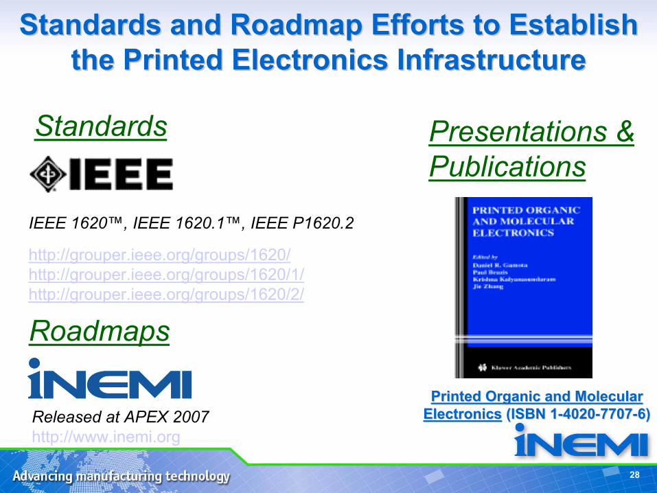
Standards and Roadmap Efforts to Establish Standards and Roadmap Efforts to Establish the Printed Electronics Infrastructurethe Printed Electronics Infrastructure
Standards
Roadmaps
Presentations & Publications
Printed Organic and Molecular Printed Organic and Molecular ElectronicsElectronics (ISBN 1(ISBN 1--40204020--77077707--6)6)
http://grouper.ieee.org/groups/1620/http://grouper.ieee.org/groups/1620/1/http://grouper.ieee.org/groups/1620/2/
Released at APEX 2007http://www.inemi.org
IEEE 1620™, IEEE 1620.1™, IEEE P1620.2
29
Medical Electronics
• Established Project– Medical Grade Component Reliability Specifications
• Initiative– iNEMI Substrates for Medical Devices
30
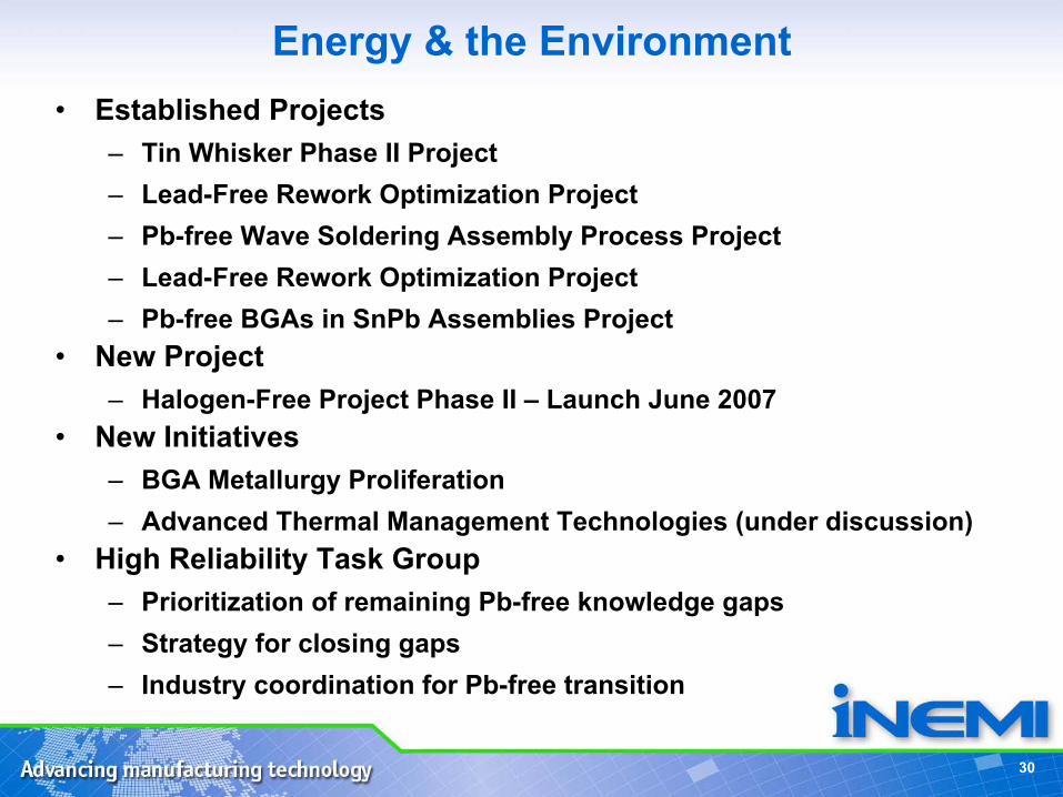
Energy & the Environment• Established Projects
– Tin Whisker Phase II Project – Lead-Free Rework Optimization Project– Pb-free Wave Soldering Assembly Process Project – Lead-Free Rework Optimization Project– Pb-free BGAs in SnPb Assemblies Project
• New Project– Halogen-Free Project Phase II – Launch June 2007
• New Initiatives– BGA Metallurgy Proliferation– Advanced Thermal Management Technologies (under discussion)
• High Reliability Task Group– Prioritization of remaining Pb-free knowledge gaps– Strategy for closing gaps– Industry coordination for Pb-free transition
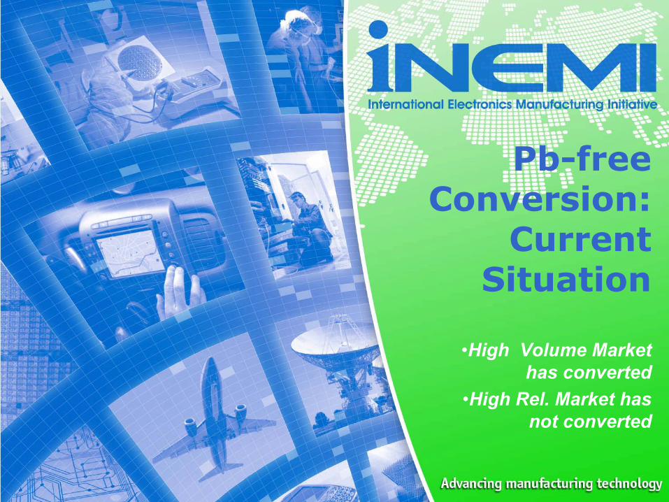
Pb-free Conversion:
Current Situation
•High Volume Market has converted
•High Rel. Market has not converted
32
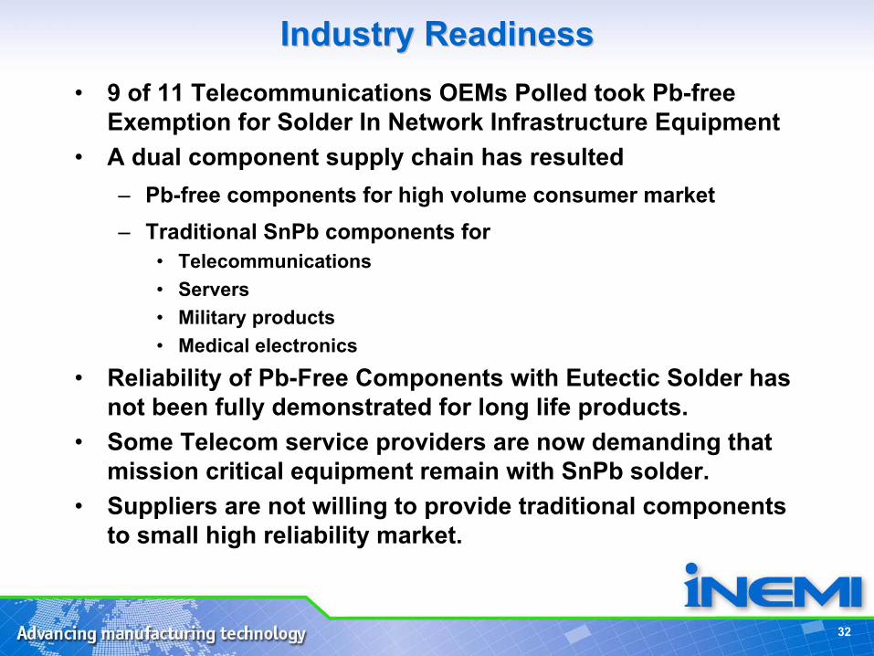
Industry ReadinessIndustry Readiness• 9 of 11 Telecommunications OEMs Polled took Pb-free
Exemption for Solder In Network Infrastructure Equipment• A dual component supply chain has resulted
– Pb-free components for high volume consumer market– Traditional SnPb components for
• Telecommunications• Servers• Military products• Medical electronics
• Reliability of Pb-Free Components with Eutectic Solder has not been fully demonstrated for long life products.
• Some Telecom service providers are now demanding that mission critical equipment remain with SnPb solder.
• Suppliers are not willing to provide traditional components to small high reliability market.
33
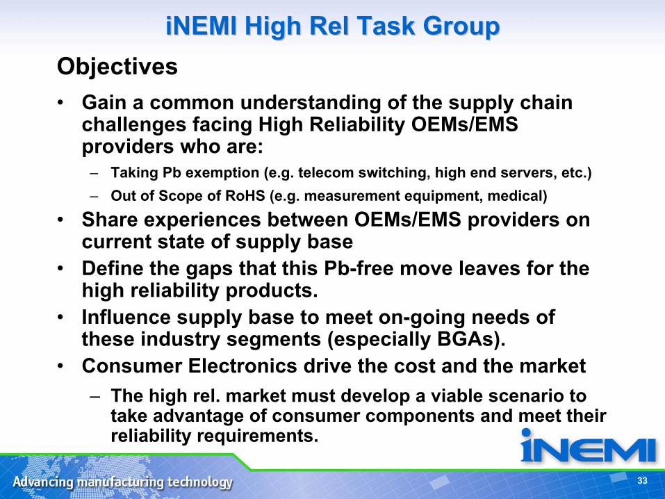
iNEMI High Rel Task GroupiNEMI High Rel Task GroupObjectives• Gain a common understanding of the supply chain
challenges facing High Reliability OEMs/EMS providers who are:
– Taking Pb exemption (e.g. telecom switching, high end servers, etc.)– Out of Scope of RoHS (e.g. measurement equipment, medical)
• Share experiences between OEMs/EMS providers on current state of supply base
• Define the gaps that this Pb-free move leaves for the high reliability products.
• Influence supply base to meet on-going needs of these industry segments (especially BGAs).
• Consumer Electronics drive the cost and the market– The high rel. market must develop a viable scenario to
take advantage of consumer components and meet their reliability requirements.
34
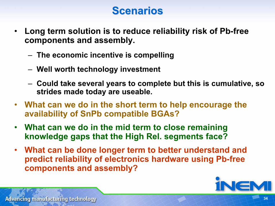
ScenariosScenarios
• Long term solution is to reduce reliability risk of Pb-free components and assembly.
– The economic incentive is compelling
– Well worth technology investment
– Could take several years to complete but this is cumulative, so strides made today are useable.
• What can we do in the short term to help encourage the availability of SnPb compatible BGAs?
• What can we do in the mid term to close remaining knowledge gaps that the High Rel. segments face?
• What can be done longer term to better understand and predict reliability of electronics hardware using Pb-free components and assembly?
35
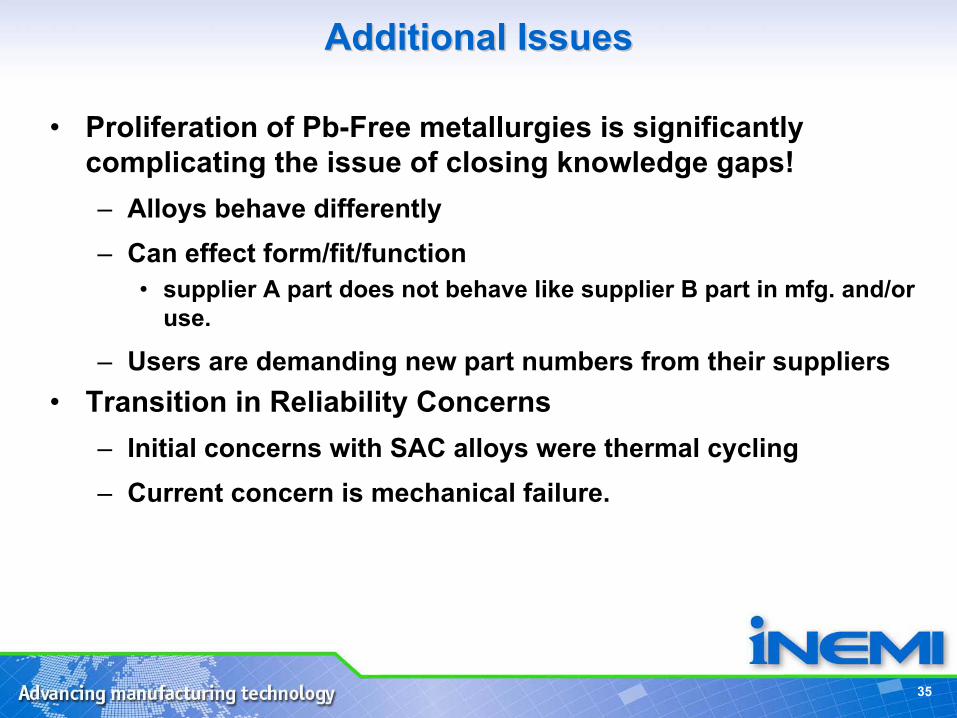
Additional IssuesAdditional Issues
• Proliferation of Pb-Free metallurgies is significantly complicating the issue of closing knowledge gaps!– Alloys behave differently– Can effect form/fit/function
• supplier A part does not behave like supplier B part in mfg. and/or use.
– Users are demanding new part numbers from their suppliers• Transition in Reliability Concerns
– Initial concerns with SAC alloys were thermal cycling– Current concern is mechanical failure.
36
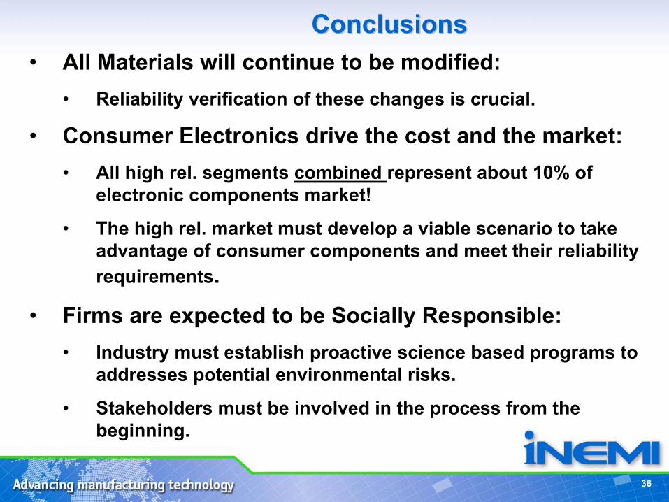
ConclusionsConclusions• All Materials will continue to be modified:
• Reliability verification of these changes is crucial.
• Consumer Electronics drive the cost and the market:• All high rel. segments combined represent about 10% of
electronic components market!
• The high rel. market must develop a viable scenario to take advantage of consumer components and meet their reliability requirements.
• Firms are expected to be Socially Responsible:• Industry must establish proactive science based programs to
addresses potential environmental risks.
• Stakeholders must be involved in the process from the beginning.
Conclusions & Summary
38
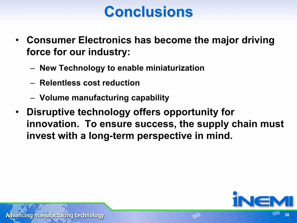
ConclusionsConclusions
• Consumer Electronics has become the major driving force for our industry:– New Technology to enable miniaturization
– Relentless cost reduction
– Volume manufacturing capability
• Disruptive technology offers opportunity for innovation. To ensure success, the supply chain must invest with a long-term perspective in mind.
39
SummarySummary
• The 2007 iNEMI Research Priorities identifies R&D needs that must be met.
• Given the limited resources that industry, academia, and governments can apply, it is crucial that we focus our R&D efforts on these high priority knowledge gaps.