PWBroadmap for Smartphone -...
17
Ibiden Confidential Page 1 PWB roadmap for Smartphone IBIDEN CO., LTD. Hirotaka Taniguchi IBIDEN CONFIDENTIAL
Transcript of PWBroadmap for Smartphone -...

Ibiden Confidential Page 1
PWBroadmap for Smartphone
IBIDENCO.,LTD.Hirotaka Taniguchi
IBIDEN CONFIDENTIAL
Ibiden Confidential Page 2
【Agenda】
1.Ibiden Introduction
2.Phone & PWB Trend
3.PWB Technology & Roadmap for Smartphone
4.Summary
IBIDEN CONFIDENTIAL

Ibiden Confidential Page 3
IBIDEN products overview
PWB
for Mobile
PKG
for PC/Server
CSP
(Chip Scale Package)
for Mobile
DPF
Housing material
Construction
Smartphone & Tablet;> 90%
IBIDEN CONFIDENTIAL

Ibiden Confidential Page 4
IBIDEN USA Corp.
Finnish BranchIBIDEN Europe B.V.
IBIDEN Electronics (Shanghai) Co.,Ltd.
IBIDEN Philippines,Inc.IBIDEN (Malaysia) SDN. BHD
IBIDEN SingaporePTE. LTD
IBIDEN Taiwan Co.Ltd.
IBIDEN Electronics (Beijing) Co., Ltd.
Dallas
Phoenix
Sunnyvale IBIDEN DPF France S. A. S
IBIDEN UK Ltd.
IBIDEN Deutschland GmbH
IBIDEN France S. A. S. IBIDEN Korea Co., Ltd.
IBIDEN Co. ,Ltd.
IBIDEN CANADAIBIDEN InternationalCo.,Ltd.
Detroit
IBIDEN Hungary Kft.
IBIDEN IndiaBangalore
IBIDEN VietnamHo Chi Minh
Electronic
Customer support officeCeramic
Micro-Mech, Inc.
IBIDEN Electronics Technology(Shanghai) Co.,Ltd.
Global Networkfor PWBIBIDEN Beijing IBIDEN Aoyanagi
IBIDEN Malaysia
IBIDEN CONFIDENTIAL

Ibiden Confidential Page 5
【Agenda】
1.Ibiden Introduction
2.Phone & PWB Trend
3.PWB Technology & Roadmap for Smartphone
4.Summary
IBIDEN CONFIDENTIAL
Ibiden Confidential Page 6
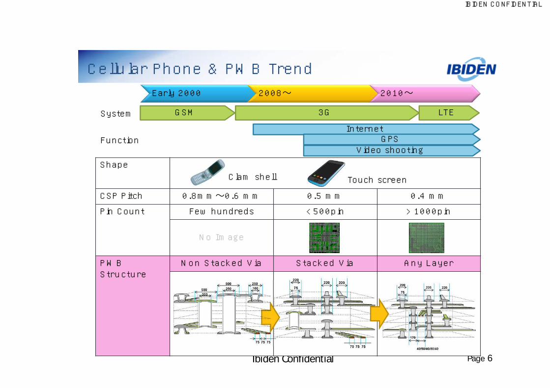
Shape
CSP Pitch 0.8mm〜0.6 mm 0.5 mm 0.4 mmPin Count Few hundreds <500pin >1000pin
No Image
PWBStructure
Non Stacked Via Stacked Via Any Layer
Early 2000 2008〜 2010〜
GSM 3G LTEInternet
GPSVideo shooting
Clam shell Touch screen
System
Function
Cellular Phone & PWB Trend
IBIDEN CONFIDENTIAL

Ibiden Confidential Page 7
IBIDEN will provide PWB solution for future smartphone.
Impedance control
Thinner PWB
Smaller board to keep battery area
Increase number of componentsFine pitch component
Thinner / Lighter
More Function
LongerBatteryHigher Speed
AnyLayerFineLine/SpaceLow Dk Material
Low Dk Material
Smartphone & PWB Trend
AnylayerFine Line/Space
AnylayerFine Line/Space
Any Layer + Fine L/S
IBIDEN CONFIDENTIAL

Ibiden Confidential Page 8
【Agenda】
1.Ibiden Introduction
2.Phone & PWB Trend
3.Ibiden PWB Technology & Roadmap for Smartphone
4.Summary
IBIDEN CONFIDENTIAL

Ibiden Confidential Page 9
Laser drilling
Filled via plating
Pattern Formation
Lamination Press
Laser drilling
Filled via plating
Repeating process
Copper Clad laminate
Ibiden Any Layer (FVSS3) Process Flow
Pattern Formation
IBIDEN CONFIDENTIAL

Ibiden Confidential Page 10
0.4mmP design optionCSP pitch 0.4 mmPatterning Subtractive ←
Main routing
Top view
L/S 60/60 um ←Via/pad 75/220 um ←Alignment +/-72.5 um ←
Partly routing
Top view
L/S 40/40 um 40/50 umVia/pad 75/200 um 75/170 umAlignment +/-62.5 um +/-47.5 um
Cu thickness is assumed to be 20um
Two lines between pads with 0.4 mmP are available.
IBIDEN CONFIDENTIAL

Ibiden Confidential Page 11
Technology
FVSS1(stacked via)
FVSS3(Any Layer) e-Flex Cavity
NoPhoto NoPhoto
Feature High densityHigh densityMiniaturizationThinner profile
High densityMiniaturizationThinner profile
High densityThinner profile
Surface Finish
ENIGSelective NiAuOSP
ENIGSelective NiAuOSP
ENIGSelective NiAuOSP
ENIGSelective NiAuOSP
Technology Line Up
We can support all technology to achieve smartphone requirement.
IBIDEN CONFIDENTIAL

Ibiden Confidential Page 12
2011 2012 2013 2014 2015
CSP Pitch 0.4 mmP 0.4 mmP 0.4 mmP 0.4 mmP 0.3 mmP
Line/Space 50/50 um 50/50 um 40/50 um 40/50 um 30/30 um
Via/Land 75/220 um 75/200 um 75/170 um 75/170 um 75/150 um
# of Line (s)btwn pads 1 1 2 2 2
Layer Count ~ 10layer ~ 12layer ~ 12layer ~ 12layer ~ 14layer
Patterning Subtractive Subtractive Subtractive Subtractive M-SAP
Dielectricmaterial
Conventional Conventional Conventional ConventionalLow Dk
ConventionalLow Dk
PWB Roadmap
At 0.3 mmP, M-SAP will be implemented.M-SAP: Modified Semi Additive Process
IBIDEN CONFIDENTIAL

Ibiden Confidential Page 13
Fine patterning tech. segmentation
M-SAP is next generation patterning process for PWBto achieve finer L/S.
60/60 50/50 40/50 30/30 25/25
5
10
15
20
25
SubtractiveM-SAP
SAP
40/40 35/35 20/20 10/10 5/5
L/S(um)
Cu th
ickn
ess (
um)
IBIDEN CONFIDENTIAL

Ibiden Confidential Page 14
0.4 mmP & 0.3 mmP design optionCSP pitch 0.4 mm 0.3 mm
Main routing
Top view
L/S 60/60 um ← ←Via/pad 75/220 um ← ←Alignment +/-72.5 um ← ←
Partly routing
Top view
L/S 40/40 um 40/50 um 30/30 umVia/pad 75/200 um 75/170 um 75/150 umAlignment +/-62.5 um +/-47.5 um +/-37.5 um
Cu thickness is assumed to be 20um
Two lines between pads with 0.3 mmP are available.
IBIDEN CONFIDENTIAL

Ibiden Confidential Page 15
【Agenda】
1.Ibiden Introduction
2.Phone & PWB Trend
3.PWB Technology & Roadmap for Smartphone
4.Summary
IBIDEN CONFIDENTIAL

Ibiden Confidential Page 16
Summary
CSP Pitch is key parameter for future smartphone PWB requirement.
Current: Two lines between pads with 0.4 mmP are available by subtractive.
Future: Two lines between pads with 0.3 mmP will be available by M-SAP.
IBIDEN CONFIDENTIAL

Ibiden Confidential Page 17
Thank you!
IBIDEN CONFIDENTIAL