MESSAGE FROM CHAIRMAN & CEO -...
22
Transcript of MESSAGE FROM CHAIRMAN & CEO -...


Advancing manufacturing technology 1
MESSAGE FROM CHAIRMAN & CEO2012 was our third successive year of strong membership growth and of broadening our collaborative project portfolio. This was accomplished in a year where the industry was challenged with major market changes and uncertain levels of economic growth. The continuing economic struggles in Europe, growth rate reductions in China and India, and sluggish economies in America and Japan left many industry executives in a conservative investment frame of mind. Despite this backdrop, iNEMI welcomed 14 new members in 2012, and we are proud to say that our international strength continues to grow with six of these new members headquartered in Asia and two in Europe. With a total membership of 107, we are now well positioned to have critical mass participation from up and down the industry supply chain plus from research groups on virtually all of our new collaborative R&D projects.
We ended the year having completed ten projects. All had end-of-project webinars or, in the case of white papers, widespread media publication. We also started 11 new projects in 2011, and eight of those were in areas that were new for iNEMI.
These new projects are addressing such issues as packaging equipment standardization, UL PCB and laminate certification, PCBA reliability qualification, warpage characteristics of organic packages, and MEMS sensors. In fact, we ended the year with two new MEMS projects approved and open for sign-up that are scheduled to launch in Q1 2013. The MEMS sensor market has truly exploded in the past 12 months and will continue to grow rapidly in the future. Thus, the timing is excellent for our collaborative efforts to improve the efficiency of reliability testing and of production testing key to these new sensor technologies.
In Q4 we completed a member survey regarding interest levels for new initiatives and subsequent projects in 2013. New projects were identified by year-end, and we will form new teams in the first half of 2013 to address key industry gaps.
We held excellent workshops on MEMS in Pittsburgh and on environmental opportunities at Electronics Goes Green in Berlin; and we hosted workshops for the 2013 Roadmap in the United States, Germany and Hong Kong. In fact, as 2012 came to an end, we were wrapping up another successful roadmap cycle. We had greater participation than ever before, with significant growth in the contributions coming from Europe and Asia, assuring a well-rounded, global perspective.
In summary, 2012 was another year of progress for iNEMI. We want to thank our entire membership for their support, and we are looking forward to additional momentum and growth of value for our members in 2013.
Nas
ser
Gra
yeli
Bill
Bad
er
Bill Bader
Executive Director & CEO iNEMI
Nasser Grayeli
Chairman, iNEMI Board of Directors Vice President Technology and Manufacturing Director of Corporate Quality Network Intel Corporation

2 iNEMI Progress 2012
INCREASING OuR NuMBERS GlOBAlly iNEMI saw another year of strong membership growth during 2012. Despite continued economic challenges around the world, we were able to add 14 new members to our roster, bringing our total membership to 107 by the end of the year (see Table 1). New projects in medical electronics attracted several new members, while reliability studies were also a big draw.
Table 1. 2012 New Members
Organization location Business Type iNEMI Interests
Assembléon Netherlands NetherlandsEquipment supplier
Packaging standardization
CALCE (Center for Advanced Life Cycle Engineering)/University of Maryland
USAUniversity research
Medical & reliability studies
Cochlear Limited Australia OEM Medical projects
Exponent, Inc. USA Consultant Medical projects
Griffith University AustraliaUniversity research
Miniaturization
Hitachi Chemical Co., Ltd. JapanMaterials supplier
Various packaging projects
IEC Electronics USA EMS High reliability
KXI (Shenzhen Kunqi Xinhua Technology Co., Ltd.)
ChinaMaterials supplier
Networking contacts
Lotes Co., Ltd. TaiwanMaterials supplier
Networking contacts, projects to be determined
NAMICS Corporation JapanMaterials supplier
Advanced underfill
Nordson Advanced Technology Systems Business Group
USAEquipment supplier
Packaging projects, networking contacts
OIDA (Optoelectronics Industry Development Association)
USA AssociationOptoelectronics roadmap
Valtronic Technologies Switzerland EMS Medical projects
Wistron Corporation Taiwan ODM Various projects
More than half of the organizations that joined iNEMI in 2012 are headquartered in Asia and Europe, thus continuing the expansion of our international presence. As a reflection of the ever-increasing importance of these regions, the iNEMI staff coordinators there have become managing directors. Haley Fu is now Managing Director of Asia Pacific, and Grace O’Malley is Managing Director of EMEA.
Table of ContentsMESSAGE FROM CHAIRMAN & CEO 1
INCREASING OuR NuMBERS GlOBAlly 2
ExpANdING OuR RESEARCH pROGRAM 3
FOCuSING ON THE FuTuRE: THE 2013 ROAdMAp 4
SETTING THE 2013 COllABORATION AGENdA 5
BROAdENING OuR pROjECT pORTFOlIO 6
dElIvERING RESulTS 10
2012 INEMI MEMBERS 20
CONTACT uS 20
Gra
ce O
’Mal
ley
Hal
ey F
u

Advancing manufacturing technology 3
iNEMI is partnering with member Purdue University, along with Tuskegee University, on an international effort to replace conventional electronics with more sustainable technologies and train a workforce of specialists to make the transition possible. The university-based Global Traineeship in Sustainable Electronics is funded with a five-year, $3.2 million grant from the National Science Foundation’s Integrative Graduate Education and Research Traineeship (IGERT) program.
The Sustainable Electronics program combines education and training of future engineers with research to develop new, more environmentally friendly and sustainable materials. Carol Handwerker, Purdue’s Reinhardt Schuhmann Jr. Professor of Materials Engineering and co-chair of the iNEMI Research Committee, is principal investigator for the project.
“We want to create materials that will allow computer components to be disassembled, recycled and reused,” said Handwerker. “The traditional, linear model of consumption — ‘design it, build it, use it, throw it away’ — has long ceased being viable for electronics. That is why we proposed this innovative,
integrative global education and research program to educate and train a Ph.D. workforce with an unprecedented capacity for analyzing complex dynamic systems.”
The Sustainable Electronics program will focus on three areas of research: (1) creation of polymers from nature for construction and disassembly, (2) development of methods and metrics to support sustainable product design and manufacture and (3) system and supply chain issues.
iNEMI and six committed industry partners – iNEMI members Alcatel-Lucent, Celestica, Cisco, Dell and Intel, plus Heritage Environmental Services – will participate throughout the education, research, and training program, providing, for example, sponsorship of cross-disciplinary project topics for IGERT student teams and industrial internship experiences to put the program’s curriculum into practice.
Robert Pfahl, iNEMI’s Vice President of Global Operations, will serve on the External Advisory Board for the Sustainable Electronics program, along with other industry representatives. He will also assist with international coordination of the program.
ExpANdING OuR RESEARCH pROGRAMIn 2012 iNEMI expanded our involvement and integration with the research community, seeking collaboration opportunities for iNEMI as well as for individual member companies. We arranged four webinars in which research institutes or universities presented information about key research programs to interested iNEMI member companies. These webinars gave the research groups visibility in front of our industrial members while, at the same time, making our industrial members aware of research relevant to their respective areas of business. The University of California at Davis, Rochester Institute of Technology (RIT), Massachusetts Institute of Technology (MIT) and City University of Dublin all made presentations to select members.
iNEMI currently has a collaborative research effort under way with Purdue University. This effort, funded by the National Science Foundation, requires industrial partners for success; and iNEMI, along with five of our industry members, are involved with this multi-year program (see below for details).
Car
ol H
and
we
rke
r
iNEMI pARTNERS wITH puRduE
ON SuSTAINABlE ElECTRONICS
4 iNEMI Progress 2012
FOCuSING ON THE FuTuRE: THE 2013 ROAdMApThe 2013 Roadmap was a major focus of activity throughout 2012. Public meetings, such as the Technology Working Group (TWG) kick-off at APEX, the Product Emulator Group (PEG) webinars, and regional workshops held in North America (San Diego), Asia (Hong Kong) and Europe (Berlin), were coupled with regular meetings of the various working groups and face-to-face meetings with the iNEMI Technical Committee. More than 650 participants — the largest number ever — from 350 organizations in 18 countries invested more than seven man-years to develop this latest roadmap.
paradigm Shifts IdentifiedThe 2013 Roadmap looks at six product sectors and 20 technology and business process areas. Among other things, it identifies significant paradigm shifts in the various technology areas. The most important shift identified in the 2013 Roadmap is the impact of cloud-connected digital devices. The movement to the cloud, coupled with the uncertainty regarding what type of “terminal” devices the market will favor (PC, tablet, smart phone, TV), has the potential to cause major disruptions across the industry. In the next four to five years, the industry is likely to see major transitions in business models.
Some of the other paradigm shifts identified in the 2013 iNEMI Roadmap include:
• Another migration to lower-temperature and lower-cost lead-free solder materials in 2013-2017; however, there is no clear strategy for achieving lower temperature other than high bismuth containing alloys.
• Rapid evolution and new challenges in energy leading businesses such as solid state lighting (SSL) and automotive (e.g., electric vehicles and hybrid electric vehicles).
• A revolution of remote patient care as healthcare providers transition to tablet-sized devices to replace traditional patient information systems. Patient monitoring as a proactive and preventive measure is expected to see major growth.
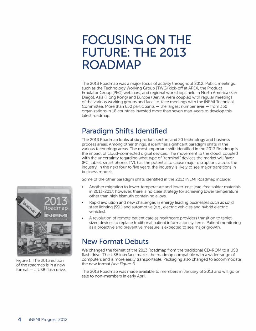
New Format debutsWe changed the format of the 2013 Roadmap from the traditional CD-ROM to a USB flash drive. The USB interface makes the roadmap compatible with a wider range of computers and is more easily transportable. Packaging also changed to accommodate the new format (see Figure 1).
The 2013 Roadmap was made available to members in January of 2013 and will go on sale to non-members in early April.
Figure 1. The 2013 edition of the roadmap is in a new format — a USB flash drive.

Advancing manufacturing technology 5
SETTING THE 2013 COllABORATION AGENdAWe significantly broadened our agenda and areas of collaborative development work during 2012, and identified new initiatives for 2013 and beyond. We completed 10 projects during the year, some of which were two and three-year, multi-phased efforts that wrapped up this year. We ended 2012 with 11 projects launched, three in sign-up, six in development and eight new areas of collaboration targeted for 2013.
Several of the new projects launched this year took us into areas where we have not worked previously. For example, two MEMS initiatives were in sign-up at the end of the year, and a project focused on UL certification was launched mid-year.
New Methodology to Identify Areas of CollaborationiNEMI implemented a new process to actively involve our members in proposing new collaborative R&D projects. This new process led to a list of eight new areas to be pursued in 2013.
The process began by reaching out to members to get inputs on key areas where R&D work was needed. With this input, we developed a list of 23 potential initiatives that covered ten different areas. We then surveyed our members to determine where the majority of their interests lay and to pick the highest priority projects to drive forward. The survey narrowed the list down to eight topics (see below). Formation teams will begin organizing in the first quarter of 2013 to pursue these projects. There are 35-45 companies interested in participating in each of these new initiatives.
We need to ensure that we have critical mass and appropriate leadership in
projects we take forward. As an organization, we only
have so many resources and need to pick the right projects – ones that have the greatest support from
our members and will have the most impact.
Bill Bader, iNEMI CEO
pROjECT AREAS IdENTIFIEd
FOR 2013
1. Address key technology challenges and measurement capabilities needed to deliver ultra-low-loss, high-reliability PCB laminate and board performance.
2. PCB surface finish evaluations by market segment (goal: reduce options).
3. Board assembly and/or test equipment utilization optimization; specifically focused on factories with high mix and large numbers of changeovers.
4. Rework – high-reliability challenges on high-density PCBs, ultra-small components, and maximum number/type of rework cycles.
5. Do the necessary development and studies to demonstrate acceptable reliability performance of copper wire bonding in conjunction with low CTE, halogen-free mold compounds.
6. Develop a stakeholder-aligned methodology/stepwise approach to develop and assess new or alternative materials.
7. Identify and communicate/share best known practices for recycling, metals recovery, and resource efficiency at end-of-life processing.
8. Eco-design for recycling/sustainability including toxicity assessment and critical usage/application: create a quantifiable set of metrics and potentially a tool for measuring a product’s true recyclability and reuse.

6 iNEMI Progress 2012
BROAdENING OuR pROjECT pORTFOlIO2012 was the most active year ever in terms of new project development. We launched 11 new projects and, at the end of the year, had three projects in sign-up and six in development. Some of the new projects took us into areas where we have not worked before, such as MEMS (microelectromechanical systems).
launched in 2012Counterfeit Components project, phase 1 (Assessment Methodology and Metric development) Leader: Colm Nolan (IBM)
The concept of counterfeit electronic components and materials is not a new phenomenon. However, global trade of counterfeit components has recently increased markedly. Counterfeit components can be produced, sourced, and distributed in many different ways, and the identity of these non-standard parts is usually well concealed in the supply chain. Phase 1 of the Counterfeit Components Project will develop assessment methodologies with associated metrics to assess the overall extent of the counterfeit problem in the electronics industry. The outputs will enable iNEMI members to assess the risk of counterfeit use in their respective industries, the risk of untrusted sources of supply in that industry and understand the total cost of ownership associated with those risks.
Board Flexure Standardization, phase 3 (Manufacturing Strain Guidance for pb-Free pCBAs) Leaders: Jagadeesh Radhakrishnan (Intel) and Matt Kelly (IBM)
Based on recommendations and input from the iNEMI Board Flexure Standardization Project, IPC updated its standard, IPC-9704, IPC/JEDEC Printed Wiring Board Strain Gage Test Guideline, in February 2012 to encompass the impact of Pb-free electronics and incorporate consistent strain gage placement/measurement techniques to monitor printed circuit board assembly (PCBA) flexure within a manufacturing environment. However, the resulting IPC-9704A did not include the original Appendices A and B, which outlined strain limits and provided reference for rate-limited strain guidance for eutectic solder. Phase 3 of the Board Flexure Standardization Project will develop a white paper that provides the Pb-free content additions that would have been provided in the deleted appendices.
packaging Equipment Convergence Requirements Leader: Jeffrey S. Pettinato (Intel)
This project’s goal is to create uniform industry requirements for packaging equipment in the areas of: (1) equipment software automation, (2) equipment electro-static discharge (ESD) capabilities and test methods, (3) material handling systems capabilities and test methods, and (4) conservation efforts to reduce consumption (power, water, gas, etc.) and emissions (waste). It will align the industry on a common set of requirements, define and publish instrumentation specifications and methods to validate equipment requirements, and classify which types of equipment require which standards to provide clarity to equipment suppliers.
Board Assembly
Figure 2. New board assembly projects address counterfeit components, requirements for packaging equipment and PCBA reliability requirements.

Advancing manufacturing technology 7
pCBA Reliability Qualification Leaders: Thomas Homorodi (Dell) and Aamir Kazi (Dell)
The proliferation of industry standards and procedures to assess and test the quality and reliability of electronic soldered assemblies (PCBAs) means that the product reliability qualification results of any given manufacturer are not easily correlated with their peers’ results or with OEM expectations. This project proposes to develop a standardized reliability qualification procedure for PCBAs intended for use in enterprise products. Utilizing existing industry specifications for acceptability and testing, the project plans to establish a common hardware reliability qualification process for computing hardware (servers, storage and switches) to be deployed in offices, datacenters and environmentally controlled telecom datacenters.
Reliability Requirements for Implantable Medical devices Leaders: John McNulty (Exponent Failure Analysis Associates, Inc.) and Erik Jung (Medical Microsystems)
FDA clearance procedure calls for manufacturers to provide a full risk analysis and trace issues for their products’ operations. However, the FDA evaluators rely on data derived from existing harsh environment standards and on manufacturers’ own expertise, and neither of these risk management strategies foresees the issues specific to implantable electronic devices. While there are already standards in place to counter this situation for a number of medical devices and systems, no general set of test standards exists for implantable devices. Standardization of recurring scenarios and their application to test routines will mitigate risk factors and offer a faster level of innovation, while delivering reliable products to patients. This recently launched project will attempt to achieve this target by (1) reviewing reliability standards relevant to implantable medical electronic devices, (2) analyzing gaps and developing protocols, and (3) recommending methodologies.
Qualification Methods for portable Medical products Leaders: Grady White (NIST) and Jack Zhu (Boston Scientific)
This project is developing a reliability qualification method for portable electronic medical equipment. Portable medical devices are products such as patient monitoring systems that are used to measure and monitor patients’ vital signs and other bodily functions, including home diagnostics products (e.g., blood pressure cuffs, blood glucose meters, pulse oximeters and biochemical analysis meters) and the peripheral products of implantable medical systems (e.g., external chargers and remote controls). This project will identify current best practices in assessing reliability of portable electronic devices, identify procedures that can be applied to these type devices, identify any gaps in those procedures, and develop a set of procedures acceptable to the medical electronics industry.
Component Specifications for Medical products Leaders: Diganta Das (CALCE-UMD) and Peter Lampacher (Vibrant MED-EL)
This project is working to develop a test and screen matrix for electronic components that can be used to qualify their reliability for implantable and wearable electronic medical devices. These tests and screens will be identified from relevant existing test methodologies and standards available in the electronics industry at large. The goal is to develop specifications that can be accepted by device OEMs as well as supported by component suppliers, and that medical device manufacturers can implement within their component management processes. When critical defects and failure mechanisms or test methodologies are already known, the implementation process will be easier. For situations in which the failure mechanisms or test methodologies are not known, this project will be part of a more complex solution.
Medical Electronics
Figure 3. Portable equipment and implantable devices are the
focus of new medical electronics projects.

8 iNEMI Progress 2012
Structural Test of External Memory devices (Boundary Scan Adoption, phase 2)Leaders: Phil Geiger (Dell) and Steve Butkovich (Cisco)
Phase 2 of the Boundary Scan Adoption Project was launched and completed within 2012. This project focused on structural test of external memory devices. The project team evaluated current and upcoming boundary scan-related test methods and DFT (design-for-test) technology solutions, outlining the “pros” and “cons” of each. The project also identified current and future best practices using combinations of test methods and DFT technologies. For a more complete discussion, see page 16.
BIST project, phase 3 (Short-Term and long-Term Strategies for use Case Classification) Leaders: Zoe Conroy (Cisco) and Al Crouch (Asset-InterTech)
The Built-In Self-Test (BIST) Program focuses on the study of “chip” BIST and its promotion for board and system-level applications. Phase 2 identified a “use case” for discussion, modeling and development material. It also identified main users of board BIST plus defined board BIST and its “value add.” The use cases identified in Phase 2 — the ability to test the interfaces between two adjacent ASICs and from an ASIC to external memory interfaces — are the focus for Phase 3 work.
warpage Characteristics of Organic packagesLeaders: Wei Keat Loh (Intel), Ron Kulterman (Flextronics) and Richard Coyle (Alcatel-Lucent)
This project was organized to identify primary factors that can contribute to warpage of selected components during typical SMT processes. Current qualification criteria and standards are not adequate to predict good yield results at first- and second-level assemblies, and measurement methods (dimensional and test) are neither common nor up-to-date. This team is defining a qualification method and a set of criteria (e.g., sample size, precondition, variations of material and processes at the first and second levels), which could be used to evaluate warpage characteristics of new and existing packages in the design and manufacture of products. The objective is to better understand package warpage characteristics across different package types and attributes. The work will incorporate an evaluation of how to improve package warpage qualification processes plus will benchmark (i.e., “fingerprint”) package warpage characteristics and identify best-in-class measurement methods/protocols. This effort will provide a piece of a large complex problem, the results of which may be used as a stepping stone for future projects.
Improving ul Certification of laminates and pCBs Project leaders: Jackie Adams (IBM), Greg Monty (Underwriters Laboratories) and Valerie St.Cyr (Teradyne)
Technology advancements in PCB materials and densities have progressed at a very rapid rate. Low-halogen laminates, HDI materials, and inks and pastes that embed functions or connection structures are increasingly common. Existing UL certification requirements need to be updated to support these new PCB designs and to streamline the certification process. iNEMI organized this project to develop clear, well-defined recommendations to improve current UL materials and PCB standards. Planned as a two-phase effort, the project will evaluate UL’s existing laminate and PCB certification process, assessing whether new materials, processes and other variations are being adequately addressed, and — where they are not being addressed — recommend use of alternative (existing) testing or development of new tests. The team will also identify ways to shorten the time required to acquire UL certification.
Test Technology
packaging Technology
Organic pCB
Figure 5. Project will update and improve UL certification process.
Figure 4. Phase 2 of the Boundary Scan Adoption Project addressed structural test of external memory devices.

Advancing manufacturing technology 9
In Sign-up
MEMS Reliability Methodologies
One of two new MEMS projects, this effort will focus on reliability testing requirements for inertial MEMS devices, which include accelerometers and gyroscopes. The team will compile end use environments, or “mission profiles,” for a range of applications and perform testing to demonstrate reliability in each application. At a minimum, the project plans to include military, medical, handset, gaming, laptop/tablet PC, and automotive, and several other applications could also be considered. The team plans to solicit opinions of users, designers and manufacturers to develop consensus guidelines for the disposition and reporting requirements for qualification rejects.
MEMS Test Methods and Capabilities
The goal of this project is to identify a common set of practices to improve communication among device manufacturers and their customers. It will include the collection of performance specifications reported in device data sheets for various manufacturers and the identification of opportunities and needs (or gaps) to create common practices. The project will focus on inertial sensors, including MEMS accelerometers and gyroscopes, and on inertial measurement units (IMUs). It will identify what specifications (performance metrics) are reported in publicly available datasheets, how the specifications are defined, identify test methods and protocols used to measure the performance metrics, and determine what units are used. Analysis of this information will determine the level of consistency in the industry and identify opportunities to develop a uniform set of agreed-upon industry tests and terminology for specifying device performance in data sheets. The results of this study will be used in consideration of other projects.
Advanced Si-Node pb-Free underfill Reliability, phase 2
This project is a continuation of the Advanced Si-Node Pb-Free Underfill Reliability Project. In Phase 1, the project team surveyed industry regarding concerns about underfill performance and reliability. Survey results were summarized and published to all iNEMI member companies. Survey findings and published literature indicated that advanced Si-node flip chip components may see operating conditions where silicon Tj approaches underfill Tg. These components may pass standard JEDEC temperature cycling but fail in the field as a result of power cycling and some combination of transitional underfill thermal mechanical properties. Phase 2 will evaluate the performance of a standard temperature cycle test routine against an experimental routine that will be tailored to more closely approximate the actual temperature conditions experienced by a device in a high duty cycle environment.
Figure 6. Shown here is a MEMS accelerometer device.
10 iNEMI Progress 2012
dElIvERING RESulTS We completed several projects this year, some of which were multi-phased projects that had run for several years, while others were projects that both began and ended in 2012, as described below.
A Simplified Tool for Evaluating Environmental ImpactEco-Impact Evaluator for ICT Equipment project, phase 2 Leaders: Tom Okrasinski (Alcatel-Lucent) and John Malian (Cisco)
Providing eco-impact analysis of ICT (information and communication technology) products is a rapidly increasing requirement for placing these products on the market. Measuring environmental impact is important for the industry to demonstrate action in assessing and reducing its carbon footprint.
iNEMI’s Eco-Impact Evaluator for ICT Equipment Project has developed a framework and a simplified proof-of-concept tool for estimating environmental impact of ICT equipment that will allow companies to more quickly and easily evaluate and optimize design trade-offs. Such a tool can aid in early design-for-environment processes that can be embedded into a company’s product life cycle.
develop Simplified Tool
In Phase 2 (completed Q3 2012), the project developed a modular foundation and a viable proof-of-concept tool. The result was a spreadsheet-based software tool that can be used by a product designer or environmental life cycle assessment (LCA) practitioner to estimate the greenhouse gas emissions for an ICT product over its life cycle stages.
Data that was aggregated to produce the tool’s supporting database and algorithms was compiled from currently available information and LCA datasets. The project team also initiated data collection and updates for key areas in the environmental impact estimator: bare printed wiring boards, large ICs, displays, product final assembly and test.
Several project participants completed testing of the tool for an external project. They compared it to traditional detailed life cycle environmental impact assessment using software such as GaBi and SimaPro and found it to be within 5% of the results.
For us, taking something that might normally require 10 to 20 hours to complete and getting it down to half an hour or an hour is a huge deal.
John Malian, Sustainability Engineer, Cisco
Alcatel-Lucent puts carbon footprint data into our product eco-declarations that accompany new product family introductions.
iNEMI’s Eco-Impact Evaluator methodology is the foundation for our tools, which we have now developed into web-based tools that provide key eco-impact information for our product developers. Designers can choose different components and subassemblies
that have already been analyzed and stored in our database. They can then use them as building blocks, choosing the ones that are more energy-efficient and less carbon-intensive. It allows designers to do ‘what-ifs’ and build out the product in a more eco-sustainable way.
Tom Okrasinski, Bell Labs CTO Environmental Engineering, Alcatel-Lucent
BuIldING ECO‑SuSTAINABlE pROduCTS

Advancing manufacturing technology 11
The team recognized that possible merging of work activities and data with other external groups, such as PAIA (Product Attribute to Impact Algorithm, a collaborative MIT Project), could offer significant benefits in developing a combined data set and tool for enhanced and more widespread use by the ICT industry. As a follow-on, groups such as iNEMI, PAIA and EICC (Electronic Industry Citizenship Coalition) are beginning to collaborate on collecting and updating environmental impact data for ICT components.
Further data collection and refresh should be made at an industry average level, which will greatly help in collecting data across the ICT industry where transparency will be very important. An example of this would be using the Semiconductor Industry Association’s (SIA’s) data averaged for integrated circuit manufacturing, which this industry association maintains and regularly updates.
iNEMI is having ongoing discussions to identify a hosting organization that can continue to maintain and update the tools developed by the project team.
project demonstrates performance of HFR-Free Materials and Supply Chain ReadinessHFR-Free pCB Materials, phase 2 Leader: John Davignon (Intel)
iNEMI organized the HFR-Free PCB Materials Project in 2009 to evaluate and direct the technology readiness, supply chain capability, and reliability characteristics for HFR-free printed circuit board materials and assemblies. The two-phased effort, part of iNEMI’s HFR-Free Leadership Program, was completed in early 2012.
In 2009, many OEMs/ODMs were looking for alternatives to halogenated flame retardants (HFRs), in particular, to replace brominated flame retardants. Many companies set their own transition dates to move to HFR-free technology, which created some confusion in the supply chain since these dates varied by company. In addition, there were many unknowns and concerns about HFR-free materials, including questions about loss of performance (compared to FR4 laminates); problems with high-speed bus designs due to electrical properties of HFR-free materials; variations in flame retardants being used, resulting in a wider fluctuation of supplier-to-supplier PCB electrical performance compared to FR4 designs; and concerns about the volume capacity to support widespread transition to HFR-free.
With these concerns in mind, the HFR-Free PCB Materials Project team set the following goals:
1. Identify the technology readiness, supply chain capability, and reliability characteristics for HFR-free alternatives to conventional PCB materials and assemblies (electrical and mechanical properties).
2. Define technology limits for HFR-free materials across all market segments with initial focus on desktop and notebook computers in the 2011 timeframe.
3. Define and implement quantifiable data into the HFR-free laminate suppliers’ datasheets to assist in material selection by users.
4. Define a “test suite methodology” (TSM) that meets the quality and reliability requirements of the chosen market segments.
5. Ensure that industry laminate suppliers have the capability and capacity to support the industry’s HFR-free laminate requirements.
The 18-company project included laminate suppliers, test houses, and OEMs/ODMs, and was divided into two phases. Phase 1 developed the test suite methodology (TSM) and Phase 2 applied the methodology to evaluate HFR-free laminates provided by PCB materials suppliers on the project team.

12 iNEMI Progress 2012
The TSM developed by the project team successfully allows direct comparison of desired laminate properties and can help users compare options and choose the right laminate to replace brominated FR4 in desktop and notebook computers.
The project’s test vehicle modeled a 10-layer notebook construction and developed or modified test coupon designs to match this construction. The TSM was evaluated using six HFR-free laminates with three brominated FR4 laminates as the baseline.
Overall, the program concluded that the electronics industry is ready to transition to HFR-free PCB materials, and that the key electrical and thermo-mechanical properties of the new HFR-free laminates can meet the required criteria. Furthermore, the team verified that existing laminate suppliers could meet the capacity demands for new HFR-free laminates.
HFR-Free Materials Outperform FR4 for Reliability HFR-Free High-Reliability pCB Leaders: Stephen Tisdale (Intel) and Gary Long (Intel)
The European Union’s Restriction on the use of certain Hazardous Substances (RoHS) Directive prohibits the use of polybrominated biphenyls (PBBs) and polybrominated diphenyl ethers (PBDEs) in nonexempt electronic equipment. These compounds can be used as flame retardants, and some of these substances have been shown to present unacceptable risks to human health and the environment. Although PBBs and PBDEs are typically not used in circuit board materials, stakeholders are taking a precautionary stance on the use of other non-regulated halogenated organic substances, such as brominated epoxies for circuit board applications, and are preemptively restricting the use of halogens in their products.
iNEMI organized the HFR-Free High-Reliability Project in 2008 to determine the availability of HFR-free materials and assess their ability to support high-reliability applications in accordance with existing halogenated laminates.
This collaborative team, consisting of OEMs, printed circuit laminate suppliers and electronics manufacturing companies, selected, evaluated and tested a subset of available HFR-free laminates to establish baseline performance knowledge of these materials. The team specifically focused on the requirements for the high-reliability server market with the objective of assessing performance of HFR-free alternatives for printed wiring boards and printed wiring board assemblies.
Test results from this study were used to establish a database for HFR-free laminate material properties that allows for comparison to existing materials, while also demonstrating support for high-reliability products. The team is currently evaluating options to make the database available to the industry at large, allowing for baseline comparison of HFR-free laminate material.
HFR-Free Materials Outperform Counterparts
The main take-away from the team’s testing effort was that HFR-free laminates, in many cases, out-performed their halogenated counterparts. The data demonstrated that HFR-free laminates are available and well suited for today’s higher-reliability products/applications.
The brominated FR4 was in the bottom category in the following seven (out of 10) tests performed: IST (interconnect stress test), CAF (conductive anodic filament), flex modulus, flex strength, CTE (coefficient of thermal expansion), Df (loss tangent), and HATS (highly accelerated thermal stress).

Advancing manufacturing technology 13
In fact, there was no test in which the brominated FR4 performed the best. Moreover, three tests in which the brominated FR4 performed poorly are commonly used reliability tests (IST, CAF and HATS). Since the brominated FR4 laminate is a widely used, well-regarded common material, the team concluded that HFR-free can be more reliable than brominated FR4, depending on the specific application.
Any OEM intending to use HFR-free materials will need to do in-house performance testing because there is no “drop-in” solution readily available. HFR-free laminate candidate choices need to be vetted for optimal performance for a given application. However, the database created by this project will assist in reducing the initial search for HFR-free laminate performance information as compared to existing materials.
determining the Impact of Surface Finishes on pb-Free Solder joint Reliabilitypb-Free Component and Board Finish Reliability projectLeaders: Qinglei Zhang (Intel) and Richard Coyle (Alcatel-Lucent)
The use of Pb-free solder alloys raises concerns regarding solder joint reliability, and these concerns are compounded by the implementation of alternative surface finishes for circuit boards and package substrates/leadframes. Although multiple studies have investigated the impact of Pb-free solder on board-level temperature cycling lifetime, few efforts have dealt with the impact of alternative surface finishes on Pb-free solder joint reliability. iNEMI launched the Pb-Free Component and Board Finish Reliability Project in August 2008 to evaluate the effects of several alternative finishes.
The four-year effort conducted comparative reliability testing on Pb-free components assembled on test boards. The team used mechanical testing, consisting of 4-point monotonic bend testing (IPC/JEDEC-9702) and shock testing, conducted with and without aging.
Test board assemblies were configured to evaluate multiple component surface finishes and two board finishes. The component surface finishes evaluated were: electroless Ni/Au (ENIG), organic solderability preservative (OSP), immersion SN, matte SnNi, and DSOP-SAC paste. The two PWB surface finishes were electrolytic NiAu (note that the sample size was reduced due to manufacturing flaws on these samples), and OSP SAC 305 was used as the solder.
The thing that surprised the entire project team was that all of the materials we tested were as good as, or better than, the brominated flame retardant material across the board. Typically, you would find only half of the materials tested as good or better; this time it was all of the materials tested. This is the third iteration of iNEMI’s low-halogen programs and, by working with suppliers in these projects, they’ve been able to improve their material sets based on parameters that the project teams identified as potential issues. We have also seen availability of materials increase, so there should not be any production problems. The volume of HFR-free laminates sold has more than doubled from 2008 to today.
The majority of companies participating in the project have made commitments to move toward HFR-free, but had little data to say ‘this material is good for those applications.’ Now that we have completed this evaluation, companies can understand there’s not just one or two, but a multitude of materials from which to choose and to move in the direction of HFR-free materials.
Stephen Tisdale Manager, Industry Standards Corporate Product Regulations & Standards Intel Corporation
iNEMI EFFORTS HElp BuIld
Supply CHAIN

14 iNEMI Progress 2012
Key learnings & Results
Acceleration data showed a difference in response between package center and corner, although no effect from surface finish was seen.
Neither interfacial separation nor pad cratering was observed at component side after shock test for all of the component and board surface finishes investigated within the scope of shock test.
Failure on OSP boards was predominantly due to pad cratering.
Electrolytic NiAu boards show a mixed failure mode of intermetallic/Ni interfacial separation and pad cratering, indicating that the intermetallic compound failure point and resin failure point are similar.
Eliminating Creep Corrosion to Reduce pCB Failures Creep Corrosion project, phase 3 Leaders: Xiaodong Jiang (Alcatel-Lucent), Mason Hu (Cisco), and Simon Lee (Dow Chemical)
Creep corrosion is a process in which solid corrosion products (typically sulfide and chloride) migrate over a surface without the influence of an electrical field. Creep corrosion is highly surface-specific and a given corrosion product can only migrate on a specific type of surface. Commonly seen in polluted environments rich in sulfur, this kind of corrosion has predominantly been observed on printed circuit boards with lead-free surface finishes such as ImAg and OSP. In these cases, the corrosion product (typically copper sulfide) “creeps” onto the solder mask surface and causes short circuits between adjacent pads and traces. Creep corrosion on printed circuit boards is promoted by the residue of certain types of fluxes, and is affected by temperature and humidity in the environments.
Although corrosion of electronics is a significant issue, there has been little agreement on the test methods and conditions that should be used to simulate the environmental conditions and predict potential failures. Development of a corrosion test is necessary to qualify products that can survive harsh environment.
iNEMI launched the multi-phased Creep Corrosion Project (Q4 2009) to investigate factors influencing creep corrosion and formulate methods for mitigating the problem. In Phase 1, the project team collected data on creep corrosion failures and related factors, and then analyzed the output in Phase 2, narrowing down the major factors that influence creep corrosion.
Testing Expands Industry Knowledge
Phase 3 (completed Q4 2012) performed laboratory-based experiments to further investigate the sensitivities of the influencing factors, including surface finish, flux, solder mask geometry, solder paste coverage, reflow and wave soldering, and mixed flowing gas (MFG) test conditions (corrosive gas concentration, humidity, temperature).
ImAg, OSP, Pb-free HASL, ENIG and ImSn finished boards with Pb-free solder paste reflowed on the top side and wave soldered on the bottom side — some with no-clean organic acid flux and others with no-clean rosin flux — were subjected to MFG environments with gaseous composition adjusted to achieve the targeted 500-600 nm/day copper corrosion rate.
Testing results were clear — the presence of organic acid flux for wave soldering applications accelerated the formation of creep corrosion products across all surface
Figure 7. ENIG with organic acid flux showed high levels of creep corrosion after 20 days MFG.

Advancing manufacturing technology 15
finishes. An accelerated corrosion testing based on modified MFG conditions rich in hydrogen sulfide gas was shown to trigger creep corrosion across multiple PCB surface finishes. This corrosion in general was dependent on the surface cleanliness. Contamination on the PCBA in the form of flux residues when using organic acid fluxes for soldering applications can cause corrosion across most surface finishes. Rosin-based, low activity, no-clean fluxes seem to be less prone to creep corrosion. Likewise Pb-free HASL and ImSn based PCBs experienced less creep corrosion.
The response of various surface finishes to MFG test conditions was interesting. Earlier studies on ImAg and OSP with organic acid fluxes clearly demonstrated the limitations of these surface finishes when used with organic fluxes. This latest work agrees with these findings; however, a new finding is the marginality of ENIG surface finish. It is unclear at this point if it is related to the quality of the PCB (thickness of Au, porosity). As expected, the Pb-free HASL and ImSn did show good creep corrosion resistance. Tin is more anodic with respect to copper than gold is on ENIG. Moreover, low reactivity of Sn-based alloys in sulfide-rich environments suggests the stability of these surface finishes to withstand corrosive elements.
The project team validated the effectiveness of a few mitigation approaches and correlated experimental test conditions to environment classification standards. They issued a position statement (June 6, 2012) that provided the electronics industry with guidelines for avoiding creep corrosion on printed circuit boards in data centers and telecommunication rooms (see below).
Next Steps
At the end of 2012, a new project was proposed to develop a cost-effective and reliable creep corrosion qualification test that PCB, component and material suppliers can use to satisfy their customers that their products will not creep corrode in the field, especially in geographies polluted with sulfur-bearing gaseous contamination. Initial work will focus on flowers of sulfur testing.
Environmental corrosion of electronics is a complex
area of research. iNEMI should be credited for
bringing together scientists and engineers at various
companies to focus on this issue, share their findings
and identify the biggest technical gaps that need to
be addressed.
Anil Kurella, senior failure analysis engineer (Intel
Corporation) and a member of the Creep
Corrosion Project team
The Creep Corrosion Project published a position paper outlining limits of temperature, humidity and gaseous contamination in data centers and telecommunication rooms to avoid creep corrosion on printed circuit boards.
This position statement defines the temperature, humidity and copper and silver corrosion rate limits within which PCBs will perform reliably in the field with respect to creep corrosion. Existing studies indicate that the most effective way to protect electronic hardware from creep corrosion is to ensure that environmental conditions are within the modified severity level G1 of ANSI/ISA-71.04-1985, Environmental Conditions
for Process Measurement and Control Systems: Airborne Contaminants (ISA 1985):
• A copper reactivity rate of less than 30 nm/month
• A silver reactivity rate of less than 20 nm/month
The recommended ranges for temperature and humidity are based on white papers from the American Society of Heating, Refrigerating and Air-Conditioning Engineers (ASHRAE):
• Temperature within 18° to 27°C
• Relative humidity less than 60%
• Dew point within the range of 5.5° to 15°C
iNEMI pROvIdES GuIdElINES TO
AvOId CREEp CORROSION

16 iNEMI Progress 2012
Boundary Scan Team Tackles Testing of External Memory devicesStructural Test of External Memory devices (Boundary Scan Adoption, phase 2)Leaders: Phil Geiger (Dell) and Steve Butkovich (Cisco)
Phase 1 of the Boundary Scan Adoption Project (completed Q4 2009) surveyed board and system engineers, along with semiconductor engineers, to gauge the penetration of boundary scan implementation within the electronics manufacturing industry. The survey sought to identify any barriers to implementation.
One of the key gaps identified by the survey was that more than 80% of board test engineers were struggling to implement boundary scan-based connectivity testing on soldered down SRAM/DRAM memory devices with no on-chip testability (excluding DIMMs and other plug-in memory). As a result, the team concluded that structural connectivity test of external memory devices was a “crisis in waiting” as memory devices get larger and faster.
Phase 2 of the Boundary Scan Project focused on structural test of external memory devices. The project team evaluated current and upcoming boundary scan-related test methods and DFT (design-for-test) technology solutions, outlining the “pros” and “cons” of each. The project also identified current and future best practices using combinations of test methods and DFT technologies.
Overall, the project team found that board-level testability in memory devices was almost non-existent. No “test mode” is unilaterally designed into memory devices to allow easy, straightforward generation of a structural test. Without a comprehensive structural test to find and diagnose failures, functional board test (FT) must take up the slack, which can cause assembly and test costs to increase. FT development, debug and repair processes become much more complex, and additional FT development is required to ensure test coverage (i.e., more extensive memory test development). There is significant reduction in test failure diagnosis. Additional FT stations are required for production and debug/repair. All of these factors lead to higher capital equipment, operator and maintenance costs.
Best practices Identified
In the near future (2015), new DFT techniques will begin to come into play and, by 2018, new DFT techniques could be mainstream, enabling more solutions. Best practices for 2012 included powered opens (without IEEE 1149.8.1), ICT (in-circuit test), integrated boundary scan and stand-alone boundary scan.
By 2015, best practices are also expected to include IEEE 1581 and JEDEC scan-enabled technologies. These practices will likely continue into 2018.
Future Steps
At the end of 2012, planning was under way for Phase 3 of the Boundary Scan Adoption Project, which will do a follow-up industry survey to determine whether boundary scan-related issues have decreased since the original survey, identify what old issues are still around, what new issues have come up, and gauge the industry’s awareness of the upcoming changes to 1149.1 .bsdl files.
Figure 8. Board test engineers are struggling to implement boundary scan-based connectivity testing on soldered down SRAM/DRAM memory devices.

Advancing manufacturing technology 17
iNEMI Asks Industry about wiring density Needs
wiring density for Organic packaging Substrates project
Meeting the wiring density needs of the next generation of packaging technology will require improvements in all areas of organic packaging substrates technology; a piecemeal approach will not be sufficient.
iNEMI’s Wiring Density for Organic Packaging Substrates Project surveyed the industry on current wiring density, design rule capabilities and future requirements. Their goal was to get industry feedback on which substrate design features should be included in future collaborative work to effectively address wiring density needs from the perspective of material set, low-cost lithography/laser, plating, and inspection and test. The questionnaire covered the following categories:
• Driving forces for higher-density package and configuration.
• Devices requiring high-density substrates.
• Capability and future anticipated needs for flip chip pad pitch, line space per dielectric thickness, via diameter and aspect ratio.
• Materials for dielectrics.
• Process technologies for photoresist exposure, blind via and buried via formation, and copper plating.
• Layer-to-layer alignment of dielectrics and solder masks.
It also looked at the impacts of Si architecture, package architecture and substrate process capabilities on wiring density.
According to survey respondents, the preferred options to increase wiring density are (in order): (1) shrink via capture pad, (2) decrease lines and spacing size and pitch and (3) add layers.
Alternative methods (ranked below the three preferred options) included: embedded die technology, novel routing schemes, improved die and package design (co-optimization), higher-speed, inter-chip communication protocols to reduce signal trace count, and silicon and glass interposers.
Gaps Identified
While technology exists to meet the roadmap, the indication is that the technology is not cost-efficient. The industry is approaching the point in several areas where current technology and equipment starts to be too costly if requirements are tightened further. New and novel technologies that are cost-efficient are needed.
Numerous process steps that affect yield were identified as requiring attention, such as build-up layer application and circuit imaging. Other areas included decreasing capture pad size track, finer tracks, adding layers, and improving test capability at substrate suppliers and after packaging is completed.
Since survey respondents did not deem any single step as the most critical, the team recommended that a “holistic” optimization is necessary and that industry sectors need to work together to enable finer bump pitch and higher substrate wiring density.
Figure 9. When asked about the most practical way to increase substrate density, the majority of survey respondents said to
decrease line and space width.

18 iNEMI Progress 2012
project develops Method to Measure Separation Gap for Optoelectronic ConnectorsConnector particle Thickness Investigation project, phase 1Chair: Tatiana Berdinskikh (Celestica)
This project was organized to investigate the impact of particles thickness on connector optical performance. Previous work had suggested that connector separation caused by particles on the cladding and/or ferrule impacts signal performance. Quantitative measurements of this phenomenon, however, had not been completed. Previous efforts found it difficult to measure the separation of the mated connectors.
For this experiment, the project team purposely introduced contamination on the end-faces of fiber optic connectors, mated them, measured optical performance and recorded images of the end-faces. Using a confocal-type microscope, the team measured article height to understand the upper limit on fiber separation due to the particles. They then related the resultant optical performance to the theoretical Fabry-Perot effects due to fiber separation for each of four wavelengths (1310, 1490, 1550 and 1625nm).
Controlled Separation Experiment
The project team successfully performed a controlled separation experiment to verify the ability of a multiple wavelength probe, using existing test equipment, to measure the mated connector separation gap. Controlled separation was used to map signal performance as a function of gap for multiple wavelengths from full contact to several microns of gap between ferrule end-faces.
The experiment demonstrated that a multiple wavelength interrogation technique could be used to probe the separation distance in a mated connector.
New Contamination Technique
The project team developed a novel contamination technique allowing them to contaminate a cladding and ferrule while maintaining a clean fiber core. They used three types of contaminants: Arizona dust, silver particles and toner particles.
project Conclusions
The project completed a foundational experiment to determine the performance limits of a multiple wavelength interrogation technique for determining mated connector separation distance from contact to tens of microns of separation. The team developed methods for controlled contamination of samples in a manner appropriate for investigation of connector separation without blocking the core. They also developed methods for measuring particle thickness in unmated conditions using a confocal microscope (see Figure 10).
Next Steps
A new project is being proposed to develop a cleanliness specification for lens-based optical transceivers and connectors.
Figure 10. Top: Confocal microscope photo simulation view of end-face contaminated with silver particles. Bottom: Photo simulation view after the fifth mating. Transfer occurred after first mating and now appears to cover the fiber core.

Advancing manufacturing technology 19
Team Identifies Reliability Risks with New devices & underfill; Second phase planned to EvaluateAdvanced Si-Node pb-Free underfill Reliability Leader: Robert Carson (Cisco)
This project was organized to determine whether gaps exist in temperature cycle testing standards that may result in long-term reliability issues for some high duty cycle devices using advanced Si-nodes. The material challenges created by advanced silicone node devices, coupled with Pb-free packaging requirements, have created a situation where the long-term reliability determined by standard temperature cycle testing should reasonably be called into question and reviewed.
The cost and performance requirements for current IC (integrated circuit) designs have been driving silicon processing to finer process nodes. The finer nodes along with Pb-free packaging requirements have created unique thermal-mechanical issues and brought the packaging material properties and their long-term reliability into focus. As the silicon node is miniaturized, there is increased current leakage, which acts to raise device operating temperature. The requirement for Pb-free bumping further complicates the system by introducing a higher solidification temperature (greater CTE — coefficient of thermal expansion— mismatch between die and substrate) and lower ductility in the interconnect alloy.
Historically, flip chip underfill has alleviated many of the CTE issues by securing the die and substrate and absorbing thermal-mechanical stresses. These underfills would typically have Tg (glass transition temperature) well in excess of the silicon operating temperature to ensure stable performance throughout product service conditions. Beginning with the introduction of ELK dielectrics and requirements for Pb-free bumps, designers have encountered conditions where high Tg underfill has been a source of ELK dielectric cracking and have begun using underfills with progressively lower Tg to reduce the dielectric stresses.
As Tj approaches the underfill Tg, flip chip stress distribution changes radically, as shown in Figure 11. At temperatures between underfill Tg and substrate Tg, all the silicon/substrate CTE mismatch and warpage stress is carried through the bump structure and the fragile silicon ELK layers. For high-performance applications with increasing silicon operating temperature, such as gaming ICs, broadband switches and routers, the shrinking gap between Tg and Tj creates the potential for unstable stress conditions.
Historically, the thermal-mechanical stability of the flip chip system has been evaluated using standard temperature cycling tests; however, that was when underfill Tg was higher than the temperature cycle maximum. Furthermore, the typical operating conditions for some advanced Si-node ICs have made possible numerous transitions through the underfill Tg and may, in effect, exceed the operating conditions originally conceived by the reliability test.
Phase 1 of the Advanced Si-Node Pb-Free Underfill Reliability Project conducted a survey to identify industry-wide concerns about underfill performance and reliability. Based on the findings from this survey, along with a review of published literature and standard practices related to the selection of underfill material properties, the team determined that advanced Si-node flip chip components may see operating conditions where silicon Tj approaches underfill Tg. These components may pass standard JEDEC temperature cycling but fail in the field as a result of power cycling and some combination of transitional underfill thermal mechanical properties.
The team’s investigations provided the information necessary to design an experimental test vehicle and develop a testing routine that will be used in the project’s second phase, which was in sign-up by the end of the year.
Issues with Tg~Tj
Tg>Tj Tg<Tj
Uniform Stress Distribution
Stress Concentration at Flip Chip Bumps
Issues with Tg~Tj
Tg>Tj Tg<Tj
Uniform Stress Distribution
Stress Concentration at Flip Chip Bumps
Figure 11. Stress distribution as device Tj approaches underfill Tg.

20 iNEMI Progress 2012
2012 INEMI MEMBERS*
Advanced Semiconductor Engineering Group (ASE)
Agilent Technologies, Inc.
Akrometrix, llC
Alcatel-lucent
Alent
Alpha (Alent)
Amkor Technology
Arizona State university
Assembleón Netherlands**
ASSET InterTech, Inc.
AT&S AG
Atotech
BlackBerry
Boston Scientific CRM
CAlCE (Center for Advanced life Cycle Engineering)**
CBA Group llC
Celestica, Inc.
Center for Innovative Technology (CIT)
Cisco
Cochlear limited**
Compliance & Risks ltd.
Corelis
dell, Inc.
delphi Electronics & Safety
dfR Solutions
doosan Corp. Electro-Materials BG
dow Electronic Materials
dSM Engineering plastics
dyCONEx AG (Micro Systems Technologies)
Elec & Eltek International Company limited
Electronic Components Association (ECA)
Elite Material Co., ltd.
Endicott Interconnect Technologies, Inc. (EIT)
Enthone (Alent)
Exponent, Inc.**
FiberQA llC
Flextronics International
Fraunhofer IZM
Georgia Institute of Technology
Global Innovation Research Center, peking university
Griffith university**
Henkel
Heraeus
Hewlett-packard Company
Hitachi Chemical Co., ltd.**
Hover-davis (CBA Group)
Huawei Technologies Co., ltd.
IBIdEN CO., lTd.
IBM
IEC Electronics**
IHS
imec
Indium Corporation of America
Industrial Technology Research Institute (ITRI)
Integrated Electronics Engineering Center (IEEC), SuNy-Binghamton
Intel Corporation
Inventec performance Chemicals
IpC-Association Connecting Electronics Industries
IST-Integrated Service Technology, Inc.
ITEQ Corporation
ITI (Information Technology Industry Council)
juniper Networks
KxI (Shenzhen Kunqi xinhua Technology Co., ltd.)**
lenovo
linksys (Cisco)
lotes Co. ltd.**
Massachusetts Institute of Technology (MIT)
MEd-El Elektromedizinische Gerate GmbH
MEMS Industry Group
Micro Systems Engineering, Inc. (Micro Systems Technologies)
Micro Systems Technologies
Micronic Mydata AB
Microsoft
Multek (Flextronics)
NAMICS Corporation**
Nan ya plastics Corporation
National Center for Manufacturing Sciences (NCMS)
National Institute of Standards and Technology (NIST)
NGK Spark plug Co., ltd.
Nihon Superior Co., ltd.
Nippon Micrometal Corporation
Nordson Advanced Technology Systems Business Group**
NTK Technologies
OIdA (Optoelectronics Industry development Association)**
pacific Insulating Material Company limited (Elec & Eltek)
pinfa (phosphorus, Inorganic and Nitrogen Flame Retardants Association)
plexus Corp.
purdue university
Rochester Institute of Technology
Samsung Electro-Mechanics Co., ltd.
Sanmina-SCI Corporation
Scientific Atlanta, Inc. (Cisco)
Senju Comtek Corp. (SCC)
Shengyi Technology Co., ltd.
Speedline Technologies, Inc.
STATS ChippAC
Taiwan printed Circuit Association (TpCA)
TE Connectivity
TechAmerica
Teradyne, Inc.
Texas Instruments Incorporated
The vinyl Institute
ul llC
universal Instruments (CBA Group)
university of California at Berkeley
valtronic Technologies**
wistron Corporation**
*As of 12/31/12
**joined iNEMI in 2012
CONTACT uSNorth America
2214 Rock Hill Road Suite 110 Herndon, Virginia 20170-4214 Phone: +1 703-834-0330 Fax: +1 703-834-2735
Asia
The 21st Century Building 6F, Room 6026 210 Century Avenue Pudong, Shanghai 200120 China Phone: +86-21-5172 7275 Fax: +86-21-5172 7276
Europe
Sandville House Friarstown, Grange Kilmallock, Co. Limerick Ireland Phone: +353-87-9040-363 Fax: +353-61-351-935
Internet
www.inemi.org [email protected]


![INDEX [] INDEX Message from the Chairman- Emeritus ..... 02 Message from the Chairman 03](https://static.fdocuments.in/doc/165x107/5ad105637f8b9aca598e53be/index-index-message-from-the-chairman-emeritus-02-message-from-the-chairman.jpg)