RF Power LDMOS Transistorcdn.everythingrf.com/live/659_171_mrfe6vp61k25n_MRFE6VP61K25N.pdf ·...
19
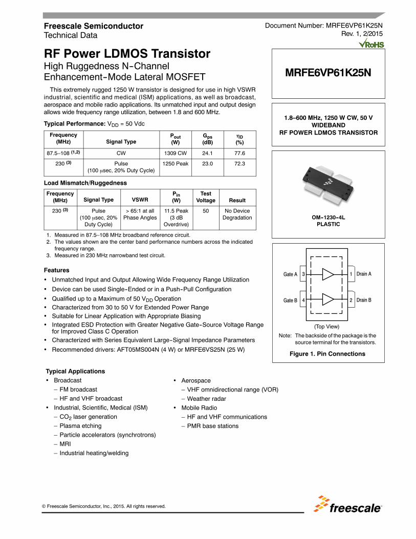
RF Power LDMOS Transistor High Ruggedness N--Channel Enhancement--Mode Lateral MOSFET This extremely rugged 1250 W transistor is designed for use in high VSWR industrial, scientific and medical (ISM) applications, as well as broadcast, aerospace and mobile radio applications. Its unmatched input and output design allows wide frequency range utilization, between 1.8 and 600 MHz. Typical Performance: V DD = 50 Vdc Frequency (MHz) Signal Type P out (W) G ps (dB) D (%) 87.5–108 (1,2) CW 1309 CW 24.1 77.6 230 (3) Pulse (100 sec, 20% Duty Cycle) 1250 Peak 23.0 72.3 Load Mismatch/Ruggedness Frequency (MHz) Signal Type VSWR P in (W) Test Voltage Result 230 (3) Pulse (100 sec, 20% Duty Cycle) > 65:1 at all Phase Angles 11.5 Peak (3 dB Overdrive) 50 No Device Degradation 1. Measured in 87.5–108 MHz broadband reference circuit. 2. The values shown are the center band performance numbers across the indicated frequency range. 3. Measured in 230 MHz narrowband test circuit. Features Unmatched Input and Output Allowing Wide Frequency Range Utilization Device can be used Single--Ended or in a Push--Pull Configuration Qualified up to a Maximum of 50 V DD Operation Characterized from 30 to 50 V for Extended Power Range Suitable for Linear Application with Appropriate Biasing Integrated ESD Protection with Greater Negative Gate--Source Voltage Range for Improved Class C Operation Characterized with Series Equivalent Large--Signal Impedance Parameters Recommended drivers: AFT05MS004N (4 W) or MRFE6VS25N (25 W) Typical Applications Broadcast – FM broadcast – HF and VHF broadcast Industrial, Scientific, Medical (ISM) – CO 2 laser generation – Plasma etching – Particle accelerators (synchrotrons) – MRI – Industrial heating/welding Aerospace – VHF omnidirectional range (VOR) – Weather radar Mobile Radio – HF and VHF communications – PMR base stations Document Number: MRFE6VP61K25N Rev. 1, 2/2015 Freescale Semiconductor Technical Data 1.8–600 MHz, 1250 W CW, 50 V WIDEBAND RF POWER LDMOS TRANSISTOR MRFE6VP61K25N (Top View) Figure 1. Pin Connections Note: The backside of the package is the source terminal for the transistors. OM--1230--4L PLASTIC Drain A 3 1 4 2 Drain B Gate A Gate B Freescale Semiconductor, Inc., 2015. All rights reserved.
Transcript of RF Power LDMOS Transistorcdn.everythingrf.com/live/659_171_mrfe6vp61k25n_MRFE6VP61K25N.pdf ·...
MRFE6VP61K25N
1RF Device DataFreescale Semiconductor, Inc.
RF Power LDMOS TransistorHigh Ruggedness N--ChannelEnhancement--Mode Lateral MOSFETThis extremely rugged 1250 W transistor is designed for use in high VSWR
industrial, scientific and medical (ISM) applications, as well as broadcast,aerospace and mobile radio applications. Its unmatched input and output designallows wide frequency range utilization, between 1.8 and 600 MHz.
Typical Performance: VDD = 50 Vdc
Frequency(MHz) Signal Type
Pout(W)
Gps(dB)
D(%)
87.5–108 (1,2) CW 1309 CW 24.1 77.6
230 (3) Pulse(100 sec, 20% Duty Cycle)
1250 Peak 23.0 72.3
Load Mismatch/Ruggedness
Frequency(MHz) Signal Type VSWR
Pin(W)
TestVoltage Result
230 (3) Pulse(100 sec, 20%Duty Cycle)
> 65:1 at allPhase Angles
11.5 Peak(3 dB
Overdrive)
50 No DeviceDegradation
1. Measured in 87.5–108 MHz broadband reference circuit.2. The values shown are the center band performance numbers across the indicated
frequency range.3. Measured in 230 MHz narrowband test circuit.
Features
Unmatched Input and Output Allowing Wide Frequency Range Utilization
Device can be used Single--Ended or in a Push--Pull Configuration
Qualified up to a Maximum of 50 VDD Operation Characterized from 30 to 50 V for Extended Power Range Suitable for Linear Application with Appropriate Biasing Integrated ESD Protection with Greater Negative Gate--Source Voltage Range
for Improved Class C Operation Characterized with Series Equivalent Large--Signal Impedance Parameters
Recommended drivers: AFT05MS004N (4 W) or MRFE6VS25N (25 W)
Typical Applications Broadcast
– FM broadcast
– HF and VHF broadcast
Industrial, Scientific, Medical (ISM)
– CO2 laser generation
– Plasma etching
– Particle accelerators (synchrotrons)
– MRI
– Industrial heating/welding
Aerospace
– VHF omnidirectional range (VOR)
– Weather radar
Mobile Radio
– HF and VHF communications
– PMR base stations
Document Number: MRFE6VP61K25NRev. 1, 2/2015
Freescale SemiconductorTechnical Data
1.8–600 MHz, 1250 W CW, 50 VWIDEBAND
RF POWER LDMOS TRANSISTOR
MRFE6VP61K25N
(Top View)
Figure 1. Pin Connections
Note: The backside of the package is thesource terminal for the transistors.
OM--1230--4LPLASTIC
Drain A3 1
4 2 Drain B
Gate A
Gate B
Freescale Semiconductor, Inc., 2015. All rights reserved.
2RF Device Data
Freescale Semiconductor, Inc.
MRFE6VP61K25N
Table 1. Ordering Information
Device Tape and Reel Information Package
MRFE6VP61K25NR6 R6 Suffix = 150 Units, 56 mm Tape Width, 13--inch Reel OM--1230--4L
Table 2. Maximum Ratings
Rating Symbol Value Unit
Drain--Source Voltage VDSS –0.5, +133 Vdc
Gate--Source Voltage VGS –6.0, +10 Vdc
Storage Temperature Range Tstg –65 to +150 C
Case Operating Temperature Range TC –40 to +150 C
Operating Junction Temperature Range (1,2) TJ –40 to +225 C
Total Device Dissipation @ TC = 25CDerate above 25C
PD 333316.67
WW/C
Table 3. Thermal Characteristics
Characteristic Symbol Value (2,3) Unit
Thermal Resistance, Junction to CaseCW: Case Temperature 109C, 1250 W CW, 50 Vdc, IDQ(A+B) = 245 mA, 98 MHz
RJC 0.06 C/W
Thermal Impedance, Junction to CasePulse: Case Temperature 74C, 1250 W Peak, 100 sec Pulse Width, 20% Duty Cycle,IDQ(A+B) = 100 mA, 230 MHz
ZJC 0.016 C/W
Table 4. ESD Protection Characteristics
Test Methodology Class
Human Body Model (per JESD22--A114) 2, passes 2500 V
Machine Model (per EIA/JESD22--A115) B, passes 250 V
Charge Device Model (per JESD22--C101) IV, passes 2000 V
Table 5. Moisture Sensitivity Level
Test Methodology Rating Package Peak Temperature Unit
Per JESD22--A113, IPC/JEDEC J--STD--020 3 260 C
Table 6. Electrical Characteristics (TA = 25C unless otherwise noted)
Characteristic Symbol Min Typ Max Unit
Off Characteristics (4)
Gate--Source Leakage Current(VGS = 5 Vdc, VDS = 0 Vdc)
IGSS — — 1 Adc
Drain--Source Breakdown Voltage(VGS = 0 Vdc, ID = 100 mAdc)
V(BR)DSS 133 — — Vdc
Zero Gate Voltage Drain Leakage Current(VDS = 50 Vdc, VGS = 0 Vdc)
IDSS — — 10 Adc
Zero Gate Voltage Drain Leakage Current(VDS = 100 Vdc, VGS = 0 Vdc)
IDSS — — 20 Adc
1. Continuous use at maximum temperature will affect MTTF.2. MTTF calculator available at http://www.freescale.com/rf. Select Software & Tools/Development Tools/Calculators to access MTTF
calculators by product.3. Refer to AN1955, Thermal Measurement Methodology of RF Power Amplifiers. Go to http://www.freescale.com/rf.
Select Documentation/Application Notes -- AN1955.4. Each side of device measured separately. (continued)
MRFE6VP61K25N
3RF Device DataFreescale Semiconductor, Inc.
Table 6. Electrical Characteristics (TA = 25C unless otherwise noted) (continued)
Characteristic Symbol Min Typ Max Unit
On Characteristics
Gate Threshold Voltage (1)
(VDS = 10 Vdc, ID = 1776 Adc)VGS(th) 1.7 2.2 2.7 Vdc
Gate Quiescent Voltage(VDD = 50 Vdc, ID(A+B) = 100 mAdc, Measured in Functional Test)
VGS(Q) 1.9 2.4 2.9 Vdc
Drain--Source On--Voltage (1)
(VGS = 10 Vdc, ID = 2 Adc)VDS(on) — 0.15 — Vdc
Forward Transconductance (1)
(VDS = 10 Vdc, ID = 30 Adc)gfs — 28.0 — S
Dynamic Characteristics
Reverse Transfer Capacitance (1)
(VDS = 50 Vdc 30 mV(rms)ac @ 1 MHz, VGS = 0 Vdc)Crss — 2.8 — pF
Output Capacitance (1)
(VDS = 50 Vdc 30 mV(rms)ac @ 1 MHz, VGS = 0 Vdc)Coss — 185 — pF
Input Capacitance (1)
(VDS = 50 Vdc, VGS = 0 Vdc 30 mV(rms)ac @ 1 MHz)Ciss — 562 — pF
Functional Tests (2) (In Freescale Test Fixture, 50 ohm system) VDD = 50 Vdc, IDQ(A+B) = 100 mA, Pout = 1250 W Peak (250 W Avg.),f = 230 MHz, 100 sec Pulse Width, 20% Duty Cycle
Power Gain Gps 22.0 23.0 24.5 dB
Drain Efficiency D 68.5 72.3 — %
Input Return Loss IRL — –13 –9 dB
Table 7. Load Mismatch/Ruggedness (In Freescale Test Fixture, 50 ohm system) IDQ(A+B) = 100 mA
Frequency(MHz) Signal Type VSWR
Pin(W) Test Voltage, VDD Result
230 Pulse(100 sec, 20% Duty Cycle)
> 65:1 at allPhase Angles
11.5 Peak(3 dB Overdrive)
50 No Device Degradation
1. Each side of device measured separately.2. Devices tested without thermal grease.
4RF Device Data
Freescale Semiconductor, Inc.
MRFE6VP61K25N
TYPICAL CHARACTERISTICS
1
100
0 2010
VDS, DRAIN--SOURCE VOLTAGE (VOLTS)
Figure 2. Capacitance versus Drain--Source Voltage
C,CAPACITANCE(pF)
10
Coss
Crss
Measured with 30 mV(rms)ac @ 1 MHzVGS = 0 Vdc
Note: Each side of device measured separately.
IDQ(A+B) = 100 mA
Figure 3. Normalized VGS versus QuiescentCurrent and Case Temperature
NORMALIZED
V GS(Q)
TC, CASE TEMPERATURE (C)
1.06
1.051.04
1.02
1.01
1.03
10.99
0.980.97
0.960.95
0.94100–50 0–25 25 50 75
500 mA1500 mA
2000 mA
VDD = 50 Vdc
100 –2.70
IDQ (mA) Slope (mV/C)
500 –2.42
1500 –2.22
2000 –2.05
Ciss
10000
30 40 50
1000
MRFE6VP61K25N
5RF Device DataFreescale Semiconductor, Inc.
230 MHz NARROWBAND PRODUCTION TEST FIXTURE
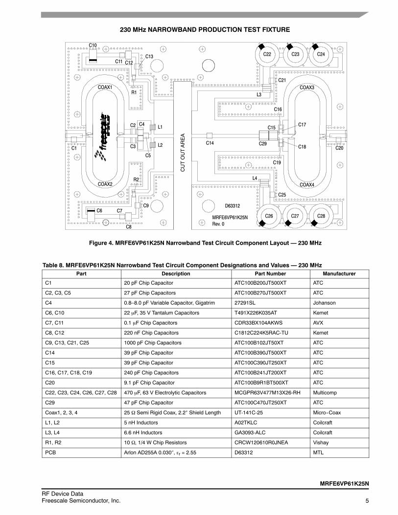
Figure 4. MRFE6VP61K25N Narrowband Test Circuit Component Layout — 230 MHz
C22 C23 C24
C21COAX3
L3
COAX4
C20
L4
C26 C27 C28
C25
MRFE6VP61K25NRev. 0
D63312
C8
C7C6
COAX2
COAX1
C9
R2
L2
L1
C5
R1
C13C11 C12
C10
C1
CUTOUTAREA
C14 C29
C15
C19
C16
C17
C18
C2
C3
C4
Table 8. MRFE6VP61K25N Narrowband Test Circuit Component Designations and Values — 230 MHzPart Description Part Number Manufacturer
C1 20 pF Chip Capacitor ATC100B200JT500XT ATC
C2, C3, C5 27 pF Chip Capacitors ATC100B270JT500XT ATC
C4 0.8–8.0 pF Variable Capacitor, Gigatrim 27291SL Johanson
C6, C10 22 F, 35 V Tantalum Capacitors T491X226K035AT Kemet
C7, C11 0.1 F Chip Capacitors CDR33BX104AKWS AVX
C8, C12 220 nF Chip Capacitors C1812C224K5RAC-TU Kemet
C9, C13, C21, C25 1000 pF Chip Capacitors ATC100B102JT50XT ATC
C14 39 pF Chip Capacitor ATC100B390JT500XT ATC
C15 39 pF Chip Capacitor ATC100C390JT250XT ATC
C16, C17, C18, C19 240 pF Chip Capacitors ATC100B241JT200XT ATC
C20 9.1 pF Chip Capacitor ATC100B9R1BT500XT ATC
C22, C23, C24, C26, C27, C28 470 F, 63 V Electrolytic Capacitors MCGPR63V477M13X26-RH Multicomp
C29 47 pF Chip Capacitor ATC100C470JT250XT ATC
Coax1, 2, 3, 4 25 Semi Rigid Coax, 2.2 Shield Length UT-141C-25 Micro--Coax
L1, L2 5 nH Inductors A02TKLC Coilcraft
L3, L4 6.6 nH Inductors GA3093-ALC Coilcraft
R1, R2 10 , 1/4 W Chip Resistors CRCW120610R0JNEA Vishay
PCB Arlon AD255A 0.030, r = 2.55 D63312 MTL
6RF Device Data
Freescale Semiconductor, Inc.
MRFE6VP61K25N
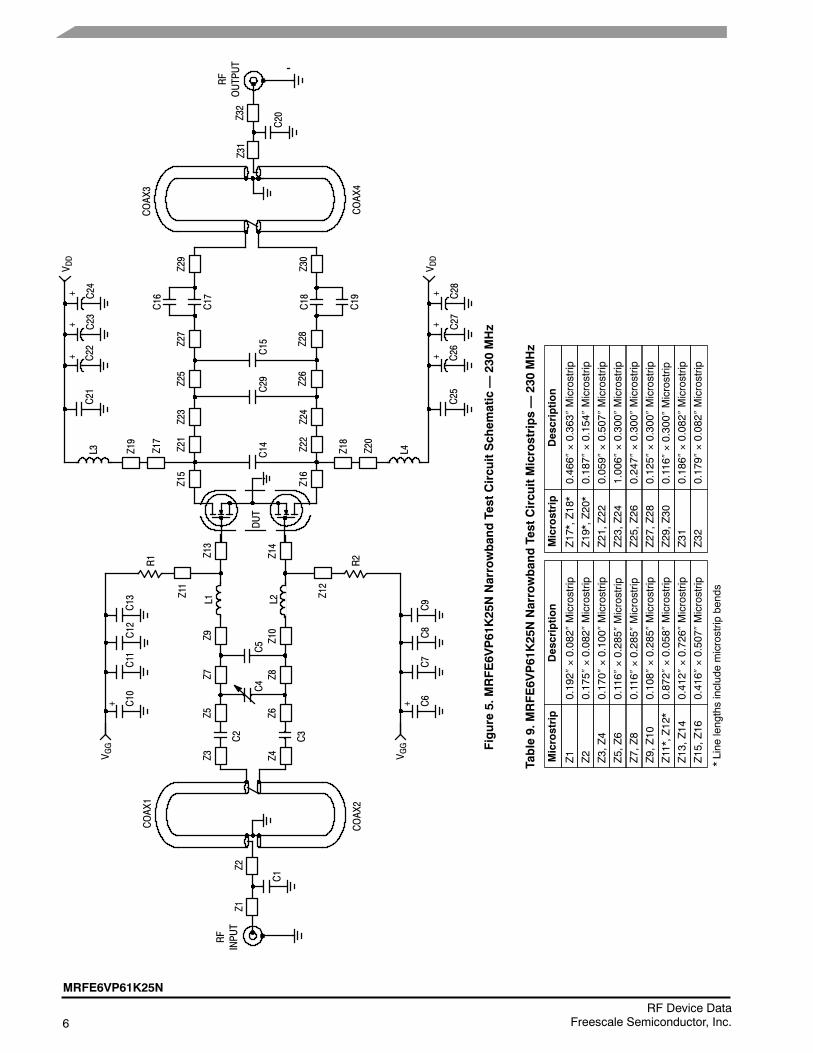
Z17*,Z18*
0.466
0.363
Microstrip
Z19*,Z20*
0.187
0.154
Microstrip
Z21,Z22
0.059
0.507
Microstrip
Z23,Z24
1.006
0.300
Microstrip
Z25,Z26
0.247
0.300
Microstrip
Z27,Z28
0.125
0.300
Microstrip
Z29,Z30
0.116
0.300
Microstrip
Z31
0.186
0.082
Microstrip
Z32
0.179
0.082
Microstrip
Description
Microstrip
Description
Microstrip
Z1
0.192
0.082
Microstrip
Z2
0.175
0.082
Microstrip
Z3,Z4
0.170
0.100
Microstrip
Z5,Z6
0.116
0.285
Microstrip
Z7,Z8
0.116
0.285
Microstrip
Z9,Z10
0.108
0.285
Microstrip
Z11*,Z12*
0.872
0.058
Microstrip
Z13,Z14
0.412
0.726
Microstrip
Z15,Z16
0.416
0.507
Microstrip
Figure
5.MRFE6V
P61K25NNarrowbandTestCircuitSchem
atic—
230MHz
Table9.MRFE6V
P61K25NNarrowbandTestCircuitMicrostrips—
230MHz
*Line
lengthsincludemicrostrip
bends
RF
INPUT
Z1
DUT
Z19
Z21
COAX1
COAX2
Z25
C10
Z15
Z16
V GG
V DD
C23+
Z3 Z4
C2
C3
Z5 Z6
Z7 Z8
RF
OUTPUT
COAX3
COAX4
Z32
Z9 Z10
L1
Z31
C11
L3C21
C22
Z22
Z26
C20
C12
C13
Z11
C24+
Z17
Z23
Z24
C29
Z27
Z28
R1
C1Z2
+
L2
Z13
Z14
Z12
R2
C6
V GG
C7
C8
C9
+
+
Z18
Z20
L4
V DD
C27+
C25
C26
C28+
+C15
C14
C17
C16
Z29
C19
C18
Z30
C4
C5
MRFE6VP61K25N
7RF Device DataFreescale Semiconductor, Inc.
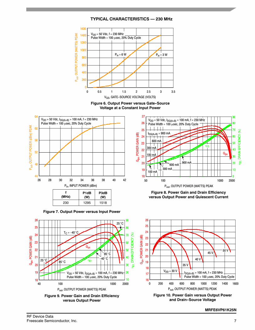
TYPICAL CHARACTERISTICS — 230 MHz
0
VGS, GATE--SOURCE VOLTAGE (VOLTS)
Figure 6. Output Power versus Gate--SourceVoltage at a Constant Input Power
0
P out,OUTPUTPOWER
(WATTS)PEAK
1200
1000
800
600
400
1.5 2 2.5 3
1600
1400
Pin = 6 W Pin = 3 W
0.5 1 3.5
VDD = 50 Vdc, f = 230 MHzPulse Width = 100 sec, 20% Duty Cycle
200
Pin, INPUT POWER (dBm)
40
56
52
44
P out,OUTPUTPOWER
(dBm
)PEAK
48
38363428 3230
60
64
26
VDD = 50 Vdc, IDQ(A+B) = 100 mA, f = 230 MHzPulse Width = 100 sec, 20% Duty Cycle
230 1295 1518
f(MHz)
P1dB(W)
P3dB(W)
Figure 7. Output Power versus Input Power
42
24
22
20
Pout, OUTPUT POWER (WATTS) PEAK
Figure 8. Power Gain and Drain Efficiencyversus Output Power and Quiescent Current
Gps,POWER
GAIN(dB)
D,DRAINEFFICIENCY(%)
23
21
IDQ(A+B) = 900 mA25
600 mA
100 mA
50 100 10000
80
70
60
50
40
30
20
26
90
300 mA
300 mA600 mA
900 mA
27
D
Gps
100 mA
VDD = 50 Vdc, IDQ(A+B) = 100 mA, f = 230 MHzPulse Width = 100 sec, 20% Duty Cycle
2000
19
18
10
D25_C
TC = –40_C
85_C
85_C
25_C
–40_C
Gps
VDD = 50 Vdc, IDQ(A+B) = 100 mA, f = 230 MHzPulse Width = 100 sec, 20% Duty Cycle
24
22
20
23
21
19
25
40 100 100010
80
70
60
50
40
30
20
26 90
Pout, OUTPUT POWER (WATTS) PEAK
Figure 9. Power Gain and Drain Efficiencyversus Output Power
Gps,POWER
GAIN(dB)
D,DRAINEFFICIENCY(%)
182000 0
Pout, OUTPUT POWER (WATTS) PEAK
Figure 10. Power Gain versus Output Powerand Drain--Source Voltage
25
24
Gps,POWER
GAIN(dB)
21
20
19
18
17
600 800 1000 1200 1400
23
22
VDD = 30 V
200 40016
35 V
45 V50 V
26
1600
IDQ(A+B) = 100 mA, f = 230 MHzPulse Width = 100 sec, 20% Duty Cycle
40 V
8RF Device Data
Freescale Semiconductor, Inc.
MRFE6VP61K25N
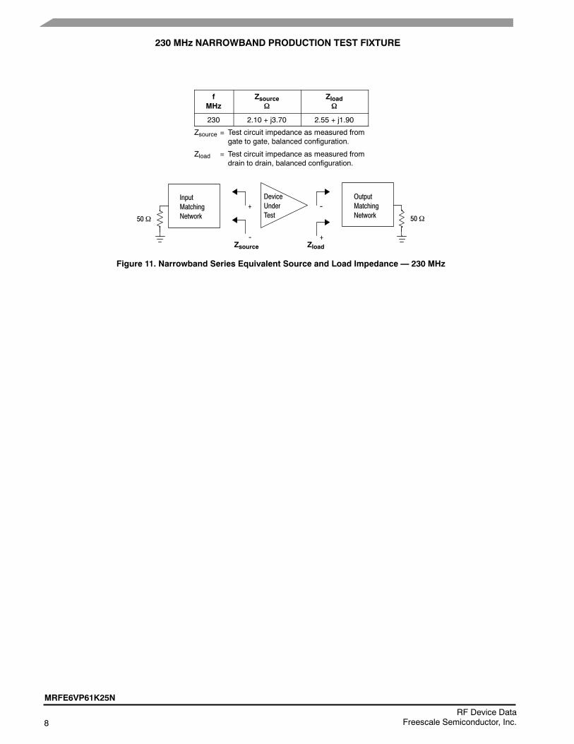
230 MHz NARROWBAND PRODUCTION TEST FIXTURE
fMHz
Zsource
Zload
230 2.10 + j3.70 2.55 + j1.90
Zsource = Test circuit impedance as measured fromgate to gate, balanced configuration.
Zload = Test circuit impedance as measured fromdrain to drain, balanced configuration.
Figure 11. Narrowband Series Equivalent Source and Load Impedance — 230 MHz
InputMatchingNetwork
DeviceUnderTest
OutputMatchingNetwork
--
-- +
+
Zsource Zload
5050
MRFE6VP61K25N
9RF Device DataFreescale Semiconductor, Inc.
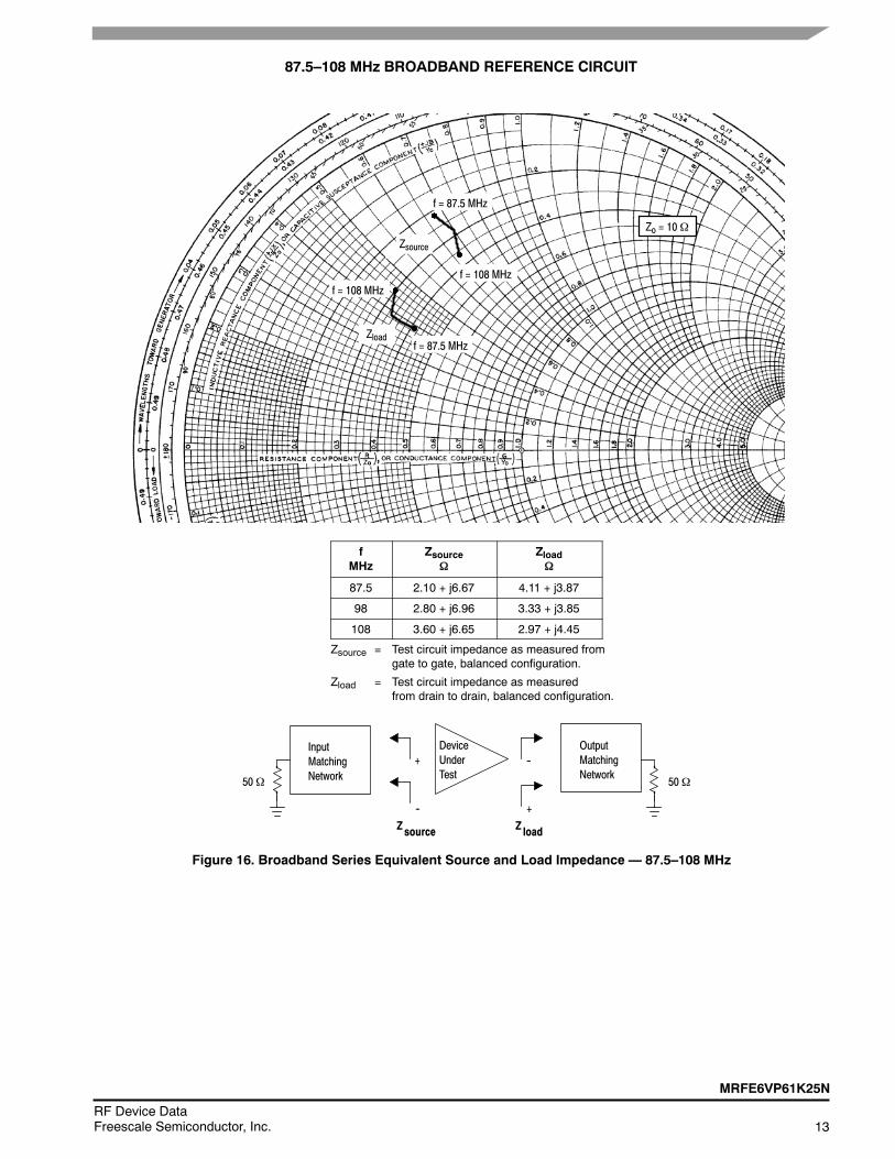
87.5–108 MHz BROADBAND REFERENCE CIRCUIT
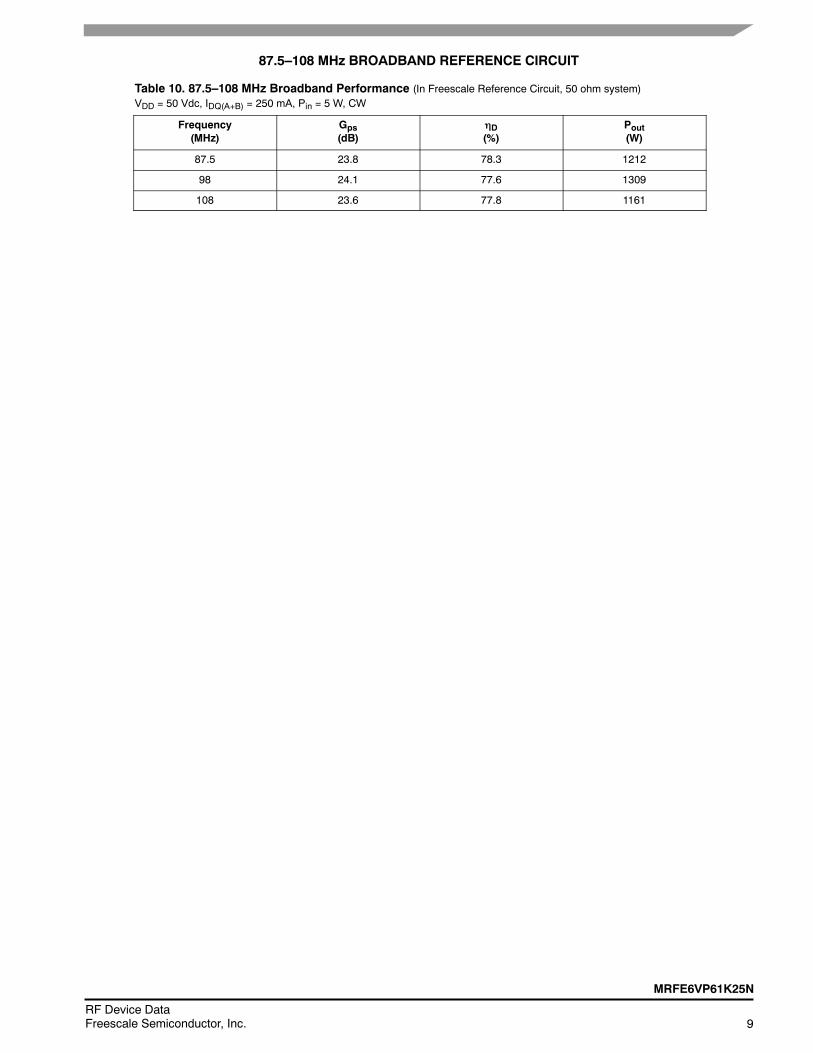
Table 10. 87.5–108 MHz Broadband Performance (In Freescale Reference Circuit, 50 ohm system)VDD = 50 Vdc, IDQ(A+B) = 250 mA, Pin = 5 W, CW
Frequency(MHz)
Gps(dB)
D(%)
Pout(W)
87.5 23.8 78.3 1212
98 24.1 77.6 1309
108 23.6 77.8 1161
10RF Device Data
Freescale Semiconductor, Inc.
MRFE6VP61K25N
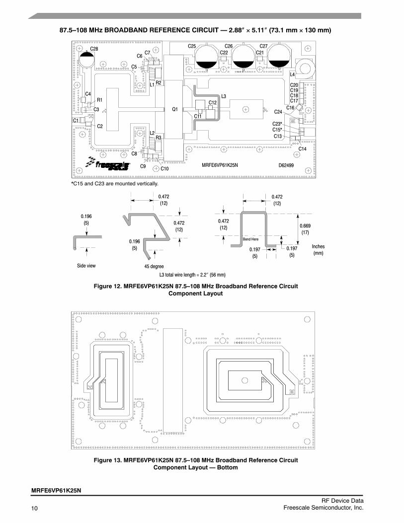
87.5–108 MHz BROADBAND REFERENCE CIRCUIT — 2.88 5.11 (73.1 mm 130 mm)
Figure 12. MRFE6VP61K25N 87.5–108 MHz Broadband Reference CircuitComponent Layout
MRFE6VP61K25N D62499
C28 C25 C26 C27C21C22
C17C18C19C20
C16
C23*
C24
C15*C13
C14
L4
L3C12
C11
C9
C8
C10
R3L2
L1 R2
C6
C5
C7
C1
C3
C4R1
C2
Inches(mm)
0.196(5)
Side view
0.196(5)
45 degree
0.472(12)
0.472(12)
0.472(12)
Bend Here
0.197(5)
0.197(5)
0.669(17)
0.472(12)
L3 total wire length = 2.2 (56 mm)
Q1
Figure 13. MRFE6VP61K25N 87.5–108 MHz Broadband Reference CircuitComponent Layout — Bottom
*C15 and C23 are mounted vertically.
MRFE6VP61K25N
11RF Device DataFreescale Semiconductor, Inc.
87.5–108 MHz BROADBAND REFERENCE CIRCUIT
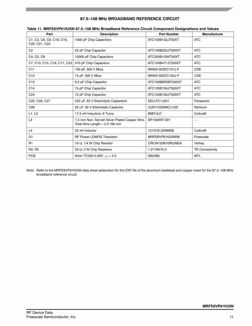
Table 11. MRFE6VP61K25N 87.5–108 MHz Broadband Reference Circuit Component Designations and ValuesPart Description Part Number Manufacturer
C1, C3, C6, C9, C18, C19,C20, C21, C22
1000 pF Chip Capacitors ATC100B102JT50XT ATC
C2 22 pF Chip Capacitor ATC100B220JT500XT ATC
C4, C5, C8 10000 pF Chip Capacitors ATC200B103KT50XT ATC
C7, C10, C15, C16, C17, C23 470 pF Chip Capacitors ATC100B471JT200XT ATC
C11 100 pF, 300 V Mica MIN02-002EC101J-F CDE
C12 15 pF, 300 V Mica MIN02-002CC150J-F CDE
C13 6.2 pF Chip Capacitor ATC100B6R2BT500XT ATC
C14 15 pF Chip Capacitor ATC100B150JT500XT ATC
C24 12 pF Chip Capacitor ATC100B120JT500XT ATC
C25, C26, C27 220 F, 63 V Electrolytic Capacitors EEU-FC1J221 Panasonic
C28 22 F, 35 V Electrolytic Capacitor UUD1V220MCL1GS Nichicon
L1, L2 17.5 nH Inductors, 6 Turns B06TJLC Coilcraft
L3 1.5 mm Non--Tarnish Silver Plated Copper Wire,Total Wire Length = 2.2/56 mm
SP1500NT-001 —
L4 22 nH Inductor 1212VS-22NMEB Coilcraft
Q1 RF Power LDMOS Transistor MRFE6VP61K25NR6 Freescale
R1 10 , 1/4 W Chip Resistor CRCW120610R0JNEA Vishay
R2, R3 33 , 2 W Chip Resistors 1-2176070-3 TE Connectivity
PCB Arlon TC350 0.030, r = 3.5 D62499 MTL
Note: Refer to the MRFE6VP61K25N data sheet addendum for the DXF file of the aluminum bedstead and copper insert for the 87.5–108 MHzbroadband reference circuit.
12RF Device Data
Freescale Semiconductor, Inc.
MRFE6VP61K25N
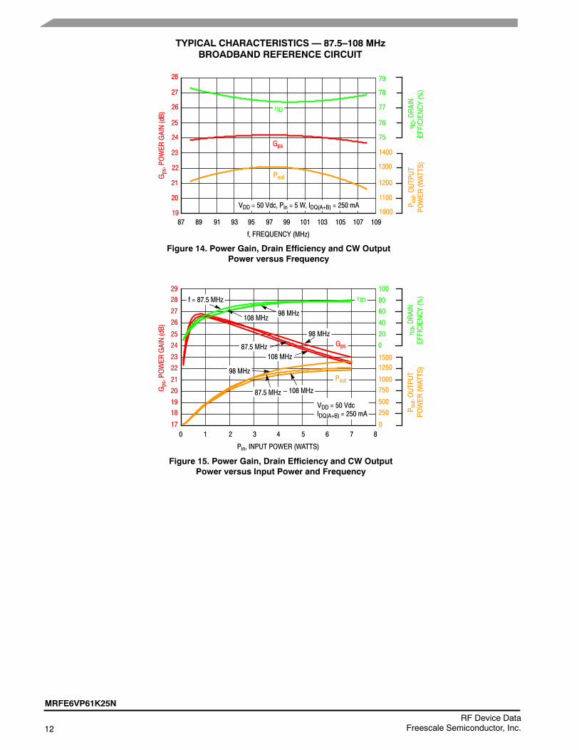
TYPICAL CHARACTERISTICS — 87.5–108 MHzBROADBAND REFERENCE CIRCUIT
93
Gps
f, FREQUENCY (MHz)
Figure 14. Power Gain, Drain Efficiency and CW OutputPower versus Frequency
28
27
26
1000
79
78
77
75
1400
1300
D,DRAIN
EFFICIENCY(%)
D
Gps,POWER
GAIN(dB)
25
24
23
22
21
1995 97 99 101 103 105 107
76
1200
P out,OUTPUT
POWER
(WATTS)
VDD = 50 Vdc, Pin = 5 W, IDQ(A+B) = 250 mA
Pout
9189 10987
17
29
00
100
1
26
23
60
40
20
0
1500
Pin, INPUT POWER (WATTS)
Figure 15. Power Gain, Drain Efficiency and CW OutputPower versus Input Power and Frequency
Gps,POWER
GAIN(dB)
24
21
18
2 3
28 80
Gps
D
108 MHz
f = 87.5 MHz
VDD = 50 VdclDQ(A+B) = 250 mA
98 MHz
4 8
108 MHz
20 1100
27
25
22
20
19
5 6 7
1250
1000750
500250
D,DRAIN
EFFICIENCY(%)
P out,OUTPUT
POWER
(WATTS)
Pout
98 MHz
108 MHz
87.5 MHz
98 MHz
87.5 MHz
MRFE6VP61K25N
13RF Device DataFreescale Semiconductor, Inc.
87.5–108 MHz BROADBAND REFERENCE CIRCUIT
Zo = 10
Zsource
f = 87.5 MHz
f = 108 MHz
Zload
f = 108 MHz
f = 87.5 MHz
fMHz
Zsource
Zload
87.5 2.10 + j6.67 4.11 + j3.87
98 2.80 + j6.96 3.33 + j3.85
108 3.60 + j6.65 2.97 + j4.45
Zsource = Test circuit impedance as measured fromgate to gate, balanced configuration.
Zload = Test circuit impedance as measuredfrom drain to drain, balanced configuration.
Figure 16. Broadband Series Equivalent Source and Load Impedance — 87.5–108 MHz
Zsource Z load
InputMatchingNetwork
DeviceUnderTest
OutputMatchingNetwork
--
-- +
+
5050

14RF Device Data
Freescale Semiconductor, Inc.
MRFE6VP61K25N
HARMONIC MEASUREMENTS — 87.5–108 MHzBROADBAND REFERENCE CIRCUIT
H2(175 MHz)
H3(262.5 MHz)
H4(350 MHz)
–37 dB –30 dB –42 dB
Center: 228.5 MHz Span: 350 MHz35 MHz
Figure 17. 87.5 MHz Harmonics @ 1215 W CW
H4
H3
H2
Fundamental (F1) 175 MHz –37 dB262.5 MHz –30 dB350 MHz –42 dB
H2H3H4
F1 87.5 MHz
MRFE6VP61K25N
15RF Device DataFreescale Semiconductor, Inc.
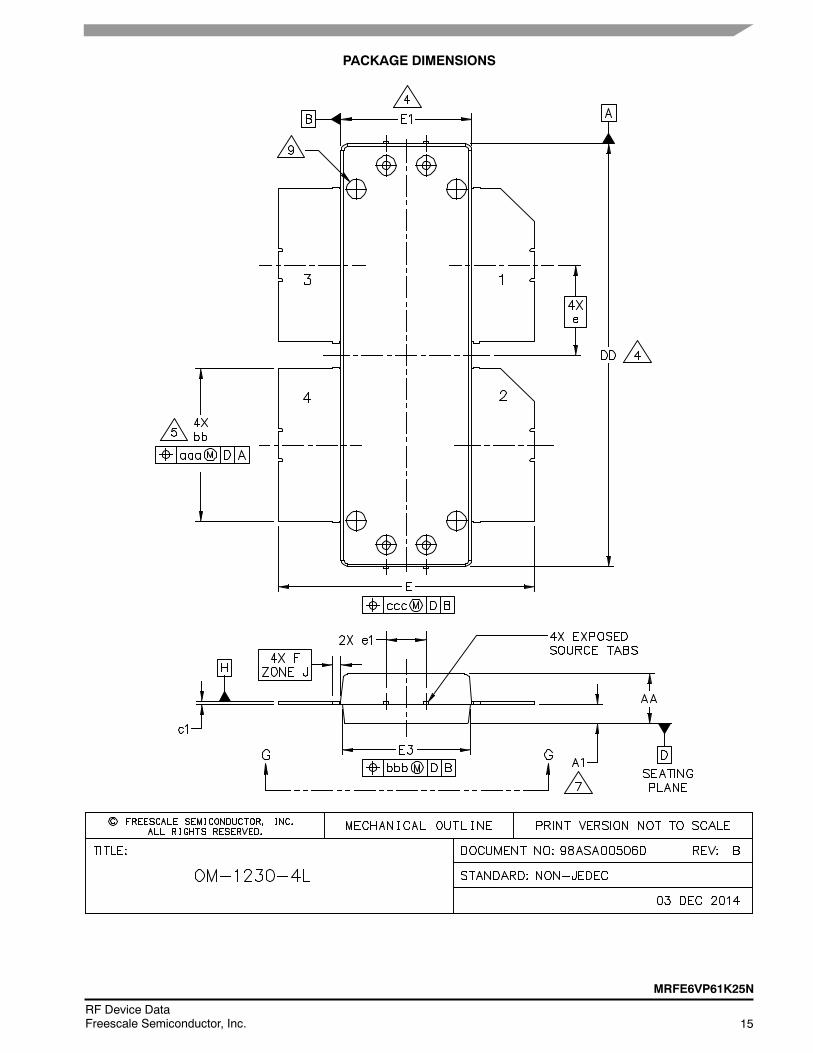
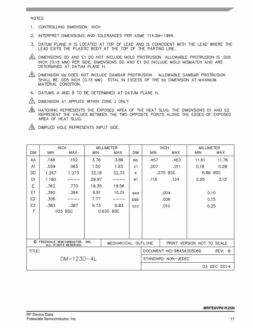
PACKAGE DIMENSIONS

16RF Device Data
Freescale Semiconductor, Inc.
MRFE6VP61K25N
MRFE6VP61K25N
17RF Device DataFreescale Semiconductor, Inc.
18RF Device Data
Freescale Semiconductor, Inc.
MRFE6VP61K25N
PRODUCT DOCUMENTATION, SOFTWARE AND TOOLS
Refer to the following resources to aid your design process.
Application Notes
AN1907: Solder Reflow Attach Method for High Power RF Devices in Over--Molded Plastic Packages AN1955: Thermal Measurement Methodology of RF Power AmplifiersEngineering Bulletins EB212: Using Data Sheet Impedances for RF LDMOS DevicesWhite Paper RFPLASTICWP: Designing with Plastic RF Power TransistorsSoftware Electromigration MTTF Calculator RF High Power Model .s2p FileDevelopment Tools
Printed Circuit Boards
For Software and Tools, do a Part Number search at http://www.freescale.com, and select the “Part Number” link. Go toSoftware & Tools on the part’s Product Summary page to download the respective tool.
REVISION HISTORY
The following table summarizes revisions to this document.
Revision Date Description
0 Feb. 2015 Initial Release of Data Sheet
1 Feb. 2015 Table 2, Maximum Ratings: added Total Device Dissipation, p. 2
Table 3, Thermal Characteristics: added CW Thermal Resistance, p. 2
Added Fig. 11, Narrowband Series Equivalent Source and Load Impedance -- 230 MHz, p. 8
MRFE6VP61K25N
19RF Device DataFreescale Semiconductor, Inc.
Information in this document is provided solely to enable system and softwareimplementers to use Freescale products. There are no express or implied copyrightlicenses granted hereunder to design or fabricate any integrated circuits based on theinformation in this document.
Freescale reserves the right to make changes without further notice to any productsherein. Freescale makes no warranty, representation, or guarantee regarding thesuitability of its products for any particular purpose, nor does Freescale assume anyliability arising out of the application or use of any product or circuit, and specificallydisclaims any and all liability, including without limitation consequential or incidentaldamages. “Typical” parameters that may be provided in Freescale data sheets and/orspecifications can and do vary in different applications, and actual performance mayvary over time. All operating parameters, including “typicals,” must be validated foreach customer application by customer’s technical experts. Freescale does not conveyany license under its patent rights nor the rights of others. Freescale sells productspursuant to standard terms and conditions of sale, which can be found at the followingaddress: freescale.com/SalesTermsandConditions.
Freescale and the Freescale logo are trademarks of Freescale Semiconductor, Inc.,Reg. U.S. Pat. & Tm. Off. All other product or service names are the property of theirrespective owners.E 2015 Freescale Semiconductor, Inc.
How to Reach Us:
Home Page:freescale.com
Web Support:freescale.com/support
Document Number: MRFE6VP61K25NRev. 1, 2/2015