Document Number: MW7IC2040N Technical Data RF LDMOS ...MW7IC2040NR1 MW7IC2040GNR1 MW7IC2040NBR1 1 RF...
29
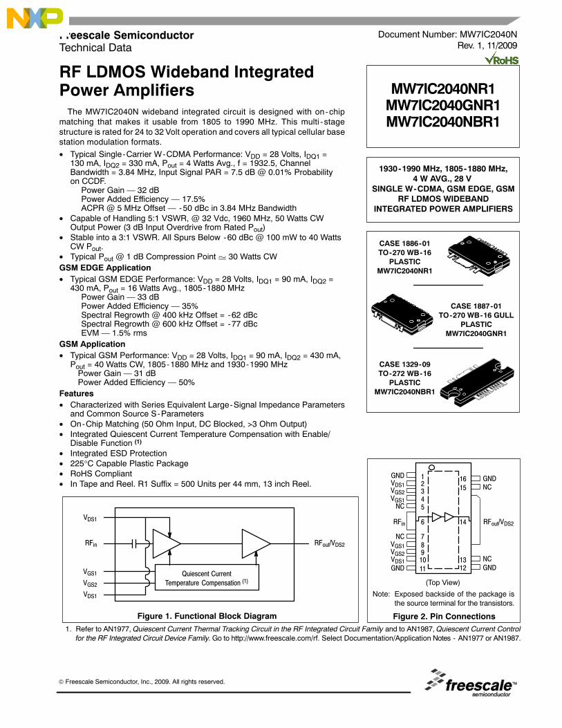
RF LDMOS Wideband Integrated Power Amplifiers The MW7IC2040N wideband integrated circuit is designed with on-chip matching that makes it usable from 1805 to 1990 MHz. This multi-stage structure is rated for 24 to 32 Volt operation and covers all typical cellular base station modulation formats. • Typical Single - Carrier W - CDMA Performance: V DD = 28 Volts, I DQ1 = 130 mA, I DQ2 = 330 mA, P out = 4 Watts Avg., f = 1932.5, Channel Bandwidth = 3.84 MHz, Input Signal PAR = 7.5 dB @ 0.01% Probability on CCDF. Power Gain 32 dB Power Added Efficiency 17.5% ACPR @ 5 MHz Offset - 50 dBc in 3.84 MHz Bandwidth • Capable of Handling 5:1 VSWR, @ 32 Vdc, 1960 MHz, 50 Watts CW Output Power (3 dB Input Overdrive from Rated P out ) • Stable into a 3:1 VSWR. All Spurs Below -60 dBc @ 100 mW to 40 Watts CW P out . • Typical P out @ 1 dB Compression Point ' 30 Watts CW GSM EDGE Application • Typical GSM EDGE Performance: V DD = 28 Volts, I DQ1 = 90 mA, I DQ2 = 430 mA, P out = 16 Watts Avg., 1805-1880 MHz Power Gain 33 dB Power Added Efficiency 35% Spectral Regrowth @ 400 kHz Offset = - 62 dBc Spectral Regrowth @ 600 kHz Offset = - 77 dBc EVM 1.5% rms GSM Application • Typical GSM Performance: V DD = 28 Volts, I DQ1 = 90 mA, I DQ2 = 430 mA, P out = 40 Watts CW, 1805-1880 MHz and 1930-1990 MHz Power Gain 31 dB Power Added Efficiency 50% Features • Characterized with Series Equivalent Large - Signal Impedance Parameters and Common Source S - Parameters • On - Chip Matching (50 Ohm Input, DC Blocked, >3 Ohm Output) • Integrated Quiescent Current Temperature Compensation with Enable/ Disable Function (1) • Integrated ESD Protection • 225°C Capable Plastic Package • RoHS Compliant • In Tape and Reel. R1 Suffix = 500 Units per 44 mm, 13 inch Reel. 1. Refer to AN1977, Quiescent Current Thermal Tracking Circuit in the RF Integrated Circuit Family and to AN1987, Quiescent Current Control for the RF Integrated Circuit Device Family . Go to http://www.freescale.com/rf. Select Documentation/Application Notes - AN1977 or AN1987. Document Number: MW7IC2040N Rev. 1, 11/2009 Freescale Semiconductor Technical Data MW7IC2040NR1 MW7IC2040GNR1 MW7IC2040NBR1 1930 - 1990 MHz, 1805 - 1880 MHz, 4 W AVG., 28 V SINGLE W - CDMA, GSM EDGE, GSM RF LDMOS WIDEBAND INTEGRATED POWER AMPLIFIERS CASE 1886 - 01 TO-270 WB-16 PLASTIC MW7IC2040NR1 CASE 1887 - 01 TO - 270 WB - 16 GULL PLASTIC MW7IC2040GNR1 CASE 1329 - 09 TO-272 WB-16 PLASTIC MW7IC2040NBR1 Figure 1. Functional Block Diagram Quiescent Current Temperature Compensation (1) V DS1 RF in V GS1 RF out /V DS2 V GS2 V DS1 (Top View) GND NC RF in V GS1 GND V DS1 RF out /V DS2 GND V GS2 V DS1 GND 2 3 4 5 6 7 8 16 15 14 13 12 9 10 11 1 V GS2 V GS1 NC NC NC Figure 2. Pin Connections Note: Exposed backside of the package is the source terminal for the transistors. © Freescale Semiconductor, Inc., 2009. All rights reserved.
Transcript of Document Number: MW7IC2040N Technical Data RF LDMOS ...MW7IC2040NR1 MW7IC2040GNR1 MW7IC2040NBR1 1 RF...
MW7IC2040NR1 MW7IC2040GNR1 MW7IC2040NBR1
1RF Device DataFreescale Semiconductor
RF LDMOS Wideband Integrated Power Amplifiers
The MW7IC2040N wideband integrated circuit is designed with on-chipmatching that makes it usable from 1805 to 1990 MHz. This multi -stagestructure is rated for 24 to 32 Volt operation and covers all typical cellular basestation modulation formats.
• Typical Single-Carrier W-CDMA Performance: VDD = 28 Volts, IDQ1 =130 mA, IDQ2 = 330 mA, Pout = 4 Watts Avg., f = 1932.5, ChannelBandwidth = 3.84 MHz, Input Signal PAR = 7.5 dB @ 0.01% Probabilityon CCDF.
Power Gain � 32 dBPower Added Efficiency � 17.5%ACPR @ 5 MHz Offset � -50 dBc in 3.84 MHz Bandwidth
• Capable of Handling 5:1 VSWR, @ 32 Vdc, 1960 MHz, 50 Watts CW Output Power (3 dB Input Overdrive from Rated Pout)
• Stable into a 3:1 VSWR. All Spurs Below -60 dBc @ 100 mW to 40 WattsCW Pout.
• Typical Pout @ 1 dB Compression Point � 30 Watts CWGSM EDGE Application• Typical GSM EDGE Performance: VDD = 28 Volts, IDQ1 = 90 mA, IDQ2 =
430 mA, Pout = 16 Watts Avg., 1805-1880 MHzPower Gain � 33 dBPower Added Efficiency � 35%Spectral Regrowth @ 400 kHz Offset = -62 dBcSpectral Regrowth @ 600 kHz Offset = -77 dBcEVM � 1.5% rms
GSM Application• Typical GSM Performance: VDD = 28 Volts, IDQ1 = 90 mA, IDQ2 = 430 mA,
Pout = 40 Watts CW, 1805-1880 MHz and 1930-1990 MHzPower Gain � 31 dBPower Added Efficiency � 50%
Features• Characterized with Series Equivalent Large-Signal Impedance Parameters
and Common Source S-Parameters• On-Chip Matching (50 Ohm Input, DC Blocked, >3 Ohm Output)• Integrated Quiescent Current Temperature Compensation with Enable/
Disable Function (1)
• Integrated ESD Protection• 225°C Capable Plastic Package• RoHS Compliant• In Tape and Reel. R1 Suffix = 500 Units per 44 mm, 13 inch Reel.
1. Refer to AN1977, Quiescent Current Thermal Tracking Circuit in the RF Integrated Circuit Family and to AN1987, Quiescent Current Controlfor the RF Integrated Circuit Device Family. Go to http://www.freescale.com/rf. Select Documentation/Application Notes - AN1977 or AN1987.
Document Number: MW7IC2040NRev. 1, 11/2009
Freescale SemiconductorTechnical Data
MW7IC2040NR1MW7IC2040GNR1MW7IC2040NBR1
1930-1990 MHz, 1805-1880 MHz,4 W AVG., 28 V
SINGLE W-CDMA, GSM EDGE, GSMRF LDMOS WIDEBAND
INTEGRATED POWER AMPLIFIERS
CASE 1886-01TO-270 WB-16
PLASTICMW7IC2040NR1
CASE 1887-01TO-270 WB-16 GULL
PLASTICMW7IC2040GNR1
CASE 1329-09TO-272 WB-16
PLASTICMW7IC2040NBR1
Figure 1. Functional Block Diagram
Quiescent Current
Temperature Compensation (1)
VDS1
RFin
VGS1
RFout/VDS2
VGS2
VDS1
(Top View)
GND
NC
RFin
VGS1
GNDVDS1
RFout/VDS2
GND
VGS2VDS1
GND
2345
6
78
16
15
14
1312
910
11
1
VGS2VGS1
NC
NC
NC
Figure 2. Pin Connections
Note: Exposed backside of the package isthe source terminal for the transistors.
© Freescale Semiconductor, Inc., 2009. All rights reserved.
2RF Device Data
Freescale Semiconductor
MW7IC2040NR1 MW7IC2040GNR1 MW7IC2040NBR1
Table 1. Maximum Ratings
Rating Symbol Value Unit
Drain-Source Voltage VDSS -0.5, +65 Vdc
Gate-Source Voltage VGS -0.5, +10 Vdc
Operating Voltage VDD 32, +0 Vdc
Storage Temperature Range Tstg -65 to +150 °C
Case Operating Temperature TC 150 °C
Operating Junction Temperature (1,2) TJ 225 °C
Input Power Pin 25 dBm
Table 2. Thermal Characteristics
Characteristic Symbol Value (2,3) Unit
Thermal Resistance, Junction to Case
W-CDMA(Pout = 4 W Avg., Case Temperature = 73°C) Stage 1, 28 Vdc, IDQ1 = 130 mA
Stage 2, 28 Vdc, IDQ2 = 330 mA
GSM EDGE(Pout = 16 W Avg., Case Temperature = 76°C) Stage 1, 28 Vdc, IDQ1 = 130 mA
Stage 2, 28 Vdc, IDQ2 = 330 mAGSM(Pout = 40 W Avg., Case Temperature = 79°C) Stage 1, 28 Vdc, IDQ1 = 130 mA
Stage 2, 28 Vdc, IDQ2 = 330 mA
RθJC
4.01.5
4.11.4
3.91.3
°C/W
Table 3. ESD Protection Characteristics
Test Methodology Class
Human Body Model (per JESD22-A114) 1B (Minimum)
Machine Model (per EIA/JESD22-A115) A (Minimum)
Charge Device Model (per JESD22-C101) III (Minimum)
Table 4. Moisture Sensitivity Level
Test Methodology Rating Package Peak Temperature Unit
Per JESD22-A113, IPC/JEDEC J-STD-020 3 260 °C
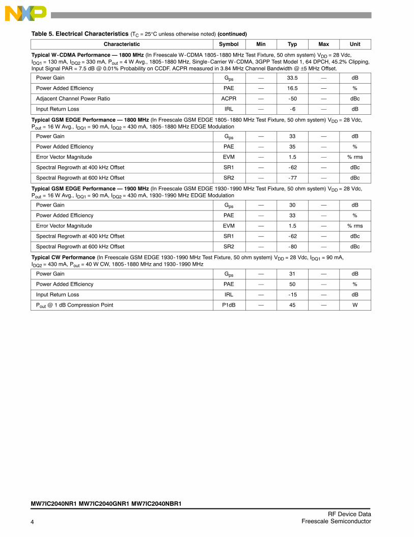
Table 5. Electrical Characteristics (TC = 25°C unless otherwise noted)
Characteristic Symbol Min Typ Max Unit
Stage 1 � Off Characteristics
Zero Gate Voltage Drain Leakage Current(VDS = 65 Vdc, VGS = 0 Vdc)
IDSS � � 10 μAdc
Zero Gate Voltage Drain Leakage Current(VDS = 28 Vdc, VGS = 0 Vdc)
IDSS � � 1 μAdc
Gate-Source Leakage Current(VGS = 1.5 Vdc, VDS = 0 Vdc)
IGSS � � 1 μAdc
Stage 1 � On Characteristics
Gate Threshold Voltage(VDS = 10 Vdc, ID = 25 μAdc)
VGS(th) 1.2 2 2.7 Vdc
Gate Quiescent Voltage(VDS = 28 Vdc, IDQ1 = 130 mAdc)
VGS(Q) � 2.7 � Vdc
Fixture Gate Quiescent Voltage(VDD = 28 Vdc, IDQ1 = 130 mAdc, Measured in Functional Test)
VGG(Q) 13 14.5 16 Vdc
1. Continuous use at maximum temperature will affect MTTF.2. MTTF calculator available at http://www.freescale.com/rf. Select Software & Tools/Development Tools/Calculators to access MTTF
calculators by product.3. Refer to AN1955, Thermal Measurement Methodology of RF Power Amplifiers. Go to http://www.freescale.com/rf.
Select Documentation/Application Notes - AN1955. (continued)
MW7IC2040NR1 MW7IC2040GNR1 MW7IC2040NBR1
3RF Device DataFreescale Semiconductor
Table 5. Electrical Characteristics (TC = 25°C unless otherwise noted) (continued)
Characteristic Symbol Min Typ Max Unit
Stage 2 � Off Characteristics
Zero Gate Voltage Drain Leakage Current(VDS = 65 Vdc, VGS = 0 Vdc)
IDSS � � 10 μAdc
Zero Gate Voltage Drain Leakage Current(VDS = 28 Vdc, VGS = 0 Vdc)
IDSS � � 1 μAdc
Gate-Source Leakage Current(VGS = 1.5 Vdc, VDS = 0 Vdc)
IGSS � � 1 μAdc
Stage 2 � On Characteristics
Gate Threshold Voltage(VDS = 10 Vdc, ID = 140 μAdc)
VGS(th) 1.2 2 2.7 Vdc
Gate Quiescent Voltage(VDS = 28 Vdc, IDQ2 = 330 mAdc)
VGS(Q) � 2.8 � Vdc
Fixture Gate Quiescent Voltage(VDD = 28 Vdc, IDQ2 = 330 mAdc, Measured in Functional Test)
VGG(Q) 7 8 9 Vdc
Drain-Source On-Voltage(VGS = 10 Vdc, ID = 1 Adc)
VDS(on) 0.2 0.39 1.2 Vdc
Stage 2 � Dynamic Characteristics (1)
Output Capacitance(VDS = 28 Vdc ± 30 mV(rms)ac @ 1 MHz, VGS = 0 Vdc)
Coss � 246 � pF
Functional Tests (3) (In Freescale Test Fixture, 50 ohm system) VDD = 28 Vdc, IDQ1 = 130 mA, IDQ2 = 330 mA, Pout = 4 W Avg.,f = 1932.5 MHz, Single-Carrier W-CDMA, 3GPP Test Model 1, 64 DPCH, 45.2% Clipping, Input Signal PAR = 7.5 dB @ 0.01% Probability onCCDF. ACPR measured in 3.84 MHz Channel Bandwidth @ ±5 MHz Offset.
Power Gain Gps 29.5 32 34.5 dB
Power Added Efficiency PAE 16 17.5 � %
Adjacent Channel Power Ratio ACPR � -50 -46 dBc
Input Return Loss IRL � -15 -8 dB
Typical Performances (In Freescale Test Fixture, 50 ohm system) VDD = 28 Vdc, IDQ1 = 130 mA, IDQ2 = 330 mA, 1930-1990 MHz
Pout @ 1 dB Compression Point, CW P1dB � 30 � W
IMD Symmetry @ 22 W PEP, Pout where IMD Third OrderIntermodulation � 30 dBc (Delta IMD Third Order Intermodulationbetween Upper and Lower Sidebands > 2 dB)
IMDsym� 60 �
MHz
VBW Resonance Point(IMD Third Order Intermodulation Inflection Point)
VBWres � 65 � MHz
Quiescent Current Accuracy over Temperature (2)
with 5.6 kΩ Gate Feed Resistors ( -30 to 85°C)ΔIQT � ±3 � %
Gain Flatness in 60 MHz Bandwidth @ Pout = 4 W Avg. GF � 1.2 � dB
Average Deviation from Linear Phase in 60 MHz Bandwidth@ Pout = 30 W CW
Φ � 0.5 � °
Average Group Delay @ Pout = 30 W CW, f = 1960 MHz Delay � 2.5 � ns
Part - to-Part Insertion Phase Variation @ Pout = 30 W CW,f = 1960 MHz, Six Sigma Window
ΔΦ � 33 � °
Gain Variation over Temperature(-30°C to +85°C)
ΔG � 0.029 � dB/°C
Output Power Variation over Temperature(-30°C to +85°C)
ΔP1dB � 0.003 � dBm/°C
1. Part internally matched both on input and output.2. Refer to AN1977, Quiescent Current Thermal Tracking Circuit in the RF Integrated Circuit Family and to AN1987, Quiescent Current Control
for the RF Integrated Circuit Device Family. Go to http://www.freescale.com/rf. Select Documentation/Application Notes - AN1977 orAN1987.
3. Measurement made with device in straight lead configuration before any lead forming operation is applied.(continued)
4RF Device Data
Freescale Semiconductor
MW7IC2040NR1 MW7IC2040GNR1 MW7IC2040NBR1
Table 5. Electrical Characteristics (TC = 25°C unless otherwise noted) (continued)
Characteristic Symbol Min Typ Max Unit
Typical W-CDMA Performance � 1800 MHz (In Freescale W-CDMA 1805-1880 MHz Test Fixture, 50 ohm system) VDD = 28 Vdc,IDQ1 = 130 mA, IDQ2 = 330 mA, Pout = 4 W Avg., 1805-1880 MHz, Single-Carrier W-CDMA, 3GPP Test Model 1, 64 DPCH, 45.2% Clipping,Input Signal PAR = 7.5 dB @ 0.01% Probability on CCDF. ACPR measured in 3.84 MHz Channel Bandwidth @ ±5 MHz Offset.
Power Gain Gps � 33.5 � dB
Power Added Efficiency PAE � 16.5 � %
Adjacent Channel Power Ratio ACPR � -50 � dBc
Input Return Loss IRL � -6 � dB
Typical GSM EDGE Performance � 1800 MHz (In Freescale GSM EDGE 1805-1880 MHz Test Fixture, 50 ohm system) VDD = 28 Vdc,Pout = 16 W Avg., IDQ1 = 90 mA, IDQ2 = 430 mA, 1805-1880 MHz EDGE Modulation
Power Gain Gps � 33 � dB
Power Added Efficiency PAE � 35 � %
Error Vector Magnitude EVM � 1.5 � % rms
Spectral Regrowth at 400 kHz Offset SR1 � -62 � dBc
Spectral Regrowth at 600 kHz Offset SR2 � -77 � dBc
Typical GSM EDGE Performance � 1900 MHz (In Freescale GSM EDGE 1930-1990 MHz Test Fixture, 50 ohm system) VDD = 28 Vdc,Pout = 16 W Avg., IDQ1 = 90 mA, IDQ2 = 430 mA, 1930-1990 MHz EDGE Modulation
Power Gain Gps � 30 � dB
Power Added Efficiency PAE � 33 � %
Error Vector Magnitude EVM � 1.5 � % rms
Spectral Regrowth at 400 kHz Offset SR1 � -62 � dBc
Spectral Regrowth at 600 kHz Offset SR2 � -80 � dBc
Typical CW Performance (In Freescale GSM EDGE 1930-1990 MHz Test Fixture, 50 ohm system) VDD = 28 Vdc, IDQ1 = 90 mA,IDQ2 = 430 mA, Pout = 40 W CW, 1805-1880 MHz and 1930-1990 MHz
Power Gain Gps � 31 � dB
Power Added Efficiency PAE � 50 � %
Input Return Loss IRL � -15 � dB
Pout @ 1 dB Compression Point P1dB � 45 � W
MW7IC2040NR1 MW7IC2040GNR1 MW7IC2040NBR1
5RF Device DataFreescale Semiconductor
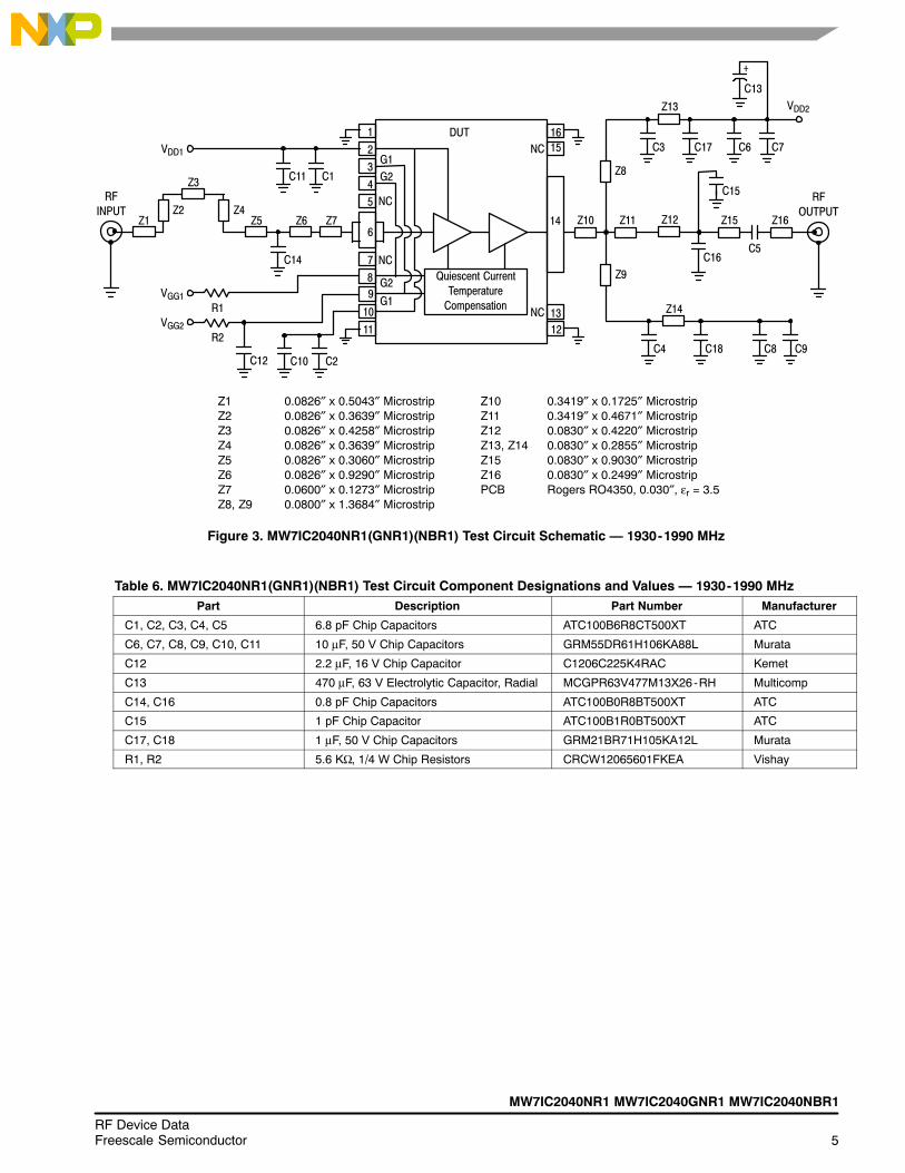
Z10 0.3419″ x 0.1725″ MicrostripZ11 0.3419″ x 0.4671″ MicrostripZ12 0.0830″ x 0.4220″ MicrostripZ13, Z14 0.0830″ x 0.2855″ MicrostripZ15 0.0830″ x 0.9030″ MicrostripZ16 0.0830″ x 0.2499″ MicrostripPCB Rogers RO4350, 0.030″, εr = 3.5
Z1 0.0826″ x 0.5043″ MicrostripZ2 0.0826″ x 0.3639″ MicrostripZ3 0.0826″ x 0.4258″ MicrostripZ4 0.0826″ x 0.3639″ MicrostripZ5 0.0826″ x 0.3060″ MicrostripZ6 0.0826″ x 0.9290″ MicrostripZ7 0.0600″ x 0.1273″ MicrostripZ8, Z9 0.0800″ x 1.3684″ Microstrip
Figure 3. MW7IC2040NR1(GNR1)(NBR1) Test Circuit Schematic � 1930-1990 MHz
R1
RF
INPUT
VGG1
Z10
RF
OUTPUT
C5
C3
VDD2
1
2
3
4
5
6
7
8
14
13
1211
10
9
15
16DUT
Z6
C1
VDD1
Z8
Quiescent Current
Temperature
Compensation
Z1
Z9
Z11 Z12
C11
VGG2
C12 C10 C2
Z15
C17 C6
C13
+
C4 C18 C8 C9
Z7
C14
R2
C16
C15
Z16
Z13
C7
Z14
Z2
Z3
Z4Z5
NC
NCG1
G2
NC
NC
G2
G1
Table 6. MW7IC2040NR1(GNR1)(NBR1) Test Circuit Component Designations and Values � 1930-1990 MHzPart Description Part Number Manufacturer
C1, C2, C3, C4, C5 6.8 pF Chip Capacitors ATC100B6R8CT500XT ATC
C6, C7, C8, C9, C10, C11 10 μF, 50 V Chip Capacitors GRM55DR61H106KA88L Murata
C12 2.2 μF, 16 V Chip Capacitor C1206C225K4RAC Kemet
C13 470 μF, 63 V Electrolytic Capacitor, Radial MCGPR63V477M13X26-RH Multicomp
C14, C16 0.8 pF Chip Capacitors ATC100B0R8BT500XT ATC
C15 1 pF Chip Capacitor ATC100B1R0BT500XT ATC
C17, C18 1 μF, 50 V Chip Capacitors GRM21BR71H105KA12L Murata
R1, R2 5.6 KΩ, 1/4 W Chip Resistors CRCW12065601FKEA Vishay
6RF Device Data
Freescale Semiconductor
MW7IC2040NR1 MW7IC2040GNR1 MW7IC2040NBR1
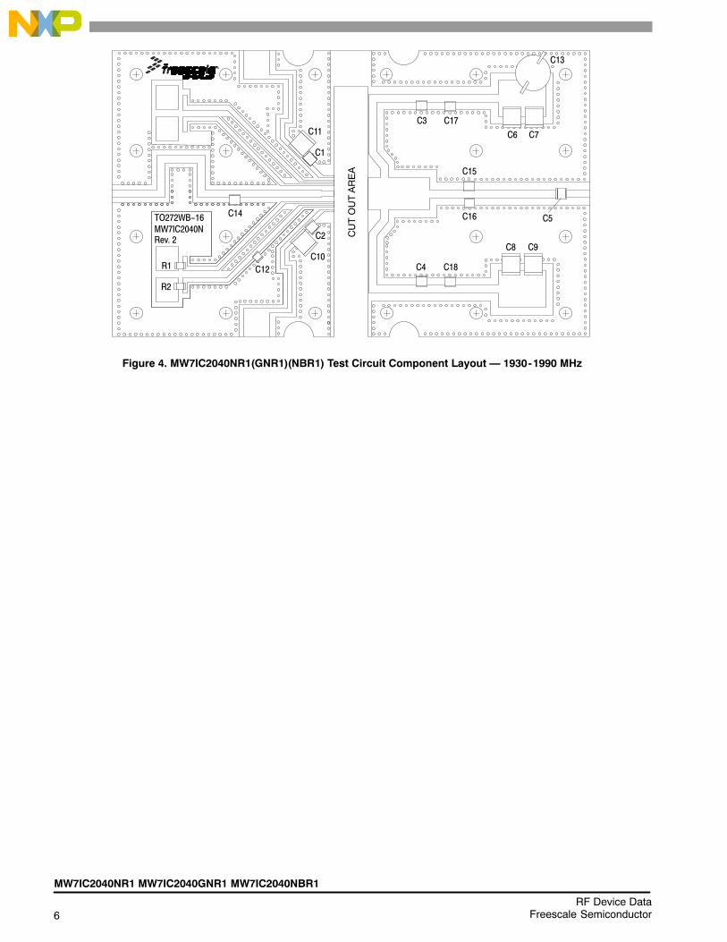
Figure 4. MW7IC2040NR1(GNR1)(NBR1) Test Circuit Component Layout � 1930-1990 MHzC
UT
OU
T A
RE
A
C14
R1
R2
C12
C10
C2
C1
C11
C4 C18
C8 C9
C16
C15
C5
C6 C7
C13
C3 C17
MW7IC2040NRev. 2
TO272WB−16
MW7IC2040NR1 MW7IC2040GNR1 MW7IC2040NBR1
7RF Device DataFreescale Semiconductor
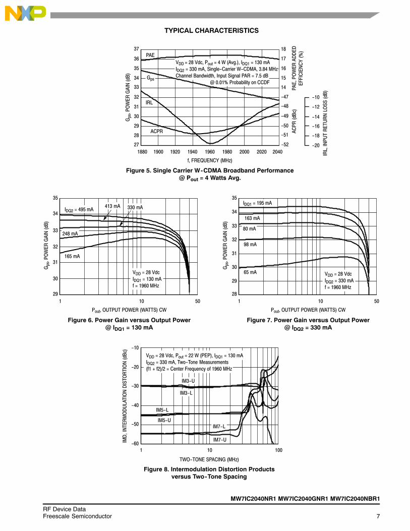
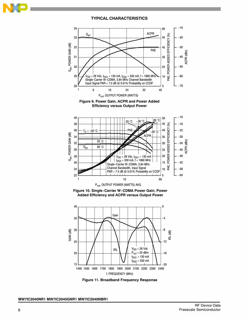
TYPICAL CHARACTERISTICS
IRL,
IN
PU
T R
ET
UR
N L
OS
S (
dB)
1880
IRL
Gps
ACPR
f, FREQUENCY (MHz)
Figure 5. Single Carrier W-CDMA Broadband Performance@ Pout = 4 Watts Avg.
−18
−10
−12
−14
−16
27
37
36
35
−52
18
17
16
15
−47
−48
−49
−50
PA
E, P
OW
ER
AD
DE
D
EF
FIC
IEN
CY
(%
)
Gps
, PO
WE
R G
AIN
(dB
)
34
33
32
31
30
29
1900 1920 1940 1960 1980 2000 2020 2040
14
−51
−20
AC
PR
(dB
c)
Figure 6. Power Gain versus Output Power@ IDQ1 = 130 mA
29
35
1
Pout, OUTPUT POWER (WATTS) CW
VDD = 28 Vdc
IDQ1 = 130 mA
f = 1960 MHz
33
32
31
10 50
Gps
, PO
WE
R G
AIN
(dB
)
34IDQ2 = 495 mA
248 mA
28
30
165 mA
330 mA413 mA
PAE
VDD = 28 Vdc, Pout = 4 W (Avg.), IDQ1 = 130 mA
IDQ2 = 330 mA, Single−Carrier W−CDMA, 3.84 MHz
Channel Bandwidth, Input Signal PAR = 7.5 dB
@ 0.01% Probability on CCDF
Figure 7. Power Gain versus Output Power@ IDQ2 = 330 mA
28
35
1
Pout, OUTPUT POWER (WATTS) CW
VDD = 28 Vdc
IDQ2 = 330 mA
f = 1960 MHz
33
32
31
10 50
Gps
, PO
WE
R G
AIN
(dB
)
34
IDQ1 = 195 mA
3065 mA
163 mA
29
98 mA
80 mA
Figure 8. Intermodulation Distortion Productsversus Two-Tone Spacing
TWO−TONE SPACING (MHz)
10
−60
−10
−20
−30
−50
1 100
IMD
, IN
TE
RM
OD
ULA
TIO
N D
IST
OR
TIO
N (
dBc)
−40
IM3−U
IM3−L
IM5−U
IM5−L
IM7−L
IM7−U
VDD = 28 Vdc, Pout = 22 W (PEP), IDQ1 = 130 mA
IDQ2 = 330 mA, Two−Tone Measurements
(f1 + f2)/2 = Center Frequency of 1960 MHz
8RF Device Data
Freescale Semiconductor
MW7IC2040NR1 MW7IC2040GNR1 MW7IC2040NBR1
TYPICAL CHARACTERISTICS
Figure 9. Power Gain, ACPR and Power AddedEfficiency versus Output Power
34
Pout, OUTPUT POWER (WATTS)
32
30
28
8
33
31
29
1 16 24 40
5
65
55
45
35
25
15
PA
E, P
OW
ER
AD
DE
D E
FF
ICIE
NC
Y (
%)
32
VDD = 28 Vdc, IDQ1 = 130 mA, IDQ2 = 330 mA, f = 1960 MHzSingle−Carrier W−CDMA, 3.84 MHz Channel BandwidthInput Signal PAR = 7.5 dB @ 0.01% Probability on CCDF
ACPR
AC
PR
(dB
c)
−70
−10
−20
−30
−50
−40
−60
Gps
, PO
WE
R G
AIN
(dB
)
Gps
Figure 10. Single-Carrier W-CDMA Power Gain, PowerAdded Efficiency and ACPR versus Output Power
PAE
40
Pout, OUTPUT POWER (WATTS) AVG.
36
32
28
38
34
30
1 10 60
5
50
45
40
35
25
15
PA
E, P
OW
ER
AD
DE
D E
FF
ICIE
NC
Y (
%)
VDD = 28 Vdc, IDQ1 = 130 mAIDQ2 = 330 mA, f = 1960 MHz
ACPR
AC
PR
(dB
c)
−64
−10
−34
−40
−52
−46
−58
Gps
, PO
WE
R G
AIN
(dB
)
Gps
22
24
26
10
20
30
TC = −30�C
85�C
25�C
−30�C25�C 85�C
−30�CPAE
Single−Carrier W−CDMA, 3.84 MHzChannel Bandwidth, Input SignalPAR = 7.5 dB @ 0.01% Probability on CCDF
Figure 11. Broadband Frequency Response
15
40
1400
f, FREQUENCY (MHz)
30
25
1500
GA
IN (
dB)
35Gain
1600 1700 1800 1900 2000 2300 2400
IRL
−20
0
−4
−8
−12
−16
IRL
(dB
)
20
VDD = 28 Vdc
Pout = 25 dBm
IDQ1 = 130 mA
IDQ2 = 330 mA
2100 2200
−28
−22
−16
MW7IC2040NR1 MW7IC2040GNR1 MW7IC2040NBR1
9RF Device DataFreescale Semiconductor
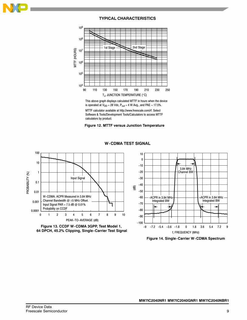
TYPICAL CHARACTERISTICS
250
109
90
TJ, JUNCTION TEMPERATURE (°C)
Figure 12. MTTF versus Junction Temperature
This above graph displays calculated MTTF in hours when the device
is operated at VDD = 28 Vdc, Pout = 4 W Avg., and PAE = 17.5%.
MTTF calculator available at http://www.freescale.com/rf. Select
Software & Tools/Development Tools/Calculators to access MTTF
calculators by product.
107
106
104
110 130 150 170 190
MT
TF
(H
OU
RS
)
210 230
105
108
1st Stage 2nd Stage
W-CDMA TEST SIGNAL
0.0001
100
0
PEAK−TO−AVERAGE (dB)
Figure 13. CCDF W-CDMA 3GPP, Test Model 1, 64 DPCH, 45.2% Clipping, Single-Carrier Test Signal
10
1
0.1
0.01
0.001
2 4 6 8
PR
OB
AB
ILIT
Y (
%)
W−CDMA. ACPR Measured in 3.84 MHz
Channel Bandwidth @ ±5 MHz Offset.
Input Signal PAR = 7.5 dB @ 0.01%
Probability on CCDF
Input Signal
101 3 5 7 9
−60
−100
10
(dB
)
−20
−30
−40
−50
−70
−80
−90
3.84 MHzChannel BW
7.21.8 5.43.60−1.8−3.6−5.4−9 9
f, FREQUENCY (MHz)
Figure 14. Single-Carrier W-CDMA Spectrum
−7.2
−ACPR in 3.84 MHzIntegrated BW
+ACPR in 3.84 MHzIntegrated BW
−10
0
10RF Device Data
Freescale Semiconductor
MW7IC2040NR1 MW7IC2040GNR1 MW7IC2040NBR1
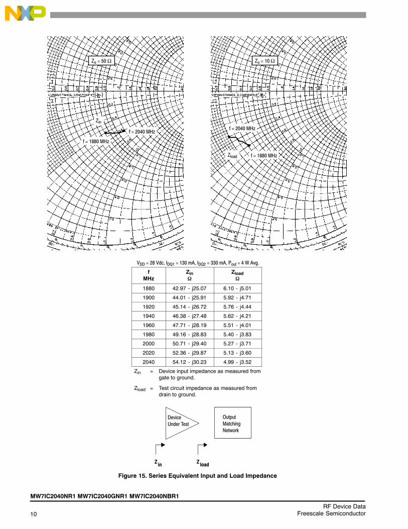
Zo = 50 Ω
f = 2040 MHz
f = 1880 MHz
Zin
Zo = 10 Ω
Zload
f = 2040 MHz
f = 1880 MHz
VDD = 28 Vdc, IDQ1 = 130 mA, IDQ2 = 330 mA, Pout = 4 W Avg.
fMHz
Zin�
Zload�
1880 42.97 - j25.07 6.10 - j5.01
1900 44.01 - j25.91 5.92 - j4.71
1920 45.14 - j26.72 5.76 - j4.44
1940 46.38 - j27.48 5.62 - j4.21
1960 47.71 - j28.19 5.51 - j4.01
1980 49.16 - j28.83 5.40 - j3.83
2000 50.71 - j29.40 5.27 - j3.71
2020 52.36 - j29.87 5.13 - j3.60
2040 54.12 - j30.23 4.99 - j3.52
Zin = Device input impedance as measured from gate to ground.
Zload = Test circuit impedance as measured fromdrain to ground.
Figure 15. Series Equivalent Input and Load Impedance
Zin
Zload
Device
Under Test
Output
Matching
Network
MW7IC2040NR1 MW7IC2040GNR1 MW7IC2040NBR1
11RF Device DataFreescale Semiconductor
ALTERNATIVE PEAK TUNE LOAD PULL CHARACTERISTICS
17
P3dB = 47.74 dBm (59 W)
Pin, INPUT POWER (dBm)
46
4318 21
Actual
Ideal
P1dB = 47.06 dBm (51 W)
47
45Pou
t, O
UT
PU
T P
OW
ER
(dB
m)
NOTE: Load Pull Test Fixture Tuned for Peak P1dB Output Power @ 28 V
48
49
50
53
161514131211
VDD = 28 Vdc, IDQ1 = 130 mA, IDQ2 = 330 mA
Pulsed CW, 10 μsec(on), 10% Duty Cycle, f = 1930 MHz44
51
52
19 20
Test Impedances per Compression Level
ZsourceΩ
ZloadΩ
P1dB 49.30 + j8.40 3.60 - j4.50
Figure 16. Pulsed CW Output Power versus Input Power @ 28 V @ 1930 MHz
17
P3dB = 47.88 dBm (61 W)
Pin, INPUT POWER (dBm)
46
18 23
Actual
Ideal
P1dB = 47.37 dBm (55 W)
47
45Pou
t, O
UT
PU
T P
OW
ER
(dB
m)
NOTE: Load Pull Test Fixture Tuned for Peak P1dB Output Power @ 28 V
48
49
50
53
1613
VDD = 28 Vdc, IDQ1 = 130 mA, IDQ2 = 330 mA
Pulsed CW, 10 μsec(on), 10% Duty Cycle, f = 1990 MHz
51
44
431514
52
19 20 21 22
Test Impedances per Compression Level
ZsourceΩ
ZloadΩ
P1dB 50.0 - j4.90 3.40 - j5.10
Figure 17. Pulsed CW Output Power versus Input Power @ 28 V @ 1990 MHz
12RF Device Data
Freescale Semiconductor
MW7IC2040NR1 MW7IC2040GNR1 MW7IC2040NBR1
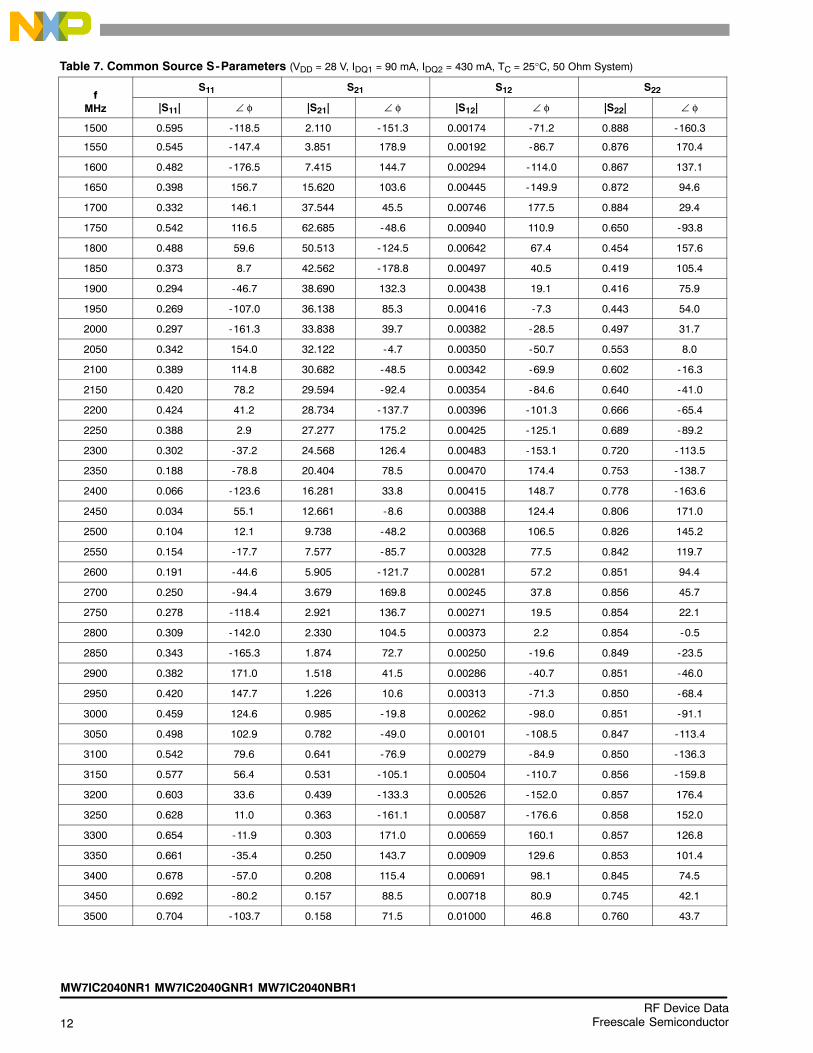
Table 7. Common Source S-Parameters (VDD = 28 V, IDQ1 = 90 mA, IDQ2 = 430 mA, TC = 25°C, 50 Ohm System)
fS11 S21 S12 S22f
MHz |S11| ∠ φ |S21| ∠ φ |S12| ∠ φ |S22| ∠ φ
1500 0.595 -118.5 2.110 -151.3 0.00174 -71.2 0.888 -160.3
1550 0.545 -147.4 3.851 178.9 0.00192 -86.7 0.876 170.4
1600 0.482 -176.5 7.415 144.7 0.00294 -114.0 0.867 137.1
1650 0.398 156.7 15.620 103.6 0.00445 -149.9 0.872 94.6
1700 0.332 146.1 37.544 45.5 0.00746 177.5 0.884 29.4
1750 0.542 116.5 62.685 -48.6 0.00940 110.9 0.650 -93.8
1800 0.488 59.6 50.513 -124.5 0.00642 67.4 0.454 157.6
1850 0.373 8.7 42.562 -178.8 0.00497 40.5 0.419 105.4
1900 0.294 -46.7 38.690 132.3 0.00438 19.1 0.416 75.9
1950 0.269 -107.0 36.138 85.3 0.00416 -7.3 0.443 54.0
2000 0.297 -161.3 33.838 39.7 0.00382 -28.5 0.497 31.7
2050 0.342 154.0 32.122 -4.7 0.00350 -50.7 0.553 8.0
2100 0.389 114.8 30.682 -48.5 0.00342 -69.9 0.602 -16.3
2150 0.420 78.2 29.594 -92.4 0.00354 -84.6 0.640 -41.0
2200 0.424 41.2 28.734 -137.7 0.00396 -101.3 0.666 -65.4
2250 0.388 2.9 27.277 175.2 0.00425 -125.1 0.689 -89.2
2300 0.302 -37.2 24.568 126.4 0.00483 -153.1 0.720 -113.5
2350 0.188 -78.8 20.404 78.5 0.00470 174.4 0.753 -138.7
2400 0.066 -123.6 16.281 33.8 0.00415 148.7 0.778 -163.6
2450 0.034 55.1 12.661 -8.6 0.00388 124.4 0.806 171.0
2500 0.104 12.1 9.738 -48.2 0.00368 106.5 0.826 145.2
2550 0.154 -17.7 7.577 -85.7 0.00328 77.5 0.842 119.7
2600 0.191 -44.6 5.905 -121.7 0.00281 57.2 0.851 94.4
2700 0.250 -94.4 3.679 169.8 0.00245 37.8 0.856 45.7
2750 0.278 -118.4 2.921 136.7 0.00271 19.5 0.854 22.1
2800 0.309 -142.0 2.330 104.5 0.00373 2.2 0.854 -0.5
2850 0.343 -165.3 1.874 72.7 0.00250 -19.6 0.849 -23.5
2900 0.382 171.0 1.518 41.5 0.00286 -40.7 0.851 -46.0
2950 0.420 147.7 1.226 10.6 0.00313 -71.3 0.850 -68.4
3000 0.459 124.6 0.985 -19.8 0.00262 -98.0 0.851 -91.1
3050 0.498 102.9 0.782 -49.0 0.00101 -108.5 0.847 -113.4
3100 0.542 79.6 0.641 -76.9 0.00279 -84.9 0.850 -136.3
3150 0.577 56.4 0.531 -105.1 0.00504 -110.7 0.856 -159.8
3200 0.603 33.6 0.439 -133.3 0.00526 -152.0 0.857 176.4
3250 0.628 11.0 0.363 -161.1 0.00587 -176.6 0.858 152.0
3300 0.654 -11.9 0.303 171.0 0.00659 160.1 0.857 126.8
3350 0.661 -35.4 0.250 143.7 0.00909 129.6 0.853 101.4
3400 0.678 -57.0 0.208 115.4 0.00691 98.1 0.845 74.5
3450 0.692 -80.2 0.157 88.5 0.00718 80.9 0.745 42.1
3500 0.704 -103.7 0.158 71.5 0.01000 46.8 0.760 43.7
MW7IC2040NR1 MW7IC2040GNR1 MW7IC2040NBR1
13RF Device DataFreescale Semiconductor
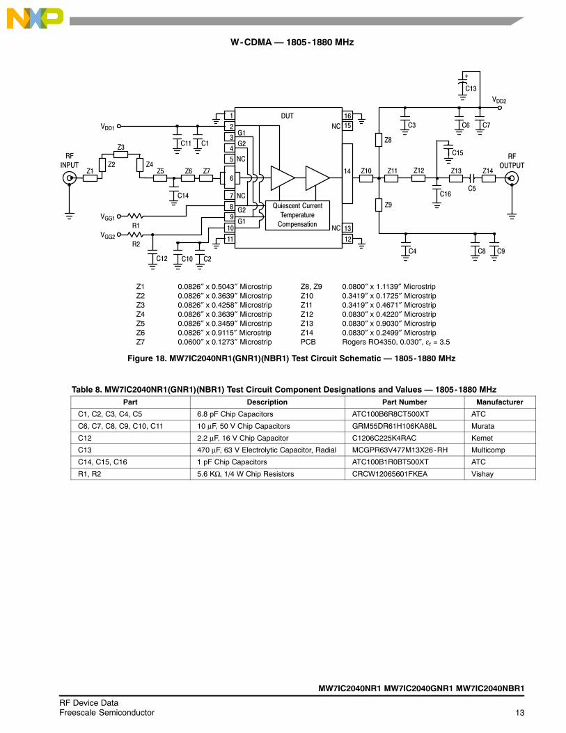
W-CDMA � 1805-1880 MHz
Z8, Z9 0.0800″ x 1.1139″ MicrostripZ10 0.3419″ x 0.1725″ MicrostripZ11 0.3419″ x 0.4671″ MicrostripZ12 0.0830″ x 0.4220″ MicrostripZ13 0.0830″ x 0.9030″ MicrostripZ14 0.0830″ x 0.2499″ MicrostripPCB Rogers RO4350, 0.030″, εr = 3.5
Z1 0.0826″ x 0.5043″ MicrostripZ2 0.0826″ x 0.3639″ MicrostripZ3 0.0826″ x 0.4258″ MicrostripZ4 0.0826″ x 0.3639″ MicrostripZ5 0.0826″ x 0.3459″ MicrostripZ6 0.0826″ x 0.9115″ MicrostripZ7 0.0600″ x 0.1273″ Microstrip
Figure 18. MW7IC2040NR1(GNR1)(NBR1) Test Circuit Schematic � 1805-1880 MHz
R1
RF
INPUT
VGG1
Z10
RF
OUTPUT
C5
C3
VDD2
1
2
3
4
5
6
7
8
14
13
1211
10
9
15
16DUT
Z6
C1
VDD1
Z8
Quiescent Current
Temperature
Compensation
Z1
Z9
Z11 Z12
C11
VGG2
C12 C10 C2
Z13
C6
C13
+
C4 C8 C9
Z7
C14
R2
C16
Z14
C7
Z2
Z3
Z4Z5
NC
NCG1
G2
NC
NC
G2
G1
C15
Table 8. MW7IC2040NR1(GNR1)(NBR1) Test Circuit Component Designations and Values � 1805-1880 MHzPart Description Part Number Manufacturer
C1, C2, C3, C4, C5 6.8 pF Chip Capacitors ATC100B6R8CT500XT ATC
C6, C7, C8, C9, C10, C11 10 μF, 50 V Chip Capacitors GRM55DR61H106KA88L Murata
C12 2.2 μF, 16 V Chip Capacitor C1206C225K4RAC Kemet
C13 470 μF, 63 V Electrolytic Capacitor, Radial MCGPR63V477M13X26-RH Multicomp
C14, C15, C16 1 pF Chip Capacitors ATC100B1R0BT500XT ATC
R1, R2 5.6 KΩ, 1/4 W Chip Resistors CRCW12065601FKEA Vishay

14RF Device Data
Freescale Semiconductor
MW7IC2040NR1 MW7IC2040GNR1 MW7IC2040NBR1
W-CDMA � 1805-1880 MHz
Figure 19. MW7IC2040NR1(GNR1)(NBR1) Test Circuit Component Layout � 1805-1880 MHz
CU
T O
UT
AR
EA
C14
R1
R2
C12
C10
C2
C1
C11
C4
C8 C9
C16
C15
C5
C6 C7
C13
C3
MW7IC2040NRev. 2
TO272WB−16
MW7IC2040NR1 MW7IC2040GNR1 MW7IC2040NBR1
15RF Device DataFreescale Semiconductor
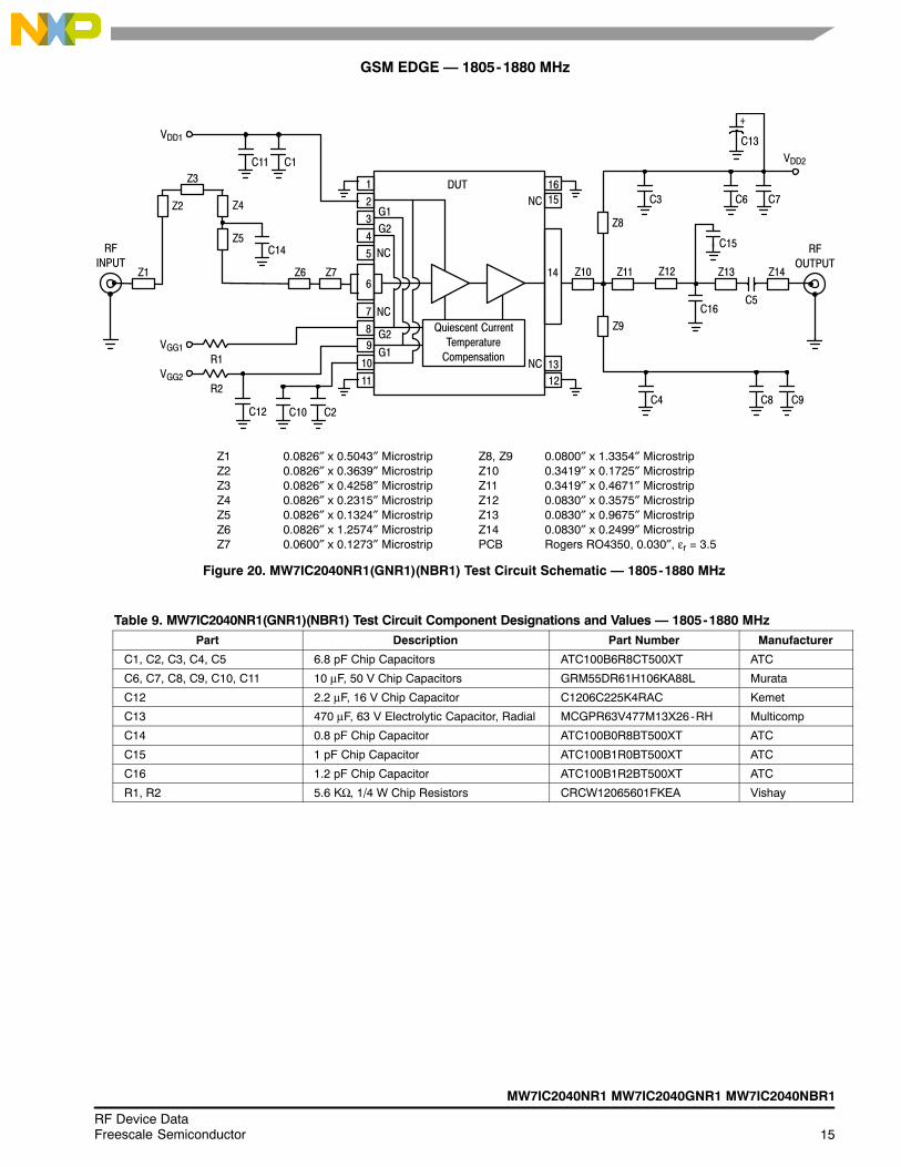
GSM EDGE � 1805-1880 MHz
Z8, Z9 0.0800″ x 1.3354″ MicrostripZ10 0.3419″ x 0.1725″ MicrostripZ11 0.3419″ x 0.4671″ MicrostripZ12 0.0830″ x 0.3575″ MicrostripZ13 0.0830″ x 0.9675″ MicrostripZ14 0.0830″ x 0.2499″ MicrostripPCB Rogers RO4350, 0.030″, εr = 3.5
Z1 0.0826″ x 0.5043″ MicrostripZ2 0.0826″ x 0.3639″ MicrostripZ3 0.0826″ x 0.4258″ MicrostripZ4 0.0826″ x 0.2315″ MicrostripZ5 0.0826″ x 0.1324″ MicrostripZ6 0.0826″ x 1.2574″ MicrostripZ7 0.0600″ x 0.1273″ Microstrip
Figure 20. MW7IC2040NR1(GNR1)(NBR1) Test Circuit Schematic � 1805-1880 MHz
R1
RF
INPUT
VGG1
Z10
RF
OUTPUT
C5
C3
VDD2
1
2
3
4
5
6
7
8
14
13
1211
10
9
15
16DUT
Z6
C1
VDD1
Z8
Quiescent Current
Temperature
Compensation
Z1
Z9
Z11 Z12
C11
VGG2
C12 C10 C2
Z13
C6
C13
+
C4 C8 C9
Z7
C14
R2
C16
Z14
C7Z2
Z3
Z4
NC
NCG1
G2
NC
NC
G2
G1
Z5 C15
Table 9. MW7IC2040NR1(GNR1)(NBR1) Test Circuit Component Designations and Values � 1805-1880 MHzPart Description Part Number Manufacturer
C1, C2, C3, C4, C5 6.8 pF Chip Capacitors ATC100B6R8CT500XT ATC
C6, C7, C8, C9, C10, C11 10 μF, 50 V Chip Capacitors GRM55DR61H106KA88L Murata
C12 2.2 μF, 16 V Chip Capacitor C1206C225K4RAC Kemet
C13 470 μF, 63 V Electrolytic Capacitor, Radial MCGPR63V477M13X26-RH Multicomp
C14 0.8 pF Chip Capacitor ATC100B0R8BT500XT ATC
C15 1 pF Chip Capacitor ATC100B1R0BT500XT ATC
C16 1.2 pF Chip Capacitor ATC100B1R2BT500XT ATC
R1, R2 5.6 KΩ, 1/4 W Chip Resistors CRCW12065601FKEA Vishay
16RF Device Data
Freescale Semiconductor
MW7IC2040NR1 MW7IC2040GNR1 MW7IC2040NBR1
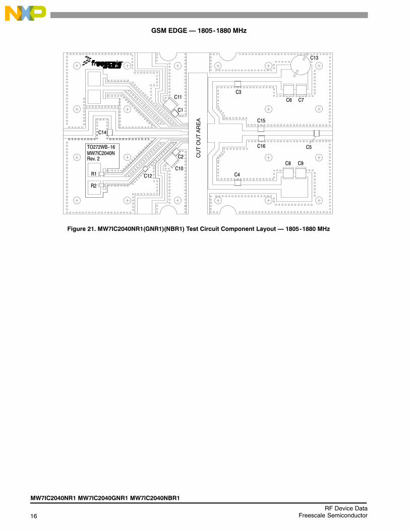
GSM EDGE � 1805-1880 MHz
Figure 21. MW7IC2040NR1(GNR1)(NBR1) Test Circuit Component Layout � 1805-1880 MHz
CU
T O
UT
AR
EA
C14
R1
R2
C12
C10
C2
C1
C11
C4
C8 C9
C16
C15
C5
C6 C7
C13
C3
MW7IC2040NRev. 2
TO272WB−16
MW7IC2040NR1 MW7IC2040GNR1 MW7IC2040NBR1
17RF Device DataFreescale Semiconductor
GSM EDGE � 1930-1990 MHz
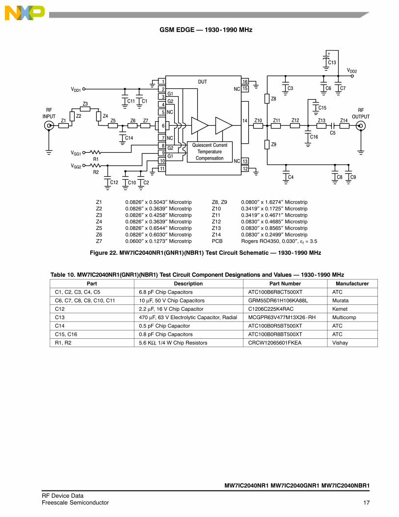
Z8, Z9 0.0800″ x 1.6274″ MicrostripZ10 0.3419″ x 0.1725″ MicrostripZ11 0.3419″ x 0.4671″ MicrostripZ12 0.0830″ x 0.4685″ MicrostripZ13 0.0830″ x 0.8565″ MicrostripZ14 0.0830″ x 0.2499″ MicrostripPCB Rogers RO4350, 0.030″, εr = 3.5
Z1 0.0826″ x 0.5043″ MicrostripZ2 0.0826″ x 0.3639″ MicrostripZ3 0.0826″ x 0.4258″ MicrostripZ4 0.0826″ x 0.3639″ MicrostripZ5 0.0826″ x 0.6544″ MicrostripZ6 0.0826″ x 0.6030″ MicrostripZ7 0.0600″ x 0.1273″ Microstrip
Figure 22. MW7IC2040NR1(GNR1)(NBR1) Test Circuit Schematic � 1930-1990 MHz
R1
RF
INPUT
VGG1
Z10
RF
OUTPUT
C5
C3
VDD2
1
2
3
4
5
6
7
8
14
13
1211
10
9
15
16DUT
Z6
C1
VDD1
Z8
Quiescent Current
Temperature
Compensation
Z1
Z9
Z11 Z12
C11
VGG2
C12 C10 C2
Z13
C6
C13
+
C4 C8 C9
Z7
C14
R2
C16
Z14
C7
Z2
Z3
Z4Z5
NC
NCG1
G2
NC
NC
G2
G1
C15
Table 10. MW7IC2040NR1(GNR1)(NBR1) Test Circuit Component Designations and Values � 1930-1990 MHzPart Description Part Number Manufacturer
C1, C2, C3, C4, C5 6.8 pF Chip Capacitors ATC100B6R8CT500XT ATC
C6, C7, C8, C9, C10, C11 10 μF, 50 V Chip Capacitors GRM55DR61H106KA88L Murata
C12 2.2 μF, 16 V Chip Capacitor C1206C225K4RAC Kemet
C13 470 μF, 63 V Electrolytic Capacitor, Radial MCGPR63V477M13X26-RH Multicomp
C14 0.5 pF Chip Capacitor ATC100B0R5BT500XT ATC
C15, C16 0.8 pF Chip Capacitors ATC100B0R8BT500XT ATC
R1, R2 5.6 KΩ, 1/4 W Chip Resistors CRCW12065601FKEA Vishay

18RF Device Data
Freescale Semiconductor
MW7IC2040NR1 MW7IC2040GNR1 MW7IC2040NBR1
GSM EDGE � 1930-1990 MHz
Figure 23. MW7IC2040NR1(GNR1)(NBR1) Test Circuit Component Layout � 1930-1990 MHz
CU
T O
UT
AR
EA
C14
R1
R2
C12
C10
C2
C1
C11
C4
C8 C9
C16
C15
C5
C6 C7
C13
C3
MW7IC2040NRev. 2
TO272WB−16
MW7IC2040NR1 MW7IC2040GNR1 MW7IC2040NBR1
19RF Device DataFreescale Semiconductor
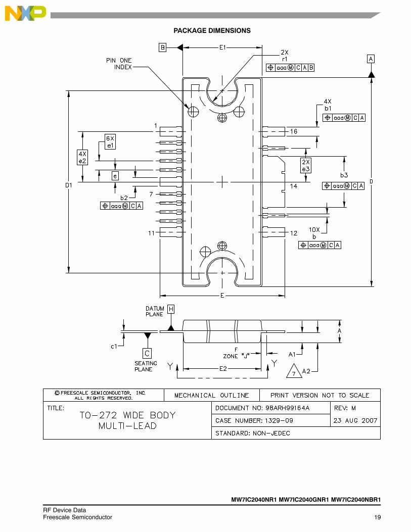
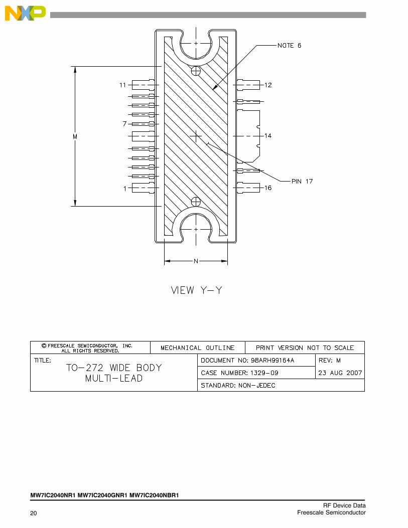
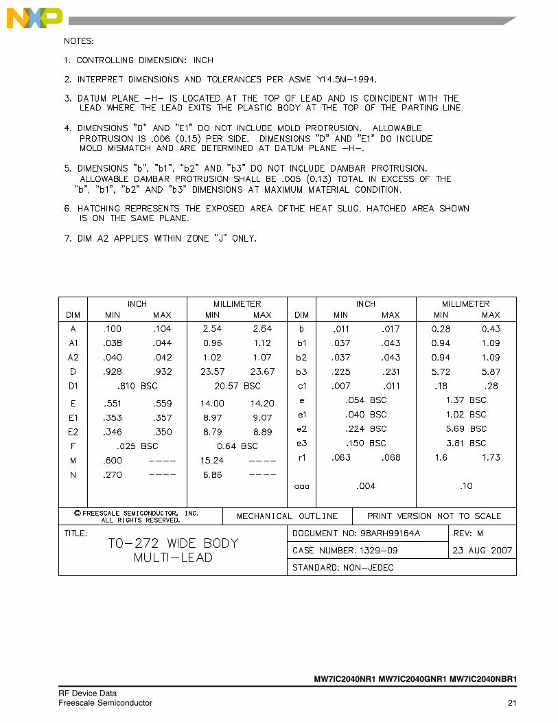
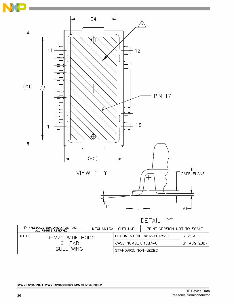
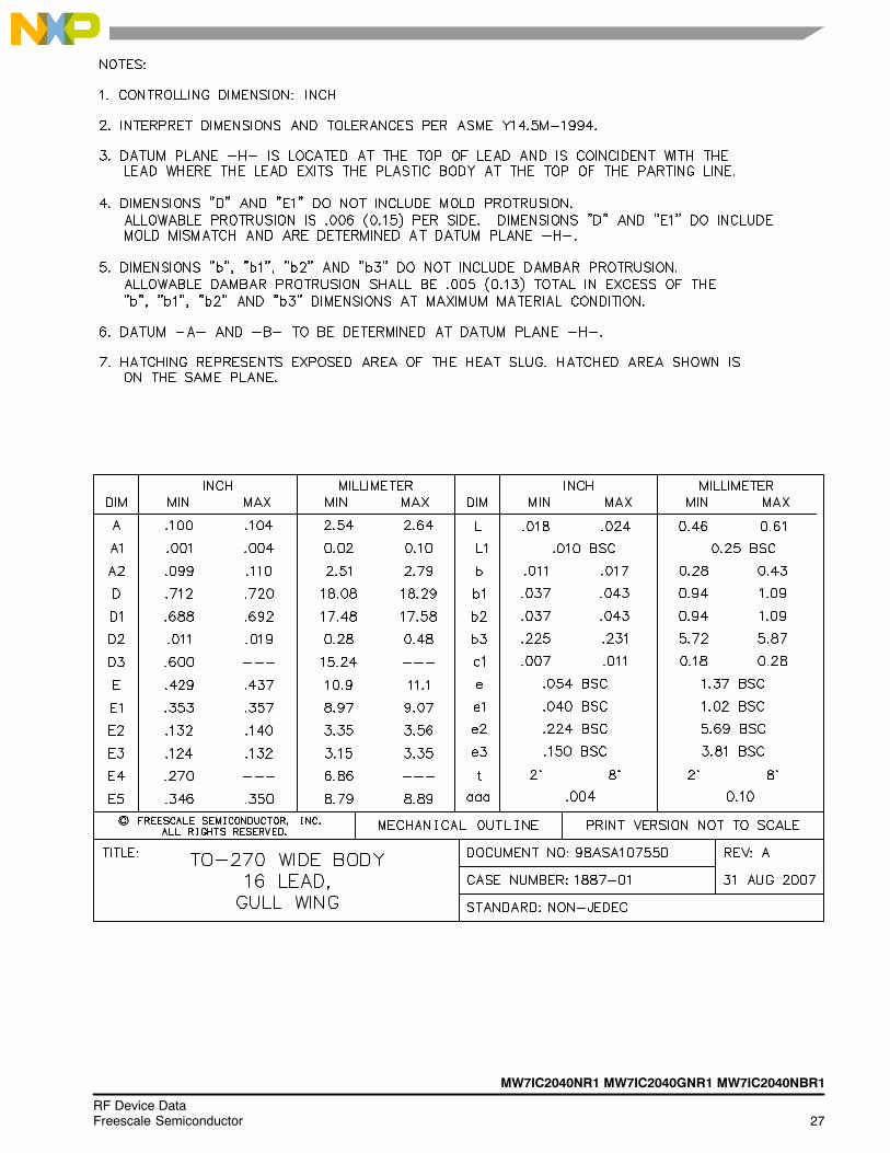
PACKAGE DIMENSIONS
20RF Device Data
Freescale Semiconductor
MW7IC2040NR1 MW7IC2040GNR1 MW7IC2040NBR1
MW7IC2040NR1 MW7IC2040GNR1 MW7IC2040NBR1
21RF Device DataFreescale Semiconductor
22RF Device Data
Freescale Semiconductor
MW7IC2040NR1 MW7IC2040GNR1 MW7IC2040NBR1
MW7IC2040NR1 MW7IC2040GNR1 MW7IC2040NBR1
23RF Device DataFreescale Semiconductor
24RF Device Data
Freescale Semiconductor
MW7IC2040NR1 MW7IC2040GNR1 MW7IC2040NBR1
MW7IC2040NR1 MW7IC2040GNR1 MW7IC2040NBR1
25RF Device DataFreescale Semiconductor
26RF Device Data
Freescale Semiconductor
MW7IC2040NR1 MW7IC2040GNR1 MW7IC2040NBR1
MW7IC2040NR1 MW7IC2040GNR1 MW7IC2040NBR1
27RF Device DataFreescale Semiconductor
28RF Device Data
Freescale Semiconductor
MW7IC2040NR1 MW7IC2040GNR1 MW7IC2040NBR1
PRODUCT DOCUMENTATION, TOOLS AND SOFTWARE
Refer to the following documents to aid your design process.
Application Notes
• AN1907: Solder Reflow Attach Method for High Power RF Devices in Plastic Packages
• AN1955: Thermal Measurement Methodology of RF Power Amplifiers
• AN1977: Quiescent Current Thermal Tracking Circuit in the RF Integrated Circuit Family
• AN1987: Quiescent Current Control for the RF Integrated Circuit Device Family
• AN3263: Bolt Down Mounting Method for High Power RF Transistors and RFICs in Over-Molded Plastic Packages
• AN3789: Clamping of High Power RF Transistors and RFICs in Over-Molded Plastic Packages
Engineering Bulletins• EB212: Using Data Sheet Impedances for RF LDMOS Devices
Software• Electromigration MTTF Calculator
• RF High Power Model
For Software and Tools, do a Part Number search at http://www.freescale.com, and select the �Part Number� link. Go to theSoftware & Tools tab on the part�s Product Summary page to download the respective tool.
REVISION HISTORY
The following table summarizes revisions to this document.
Revision Date Description
0 Feb. 2009 • Initial Release of Data Sheet
1 Nov. 2009 • Updated Human Body Model ESD from Class 1C to 1B to reflect Human Body Model actual test data,p. 2
• Fig. 13, CCDF W-CDMA 3GPP, Test Model 1, 64 DPCH, 45.2% Clipping, Single-Carrier Test Signal andFig. 14, Single-Carrier W-CDMA Spectrum updated to show the undistorted input test signal, p. 9
• Added AN3789, Clamping of High Power RF Transistors and RFICs in Over-Molded Plastic Packages toProduct Documentation, Application Notes, p. 28
• Added Electromigration MTTF Calculator and RF High Power Model availability to Product Software,p. 28
MW7IC2040NR1 MW7IC2040GNR1 MW7IC2040NBR1
29RF Device DataFreescale Semiconductor
Information in this document is provided solely to enable system and softwareimplementers to use Freescale Semiconductor products. There are no express orimplied copyright licenses granted hereunder to design or fabricate any integratedcircuits or integrated circuits based on the information in this document.
Freescale Semiconductor reserves the right to make changes without further notice toany products herein. Freescale Semiconductor makes no warranty, representation orguarantee regarding the suitability of its products for any particular purpose, nor doesFreescale Semiconductor assume any liability arising out of the application or use ofany product or circuit, and specifically disclaims any and all liability, including withoutlimitation consequential or incidental damages. �Typical� parameters that may beprovided in Freescale Semiconductor data sheets and/or specifications can and dovary in different applications and actual performance may vary over time. All operatingparameters, including �Typicals�, must be validated for each customer application bycustomer�s technical experts. Freescale Semiconductor does not convey any licenseunder its patent rights nor the rights of others. Freescale Semiconductor products arenot designed, intended, or authorized for use as components in systems intended forsurgical implant into the body, or other applications intended to support or sustain life,or for any other application in which the failure of the Freescale Semiconductor productcould create a situation where personal injury or death may occur. Should Buyerpurchase or use Freescale Semiconductor products for any such unintended orunauthorized application, Buyer shall indemnify and hold Freescale Semiconductorand its officers, employees, subsidiaries, affiliates, and distributors harmless against allclaims, costs, damages, and expenses, and reasonable attorney fees arising out of,directly or indirectly, any claim of personal injury or death associated with suchunintended or unauthorized use, even if such claim alleges that FreescaleSemiconductor was negligent regarding the design or manufacture of the part.
Freescale� and the Freescale logo are trademarks of Freescale Semiconductor, Inc.All other product or service names are the property of their respective owners.© Freescale Semiconductor, Inc. 2009. All rights reserved.
How to Reach Us:
Home Page:www.freescale.com
Web Support:http://www.freescale.com/support
USA/Europe or Locations Not Listed:Freescale Semiconductor, Inc.Technical Information Center, EL5162100 East Elliot RoadTempe, Arizona 852841-800-521-6274 or +1-480-768-2130www.freescale.com/support
Europe, Middle East, and Africa:Freescale Halbleiter Deutschland GmbHTechnical Information CenterSchatzbogen 781829 Muenchen, Germany+44 1296 380 456 (English)+46 8 52200080 (English)+49 89 92103 559 (German)+33 1 69 35 48 48 (French)www.freescale.com/support
Japan:Freescale Semiconductor Japan Ltd.HeadquartersARCO Tower 15F1-8-1, Shimo-Meguro, Meguro-ku,Tokyo 153-0064Japan0120 191014 or +81 3 5437 [email protected]
Asia/Pacific:Freescale Semiconductor China Ltd.Exchange Building 23FNo. 118 Jianguo RoadChaoyang DistrictBeijing 100022 China +86 10 5879 [email protected]
For Literature Requests Only:Freescale Semiconductor Literature Distribution Center1-800-441-2447 or +1-303-675-2140Fax: [email protected]
Document Number: MW7IC2040NRev. 1, 11/2009