Protective Relay Platform - CSE Uniserve
516
Communications Guide 8 Series version: 1.6x GE publication code: 1601-0702-A2 (GEK-130907A) *1601-0702-A2* 8 Series Protective Relay Platform 850 - 845 - 869 - 889 GE Grid Solutions
Transcript of Protective Relay Platform - CSE Uniserve

Communications Guide8 Series version: 1.6x
GE publication code: 1601-0702-A2 (GEK-130907A)
*1601-0702-A2*
8 SeriesProtective Relay Platform
850 - 845 - 869 - 889
GEGrid Solutions

© 2016 GE Multilin Inc. Incorporated. All rights reserved.
GE Multilin Inc. 8 Series Protective Relay Platform Communications Guide for revision 1.6x.
8 Series Protective Relay Platform, EnerVista, EnerVista Launchpad, and EnerVista 8 Series Setup are registered trademarks of GE Multilin Inc.
The contents of this manual are the property of GE Multilin Inc. This documentation is furnished on license and may not be reproduced in whole or in part without the permission of GE Multilin Inc. The content of this manual is for informational use only and is subject to change without notice.
Part number: 1601-0702-A2 (April 2016)
Table of Contents
1.INTRODUCTION 1 - 1Communications .............................................................................................................................. 1 - 1
For Further Assistance ............................................................................................................................1 - 2
2.COMMUNICATION PORTS 2 - 1RS485 Port ........................................................................................................................................... 2 - 1
RS485 ..............................................................................................................................................................2 - 1WiFi ......................................................................................................................................................... 2 - 2
WiFi Quick Start Procedure...................................................................................................................2 - 4USB.......................................................................................................................................................... 2 - 5
Using the Quick Connect Feature via the USB Port...................................................................2 - 5Ethernet Ports .................................................................................................................................... 2 - 6
Network Settings Menu ..........................................................................................................................2 - 6Routing ...........................................................................................................................................................2 - 8
3.TIME PROTOCOLS 3 - 1Real-time Clock ................................................................................................................................. 3 - 1
IEEE 1588 Precision Time Protocol (PTP) .........................................................................................3 - 1PTP Status......................................................................................................................................................3 - 1PTP Configuration ......................................................................................................................................3 - 3
Clock ................................................................................................................................................................3 - 4IRIG-B...............................................................................................................................................................3 - 5
4.DNP PROTOCOL 4 - 1DNP communication ...................................................................................................................... 4 - 3DNP device profile ........................................................................................................................... 4 - 7DNP implementation ....................................................................................................................4 - 10
5.DNP / IEC104 POINT LISTS 5 - 1
6.IEC 60870-5-104 6 - 1Interoperability.................................................................................................................................. 6 - 2
7.IEC 60870-5-103 7 - 1Cause of Transmission .................................................................................................................. 7 - 1Communications Menus............................................................................................................... 7 - 2Interoperability.................................................................................................................................. 7 - 4
Physical layer..............................................................................................................................................7 - 4Electrical interface.....................................................................................................................................7 - 4Optical interface.........................................................................................................................................7 - 4Transmission speed..................................................................................................................................7 - 4
Link layer .......................................................................................................................................................7 - 4Application layer........................................................................................................................................7 - 5
Transmission mode for application data........................................................................................7 - 5Common address of ASDU....................................................................................................................7 - 5Selection of standard information numbers in monitor direction......................................7 - 5Selection of standard information numbers in control direction........................................7 - 7
8 SERIES PROTECTIVE RELAY PLATFORM – COMMUNICATIONS GUIDE TOC-1
Basic application functions.................................................................................................................. 7 - 8Miscellaneous ............................................................................................................................................. 7 - 8
8.IEC 61850 8 - 1General ..................................................................................................................................................8 - 1Functionality .......................................................................................................................................8 - 4The IEC 61850 Configurator.........................................................................................................8 - 5
Online and Offline Setup........................................................................................................................ 8 - 5IEC 61850 Configurator Details .......................................................................................................... 8 - 7
ICD/CID........................................................................................................................................................... 8 - 7Settings.......................................................................................................................................................... 8 - 9Reports.........................................................................................................................................................8 - 12Goose Transmission ..............................................................................................................................8 - 17Goose Reception .....................................................................................................................................8 - 22
9.FILE TRANSFER PROTOCOLS 9 - 1
10.MODBUS PROTOCOL 10 - 1Modbus Protocol ............................................................................................................................ 10 - 2
Administrator Login and Commands via Modbus for 8 Series Relays ..........................10 - 7
11.MODBUS MEMORY MAP 11 - 1Reading the Event Recorder..................................................................................................... 11 - 1Reading Transient Recorder ..................................................................................................... 11 - 1Reading Fault Reports ................................................................................................................. 11 - 2Accessing Data via the User Map .......................................................................................... 11 - 2Memory Map Organization....................................................................................................... 11 - 3Using the Memory Map .............................................................................................................. 11 - 3
Reading CO Outputs ..............................................................................................................................11 - 3Interpreting Element Status for Breaker Contacts..................................................................11 - 4Reading Phase Current Values .........................................................................................................11 - 6
MODBUS memory map .............................................................................................................. 11 - 7Format Codes .............................................................................................................................11 - 226Modbus Commands ................................................................................................................11 - 409
A.845 RADIUS SERVER AND CERTIFICATES A - 1Simple RADIUS Server and Certificate Management.......................................................A - 1Setting Up a Simple RADIUS Server..........................................................................................A - 2
Radius Server Certificate Management ......................................................................................... A - 2Create a Private Key for the Server.................................................................................................. A - 2Create a Certificate Request for the Server.................................................................................. A - 2Create a Signed Certificate for the Server..................................................................................... A - 3
Radius Server Configuration................................................................................................................ A - 4Radius Client Configuration (8 Series Unit).................................................................................... A - 6
B.WARRANTY AND REVISION HISTORY B - 1Warranty ..............................................................................................................................................B - 1Revision history .................................................................................................................................B - 1
Major Updates............................................................................................................................................ B - 1
TOC-2 8 SERIES PROTECTIVE RELAY PLATFORM – COMMUNICATIONS GUIDE
8 Series Protective Relay Platform
Chapter 1: Introduction
GEGrid Solutions
Introduction
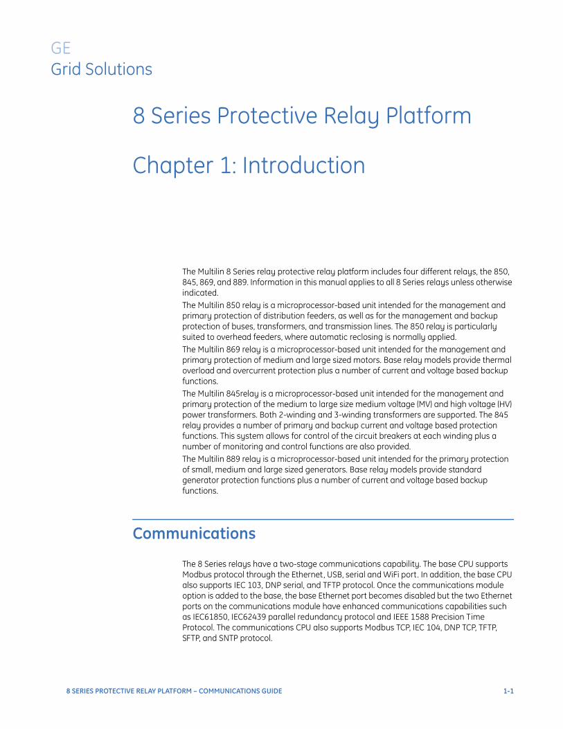
The Multilin 8 Series relay protective relay platform includes four different relays, the 850, 845, 869, and 889. Information in this manual applies to all 8 Series relays unless otherwise indicated.The Multilin 850 relay is a microprocessor-based unit intended for the management and primary protection of distribution feeders, as well as for the management and backup protection of buses, transformers, and transmission lines. The 850 relay is particularly suited to overhead feeders, where automatic reclosing is normally applied.The Multilin 869 relay is a microprocessor-based unit intended for the management and primary protection of medium and large sized motors. Base relay models provide thermal overload and overcurrent protection plus a number of current and voltage based backup functions.The Multilin 845relay is a microprocessor-based unit intended for the management and primary protection of the medium to large size medium voltage (MV) and high voltage (HV) power transformers. Both 2-winding and 3-winding transformers are supported. The 845 relay provides a number of primary and backup current and voltage based protection functions. This system allows for control of the circuit breakers at each winding plus a number of monitoring and control functions are also provided.The Multilin 889 relay is a microprocessor-based unit intended for the primary protection of small, medium and large sized generators. Base relay models provide standard generator protection functions plus a number of current and voltage based backup functions.
Communications
The 8 Series relays have a two-stage communications capability. The base CPU supports Modbus protocol through the Ethernet, USB, serial and WiFi port. In addition, the base CPU also supports IEC 103, DNP serial, and TFTP protocol. Once the communications module option is added to the base, the base Ethernet port becomes disabled but the two Ethernet ports on the communications module have enhanced communications capabilities such as IEC61850, IEC62439 parallel redundancy protocol and IEEE 1588 Precision Time Protocol. The communications CPU also supports Modbus TCP, IEC 104, DNP TCP, TFTP, SFTP, and SNTP protocol.
8 SERIES PROTECTIVE RELAY PLATFORM – COMMUNICATIONS GUIDE 1-1

COMMUNICATIONS CHAPTER 1: INTRODUCTION
For Further AssistanceFor product support, contact the information and call center as follows:GE Grid Solutions650 Markland StreetMarkham, OntarioCanada L6C 0M1Worldwide telephone: +1 905 927 7070Europe/Middle East/Africa telephone: +34 94 485 88 54North America toll-free: 1 800 547 8629Fax: +1 905 927 5098Worldwide e-mail: [email protected] e-mail: [email protected]: http://www.gegridsolutions.com/multilin/
1-2 8 SERIES PROTECTIVE RELAY PLATFORM – COMMUNICATIONS GUIDE
8 Series Protective Relay Platform
Chapter 2: Communication Ports
GEGrid Solutions
Communication Ports
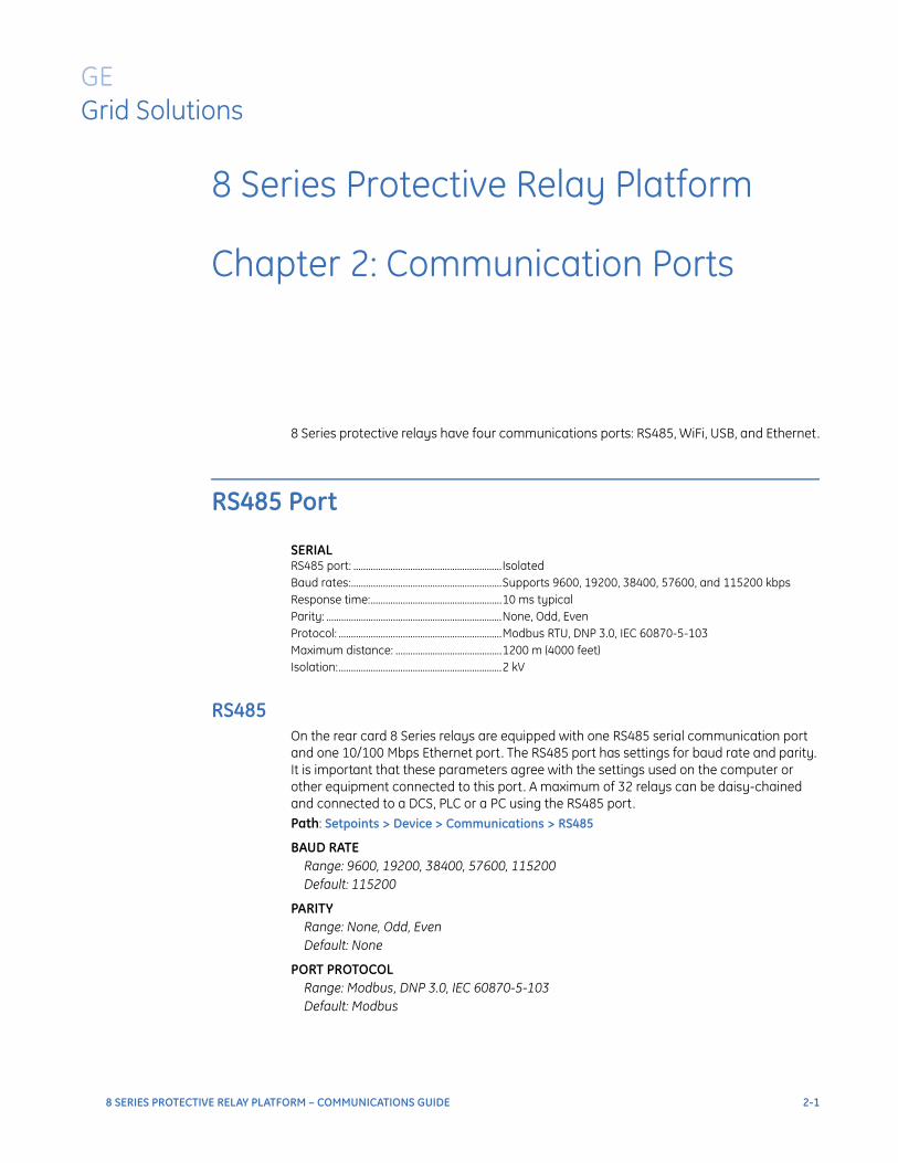
8 Series protective relays have four communications ports: RS485, WiFi, USB, and Ethernet.
RS485 Port
SERIALRS485 port: ............................................................IsolatedBaud rates:.............................................................Supports 9600, 19200, 38400, 57600, and 115200 kbpsResponse time:.....................................................10 ms typicalParity: .......................................................................None, Odd, EvenProtocol: ..................................................................Modbus RTU, DNP 3.0, IEC 60870-5-103Maximum distance: ...........................................1200 m (4000 feet)Isolation:..................................................................2 kV
RS485On the rear card 8 Series relays are equipped with one RS485 serial communication port and one 10/100 Mbps Ethernet port. The RS485 port has settings for baud rate and parity. It is important that these parameters agree with the settings used on the computer or other equipment connected to this port. A maximum of 32 relays can be daisy-chained and connected to a DCS, PLC or a PC using the RS485 port.Path: Setpoints > Device > Communications > RS485
BAUD RATERange: 9600, 19200, 38400, 57600, 115200Default: 115200
PARITYRange: None, Odd, EvenDefault: None
PORT PROTOCOLRange: Modbus, DNP 3.0, IEC 60870-5-103Default: Modbus
8 SERIES PROTECTIVE RELAY PLATFORM – COMMUNICATIONS GUIDE 2-1
WIFI CHAPTER 2: COMMUNICATION PORTS
WiFi
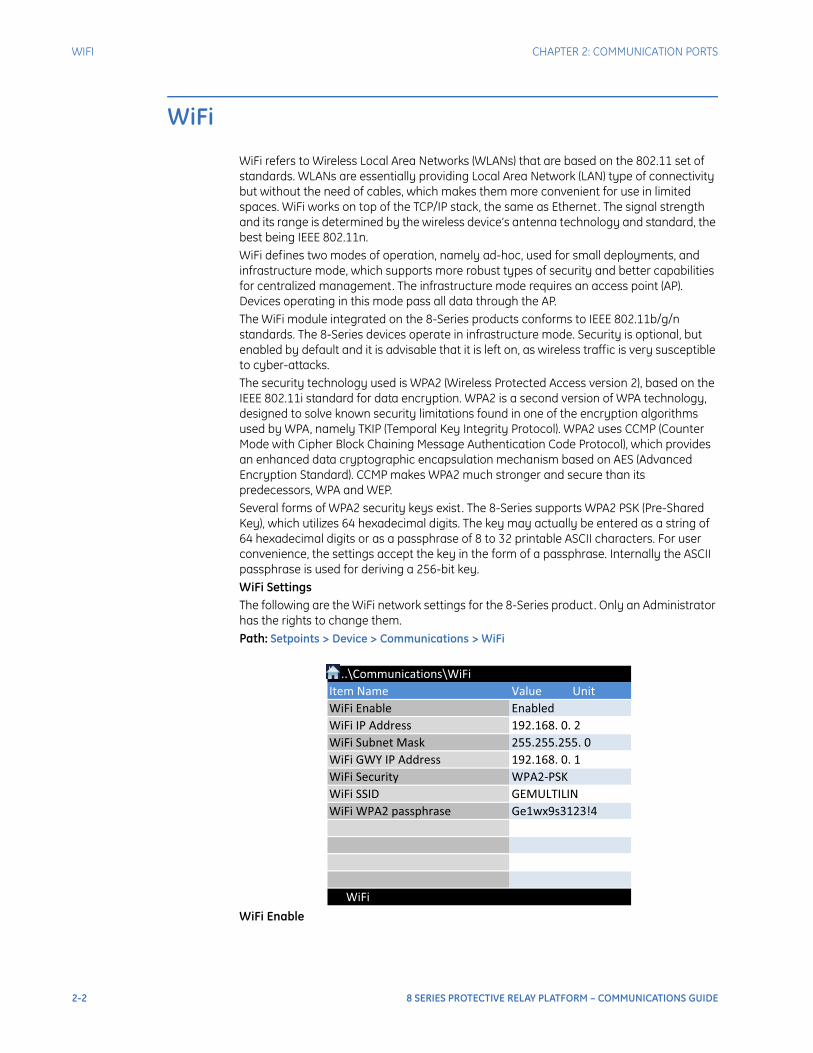
WiFi refers to Wireless Local Area Networks (WLANs) that are based on the 802.11 set of standards. WLANs are essentially providing Local Area Network (LAN) type of connectivity but without the need of cables, which makes them more convenient for use in limited spaces. WiFi works on top of the TCP/IP stack, the same as Ethernet. The signal strength and its range is determined by the wireless device’s antenna technology and standard, the best being IEEE 802.11n.WiFi defines two modes of operation, namely ad-hoc, used for small deployments, and infrastructure mode, which supports more robust types of security and better capabilities for centralized management. The infrastructure mode requires an access point (AP). Devices operating in this mode pass all data through the AP. The WiFi module integrated on the 8-Series products conforms to IEEE 802.11b/g/n standards. The 8-Series devices operate in infrastructure mode. Security is optional, but enabled by default and it is advisable that it is left on, as wireless traffic is very susceptible to cyber-attacks.The security technology used is WPA2 (Wireless Protected Access version 2), based on the IEEE 802.11i standard for data encryption. WPA2 is a second version of WPA technology, designed to solve known security limitations found in one of the encryption algorithms used by WPA, namely TKIP (Temporal Key Integrity Protocol). WPA2 uses CCMP (Counter Mode with Cipher Block Chaining Message Authentication Code Protocol), which provides an enhanced data cryptographic encapsulation mechanism based on AES (Advanced Encryption Standard). CCMP makes WPA2 much stronger and secure than its predecessors, WPA and WEP.Several forms of WPA2 security keys exist. The 8-Series supports WPA2 PSK (Pre-Shared Key), which utilizes 64 hexadecimal digits. The key may actually be entered as a string of 64 hexadecimal digits or as a passphrase of 8 to 32 printable ASCII characters. For user convenience, the settings accept the key in the form of a passphrase. Internally the ASCII passphrase is used for deriving a 256-bit key.WiFi SettingsThe following are the WiFi network settings for the 8-Series product. Only an Administrator has the rights to change them.Path: Setpoints > Device > Communications > WiFi
WiFi Enable
..\Communications\WiFiItem Name Value UnitWiFi Enable EnabledWiFi IP Address 192.168. 0. 2WiFi Subnet Mask 255.255.255. 0WiFi GWY IP Address 192.168. 0. 1WiFi Security WPA2-PSKWiFi SSID GEMULTILINWiFi WPA2 passphrase Ge1wx9s3123!4
WiFi
2-2 8 SERIES PROTECTIVE RELAY PLATFORM – COMMUNICATIONS GUIDE

CHAPTER 2: COMMUNICATION PORTS WIFI
This setting switches WiFi functionality on/off. By default WiFi is enabled in the basic offering, but it is disabled in software options that offer CyberSentry.WiFi IP Address / Subnet MaskThe default IP address is 192.168.0.x, where x is calculated as:X = (modulo 242 of the last 3 digits of the serial number) + 12This is to ensure uniqueness of the default IP address for all 8 Series devices present on one wireless network and it creates a usable address space from 192.168.0.12 to 192.168.0.253 for 8 Series devices.
NOTE
NOTE: From the remaining range of unicast addresses 192.168.0.1 to 192.168.0.11, at least two are going to be used for the AP and a laptop installed with the EnerVista software, which will be used to configure the 8 Series devices. The AP should be configured with the address 192.168.0.1 and mask 255.255.255.0 and have DHCP enabled with a DHCP range from 192.168.0.2 to 192.168.0.11. This allows laptops, iPads and any other devices (Android, iPhone) to connect to the local network without the need to statically configure their own IP address and mask.
WiFi GWY IP AddressThe setting specifies the address of the access point AP which the 8 Series device uses for communicating over WiFi.WiFi SecurityThe setting enables WiFi security. If set to “None”, there is no security and all traffic is open. By default WiFi Security is set to WPA2-PSK.WiFi SSIDThe SSID is the public name of a wireless network. All of the wireless devices on a WLAN must use the same SSID in order to communicate with each other. The default for the SSID is provided by the vendor with the shipment of any new 8-Series device. It is recommended that the customer modifies this name as needed after initial startup, to ensure unique SSIDs if several WLANs are configured.
NOTE
NOTE: SSID broadcast should be disabled on AP. This provides some extra protection by requiring a user to know an SSID before the user can connect to the device and making it harder for casual outsiders looking for wireless networks to find the device and attempt to connect.
WiFi WPA2 PassphraseThe WPA2 Passphrase is used for generating the encryption key. The same passphrase must be set on AP and on all devices communicating on the same WLAN. The 8-Series device supports a string of up to 14 printable ASCII characters. Internally a 256-bit key is calculated by applying the PBKDF2 key derivation function to this passphrase, using the SSID as the salt and 4096 iterations of HMAC-SHA1.The 8-Series devices are configured with a default passphrase, which is provided by the vendor with the shipment of any new 8-Series device.When choosing a new passphrase, the password complexity rules of CyberSentry must be used (see CyberSentry details in the relay Instruction manual).This field is visible only if the security is set to WPA2-PSK.
NOTE
NOTE: Ideally the passphrase should be set through EnerVista and not directly from the Keypad, where there are limitations in terms of space and types of characters supported. However, for convenience, the key setting is available from the Keypad as well.
WiFi StatusA WiFi symbol is displayed in the caption area of the 8-Series product front panel. The following table lists all possibilities for this icon:
8 SERIES PROTECTIVE RELAY PLATFORM – COMMUNICATIONS GUIDE 2-3
WIFI CHAPTER 2: COMMUNICATION PORTS
WiFi Events
NOTE
NOTE: If the relay is in service mode and the settings are default a minor error is triggered.
WiFi Quick Start ProcedureThe following provides the settings information and instructions to quickly setup WiFi.Required Equipment
• 8-Series Relay with WiFi functionality
• PC with WiFi
• Access Point
Quick Start Procedure
1. The PC WiFi Network Settings are as follows: Passphrase: provided with the 8-Series relay
2. The Access Point Settings are given below:
3. If the 8-Series relay(s) are in range, they automatically connect to the configured Access Point.
4. Start EnerVista on a PC and use the Discover function, all relays within range appear and are populated in Enervista for initial configuration and commissioning.
5. Once the relay is configured, change the 8-Series relay default WiFi SSID and Passphrase settings before the relay goes into service.
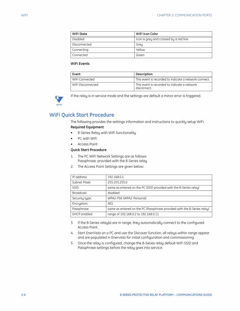
WiFi State WiFi Icon Color
Disabled Icon is grey and crossed by a red line
Disconnected Grey
Connecting Yellow
Connected Green
Event Description
WiFi Connected This event is recorded to indicate a network connect.
WiFi Disconnected This event is recorded to indicate a network disconnect.
IP address: 192.168.0.1
Subnet Mask: 255.255.255.0
SSID: same as entered on the PC (SSID provided with the 8-Series relay)
Broadcast disabled
Security type: WPA2-PSK (WPA2-Personal)
Encryption: AES
Passphrase: same as entered on the PC (Passphrase provided with the 8-Series relay)
DHCP enabled range of 192.168.0.2 to 192.168.0.11
2-4 8 SERIES PROTECTIVE RELAY PLATFORM – COMMUNICATIONS GUIDE
CHAPTER 2: COMMUNICATION PORTS USB
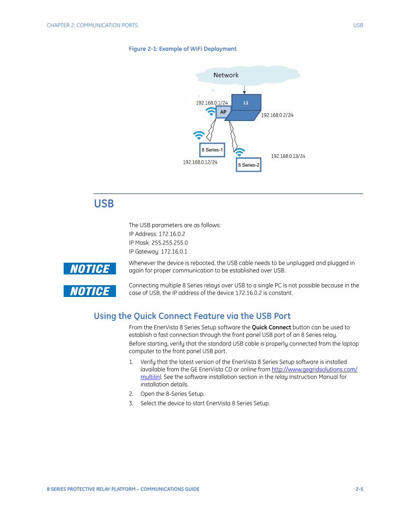
Figure 2-1: Example of WiFi Deployment
USB
The USB parameters are as follows:IP Address: 172.16.0.2IP Mask: 255.255.255.0IP Gateway: 172.16.0.1
FASTPATH: Whenever the device is rebooted, the USB cable needs to be unplugged and plugged in again for proper communication to be established over USB.
FASTPATH: Connecting multiple 8 Series relays over USB to a single PC is not possible because in the case of USB, the IP address of the device 172.16.0.2 is constant.
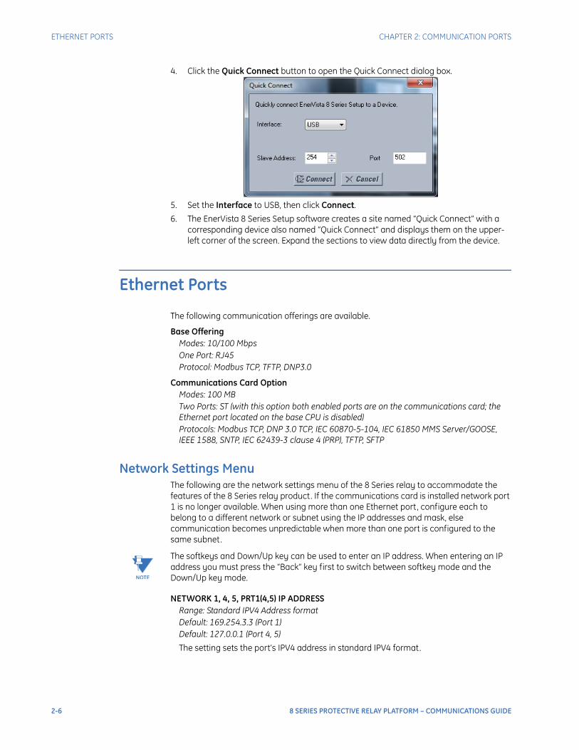
Using the Quick Connect Feature via the USB PortFrom the EnerVista 8 Series Setup software the Quick Connect button can be used to establish a fast connection through the front panel USB port of an 8 Series relay.Before starting, verify that the standard USB cable is properly connected from the laptop computer to the front panel USB port.
1. Verify that the latest version of the EnerVista 8 Series Setup software is installed (available from the GE EnerVista CD or online from http://www.gegridsolutions.com/multilin). See the software installation section in the relay Instruction Manual for installation details.
2. Open the 8-Series Setup.
3. Select the device to start EnerVista 8 Series Setup.
8 SERIES PROTECTIVE RELAY PLATFORM – COMMUNICATIONS GUIDE 2-5
ETHERNET PORTS CHAPTER 2: COMMUNICATION PORTS
4. Click the Quick Connect button to open the Quick Connect dialog box.
5. Set the Interface to USB, then click Connect.
6. The EnerVista 8 Series Setup software creates a site named “Quick Connect” with a corresponding device also named “Quick Connect” and displays them on the upper-left corner of the screen. Expand the sections to view data directly from the device.
Ethernet Ports
The following communication offerings are available.
Base OfferingModes: 10/100 MbpsOne Port: RJ45 Protocol: Modbus TCP, TFTP, DNP3.0
Communications Card OptionModes: 100 MBTwo Ports: ST (with this option both enabled ports are on the communications card; the Ethernet port located on the base CPU is disabled)Protocols: Modbus TCP, DNP 3.0 TCP, IEC 60870-5-104, IEC 61850 MMS Server/GOOSE, IEEE 1588, SNTP, IEC 62439-3 clause 4 (PRP), TFTP, SFTP
Network Settings MenuThe following are the network settings menu of the 8 Series relay to accommodate the features of the 8 Series relay product. If the communications card is installed network port 1 is no longer available. When using more than one Ethernet port, configure each to belong to a different network or subnet using the IP addresses and mask, else communication becomes unpredictable when more than one port is configured to the same subnet.
NOTE
NOTE: The softkeys and Down/Up key can be used to enter an IP address. When entering an IP address you must press the “Back” key first to switch between softkey mode and the Down/Up key mode.
NETWORK 1, 4, 5, PRT1(4,5) IP ADDRESSRange: Standard IPV4 Address formatDefault: 169.254.3.3 (Port 1)Default: 127.0.0.1 (Port 4, 5)
The setting sets the port’s IPV4 address in standard IPV4 format.
2-6 8 SERIES PROTECTIVE RELAY PLATFORM – COMMUNICATIONS GUIDE
CHAPTER 2: COMMUNICATION PORTS ETHERNET PORTS
NOTE
NOTE: The setting is valid on port 1 if the optional communications card is not present.
The setting is valid on port 5 if port 4’s OPERATION is set to INDEPENDENT.
PRT1(4,5) SUBNET IP MASKRange: Standard IPV4 mask formatDefault: 255.255.255.0 (Port 1)Default: 0.0.0.0 (Port 4, 5)
This setting specifies the IPv4 mask associated with the corresponding port IP address.
PRT1 GWY ADDRESS
This setting sets the ports IPv4 GATEWAY address in standard IPv4 format.
This setting is only valid on port 1.
This setting is not present on port 4 and 5, which are available on the communications card.
NOTE
NOTE: The communications card comes with the capability of setting a number of static routes and one default route, which is used instead of default gateways.
Notes:
• The fiber optic ports support only 100 Mbps.
• Changes to the Ethernet communications settings take effect only after rebooting the relay.
• All Ethernet ports have flex operands associated with them. A failure of one of the Ethernet ports will trigger an event, a target message and the corresponding operand set.
PRT4 OPERATIONRange: Independent, LLA, PRPDefault: Independent
This setting determines the mode of operation for ports 4 and 5: INDEPENDENT, LLA or PRP.
INDEPENDENT operation: ports 4 and 5 operate independently with their own MAC and IP address.
LLA operation: the operation of ports 4 and 5 are as follows:
Ports 4 and 5 use port 4’s MAC and IP address settings while port 5 is in standby mode in that it does not actively communicate on the Ethernet network but monitors its link. If Port 4 is active and the link loss problem is detected, communications is switched to Port 5 immediately. Port 5 is, in effect, acting as a redundant or backup link to the network for port 4.
LLA (Link Loss Alert) is a proprietary feature supported by the 8 Series relay fiber optic ports. When enabled on an 8 Series fiber optic port, this feature is able to detect a failure of the fiber link. If port 4’s OPERATION is set to LLA, the detection of a link failure by this feature triggers the transfer of communications from port 4 to port 5. If LLA is enabled on a port with a non-fiber SFP, the target message “LLA not supported by Prt (4 or 5)” is displayed on the keypad and an event is logged.
PRP (Parallel Redundancy Protocol): ports 4 and 5 use the same MAC address and combine information at the link layer. It is intended to only be used if the two ports are connected to separate parallel LAN’s. In this mode of operation both ports cannot be connected to the same LAN. The receiving devices (8 Series relay ) process the first frame received and discard the duplicate through a link redundancy entity (LRE) or similar service that operates below layer 2. Aside from LRE, PRP uses conventional Ethernet hardware but both ports must know they are in PRP. Ports of PRP devices
8 SERIES PROTECTIVE RELAY PLATFORM – COMMUNICATIONS GUIDE 2-7
ETHERNET PORTS CHAPTER 2: COMMUNICATION PORTS
operating with the same Internet Protocol (IP) addresses for traffic that uses IP Management protocols such as Address Resolution Protocol (ARP) must operate correctly.
Duplicate Discard mode (only mode supported by the 8 Series). This is the normal setting for PRP operation and once set it allows the sender LRE to append a six-octet field that contains a sequence number, the Redundancy Control Trailer (RCT) to both frames it sends. The receiver LRE uses the sequence number of the RCT and the source MAC address to detect duplicates. It forwards only the first frame of a pair to its upper layers.
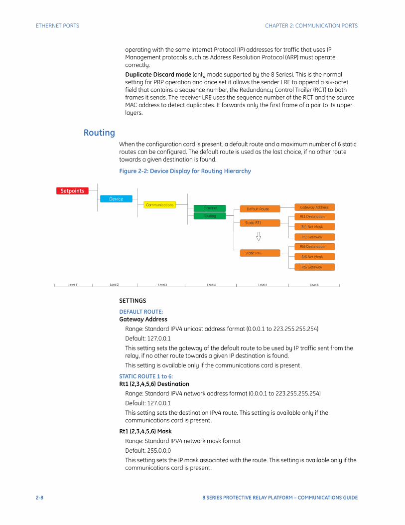
RoutingWhen the configuration card is present, a default route and a maximum number of 6 static routes can be configured. The default route is used as the last choice, if no other route towards a given destination is found.
Figure 2-2: Device Display for Routing Hierarchy
SETTINGS
DEFAULT ROUTE:Gateway Address
Range: Standard IPV4 unicast address format (0.0.0.1 to 223.255.255.254)
Default: 127.0.0.1
This setting sets the gateway of the default route to be used by IP traffic sent from the relay, if no other route towards a given IP destination is found.
This setting is available only if the communications card is present.
STATIC ROUTE 1 to 6: Rt1 (2,3,4,5,6) Destination
Range: Standard IPV4 network address format (0.0.0.1 to 223.255.255.254)
Default: 127.0.0.1
This setting sets the destination IPv4 route. This setting is available only if the communications card is present.
Rt1 (2,3,4,5,6) Mask
Range: Standard IPV4 network mask format
Default: 255.0.0.0
This setting sets the IP mask associated with the route. This setting is available only if the communications card is present.
2-8 8 SERIES PROTECTIVE RELAY PLATFORM – COMMUNICATIONS GUIDE

CHAPTER 2: COMMUNICATION PORTS ETHERNET PORTS
Rt1 (2,3,4,5,6) Gateway
Range: Standard IPV4 unicast address format (0.0.0.1 to 223.255.255.254)
Default: 127.0.0.1
This setting sets the destination IP route. This setting is available only if the communications card is present.
ADDING AND DELETING STATIC ROUTES
Defaults:
Rule #1. By default, the value of the destination field is 127.0.0.1 for all static routes (1 to 6). This is equivalent to saying that the static routes are not configured. When the destination address is 127.0.0.1, the mask and gateway must also be kept as default values.Rule #2. By default, the value of the default route gateway address is 127.0.0.1. This means the default route is not configured.
Adding a route:
Rule #3. Use any of the static network route entries numbered 1 to 6 to configure a static network route. Once a route destination is configured for any of the entries 1 to 6, that entry becomes a static route and it must meet all the rules listed in the following section under “Important Notes”.
Rule #4. To configure the default route, enter a default gateway address. A default gateway address configured must be validated against Rule #5, the next rule.
Deleting a route:
Rule #5. Routes are deleted by replacing the route destination with the default address (127.0.0.1). When deleting a route, the mask and gateway must also be put back to their default values.
Rule #6. The default route is deleted by replacing the default gateway with the default value 127.0.0.1.
Important Notes:
1. Host routes are not supported at present.
2. The route mask has IPv4 mask format. In binary this is a set of contiguous bits of 1 from left to right, followed by one or more contiguous bits of 0.
3. The route destination and mask must match.
4. Item #3, above, can be verified by checking that RtDestination & RtMask == RtDestination
5. This is an example of a good configuration: RtDestination= 10.1.1.0; Rt Mask= 255.255.255.0
6. This is an example of a bad configuration: RtDestination = 10.1.1.1; Rt Mask= 255.255.255.0
7. The route destination must not be a connected network.
8. The route gateway must be on a connected network. This rule applies to the gateway address of the default route as well.
9. Item #8, above, can be verified by checking that: RtGwy & Prt4Mask) == (Prt4IP & Prt4Mask) || (RtGwy & Prt5Mask) == (Prt5IP & Prt5Mask)
TARGETSWRONG ROUTE CONFIG
8 SERIES PROTECTIVE RELAY PLATFORM – COMMUNICATIONS GUIDE 2-9
ETHERNET PORTS CHAPTER 2: COMMUNICATION PORTS
Description: A route with mismatched destination and mask has been configured.Message: “Wrong route configuration.”What to do: Rectify the IP address and mask of the mis-configured route.
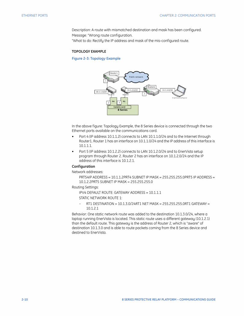
TOPOLOGY EXAMPLE
Figure 2-3: Topology Example
In the above figure: Topology Example, the 8 Series device is connected through the two Ethernet ports available on the communications card.
• Port 4 (IP address 10.1.1.2) connects to LAN 10.1.1.0/24 and to the Internet through Router1. Router 1 has an interface on 10.1.1.0/24 and the IP address of this interface is 10.1.1.1.
• Port 5 (IP address 10.1.2.2) connects to LAN 10.1.2.0/24 and to EnerVista setup program through Router 2. Router 2 has an interface on 10.1.2.0/24 and the IP address of this interface is 10.1.2.1.
ConfigurationNetwork addresses:
PRT54IP ADDRESS = 10.1.1.2PRT4 SUBNET IP MASK = 255.255.255.0PRT5 IP ADDRESS = 10.1.2.2PRT5 SUBNET IP MASK = 255.255.255.0
Routing Settings:IPV4 DEFAULT ROUTE: GATEWAY ADDRESS = 10.1.1.1STATIC NETWORK ROUTE 1:
– RT1 DESTINATION = 10.1.3.0/24RT1 NET MASK = 255.255.255.0RT1 GATEWAY = 10.1.2.1
Behavior: One static network route was added to the destination 10.1.3.0/24, where a laptop running EnerVista is located. This static route uses a different gateway (10.1.2.1) than the default route. This gateway is the address of Router 2, which is “aware” of destination 10.1.3.0 and is able to route packets coming from the 8 Series device and destined to EnerVista.
2-10 8 SERIES PROTECTIVE RELAY PLATFORM – COMMUNICATIONS GUIDE
8 Series Protective Relay Platform
Chapter 3: Time Protocols
GEGrid Solutions
Time Protocols
Real-time Clock
Path: Setpoints > Device > Real Time Clock
The 8 Series relay is capable of receiving a time reference from several time sources in addition to its own internal clock for the purpose of time-stamping events, transient recorders and other occurrences within the relay. The accuracy of the time stamp is based on the time reference that is used. The 8 Series relay supports an internal clock, SNTP, IRIG-B, and PTP IEEE 1588 as potential time references.If two or more time sources are available, the time source with the higher priority shown in Time Sources table is used where 1 is considered to be the highest priority. Please note that the time source priority of PTP and IRIG-B can be swapped. If both PTP and IRIG-B are available to the 8 Series relay, by default the 8 Series relay clock syncs to PTP over IRIG-B. If PTP is not available the 8 Series relay CPU syncs the internal clock to IRIG-B.
Table 3-1: Time Sources
* The priority of IRIG-B and PTP can be swapped.FASTPATH: Synchronization by IEC103, DNP, Modbus and IEC104 is not going to be issued if there is a
sync source from IRIG-B, SNTP or PTP.
IEEE 1588 Precision Time Protocol (PTP)
PTP Status The present values of the PTP protocol are displayed here.
Time Source Priority
PTP (IEEE1588) 1*
IRIG-B 2*
SNTP 3
Internal Clock 4
8 SERIES PROTECTIVE RELAY PLATFORM – COMMUNICATIONS GUIDE 3-1
REAL-TIME CLOCK CHAPTER 3: TIME PROTOCOLS
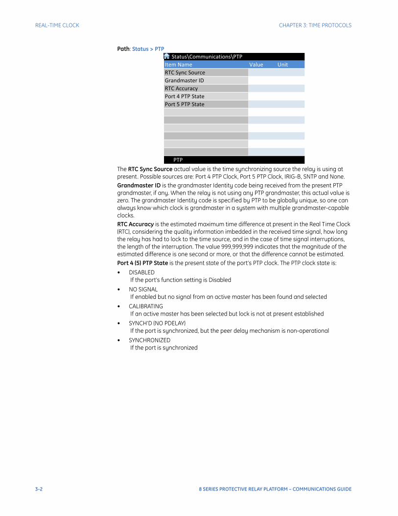
Path: Status > PTP
The RTC Sync Source actual value is the time synchronizing source the relay is using at present. Possible sources are: Port 4 PTP Clock, Port 5 PTP Clock, IRIG-B, SNTP and None.Grandmaster ID is the grandmaster Identity code being received from the present PTP grandmaster, if any. When the relay is not using any PTP grandmaster, this actual value is zero. The grandmaster Identity code is specified by PTP to be globally unique, so one can always know which clock is grandmaster in a system with multiple grandmaster-capable clocks.RTC Accuracy is the estimated maximum time difference at present in the Real Time Clock (RTC), considering the quality information imbedded in the received time signal, how long the relay has had to lock to the time source, and in the case of time signal interruptions, the length of the interruption. The value 999,999,999 indicates that the magnitude of the estimated difference is one second or more, or that the difference cannot be estimated.Port 4 (5) PTP State is the present state of the port’s PTP clock. The PTP clock state is:
• DISABLED If the port’s function setting is Disabled
• NO SIGNAL If enabled but no signal from an active master has been found and selected
• CALIBRATING If an active master has been selected but lock is not at present established
• SYNCH’D (NO PDELAY) If the port is synchronized, but the peer delay mechanism is non-operational
• SYNCHRONIZED If the port is synchronized
Status\Communications\PTPItem Name Value UnitRTC Sync SourceGrandmaster IDRTC AccuracyPort 4 PTP StatePort 5 PTP State
PTP
3-2 8 SERIES PROTECTIVE RELAY PLATFORM – COMMUNICATIONS GUIDE

CHAPTER 3: TIME PROTOCOLS REAL-TIME CLOCK
PTP Configuration Path: Setpoints > Device > Real Time Clock > Precision Time
PORT 4(5) PTP FUNCTIONRange: Disabled, EnabledDefault: Enabled
When the port setting is selected as “Disabled,” PTP is disabled on the port. The relay does not generate, or listen to, PTP messages on the port.
PORT 4(5) PATH DELAY ADDERRange: 0 to 60000 ns in steps of 1 nsDefault: 0 ns
The time delivered by PTP is advanced by the time value in the setting prior to the time being used to synchronize the relay’s real time clock. This is to compensate for time delivery delays not compensated for in the network. In a fully compliant Power Profile (PP) network, the peer delay and the processing delay mechanisms compensate for all the delays between the grandmaster and the relay. In such networks, the setting is zero.
In networks containing one or more switches and/or clocks that do not implement both of these mechanisms, not all delays are compensated, so the time of message arrival at the relay is later than the time indicated in the message. The setting can be used to approximately compensate for the delay. Since the relay is not aware of network switching that dynamically changes the amount of uncompensated delay, there is no setting that always completely corrects for uncompensated delay. A setting can be chosen that reduces worst-case error to half of the range between minimum and maximum uncompensated delay if these values are known.
PORT 4(5) PATH DELAY ASYMMETRYRange: -1000 to +1000 ns in steps of 1 nsDefault: 0 ns
The setting corresponds to “Delay Asymmetry” in PTP, which is used by the peer delay mechanism to compensate for any difference in the propagation delay between the two directions of a link. Except in unusual cases, the two fibers are of essentially identical length and composition, so the setting is set to zero.
In unusual cases where the length of link is different in different directions, the setting is to be set to the number of nanoseconds longer the Ethernet propagation delay is to the relay compared with the mean of path propagation delays to and from the relay. For instance, if it is known say from the physical length of the fibers and the propagation speed in the fibers that the delay from the relay to the Ethernet switch it is connected to is 9000 ns and that the delay from the switch to the relay is 11000 ns, then the mean delay is 10000 ns, and the path delay asymmetry is +1000 ns.
..\Real Time Clock\Precision TimeItem Name Value UnitPort 4 PTP Function DisabledPort 4 Path Delay Adder 0 nsPort4 Path Delay Asymmetry 0 nsPort 5 PTP Function DisabledPort 5 Path Delay Adder 0 nsPort5 Path Delay Asymmetry 0 nsStrict Power Profile EnabledPTP Domain Number 0PTP VLAN Priority 4PTP VLAN ID 0PTP Priority 1
8 SERIES PROTECTIVE RELAY PLATFORM – COMMUNICATIONS GUIDE 3-3
REAL-TIME CLOCK CHAPTER 3: TIME PROTOCOLS
STRICT POWER PROFILERange: Enabled, DisabledDefault: Enabled
Power profile (IEEE Std C37.238™ 2011) requires that the relay select as a grandmaster only power profile compliant clocks, that the delivered time have a worst-case error of ±1 µs, and that the peer delay mechanism be implemented. With the strict power profile setting enabled, the relay selects as master only clocks displaying the IEEE_C37_238 identification codes. It uses a port only when the peer delay mechanism is operational. With the strict power profile setting disabled, the relay uses clocks without the power profile identification when no power profile clocks are present, and uses ports even if the peer delay mechanism is non-operational.
The setting applies to all of the relay’s PTP-capable ports.
PTP DOMAIN NUMBERRange: 0 to 255Default: 0
The setting is set to the domain number of the grandmaster-capable clock(s) to which they can be synchronized. A network may support multiple time distribution domains, each distinguished with a unique domain number. More commonly, there is a single domain using the default domain number zero.
The setting applies to all of the relay’s PTP-capable ports.
PTP VLAN PRIORITYRange: 0 to 7Default: 4
The setting selects the value of the priority field in the 802.1Q VLAN tag in request messages issued by the relay’s peer delay mechanism. In compliance with PP (Power Profile) the default VLAN priority is 4, but it is recommended that in accordance with PTP it be set to 7.
Depending on the characteristics of the device to which the relay is directly linked, VLAN Priority may have no effect.
The setting applies to all of the relay’s PTP-capable ports.
PTP VLAN IDRange: 0 to 4095Default: 0
The setting selects the value of the ID field in the 802.1Q VLAN tag in request messages issued by the relay’s peer delay mechanism. It is provided in compliance with PP (Power Profile). As these messages have a destination address that indicates they are not to be bridged, their VLAN ID serves no function, and so may be left at its default value.
Depending on the characteristics of the device to which the relay is directly linked, VLAN ID may have no effect.
The setting applies to all of the relay’s PTP-capable ports.
PTP PRIORITYRange: 1, 2Default: 1
The setting sets the priority of PTP time for the relay. If set to 1 and IRIG-B is available, the relay syncs the relay’s time reference to the PTP time. If set to 2 and IRIG-B is available, the relay syncs its reference to IRIG-B time.
ClockPath: Setpoints > Device > Real Time Clock > Clock
3-4 8 SERIES PROTECTIVE RELAY PLATFORM – COMMUNICATIONS GUIDE
CHAPTER 3: TIME PROTOCOLS REAL-TIME CLOCK
DATE Format: Month/Day/YearRange: Month: 1 to 12; Day: 1 to 31; Year: 2008 to 2094Default: 01/01/2008
TIMERange: 0 to 23: 0 to 59:0 to 59Default: 00:00:00
LOCAL TIME OFFSET FROM UTCRange: –24.0 to 24.0 hrs in steps of 0.5 hrsDefault: 0.0 hrs
REAL TIME CLOCK EVENTSRange: Disabled, EnabledDefault: Enabled
IRIG-BRange: Disabled, EnabledDefault: Disabled
DAYLIGHT SAVINGS TIMERange: Disabled, EnabledDefault: Disabled
DST START MONTHRange: January to December (all months)Default: Not Set
DST START DAYRange: SUN to SAT (all days of the week)Default: Not Set
DST START WEEKRange: 1st, 2nd, 3rd, 4th, LastDefault: Not Set
DST START HOURRange: 0 to 23Default: 2
DST END MONTHRange: January to December (all months)Default: Not Set
DST END WEEKRange: 1st, 2nd, 3rd, 4th, LastDefault: Not Set
DST END DAYRange: SUN to SAT (all days of the week)Default: Not Set
DST END HOURRange: 0 to 23Default: 2
IRIG-B IRIG-B is available in the basic offering of the product. A failure on IRIG-B triggers an event and a target message.
8 SERIES PROTECTIVE RELAY PLATFORM – COMMUNICATIONS GUIDE 3-5

REAL-TIME CLOCK CHAPTER 3: TIME PROTOCOLS
FASTPATH: Note that IRIG-B is auto detect. The signal type is detected in hardware, so there are no configurable options.
3-6 8 SERIES PROTECTIVE RELAY PLATFORM – COMMUNICATIONS GUIDE
8 Series Protective Relay Platform
Chapter 4: DNP Protocol
GEGrid Solutions
DNP Protocol
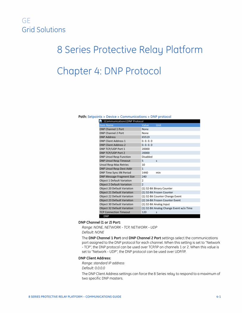
Path: Setpoints > Device > Communications > DNP protocol
DNP Channel (1 or 2) Port:Range: NONE, NETWORK - TCP, NETWORK - UDPDefault: NONE
The DNP Channel 1 Port and DNP Channel 2 Port settings select the communications port assigned to the DNP protocol for each channel. When this setting is set to “Network - TCP”, the DNP protocol can be used over TCP/IP on channels 1 or 2. When this value is set to “Network - UDP”, the DNP protocol can be used over UDP/IP.
DNP Client Address:Range: standard IP addressDefault: 0.0.0.0
The DNP Client Address settings can force the 8 Series relay to respond to a maximum of two specific DNP masters.
..\Communications\DNP ProtocolItem Name Value UnitDNP Channel 1 Port NoneDNP Channel 2 Port NoneDNP Address 65519DNP Client Address 1 0. 0. 0. 0DNP Client Address 2 0. 0. 0. 0DNP TCP/UDP Port 1 20000DNP TCP/UDP Port 2 20000DNP Unsol Resp Function DisabledDNP Unsol Resp Timeout 5 sUnsol Resp Max Retries 10DNP Unsol Resp Dest Addr 1DNP Time Sync IIN Period 1440 minDNP Message Fragment Size 240Object 1 Default Variation 2Object 2 Default Variation 2Object 20 Default Variation (1) 32-Bit Binary CounterObject 21 Default Variation (1) 32-Bit Frozen CounterObject 22 Default Variation (1) 32-Bit Counter Change EventObject 23 Default Variation (2) 16-Bit Frozen Counter EventObject 30 Default Variation (1) 32-Bit Analog InputObject 32 Default Variation (1) 32-Bit Analog Change Event w/o TimeTCP Connection Timeout 120 s
DNP
8 SERIES PROTECTIVE RELAY PLATFORM – COMMUNICATIONS GUIDE 4-1

CHAPTER 4: DNP PROTOCOL
NOTE
NOTE: “DNP Channel 1 Port” will take the “DNP TCP/UDP Port 1” and “DNP Client Address 1” to allow/reject connections. The same relation is used by channel 2.
DNP Address:Range: 0 to 65519 in steps of 1Default: 65519
The DNP address sets the DNP slave address. This number identifies the 8 Series relay on a DNP communications link. Each DNP slave must be assigned a unique address.
DNP Unsol Resp Function:Range: Enabled, DisabledDefault: Disabled
This setting will take effect for Ethernet communication only if the main card is present or a comms card is available in the device. This setting enables/disables the unsolicited response functionality. It is disabled for RS485 applications since there is no collision avoidance mechanism.
DNP Unsol Resp Timeout:Range: 0 to 60 s in steps of 1Default: 5 s
Sets the time the 8 Series relay waits for a DNP master to confirm an unsolicited response.
Unsol Resp Max Retries: Range: 1 to 255 in steps of 1Default: 10
Sets the number of times the 8 Series relay retransmits an unsolicited response without receiving confirmation from the master; a value of “255” allows infinite re-tries.
DNP Unsol Resp Dest Addr: Range: 1 to 65519 in steps of 1Default: 1
Sets the DNP address to which all unsolicited responses are sent. The IP address to which unsolicited responses are sent is determined by the 8 Series relay from the current TCP connection or the most recent UDP message.
DNP Time Sync IIN Period:Range: 1 to 10080 min. in steps of 1Default: 1440 min
This setting determines how often the Need Time Internal Indication (IIN) bit is set by the 8 Series relay. Changing this time allows the DNP master to send time synchronization commands more or less often, as required.
NOTE
NOTE: If the requirement for synchronization is more than a couple of seconds, the user is advised to consider synchronization via other means such as IRIGB or 1588. Given network asymmetry, the consistency of the network latency, clock drift, and additional delays due to routers located between the client and the 8 Series relay all contribute error.
DNP Message Fragment Size:Range: 30 to 2048 in steps of 1Default: 240
This setting determines the size, in bytes, at which message fragmentation occurs. Large fragment sizes allow for more efficient throughput; smaller fragment sizes cause more application layer confirmations to be necessary which can provide for more robust data transfer over noisy communication channels.
4-2 8 SERIES PROTECTIVE RELAY PLATFORM – COMMUNICATIONS GUIDE
CHAPTER 4: DNP PROTOCOL DNP COMMUNICATION
DNP OBJECT 1 Default Variation to DNP Object 32 Default Variation:
These settings allow the user to select the DNP default variation number for object types 1, 2, 20, 21, 22, 23, 30, and 32. The default variation refers to the variation response when variation 0 is requested and/or in class 0, 1, 2, or 3 scans.
TCP Connection Timeout:Range: 10 to 300 s in steps of 1Default: 120 s
This setting specifies a time delay for the detection of dead network TCP connections. If there is no data traffic on a DNP TCP connection for greater than the time specified by this setting, the connection will be aborted by the 8 Series relay. This frees up the connection to be re-used by a client.
DNP communication
The 8 Series relay supports Distributed Network Protocol (DNP) version 3.0. and the 8 Series relay operates as a DNP slave device. Two DNP masters can actively communicate with the 8 Series relay at one time as the 8 Series relay maintains two sets of DNP data change buffers and connection information. The following is a detailed explanation of the 8 Series relay ’s DNP 3 implementation.
FASTPATH: Both DNP and IEC104 protocol can work at the same time, but the user has to consider that there is only one point map. So, the two protocols will use the same data mapping, i.e. the same point index and same point source.
FASTPATH: The 8 Series relay supports two DNP3.0 client connections simultaneously.
FASTPATH: When configuring DNP do not use port 20057 since it is reserved for internal purposes by the unit itself.
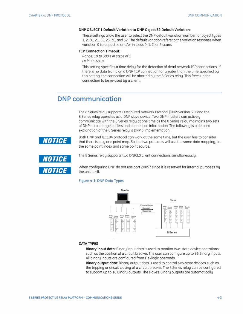
Figure 4-1: DNP Data Types
DATA TYPESBinary input data: Binary input data is used to monitor two-state device operations such as the position of a circuit breaker. The user can configure up to 96 Binary inputs. All binary inputs are configured from Flexlogic operands.Binary output data: Binary output data is used to control two-state devices such as the tripping or circuit closing of a circuit breaker. The 8 Series relay can be configured to support up to 16 Binary outputs. The slave’s Binary outputs are automatically
8 SERIES PROTECTIVE RELAY PLATFORM – COMMUNICATIONS GUIDE 4-3
DNP COMMUNICATION CHAPTER 4: DNP PROTOCOL
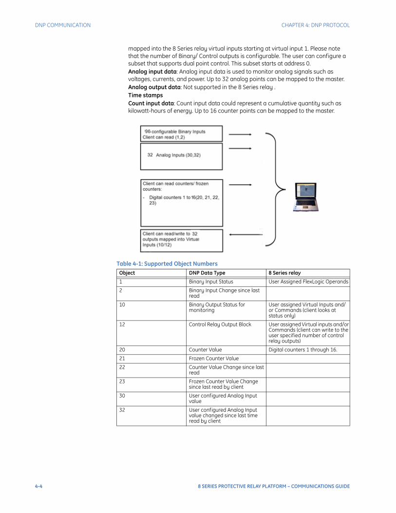
mapped into the 8 Series relay virtual inputs starting at virtual input 1. Please note that the number of Binary/ Control outputs is configurable. The user can configure a subset that supports dual point control. This subset starts at address 0. Analog input data: Analog input data is used to monitor analog signals such as voltages, currents, and power. Up to 32 analog points can be mapped to the master.Analog output data: Not supported in the 8 Series relay .Time stamps Count input data: Count input data could represent a cumulative quantity such as kilowatt-hours of energy. Up to 16 counter points can be mapped to the master.
Table 4-1: Supported Object NumbersObject DNP Data Type 8 Series relay
1 Binary Input Status User Assigned FlexLogic Operands
2 Binary Input Change since last read
10 Binary Output Status for monitoring
User assigned Virtual Inputs and/or Commands (client looks at status only)
12 Control Relay Output Block User assigned Virtual inputs and/or Commands (client can write to the user specified number of control relay outputs)
20 Counter Value Digital counters 1 through 16.
21 Frozen Counter Value
22 Counter Value Change since last read
23 Frozen Counter Value Change since last read by client
30 User configured Analog Input value
32 User configured Analog Input value changed since last time read by client
4-4 8 SERIES PROTECTIVE RELAY PLATFORM – COMMUNICATIONS GUIDE
CHAPTER 4: DNP PROTOCOL DNP COMMUNICATION
The following setpoints are in the PATH: SETPOINTS > DEVICE > COMMUNICATIONS > DNP PROTOCOL
DNP CHANNEL 1 PORTRange: NONE, NETWORK - TCP, NETWORK- UDPDefault: NONE
DNP CHANNEL 2 PORTRange: NONE, NETWORK - TCP, NETWORK- UDPDefault: NONE
The DNP Channel 1 Port and DNP Channel 2 Port settings select the communications port assigned to the DNP protocol for each channel. When this setting is set to “Network - TCP,” the DNP protocol can be used over TCP/IP on channels 1 or 2. When this value is set to “Network - UDP,” the DNP protocol can be used over UDP/IP.
FASTPATH: If the additional communication module is not present, only RS485 is a possible option. The Network options are hidden in this case and the DNP channel is assigned to the RS485 port by default.
DNP ADDRESSRange: 0 to 65519 in steps of 1Default: 65519
Sets the DNP slave address. This number identifies this 8 Series relay on a DNP communications link. Each DNP slave should be assigned a unique address.
DNP NETWORK CLIENT ADDRESS 1(2)Range: Standard IP AddressDefault: 0.0.0.0
The DNP Network Client Address settings can force the 8 Series relay to respond to a maximum of two specific DNP masters.
DNP TCP/UDP PORT NUMBER 1 (2)Range: 1 to 65535 in steps of 1Default: 20000
The DNP NETWORK CLIENT ADDRESS 1(2) and DNP TCP/UDP PORT NUMBER 1(2) settings are available only if the communications card is present. “DNP Channel 1 Port” takes the “Port Number 1” and “Client Address 1” to allow or reject connections. The same relation is used by channel 2.
DNP UNSOL RESPONSE FUNCTIONRange: Enabled, DisabledDefault: Disabled
Should be “Disabled” for RS485 applications since there is no collision avoidance mechanism. Unsolicited response settings is hidden if the communication card is not present, as DNP runs only on RS485 in this case.
Analog Variation Numbers Data Format
1 32-bit integer value with flag
2 16-bit integer value with flag
3 32-bit integer value without flag
4 16-bit integer value without flag
5 32-bit floating point value with flag
8 SERIES PROTECTIVE RELAY PLATFORM – COMMUNICATIONS GUIDE 4-5

DNP COMMUNICATION CHAPTER 4: DNP PROTOCOL
DNP UNSOL RESPONSE TIMEOUTRange: 0 to 60 s in steps of 1 sDefault: 5 s
Sets the time the 8 Series relay waits for a DNP master to confirm an unsolicited response.
DNP UNSOL RESPONSE MAX RETRIESRange: 1 to 255 in steps of 1Default: 10
Sets the number of times the 8 Series relay retransmits an unsolicited response without receiving confirmation from the master; a value of “255” allows infinite re-tries.
DNP UNSOL RESPONSE DEST ADDRESSRange: 0 to 65519 in steps of 1Default: 1
Sets the DNP address to which all unsolicited responses are sent. The IP address to which unsolicited responses are sent is determined by the 8 Series relay from the current TCP connection or the most recent UDP message.
DNP TIME SYNC IIN PERIODRange: 1 to 10080 min in steps of 1 minDefault: 1440 min
This setting determines how often the Need Time Internal Indication (IIN) bit is set by the 8 Series relay . Changing this time requires the DNP master to send time synchronization commands more or less often, as this setting time period.
FASTPATH: If the requirement for time synchronization is more than a couple of seconds the user is advised to consider time-sync via other means such as IRIG-B or 1588, given network asymmetry, the consistency of the network latency, clock drift and additional delays due to routers located between the client and the 8 Series relay , all of which contribute errors.
DNP MESSAGE FRAGMENT SIZERange: 30 to 2048 in steps of 1Default: 240
This setting determines the size (maximum length of frame), in bytes, at which message fragmentation occurs. Large fragment sizes allow for more efficient throughput; smaller fragment sizes cause more application layer confirmations to be necessary which can provide for more robust data transfer over noisy communication channels.
DNP OBJECT 1(2) DEFAULT VARIATIONRange: 1, 2Default: 2
These settings allow the user to select the DNP default variation number for object types 1, 2, 20, 21, 22, 23, 30, and 32. The default variation refers to the variation response when variation 0 is requested and/or in class 0, 1, 2, or 3 scans. The DNP binary outputs typically map one-to-one to IED data points. That is, each DNP binary output controls a single physical or virtual control point in an IED. In the 8 Series relay, DNP binary outputs are mapped to virtual inputs.
DNP OBJECT 20(22) DEFAULT VARIATIONRange: 1, 2, 5, 6Default: 1
For explanation, see above.
4-6 8 SERIES PROTECTIVE RELAY PLATFORM – COMMUNICATIONS GUIDE
CHAPTER 4: DNP PROTOCOL DNP DEVICE PROFILE
DNP OBJECT 21 DEFAULT VARIATIONRange: 1, 2, 9, 10Default: 1
For explanation, see above.
DNP OBJECT 23 DEFAULT VARIATIONRange: 1, 2, 5, 6Default: 2
For explanation, see above.
DNP OBJECT 30 DEFAULT VARIATIONRange: 1, 2, 3, 4, 5Default: 1
For explanation, see above.
DNP OBJECT 32 DEFAULT VARIATIONRange: 1, 2, 3, 4, 5, 7Default: 1
For explanation, see above.
DNP TCP CONNECTION TIMEOUTRange: 10 to 300 s in steps of 1 sDefault: 120 s
The setting specifies a time delay for the detection of failed network TCP connections. If there is no data traffic on a DNP TCP connection for greater than the time specified by the setting, the connection is aborted by the 8 Series relay. This frees up the resource for the connection and allows another DNP TCP connection request.
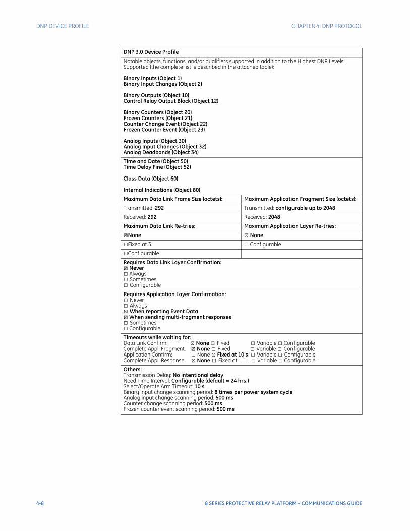
DNP device profile
DNP 3.0 Device Profile
(Also see the IMPLEMENTATION TABLE in the following section)
Vendor Name: General Electric Multilin
Device Name: 8 Series relay
Highest DNP Level Supported:For Requests: Level 2For Responses: Level 2
Device Function:□ Master⊠ Slave
8 SERIES PROTECTIVE RELAY PLATFORM – COMMUNICATIONS GUIDE 4-7
DNP DEVICE PROFILE CHAPTER 4: DNP PROTOCOL
Notable objects, functions, and/or qualifiers supported in addition to the Highest DNP Levels Supported (the complete list is described in the attached table):
Binary Inputs (Object 1)Binary Input Changes (Object 2)
Binary Outputs (Object 10)Control Relay Output Block (Object 12)
Binary Counters (Object 20)Frozen Counters (Object 21)Counter Change Event (Object 22)Frozen Counter Event (Object 23)
Analog Inputs (Object 30)Analog Input Changes (Object 32)Analog Deadbands (Object 34)
Time and Date (Object 50)Time Delay Fine (Object 52)
Class Data (Object 60)
Internal Indications (Object 80)
Maximum Data Link Frame Size (octets): Maximum Application Fragment Size (octets):
Transmitted: 292 Transmitted: configurable up to 2048
Received: 292 Received: 2048
Maximum Data Link Re-tries: Maximum Application Layer Re-tries:
⊠None ⊠ None
□Fixed at 3 □ Configurable
□Configurable
Requires Data Link Layer Confirmation:⊠ Never□ Always□ Sometimes□ Configurable
Requires Application Layer Confirmation:□ Never□ Always⊠ When reporting Event Data⊠ When sending multi-fragment responses□ Sometimes□ Configurable
Timeouts while waiting for:Data Link Confirm: ⊠ None □ Fixed □ Variable □ ConfigurableComplete Appl. Fragment: ⊠ None □ Fixed □ Variable □ ConfigurableApplication Confirm: □ None ⊠ Fixed at 10 s □ Variable □ ConfigurableComplete Appl. Response: ⊠ None □ Fixed at ___ □ Variable □ Configurable
Others:Transmission Delay: No intentional delayNeed Time Interval: Configurable (default = 24 hrs.)Select/Operate Arm Timeout: 10 sBinary input change scanning period: 8 times per power system cycleAnalog input change scanning period: 500 msCounter change scanning period: 500 msFrozen counter event scanning period: 500 ms
DNP 3.0 Device Profile
4-8 8 SERIES PROTECTIVE RELAY PLATFORM – COMMUNICATIONS GUIDE
CHAPTER 4: DNP PROTOCOL DNP DEVICE PROFILE
Sends/Executes Control Operations:WRITE Binary Outputs ⊠ Never □ Always □ Sometimes □ ConfigurableSELECT/OPERATE □ Never ⊠ Always □ Sometimes □ ConfigurableDIRECT OPERATE □ Never ⊠ Always □ Sometimes □ ConfigurableDIRECT OPERATE – NO ACK □ Never ⊠ Always □ Sometimes □ ConfigurableCount > 1 ⊠ Never □ Always □ Sometimes □ ConfigurablePulse On □ Never □ Always ⊠ Sometimes □ ConfigurablePulse Off □ Never □ Always ⊠ Sometimes □ ConfigurableLatch On □ Never □ Always ⊠ Sometimes □ ConfigurableLatch Off □ Never □ Always ⊠ Sometimes □ ConfigurableQueue ⊠ Never □ Always □ Sometimes □ ConfigurableClear Queue ⊠ Never □ Always □ Sometimes □ Configurable
Explanation of ‘Sometimes’: Object 12 points are mapped to Virtual Inputs and Commands (Force Coils). Both “Pulse On” and “Latch On” operations perform the same function in the 8 Series relay ; that is, the appropriate Virtual Input or Coil is put into the “On” state. The On/Off times and Count value are ignored. “Pulse Off” and “Latch Off” operations put the appropriate Virtual Input or Coil into the “Off” state. “Trip” and “Close” operations both put the appropriate Virtual Input or coil into the “On” state if a paired mapping is set, otherwise “Trip” will put into “Off” and “Close” will put into “On”.
Reports Binary Input Change Events when no specific variation requested:
□ Never⊠ Only time-tagged□ Only non-time-tagged□ Configurable
Reports time-tagged Binary Input Change Events when no specific variation requested:□ Never⊠ Binary Input Change With Time□ Binary Input Change With Relative Time□ Configurable (attach explanation)
Sends Unsolicited Responses:□ Never□ Configurable□ Only certain objects⊠ Sometimes⊠ ENABLE/DISABLE unsolicited Function codes supported
Sends Static Data in Unsolicited Responses:⊠ Never□ When Device Restarts□ When Status Flags ChangeNo other options are permitted.
Explanation of ‘Sometimes’: It will be disabled for RS-485 applications, since there is no collision avoidance mechanism. For Ethernet communication it will be available and it can be disabled or enabled with the proper function code.
Default Counter Object/Variation:□ No Counters Reported□ Configurable (attach explanation)⊠ Default Object: 20Default Variation: 1⊠ Point-by-point list attached
Counters Roll Over at:□ No Counters Reported□ Configurable (attach explanation)⊠ 16 Bits□ 32 Bits□ Other Value: _____⊠ Point-by-point list attached
Sends Multi-Fragment Responses:⊠ Yes□ No
DNP 3.0 Device Profile
8 SERIES PROTECTIVE RELAY PLATFORM – COMMUNICATIONS GUIDE 4-9
DNP IMPLEMENTATION CHAPTER 4: DNP PROTOCOL
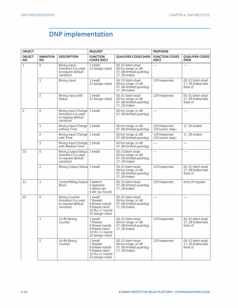
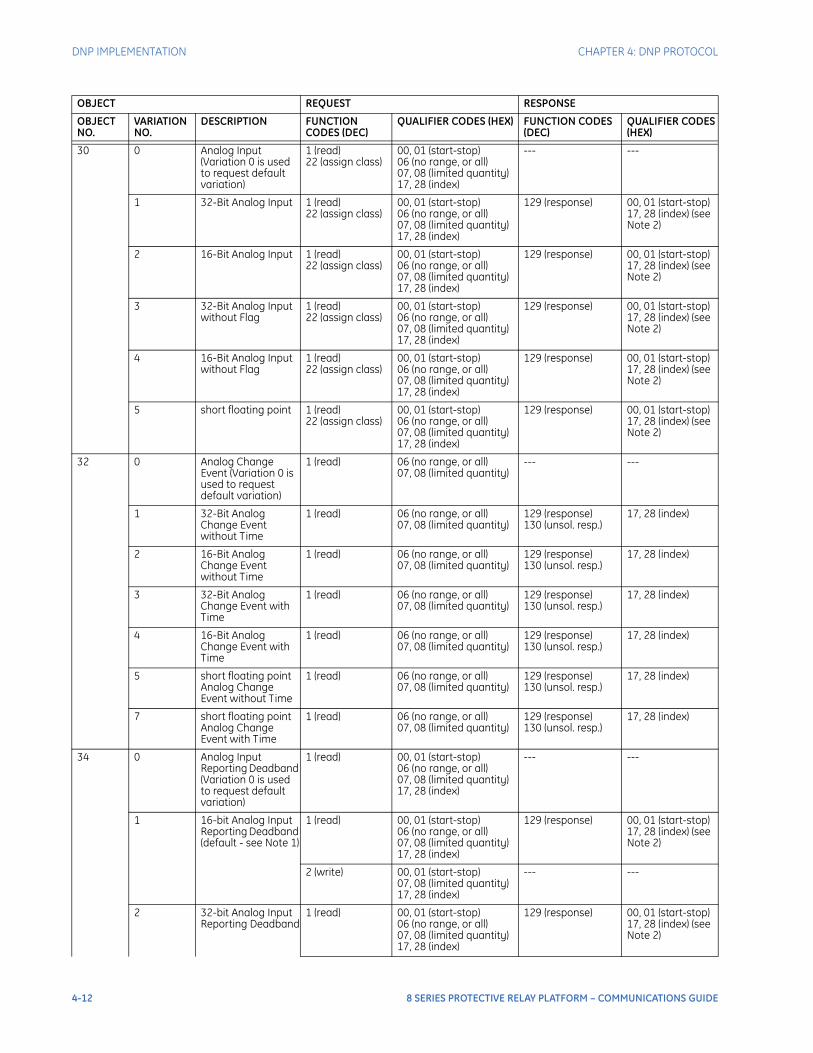
DNP implementation
OBJECT REQUEST RESPONSE
OBJECT NO.
VARIATION NO.
DESCRIPTION FUNCTION CODES (DEC)
QUALIFIER CODES (HEX) FUNCTION CODES (DEC)
QUALIFIER CODES (HEX)
1 0 Binary Input (Variation 0 is used to request default variation)
1 (read) 22 (assign class)
00, 01 (start-stop) 06 (no range, or all)07, 08 (limited quantity) 17, 28 (index)
--- ---
1 Binary Input 1 (read) 22 (assign class)
00, 01 (start-stop) 06 (no range, or all)07, 08 (limited quantity) 17, 28 (index)
129 (response) 00, 01 (start-stop) 17, 28 (index) (see Note 2)
2 Binary Input with Status
1 (read) 22 (assign class)
00, 01 (start-stop) 06 (no range, or all)07, 08 (limited quantity) 17, 28 (index)
129 (response) 00, 01 (start-stop) 17, 28 (index) (see Note 2)
2 0 Binary Input Change (Variation 0 is used to request default variation)
1 (read) 06 (no range, or all) 07, 08 (limited quantity)
--- ---
1 Binary Input Change without Time
1 (read) 06 (no range, or all) 07, 08 (limited quantity)
129 (response) 130 (unsol. resp.)
17, 28 (index)
2 Binary Input Change with Time
1 (read) 06 (no range, or all) 07, 08 (limited quantity)
129 (response) 130 (unsol. resp.)
17, 28 (index)
3 Binary Input Change with Relative Time
1 (read) 06 (no range, or all) 07, 08 (limited quantity)
--- ---
10 0 Binary Output Status (Variation 0 is used to request default variation)
1 (read) 00, 01(start-stop) 06 (no range, or all)07, 08 (limited quantity) 17, 28 (index)
--- ---
2 Binary Output Status 1 (read) 00, 01 (start-stop)06 (no range, or all)07, 08 (limited quantity)17, 28 (index)
129 (response) 00, 01 (start-stop) 17, 28 (index) (see Note 2)
12 1 Control Relay Output Block
3 (select)4 (operate) 5 (direct op) 6 (dir. op, noack)
00, 01 (start-stop)07, 08 (limited quantity)17, 28 (index)
129 (response) echo of request
20 0 Binary Counter (Variation 0 is used to request default variation)
1 (read) 7 (freeze) 8 (freeze noack) 9 (freeze clear) 10 (frz. cl. noack) 22 (assign class)
00, 01 (start-stop) 06 (no range, or all) 07, 08 (limited quantity) 17, 28 (index)
--- ---
1 32-Bit Binary Counter
1 (read)7 (freeze) 8 (freeze noack) 9 (freeze clear) 10 (frz. cl. noack) 22 (assign class)
00, 01 (start-stop) 06 (no range, or all) 07, 08 (limited quantity) 17, 28 (index)
129 (response) 00, 01 (start-stop) 17, 28 (index) (see Note 2)
2 16-Bit Binary Counter
1 (read) 7 (freeze) 8 (freeze noack) 9 (freeze clear) 10 (frz. cl. noack) 22 (assign class)
00, 01 (start-stop) 06 (no range, or all) 07, 08 (limited quantity) 17, 28 (index)
129 (response) 00, 01 (start-stop) 17, 28 (index) (see Note 2)
4-10 8 SERIES PROTECTIVE RELAY PLATFORM – COMMUNICATIONS GUIDE
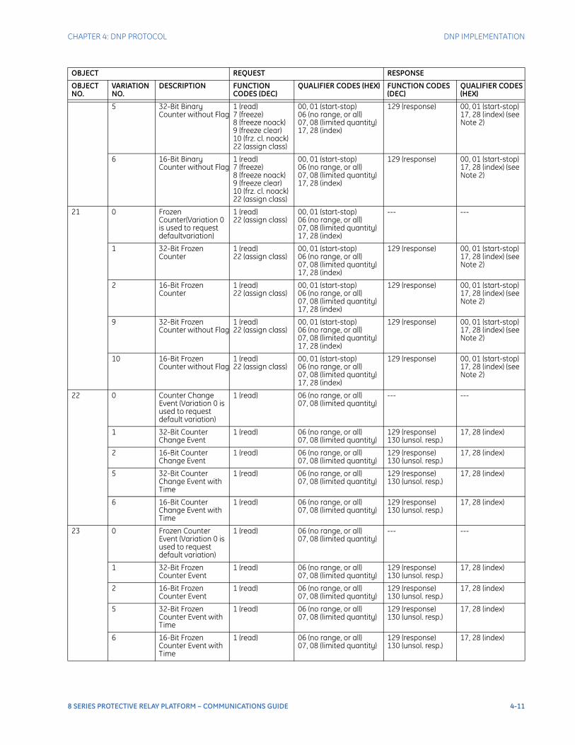
CHAPTER 4: DNP PROTOCOL DNP IMPLEMENTATION
5 32-Bit Binary Counter without Flag
1 (read) 7 (freeze) 8 (freeze noack) 9 (freeze clear) 10 (frz. cl. noack) 22 (assign class)
00, 01 (start-stop) 06 (no range, or all) 07, 08 (limited quantity) 17, 28 (index)
129 (response) 00, 01 (start-stop) 17, 28 (index) (see Note 2)
6 16-Bit Binary Counter without Flag
1 (read) 7 (freeze) 8 (freeze noack) 9 (freeze clear) 10 (frz. cl. noack) 22 (assign class)
00, 01 (start-stop) 06 (no range, or all) 07, 08 (limited quantity) 17, 28 (index)
129 (response) 00, 01 (start-stop) 17, 28 (index) (see Note 2)
21 0 Frozen Counter(Variation 0 is used to request defaultvariation)
1 (read) 22 (assign class)
00, 01 (start-stop) 06 (no range, or all) 07, 08 (limited quantity) 17, 28 (index)
--- ---
1 32-Bit Frozen Counter
1 (read) 22 (assign class)
00, 01 (start-stop) 06 (no range, or all) 07, 08 (limited quantity) 17, 28 (index)
129 (response) 00, 01 (start-stop) 17, 28 (index) (see Note 2)
2 16-Bit Frozen Counter
1 (read) 22 (assign class)
00, 01 (start-stop) 06 (no range, or all) 07, 08 (limited quantity) 17, 28 (index)
129 (response) 00, 01 (start-stop) 17, 28 (index) (see Note 2)
9 32-Bit Frozen Counter without Flag
1 (read) 22 (assign class)
00, 01 (start-stop) 06 (no range, or all) 07, 08 (limited quantity) 17, 28 (index)
129 (response) 00, 01 (start-stop) 17, 28 (index) (see Note 2)
10 16-Bit Frozen Counter without Flag
1 (read) 22 (assign class)
00, 01 (start-stop) 06 (no range, or all) 07, 08 (limited quantity) 17, 28 (index)
129 (response) 00, 01 (start-stop) 17, 28 (index) (see Note 2)
22 0 Counter Change Event (Variation 0 is used to request default variation)
1 (read) 06 (no range, or all) 07, 08 (limited quantity)
--- ---
1 32-Bit Counter Change Event
1 (read) 06 (no range, or all) 07, 08 (limited quantity)
129 (response) 130 (unsol. resp.)
17, 28 (index)
2 16-Bit Counter Change Event
1 (read) 06 (no range, or all) 07, 08 (limited quantity)
129 (response) 130 (unsol. resp.)
17, 28 (index)
5 32-Bit Counter Change Event with Time
1 (read) 06 (no range, or all) 07, 08 (limited quantity)
129 (response) 130 (unsol. resp.)
17, 28 (index)
6 16-Bit Counter Change Event with Time
1 (read) 06 (no range, or all) 07, 08 (limited quantity)
129 (response) 130 (unsol. resp.)
17, 28 (index)
23 0 Frozen Counter Event (Variation 0 is used to request default variation)
1 (read) 06 (no range, or all) 07, 08 (limited quantity)
--- ---
1 32-Bit Frozen Counter Event
1 (read) 06 (no range, or all) 07, 08 (limited quantity)
129 (response) 130 (unsol. resp.)
17, 28 (index)
2 16-Bit Frozen Counter Event
1 (read) 06 (no range, or all) 07, 08 (limited quantity)
129 (response) 130 (unsol. resp.)
17, 28 (index)
5 32-Bit Frozen Counter Event with Time
1 (read) 06 (no range, or all) 07, 08 (limited quantity)
129 (response) 130 (unsol. resp.)
17, 28 (index)
6 16-Bit Frozen Counter Event with Time
1 (read) 06 (no range, or all) 07, 08 (limited quantity)
129 (response) 130 (unsol. resp.)
17, 28 (index)
OBJECT REQUEST RESPONSE
OBJECT NO.
VARIATION NO.
DESCRIPTION FUNCTION CODES (DEC)
QUALIFIER CODES (HEX) FUNCTION CODES (DEC)
QUALIFIER CODES (HEX)
8 SERIES PROTECTIVE RELAY PLATFORM – COMMUNICATIONS GUIDE 4-11
DNP IMPLEMENTATION CHAPTER 4: DNP PROTOCOL
30 0 Analog Input (Variation 0 is used to request default variation)
1 (read) 22 (assign class)
00, 01 (start-stop) 06 (no range, or all) 07, 08 (limited quantity) 17, 28 (index)
--- ---
1 32-Bit Analog Input 1 (read) 22 (assign class)
00, 01 (start-stop) 06 (no range, or all) 07, 08 (limited quantity) 17, 28 (index)
129 (response) 00, 01 (start-stop) 17, 28 (index) (see Note 2)
2 16-Bit Analog Input 1 (read) 22 (assign class)
00, 01 (start-stop) 06 (no range, or all) 07, 08 (limited quantity) 17, 28 (index)
129 (response) 00, 01 (start-stop) 17, 28 (index) (see Note 2)
3 32-Bit Analog Input without Flag
1 (read) 22 (assign class)
00, 01 (start-stop) 06 (no range, or all) 07, 08 (limited quantity) 17, 28 (index)
129 (response) 00, 01 (start-stop) 17, 28 (index) (see Note 2)
4 16-Bit Analog Input without Flag
1 (read) 22 (assign class)
00, 01 (start-stop) 06 (no range, or all) 07, 08 (limited quantity) 17, 28 (index)
129 (response) 00, 01 (start-stop) 17, 28 (index) (see Note 2)
5 short floating point 1 (read) 22 (assign class)
00, 01 (start-stop) 06 (no range, or all) 07, 08 (limited quantity) 17, 28 (index)
129 (response) 00, 01 (start-stop) 17, 28 (index) (see Note 2)
32 0 Analog Change Event (Variation 0 is used to request default variation)
1 (read) 06 (no range, or all) 07, 08 (limited quantity)
--- ---
1 32-Bit Analog Change Event without Time
1 (read) 06 (no range, or all) 07, 08 (limited quantity)
129 (response) 130 (unsol. resp.)
17, 28 (index)
2 16-Bit Analog Change Event without Time
1 (read) 06 (no range, or all) 07, 08 (limited quantity)
129 (response) 130 (unsol. resp.)
17, 28 (index)
3 32-Bit Analog Change Event with Time
1 (read) 06 (no range, or all) 07, 08 (limited quantity)
129 (response) 130 (unsol. resp.)
17, 28 (index)
4 16-Bit Analog Change Event with Time
1 (read) 06 (no range, or all) 07, 08 (limited quantity)
129 (response) 130 (unsol. resp.)
17, 28 (index)
5 short floating point Analog Change Event without Time
1 (read) 06 (no range, or all) 07, 08 (limited quantity)
129 (response) 130 (unsol. resp.)
17, 28 (index)
7 short floating point Analog Change Event with Time
1 (read) 06 (no range, or all) 07, 08 (limited quantity)
129 (response) 130 (unsol. resp.)
17, 28 (index)
34 0 Analog Input Reporting Deadband (Variation 0 is used to request default variation)
1 (read) 00, 01 (start-stop) 06 (no range, or all) 07, 08 (limited quantity) 17, 28 (index)
--- ---
1 16-bit Analog Input Reporting Deadband (default - see Note 1)
1 (read) 00, 01 (start-stop) 06 (no range, or all) 07, 08 (limited quantity) 17, 28 (index)
129 (response) 00, 01 (start-stop) 17, 28 (index) (see Note 2)
2 (write) 00, 01 (start-stop) 07, 08 (limited quantity) 17, 28 (index)
--- ---
2 32-bit Analog Input Reporting Deadband
1 (read) 00, 01 (start-stop) 06 (no range, or all) 07, 08 (limited quantity) 17, 28 (index)
129 (response) 00, 01 (start-stop) 17, 28 (index) (see Note 2)
OBJECT REQUEST RESPONSE
OBJECT NO.
VARIATION NO.
DESCRIPTION FUNCTION CODES (DEC)
QUALIFIER CODES (HEX) FUNCTION CODES (DEC)
QUALIFIER CODES (HEX)
4-12 8 SERIES PROTECTIVE RELAY PLATFORM – COMMUNICATIONS GUIDE

CHAPTER 4: DNP PROTOCOL DNP IMPLEMENTATION
FASTPATH: 1. A default variation refers to the variation response when variation 0 is requested and/or in class 0, 1, 2, or 3 scans. The default variations for object types 1, 2, 20, 21, 22, 23, 30, and 32 are selected via relay settings. This optimizes the class 0 poll data size.
2. For static (non-change-event) objects, qualifiers 17 or 28 are only responded when a request is sent with qualifiers 17 or 28, respectively. Otherwise, static object requests sent with qualifiers 00, 01, 06, 07, or 08, will be responded with qualifiers 00 or 01 (for changeevent objects, qualifiers 17 or 28 are always responded.)
Cold restarts are implemented the same as warm restarts – the 8 Series relay is not restarted, but the DNP process is restarted.
2 (write) 00, 01 (start-stop) 07, 08 (limited quantity) 17, 28 (index)
--- ---
50 1 Time and Date (default - see Note 1)
1 (read)2 (write)
00, 01 (start-stop) 06 (no range, or all) 07 (limited qty=1) 08 (limited quantity) 17, 28 (index)
129 (response) 00, 01 (start-stop) 17, 28 (index) (see Note 2)
52 2 Time Delay Fine (quantity = 1)
129 (response) 07 (limited quantity) --- ---
60 0 Class 0, 1, 2, and 3 Data
1 (read) 20 (enable unsol) 21 (disable unsol) 22 (assign class)
06 (no range, or all) --- ---
1 Class 0 Data 1 (read) 22 (assign class)
06 (no range, or all) --- ---
2 Class 1 Data 1 (read) 20 (enable unsol)
06 (no range, or all) 07, 08 (limited quantity)
--- ---
3 Class 2 Data 21 (disable unsol) --- ---
4 Class 3 Data 22 (assign class) --- ---
80 1 Internal Indications 1 (read) 00, 01 (start-stop) (index =7)
129 (response) 00, 01 (start-stop)
2 (write) (see Note 3)
00 (start-stop) (index =7)
--- ---
No Object (function code only) see Note 3
13 (cold restart) --- --- ---
No Object (function code only)
14 (warm restart) --- --- ---
No Object (function code only)
23 (delay meas.) --- --- ---
OBJECT REQUEST RESPONSE
OBJECT NO.
VARIATION NO.
DESCRIPTION FUNCTION CODES (DEC)
QUALIFIER CODES (HEX) FUNCTION CODES (DEC)
QUALIFIER CODES (HEX)
8 SERIES PROTECTIVE RELAY PLATFORM – COMMUNICATIONS GUIDE 4-13

DNP IMPLEMENTATION CHAPTER 4: DNP PROTOCOL
4-14 8 SERIES PROTECTIVE RELAY PLATFORM – COMMUNICATIONS GUIDE

8 Series Protective Relay Platform
Chapter 5: DNP / IEC104 Point Lists
GEGrid Solutions
DNP / IEC104 Point Lists
The menu for the DNP/IEC104 point lists is shown below.Path: Setpoints > Device > Communications > DNP/IEC104 Point Lists
The binary inputs points for the DNP protocol, or the MSP points for IEC 60870-5-104 protocol, can be configured to a maximum of 96 points. The data source for each point is user-programmable and can be configured by assigning FlexLogic operands.The menu for the binary input points (DNP) or MSP points (IEC 60870-5-104) is shown below.
8 SERIES PROTECTIVE RELAY PLATFORM – COMMUNICATIONS GUIDE 5-1
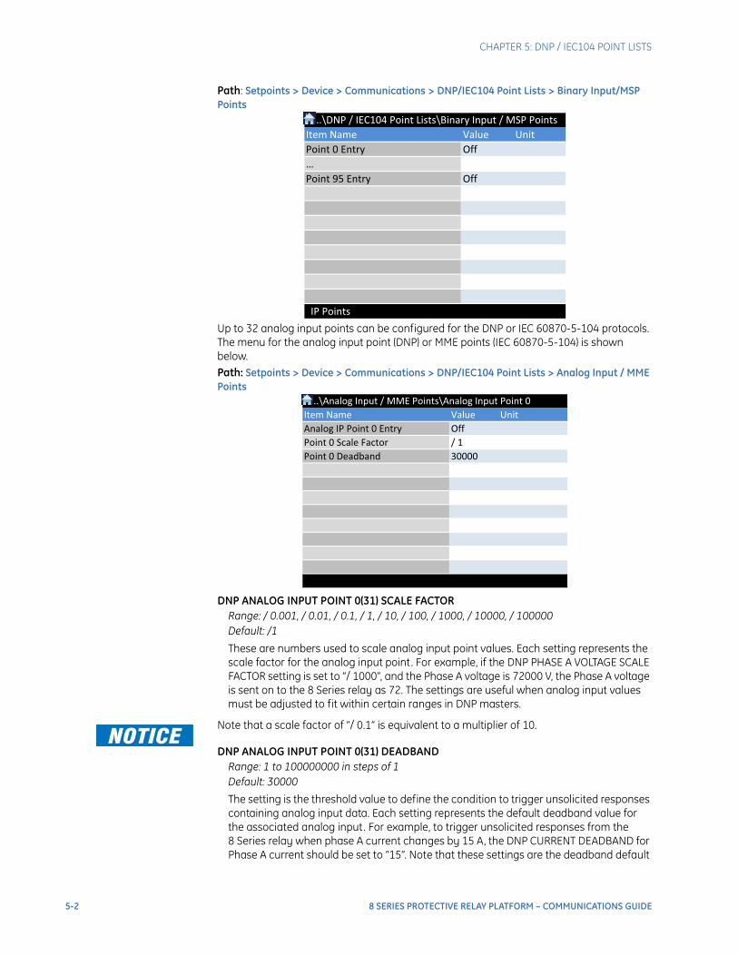
CHAPTER 5: DNP / IEC104 POINT LISTS
Path: Setpoints > Device > Communications > DNP/IEC104 Point Lists > Binary Input/MSP Points
Up to 32 analog input points can be configured for the DNP or IEC 60870-5-104 protocols. The menu for the analog input point (DNP) or MME points (IEC 60870-5-104) is shown below.Path: Setpoints > Device > Communications > DNP/IEC104 Point Lists > Analog Input / MME Points
DNP ANALOG INPUT POINT 0(31) SCALE FACTORRange: / 0.001, / 0.01, / 0.1, / 1, / 10, / 100, / 1000, / 10000, / 100000Default: /1
These are numbers used to scale analog input point values. Each setting represents the scale factor for the analog input point. For example, if the DNP PHASE A VOLTAGE SCALE FACTOR setting is set to “/ 1000”, and the Phase A voltage is 72000 V, the Phase A voltage is sent on to the 8 Series relay as 72. The settings are useful when analog input values must be adjusted to fit within certain ranges in DNP masters.
FASTPATH: Note that a scale factor of ”/ 0.1” is equivalent to a multiplier of 10.
DNP ANALOG INPUT POINT 0(31) DEADBANDRange: 1 to 100000000 in steps of 1Default: 30000
The setting is the threshold value to define the condition to trigger unsolicited responses containing analog input data. Each setting represents the default deadband value for the associated analog input. For example, to trigger unsolicited responses from the 8 Series relay when phase A current changes by 15 A, the DNP CURRENT DEADBAND for Phase A current should be set to “15”. Note that these settings are the deadband default
..\DNP / IEC104 Point Lists\Binary Input / MSP PointsItem Name Value UnitPoint 0 Entry Off�Point 95 Entry Off
IP Points
..\Analog Input / MME Points\Analog Input Point 0Item Name Value UnitAnalog IP Point 0 Entry OffPoint 0 Scale Factor / 1Point 0 Deadband 30000
5-2 8 SERIES PROTECTIVE RELAY PLATFORM – COMMUNICATIONS GUIDE
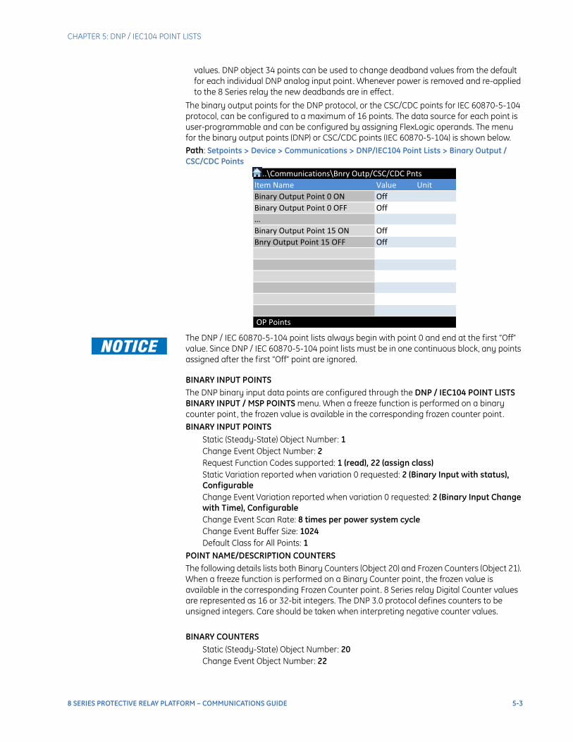
CHAPTER 5: DNP / IEC104 POINT LISTS
values. DNP object 34 points can be used to change deadband values from the default for each individual DNP analog input point. Whenever power is removed and re-applied to the 8 Series relay the new deadbands are in effect.
The binary output points for the DNP protocol, or the CSC/CDC points for IEC 60870-5-104 protocol, can be configured to a maximum of 16 points. The data source for each point is user-programmable and can be configured by assigning FlexLogic operands. The menu for the binary output points (DNP) or CSC/CDC points (IEC 60870-5-104) is shown below.Path: Setpoints > Device > Communications > DNP/IEC104 Point Lists > Binary Output / CSC/CDC Points
FASTPATH: The DNP / IEC 60870-5-104 point lists always begin with point 0 and end at the first “Off” value. Since DNP / IEC 60870-5-104 point lists must be in one continuous block, any points assigned after the first “Off” point are ignored.
BINARY INPUT POINTSThe DNP binary input data points are configured through the DNP / IEC104 POINT LISTS BINARY INPUT / MSP POINTS menu. When a freeze function is performed on a binary counter point, the frozen value is available in the corresponding frozen counter point.BINARY INPUT POINTS
Static (Steady-State) Object Number: 1Change Event Object Number: 2Request Function Codes supported: 1 (read), 22 (assign class)Static Variation reported when variation 0 requested: 2 (Binary Input with status), ConfigurableChange Event Variation reported when variation 0 requested: 2 (Binary Input Change with Time), ConfigurableChange Event Scan Rate: 8 times per power system cycleChange Event Buffer Size: 1024Default Class for All Points: 1
POINT NAME/DESCRIPTION COUNTERSThe following details lists both Binary Counters (Object 20) and Frozen Counters (Object 21). When a freeze function is performed on a Binary Counter point, the frozen value is available in the corresponding Frozen Counter point. 8 Series relay Digital Counter values are represented as 16 or 32-bit integers. The DNP 3.0 protocol defines counters to be unsigned integers. Care should be taken when interpreting negative counter values.
BINARY COUNTERSStatic (Steady-State) Object Number: 20Change Event Object Number: 22
..\Communications\Bnry Outp/CSC/CDC PntsItem Name Value UnitBinary Output Point 0 ON OffBinary Output Point 0 OFF Off�Binary Output Point 15 ON OffBnry Output Point 15 OFF Off
OP Points
8 SERIES PROTECTIVE RELAY PLATFORM – COMMUNICATIONS GUIDE 5-3
CHAPTER 5: DNP / IEC104 POINT LISTS
Request Function Codes supported: 1 (read), 7 (freeze), 8 (freeze noack), 9 (freeze and clear), 10 (freeze and clear, noack), 22 (assign class)Static Variation reported when variation 0 requested: 1 (32-Bit Binary Counter with Flag)Change Event Variation reported when variation 0 requested: 1 (32-Bit Counter Change Event without time)Change Event Buffer Size: 10Default Class for all points: 3
FROZEN COUNTERSStatic (Steady-State) Object Number: 21Change Event Object Number: 23Request Function Codes supported: 1 (read)Static Variation reported when variation 0 requested: 1 (32-Bit Frozen Counter with Flag)Change Event Variation reported when variation 0 requested: 1 (32-Bit Counter Change Event without time)Change Event Buffer Size: 10Default Class for all points: 3
BINARY AND FROZEN COUNTERS POINT INDEX NAME/DESCRIPTION0 Digital Counter 11 Digital Counter 22 Digital Counter 33 Digital Counter 44 Digital Counter 55 Digital Counter 66 Digital Counter 77 Digital Counter 88 Digital Counter 99 Digital Counter 1010 Digital Counter 1111 Digital Counter 1212 Digital Counter 1313 Digital Counter 1414 Digital Counter 1515 Digital Counter 16
ANALOG INPUTSIt is important to note that 16-bit and 32-bit variations of analog inputs are transmitted through DNP as signed numbers. Even for analog input points that are not valid as negative values, the maximum positive representation is 32767 for 16-bit values and 2147483647 for 32-bit values. This is a DNP requirement. The deadbands for all Analog Input points are in the same units as the Analog Input quantity. For example, an Analog Input quantity measured in volts has a corresponding deadband in units of volts. Relay settings are available to set default deadband values according to data type. Deadbands for individual Analog Input Points can be set using DNP Object 34.
FASTPATH: 1. A default variation refers to the variation response when variation 0 is requested and/or in class 0, 1, 2, or 3 scans. The default variations for object types 1, 2, 20, 21, 22, 23, 30, and 32 are selected via relay settings. This optimizes the class 0 poll data size.
5-4 8 SERIES PROTECTIVE RELAY PLATFORM – COMMUNICATIONS GUIDE

CHAPTER 5: DNP / IEC104 POINT LISTS
2. For static (non-change-event) objects, qualifiers 17 or 28 are only responded when a request is sent with qualifiers 17 or 28, respectively. Otherwise, static object requests sent with qualifiers 00, 01, 06, 07, or 08, are responded with qualifiers 00 or 01. For change event objects, qualifiers 17 or 28 are always responded.
Cold restarts are implemented the same as warm restarts – the 8 Series relay is not restarted, but the DNP process is restarted.
8 SERIES PROTECTIVE RELAY PLATFORM – COMMUNICATIONS GUIDE 5-5

CHAPTER 5: DNP / IEC104 POINT LISTS
5-6 8 SERIES PROTECTIVE RELAY PLATFORM – COMMUNICATIONS GUIDE
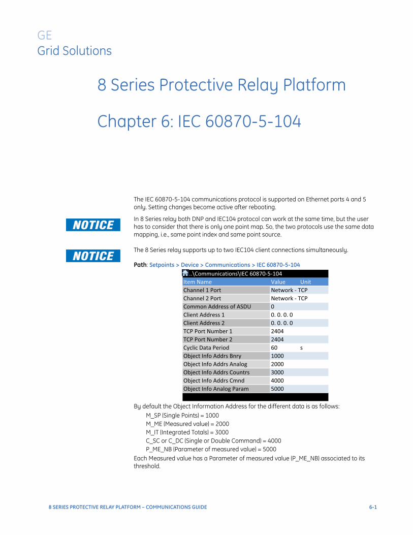
8 Series Protective Relay Platform
Chapter 6: IEC 60870-5-104
GEGrid Solutions
IEC 60870-5-104
The IEC 60870-5-104 communications protocol is supported on Ethernet ports 4 and 5 only. Setting changes become active after rebooting.
FASTPATH: In 8 Series relay both DNP and IEC104 protocol can work at the same time, but the user has to consider that there is only one point map. So, the two protocols use the same data mapping, i.e., same point index and same point source.
FASTPATH: The 8 Series relay supports up to two IEC104 client connections simultaneously.
Path: Setpoints > Device > Communications > IEC 60870-5-104
By default the Object Information Address for the different data is as follows:M_SP (Single Points) = 1000M_ME (Measured value) = 2000M_IT (Integrated Totals) = 3000C_SC or C_DC (Single or Double Command) = 4000P_ME_NB (Parameter of measured value) = 5000
Each Measured value has a Parameter of measured value (P_ME_NB) associated to its threshold.
..\Communications\IEC 60870-5-104Item Name Value UnitChannel 1 Port Network - TCPChannel 2 Port Network - TCPCommon Address of ASDU 0Client Address 1 0. 0. 0. 0Client Address 2 0. 0. 0. 0TCP Port Number 1 2404TCP Port Number 2 2404Cyclic Data Period 60 sObject Info Addrs Bnry 1000Object Info Addrs Analog 2000Object Info Addrs Countrs 3000Object Info Addrs Cmnd 4000Object Info Analog Param 5000
8 SERIES PROTECTIVE RELAY PLATFORM – COMMUNICATIONS GUIDE 6-1
INTEROPERABILITY CHAPTER 6: IEC 60870-5-104
The IEC 60870-5-104 Deadbands settings are used to determine when to trigger spontaneous responses containing M_ME_NB_1 analog data. Each setting represents the threshold value for each M_ME_NB_1 analog point.For example, to trigger spontaneous responses from the 8 Series relay when a current value changes by 15 A, the “Analog Point xx Deadband” setting should be set to 15. Note that these settings are the default values of the deadbands. P_ME_NB_1 (parameter of measured value, scaled value) points can be used to change threshold values, from the default, for each individual M_ME_NB_1 analog point. There are three ways to send the measurands to the Master station. The measurands are part of the General Group and Group 2, so when a general interrogation or group 2 interrogation takes place all the measurands are included in the response. Also, there is a cyclic data period setting where it is configured in the scan period to send the measurands to the Master. And the last way, is by sending spontaneously when a deadband overflow takes place. The IEC104 Channels sub-menu is shown below.Commands are executed over the Binary Outputs. The first 8 Binary Outputs are configured to receive Select/Operate Commands and the next 8 Binary Outputs are configured to receive Direct Execute Commands.The IEC104 CHANNEL 1 PORT and IEC104 CHANNEL 2 PORT settings select the communications port assigned to the IEC104 protocol for each channel. When this setting is set to “Network - TCP”, the IEC104 protocol can be used over TCP/IP on channels 1 or 2. The IEC104 NETWORK CLIENT ADDRESS settings can force the 8 Series relay to respond to a maximum of two specific IEC104 masters which own the configured IP Addresses. The settings in this sub-menu are shown below.
FASTPATH: “IEC104 Channel 1 Port” takes the “Port Number 1” and “Client Address 1” to allow or reject connections. The same method is used by channel 2.
GROUPS OF DATAThe data is organized into groups in order to provide values when the controlling station requests them by a general or group interrogation.
Group 1 is set by the 96 Single Points (M_SP).Group 2 is set by the 32 Measured values (M_ME).Group 3 is set by the 32 Measured thresholds (P_ME).
These 96 Single Points and 32 Measured Values are also sent as a response to a General Interrogation.The Integrated Totals (M_IT) has its own Counter Group 1, and it is sent as a response to a General Request Counter.
Interoperability
This document is adapted from the IEC 60870-5-104 standard. For this section the boxes indicate the following: ⊠ – used in the standard direction; □– not used.IEC 60870-5-104 Interoperability DocumentSystem or device:□ System definition.□ Controlling station definition (master).⊠ Controlled station definition (slave).Application layer:Transmission mode for application data:Mode 1 (least significant octet first), as defined in Clause 4.10 of IEC 60870-5-4, is used exclusively in this companion standard.Common address of ASDU:
6-2 8 SERIES PROTECTIVE RELAY PLATFORM – COMMUNICATIONS GUIDE
CHAPTER 6: IEC 60870-5-104 INTEROPERABILITY
⊠ Two octets.Information object address:⊠ Three octets. ⊠ Structured ⊠ UnstructuredCause of transmission: ⊠ Two octets (with originator address). Originator address is set to zero if not used.Maximum length of APDU.253 in both directions (the maximum length is a fixed system parameter).Selection of standard ASDUs.For the following lists, the boxes indicate the following:⊠ – used in standard direction; □ – not used.Process information in monitor direction:
Table 6-1: Process information in monitor direction
Table 6-2: Process information in control direction
Number / description Mnemonic
⊠ <1> := Single-point information M_SP_NA_1
□ <3> := Double-point information M_DP_NA_1
□ <5> := Step position information M_ST_NA_1
□ <7> := Bitstring of 32 bits M_BO_NA_1
□ <9> := Measured value, normalized value M_ME_NA_1
⊠ <11> := Measured value, scaled value M_ME_NB_1
□ <13> := Measured value, short floating point value M_ME_NC_1
⊠ <15> := Integrated totals M_IT_NA_1
□ <20> := Packed single-point information with status change detection M_SP_NA_1
□ <21> := Measured value, normalized value without quantity descriptor M_ME_ND_1
⊠ <30> := Single-point information with time tag CP56Time2a M_SP_TB_1
□ <31> := Double-point information with time tag CP56Time2a M_DP_TB_1
□ <32> := Step position information with time tag CP56Time2a M_ST_TB_1
□ <33> := Bitstring of 32 bits with time tag CP56Time2a M_BO_TB_1
□ <34> := Measured value, normalized value with time tag CP56Time2a M_ME_TD_1
⊠ <35> := Measured value, scaled value with time tag CP56Time2a M_ME_TE_1
□ <36> := Measured value, short floating point value with time tag CP56Time2a M_ME_TF_1
⊠ <37> := Integrated totals with time tag CP56Time2a M_IT_TB_1
□ <38> := Event of protection equipment with time tag CP56Time2a M_EP_TD_1
□ <39> := Packed start events of protection equipment with time tag CP56Time2a
M_EP_TE_1
□ <40> := Packed output circuit information of protection equipment with time tag CP56Time2a
M_EP_TF_1
Number / description Mnemonic
⊠ <45> := Single command C_SC_NA_1
⊠ <46> := Double command C_DC_NA_1
□ <47> := Regulating step command C_RC_NA_1
□ <48> := Set point command, normalized value C_SE_NA_1
□ <49> := Set point command, scaled value C_SE_NB_1
□ <50> := Set point command, short floating point value C_SE_NC_1
□ <51> := Bitstring of 32 bits C_BO_NA_1
⊠ <58> := Single command with time tag CP56Time2a C_SC_TA_1
⊠ <59> := Double command with time tag CP56Time2a C_DC_TA_1
□ <60> := Regulating step command with time tag CP56Time2a C_RC_TA_1
8 SERIES PROTECTIVE RELAY PLATFORM – COMMUNICATIONS GUIDE 6-3
INTEROPERABILITY CHAPTER 6: IEC 60870-5-104
Either the ASDUs of the set <45> to <51> or of the set <58> to <64> are used.
Table 6-3: System information in monitor direction
Table 6-4: System information in control direction
Table 6-5: Parameter in control direction
Table 6-6: File transfer
Type identifier and cause of transmission assignments (station-specific parameters) are shown in the following tables. In these tables, shaded boxes (░) are not required, black boxes (█) are not permitted in the companion standard, empty cells indicate the functions or ASDU are not used, and a cross (╳) indicates availability only in the standard direction.
Table 6-7: Cause of transmission numbers
□ <61> := Set point command, normalized value with time tag CP56Time2a C_SE_TA_1
□ <62> := Set point command, scaled value with time tag CP56Time2a C_SE_TB_1
□ <63> := Set point command, short floating point value with time tag CP56Time2a
C_SE_TC_1
□ <64> := Bitstring of 32 bits with time tag CP56Time2a C_BO_TA_1
Number / description Mnemonic
⊠ <70> := End of initialization M_EI_NA_1
Number / description Mnemonic
⊠ <100> := Interrogation command C_IC_NA_1
⊠ <101> := Counter interrogation command C_CI_NA_1
⊠ <102> := Read command C_RD_NA_1
⊠ <103> := Clock synchronization command (see Clause 7.6 in standard) C_CS_NA_1
⊠ <105> := Reset process command C_RP_NA_1
⊠ <107> := Test command with time tag CP56Time2a C_TS_TA_1
Number / description Mnemonic
□ <110> := Parameter of measured value, normalized value PE_ME_NA_1
⊠ <111> := Parameter of measured value, scaled value PE_ME_NB_1
□ <112> := Parameter of measured value, short floating point value PE_ME_NC_1
□ <113> := Parameter activation PE_AC_NA_1
Number / description Mnemonic
□ <120> := File ready F_FR_NA_1
□ <121> := Section ready F_SR_NA_1
□ <122> := Call directory, select file, call file, call section F_SC_NA_1
□ <123> := Last section, last segment F_LS_NA_1
□ <124> := Ack file, ack section F_AF_NA_1
□ <125> := Segment F_SG_NA_1
□ <126> := Directory (blank or X, available only in monitor [standard] direction) F_DR_TA_1
□ <127> := Query log - Request archive file F_SC_NB_1
Number Cause of transmission
1 Periodic, cyclic
2 Background scan
3 Spontaneous
4 Initialized
5 Request or requested
Number / description Mnemonic
6-4 8 SERIES PROTECTIVE RELAY PLATFORM – COMMUNICATIONS GUIDE
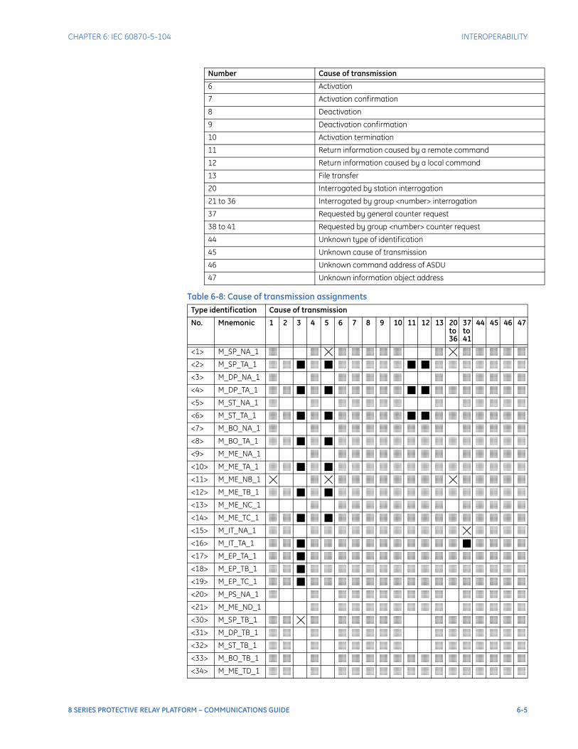
CHAPTER 6: IEC 60870-5-104 INTEROPERABILITY
Table 6-8: Cause of transmission assignments
6 Activation
7 Activation confirmation
8 Deactivation
9 Deactivation confirmation
10 Activation termination
11 Return information caused by a remote command
12 Return information caused by a local command
13 File transfer
20 Interrogated by station interrogation
21 to 36 Interrogated by group <number> interrogation
37 Requested by general counter request
38 to 41 Requested by group <number> counter request
44 Unknown type of identification
45 Unknown cause of transmission
46 Unknown command address of ASDU
47 Unknown information object address
Type identification Cause of transmission
No. Mnemonic 1 2 3 4 5 6 7 8 9 10 11 12 13 20 to 36
37 to 41
44 45 46 47
<1> M_SP_NA_1 ░ ░ ╳ ░ ░ ░ ░ ░ ░ ╳ ░ ░ ░ ░ ░<2> M_SP_TA_1 ░ ░ █ ░ █ ░ ░ ░ ░ ░ █ █ ░ ░ ░ ░ ░ ░ ░<3> M_DP_NA_1 ░ ░ ░ ░ ░ ░ ░ ░ ░ ░ ░ ░ ░<4> M_DP_TA_1 ░ ░ █ ░ █ ░ ░ ░ ░ ░ █ █ ░ ░ ░ ░ ░ ░ ░<5> M_ST_NA_1 ░ ░ ░ ░ ░ ░ ░ ░ ░ ░ ░ ░ ░<6> M_ST_TA_1 ░ ░ █ ░ █ ░ ░ ░ ░ ░ █ █ ░ ░ ░ ░ ░ ░ ░<7> M_BO_NA_1 ░ ░ ░ ░ ░ ░ ░ ░ ░ ░ ░ ░ ░ ░ ░<8> M_BO_TA_1 ░ ░ █ ░ █ ░ ░ ░ ░ ░ ░ ░ ░ ░ ░ ░ ░ ░ ░<9> M_ME_NA_1 ░ ░ ░ ░ ░ ░ ░ ░ ░ ░ ░ ░ ░ ░<10> M_ME_TA_1 ░ ░ █ ░ █ ░ ░ ░ ░ ░ ░ ░ ░ ░ ░ ░ ░ ░ ░<11> M_ME_NB_1 ╳ ░ ╳ ░ ░ ░ ░ ░ ░ ░ ░ ╳ ░ ░ ░ ░ ░<12> M_ME_TB_1 ░ ░ █ ░ █ ░ ░ ░ ░ ░ ░ ░ ░ ░ ░ ░ ░ ░ ░<13> M_ME_NC_1 ░ ░ ░ ░ ░ ░ ░ ░ ░ ░ ░ ░ ░ ░<14> M_ME_TC_1 ░ ░ █ ░ █ ░ ░ ░ ░ ░ ░ ░ ░ ░ ░ ░ ░ ░ ░<15> M_IT_NA_1 ░ ░ ░ ░ ░ ░ ░ ░ ░ ░ ░ ░ ░ ╳ ░ ░ ░ ░<16> M_IT_TA_1 ░ ░ █ ░ ░ ░ ░ ░ ░ ░ ░ ░ ░ ░ █ ░ ░ ░ ░<17> M_EP_TA_1 ░ ░ █ ░ ░ ░ ░ ░ ░ ░ ░ ░ ░ ░ ░ ░ ░ ░ ░<18> M_EP_TB_1 ░ ░ █ ░ ░ ░ ░ ░ ░ ░ ░ ░ ░ ░ ░ ░ ░ ░ ░<19> M_EP_TC_1 ░ ░ █ ░ ░ ░ ░ ░ ░ ░ ░ ░ ░ ░ ░ ░ ░ ░ ░<20> M_PS_NA_1 ░ ░ ░ ░ ░ ░ ░ ░ ░ ░ ░ ░ ░ ░ ░<21> M_ME_ND_1 ░ ░ ░ ░ ░ ░ ░ ░ ░ ░ ░ ░ ░ ░<30> M_SP_TB_1 ░ ░ ╳ ░ ░ ░ ░ ░ ░ ░ ░ ░ ░ ░ ░ ░<31> M_DP_TB_1 ░ ░ ░ ░ ░ ░ ░ ░ ░ ░ ░ ░ ░ ░ ░<32> M_ST_TB_1 ░ ░ ░ ░ ░ ░ ░ ░ ░ ░ ░ ░ ░ ░ ░<33> M_BO_TB_1 ░ ░ ░ ░ ░ ░ ░ ░ ░ ░ ░ ░ ░ ░ ░ ░ ░<34> M_ME_TD_1 ░ ░ ░ ░ ░ ░ ░ ░ ░ ░ ░ ░ ░ ░ ░ ░ ░
Number Cause of transmission
8 SERIES PROTECTIVE RELAY PLATFORM – COMMUNICATIONS GUIDE 6-5
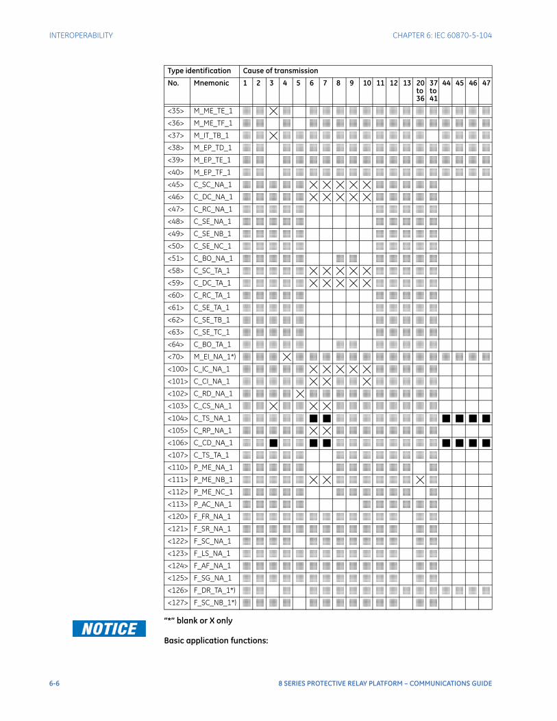
INTEROPERABILITY CHAPTER 6: IEC 60870-5-104
FASTPATH: “*” blank or X only
Basic application functions:
<35> M_ME_TE_1 ░ ░ ╳ ░ ░ ░ ░ ░ ░ ░ ░ ░ ░ ░ ░ ░ ░ ░<36> M_ME_TF_1 ░ ░ ░ ░ ░ ░ ░ ░ ░ ░ ░ ░ ░ ░ ░ ░ ░<37> M_IT_TB_1 ░ ░ ╳ ░ ░ ░ ░ ░ ░ ░ ░ ░ ░ ░ ░ ░ ░ ░<38> M_EP_TD_1 ░ ░ ░ ░ ░ ░ ░ ░ ░ ░ ░ ░ ░ ░ ░ ░ ░ ░<39> M_EP_TE_1 ░ ░ ░ ░ ░ ░ ░ ░ ░ ░ ░ ░ ░ ░ ░ ░ ░ ░<40> M_EP_TF_1 ░ ░ ░ ░ ░ ░ ░ ░ ░ ░ ░ ░ ░ ░ ░ ░ ░ ░<45> C_SC_NA_1 ░ ░ ░ ░ ░ ╳ ╳ ╳ ╳ ╳ ░ ░ ░ ░ ░<46> C_DC_NA_1 ░ ░ ░ ░ ░ ╳ ╳ ╳ ╳ ╳ ░ ░ ░ ░ ░<47> C_RC_NA_1 ░ ░ ░ ░ ░ ░ ░ ░ ░ ░<48> C_SE_NA_1 ░ ░ ░ ░ ░ ░ ░ ░ ░ ░<49> C_SE_NB_1 ░ ░ ░ ░ ░ ░ ░ ░ ░ ░<50> C_SE_NC_1 ░ ░ ░ ░ ░ ░ ░ ░ ░ ░<51> C_BO_NA_1 ░ ░ ░ ░ ░ ░ ░ ░ ░ ░ ░ ░<58> C_SC_TA_1 ░ ░ ░ ░ ░ ╳ ╳ ╳ ╳ ╳ ░ ░ ░ ░ ░<59> C_DC_TA_1 ░ ░ ░ ░ ░ ╳ ╳ ╳ ╳ ╳ ░ ░ ░ ░ ░<60> C_RC_TA_1 ░ ░ ░ ░ ░ ░ ░ ░ ░ ░<61> C_SE_TA_1 ░ ░ ░ ░ ░ ░ ░ ░ ░ ░<62> C_SE_TB_1 ░ ░ ░ ░ ░ ░ ░ ░ ░ ░<63> C_SE_TC_1 ░ ░ ░ ░ ░ ░ ░ ░ ░ ░<64> C_BO_TA_1 ░ ░ ░ ░ ░ ░ ░ ░ ░ ░ ░ ░<70> M_EI_NA_1*) ░ ░ ░ ╳ ░ ░ ░ ░ ░ ░ ░ ░ ░ ░ ░ ░ ░ ░ ░<100> C_IC_NA_1 ░ ░ ░ ░ ░ ╳ ╳ ╳ ╳ ╳ ░ ░ ░ ░ ░<101> C_CI_NA_1 ░ ░ ░ ░ ░ ╳ ╳ ░ ░ ╳ ░ ░ ░ ░ ░<102> C_RD_NA_1 ░ ░ ░ ░ ╳ ░ ░ ░ ░ ░ ░ ░ ░ ░ ░<103> C_CS_NA_1 ░ ░ ╳ ░ ░ ╳ ╳ ░ ░ ░ ░ ░ ░ ░ ░<104> C_TS_NA_1 ░ ░ ░ ░ ░ █ █ ░ ░ ░ ░ ░ ░ ░ ░ █ █ █ █<105> C_RP_NA_1 ░ ░ ░ ░ ░ ╳ ╳ ░ ░ ░ ░ ░ ░ ░ ░<106> C_CD_NA_1 ░ ░ █ ░ ░ █ █ ░ ░ ░ ░ ░ ░ ░ ░ █ █ █ █<107> C_TS_TA_1 ░ ░ ░ ░ ░ ░ ░ ░ ░ ░ ░ ░ ░<110> P_ME_NA_1 ░ ░ ░ ░ ░ ░ ░ ░ ░ ░ ░ ░<111> P_ME_NB_1 ░ ░ ░ ░ ░ ╳ ╳ ░ ░ ░ ░ ░ ░ ╳ ░<112> P_ME_NC_1 ░ ░ ░ ░ ░ ░ ░ ░ ░ ░ ░ ░<113> P_AC_NA_1 ░ ░ ░ ░ ░ ░ ░ ░ ░ ░ ░<120> F_FR_NA_1 ░ ░ ░ ░ ░ ░ ░ ░ ░ ░ ░ ░ ░ ░<121> F_SR_NA_1 ░ ░ ░ ░ ░ ░ ░ ░ ░ ░ ░ ░ ░ ░<122> F_SC_NA_1 ░ ░ ░ ░ ░ ░ ░ ░ ░ ░ ░ ░ ░<123> F_LS_NA_1 ░ ░ ░ ░ ░ ░ ░ ░ ░ ░ ░ ░ ░ ░<124> F_AF_NA_1 ░ ░ ░ ░ ░ ░ ░ ░ ░ ░ ░ ░ ░ ░<125> F_SG_NA_1 ░ ░ ░ ░ ░ ░ ░ ░ ░ ░ ░ ░ ░ ░<126> F_DR_TA_1*) ░ ░ ░ ░ ░ ░ ░ ░ ░ ░ ░ ░ ░ ░ ░ ░ ░<127> F_SC_NB_1*) ░ ░ ░ ░ ░ ░ ░ ░ ░ ░ ░ ░ ░
Type identification Cause of transmission
No. Mnemonic 1 2 3 4 5 6 7 8 9 10 11 12 13 20 to 36
37 to 41
44 45 46 47
6-6 8 SERIES PROTECTIVE RELAY PLATFORM – COMMUNICATIONS GUIDE
CHAPTER 6: IEC 60870-5-104 INTEROPERABILITY
Station initialization:⊠ Remote initialization.Cyclic data transmission:⊠ Cyclic data transmission.Read procedure:⊠ Read procedure.Spontaneous transmission:⊠ Spontaneous transmission.Double transmission of information objects with cause of transmission spontaneous:The following type identifications may be transmitted in succession caused by a single status change of an information object. The particular information object addresses for which double transmission is enabled are defined in a project-specific list.□ Single point information: M_SP_NA_1, M_SP_TA_1, M_SP_TB_1, and M_PS_NA_1.□ Double point information: M_DP_NA_1, M_DP_TA_1, and M_DP_TB_1.□ Step position information: M_ST_NA_1, M_ST_TA_1, and M_ST_TB_1.□ Bitstring of 32 bits: M_BO_NA_1, M_BO_TA_1, and M_BO_TB_1 (if defined for a specific project).□ Measured value, normalized value: M_ME_NA_1, M_ME_TA_1, M_ME_ND_1, and M_ME_TD_1.□ Measured value, scaled value: M_ME_NB_1, M_ME_TB_1, and M_ME_TE_1.□ Measured value, short floating point number: M_ME_NC_1, M_ME_TC_1, and M_ME_TF_1.Station interrogation:⊠ Group 1.⊠ Group 2.⊠ Group 3.⊠ Group 4.⊠ Group 5.⊠ Group 6.⊠ Group 7.⊠ Group 8.⊠ Group 9.⊠ Group 10.⊠ Group 11.⊠ Group 12.⊠ Group 13.⊠ Group 14.⊠ Group 15.⊠ Group 16.⊠ Global.Clock synchronization:⊠ Clock synchronization (optional, see Clause 7.6).□ Day of week used.□ RESI, GEN (time tag substituted/not substituted)□ SU-bit (summertime) used.Command transmission:⊠ Direct command transmission.□ Direct setpoint command transmission.⊠ Select and execute command.
8 SERIES PROTECTIVE RELAY PLATFORM – COMMUNICATIONS GUIDE 6-7
INTEROPERABILITY CHAPTER 6: IEC 60870-5-104
□ Select and execute setpoint command.⊠ C_SE ACTTERM used.⊠ No additional definition.⊠ Short pulse duration (duration determined by a system parameter in the outstation).⊠ Long pulse duration (duration determined by a system parameter in the outstation).⊠ Persistent output.⊠ Supervision of maximum delay in command direction of commands and setpoint commands.Maximum allowable delay of commands and setpoint commands: 5 s.Transmission of integrated totals:⊠ Mode A: Local freeze with spontaneous transmission.⊠ Mode B: Local freeze with counter interrogation.⊠ Mode C: Freeze and transmit by counter-interrogation commands.⊠ Mode D: Freeze by counter-interrogation command, frozen values reported simultaneously.⊠ Counter read.⊠ Counter freeze without reset.⊠ Counter freeze with reset.⊠ Counter reset.⊠ General request counter.⊠ Request counter group 1.⊠ Request counter group 2.⊠ Request counter group 3.⊠ Request counter group 4.Parameter loading:⊠ Threshold value.□ Smoothing factor.□ Low limit for transmission of measured values.□ High limit for transmission of measured values.Parameter activation:□ Activation/deactivation of persistent cyclic or periodic transmission of the addressed object.Test procedure:□ Test procedure.File transfer in monitor direction:□ Transparent file.□ Transmission of disturbance data of protection equipment.□ Transmission of sequences of events.□ Transmission of sequences of recorded analog values.File transfer in control direction:□ Transparent file.Background scan:□ Background scan.Definition of timeouts:
6-8 8 SERIES PROTECTIVE RELAY PLATFORM – COMMUNICATIONS GUIDE
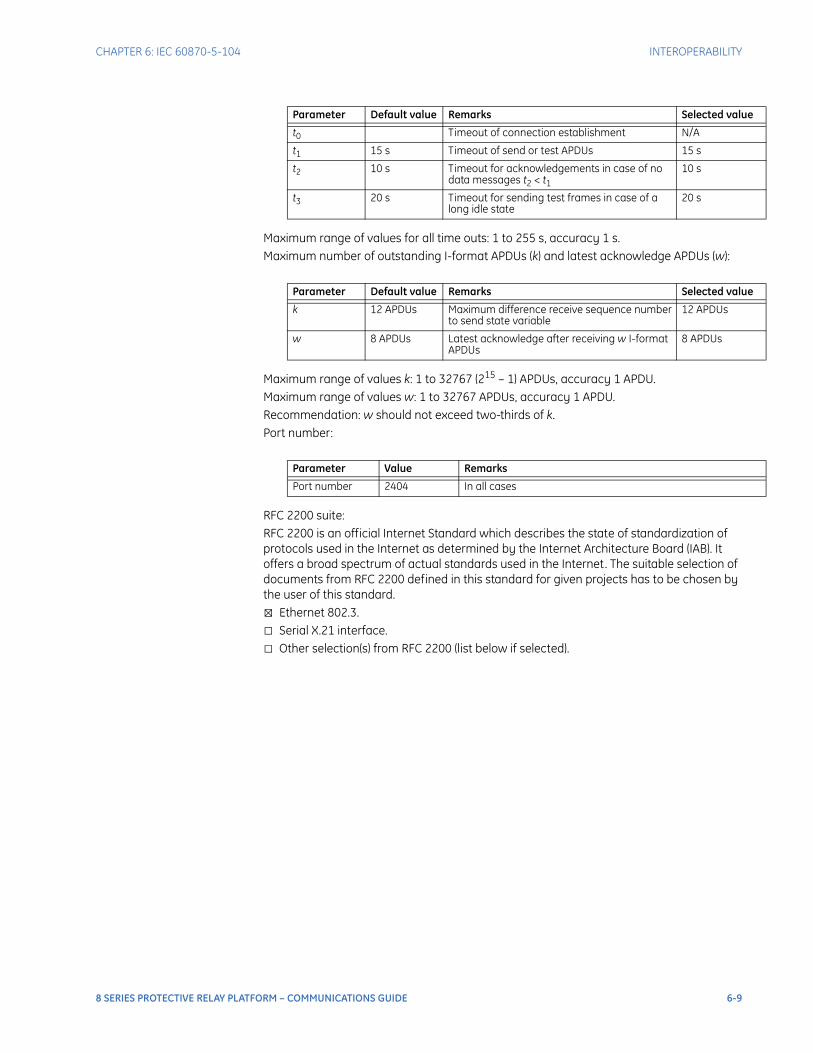
CHAPTER 6: IEC 60870-5-104 INTEROPERABILITY
Maximum range of values for all time outs: 1 to 255 s, accuracy 1 s.Maximum number of outstanding I-format APDUs (k) and latest acknowledge APDUs (w):
Maximum range of values k: 1 to 32767 (215 – 1) APDUs, accuracy 1 APDU.Maximum range of values w: 1 to 32767 APDUs, accuracy 1 APDU.Recommendation: w should not exceed two-thirds of k.Port number:
RFC 2200 suite:RFC 2200 is an official Internet Standard which describes the state of standardization of protocols used in the Internet as determined by the Internet Architecture Board (IAB). It offers a broad spectrum of actual standards used in the Internet. The suitable selection of documents from RFC 2200 defined in this standard for given projects has to be chosen by the user of this standard.⊠ Ethernet 802.3.□ Serial X.21 interface.□ Other selection(s) from RFC 2200 (list below if selected).
Parameter Default value Remarks Selected value
t0 Timeout of connection establishment N/A
t1 15 s Timeout of send or test APDUs 15 s
t2 10 s Timeout for acknowledgements in case of no data messages t2 < t1
10 s
t3 20 s Timeout for sending test frames in case of a long idle state
20 s
Parameter Default value Remarks Selected value
k 12 APDUs Maximum difference receive sequence number to send state variable
12 APDUs
w 8 APDUs Latest acknowledge after receiving w I-format APDUs
8 APDUs
Parameter Value Remarks
Port number 2404 In all cases
8 SERIES PROTECTIVE RELAY PLATFORM – COMMUNICATIONS GUIDE 6-9

INTEROPERABILITY CHAPTER 6: IEC 60870-5-104
6-10 8 SERIES PROTECTIVE RELAY PLATFORM – COMMUNICATIONS GUIDE
8 Series Protective Relay Platform
Chapter 7: IEC 60870-5-103
GEGrid Solutions
IEC 60870-5-103
The point map for the 103 is different from the one shared by the IEC104 and DNP protocols. IEC 60870-5-103 serial communications protocol is supported on the rear RS485 port only.The DNP, 103 and Modbus can not be enabled simultaneously. Only one instance of DNP3.0, IEC 103 or Modbus can run on the RS485 serial port.Path: Setpoints > Device > Communications > IEC60870-5-103
To view the list of binary inputs, see the 8 Series relay Flexlogic Operands table in the Setpoints/ FlexLogic section of the individual 8 Series relay instruction manual.
FASTPATH: The user must pay attention when configuring the function type and information number of the different points, because they must be unique. There is no mechanism in the EnerVista 8 Series Setup software or the front panel HMI to detect duplication of the information index.
FASTPATH: The IEC 60870-5-103 point lists always begin with point 0 and end at the first “Off” value. Since IEC 60870-5-103 point lists must be in one continuous block, any points assigned after the first “Off” point are ignored.
Cause of Transmission
The cause of transmission is an unsigned integer which takes one of the values specified in the following tables.
Table 7-1: Cause of Transmission in the Monitor Direction
Value Description
<1> Spontaneous
<2> Cyclic
<3> Reset frame count bit (FCB)
<4> Reset communications unit (CU)
<5> Start/Restart
<6> Power on
<8> Time synchronization
8 SERIES PROTECTIVE RELAY PLATFORM – COMMUNICATIONS GUIDE 7-1
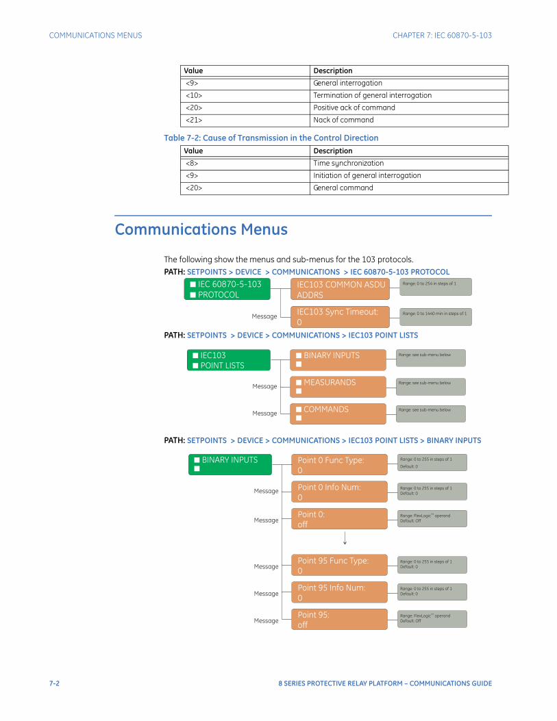
COMMUNICATIONS MENUS CHAPTER 7: IEC 60870-5-103
Table 7-2: Cause of Transmission in the Control Direction
Communications Menus
The following show the menus and sub-menus for the 103 protocols.PATH: SETPOINTS > DEVICE > COMMUNICATIONS > IEC 60870-5-103 PROTOCOL
PATH: SETPOINTS > DEVICE > COMMUNICATIONS > IEC103 POINT LISTS
PATH: SETPOINTS > DEVICE > COMMUNICATIONS > IEC103 POINT LISTS > BINARY INPUTS
<9> General interrogation
<10> Termination of general interrogation
<20> Positive ack of command
<21> Nack of command
Value Description
<8> Time synchronization
<9> Initiation of general interrogation
<20> General command
Value Description
Message
Range: see sub-menu below■ IEC103■ POINT LISTS
Range: see sub-menu below
■ BINARY INPUTS■
■ MEASURANDS■
MessageRange: see sub-menu below■ COMMANDS
■
Message
Range: 0 to 255 in steps of 1
Default: 0
■ BINAR INPUTS■
Point 0 Func Type:0
Point 0 Info Num:0
MessagePoint 0:off
Range: 0 to 255 in steps of 1Default: 0
MessagePoint 95 Func Type:0
Range: 0 to 255 in steps of 1Default: 0
MessagePoint 95 Info Num:0
Range: 0 to 255 in steps of 1Default: 0
MessagePoint 95:off
Range: FlexLogic operandDefault: Off
TM
Range: FlexLogic operandDefault: Off
TM
7-2 8 SERIES PROTECTIVE RELAY PLATFORM – COMMUNICATIONS GUIDE
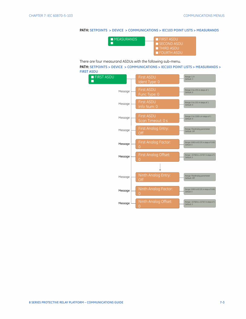
CHAPTER 7: IEC 60870-5-103 COMMUNICATIONS MENUS
PATH: SETPOINTS > DEVICE > COMMUNICATIONS > IEC103 POINT LISTS > MEASURANDS
There are four measurand ASDUs with the following sub-menu.PATH: SETPOINTS > DEVICE > COMMUNICATIONS > IEC103 POINT LISTS > MEASURANDS > FIRST ASDU
■ MEASURANDS■
■ FIRST ASDU■
■
■
SECOND ASDUTHIRD ASDUFOURTH ASDU
8 SERIES PROTECTIVE RELAY PLATFORM – COMMUNICATIONS GUIDE 7-3
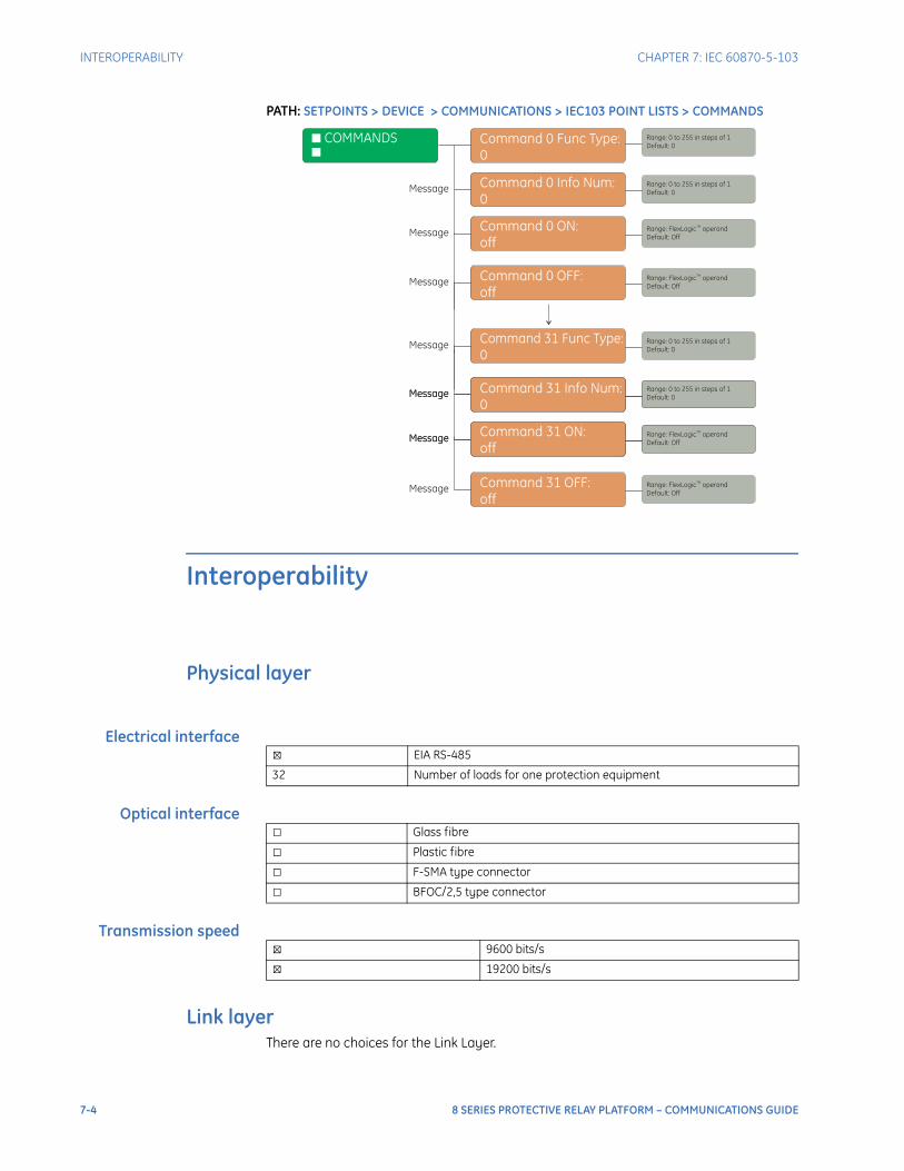
INTEROPERABILITY CHAPTER 7: IEC 60870-5-103
PATH: SETPOINTS > DEVICE > COMMUNICATIONS > IEC103 POINT LISTS > COMMANDS
Interoperability
Physical layer
Electrical interface
Optical interface
Transmission speed
Link layerThere are no choices for the Link Layer.
Message
■ COMMANDS■
Command 0 Func Type:0
Message
Range: 0 to 255 in steps of 1Default: 0
Message
Message
Message
Command 0 ON:off
Command 0 Info Num:0
Range: 0 to 255 in steps of 1Default: 0
Range: 0 to 255 in steps of 1Default: 0
First Analog Factor:0
Message
MessageRange: 0 to 255 in steps of 1Default: 0
First Analog Factor:0
Message
Message Range: FlexLogic operandDefault: Off
TM
Command 0 OFF:off
Command 31 Func Type:0
Command 31 ON:off
Command 31 Info Num:0
Command 31 OFF:off
Range: FlexLogic operandDefault: Off
TM
Range: 0 to 255 in steps of 1Default: 0
Range: 0 to 255 in steps of 1Default: 0
Range: FlexLogic operandDefault: Off
TM
Range: FlexLogic operandDefault: Off
TM
⊠ EIA RS-485
32 Number of loads for one protection equipment
□ Glass fibre
□ Plastic fibre
□ F-SMA type connector
□ BFOC/2,5 type connector
⊠ 9600 bits/s
⊠ 19200 bits/s
7-4 8 SERIES PROTECTIVE RELAY PLATFORM – COMMUNICATIONS GUIDE
CHAPTER 7: IEC 60870-5-103 INTEROPERABILITY
Application layer
Transmission mode for application data
Mode 1 (least significant octet first), is used exclusively in this companion standard.
Common address of ASDU
Selection of standard information numbers
in monitor direction
Table 7-3: System functions in monitor direction
Table 7-4: Status indications in monitor direction
Table 7-5: Supervision indications in monitor direction
⊠ One COMMON ADDRESS OF ASDU (identical with station address)
More than one COMMON ADDRESS OF ASDU
INF Semantics
⊠ <0> End of general interrogation
⊠ <0> Time synchronization
⊠ <2> Reset FCB
⊠ <3> Reset CU
⊠ <4> Start/restart
⊠ <5> Power on
INF Semantics 8 Series relay Identifier
8 Series relay Data Text
□ <16> Auto-recloser active
□ <17> Teleprotection active
□ <18> Protection active
□ <19> LED reset
□ <20> Monitor direction blocked
□ <21> Test mode
□ <22> Local parameter setting
□ <23> Characteristic 1
□ <24> Characteristic 2
□ <25> Characteristic 3
□ <26> Characteristic 4
□ <27> Auxiliary input 1
□ <28> Auxiliary input 2
□ <29> Auxiliary input 3
□ <30> Auxiliary input 4
INF Semantics 8 Series relay Identifier
8 Series relay Data Text
□ <32> Measurand supervision I
□ <33> Measurand supervision V
□ <35> Phase sequence supervision
□ <36> Trip circuit supervision
□ <37> I>> back-up operation
□ <38> VT fuse failure
8 SERIES PROTECTIVE RELAY PLATFORM – COMMUNICATIONS GUIDE 7-5
INTEROPERABILITY CHAPTER 7: IEC 60870-5-103
Table 7-6: Earth fault indications in monitor direction
Table 7-7: Fault indications in monitor direction
□ <39> Teleprotection disturbed
□ <46> Group warning
□ <47> Group alarm
INF Semantics 8 Series relay Identifier
8 Series relay Data Text
□ <48> Earth fault L1
□ <49> Earth fault L2
□ <50> Earth fault L3
□ <51> Earth fault forward, i.e. line
□ <52> Earth fault reverse, i.e. busbar
INF Semantics 8 Series relay Identifier
8 Series relay Data Text
□ <64> Start / pick-up L1
□ <65> Start / pick-up L2
□ <66> Start / pick-up L3
□ <67> Start / pick-up N
□ <68> General trip
□ <69> Trip L1
□ <70> Trip L2
□ <71> Trip L3
□ <72> Trip I>> (back-up operation)
□ <73> Fault location X in ohms
□ <74> Fault forward / line
□ <75> Fault reverse / busbar
□ <76> Teleprotection signal transmitted
□ <77> Teleprotection signal received
□ <78> Zone 1
□ <79> Zone 2
□ <80> Zone 3
□ <81> Zone 4
□ <82> Zone 5
□ <83> Zone 6
□ <84> General start / pick-up
□ <85> Breaker failure
□ <86> Trip measuring system L1
□ <87> Trip measuring system L2
□ <88> Trip measuring system L3
□ <89> Trip measuring system E
□ <90> Trip I>
□ <91> Trip I>>
□ <92> Trip IN>
□ <93> Trip IN>>
INF Semantics 8 Series relay Identifier
8 Series relay Data Text
7-6 8 SERIES PROTECTIVE RELAY PLATFORM – COMMUNICATIONS GUIDE
CHAPTER 7: IEC 60870-5-103 INTEROPERABILITY
Table 7-8: Auto-reclosure indications in monitor direction
Table 7-9: Measurands in monitor direction
Table 7-10: Generic functions in monitor direction
Selection of standard information numbers
in control direction
Table 7-11: System functions in control direction
Table 7-12: General commands in control direction
Table 7-13: General functions in control direction
INF Semantics 8 Series relay Identifier
8 Series relay Data Text
□ <128> CB ‘on’ by AR
□ <129> CB ‘on’ by long-time AR
□ <130> AR blocked
INF Semantics 8 Series relay Identifier
8 Series relay Data Text
□ <144> Measurand I
□ <145> Measurands I, V
□ <146> Measurands I, V, P, Q
□ <147> Measurands In, Ven
□ <148> Measurands IL123, VL123, P, Q, f
INF Semantics
□ <240> Read headings of all defined groups
□ <241> Read values or attributes of all entries of one group
□ <243> Read directory of a single entry
□ <244> Read value or attribute of a single entry
□ <245> End of general interrogation of generic data
□ <249> Write entry with confirmation
□ <250> Write entry with execution
□ <251> Write entry aborted
INF Semantics
⊠ <0> Initiation of general interrogation
⊠ <0> Time synchronization
INF Semantics
□ <16> Auto-recloser on / off
□ <17> Teleprotection on / off
□ <18> Protection on / off
□ <19> LED reset
□ <23> Activate characteristic 1
□ <24> Activate characteristic 2
□ <25> Activate characteristic 3
□ <26> Activate characteristic 4
INF Semantics
□ <240> Read headings of all defined groups
□ <241> Read values or attributes of all entries of one group
□ <243> Read directory of a single entry
□ <244> Read value or attribute of a single entry
□ <245> General interrogation of generic data
8 SERIES PROTECTIVE RELAY PLATFORM – COMMUNICATIONS GUIDE 7-7
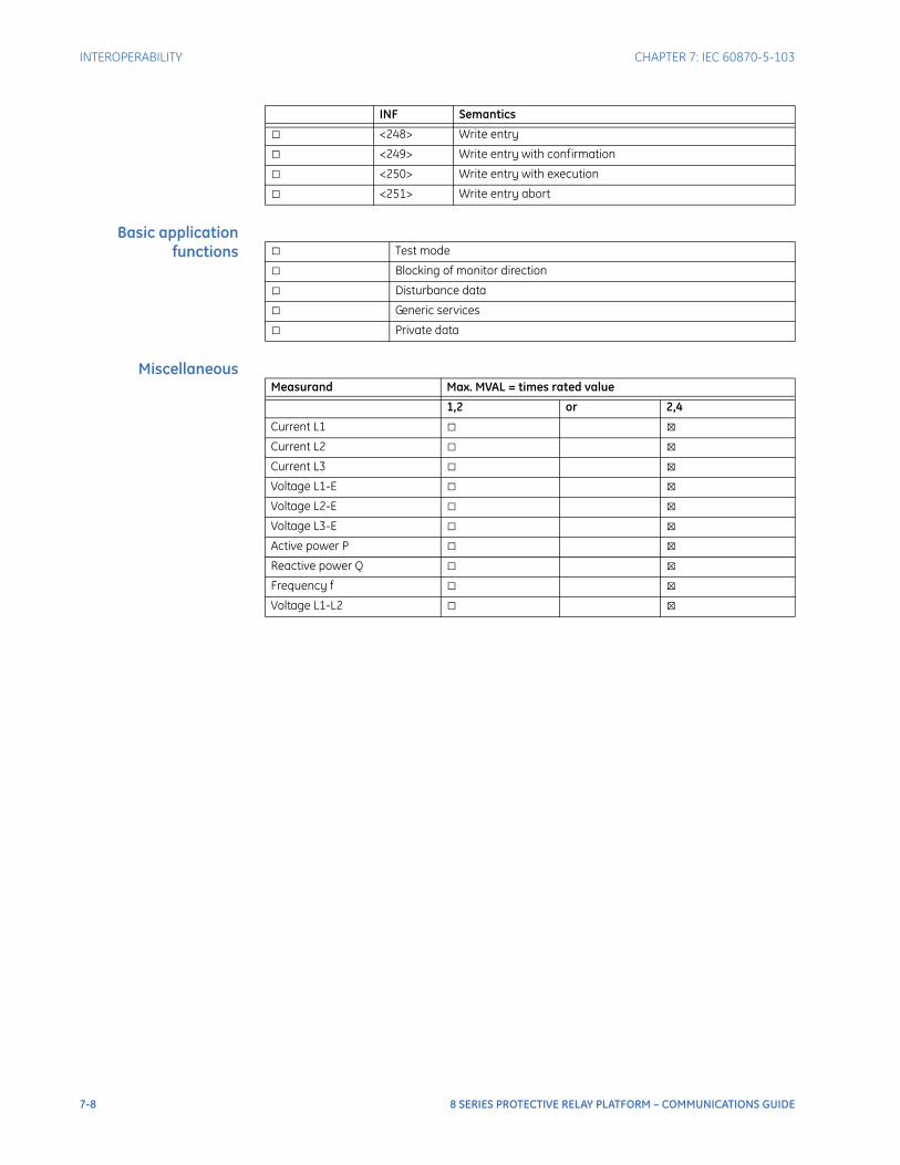
INTEROPERABILITY CHAPTER 7: IEC 60870-5-103
Basic application functions
Miscellaneous
□ <248> Write entry
□ <249> Write entry with confirmation
□ <250> Write entry with execution
□ <251> Write entry abort
INF Semantics
□ Test mode
□ Blocking of monitor direction
□ Disturbance data
□ Generic services
□ Private data
Measurand Max. MVAL = times rated value
1,2 or 2,4
Current L1 □ ⊠Current L2 □ ⊠Current L3 □ ⊠Voltage L1-E □ ⊠Voltage L2-E □ ⊠Voltage L3-E □ ⊠Active power P □ ⊠Reactive power Q □ ⊠Frequency f □ ⊠Voltage L1-L2 □ ⊠
7-8 8 SERIES PROTECTIVE RELAY PLATFORM – COMMUNICATIONS GUIDE
8 Series Protective Relay Platform
Chapter 8: IEC 61850
GEGrid Solutions
IEC 61850
The optional communications processor supports both the IEC61850 GOOSE and IEC 61850 MMS Server service as per IEC 61850 standard Ed. 2. The GOOSE messaging service provides the 8 Series relay unit the ability to Publish/Subscribe Digital Input Status and its Quality and Timestamp to/from other IEDs with supporting GOOSE messaging service, while the server support allows remote control center, RTU/Gateway, local HMI or other client role devices access to the relay for monitoring and control. The configuration of IEC61850 services is accomplished using the 8 Series relay configuration software, EnerVista 8 Series Setup software. A rebooting MUST be done before any changes made take affect.
General
IEC61850 SERVERThe IEC 61850 Server (i.e., 8 Series relay) reports data to the IEC 61850 Client, such as Local HMI, RTU and Gateway with the information of logical device, data sets, data control block, logical nodes and their data attributes.The following tables list the logical nodes and number of instances for each of the LNs that are supported within the 8 Series relay.LOGICAL NODES
Table 8-1: Communications Elements in the 8 Series relay
8 Series relay Communications Elements Corresponding IEC61850 Logical node and number of instances
Supported in 8 Series relay
Port status LCCH (3)
Remote Device LGOS (8) Yes
Time master supervision LTMS
Time management LTIM
PHYSICAL DEVICE INFORMATION LPHD Yes
Logical Node 0 LLN0 Yes
8 SERIES PROTECTIVE RELAY PLATFORM – COMMUNICATIONS GUIDE 8-1
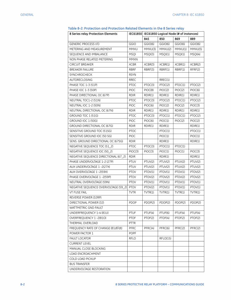
GENERAL CHAPTER 8: IEC 61850
Table 8-2: Protection and Protection Related Elements in the 8 Series relay
8 Series relay Protection Elements IEC61850 IEC61850 Logical Node (# of instances)
845 850 869 889
GENERIC PROCESS I/O GGIO GGIO(6) GGIO(6) GGIO(6) GGIO(6)
METERING AND MEASUREMENT MMXU MMXU(3) MMXU(2) MMXU(1) MMXU(5)
SEQUENCE AND IMBALANCE MSQI MSQI(3) MSQI(1) MSQI(1) MSQI(4)
NON PHASE RELATED METERING MMXN
CIRCUIT BREAKER XCBR XCBR(3) XCBR(1) XCBR(1) XCBR(2)
BREAKER FAILURE RBRF RBRF(3) RBRF(1) RBRF(1) RFRF(2)
SYNCHROCHECK RSYN
AUTORECLOSING RREC RREC(1)
PHASE TOC 1-3 (51P) PTOC PTOC(3) PTOC(2) PTOC(1) PTOC(2)
PHASE IOC 1-3 (50P) PIOC PIOC(8) PIOC(2) PIOC(2) PIOC(6)
PHASE DIRECTIONAL OC (67P) RDIR RDIR(1) RDIR(1) RDIR(1) RDIR(1)
NEUTRAL TOC1-2 (51N) PTOC PTOC(3) PTOC(2) PTOC(1) PTOC(2)
NEUTRAL IOC 1-2 (50N) PIOC PIOC(6) PIOC(2) PIOC(2) PIOC(3)
NEUTRAL DIRECTIONAL OC (67N) RDIR RDIR(1) RDIR(1) RDIR(1) RDIR(1)
GROUND TOC 1 (51G) PTOC PTOC(3) PTOC(1) PTOC(1) PTOC(2)
GROUND IOC 1 (50G) PIOC PIOC(6) PIOC(1) PIOC(2) PIOC(2)
GROUND DIRECTIONAL OC (67G) RDIR RDIR(1) RDIR(1) RDIR(1)
SENSITIVE GROUND TOC (51SG) PTOC PTOC(1) PTOC(1)
SENSITIVE GROUND IOC (50 SG) PIOC PIOC(1) PIOC(1)
SENS. GROUND DIRECTIONAL OC (67SG) RDIR RDIR(1) RDIR(1)
NEGATIVE SEQUENCE TOC (51_2) PTOC PTOC(3) PTOC(1) PTOC(1)
NEGATIVE SEQUENCE IOC (50_2) PIOC(3) PIOC(3) PIOC(1) PIOC(1) PIOC(3)
NEGATIVE SEQUENCE DIRECTIONAL (67_2) RDIR RDIR(1) RDIR(1)
PHASE UNDERVOLTAGE 1-2 (27P) PTUV PTUV(2) PTUV(2) PTUV(2) PTUV(2)
AUX UNDERVOLTAGE 1 -2(27X) PTUV PTUV(2) PTUV(2) PTUV(2) PTUV(2)
AUX OVERVOLTAGE 1 -2(59X) PTOV PTOV(1) PTOV(1) PTOV(1) PTOV(2)
PHASE OVERVOLTAGE 1 -2(59P) PTOV PTOV(2) PTOV(2) PTOV(2) PTOV(2)
NEUTRAL OVERVOLTAGE (59N) PTOV PTOV(1) PTOV(1) PTOV(1) PTOV(1)
NEGATIVE SEQUENCE OVERVOLTAGE (59_2) PTOV PTOV(2) PTOV(1) PTOV(1) PTOV(1)
VT FUSE FAIL TVTR TVTR(1) TVTR(1) TVTR(1) TVTR(1)
REVERSE POWER (32RP)
DIRECTIONAL POWER (32) PDOP PDOP(2) PDOP(2) PDOP(2) PDOP(2)
WATTMETRIC GND FAULT
UNDERFREQUENCY 1-4 (81U) PTUF PTUF(4) PTUF(6) PTUF(4) PTUF(4)
OVERFREQUENCY 1 -2(81O) PTOF PTOF(2) PTOF(4) PTOF(2) PTOF(2)
THERMAL OVERLOAD PTTR
FREQUENCY RATE OF CHANGE (81df/dt) PFRC PFRC(4) PFRC(6) PFRC(2) PFRC(2)
POWER FACTOR 1 POPF
FAULT LOCATOR RFLO RFLO(15)
CURRENT LEVEL
MANUAL CLOSE BLOCKING
LOAD ENCROACHMENT
COLD LOAD PICKUP
BUS TRANSFER
UNDERVOLTAGE RESTORATION
8-2 8 SERIES PROTECTIVE RELAY PLATFORM – COMMUNICATIONS GUIDE

CHAPTER 8: IEC 61850 GENERAL
NOTE
NOTE: The Generic IO is mapped to GGIO nodes as follows: GGIO1 – This logical node is mapped to “Remote outputs”. 8 Series supports 32 remote outputs. The User can configure them in the IEC61850 Configurator -> “Settings” tab GGIO2 – This logical node is mapped to “Contact input” in the 8 Series GGIO3 – This logical node is mapped to “Virtual input”. 8 Series supports 32 virtual inputs. The User can configure virtual inputs in 8 Series setpoints -> Input -> Virtual Inputs. GGIO4 – This logical node is mapped to “Virtual output”. 8 Series supports upto 32 Virtual outputs. The User can configure virtual outputs using the FlexLogic / Logic Designer feature GGIO5 – This logical node is mapped to “Remote input”. 8 Series supports upto 32 remote inputs. The User can configure remote inputs in the IEC61850 configurator -> “GOOSE Reception” tab GGIO6 – Contact output / output relays
UNDERFREQUENCY RESTORATION
EARTH LEAKAGE PHIZ
RESTRICTED EARTH FAULT
LOAD ENCROACHMENT
BROKEN CONDUCTOR
CABLE THERMAL MODEL
TRIP BUS PTRC PTRC(6) PTRC(6) PTRC(6) PTRC(6)
RTD TTMP TTMP(13) TTMP(13) TTMP(13) TTMP(13)
W1 Xfmr Overload PTTR PTTR(1)
WINDING HOTTEST-SPOT TEMPERATURE PTTR PTTR(1)
XFRM INSTANT DIFFERENTIAL PDIF PDIF(1)
XFRM PERCENT DIFFERENTIAL PDIF PDIF(1)
VOLTS PER HERTZ PVPH PVPH(2) PVPH(2)
PHASE REVERSAL PTOV(1) PTOV(1)
CURRENT UNBALANCE PTOC(2) PTOC(2)
ACCELERATION TIME PTOC(1)
LOAD INCREASE PTOC(1) PTOC(1)
GROUND FAULT PIOC(2)
MECHANICAL JAM PIOC(1)
SHORT CIRCUIT PIOC(1)
THERMAL MODEL PTTR(1)
RESTART INHIBITED PMRI(1)
UNDERPOWER PDUP(2)
UNDERCURRENT PTUC(2)
STATOR DIFFERENTIAL PDIF(1)
THIRD HARMONIC NEUTRAL PTUV(1)
GENERATOR PERCENT DIFFERENTIAL PDIF(1)
OVERALL PERCENT DIFFERENTIAL PDIF(1)
LOSS OF EXCITATION PDIS(2)
OOS PPAM(1)
THERMAL OVERLOAD PTTR(1)
INADVERTENT ENERGIZATION PIOC(1)
OFFLINE OVERCURRENT PIOC(1)
8 Series relay Protection Elements IEC61850 IEC61850 Logical Node (# of instances)
845 850 869 889
8 SERIES PROTECTIVE RELAY PLATFORM – COMMUNICATIONS GUIDE 8-3
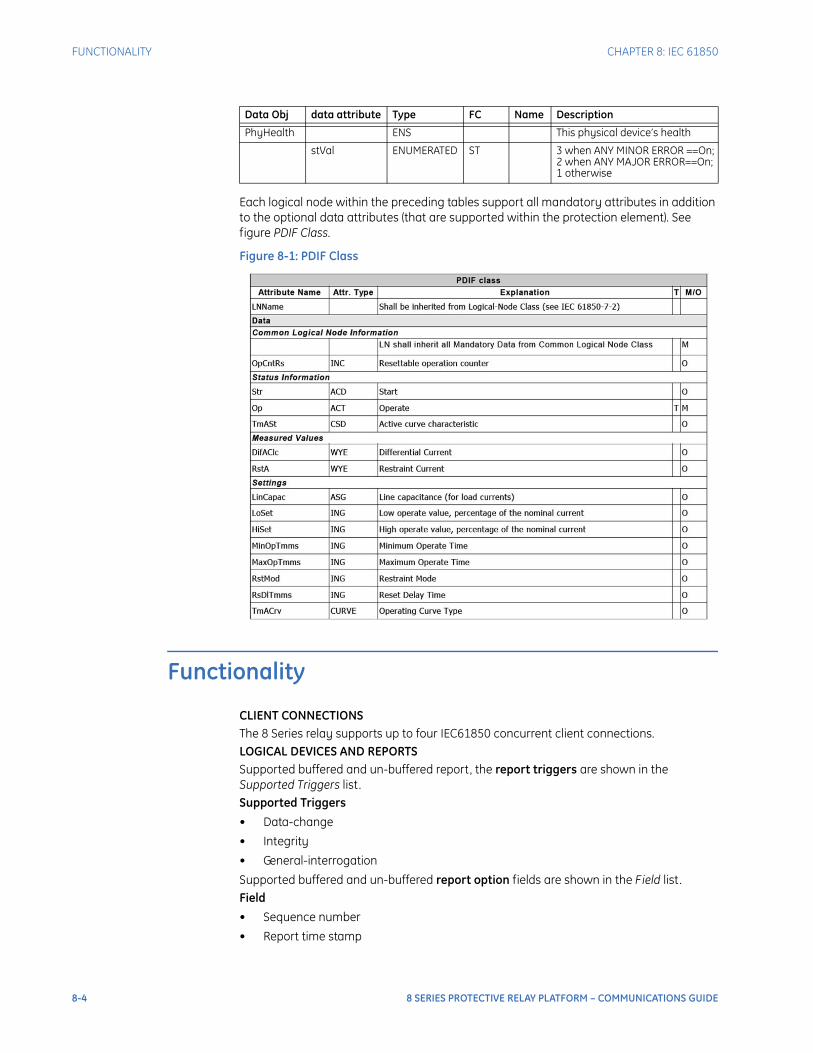
FUNCTIONALITY CHAPTER 8: IEC 61850
Each logical node within the preceding tables support all mandatory attributes in addition to the optional data attributes (that are supported within the protection element). See figure PDIF Class.
Figure 8-1: PDIF Class
Functionality
CLIENT CONNECTIONSThe 8 Series relay supports up to four IEC61850 concurrent client connections.LOGICAL DEVICES AND REPORTSSupported buffered and un-buffered report, the report triggers are shown in the Supported Triggers list.Supported Triggers
• Data-change
• Integrity
• General-interrogation
Supported buffered and un-buffered report option fields are shown in the Field list.Field
• Sequence number
• Report time stamp
Data Obj data attribute Type FC Name Description
PhyHealth ENS This physical device’s health
stVal ENUMERATED ST 3 when ANY MINOR ERROR ==On; 2 when ANY MAJOR ERROR==On; 1 otherwise
8-4 8 SERIES PROTECTIVE RELAY PLATFORM – COMMUNICATIONS GUIDE
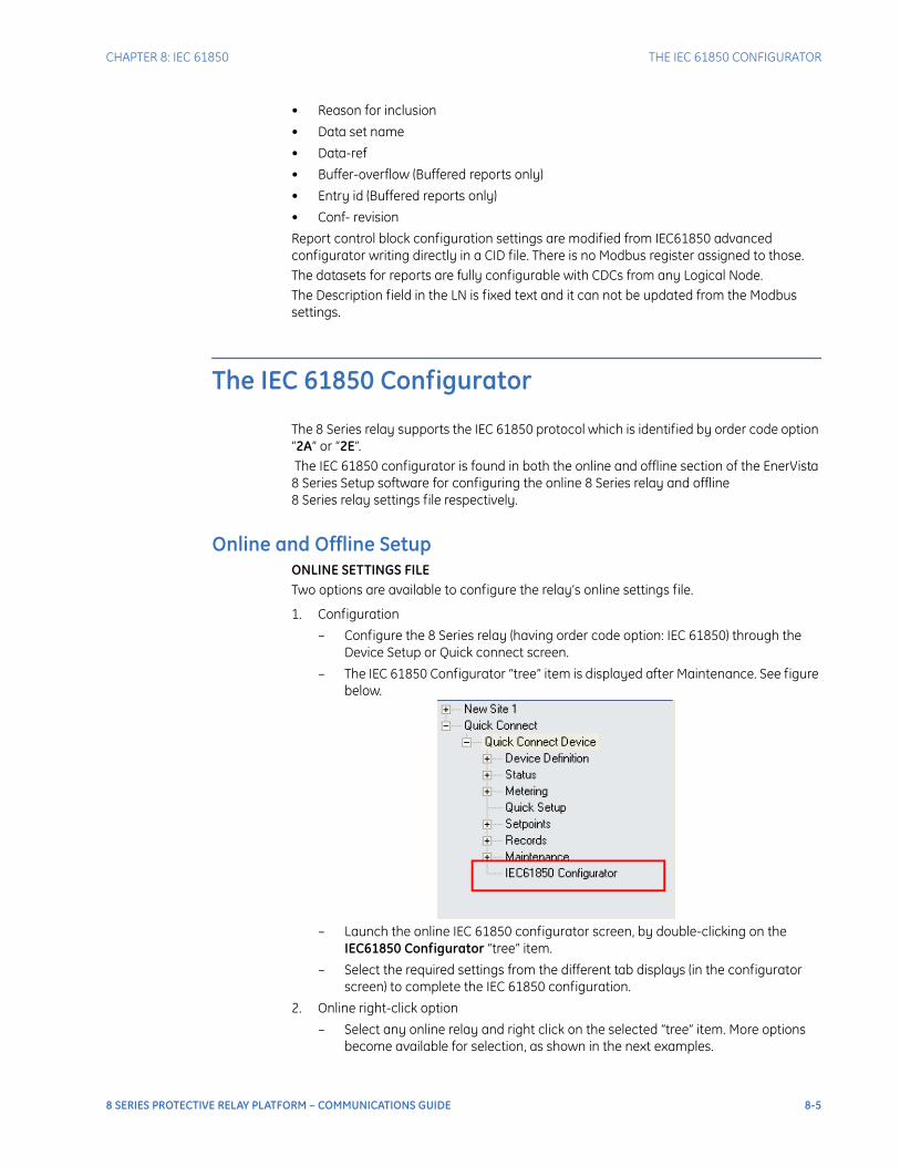
CHAPTER 8: IEC 61850 THE IEC 61850 CONFIGURATOR
• Reason for inclusion
• Data set name
• Data-ref
• Buffer-overflow (Buffered reports only)
• Entry id (Buffered reports only)
• Conf- revision
Report control block configuration settings are modified from IEC61850 advanced configurator writing directly in a CID file. There is no Modbus register assigned to those.The datasets for reports are fully configurable with CDCs from any Logical Node.The Description field in the LN is fixed text and it can not be updated from the Modbus settings.
The IEC 61850 Configurator
The 8 Series relay supports the IEC 61850 protocol which is identified by order code option “2A” or “2E”. The IEC 61850 configurator is found in both the online and offline section of the EnerVista 8 Series Setup software for configuring the online 8 Series relay and offline 8 Series relay settings file respectively.
Online and Offline SetupONLINE SETTINGS FILETwo options are available to configure the relay’s online settings file.
1. Configuration
– Configure the 8 Series relay (having order code option: IEC 61850) through the Device Setup or Quick connect screen.
– The IEC 61850 Configurator “tree” item is displayed after Maintenance. See figure below.
– Launch the online IEC 61850 configurator screen, by double-clicking on the IEC61850 Configurator “tree” item.
– Select the required settings from the different tab displays (in the configurator screen) to complete the IEC 61850 configuration.
2. Online right-click option
– Select any online relay and right click on the selected “tree” item. More options become available for selection, as shown in the next examples.
8 SERIES PROTECTIVE RELAY PLATFORM – COMMUNICATIONS GUIDE 8-5
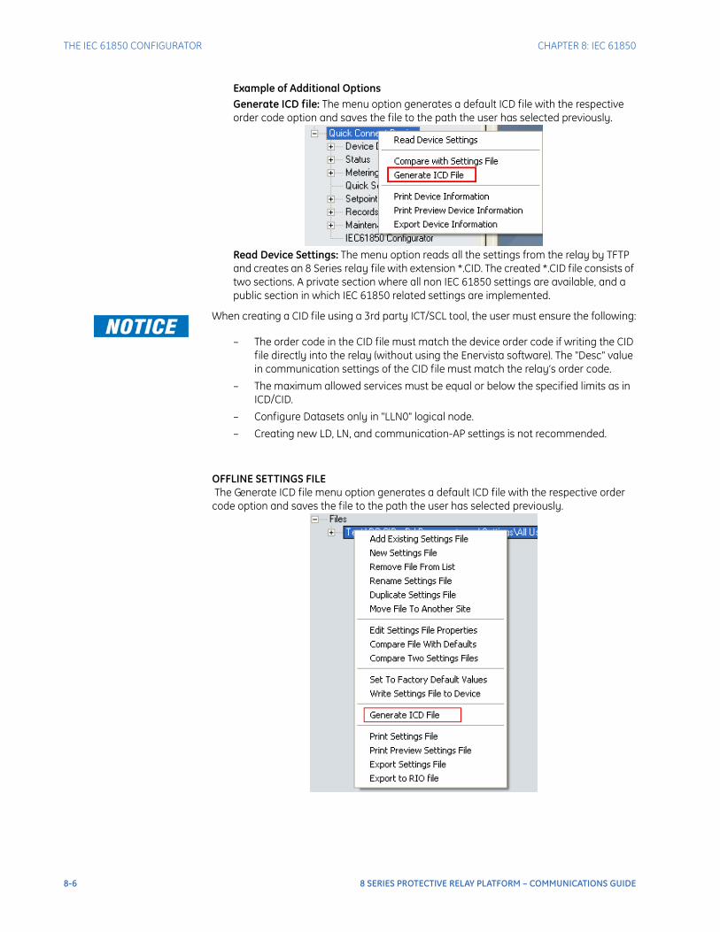
THE IEC 61850 CONFIGURATOR CHAPTER 8: IEC 61850
Example of Additional OptionsGenerate ICD file: The menu option generates a default ICD file with the respective order code option and saves the file to the path the user has selected previously.
Read Device Settings: The menu option reads all the settings from the relay by TFTP and creates an 8 Series relay file with extension *.CID. The created *.CID file consists of two sections. A private section where all non IEC 61850 settings are available, and a public section in which IEC 61850 related settings are implemented.
FASTPATH: When creating a CID file using a 3rd party ICT/SCL tool, the user must ensure the following:
– The order code in the CID file must match the device order code if writing the CID file directly into the relay (without using the Enervista software). The "Desc" value in communication settings of the CID file must match the relay’s order code.
– The maximum allowed services must be equal or below the specified limits as in ICD/CID.
– Configure Datasets only in "LLN0" logical node.
– Creating new LD, LN, and communication-AP settings is not recommended.
OFFLINE SETTINGS FILE The Generate ICD file menu option generates a default ICD file with the respective order code option and saves the file to the path the user has selected previously.
8-6 8 SERIES PROTECTIVE RELAY PLATFORM – COMMUNICATIONS GUIDE

CHAPTER 8: IEC 61850 THE IEC 61850 CONFIGURATOR
IEC 61850 Configurator DetailsThe IEC61850 Configurator allows the user to edit all sections of the IEC61850 CID and ICD file. The user cannot perform any other operations in the EnerVista 8 Series Setup software if the IEC 61850 Configurator is open. The user must close the IEC61850 session to perform other operations in the EnerVista software.The IEC 61850 configurator consists of five sections:
• ICD/CID
• Settings
• Reports
• GOOSE Reception
• GOOSE Transmission
ICD/CID Select the ICD/CID tab in the IEC 61850 Configurator window. The ICD/CID tab consists of the ICD Explorer window to the left side of the view. The ICD Explorer window allows the user to navigate through the data model of the relay and change desired IEC 61850 parameters such as the Logical Device Name, MMS port and others.
To Modify the Parameters
1. Select a parameter in the ICD Explorer window to open the Attributes window in the right part of the screen.
8 SERIES PROTECTIVE RELAY PLATFORM – COMMUNICATIONS GUIDE 8-7
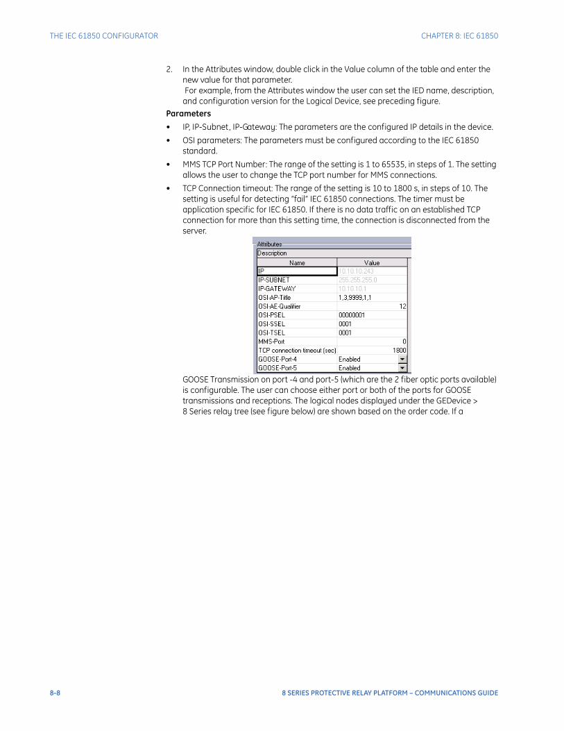
THE IEC 61850 CONFIGURATOR CHAPTER 8: IEC 61850
2. In the Attributes window, double click in the Value column of the table and enter the new value for that parameter. For example, from the Attributes window the user can set the IED name, description, and configuration version for the Logical Device, see preceding figure.
Parameters
• IP, IP-Subnet, IP-Gateway: The parameters are the configured IP details in the device.
• OSI parameters: The parameters must be configured according to the IEC 61850 standard.
• MMS TCP Port Number: The range of the setting is 1 to 65535, in steps of 1. The setting allows the user to change the TCP port number for MMS connections.
• TCP Connection timeout: The range of the setting is 10 to 1800 s, in steps of 10. The setting is useful for detecting “fail” IEC 61850 connections. The timer must be application specific for IEC 61850. If there is no data traffic on an established TCP connection for more than this setting time, the connection is disconnected from the server.
GOOSE Transmission on port -4 and port-5 (which are the 2 fiber optic ports available) is configurable. The user can choose either port or both of the ports for GOOSE transmissions and receptions. The logical nodes displayed under the GEDevice > 8 Series relay tree (see figure below) are shown based on the order code. If a
8-8 8 SERIES PROTECTIVE RELAY PLATFORM – COMMUNICATIONS GUIDE
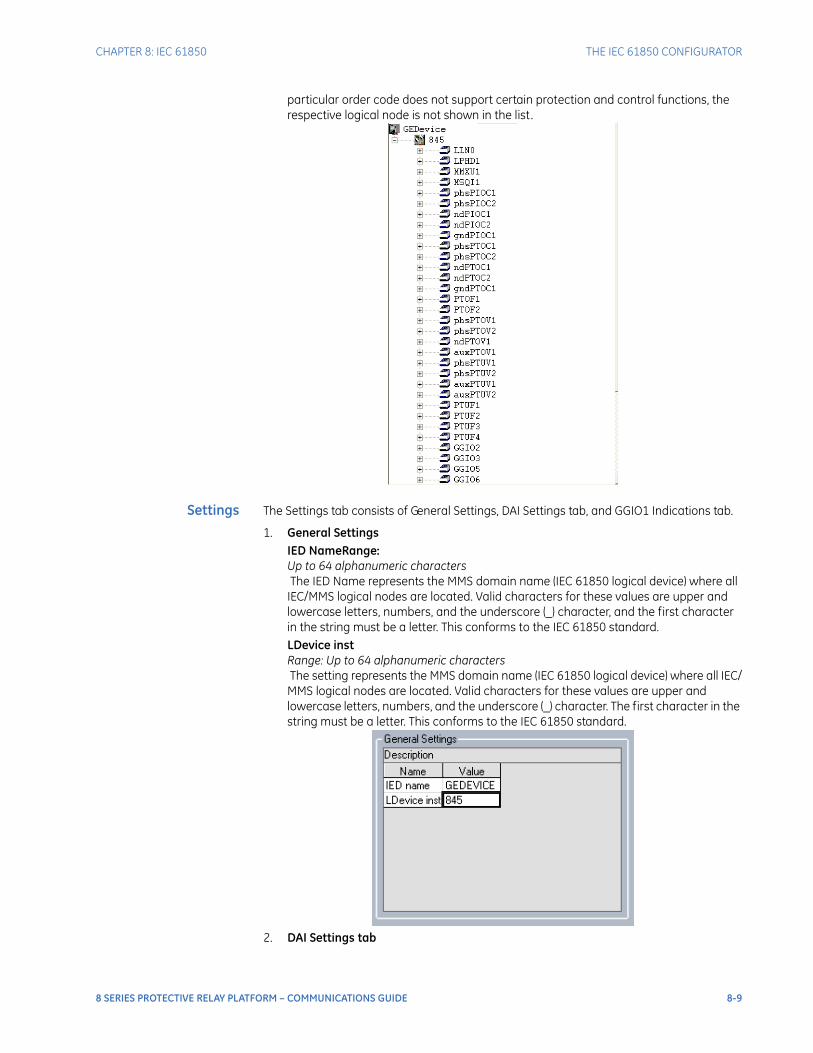
CHAPTER 8: IEC 61850 THE IEC 61850 CONFIGURATOR
particular order code does not support certain protection and control functions, the respective logical node is not shown in the list.
Settings The Settings tab consists of General Settings, DAI Settings tab, and GGIO1 Indications tab.
1. General SettingsIED NameRange: Up to 64 alphanumeric characters The IED Name represents the MMS domain name (IEC 61850 logical device) where all IEC/MMS logical nodes are located. Valid characters for these values are upper and lowercase letters, numbers, and the underscore (_) character, and the first character in the string must be a letter. This conforms to the IEC 61850 standard.LDevice inst Range: Up to 64 alphanumeric characters The setting represents the MMS domain name (IEC 61850 logical device) where all IEC/MMS logical nodes are located. Valid characters for these values are upper and lowercase letters, numbers, and the underscore (_) character. The first character in the string must be a letter. This conforms to the IEC 61850 standard.
2. DAI Settings tab
8 SERIES PROTECTIVE RELAY PLATFORM – COMMUNICATIONS GUIDE 8-9
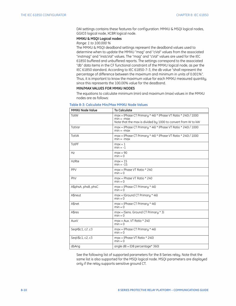
THE IEC 61850 CONFIGURATOR CHAPTER 8: IEC 61850
DAI settings contains these features for configuration: MMXU & MSQI logical nodes, GGIO3 logical node, XCBR logical node.MMXU & MSQI Logical nodes Range: 1 to 100.000 % The MMXU & MSQI deadband settings represent the deadband values used to determine when to update the MMXU “mag” and “cVal” values from the associated “instmag” and “instcVal” values. The “mag” and “cVal” values are used for the IEC 61850 buffered and unbuffered reports. The settings correspond to the associated “db” data items in the CF functional constraint of the MMXU logical node, as per the IEC 61850 standard. According to IEC 61850-7-3, the db value “shall represent the percentage of difference between the maximum and minimum in units of 0.001%”. Thus, it is important to know the maximum value for each MMXU measured quantity, since this represents the 100.00% value for the deadband.MIN/MAX VALUES FOR MMXU NODESThe equations to calculate minimum (min) and maximum (max) values in the MMXU nodes are as follows:
Table 8-3: Calculate Min/Max MMXU Node Values
See the following list of supported parameters for the 8 Series relay. Note that the same list is also supported for the MSQI logical node. MSQI parameters are displayed only if the relay supports sensitive ground CT.
MMXU Node Value To Calculate
TotW max = (Phase CT Primary * 46) * (Phase VT Ratio * 240) / 1000min = -maxNote that the max is divided by 1000 to convert from W to kW
TotVar max = (Phase CT Primary * 46) * (Phase VT Ratio * 240) / 1000min = -max
TotVA max = (Phase CT Primary * 46) * (Phase VT Ratio * 240) / 1000min = -max
TotPF max = 1min = -1
Hz max = 90min = 0
HzRte max = 15min = -15
PPV max = Phase VT Ratio * 240min = 0
PhV max = Phase VT Ratio * 240min = 0
A$phsA, phsB, phsC max = (Phase CT Primary * 46)min = 0
A$neut max = (Ground CT Primary * 46)min = 0
A$net max = (Phase CT Primary * 46)min = 0
A$res max = (Sens. Ground CT Primary * 3)min = 0
AuxV max = Aux. VT Ratio * 240min = 0
SeqA$c1, c2 ,c3 max = (Phase CT Primary * 46)min = 0
SeqV$c1, c2, c3 max = (Phase VT Ratio * 240)min = 0
dbAng angle dB = (DB percentage* 360)
8-10 8 SERIES PROTECTIVE RELAY PLATFORM – COMMUNICATIONS GUIDE
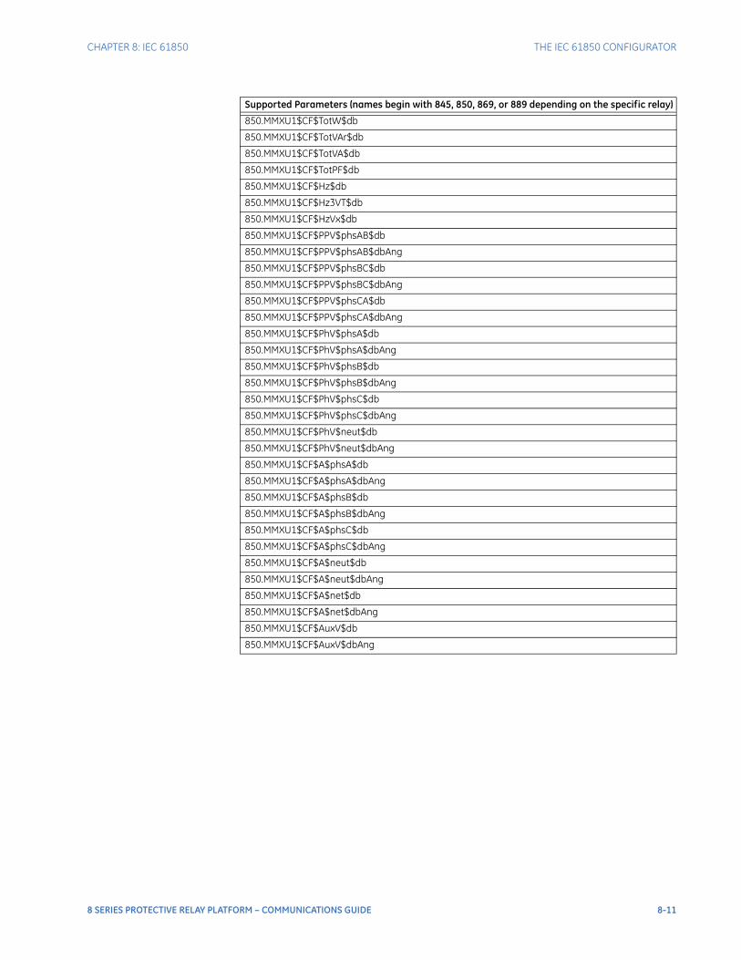
CHAPTER 8: IEC 61850 THE IEC 61850 CONFIGURATOR
Supported Parameters (names begin with 845, 850, 869, or 889 depending on the specific relay)
850.MMXU1$CF$TotW$db
850.MMXU1$CF$TotVAr$db
850.MMXU1$CF$TotVA$db
850.MMXU1$CF$TotPF$db
850.MMXU1$CF$Hz$db
850.MMXU1$CF$Hz3VT$db
850.MMXU1$CF$HzVx$db
850.MMXU1$CF$PPV$phsAB$db
850.MMXU1$CF$PPV$phsAB$dbAng
850.MMXU1$CF$PPV$phsBC$db
850.MMXU1$CF$PPV$phsBC$dbAng
850.MMXU1$CF$PPV$phsCA$db
850.MMXU1$CF$PPV$phsCA$dbAng
850.MMXU1$CF$PhV$phsA$db
850.MMXU1$CF$PhV$phsA$dbAng
850.MMXU1$CF$PhV$phsB$db
850.MMXU1$CF$PhV$phsB$dbAng
850.MMXU1$CF$PhV$phsC$db
850.MMXU1$CF$PhV$phsC$dbAng
850.MMXU1$CF$PhV$neut$db
850.MMXU1$CF$PhV$neut$dbAng
850.MMXU1$CF$A$phsA$db
850.MMXU1$CF$A$phsA$dbAng
850.MMXU1$CF$A$phsB$db
850.MMXU1$CF$A$phsB$dbAng
850.MMXU1$CF$A$phsC$db
850.MMXU1$CF$A$phsC$dbAng
850.MMXU1$CF$A$neut$db
850.MMXU1$CF$A$neut$dbAng
850.MMXU1$CF$A$net$db
850.MMXU1$CF$A$net$dbAng
850.MMXU1$CF$AuxV$db
850.MMXU1$CF$AuxV$dbAng
8 SERIES PROTECTIVE RELAY PLATFORM – COMMUNICATIONS GUIDE 8-11
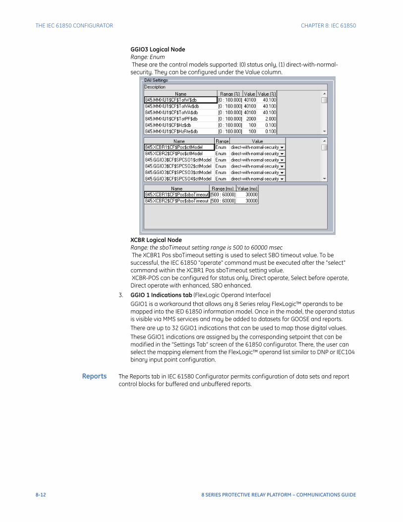
THE IEC 61850 CONFIGURATOR CHAPTER 8: IEC 61850
GGIO3 Logical Node Range: Enum These are the control models supported: (0) status only, (1) direct-with-normal-security. They can be configured under the Value column.
XCBR Logical Node Range: the sboTimeout setting range is 500 to 60000 msec The XCBR1 Pos sboTimeout setting is used to select SBO timeout value. To be successful, the IEC 61850 "operate" command must be executed after the "select" command within the XCBR1 Pos sboTimeout setting value. XCBR-POS can be configured for status only, Direct operate, Select before operate, Direct operate with enhanced, SBO enhanced.
3. GGIO 1 Indications tab (FlexLogic Operand Interface)GGIO1 is a workaround that allows any 8 Series relay FlexLogic™ operands to be mapped into the IED 61850 information model. Once in the model, the operand status is visible via MMS services and may be added to datasets for GOOSE and reports.There are up to 32 GGIO1 indications that can be used to map those digital values.These GGIO1 indications are assigned by the corresponding setpoint that can be modified in the “Settings Tab” screen of the 61850 configurator. There, the user can select the mapping element from the FlexLogic™ operand list similar to DNP or IEC104 binary input point configuration.
Reports The Reports tab in IEC 61580 Configurator permits configuration of data sets and report control blocks for buffered and unbuffered reports.
8-12 8 SERIES PROTECTIVE RELAY PLATFORM – COMMUNICATIONS GUIDE
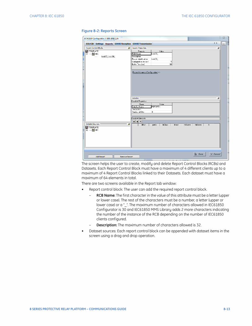
CHAPTER 8: IEC 61850 THE IEC 61850 CONFIGURATOR
Figure 8-2: Reports Screen
The screen helps the user to create, modify and delete Report Control Blocks (RCBs) and Datasets. Each Report Control Block must have a maximum of 4 different clients up to a maximum of 4 Report Control Blocks linked to their Datasets. Each dataset must have a maximum of 64 elements in total.There are two screens available in the Report tab window:
• Report control block: The user can add the required report control block.
– RCB Name: The first character in the value of this attribute must be a letter (upper or lower case). The rest of the characters must be a number, a letter (upper or lower case) or a “_”. The maximum number of characters allowed in IEC61850 Configurator is 30 and IEC61850 MMS Library adds 2 more characters indicating the number of the instance of the RCB depending on the number of IEC61850 clients configured.
– Description: The maximum number of characters allowed is 32.
• Dataset sources: Each report control block can be appended with dataset items in the screen using a drag and drop operation.
8 SERIES PROTECTIVE RELAY PLATFORM – COMMUNICATIONS GUIDE 8-13
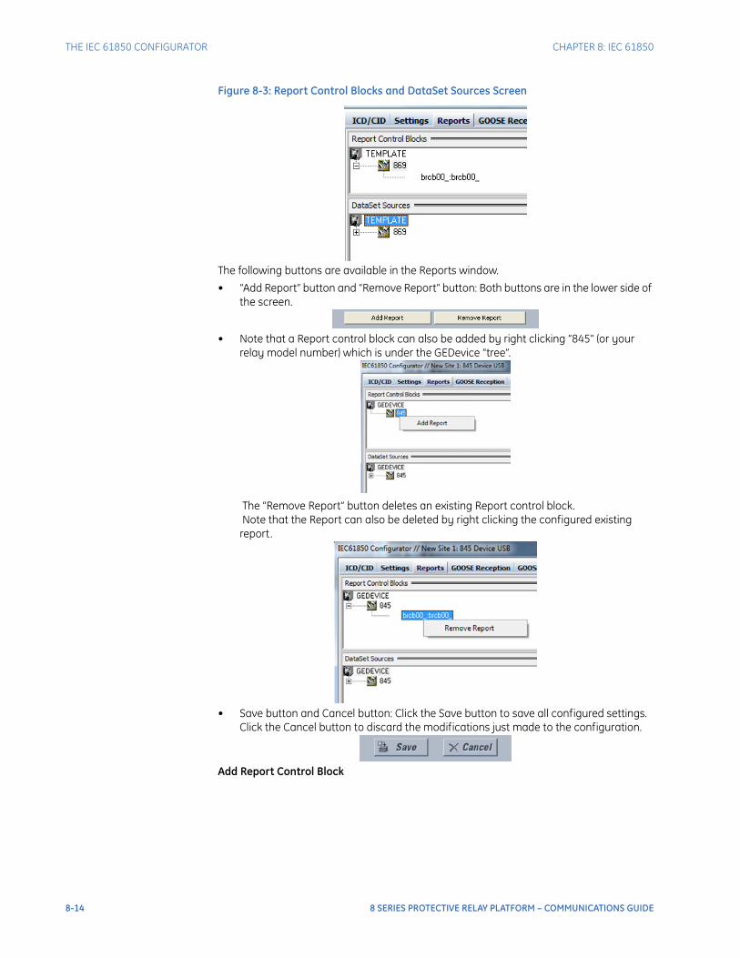
THE IEC 61850 CONFIGURATOR CHAPTER 8: IEC 61850
Figure 8-3: Report Control Blocks and DataSet Sources Screen
The following buttons are available in the Reports window.
• “Add Report” button and “Remove Report” button: Both buttons are in the lower side of the screen.
• Note that a Report control block can also be added by right clicking “845” (or your relay model number) which is under the GEDevice “tree”.
The “Remove Report” button deletes an existing Report control block. Note that the Report can also be deleted by right clicking the configured existing report.
• Save button and Cancel button: Click the Save button to save all configured settings. Click the Cancel button to discard the modifications just made to the configuration.
Add Report Control Block
8-14 8 SERIES PROTECTIVE RELAY PLATFORM – COMMUNICATIONS GUIDE
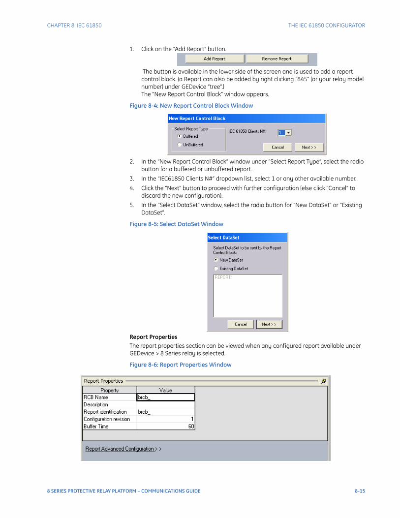
CHAPTER 8: IEC 61850 THE IEC 61850 CONFIGURATOR
1. Click on the “Add Report” button.
The button is available in the lower side of the screen and is used to add a report control block. (a Report can also be added by right clicking “845” (or your relay model number) under GEDevice “tree”.) The “New Report Control Block” window appears.
Figure 8-4: New Report Control Block Window
2. In the “New Report Control Block” window under “Select Report Type”, select the radio button for a buffered or unbuffered report.
3. In the “IEC61850 Clients N#” dropdown list, select 1 or any other available number.
4. Click the “Next” button to proceed with further configuration (else click “Cancel” to discard the new configuration).
5. In the “Select DataSet” window, select the radio button for “New DataSet” or “Existing DataSet”.
Figure 8-5: Select DataSet Window
Report PropertiesThe report properties section can be viewed when any configured report available under GEDevice > 8 Series relay is selected.
Figure 8-6: Report Properties Window
8 SERIES PROTECTIVE RELAY PLATFORM – COMMUNICATIONS GUIDE 8-15
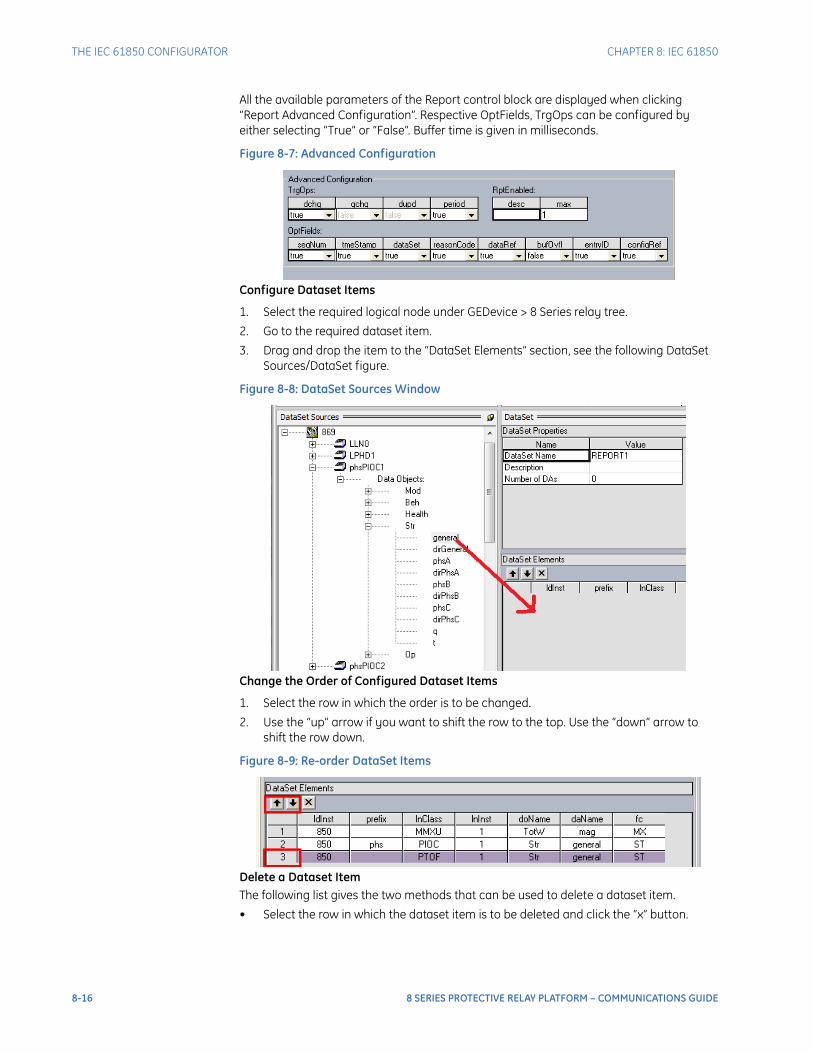
THE IEC 61850 CONFIGURATOR CHAPTER 8: IEC 61850
All the available parameters of the Report control block are displayed when clicking “Report Advanced Configuration”. Respective OptFields, TrgOps can be configured by either selecting “True” or “False”. Buffer time is given in milliseconds.
Figure 8-7: Advanced Configuration
Configure Dataset Items
1. Select the required logical node under GEDevice > 8 Series relay tree.
2. Go to the required dataset item.
3. Drag and drop the item to the “DataSet Elements” section, see the following DataSet Sources/DataSet figure.
Figure 8-8: DataSet Sources Window
Change the Order of Configured Dataset Items
1. Select the row in which the order is to be changed.
2. Use the “up” arrow if you want to shift the row to the top. Use the “down” arrow to shift the row down.
Figure 8-9: Re-order DataSet Items
Delete a Dataset ItemThe following list gives the two methods that can be used to delete a dataset item.
• Select the row in which the dataset item is to be deleted and click the “x” button.
8-16 8 SERIES PROTECTIVE RELAY PLATFORM – COMMUNICATIONS GUIDE
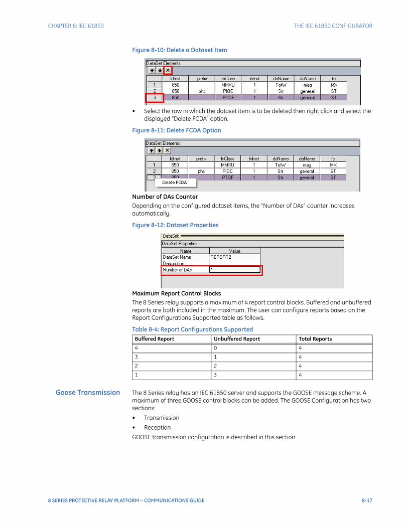
CHAPTER 8: IEC 61850 THE IEC 61850 CONFIGURATOR
Figure 8-10: Delete a Dataset Item
• Select the row in which the dataset item is to be deleted then right click and select the displayed “Delete FCDA” option.
Figure 8-11: Delete FCDA Option
Number of DAs CounterDepending on the configured dataset items, the “Number of DAs” counter increases automatically.
Figure 8-12: Dataset Properties
Maximum Report Control BlocksThe 8 Series relay supports a maximum of 4 report control blocks. Buffered and unbuffered reports are both included in the maximum. The user can configure reports based on the Report Configurations Supported table as follows.
Table 8-4: Report Configurations Supported
Goose Transmission The 8 Series relay has an IEC 61850 server and supports the GOOSE message scheme. A maximum of three GOOSE control blocks can be added. The GOOSE Configuration has two sections:
• Transmission
• Reception
GOOSE transmission configuration is described in this section.
Buffered Report Unbuffered Report Total Reports
4 0 4
3 1 4
2 2 4
1 3 4
8 SERIES PROTECTIVE RELAY PLATFORM – COMMUNICATIONS GUIDE 8-17
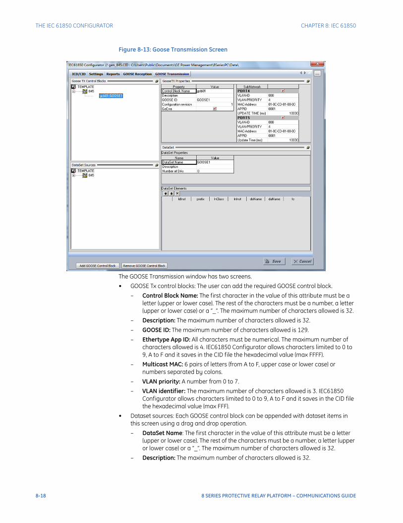
THE IEC 61850 CONFIGURATOR CHAPTER 8: IEC 61850
Figure 8-13: Goose Transmission Screen
The GOOSE Transmission window has two screens.
• GOOSE Tx control blocks: The user can add the required GOOSE control block.
– Control Block Name: The first character in the value of this attribute must be a letter (upper or lower case). The rest of the characters must be a number, a letter (upper or lower case) or a “_”. The maximum number of characters allowed is 32.
– Description: The maximum number of characters allowed is 32.
– GOOSE ID: The maximum number of characters allowed is 129.
– Ethertype App ID: All characters must be numerical. The maximum number of characters allowed is 4. IEC61850 Configurator allows characters limited to 0 to 9, A to F and it saves in the CID file the hexadecimal value (max FFFF).
– Multicast MAC: 6 pairs of letters (from A to F, upper case or lower case) or numbers separated by colons.
– VLAN priority: A number from 0 to 7.
– VLAN identifier: The maximum number of characters allowed is 3. IEC61850 Configurator allows characters limited to 0 to 9, A to F and it saves in the CID file the hexadecimal value (max FFF).
• Dataset sources: Each GOOSE control block can be appended with dataset items in this screen using a drag and drop operation.
– DataSet Name: The first character in the value of this attribute must be a letter (upper or lower case). The rest of the characters must be a number, a letter (upper or lower case) or a “_”. The maximum number of characters allowed is 32.
– Description: The maximum number of characters allowed is 32.
8-18 8 SERIES PROTECTIVE RELAY PLATFORM – COMMUNICATIONS GUIDE
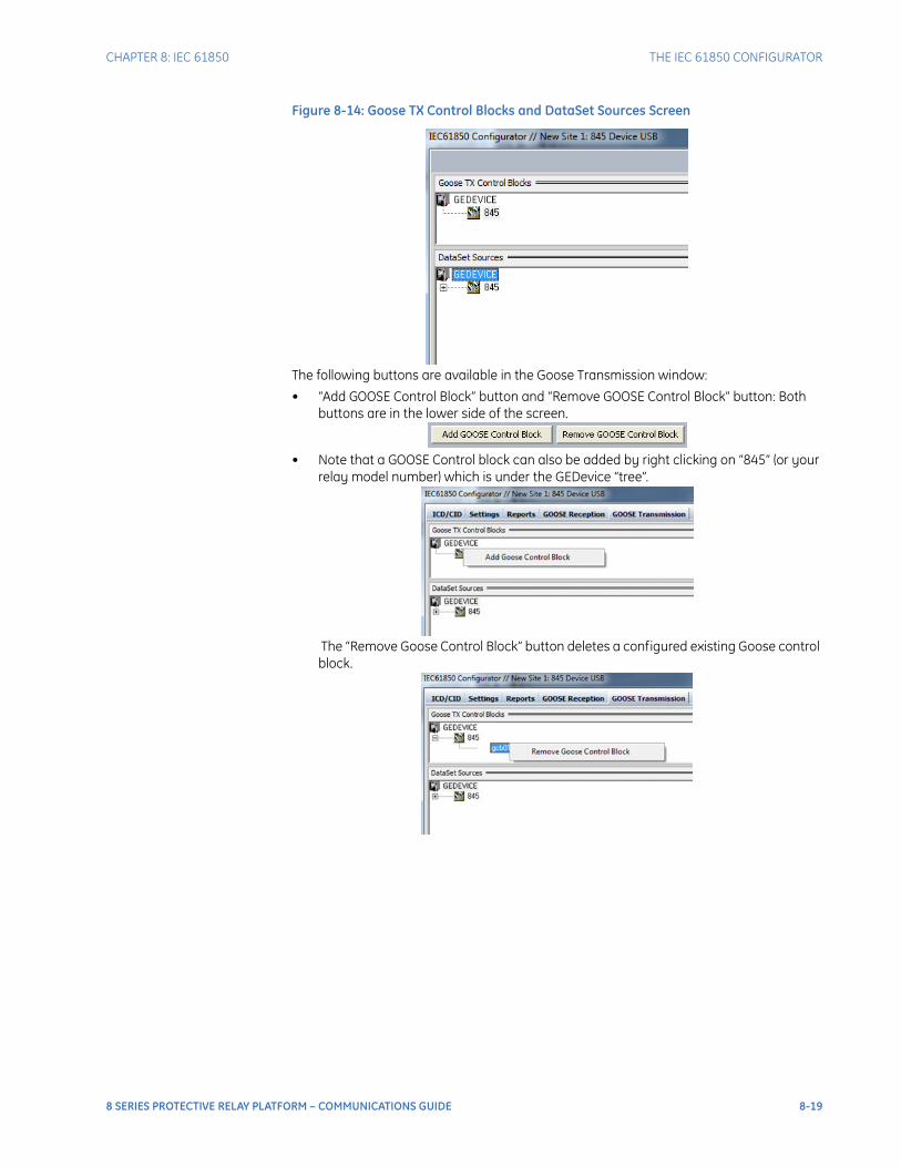
CHAPTER 8: IEC 61850 THE IEC 61850 CONFIGURATOR
Figure 8-14: Goose TX Control Blocks and DataSet Sources Screen
The following buttons are available in the Goose Transmission window:
• “Add GOOSE Control Block” button and “Remove GOOSE Control Block” button: Both buttons are in the lower side of the screen.
• Note that a GOOSE Control block can also be added by right clicking on “845” (or your relay model number) which is under the GEDevice “tree”.
The “Remove Goose Control Block” button deletes a configured existing Goose control block.
8 SERIES PROTECTIVE RELAY PLATFORM – COMMUNICATIONS GUIDE 8-19
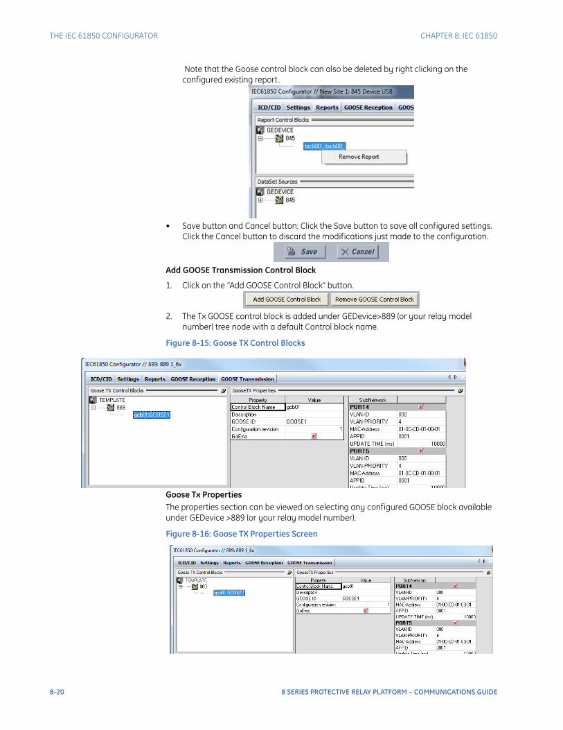
THE IEC 61850 CONFIGURATOR CHAPTER 8: IEC 61850
Note that the Goose control block can also be deleted by right clicking on the configured existing report.
• Save button and Cancel button: Click the Save button to save all configured settings. Click the Cancel button to discard the modifications just made to the configuration.
Add GOOSE Transmission Control Block
1. Click on the “Add GOOSE Control Block” button.
2. The Tx GOOSE control block is added under GEDevice>889 (or your relay model number) tree node with a default Control block name.
Figure 8-15: Goose TX Control Blocks
Goose Tx PropertiesThe properties section can be viewed on selecting any configured GOOSE block available under GEDevice >889 (or your relay model number).
Figure 8-16: Goose TX Properties Screen
8-20 8 SERIES PROTECTIVE RELAY PLATFORM – COMMUNICATIONS GUIDE
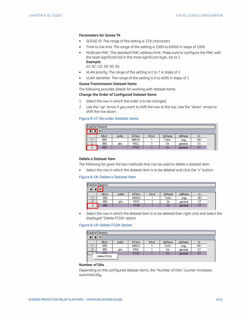
CHAPTER 8: IEC 61850 THE IEC 61850 CONFIGURATOR
Parameters for Goose TX
• GOOSE ID: The range of the setting is 129-characters
• Time to live (ms): The range of the setting is 1000 to 60000 in steps of 1000
• Multicast MAC: The standard MAC address limit. Make sure to configure the MAC with the least significant bit in the most significant byte, set to 1. Example: 01: 0C: CD: 00: 00: 04
• VLAN priority: The range of the setting is 0 to 7 in steps of 1
• VLAN identifier: The range of the setting is 0 to 4095 in steps of 1
Goose Transmission Dataset ItemsThe following provides details for working with dataset items.Change the Order of Configured Dataset Items
1. Select the row in which the order is to be changed.
2. Use the “up” arrow if you want to shift the row to the top. Use the “down” arrow to shift the row down.
Figure 8-17: Re-order DataSet Items
Delete a Dataset ItemThe following list gives the two methods that can be used to delete a dataset item.
• Select the row in which the dataset item is to be deleted and click the “x” button.
Figure 8-18: Delete a Dataset Item
• Select the row in which the dataset item is to be deleted then right click and select the displayed “Delete FCDA” option.
Figure 8-19: Delete FCDA Option
Number of DAsDepending on the configured dataset items, the “Number of DAs” counter increases automatically.
8 SERIES PROTECTIVE RELAY PLATFORM – COMMUNICATIONS GUIDE 8-21
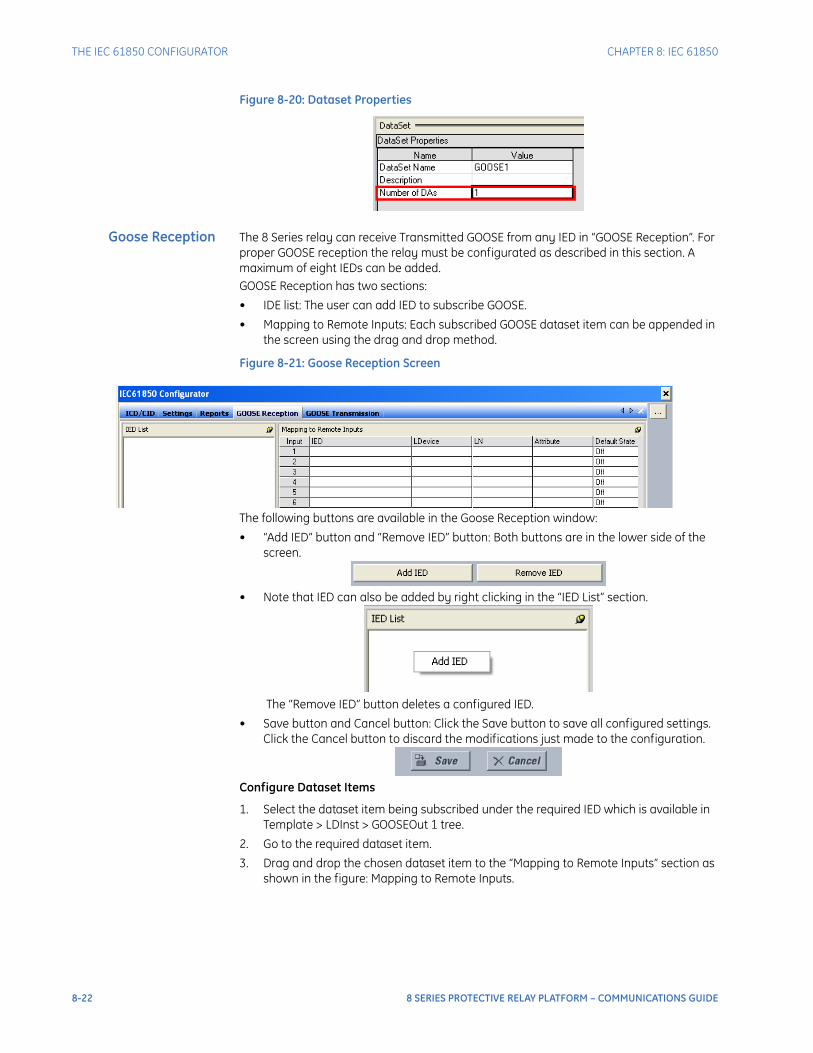
THE IEC 61850 CONFIGURATOR CHAPTER 8: IEC 61850
Figure 8-20: Dataset Properties
Goose Reception The 8 Series relay can receive Transmitted GOOSE from any IED in “GOOSE Reception”. For proper GOOSE reception the relay must be configurated as described in this section. A maximum of eight IEDs can be added.GOOSE Reception has two sections:
• IDE list: The user can add IED to subscribe GOOSE.
• Mapping to Remote Inputs: Each subscribed GOOSE dataset item can be appended in the screen using the drag and drop method.
Figure 8-21: Goose Reception Screen
The following buttons are available in the Goose Reception window:
• “Add IED” button and “Remove IED” button: Both buttons are in the lower side of the screen.
• Note that IED can also be added by right clicking in the “IED List” section.
The “Remove IED” button deletes a configured IED.
• Save button and Cancel button: Click the Save button to save all configured settings. Click the Cancel button to discard the modifications just made to the configuration.
Configure Dataset Items
1. Select the dataset item being subscribed under the required IED which is available in Template > LDInst > GOOSEOut 1 tree.
2. Go to the required dataset item.
3. Drag and drop the chosen dataset item to the “Mapping to Remote Inputs” section as shown in the figure: Mapping to Remote Inputs.
8-22 8 SERIES PROTECTIVE RELAY PLATFORM – COMMUNICATIONS GUIDE
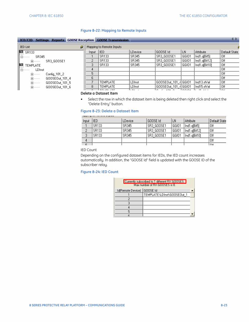
CHAPTER 8: IEC 61850 THE IEC 61850 CONFIGURATOR
Figure 8-22: Mapping to Remote Inputs
Delete a Dataset Item
• Select the row in which the dataset item is being deleted then right click and select the “Delete Entry” button.
Figure 8-23: Delete a Dataset Item
IED CountDepending on the configured dataset items for IEDs, the IED count increases automatically. In addition, the ”GOOSE Id” field is updated with the GOOSE ID of the subscriber relay.
Figure 8-24: IED Count
8 SERIES PROTECTIVE RELAY PLATFORM – COMMUNICATIONS GUIDE 8-23

THE IEC 61850 CONFIGURATOR CHAPTER 8: IEC 61850
8-24 8 SERIES PROTECTIVE RELAY PLATFORM – COMMUNICATIONS GUIDE
8 Series Protective Relay Platform
Chapter 9: File Transfer Protocols
GEGrid Solutions
File Transfer Protocols
The base offering of 8 Series relay supports Trivial File Transfer Protocol (TFTP). The default port 69 is always used. No configuration setting is available. When the communications module is present, SSH File Transfer Protocol (SFTP) is also available. The default TCP port 22 for SSH is used for SFTP as well.
8 SERIES PROTECTIVE RELAY PLATFORM – COMMUNICATIONS GUIDE 9-1

CHAPTER 9: FILE TRANSFER PROTOCOLS
9-2 8 SERIES PROTECTIVE RELAY PLATFORM – COMMUNICATIONS GUIDE
8 Series Protective Relay Platform
Chapter 10: Modbus Protocol
GEGrid Solutions
Modbus Protocol
All Ethernet ports and serial communication ports support the Modbus protocol. The only exception is if the serial port has been configured for DNP or IEC 60870-5-103 operation (see descriptions below). This allows the EnerVista 8 Series Setup software (which is a Modbus master application) to communicate to the 8 Series relay. The 8 Series relay implements a subset of the Modicon Modbus RTU serial communication standard. The Modbus protocol is hardware-independent. That is, the physical layer can be any of a variety of standard hardware configurations. This includes USB, RS485, fiber optics, etc. Modbus is a single master / multiple slave type of protocol suitable for a multi-drop configuration. The 8 Series relay is always a Modbus slave with a valid slave address range 1 to 254.DATA FRAME FORMAT AND DATA RATEOne data frame of an asynchronous transmission to or from an 8 Series relay typically consists of 1 start bit, 8 data bits, and 1 stop bit. This produces a 10-bit data frame. This is important for transmission through modems at high bit rates. Modbus protocol can be implemented at any standard communication speed. The 8 Series relay supports operation at 9600, 19200, 38400, 57600, and 115200 bps baud rate. The USB interface supports ModBus TCP/IP.
FUNCTION CODE SUPPORTEDThe following functions are supported by the 8 Series relay:
• FUNCTION CODE 03H - Read Setpoints
• FUNCTION CODE 04H - Read Actual Values
• FUNCTION CODE 05H - Execute Operation
• FUNCTION CODE 06H - Store Single Setpoint
• FUNCTION CODE 07H - Read Device Status
• FUNCTION CODE 08H - Loopback Test
• FUNCTION CODE 10H - Store Multiple Setpoints
• FUNCTION CODE 42H - Group Settings Read
• FUNCTION CODE 43H - Group Settings Write
When a ModBus master such as the EnerVista 8 Series Setup software communicates to the 8 Series relay over Ethernet, the 8 Series relay slave address, TCP port number and the 8 Series relay IP address for the associated port must be configured and are also configured within the Master for this device. The default ModBus TCP port number is 502.
8 SERIES PROTECTIVE RELAY PLATFORM – COMMUNICATIONS GUIDE 10-1
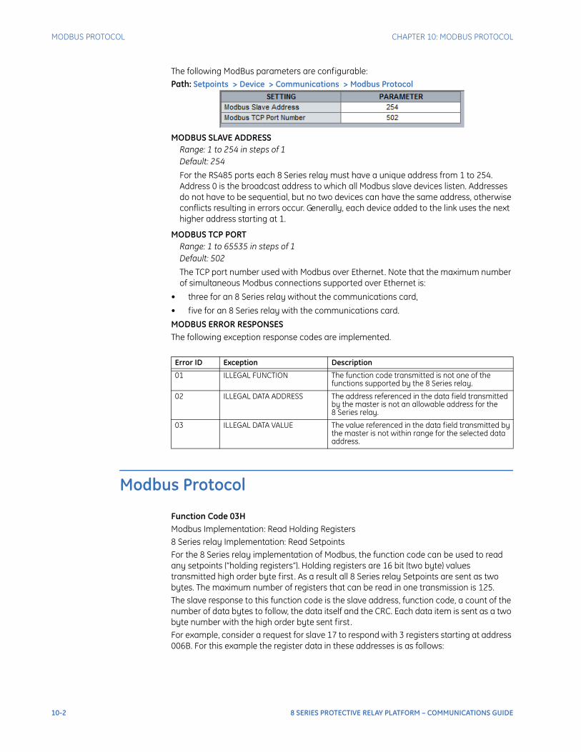
MODBUS PROTOCOL CHAPTER 10: MODBUS PROTOCOL
The following ModBus parameters are configurable:Path: Setpoints > Device > Communications > Modbus Protocol
MODBUS SLAVE ADDRESSRange: 1 to 254 in steps of 1Default: 254
For the RS485 ports each 8 Series relay must have a unique address from 1 to 254. Address 0 is the broadcast address to which all Modbus slave devices listen. Addresses do not have to be sequential, but no two devices can have the same address, otherwise conflicts resulting in errors occur. Generally, each device added to the link uses the next higher address starting at 1.
MODBUS TCP PORTRange: 1 to 65535 in steps of 1Default: 502
The TCP port number used with Modbus over Ethernet. Note that the maximum number of simultaneous Modbus connections supported over Ethernet is:
• three for an 8 Series relay without the communications card,
• five for an 8 Series relay with the communications card.
MODBUS ERROR RESPONSESThe following exception response codes are implemented.
Modbus Protocol
Function Code 03HModbus Implementation: Read Holding Registers8 Series relay Implementation: Read SetpointsFor the 8 Series relay implementation of Modbus, the function code can be used to read any setpoints (“holding registers”). Holding registers are 16 bit (two byte) values transmitted high order byte first. As a result all 8 Series relay Setpoints are sent as two bytes. The maximum number of registers that can be read in one transmission is 125.The slave response to this function code is the slave address, function code, a count of the number of data bytes to follow, the data itself and the CRC. Each data item is sent as a two byte number with the high order byte sent first.For example, consider a request for slave 17 to respond with 3 registers starting at address 006B. For this example the register data in these addresses is as follows:
Error ID Exception Description
01 ILLEGAL FUNCTION The function code transmitted is not one of the functions supported by the 8 Series relay.
02 ILLEGAL DATA ADDRESS The address referenced in the data field transmitted by the master is not an allowable address for the 8 Series relay.
03 ILLEGAL DATA VALUE The value referenced in the data field transmitted by the master is not within range for the selected data address.
10-2 8 SERIES PROTECTIVE RELAY PLATFORM – COMMUNICATIONS GUIDE
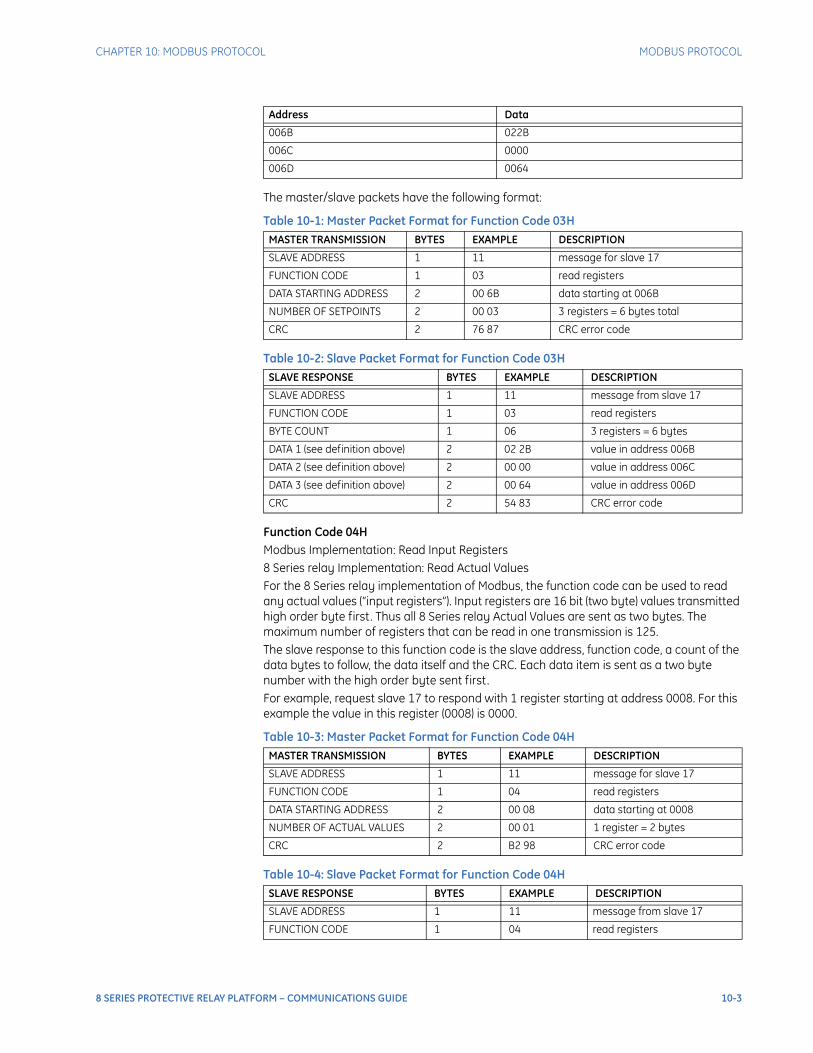
CHAPTER 10: MODBUS PROTOCOL MODBUS PROTOCOL
The master/slave packets have the following format:
Table 10-1: Master Packet Format for Function Code 03H
Table 10-2: Slave Packet Format for Function Code 03H
Function Code 04HModbus Implementation: Read Input Registers8 Series relay Implementation: Read Actual ValuesFor the 8 Series relay implementation of Modbus, the function code can be used to read any actual values (“input registers”). Input registers are 16 bit (two byte) values transmitted high order byte first. Thus all 8 Series relay Actual Values are sent as two bytes. The maximum number of registers that can be read in one transmission is 125.The slave response to this function code is the slave address, function code, a count of the data bytes to follow, the data itself and the CRC. Each data item is sent as a two byte number with the high order byte sent first.For example, request slave 17 to respond with 1 register starting at address 0008. For this example the value in this register (0008) is 0000.
Table 10-3: Master Packet Format for Function Code 04H
Table 10-4: Slave Packet Format for Function Code 04H
Address Data
006B 022B
006C 0000
006D 0064
MASTER TRANSMISSION BYTES EXAMPLE DESCRIPTION
SLAVE ADDRESS 1 11 message for slave 17
FUNCTION CODE 1 03 read registers
DATA STARTING ADDRESS 2 00 6B data starting at 006B
NUMBER OF SETPOINTS 2 00 03 3 registers = 6 bytes total
CRC 2 76 87 CRC error code
SLAVE RESPONSE BYTES EXAMPLE DESCRIPTION
SLAVE ADDRESS 1 11 message from slave 17
FUNCTION CODE 1 03 read registers
BYTE COUNT 1 06 3 registers = 6 bytes
DATA 1 (see definition above) 2 02 2B value in address 006B
DATA 2 (see definition above) 2 00 00 value in address 006C
DATA 3 (see definition above) 2 00 64 value in address 006D
CRC 2 54 83 CRC error code
MASTER TRANSMISSION BYTES EXAMPLE DESCRIPTION
SLAVE ADDRESS 1 11 message for slave 17
FUNCTION CODE 1 04 read registers
DATA STARTING ADDRESS 2 00 08 data starting at 0008
NUMBER OF ACTUAL VALUES 2 00 01 1 register = 2 bytes
CRC 2 B2 98 CRC error code
SLAVE RESPONSE BYTES EXAMPLE DESCRIPTION
SLAVE ADDRESS 1 11 message from slave 17
FUNCTION CODE 1 04 read registers
8 SERIES PROTECTIVE RELAY PLATFORM – COMMUNICATIONS GUIDE 10-3
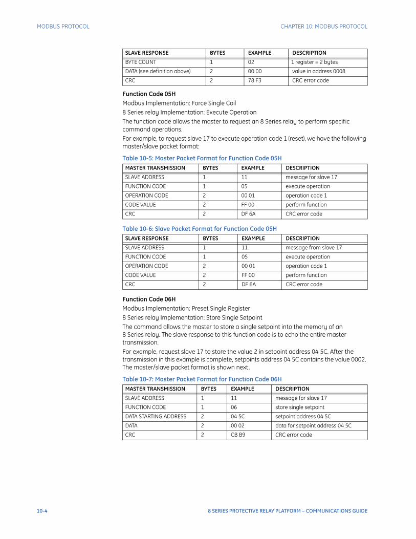
MODBUS PROTOCOL CHAPTER 10: MODBUS PROTOCOL
Function Code 05HModbus Implementation: Force Single Coil8 Series relay Implementation: Execute OperationThe function code allows the master to request an 8 Series relay to perform specific command operations.For example, to request slave 17 to execute operation code 1 (reset), we have the following master/slave packet format:
Table 10-5: Master Packet Format for Function Code 05H
Table 10-6: Slave Packet Format for Function Code 05H
Function Code 06HModbus Implementation: Preset Single Register8 Series relay Implementation: Store Single SetpointThe command allows the master to store a single setpoint into the memory of an 8 Series relay. The slave response to this function code is to echo the entire master transmission.For example, request slave 17 to store the value 2 in setpoint address 04 5C. After the transmission in this example is complete, setpoints address 04 5C contains the value 0002. The master/slave packet format is shown next.
Table 10-7: Master Packet Format for Function Code 06H
BYTE COUNT 1 02 1 register = 2 bytes
DATA (see definition above) 2 00 00 value in address 0008
CRC 2 78 F3 CRC error code
MASTER TRANSMISSION BYTES EXAMPLE DESCRIPTION
SLAVE ADDRESS 1 11 message for slave 17
FUNCTION CODE 1 05 execute operation
OPERATION CODE 2 00 01 operation code 1
CODE VALUE 2 FF 00 perform function
CRC 2 DF 6A CRC error code
SLAVE RESPONSE BYTES EXAMPLE DESCRIPTION
SLAVE ADDRESS 1 11 message from slave 17
FUNCTION CODE 1 05 execute operation
OPERATION CODE 2 00 01 operation code 1
CODE VALUE 2 FF 00 perform function
CRC 2 DF 6A CRC error code
MASTER TRANSMISSION BYTES EXAMPLE DESCRIPTION
SLAVE ADDRESS 1 11 message for slave 17
FUNCTION CODE 1 06 store single setpoint
DATA STARTING ADDRESS 2 04 5C setpoint address 04 5C
DATA 2 00 02 data for setpoint address 04 5C
CRC 2 CB B9 CRC error code
SLAVE RESPONSE BYTES EXAMPLE DESCRIPTION
10-4 8 SERIES PROTECTIVE RELAY PLATFORM – COMMUNICATIONS GUIDE
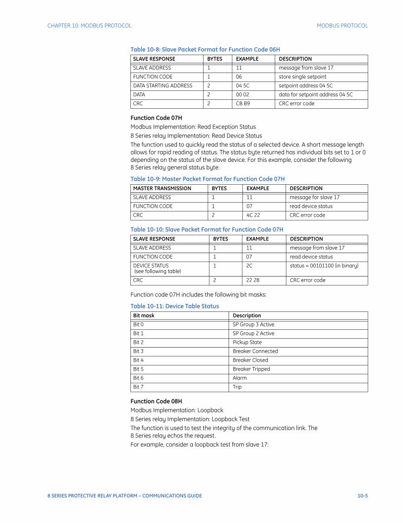
CHAPTER 10: MODBUS PROTOCOL MODBUS PROTOCOL
Table 10-8: Slave Packet Format for Function Code 06H
Function Code 07HModbus Implementation: Read Exception Status8 Series relay Implementation: Read Device StatusThe function used to quickly read the status of a selected device. A short message length allows for rapid reading of status. The status byte returned has individual bits set to 1 or 0 depending on the status of the slave device. For this example, consider the following 8 Series relay general status byte:
Table 10-9: Master Packet Format for Function Code 07H
Table 10-10: Slave Packet Format for Function Code 07H
Function code 07H includes the following bit masks:
Table 10-11: Device Table Status
Function Code 08HModbus Implementation: Loopback8 Series relay Implementation: Loopback TestThe function is used to test the integrity of the communication link. The 8 Series relay echos the request.For example, consider a loopback test from slave 17:
SLAVE RESPONSE BYTES EXAMPLE DESCRIPTION
SLAVE ADDRESS 1 11 message from slave 17
FUNCTION CODE 1 06 store single setpoint
DATA STARTING ADDRESS 2 04 5C setpoint address 04 5C
DATA 2 00 02 data for setpoint address 04 5C
CRC 2 CB B9 CRC error code
MASTER TRANSMISSION BYTES EXAMPLE DESCRIPTION
SLAVE ADDRESS 1 11 message for slave 17
FUNCTION CODE 1 07 read device status
CRC 2 4C 22 CRC error code
SLAVE RESPONSE BYTES EXAMPLE DESCRIPTION
SLAVE ADDRESS 1 11 message from slave 17
FUNCTION CODE 1 07 read device status
DEVICE STATUS (see following table)
1 2C status = 00101100 (in binary)
CRC 2 22 28 CRC error code
Bit mask Description
Bit 0 SP Group 3 Active
Bit 1 SP Group 2 Active
Bit 2 Pickup State
Bit 3 Breaker Connected
Bit 4 Breaker Closed
Bit 5 Breaker Tripped
Bit 6 Alarm
Bit 7 Trip
8 SERIES PROTECTIVE RELAY PLATFORM – COMMUNICATIONS GUIDE 10-5
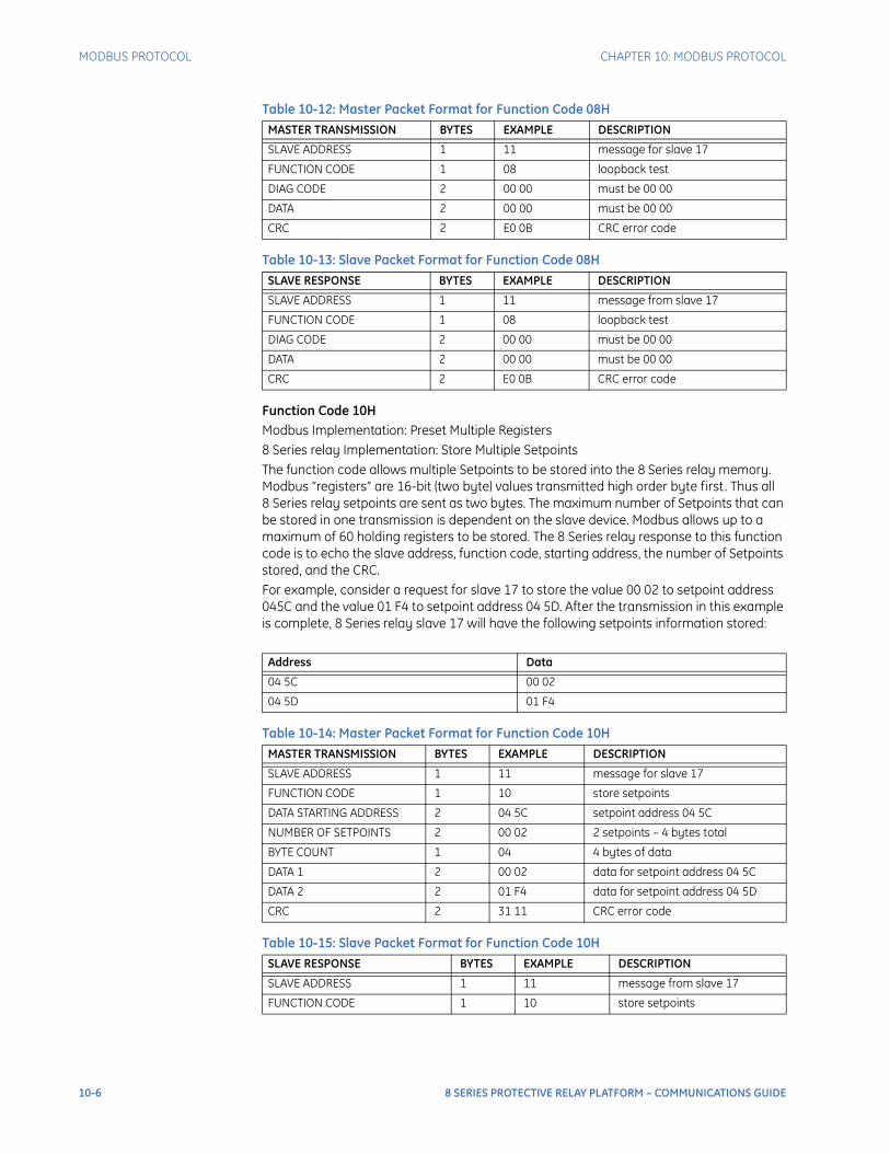
MODBUS PROTOCOL CHAPTER 10: MODBUS PROTOCOL
Table 10-12: Master Packet Format for Function Code 08H
Table 10-13: Slave Packet Format for Function Code 08H
Function Code 10HModbus Implementation: Preset Multiple Registers8 Series relay Implementation: Store Multiple SetpointsThe function code allows multiple Setpoints to be stored into the 8 Series relay memory. Modbus “registers” are 16-bit (two byte) values transmitted high order byte first. Thus all 8 Series relay setpoints are sent as two bytes. The maximum number of Setpoints that can be stored in one transmission is dependent on the slave device. Modbus allows up to a maximum of 60 holding registers to be stored. The 8 Series relay response to this function code is to echo the slave address, function code, starting address, the number of Setpoints stored, and the CRC.For example, consider a request for slave 17 to store the value 00 02 to setpoint address 045C and the value 01 F4 to setpoint address 04 5D. After the transmission in this example is complete, 8 Series relay slave 17 will have the following setpoints information stored:
Table 10-14: Master Packet Format for Function Code 10H
Table 10-15: Slave Packet Format for Function Code 10H
MASTER TRANSMISSION BYTES EXAMPLE DESCRIPTION
SLAVE ADDRESS 1 11 message for slave 17
FUNCTION CODE 1 08 loopback test
DIAG CODE 2 00 00 must be 00 00
DATA 2 00 00 must be 00 00
CRC 2 E0 0B CRC error code
SLAVE RESPONSE BYTES EXAMPLE DESCRIPTION
SLAVE ADDRESS 1 11 message from slave 17
FUNCTION CODE 1 08 loopback test
DIAG CODE 2 00 00 must be 00 00
DATA 2 00 00 must be 00 00
CRC 2 E0 0B CRC error code
Address Data
04 5C 00 02
04 5D 01 F4
MASTER TRANSMISSION BYTES EXAMPLE DESCRIPTION
SLAVE ADDRESS 1 11 message for slave 17
FUNCTION CODE 1 10 store setpoints
DATA STARTING ADDRESS 2 04 5C setpoint address 04 5C
NUMBER OF SETPOINTS 2 00 02 2 setpoints – 4 bytes total
BYTE COUNT 1 04 4 bytes of data
DATA 1 2 00 02 data for setpoint address 04 5C
DATA 2 2 01 F4 data for setpoint address 04 5D
CRC 2 31 11 CRC error code
SLAVE RESPONSE BYTES EXAMPLE DESCRIPTION
SLAVE ADDRESS 1 11 message from slave 17
FUNCTION CODE 1 10 store setpoints
10-6 8 SERIES PROTECTIVE RELAY PLATFORM – COMMUNICATIONS GUIDE
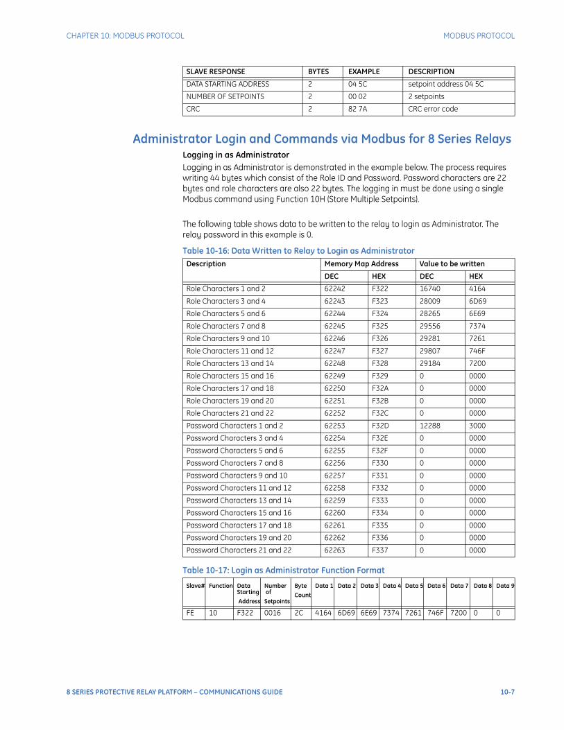
CHAPTER 10: MODBUS PROTOCOL MODBUS PROTOCOL
Administrator Login and Commands via Modbus for 8 Series RelaysLogging in as AdministratorLogging in as Administrator is demonstrated in the example below. The process requires writing 44 bytes which consist of the Role ID and Password. Password characters are 22 bytes and role characters are also 22 bytes. The logging in must be done using a single Modbus command using Function 10H (Store Multiple Setpoints).
The following table shows data to be written to the relay to login as Administrator. The relay password in this example is 0.
Table 10-16: Data Written to Relay to Login as Administrator
Table 10-17: Login as Administrator Function Format
DATA STARTING ADDRESS 2 04 5C setpoint address 04 5C
NUMBER OF SETPOINTS 2 00 02 2 setpoints
CRC 2 82 7A CRC error code
SLAVE RESPONSE BYTES EXAMPLE DESCRIPTION
Description Memory Map Address Value to be written
DEC HEX DEC HEX
Role Characters 1 and 2 62242 F322 16740 4164
Role Characters 3 and 4 62243 F323 28009 6D69
Role Characters 5 and 6 62244 F324 28265 6E69
Role Characters 7 and 8 62245 F325 29556 7374
Role Characters 9 and 10 62246 F326 29281 7261
Role Characters 11 and 12 62247 F327 29807 746F
Role Characters 13 and 14 62248 F328 29184 7200
Role Characters 15 and 16 62249 F329 0 0000
Role Characters 17 and 18 62250 F32A 0 0000
Role Characters 19 and 20 62251 F32B 0 0000
Role Characters 21 and 22 62252 F32C 0 0000
Password Characters 1 and 2 62253 F32D 12288 3000
Password Characters 3 and 4 62254 F32E 0 0000
Password Characters 5 and 6 62255 F32F 0 0000
Password Characters 7 and 8 62256 F330 0 0000
Password Characters 9 and 10 62257 F331 0 0000
Password Characters 11 and 12 62258 F332 0 0000
Password Characters 13 and 14 62259 F333 0 0000
Password Characters 15 and 16 62260 F334 0 0000
Password Characters 17 and 18 62261 F335 0 0000
Password Characters 19 and 20 62262 F336 0 0000
Password Characters 21 and 22 62263 F337 0 0000
Slave# Function Data Starting Address
Number of
Setpoints
Byte
Count
Data 1 Data 2 Data 3 Data 4 Data 5 Data 6 Data 7 Data 8 Data 9
FE 10 F322 0016 2C 4164 6D69 6E69 7374 7261 746F 7200 0 0
8 SERIES PROTECTIVE RELAY PLATFORM – COMMUNICATIONS GUIDE 10-7
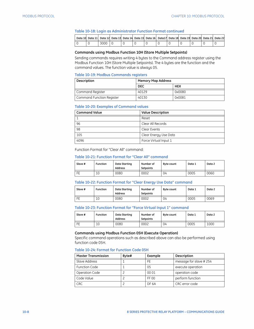
MODBUS PROTOCOL CHAPTER 10: MODBUS PROTOCOL
Table 10-18: Login as Administrator Function Format continued
Commands using Modbus Function 10H (Store Multiple Setpoints)Sending commands requires writing 4 bytes to the Command address register using the Modbus Function 10H (Store Multiple Setpoints). The 4 bytes are the function and the command values. The function value is always 05.
Table 10-19: Modbus Commands registers
Table 10-20: Examples of Command values
Function Format for “Clear All” command:
Table 10-21: Function Format for “Clear All” command
Table 10-22: Function Format for “Clear Energy Use Data” command
Table 10-23: Function Format for “Force Virtual Input 1” command
Commands using Modbus Function 05H (Execute Operation) Specific command operations such as described above can also be performed using function code 05H.
Table 10-24: Format for Function Code 05H
Data 10 Data 11 Data 12 Data 13 Data 14 Data 15 Data 16 Data17 Data 18 Data 19 Data 20 Data 21 Data 22
0 0 3000 0 0 0 0 0 0 0 0 0 0
Description Memory Map Address
DEC HEX
Command Register 40129 0x0080
Command Function Register 40130 0x0081
Command Value Value Description
1 Reset
96 Clear All Records
98 Clear Events
105 Clear Energy Use Data
4096 Force Virtual Input 1
Slave # Function Data Starting
Address
Number of
Setpoints
Byte count Data 1 Data 2
FE 10 0080 0002 04 0005 0060
Slave # Function Data Starting
Address
Number of
Setpoints
Byte count Data 1 Data 2
FE 10 0080 0002 04 0005 0069
Slave # Function Data Starting
Address
Number of
Setpoints
Byte count Data 1 Data 2
FE 10 0080 0002 04 0005 1000
Master Transmission Byte# Example Description
Slave Address 1 FE message for slave # 254
Function Code 1 05 execute operation
Operation Code 2 00 01 operation code
Code Value 2 FF 00 perform function
CRC 2 DF 6A CRC error code
10-8 8 SERIES PROTECTIVE RELAY PLATFORM – COMMUNICATIONS GUIDE
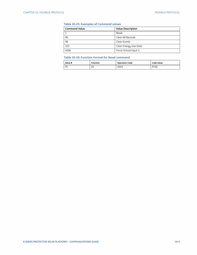
CHAPTER 10: MODBUS PROTOCOL MODBUS PROTOCOL
Table 10-25: Examples of Command values
Table 10-26: Function Format for Reset command
Command Value Value Description
1 Reset
96 Clear All Records
98 Clear Events
105 Clear Energy Use Data
4096 Force Virtual Input 1
Slave # Function Operation Code Code Value
FE 05 0001 FF00
8 SERIES PROTECTIVE RELAY PLATFORM – COMMUNICATIONS GUIDE 10-9

MODBUS PROTOCOL CHAPTER 10: MODBUS PROTOCOL
10-10 8 SERIES PROTECTIVE RELAY PLATFORM – COMMUNICATIONS GUIDE
8 Series Protective Relay Platform
Chapter 11: Modbus Memory Map
GEGrid Solutions
Modbus Memory Map
Reading the Event Recorder
To read the entire event recorder contents (the only available format), use the following filename:Evt.evt
Reading Transient Recorder
Familiarity with the Transient recorder feature is required to understand the following description. The Oscillography_ Number_of_Triggers register is incremented by one every time a new oscillography file is triggered (captured) and cleared to zero when oscillography data is cleared. When a new trigger occurs, the associated oscillography file is assigned a file identifier number equal to the incremented value of the register; the newest file number is equal to the Oscillography_Number_of_Triggers register. This register can be used to determine if any new data has been captured by periodically reading it to see if the value has changed; if the number has increased then new data is available.The Oscillography Number of Records register specifies the maximum number of files (and the number of cycles of data per file) that can be stored in the memory of the relay.The Oscillography Available Records register specifies the actual number of files that are stored and still available to be read out of the relay. Writing “Yes” (i.e. the value 1) to the Oscillography Clear Data register clears oscillography data files, clears both the Oscillography Number of Triggers and Oscillography Available Records registers to zero, and sets the Oscillography Last Cleared Date to the present date and time.To read binary COMTRADE oscillography files, read the following filenames:OSCnnnn.CFG and OSCnnn.DATReplace the “nnn” with the desired oscillography trigger number. For ASCII format, use the following filenames:OSCAnnnn.CFG and OSCAnnn.DAT
8 SERIES PROTECTIVE RELAY PLATFORM – COMMUNICATIONS GUIDE 11-1

READING FAULT REPORTS CHAPTER 11: MODBUS MEMORY MAP
Reading Fault Reports
Fault report data is available via the file retrieval mechanism in 8 Series relay. The filename is FaultReport1_#####.txt and the ##### refers to the fault report record number.The fault report number is a counter that indicates how many fault reports have ever occurred. Only the last fifteen fault reports are available for retrieval; a request for a non-existent fault report file yields a null file.The current value fault report counter is available in “Number of Fault Reports” Modbus register.
Accessing Data via the User Map
The 8 Series relay has a powerful feature, called the User Map, which allows a computer to read up to 125 non-consecutive data registers (setpoints or actual values) by using one Modbus packet. It is often necessary for a master computer to continuously poll various values in each of the connected slave relays. If these values are scattered throughout the memory map, reading them would require numerous transmissions and would burden the communication link. The User Map can be programmed to join any memory map address to one in the block of consecutive User Map locations, so that they can be accessed by reading these consecutive locations.The 8 Series relay contains a user-definable area in the Modbus memory map. This area allows re-mapping of the addresses of any Actual Values registers. The User Definable area has two sections.
1. A Register Index area (40524 to 40648) that contains 125 Actual Values register addresses
2. A Register area (30524 to 30648) that contains the data at the addresses in the Register Index
Register data that is separated in the rest of the memory map may be re-mapped to adjacent register addresses in the user-definable registers area. This is accomplished by writing to register addresses in the user-definable register index area. This allows for improved throughput of data and can eliminate the need for multiple read command sequences. The user-definable register index is stored as a setpoint and therefore it is “remembered” even when the power is removed.Default User MapCommon actual values have been defaulted for the user. Below are the default registers.
Table 11-1: Default User Map
User Map Address Description Modbus Address
User Map Address 1,2 Device Status 30712 30713
User Map Address 3,4 LED Status 30708 30709
User Map Address 5,6 Contact Input 1-32 30700 30701
User Map Address 7,8 Contact Output 1-32 30706 30707
User Map Address 9,10 Virtual Input Status 1-32 30714 30715
User Map Address 11, 12 Virtual Output Status 1-32 30718 30719
User Map Address 13,14 Remote Input 1-32 30728 30729
User Map Address 15,16 Remote Output 1-32 30736 30737
User Map Address 17,18 Ia 31270 31271
User Map Address 19,20 Ib 31272 31273
11-2 8 SERIES PROTECTIVE RELAY PLATFORM – COMMUNICATIONS GUIDE

CHAPTER 11: MODBUS MEMORY MAP MEMORY MAP ORGANIZATION
The 8 Series relay supports 32-bit Modbus items to be configured in the user map. When such an address is configured in the user map for example at user map address 1, user map address 2 is also consumed by the same item irrespective of the address assigned in address 2.
Memory Map Organization
The 8 Series relay Memory Map describes all the data registers that can be accessed via serial communications. The Memory Map address range is grouped into several categories as outlined in the following table. All memory map locations are two byte (16 bit) values. The remaining pages of this chapter list all locations of the Memory Map. Addresses for all locations are shown in hexadecimal. Consult the range, step, units, and the data format (listed after the memory map) to interpret register values.Many Modbus communications drivers add 40001d to the actual address of the register addresses. For example, if address 0h was to be read, then 40001d would be the address required by the Modbus communications driver; similarly, if address 320h (800d) was to be read, then 40801d would be the address required by the Modbus communications driver.
Table 11-2: Memory Map Organization
Using the Memory Map
Reading CO OutputsCO Outputs are used to show the state of the output relays in the 8-Series device (internal to the device). For example, on the 869 relay the Trip and Close contacts have voltage monitoring inputs. The Trip and Close Circuit Monitoring feature uses the voltage input to monitor the trip and to close coil circuit integrity.
User Map Address 21,22 Ic 31274 31275
User Map Address 23,24 In 31278 31279
User Map Address 25,26 Iavg 31295 31296
User Map Address 27,28 Ig 31276 31277
User Map Address Description Modbus Address
Memory Map Section Address Range Description
Product ID 0000h to 007Fh Identification and revision information.
Commands 0080h to 00FFh Substitute command locations. Read and write access.
User Map 0100h to 01FFh User Map Values and Addresses. See the previous section for details.
Actual Values 0200h to 0FFFh Actual values data. Read Only.
Setpoints 1000h to 1FFFh Setpoints data. Read and Write.
Event Recorder, Trace Memory, and Data Logger
2000h to 2FFFh See relevant sections in this chapter for details.
Reserved 3000h to 3FFFh Reserved for future use.
Factory Service Data 4000h to FFFFh Reserved.
8 SERIES PROTECTIVE RELAY PLATFORM – COMMUNICATIONS GUIDE 11-3
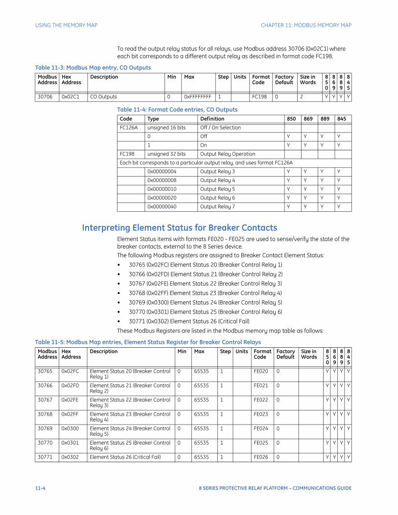
USING THE MEMORY MAP CHAPTER 11: MODBUS MEMORY MAP
To read the output relay status for all relays, use Modbus address 30706 (0x02C1) where each bit corresponds to a different output relay as described in format code FC198.
Table 11-3: Modbus Map entry, CO Outputs
Table 11-4: Format Code entries, CO Outputs
Interpreting Element Status for Breaker ContactsElement Status items with formats FE020 - FE025 are used to sense/verify the state of the breaker contacts, external to the 8 Series device. The following Modbus registers are assigned to Breaker Contact Element Status:
• 30765 (0x02FC) Element Status 20 (Breaker Control Relay 1)
• 30766 (0x02FD) Element Status 21 (Breaker Control Relay 2)
• 30767 (0x02FE) Element Status 22 (Breaker Control Relay 3)
• 30768 (0x02FF) Element Status 23 (Breaker Control Relay 4)
• 30769 (0x0300) Element Status 24 (Breaker Control Relay 5)
• 30770 (0x0301) Element Status 25 (Breaker Control Relay 6)
• 30771 (0x0302) Element Status 26 (Critical Fail)
These Modbus Registers are listed in the Modbus memory map table as follows:
Table 11-5: Modbus Map entries, Element Status Register for Breaker Control Relays
Modbus Address
Hex Address
Description Min Max Step Units Format Code
Factory Default
Size in Words
850
869
889
845
30706 0x02C1 CO Outputs 0 0xFFFFFFFF 1 FC198 0 2 Y Y Y Y
Code Type Definition 850 869 889 845
FC126A unsigned 16 bits Off / On Selection
0 Off Y Y Y Y
1 On Y Y Y Y
FC198 unsigned 32 bits Output Relay Operation
Each bit corresponds to a particular output relay, and uses format FC126A
0x00000004 Output Relay 3 Y Y Y Y
0x00000008 Output Relay 4 Y Y Y Y
0x00000010 Output Relay 5 Y Y Y Y
0x00000020 Output Relay 6 Y Y Y Y
0x00000040 Output Relay 7 Y Y Y Y
Modbus Address
Hex Address
Description Min Max Step Units Format Code
Factory Default
Size in Words
850
869
889
845
30765 0x02FC Element Status 20 (Breaker Control Relay 1)
0 65535 1 FE020 0 Y Y Y Y
30766 0x02FD Element Status 21 (Breaker Control Relay 2)
0 65535 1 FE021 0 Y Y Y Y
30767 0x02FE Element Status 22 (Breaker Control Relay 3)
0 65535 1 FE022 0 Y Y Y Y
30768 0x02FF Element Status 23 (Breaker Control Relay 4)
0 65535 1 FE023 0 Y Y Y Y
30769 0x0300 Element Status 24 (Breaker Control Relay 5)
0 65535 1 FE024 0 Y Y Y Y
30770 0x0301 Element Status 25 (Breaker Control Relay 6)
0 65535 1 FE025 0 Y Y Y Y
30771 0x0302 Element Status 26 (Critical Fail) 0 65535 1 FE026 0 Y Y Y Y
11-4 8 SERIES PROTECTIVE RELAY PLATFORM – COMMUNICATIONS GUIDE
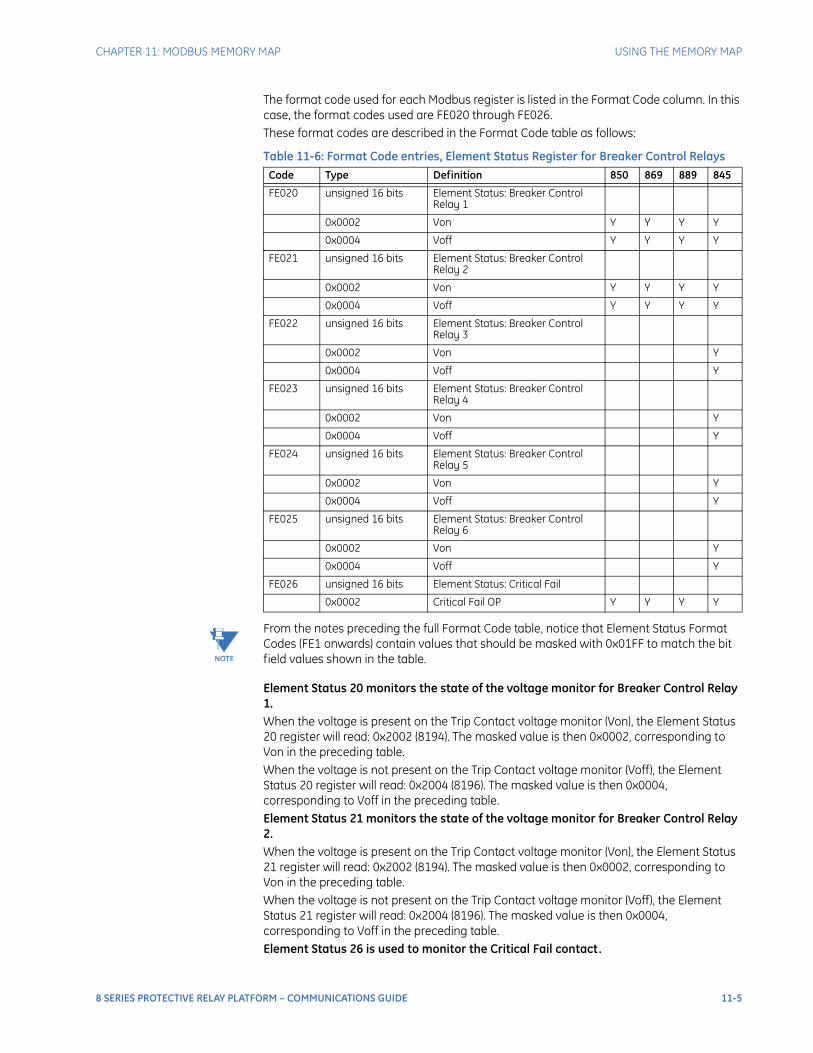
CHAPTER 11: MODBUS MEMORY MAP USING THE MEMORY MAP
The format code used for each Modbus register is listed in the Format Code column. In this case, the format codes used are FE020 through FE026.These format codes are described in the Format Code table as follows:
Table 11-6: Format Code entries, Element Status Register for Breaker Control Relays
NOTE
NOTE: From the notes preceding the full Format Code table, notice that Element Status Format Codes (FE1 onwards) contain values that should be masked with 0x01FF to match the bit field values shown in the table.
Element Status 20 monitors the state of the voltage monitor for Breaker Control Relay 1.When the voltage is present on the Trip Contact voltage monitor (Von), the Element Status 20 register will read: 0x2002 (8194). The masked value is then 0x0002, corresponding to Von in the preceding table.When the voltage is not present on the Trip Contact voltage monitor (Voff), the Element Status 20 register will read: 0x2004 (8196). The masked value is then 0x0004, corresponding to Voff in the preceding table.Element Status 21 monitors the state of the voltage monitor for Breaker Control Relay 2.When the voltage is present on the Trip Contact voltage monitor (Von), the Element Status 21 register will read: 0x2002 (8194). The masked value is then 0x0002, corresponding to Von in the preceding table.When the voltage is not present on the Trip Contact voltage monitor (Voff), the Element Status 21 register will read: 0x2004 (8196). The masked value is then 0x0004, corresponding to Voff in the preceding table.Element Status 26 is used to monitor the Critical Fail contact.
Code Type Definition 850 869 889 845
FE020 unsigned 16 bits Element Status: Breaker Control Relay 1
0x0002 Von Y Y Y Y
0x0004 Voff Y Y Y Y
FE021 unsigned 16 bits Element Status: Breaker Control Relay 2
0x0002 Von Y Y Y Y
0x0004 Voff Y Y Y Y
FE022 unsigned 16 bits Element Status: Breaker Control Relay 3
0x0002 Von Y
0x0004 Voff Y
FE023 unsigned 16 bits Element Status: Breaker Control Relay 4
0x0002 Von Y
0x0004 Voff Y
FE024 unsigned 16 bits Element Status: Breaker Control Relay 5
0x0002 Von Y
0x0004 Voff Y
FE025 unsigned 16 bits Element Status: Breaker Control Relay 6
0x0002 Von Y
0x0004 Voff Y
FE026 unsigned 16 bits Element Status: Critical Fail
0x0002 Critical Fail OP Y Y Y Y
8 SERIES PROTECTIVE RELAY PLATFORM – COMMUNICATIONS GUIDE 11-5
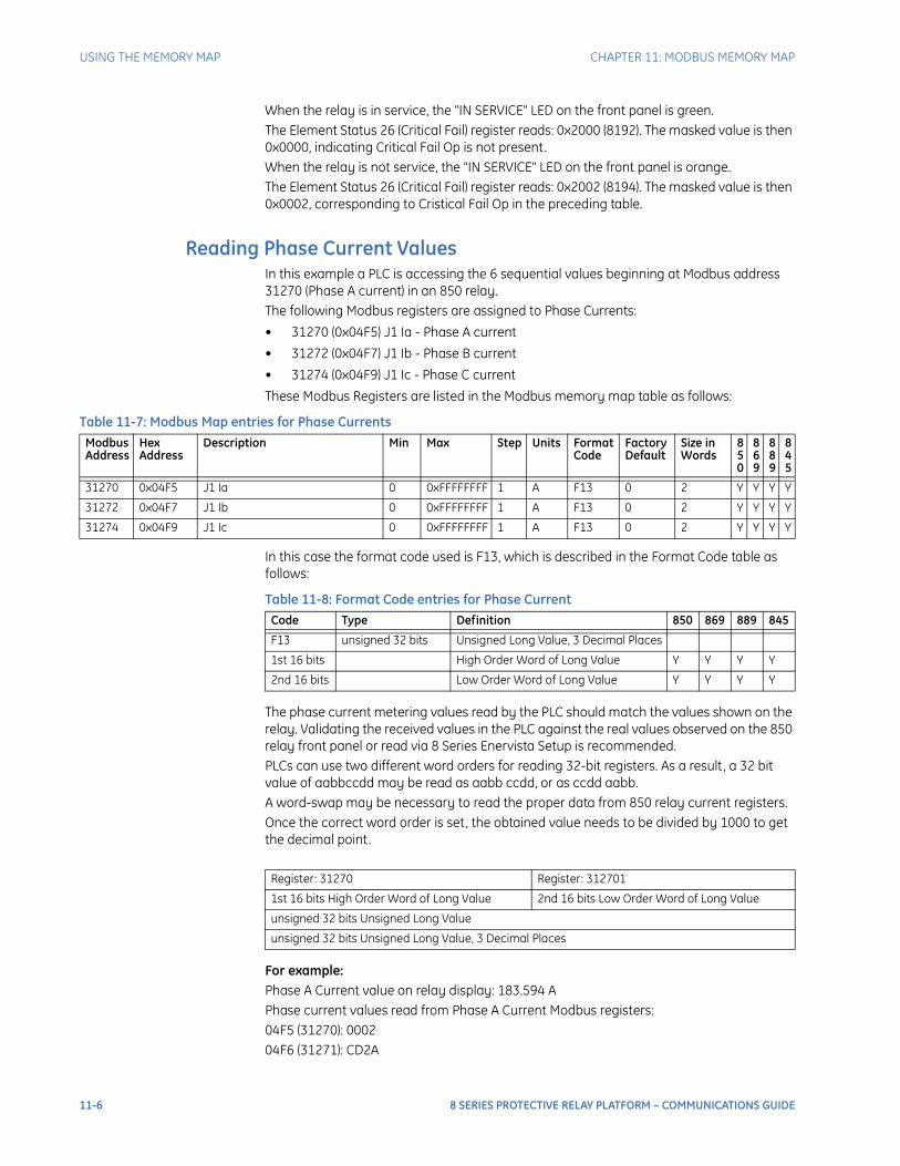
USING THE MEMORY MAP CHAPTER 11: MODBUS MEMORY MAP
When the relay is in service, the "IN SERVICE" LED on the front panel is green.The Element Status 26 (Critical Fail) register reads: 0x2000 (8192). The masked value is then 0x0000, indicating Critical Fail Op is not present.When the relay is not service, the "IN SERVICE" LED on the front panel is orange.The Element Status 26 (Critical Fail) register reads: 0x2002 (8194). The masked value is then 0x0002, corresponding to Cristical Fail Op in the preceding table.
Reading Phase Current ValuesIn this example a PLC is accessing the 6 sequential values beginning at Modbus address 31270 (Phase A current) in an 850 relay.The following Modbus registers are assigned to Phase Currents:
• 31270 (0x04F5) J1 Ia - Phase A current
• 31272 (0x04F7) J1 Ib - Phase B current
• 31274 (0x04F9) J1 Ic - Phase C current
These Modbus Registers are listed in the Modbus memory map table as follows:
Table 11-7: Modbus Map entries for Phase Currents
In this case the format code used is F13, which is described in the Format Code table as follows:
Table 11-8: Format Code entries for Phase Current
The phase current metering values read by the PLC should match the values shown on the relay. Validating the received values in the PLC against the real values observed on the 850 relay front panel or read via 8 Series Enervista Setup is recommended.PLCs can use two different word orders for reading 32-bit registers. As a result, a 32 bit value of aabbccdd may be read as aabb ccdd, or as ccdd aabb.A word-swap may be necessary to read the proper data from 850 relay current registers.Once the correct word order is set, the obtained value needs to be divided by 1000 to get the decimal point.
For example:Phase A Current value on relay display: 183.594 APhase current values read from Phase A Current Modbus registers:04F5 (31270): 000204F6 (31271): CD2A
Modbus Address
Hex Address
Description Min Max Step Units Format Code
Factory Default
Size in Words
850
869
889
845
31270 0x04F5 J1 Ia 0 0xFFFFFFFF 1 A F13 0 2 Y Y Y Y
31272 0x04F7 J1 Ib 0 0xFFFFFFFF 1 A F13 0 2 Y Y Y Y
31274 0x04F9 J1 Ic 0 0xFFFFFFFF 1 A F13 0 2 Y Y Y Y
Code Type Definition 850 869 889 845
F13 unsigned 32 bits Unsigned Long Value, 3 Decimal Places
1st 16 bits High Order Word of Long Value Y Y Y Y
2nd 16 bits Low Order Word of Long Value Y Y Y Y
Register: 31270 Register: 312701
1st 16 bits High Order Word of Long Value 2nd 16 bits Low Order Word of Long Value
unsigned 32 bits Unsigned Long Value
unsigned 32 bits Unsigned Long Value, 3 Decimal Places
11-6 8 SERIES PROTECTIVE RELAY PLATFORM – COMMUNICATIONS GUIDE

CHAPTER 11: MODBUS MEMORY MAP MODBUS MEMORY MAP
Combine the two 16 bit values into a 32 bit unsigned value: 183594Apply the decimal point rule (divide by 1000): 183.594 A
MODBUS memory map
Register: 31270 Register: 312701
0002 CD2A
183594
183.594
Modbus Address
Hex Address
Description Min Max Step Units Format Code
Factory Default
Size in Words
850
869
889
845
Actual Values
Product Information
30001 0x0000 Product Code 0 65535 1 F0 0 1 Y Y Y Y
30002 0x0001 Hardware Revision 0 26 1 FC110 1 1 Y Y Y Y
30003 0x0002 Firmware Version 0 65535 1 F2 160 1 Y Y Y Y
30005 0x0004 Boot 0 65535 1 F2 0 1 Y Y Y Y
30006 0x0005 Firmware Date 0x010107D8 0x0C1F082E 1 F53 16844760 2 Y Y Y Y
30008 0x0007 Firmware Time 0 0x173B3B63 1 F54 0 2 Y Y Y Y
30010 0x0009 Boot Date 0x010107D8 0x0C1F082E 1 F53 16844760 2 Y Y Y Y
30012 0x000B Boot Time 0 0x173B3B63 1 F54 0 2 Y Y Y Y
30014 0x000D Product Serial # 0 65535 1 F60_12 Serial 6 Y Y Y Y
30021 0x0014 Order Code 0 65535 1 F60_34 OrderCode 17 Y Y Y Y
30038 0x0025 MAC Address 1 0 65535 1 F60_6A 0 3 Y Y Y Y
30047 0x002E Comms CPU fw Version 0 65535 1 F2 0 1 Y Y Y Y
30049 0x0030 Boot 0 65535 1 F2 0 1 Y Y Y Y
30050 0x0031 Comms CPU Firmware Date
0x010107D8 0x0C1F082E 1 F53 16844760 2 Y Y Y Y
30052 0x0033 Comms CPU Firmware Time
0 0x173B3B63 1 F54 0 2 Y Y Y Y
30054 0x0035 Boot Date 0x010107D8 0x0C1F082E 1 F53 16844760 2 Y Y Y Y
30056 0x0037 Boot Time 0 0x173B3B63 1 F54 0 2 Y Y Y Y
30058 0x0039 MAC Address 1 0 65535 1 F60_6A 0 3 Y Y Y Y
30061 0x003C MAC Address 2 0 65535 1 F60_6A 0 3 Y Y Y Y
30067 0x0042 FPGA Firmware Version 0 0xFFFFFFFF 1 F71 0 2 Y Y Y Y
30069 0x0044 IO F CPLD 0 0xFFFFFFFF 1 F71 0 2 Y Y Y Y
30071 0x0046 IO G CPLD 0 0xFFFFFFFF 1 F71 0 2 Y Y Y Y
30075 0x004A AN J CPLD 0 0xFFFFFFFF 1 F71 0 2 Y Y Y Y
30077 0x004C AN K CPLD 0 0xFFFFFFFF 1 F71 0 2 Y Y Y Y
30079 0x004E Display CPLD 0 0xFFFFFFFF 1 F71 0 2 Y Y Y Y
Time
30241 0x00F0 Time 0 0x173B3B63 1 F54 0 2 Y Y Y Y
30243 0x00F2 Date 0x010107D8 0x0C1F082E 1 F53 16844760 2 Y Y Y Y
30245 0x00F4 RTC Time 0 0xFFFFFFFF 1 s F52 0 2 Y Y Y Y
30247 0x00F6 System Clock 0 0xFFFFFFFF 1 s F52 0 2 Y Y Y Y
8 SERIES PROTECTIVE RELAY PLATFORM – COMMUNICATIONS GUIDE 11-7
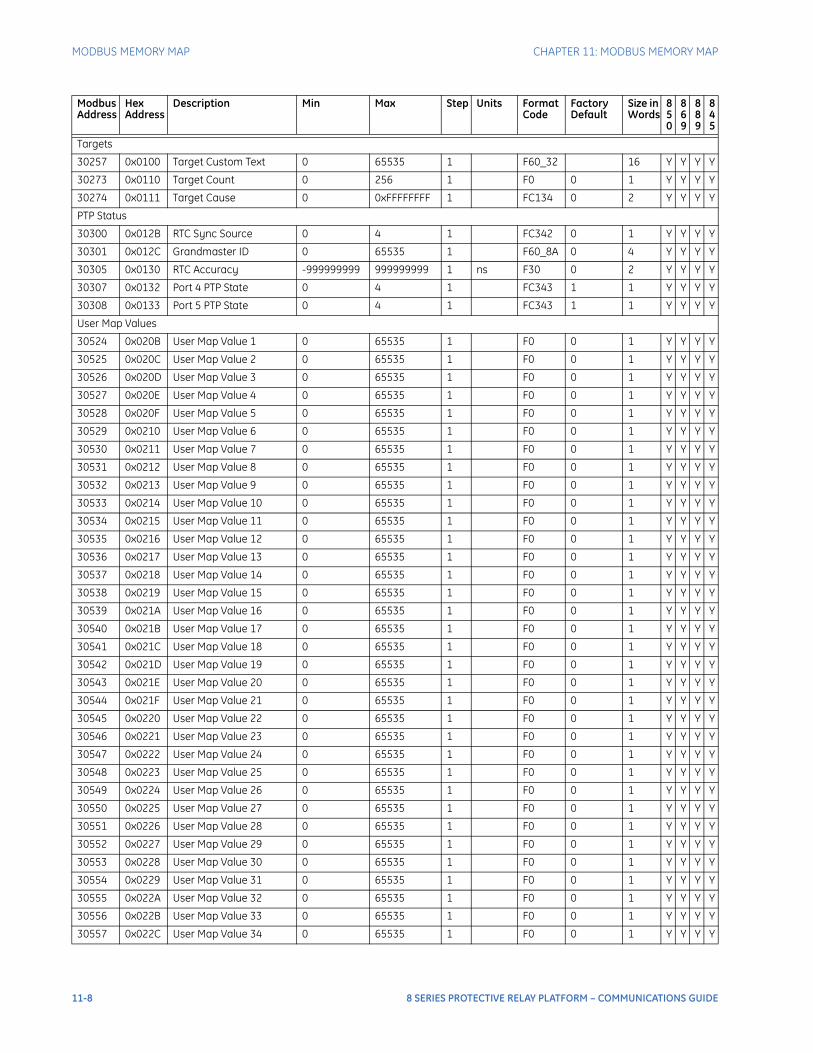
MODBUS MEMORY MAP CHAPTER 11: MODBUS MEMORY MAP
Targets
30257 0x0100 Target Custom Text 0 65535 1 F60_32 16 Y Y Y Y
30273 0x0110 Target Count 0 256 1 F0 0 1 Y Y Y Y
30274 0x0111 Target Cause 0 0xFFFFFFFF 1 FC134 0 2 Y Y Y Y
PTP Status
30300 0x012B RTC Sync Source 0 4 1 FC342 0 1 Y Y Y Y
30301 0x012C Grandmaster ID 0 65535 1 F60_8A 0 4 Y Y Y Y
30305 0x0130 RTC Accuracy -999999999 999999999 1 ns F30 0 2 Y Y Y Y
30307 0x0132 Port 4 PTP State 0 4 1 FC343 1 1 Y Y Y Y
30308 0x0133 Port 5 PTP State 0 4 1 FC343 1 1 Y Y Y Y
User Map Values
30524 0x020B User Map Value 1 0 65535 1 F0 0 1 Y Y Y Y
30525 0x020C User Map Value 2 0 65535 1 F0 0 1 Y Y Y Y
30526 0x020D User Map Value 3 0 65535 1 F0 0 1 Y Y Y Y
30527 0x020E User Map Value 4 0 65535 1 F0 0 1 Y Y Y Y
30528 0x020F User Map Value 5 0 65535 1 F0 0 1 Y Y Y Y
30529 0x0210 User Map Value 6 0 65535 1 F0 0 1 Y Y Y Y
30530 0x0211 User Map Value 7 0 65535 1 F0 0 1 Y Y Y Y
30531 0x0212 User Map Value 8 0 65535 1 F0 0 1 Y Y Y Y
30532 0x0213 User Map Value 9 0 65535 1 F0 0 1 Y Y Y Y
30533 0x0214 User Map Value 10 0 65535 1 F0 0 1 Y Y Y Y
30534 0x0215 User Map Value 11 0 65535 1 F0 0 1 Y Y Y Y
30535 0x0216 User Map Value 12 0 65535 1 F0 0 1 Y Y Y Y
30536 0x0217 User Map Value 13 0 65535 1 F0 0 1 Y Y Y Y
30537 0x0218 User Map Value 14 0 65535 1 F0 0 1 Y Y Y Y
30538 0x0219 User Map Value 15 0 65535 1 F0 0 1 Y Y Y Y
30539 0x021A User Map Value 16 0 65535 1 F0 0 1 Y Y Y Y
30540 0x021B User Map Value 17 0 65535 1 F0 0 1 Y Y Y Y
30541 0x021C User Map Value 18 0 65535 1 F0 0 1 Y Y Y Y
30542 0x021D User Map Value 19 0 65535 1 F0 0 1 Y Y Y Y
30543 0x021E User Map Value 20 0 65535 1 F0 0 1 Y Y Y Y
30544 0x021F User Map Value 21 0 65535 1 F0 0 1 Y Y Y Y
30545 0x0220 User Map Value 22 0 65535 1 F0 0 1 Y Y Y Y
30546 0x0221 User Map Value 23 0 65535 1 F0 0 1 Y Y Y Y
30547 0x0222 User Map Value 24 0 65535 1 F0 0 1 Y Y Y Y
30548 0x0223 User Map Value 25 0 65535 1 F0 0 1 Y Y Y Y
30549 0x0224 User Map Value 26 0 65535 1 F0 0 1 Y Y Y Y
30550 0x0225 User Map Value 27 0 65535 1 F0 0 1 Y Y Y Y
30551 0x0226 User Map Value 28 0 65535 1 F0 0 1 Y Y Y Y
30552 0x0227 User Map Value 29 0 65535 1 F0 0 1 Y Y Y Y
30553 0x0228 User Map Value 30 0 65535 1 F0 0 1 Y Y Y Y
30554 0x0229 User Map Value 31 0 65535 1 F0 0 1 Y Y Y Y
30555 0x022A User Map Value 32 0 65535 1 F0 0 1 Y Y Y Y
30556 0x022B User Map Value 33 0 65535 1 F0 0 1 Y Y Y Y
30557 0x022C User Map Value 34 0 65535 1 F0 0 1 Y Y Y Y
Modbus Address
Hex Address
Description Min Max Step Units Format Code
Factory Default
Size in Words
850
869
889
845
11-8 8 SERIES PROTECTIVE RELAY PLATFORM – COMMUNICATIONS GUIDE

CHAPTER 11: MODBUS MEMORY MAP MODBUS MEMORY MAP
30558 0x022D User Map Value 35 0 65535 1 F0 0 1 Y Y Y Y
30559 0x022E User Map Value 36 0 65535 1 F0 0 1 Y Y Y Y
30560 0x022F User Map Value 37 0 65535 1 F0 0 1 Y Y Y Y
30561 0x0230 User Map Value 38 0 65535 1 F0 0 1 Y Y Y Y
30562 0x0231 User Map Value 39 0 65535 1 F0 0 1 Y Y Y Y
30563 0x0232 User Map Value 40 0 65535 1 F0 0 1 Y Y Y Y
30564 0x0233 User Map Value 41 0 65535 1 F0 0 1 Y Y Y Y
30565 0x0234 User Map Value 42 0 65535 1 F0 0 1 Y Y Y Y
30566 0x0235 User Map Value 43 0 65535 1 F0 0 1 Y Y Y Y
30567 0x0236 User Map Value 44 0 65535 1 F0 0 1 Y Y Y Y
30568 0x0237 User Map Value 45 0 65535 1 F0 0 1 Y Y Y Y
30569 0x0238 User Map Value 46 0 65535 1 F0 0 1 Y Y Y Y
30570 0x0239 User Map Value 47 0 65535 1 F0 0 1 Y Y Y Y
30571 0x023A User Map Value 48 0 65535 1 F0 0 1 Y Y Y Y
30572 0x023B User Map Value 49 0 65535 1 F0 0 1 Y Y Y Y
30573 0x023C User Map Value 50 0 65535 1 F0 0 1 Y Y Y Y
30574 0x023D User Map Value 51 0 65535 1 F0 0 1 Y Y Y Y
30575 0x023E User Map Value 52 0 65535 1 F0 0 1 Y Y Y Y
30576 0x023F User Map Value 53 0 65535 1 F0 0 1 Y Y Y Y
30577 0x0240 User Map Value 54 0 65535 1 F0 0 1 Y Y Y Y
30578 0x0241 User Map Value 55 0 65535 1 F0 0 1 Y Y Y Y
30579 0x0242 User Map Value 56 0 65535 1 F0 0 1 Y Y Y Y
30580 0x0243 User Map Value 57 0 65535 1 F0 0 1 Y Y Y Y
30581 0x0244 User Map Value 58 0 65535 1 F0 0 1 Y Y Y Y
30582 0x0245 User Map Value 59 0 65535 1 F0 0 1 Y Y Y Y
30583 0x0246 User Map Value 60 0 65535 1 F0 0 1 Y Y Y Y
30584 0x0247 User Map Value 61 0 65535 1 F0 0 1 Y Y Y Y
30585 0x0248 User Map Value 62 0 65535 1 F0 0 1 Y Y Y Y
30586 0x0249 User Map Value 63 0 65535 1 F0 0 1 Y Y Y Y
30587 0x024A User Map Value 64 0 65535 1 F0 0 1 Y Y Y Y
30588 0x024B User Map Value 65 0 65535 1 F0 0 1 Y Y Y Y
30589 0x024C User Map Value 66 0 65535 1 F0 0 1 Y Y Y Y
30590 0x024D User Map Value 67 0 65535 1 F0 0 1 Y Y Y Y
30591 0x024E User Map Value 68 0 65535 1 F0 0 1 Y Y Y Y
30592 0x024F User Map Value 69 0 65535 1 F0 0 1 Y Y Y Y
30593 0x0250 User Map Value 70 0 65535 1 F0 0 1 Y Y Y Y
30594 0x0251 User Map Value 71 0 65535 1 F0 0 1 Y Y Y Y
30595 0x0252 User Map Value 72 0 65535 1 F0 0 1 Y Y Y Y
30596 0x0253 User Map Value 73 0 65535 1 F0 0 1 Y Y Y Y
30597 0x0254 User Map Value 74 0 65535 1 F0 0 1 Y Y Y Y
30598 0x0255 User Map Value 75 0 65535 1 F0 0 1 Y Y Y Y
30599 0x0256 User Map Value 76 0 65535 1 F0 0 1 Y Y Y Y
30600 0x0257 User Map Value 77 0 65535 1 F0 0 1 Y Y Y Y
30601 0x0258 User Map Value 78 0 65535 1 F0 0 1 Y Y Y Y
30602 0x0259 User Map Value 79 0 65535 1 F0 0 1 Y Y Y Y
Modbus Address
Hex Address
Description Min Max Step Units Format Code
Factory Default
Size in Words
850
869
889
845
8 SERIES PROTECTIVE RELAY PLATFORM – COMMUNICATIONS GUIDE 11-9
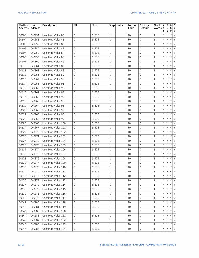
MODBUS MEMORY MAP CHAPTER 11: MODBUS MEMORY MAP
30603 0x025A User Map Value 80 0 65535 1 F0 0 1 Y Y Y Y
30604 0x025B User Map Value 81 0 65535 1 F0 0 1 Y Y Y Y
30605 0x025C User Map Value 82 0 65535 1 F0 0 1 Y Y Y Y
30606 0x025D User Map Value 83 0 65535 1 F0 0 1 Y Y Y Y
30607 0x025E User Map Value 84 0 65535 1 F0 0 1 Y Y Y Y
30608 0x025F User Map Value 85 0 65535 1 F0 0 1 Y Y Y Y
30609 0x0260 User Map Value 86 0 65535 1 F0 0 1 Y Y Y Y
30610 0x0261 User Map Value 87 0 65535 1 F0 0 1 Y Y Y Y
30611 0x0262 User Map Value 88 0 65535 1 F0 0 1 Y Y Y Y
30612 0x0263 User Map Value 89 0 65535 1 F0 0 1 Y Y Y Y
30613 0x0264 User Map Value 90 0 65535 1 F0 0 1 Y Y Y Y
30614 0x0265 User Map Value 91 0 65535 1 F0 0 1 Y Y Y Y
30615 0x0266 User Map Value 92 0 65535 1 F0 0 1 Y Y Y Y
30616 0x0267 User Map Value 93 0 65535 1 F0 0 1 Y Y Y Y
30617 0x0268 User Map Value 94 0 65535 1 F0 0 1 Y Y Y Y
30618 0x0269 User Map Value 95 0 65535 1 F0 0 1 Y Y Y Y
30619 0x026A User Map Value 96 0 65535 1 F0 0 1 Y Y Y Y
30620 0x026B User Map Value 97 0 65535 1 F0 0 1 Y Y Y Y
30621 0x026C User Map Value 98 0 65535 1 F0 0 1 Y Y Y Y
30622 0x026D User Map Value 99 0 65535 1 F0 0 1 Y Y Y Y
30623 0x026E User Map Value 100 0 65535 1 F0 0 1 Y Y Y Y
30624 0x026F User Map Value 101 0 65535 1 F0 0 1 Y Y Y Y
30625 0x0270 User Map Value 102 0 65535 1 F0 0 1 Y Y Y Y
30626 0x0271 User Map Value 103 0 65535 1 F0 0 1 Y Y Y Y
30627 0x0272 User Map Value 104 0 65535 1 F0 0 1 Y Y Y Y
30628 0x0273 User Map Value 105 0 65535 1 F0 0 1 Y Y Y Y
30629 0x0274 User Map Value 106 0 65535 1 F0 0 1 Y Y Y Y
30630 0x0275 User Map Value 107 0 65535 1 F0 0 1 Y Y Y Y
30631 0x0276 User Map Value 108 0 65535 1 F0 0 1 Y Y Y Y
30632 0x0277 User Map Value 109 0 65535 1 F0 0 1 Y Y Y Y
30633 0x0278 User Map Value 110 0 65535 1 F0 0 1 Y Y Y Y
30634 0x0279 User Map Value 111 0 65535 1 F0 0 1 Y Y Y Y
30635 0x027A User Map Value 112 0 65535 1 F0 0 1 Y Y Y Y
30636 0x027B User Map Value 113 0 65535 1 F0 0 1 Y Y Y Y
30637 0x027C User Map Value 114 0 65535 1 F0 0 1 Y Y Y Y
30638 0x027D User Map Value 115 0 65535 1 F0 0 1 Y Y Y Y
30639 0x027E User Map Value 116 0 65535 1 F0 0 1 Y Y Y Y
30640 0x027F User Map Value 117 0 65535 1 F0 0 1 Y Y Y Y
30641 0x0280 User Map Value 118 0 65535 1 F0 0 1 Y Y Y Y
30642 0x0281 User Map Value 119 0 65535 1 F0 0 1 Y Y Y Y
30643 0x0282 User Map Value 120 0 65535 1 F0 0 1 Y Y Y Y
30644 0x0283 User Map Value 121 0 65535 1 F0 0 1 Y Y Y Y
30645 0x0284 User Map Value 122 0 65535 1 F0 0 1 Y Y Y Y
30646 0x0285 User Map Value 123 0 65535 1 F0 0 1 Y Y Y Y
30647 0x0286 User Map Value 124 0 65535 1 F0 0 1 Y Y Y Y
Modbus Address
Hex Address
Description Min Max Step Units Format Code
Factory Default
Size in Words
850
869
889
845
11-10 8 SERIES PROTECTIVE RELAY PLATFORM – COMMUNICATIONS GUIDE
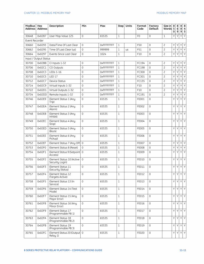
CHAPTER 11: MODBUS MEMORY MAP MODBUS MEMORY MAP
30648 0x0287 User Map Value 125 0 65535 1 F0 0 1 Y Y Y Y
Event Recorder
30660 0x0293 Date/Time Of Last Clear 0 0xFFFFFFFF 1 F50 0 2 Y Y Y Y
30662 0x0295 Time Of Last Clear (us) 0 999999 1 us F51 0 2 Y Y Y Y
30664 0x0297 Events Since Last Clear 0 1024 1 F10 0 2 Y Y Y Y
Input / Output Status
30700 0x02BB CI Inputs 1-32 0 0xFFFFFFFF 1 FC194 0 2 Y Y Y Y
30706 0x02C1 CO Outputs 0 0xFFFFFFFF 1 FC198 0 2 Y Y Y Y
30708 0x02C3 LEDs 1-16 0 0xFFFFFFFF 1 FC300 0 2 Y Y Y Y
30710 0x02C5 LED 17 0 0xFFFFFFFF 1 FC301 0 2 Y Y Y Y
30712 0x02C7 Device Status 0 0xFFFFFFFF 1 FC135 0 2 Y Y Y Y
30714 0x02C9 Virtual Inputs 1-32 0 0xFFFFFFFF 1 F10 0 2 Y Y Y Y
30722 0x02D1 Virtual Outputs 1-32 0 0xFFFFFFFF 1 F10 0 2 Y Y Y Y
30734 0x02DD Remote Inputs 1-32 0 0xFFFFFFFF 1 FC191 0 2 Y Y Y Y
30746 0x02E9 Element Status 1 (Any Trip)
0 65535 1 FE001 0 Y Y Y Y
30747 0x02EA Element Status 2 (Any Alarm)
0 65535 1 FE002 0 Y Y Y Y
30748 0x02EB Element Status 3 (Any Inhibit)
0 65535 1 FE003 0 Y Y Y Y
30749 0x02EC Element Status 4 (Any Stop)
0 65535 1 FE004 0 Y Y Y Y
30750 0x02ED Element Status 5 (Any Block)
0 65535 1 FE005 0 Y Y Y Y
30751 0x02EE Element Status 6 (Any Pickup)
0 65535 1 FE006 0 Y Y Y Y
30752 0x02EF Element Status 7 (Any OP) 0 65535 1 FE007 0 Y Y Y Y
30753 0x02F0 Element Status 8 (Reset) 0 65535 1 FE008 0 Y Y Y Y
30754 0x02F1 Element Status 9 (Setpoint Access)
0 65535 1 FE009 0 Y Y Y Y
30755 0x02F2 Element Status 10 (Active Security Login)
0 65535 1 FE010 0 Y Y Y Y
30756 0x02F3 Element Status 11 (Security Status)
0 65535 1 FE011 0 Y Y Y Y
30757 0x02F4 Element Status 12 (Targets Active)
0 65535 1 FE012 0 Y Y Y Y
30758 0x02F5 Element Status 13 (In Service)
0 65535 1 FE013 0 Y Y Y Y
30759 0x02F6 Element Status 14 (Test Mode)
0 65535 1 FE014 0 Y Y Y Y
30760 0x02F7 Element Status 15 (Any Major Error)
0 65535 1 FE015 0 Y Y Y Y
30761 0x02F8 Element Status 16 (Any Minor Error)
0 65535 1 FE016 0 Y Y Y Y
30762 0x02F9 Element Status 17 (Programmable PB 1)
0 65535 1 FE017 0 Y Y Y Y
30763 0x02FA Element Status 18 (Programmable PB 2)
0 65535 1 FE018 0 Y Y Y Y
30764 0x02FB Element Status 19 (Programmable PB 3)
0 65535 1 FE019 0 Y Y Y Y
30765 0x02FC Element Status 20 (Output Relay 1)
0 65535 1 FE020 0 Y Y Y Y
Modbus Address
Hex Address
Description Min Max Step Units Format Code
Factory Default
Size in Words
850
869
889
845
8 SERIES PROTECTIVE RELAY PLATFORM – COMMUNICATIONS GUIDE 11-11
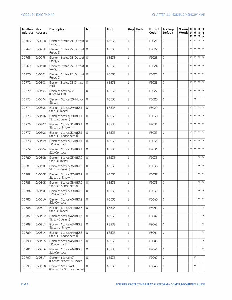
MODBUS MEMORY MAP CHAPTER 11: MODBUS MEMORY MAP
30766 0x02FD Element Status 21 (Output Relay 2)
0 65535 1 FE021 0 Y Y Y Y
30767 0x02FE Element Status 22 (Output Relay 3)
0 65535 1 FE022 0 Y Y Y Y
30768 0x02FF Element Status 23 (Output Relay 4)
0 65535 1 FE023 0 Y Y Y Y
30769 0x0300 Element Status 24 (Output Relay 5)
0 65535 1 FE024 0 Y Y Y Y
30770 0x0301 Element Status 25 (Output Relay 6)
0 65535 1 FE025 0 Y Y Y Y
30771 0x0302 Element Status 26 (Critical Fail)
0 65535 1 FE026 0 Y Y Y Y
30772 0x0303 Element Status 27 (Comms OK)
0 65535 1 FE027 0 Y Y Y Y
30773 0x0304 Element Status 28 (Motor Status)
0 65535 1 FE028 0 Y
30774 0x0305 Element Status 29 (BKR1 Status Closed)
0 65535 1 FE029 0 Y Y Y Y
30775 0x0306 Element Status 30 (BKR1 Status Opened)
0 65535 1 FE030 0 Y Y Y Y
30776 0x0307 Element Status 31 (BKR1 Status Unknown)
0 65535 1 FE031 0 Y Y Y Y
30777 0x0308 Element Status 32 (BKR1 Status Disconnected)
0 65535 1 FE032 0 Y Y Y Y
30778 0x0309 Element Status 33 (BKR1 52a Contact)
0 65535 1 FE033 0 Y Y Y Y
30779 0x030A Element Status 34 (BKR1 52b Contact)
0 65535 1 FE034 0 Y Y Y Y
30780 0x030B Element Status 35 (BKR2 Status Closed)
0 65535 1 FE035 0 Y Y
30781 0x030C Element Status 36 (BKR2 Status Opened)
0 65535 1 FE036 0 Y Y
30782 0x030D Element Status 37 (BKR2 Status Unknown)
0 65535 1 FE037 0 Y Y
30783 0x030E Element Status 38 (BKR2 Status Disconnected)
0 65535 1 FE038 0 Y Y
30784 0x030F Element Status 39 (BKR2 52a Contact)
0 65535 1 FE039 0 Y Y
30785 0x0310 Element Status 40 (BKR2 52b Contact)
0 65535 1 FE040 0 Y Y
30786 0x0311 Element Status 41 (BKR3 Status Closed)
0 65535 1 FE041 0 Y
30787 0x0312 Element Status 42 (BKR3 Status Opened)
0 65535 1 FE042 0 Y
30788 0x0313 Element Status 43 (BKR3 Status Unknown)
0 65535 1 FE043 0 Y
30789 0x0314 Element Status 44 (BKR3 Status Disconnected)
0 65535 1 FE044 0 Y
30790 0x0315 Element Status 45 (BKR3 52a Contact)
0 65535 1 FE045 0 Y
30791 0x0316 Element Status 46 (BKR3 52b Contact)
0 65535 1 FE046 0 Y
30792 0x0317 Element Status 47 (Contactor Status Closed)
0 65535 1 FE047 0 Y
30793 0x0318 Element Status 48 (Contactor Status Opened)
0 65535 1 FE048 0 Y
Modbus Address
Hex Address
Description Min Max Step Units Format Code
Factory Default
Size in Words
850
869
889
845
11-12 8 SERIES PROTECTIVE RELAY PLATFORM – COMMUNICATIONS GUIDE
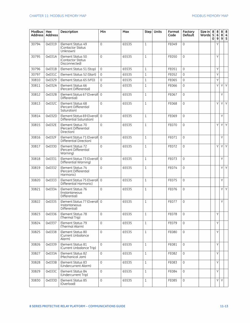
CHAPTER 11: MODBUS MEMORY MAP MODBUS MEMORY MAP
30794 0x0319 Element Status 49 (Contactor Status Unknown)
0 65535 1 FE049 0 Y
30795 0x031A Element Status 50 (Contactor Status Disconnected)
0 65535 1 FE050 0 Y
30796 0x031B Element Status 51 (Stop) 0 65535 1 FE051 0 Y
30797 0x031C Element Status 52 (Start) 0 65535 1 FE052 0 Y
30810 0x0329 Element Status 65 (VFD) 0 65535 1 FE065 0 Y
30811 0x032A Element Status 66 (Percent Differential)
0 65535 1 FE066 0 Y Y Y
30812 0x032B Element Status 67 (Overall Differential)
0 65535 1 FE067 0 Y
30813 0x032C Element Status 68 (Percent Differential Saturation)
0 65535 1 FE068 0 Y Y Y
30814 0x032D Element Status 69 (Overall Differential Saturation)
0 65535 1 FE069 0 Y
30815 0x032E Element Status 70 (Percent Differential Direction)
0 65535 1 FE070 0 Y Y Y
30816 0x032F Element Status 71 (Overall Differential Direction)
0 65535 1 FE071 0 Y
30817 0x0330 Element Status 72 (Percent Differential Warning)
0 65535 1 FE072 0 Y Y Y
30818 0x0331 Element Status 73 (Overall Differential Warning)
0 65535 1 FE073 0 Y
30819 0x0332 Element Status 74 (Percent Differential Harmonic)
0 65535 1 FE074 0 Y Y
30820 0x0333 Element Status 75 (Overall Differential Harmonic)
0 65535 1 FE075 0 Y
30821 0x0334 Element Status 76 (Instantaneous Differential)
0 65535 1 FE076 0 Y Y
30822 0x0335 Element Status 77 (Overall Instantaneous Differential)
0 65535 1 FE077 0 Y
30823 0x0336 Element Status 78 (Thermal Trip)
0 65535 1 FE078 0 Y
30824 0x0337 Element Status 79 (Thermal Alarm)
0 65535 1 FE079 0 Y
30825 0x0338 Element Status 80 (Current Unbalance Alarm)
0 65535 1 FE080 0 Y
30826 0x0339 Element Status 81 (Current Unbalance Trip)
0 65535 1 FE081 0 Y
30827 0x033A Element Status 82 (Mechanical Jam)
0 65535 1 FE082 0 Y
30828 0x033B Element Status 83 (Undercurrent Alarm)
0 65535 1 FE083 0 Y
30829 0x033C Element Status 84 (Undercurrent Trip)
0 65535 1 FE084 0 Y
30830 0x033D Element Status 85 (Overload)
0 65535 1 FE085 0 Y Y
Modbus Address
Hex Address
Description Min Max Step Units Format Code
Factory Default
Size in Words
850
869
889
845
8 SERIES PROTECTIVE RELAY PLATFORM – COMMUNICATIONS GUIDE 11-13
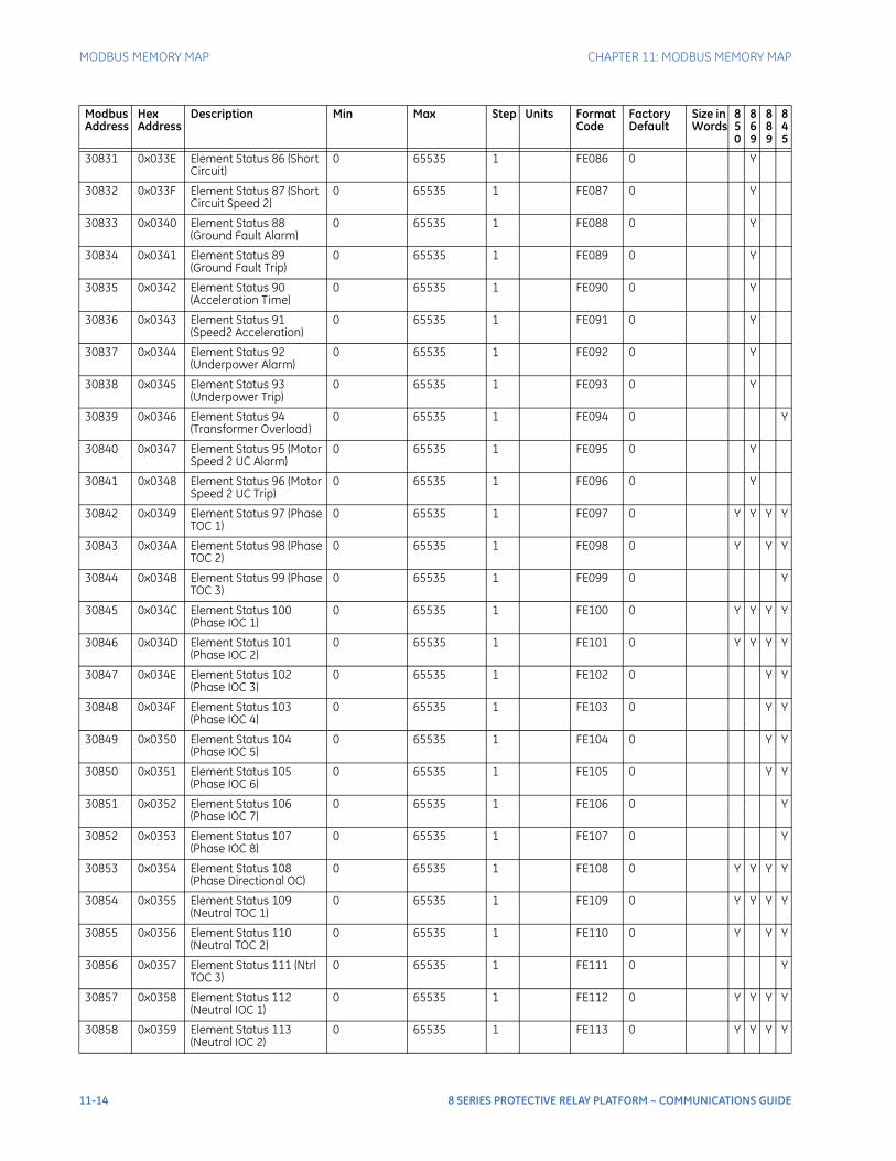
MODBUS MEMORY MAP CHAPTER 11: MODBUS MEMORY MAP
30831 0x033E Element Status 86 (Short Circuit)
0 65535 1 FE086 0 Y
30832 0x033F Element Status 87 (Short Circuit Speed 2)
0 65535 1 FE087 0 Y
30833 0x0340 Element Status 88 (Ground Fault Alarm)
0 65535 1 FE088 0 Y
30834 0x0341 Element Status 89 (Ground Fault Trip)
0 65535 1 FE089 0 Y
30835 0x0342 Element Status 90 (Acceleration Time)
0 65535 1 FE090 0 Y
30836 0x0343 Element Status 91 (Speed2 Acceleration)
0 65535 1 FE091 0 Y
30837 0x0344 Element Status 92 (Underpower Alarm)
0 65535 1 FE092 0 Y
30838 0x0345 Element Status 93 (Underpower Trip)
0 65535 1 FE093 0 Y
30839 0x0346 Element Status 94 (Transformer Overload)
0 65535 1 FE094 0 Y
30840 0x0347 Element Status 95 (Motor Speed 2 UC Alarm)
0 65535 1 FE095 0 Y
30841 0x0348 Element Status 96 (Motor Speed 2 UC Trip)
0 65535 1 FE096 0 Y
30842 0x0349 Element Status 97 (Phase TOC 1)
0 65535 1 FE097 0 Y Y Y Y
30843 0x034A Element Status 98 (Phase TOC 2)
0 65535 1 FE098 0 Y Y Y
30844 0x034B Element Status 99 (Phase TOC 3)
0 65535 1 FE099 0 Y
30845 0x034C Element Status 100 (Phase IOC 1)
0 65535 1 FE100 0 Y Y Y Y
30846 0x034D Element Status 101 (Phase IOC 2)
0 65535 1 FE101 0 Y Y Y Y
30847 0x034E Element Status 102 (Phase IOC 3)
0 65535 1 FE102 0 Y Y
30848 0x034F Element Status 103 (Phase IOC 4)
0 65535 1 FE103 0 Y Y
30849 0x0350 Element Status 104 (Phase IOC 5)
0 65535 1 FE104 0 Y Y
30850 0x0351 Element Status 105 (Phase IOC 6)
0 65535 1 FE105 0 Y Y
30851 0x0352 Element Status 106 (Phase IOC 7)
0 65535 1 FE106 0 Y
30852 0x0353 Element Status 107 (Phase IOC 8)
0 65535 1 FE107 0 Y
30853 0x0354 Element Status 108 (Phase Directional OC)
0 65535 1 FE108 0 Y Y Y Y
30854 0x0355 Element Status 109 (Neutral TOC 1)
0 65535 1 FE109 0 Y Y Y Y
30855 0x0356 Element Status 110 (Neutral TOC 2)
0 65535 1 FE110 0 Y Y Y
30856 0x0357 Element Status 111 (Ntrl TOC 3)
0 65535 1 FE111 0 Y
30857 0x0358 Element Status 112 (Neutral IOC 1)
0 65535 1 FE112 0 Y Y Y Y
30858 0x0359 Element Status 113 (Neutral IOC 2)
0 65535 1 FE113 0 Y Y Y Y
Modbus Address
Hex Address
Description Min Max Step Units Format Code
Factory Default
Size in Words
850
869
889
845
11-14 8 SERIES PROTECTIVE RELAY PLATFORM – COMMUNICATIONS GUIDE
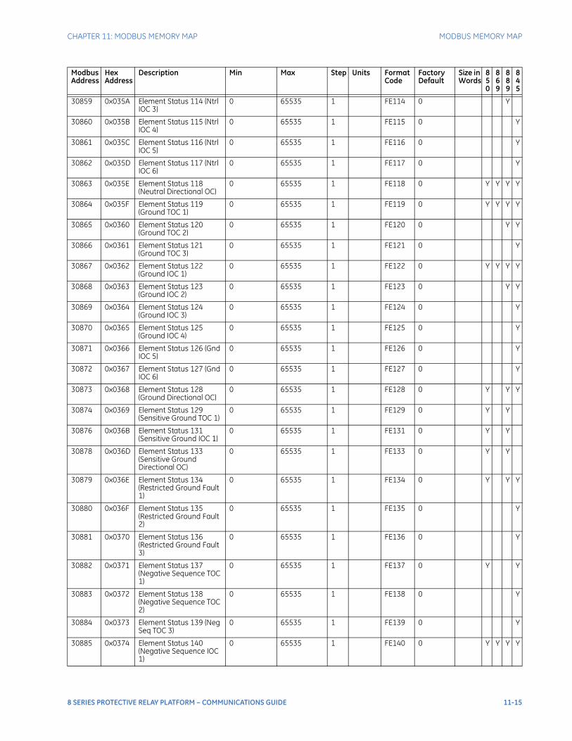
CHAPTER 11: MODBUS MEMORY MAP MODBUS MEMORY MAP
30859 0x035A Element Status 114 (Ntrl IOC 3)
0 65535 1 FE114 0 Y
30860 0x035B Element Status 115 (Ntrl IOC 4)
0 65535 1 FE115 0 Y
30861 0x035C Element Status 116 (Ntrl IOC 5)
0 65535 1 FE116 0 Y
30862 0x035D Element Status 117 (Ntrl IOC 6)
0 65535 1 FE117 0 Y
30863 0x035E Element Status 118 (Neutral Directional OC)
0 65535 1 FE118 0 Y Y Y Y
30864 0x035F Element Status 119 (Ground TOC 1)
0 65535 1 FE119 0 Y Y Y Y
30865 0x0360 Element Status 120 (Ground TOC 2)
0 65535 1 FE120 0 Y Y
30866 0x0361 Element Status 121 (Ground TOC 3)
0 65535 1 FE121 0 Y
30867 0x0362 Element Status 122 (Ground IOC 1)
0 65535 1 FE122 0 Y Y Y Y
30868 0x0363 Element Status 123 (Ground IOC 2)
0 65535 1 FE123 0 Y Y
30869 0x0364 Element Status 124 (Ground IOC 3)
0 65535 1 FE124 0 Y
30870 0x0365 Element Status 125 (Ground IOC 4)
0 65535 1 FE125 0 Y
30871 0x0366 Element Status 126 (Gnd IOC 5)
0 65535 1 FE126 0 Y
30872 0x0367 Element Status 127 (Gnd IOC 6)
0 65535 1 FE127 0 Y
30873 0x0368 Element Status 128 (Ground Directional OC)
0 65535 1 FE128 0 Y Y Y
30874 0x0369 Element Status 129 (Sensitive Ground TOC 1)
0 65535 1 FE129 0 Y Y
30876 0x036B Element Status 131 (Sensitive Ground IOC 1)
0 65535 1 FE131 0 Y Y
30878 0x036D Element Status 133 (Sensitive Ground Directional OC)
0 65535 1 FE133 0 Y Y
30879 0x036E Element Status 134 (Restricted Ground Fault 1)
0 65535 1 FE134 0 Y Y Y
30880 0x036F Element Status 135 (Restricted Ground Fault 2)
0 65535 1 FE135 0 Y
30881 0x0370 Element Status 136 (Restricted Ground Fault 3)
0 65535 1 FE136 0 Y
30882 0x0371 Element Status 137 (Negative Sequence TOC 1)
0 65535 1 FE137 0 Y Y
30883 0x0372 Element Status 138 (Negative Sequence TOC 2)
0 65535 1 FE138 0 Y
30884 0x0373 Element Status 139 (Neg Seq TOC 3)
0 65535 1 FE139 0 Y
30885 0x0374 Element Status 140 (Negative Sequence IOC 1)
0 65535 1 FE140 0 Y Y Y Y
Modbus Address
Hex Address
Description Min Max Step Units Format Code
Factory Default
Size in Words
850
869
889
845
8 SERIES PROTECTIVE RELAY PLATFORM – COMMUNICATIONS GUIDE 11-15
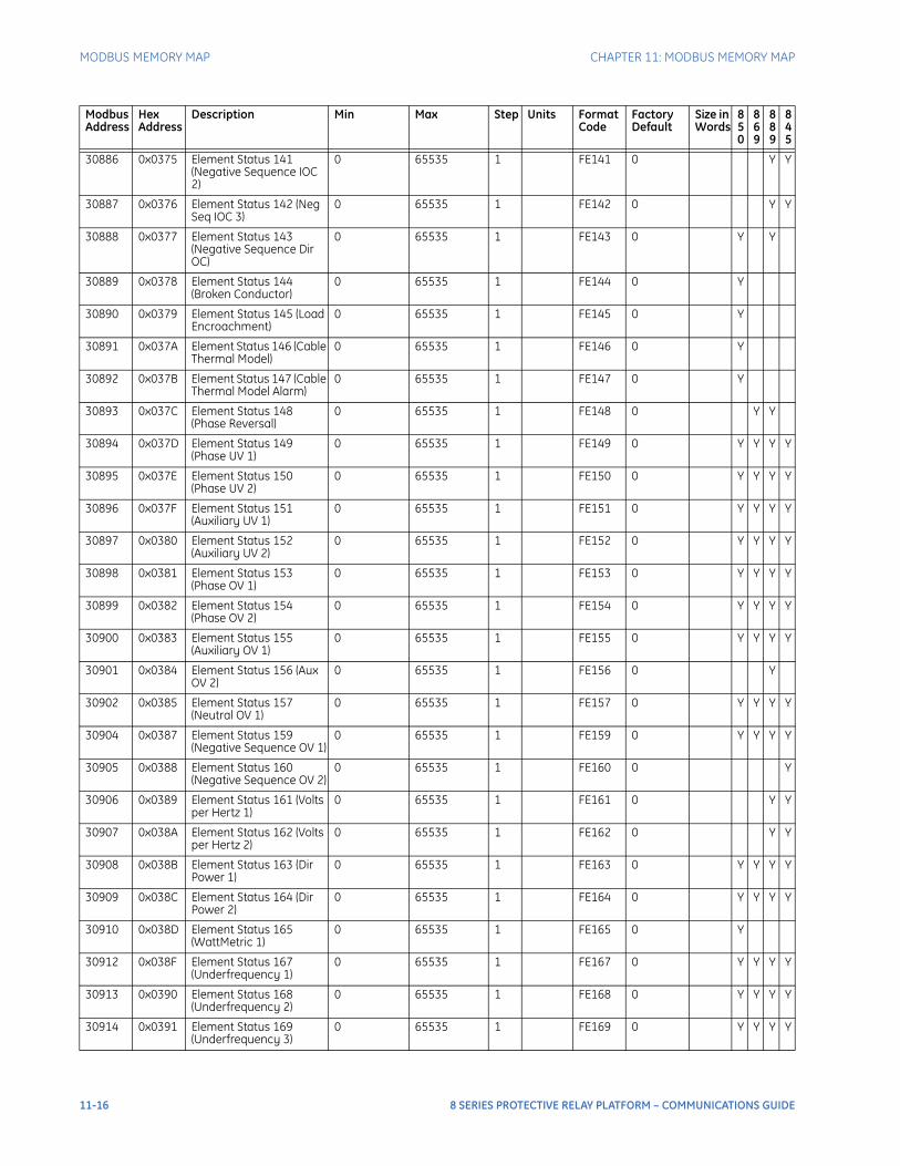
MODBUS MEMORY MAP CHAPTER 11: MODBUS MEMORY MAP
30886 0x0375 Element Status 141 (Negative Sequence IOC 2)
0 65535 1 FE141 0 Y Y
30887 0x0376 Element Status 142 (Neg Seq IOC 3)
0 65535 1 FE142 0 Y Y
30888 0x0377 Element Status 143 (Negative Sequence Dir OC)
0 65535 1 FE143 0 Y Y
30889 0x0378 Element Status 144 (Broken Conductor)
0 65535 1 FE144 0 Y
30890 0x0379 Element Status 145 (Load Encroachment)
0 65535 1 FE145 0 Y
30891 0x037A Element Status 146 (Cable Thermal Model)
0 65535 1 FE146 0 Y
30892 0x037B Element Status 147 (Cable Thermal Model Alarm)
0 65535 1 FE147 0 Y
30893 0x037C Element Status 148 (Phase Reversal)
0 65535 1 FE148 0 Y Y
30894 0x037D Element Status 149 (Phase UV 1)
0 65535 1 FE149 0 Y Y Y Y
30895 0x037E Element Status 150 (Phase UV 2)
0 65535 1 FE150 0 Y Y Y Y
30896 0x037F Element Status 151 (Auxiliary UV 1)
0 65535 1 FE151 0 Y Y Y Y
30897 0x0380 Element Status 152 (Auxiliary UV 2)
0 65535 1 FE152 0 Y Y Y Y
30898 0x0381 Element Status 153 (Phase OV 1)
0 65535 1 FE153 0 Y Y Y Y
30899 0x0382 Element Status 154 (Phase OV 2)
0 65535 1 FE154 0 Y Y Y Y
30900 0x0383 Element Status 155 (Auxiliary OV 1)
0 65535 1 FE155 0 Y Y Y Y
30901 0x0384 Element Status 156 (Aux OV 2)
0 65535 1 FE156 0 Y
30902 0x0385 Element Status 157 (Neutral OV 1)
0 65535 1 FE157 0 Y Y Y Y
30904 0x0387 Element Status 159 (Negative Sequence OV 1)
0 65535 1 FE159 0 Y Y Y Y
30905 0x0388 Element Status 160 (Negative Sequence OV 2)
0 65535 1 FE160 0 Y
30906 0x0389 Element Status 161 (Volts per Hertz 1)
0 65535 1 FE161 0 Y Y
30907 0x038A Element Status 162 (Volts per Hertz 2)
0 65535 1 FE162 0 Y Y
30908 0x038B Element Status 163 (Dir Power 1)
0 65535 1 FE163 0 Y Y Y Y
30909 0x038C Element Status 164 (Dir Power 2)
0 65535 1 FE164 0 Y Y Y Y
30910 0x038D Element Status 165 (WattMetric 1)
0 65535 1 FE165 0 Y
30912 0x038F Element Status 167 (Underfrequency 1)
0 65535 1 FE167 0 Y Y Y Y
30913 0x0390 Element Status 168 (Underfrequency 2)
0 65535 1 FE168 0 Y Y Y Y
30914 0x0391 Element Status 169 (Underfrequency 3)
0 65535 1 FE169 0 Y Y Y Y
Modbus Address
Hex Address
Description Min Max Step Units Format Code
Factory Default
Size in Words
850
869
889
845
11-16 8 SERIES PROTECTIVE RELAY PLATFORM – COMMUNICATIONS GUIDE
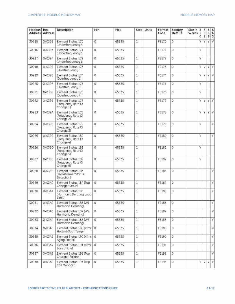
CHAPTER 11: MODBUS MEMORY MAP MODBUS MEMORY MAP
30915 0x0392 Element Status 170 (Underfrequency 4)
0 65535 1 FE170 0 Y Y Y Y
30916 0x0393 Element Status 171 (Underfrequency 5)
0 65535 1 FE171 0 Y
30917 0x0394 Element Status 172 (Underfrequency 6)
0 65535 1 FE172 0 Y
30918 0x0395 Element Status 173 (Overfrequency 1)
0 65535 1 FE173 0 Y Y Y Y
30919 0x0396 Element Status 174 (Overfrequency 2)
0 65535 1 FE174 0 Y Y Y Y
30920 0x0397 Element Status 175 (Overfrequency 3)
0 65535 1 FE175 0 Y
30921 0x0398 Element Status 176 (Overfrequency 4)
0 65535 1 FE176 0 Y
30922 0x0399 Element Status 177 (Frequency Rate Of Change 1)
0 65535 1 FE177 0 Y Y Y Y
30923 0x039A Element Status 178 (Frequency Rate Of Change 2)
0 65535 1 FE178 0 Y Y Y Y
30924 0x039B Element Status 179 (Frequency Rate Of Change 3)
0 65535 1 FE179 0 Y Y
30925 0x039C Element Status 180 (Frequency Rate Of Change 4)
0 65535 1 FE180 0 Y Y
30926 0x039D Element Status 181 (Frequency Rate Of Change 5)
0 65535 1 FE181 0 Y
30927 0x039E Element Status 182 (Frequency Rate Of Change 6)
0 65535 1 FE182 0 Y
30928 0x039F Element Status 183 (Transformer Status Detection)
0 65535 1 FE183 0 Y
30929 0x03A0 Element Status 184 (Tap Changer Setup)
0 65535 1 FE184 0 Y
30930 0x03A1 Element Status 185 (Harmonic Derating Load Limit)
0 65535 1 FE185 0 Y
30931 0x03A2 Element Status 186 (W1 Harmonic Derating)
0 65535 1 FE186 0 Y
30932 0x03A3 Element Status 187 (W2 Harmonic Derating)
0 65535 1 FE187 0 Y
30933 0x03A4 Element Status 188 (W3 Harmonic Derating)
0 65535 1 FE188 0 Y
30934 0x03A5 Element Status 189 (Xfmr Hottest-Spot Temp)
0 65535 1 FE189 0 Y
30935 0x03A6 Element Status 190 (Xfmr Aging Factor)
0 65535 1 FE190 0 Y
30936 0x03A7 Element Status 191 (Xfmr Loss of Life)
0 65535 1 FE191 0 Y
30937 0x03A8 Element Status 192 (Tap Changer Failure)
0 65535 1 FE192 0 Y
30938 0x03A9 Element Status 193 (Trip Coil Monitor 1)
0 65535 1 FE193 0 Y Y Y Y
Modbus Address
Hex Address
Description Min Max Step Units Format Code
Factory Default
Size in Words
850
869
889
845
8 SERIES PROTECTIVE RELAY PLATFORM – COMMUNICATIONS GUIDE 11-17
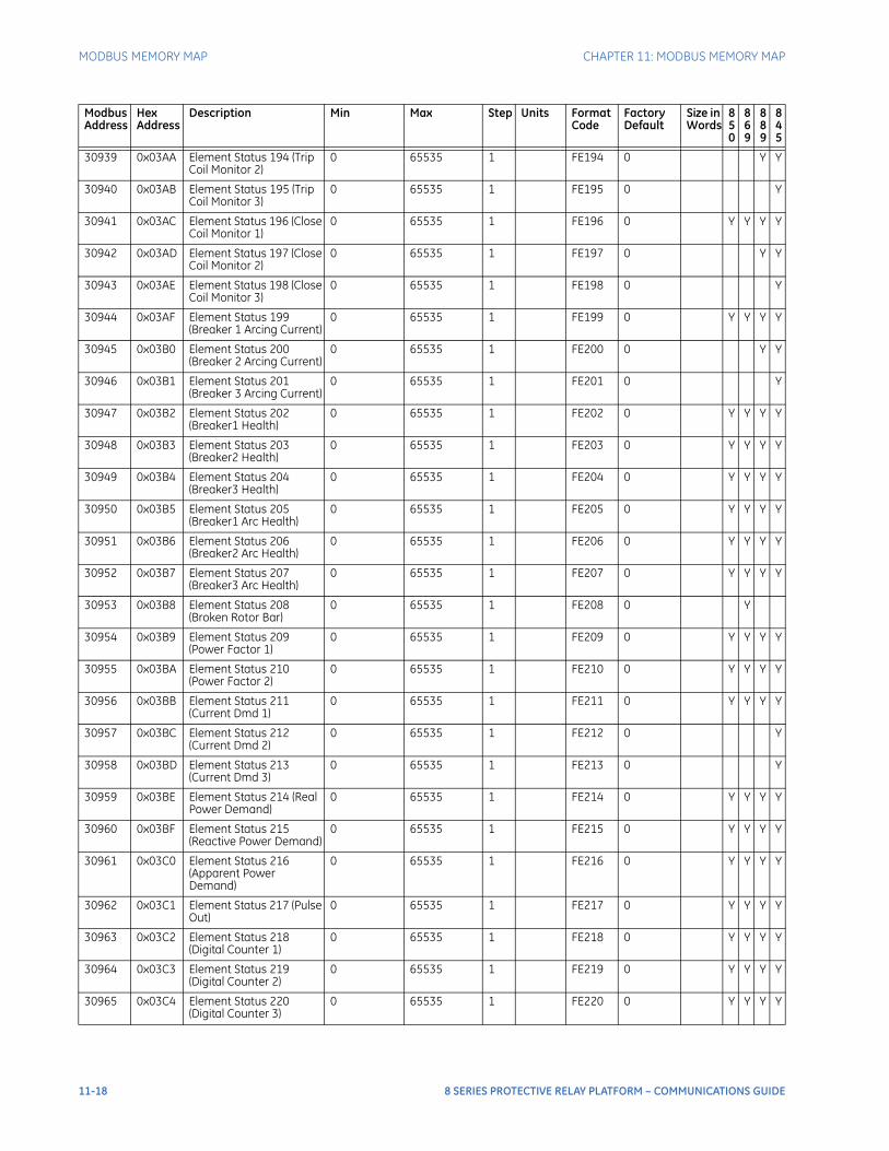
MODBUS MEMORY MAP CHAPTER 11: MODBUS MEMORY MAP
30939 0x03AA Element Status 194 (Trip Coil Monitor 2)
0 65535 1 FE194 0 Y Y
30940 0x03AB Element Status 195 (Trip Coil Monitor 3)
0 65535 1 FE195 0 Y
30941 0x03AC Element Status 196 (Close Coil Monitor 1)
0 65535 1 FE196 0 Y Y Y Y
30942 0x03AD Element Status 197 (Close Coil Monitor 2)
0 65535 1 FE197 0 Y Y
30943 0x03AE Element Status 198 (Close Coil Monitor 3)
0 65535 1 FE198 0 Y
30944 0x03AF Element Status 199 (Breaker 1 Arcing Current)
0 65535 1 FE199 0 Y Y Y Y
30945 0x03B0 Element Status 200 (Breaker 2 Arcing Current)
0 65535 1 FE200 0 Y Y
30946 0x03B1 Element Status 201 (Breaker 3 Arcing Current)
0 65535 1 FE201 0 Y
30947 0x03B2 Element Status 202 (Breaker1 Health)
0 65535 1 FE202 0 Y Y Y Y
30948 0x03B3 Element Status 203 (Breaker2 Health)
0 65535 1 FE203 0 Y Y Y Y
30949 0x03B4 Element Status 204 (Breaker3 Health)
0 65535 1 FE204 0 Y Y Y Y
30950 0x03B5 Element Status 205 (Breaker1 Arc Health)
0 65535 1 FE205 0 Y Y Y Y
30951 0x03B6 Element Status 206 (Breaker2 Arc Health)
0 65535 1 FE206 0 Y Y Y Y
30952 0x03B7 Element Status 207 (Breaker3 Arc Health)
0 65535 1 FE207 0 Y Y Y Y
30953 0x03B8 Element Status 208 (Broken Rotor Bar)
0 65535 1 FE208 0 Y
30954 0x03B9 Element Status 209 (Power Factor 1)
0 65535 1 FE209 0 Y Y Y Y
30955 0x03BA Element Status 210 (Power Factor 2)
0 65535 1 FE210 0 Y Y Y Y
30956 0x03BB Element Status 211 (Current Dmd 1)
0 65535 1 FE211 0 Y Y Y Y
30957 0x03BC Element Status 212 (Current Dmd 2)
0 65535 1 FE212 0 Y
30958 0x03BD Element Status 213 (Current Dmd 3)
0 65535 1 FE213 0 Y
30959 0x03BE Element Status 214 (Real Power Demand)
0 65535 1 FE214 0 Y Y Y Y
30960 0x03BF Element Status 215 (Reactive Power Demand)
0 65535 1 FE215 0 Y Y Y Y
30961 0x03C0 Element Status 216 (Apparent Power Demand)
0 65535 1 FE216 0 Y Y Y Y
30962 0x03C1 Element Status 217 (Pulse Out)
0 65535 1 FE217 0 Y Y Y Y
30963 0x03C2 Element Status 218 (Digital Counter 1)
0 65535 1 FE218 0 Y Y Y Y
30964 0x03C3 Element Status 219 (Digital Counter 2)
0 65535 1 FE219 0 Y Y Y Y
30965 0x03C4 Element Status 220 (Digital Counter 3)
0 65535 1 FE220 0 Y Y Y Y
Modbus Address
Hex Address
Description Min Max Step Units Format Code
Factory Default
Size in Words
850
869
889
845
11-18 8 SERIES PROTECTIVE RELAY PLATFORM – COMMUNICATIONS GUIDE
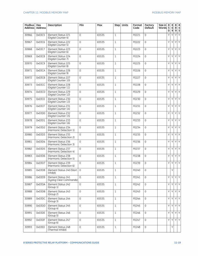
CHAPTER 11: MODBUS MEMORY MAP MODBUS MEMORY MAP
30966 0x03C5 Element Status 221 (Digital Counter 4)
0 65535 1 FE221 0 Y Y Y Y
30967 0x03C6 Element Status 222 (Digital Counter 5)
0 65535 1 FE222 0 Y Y Y Y
30968 0x03C7 Element Status 223 (Digital Counter 6)
0 65535 1 FE223 0 Y Y Y Y
30969 0x03C8 Element Status 224 (Digital Counter 7)
0 65535 1 FE224 0 Y Y Y Y
30970 0x03C9 Element Status 225 (Digital Counter 8)
0 65535 1 FE225 0 Y Y Y Y
30971 0x03CA Element Status 226 (Digital Counter 9)
0 65535 1 FE226 0 Y Y Y Y
30972 0x03CB Element Status 227 (Digital Counter 10)
0 65535 1 FE227 0 Y Y Y Y
30973 0x03CC Element Status 228 (Digital Counter 11)
0 65535 1 FE228 0 Y Y Y Y
30974 0x03CD Element Status 229 (Digital Counter 12)
0 65535 1 FE229 0 Y Y Y Y
30975 0x03CE Element Status 230 (Digital Counter 13)
0 65535 1 FE230 0 Y Y Y Y
30976 0x03CF Element Status 231 (Digital Counter 14)
0 65535 1 FE231 0 Y Y Y Y
30977 0x03D0 Element Status 232 (Digital Counter 15)
0 65535 1 FE232 0 Y Y Y Y
30978 0x03D1 Element Status 233 (Digital Counter 16)
0 65535 1 FE233 0 Y Y Y Y
30979 0x03D2 Element Status 234 (Harmonic Detection 1)
0 65535 1 FE234 0 Y Y Y Y
30980 0x03D3 Element Status 235 (Harmonic Detection 2)
0 65535 1 FE235 0 Y Y Y Y
30981 0x03D4 Element Status 236 (Harmonic Detection 3)
0 65535 1 FE236 0 Y Y Y Y
30982 0x03D5 Element Status 237 (Harmonic Detection 4)
0 65535 1 FE237 0 Y Y Y Y
30983 0x03D6 Element Status 238 (Harmonic Detection 5)
0 65535 1 FE238 0 Y Y Y Y
30984 0x03D7 Element Status 239 (Harmonic Detection 6)
0 65535 1 FE239 0 Y Y Y Y
30985 0x03D8 Element Status 240 (Start Inhibit)
0 65535 1 FE240 0 Y
30986 0x03D9 Element Status 241 (Syslog Clear Commands)
0 65535 1 FE241 0 Y Y Y Y
30987 0x03DA Element Status 242 (Group 1)
0 65535 1 FE242 0 Y Y Y Y
30988 0x03DB Element Status 243 (Group 2)
0 65535 1 FE243 0 Y Y Y Y
30989 0x03DC Element Status 244 (Group 3)
0 65535 1 FE244 0 Y Y Y Y
30990 0x03DD Element Status 245 (Group 4)
0 65535 1 FE245 0 Y Y Y Y
30991 0x03DE Element Status 246 (Group 5)
0 65535 1 FE246 0 Y Y Y Y
30992 0x03DF Element Status 247 (Group 6)
0 65535 1 FE247 0 Y Y Y Y
30993 0x03E0 Element Status 248 (Thermal Inhibit)
0 65535 1 FE248 0 Y
Modbus Address
Hex Address
Description Min Max Step Units Format Code
Factory Default
Size in Words
850
869
889
845
8 SERIES PROTECTIVE RELAY PLATFORM – COMMUNICATIONS GUIDE 11-19
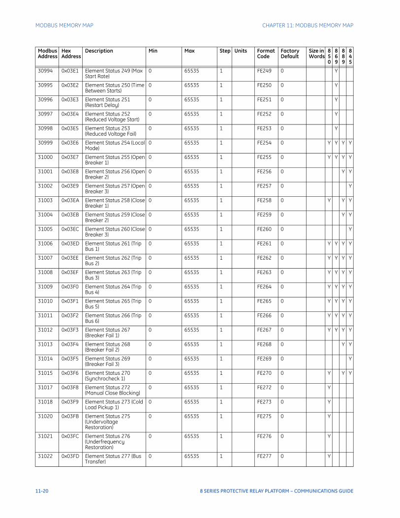
MODBUS MEMORY MAP CHAPTER 11: MODBUS MEMORY MAP
30994 0x03E1 Element Status 249 (Max Start Rate)
0 65535 1 FE249 0 Y
30995 0x03E2 Element Status 250 (Time Between Starts)
0 65535 1 FE250 0 Y
30996 0x03E3 Element Status 251 (Restart Delay)
0 65535 1 FE251 0 Y
30997 0x03E4 Element Status 252 (Reduced Voltage Start)
0 65535 1 FE252 0 Y
30998 0x03E5 Element Status 253 (Reduced Voltage Fail)
0 65535 1 FE253 0 Y
30999 0x03E6 Element Status 254 (Local Mode)
0 65535 1 FE254 0 Y Y Y Y
31000 0x03E7 Element Status 255 (Open Breaker 1)
0 65535 1 FE255 0 Y Y Y Y
31001 0x03E8 Element Status 256 (Open Breaker 2)
0 65535 1 FE256 0 Y Y
31002 0x03E9 Element Status 257 (Open Breaker 3)
0 65535 1 FE257 0 Y
31003 0x03EA Element Status 258 (Close Breaker 1)
0 65535 1 FE258 0 Y Y Y
31004 0x03EB Element Status 259 (Close Breaker 2)
0 65535 1 FE259 0 Y Y
31005 0x03EC Element Status 260 (Close Breaker 3)
0 65535 1 FE260 0 Y
31006 0x03ED Element Status 261 (Trip Bus 1)
0 65535 1 FE261 0 Y Y Y Y
31007 0x03EE Element Status 262 (Trip Bus 2)
0 65535 1 FE262 0 Y Y Y Y
31008 0x03EF Element Status 263 (Trip Bus 3)
0 65535 1 FE263 0 Y Y Y Y
31009 0x03F0 Element Status 264 (Trip Bus 4)
0 65535 1 FE264 0 Y Y Y Y
31010 0x03F1 Element Status 265 (Trip Bus 5)
0 65535 1 FE265 0 Y Y Y Y
31011 0x03F2 Element Status 266 (Trip Bus 6)
0 65535 1 FE266 0 Y Y Y Y
31012 0x03F3 Element Status 267 (Breaker Fail 1)
0 65535 1 FE267 0 Y Y Y Y
31013 0x03F4 Element Status 268 (Breaker Fail 2)
0 65535 1 FE268 0 Y Y
31014 0x03F5 Element Status 269 (Breaker Fail 3)
0 65535 1 FE269 0 Y
31015 0x03F6 Element Status 270 (Synchrocheck 1)
0 65535 1 FE270 0 Y Y Y
31017 0x03F8 Element Status 272 (Manual Close Blocking)
0 65535 1 FE272 0 Y
31018 0x03F9 Element Status 273 (Cold Load Pickup 1)
0 65535 1 FE273 0 Y
31020 0x03FB Element Status 275 (Undervoltage Restoration)
0 65535 1 FE275 0 Y
31021 0x03FC Element Status 276 (Underfrequency Restoration)
0 65535 1 FE276 0 Y
31022 0x03FD Element Status 277 (Bus Transfer)
0 65535 1 FE277 0 Y
Modbus Address
Hex Address
Description Min Max Step Units Format Code
Factory Default
Size in Words
850
869
889
845
11-20 8 SERIES PROTECTIVE RELAY PLATFORM – COMMUNICATIONS GUIDE
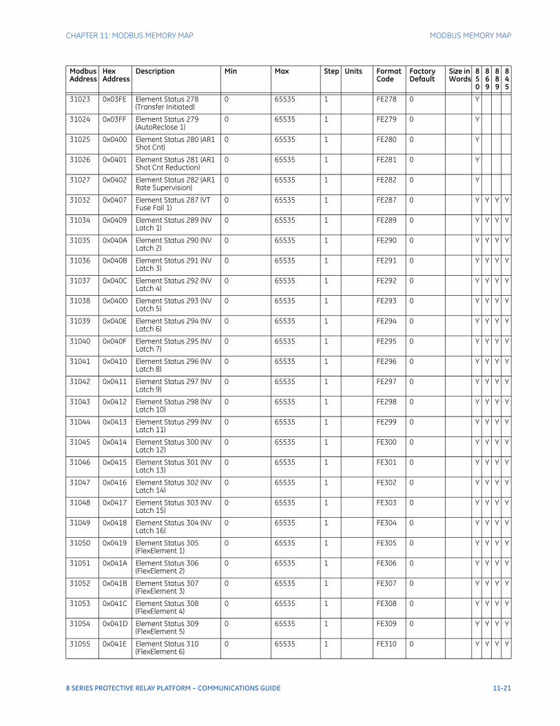
CHAPTER 11: MODBUS MEMORY MAP MODBUS MEMORY MAP
31023 0x03FE Element Status 278 (Transfer Initiated)
0 65535 1 FE278 0 Y
31024 0x03FF Element Status 279 (AutoReclose 1)
0 65535 1 FE279 0 Y
31025 0x0400 Element Status 280 (AR1 Shot Cnt)
0 65535 1 FE280 0 Y
31026 0x0401 Element Status 281 (AR1 Shot Cnt Reduction)
0 65535 1 FE281 0 Y
31027 0x0402 Element Status 282 (AR1 Rate Supervision)
0 65535 1 FE282 0 Y
31032 0x0407 Element Status 287 (VT Fuse Fail 1)
0 65535 1 FE287 0 Y Y Y Y
31034 0x0409 Element Status 289 (NV Latch 1)
0 65535 1 FE289 0 Y Y Y Y
31035 0x040A Element Status 290 (NV Latch 2)
0 65535 1 FE290 0 Y Y Y Y
31036 0x040B Element Status 291 (NV Latch 3)
0 65535 1 FE291 0 Y Y Y Y
31037 0x040C Element Status 292 (NV Latch 4)
0 65535 1 FE292 0 Y Y Y Y
31038 0x040D Element Status 293 (NV Latch 5)
0 65535 1 FE293 0 Y Y Y Y
31039 0x040E Element Status 294 (NV Latch 6)
0 65535 1 FE294 0 Y Y Y Y
31040 0x040F Element Status 295 (NV Latch 7)
0 65535 1 FE295 0 Y Y Y Y
31041 0x0410 Element Status 296 (NV Latch 8)
0 65535 1 FE296 0 Y Y Y Y
31042 0x0411 Element Status 297 (NV Latch 9)
0 65535 1 FE297 0 Y Y Y Y
31043 0x0412 Element Status 298 (NV Latch 10)
0 65535 1 FE298 0 Y Y Y Y
31044 0x0413 Element Status 299 (NV Latch 11)
0 65535 1 FE299 0 Y Y Y Y
31045 0x0414 Element Status 300 (NV Latch 12)
0 65535 1 FE300 0 Y Y Y Y
31046 0x0415 Element Status 301 (NV Latch 13)
0 65535 1 FE301 0 Y Y Y Y
31047 0x0416 Element Status 302 (NV Latch 14)
0 65535 1 FE302 0 Y Y Y Y
31048 0x0417 Element Status 303 (NV Latch 15)
0 65535 1 FE303 0 Y Y Y Y
31049 0x0418 Element Status 304 (NV Latch 16)
0 65535 1 FE304 0 Y Y Y Y
31050 0x0419 Element Status 305 (FlexElement 1)
0 65535 1 FE305 0 Y Y Y Y
31051 0x041A Element Status 306 (FlexElement 2)
0 65535 1 FE306 0 Y Y Y Y
31052 0x041B Element Status 307 (FlexElement 3)
0 65535 1 FE307 0 Y Y Y Y
31053 0x041C Element Status 308 (FlexElement 4)
0 65535 1 FE308 0 Y Y Y Y
31054 0x041D Element Status 309 (FlexElement 5)
0 65535 1 FE309 0 Y Y Y Y
31055 0x041E Element Status 310 (FlexElement 6)
0 65535 1 FE310 0 Y Y Y Y
Modbus Address
Hex Address
Description Min Max Step Units Format Code
Factory Default
Size in Words
850
869
889
845
8 SERIES PROTECTIVE RELAY PLATFORM – COMMUNICATIONS GUIDE 11-21
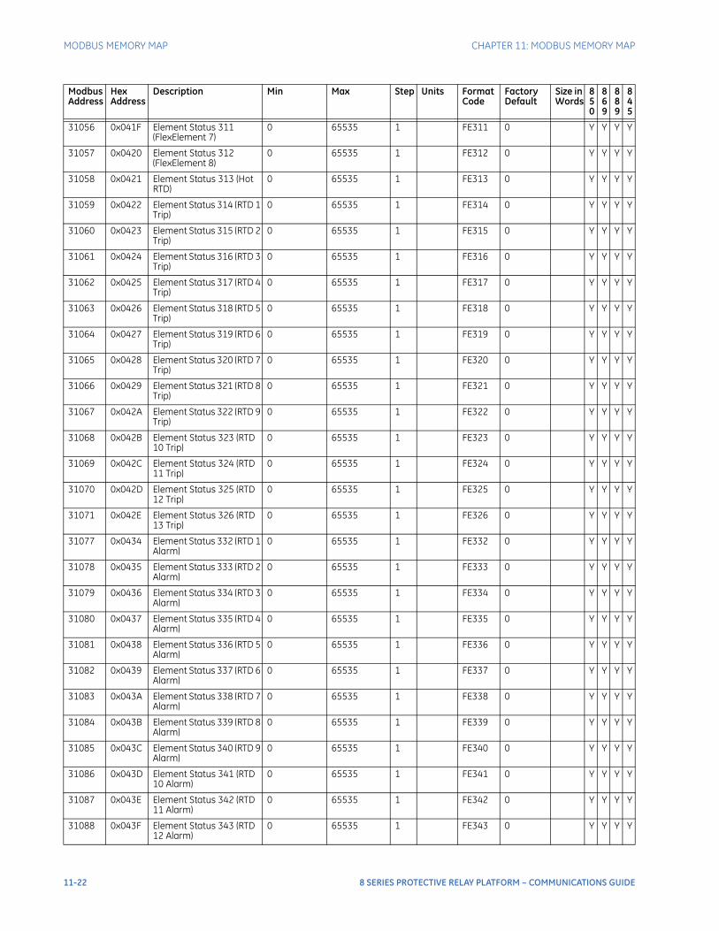
MODBUS MEMORY MAP CHAPTER 11: MODBUS MEMORY MAP
31056 0x041F Element Status 311 (FlexElement 7)
0 65535 1 FE311 0 Y Y Y Y
31057 0x0420 Element Status 312 (FlexElement 8)
0 65535 1 FE312 0 Y Y Y Y
31058 0x0421 Element Status 313 (Hot RTD)
0 65535 1 FE313 0 Y Y Y Y
31059 0x0422 Element Status 314 (RTD 1 Trip)
0 65535 1 FE314 0 Y Y Y Y
31060 0x0423 Element Status 315 (RTD 2 Trip)
0 65535 1 FE315 0 Y Y Y Y
31061 0x0424 Element Status 316 (RTD 3 Trip)
0 65535 1 FE316 0 Y Y Y Y
31062 0x0425 Element Status 317 (RTD 4 Trip)
0 65535 1 FE317 0 Y Y Y Y
31063 0x0426 Element Status 318 (RTD 5 Trip)
0 65535 1 FE318 0 Y Y Y Y
31064 0x0427 Element Status 319 (RTD 6 Trip)
0 65535 1 FE319 0 Y Y Y Y
31065 0x0428 Element Status 320 (RTD 7 Trip)
0 65535 1 FE320 0 Y Y Y Y
31066 0x0429 Element Status 321 (RTD 8 Trip)
0 65535 1 FE321 0 Y Y Y Y
31067 0x042A Element Status 322 (RTD 9 Trip)
0 65535 1 FE322 0 Y Y Y Y
31068 0x042B Element Status 323 (RTD 10 Trip)
0 65535 1 FE323 0 Y Y Y Y
31069 0x042C Element Status 324 (RTD 11 Trip)
0 65535 1 FE324 0 Y Y Y Y
31070 0x042D Element Status 325 (RTD 12 Trip)
0 65535 1 FE325 0 Y Y Y Y
31071 0x042E Element Status 326 (RTD 13 Trip)
0 65535 1 FE326 0 Y Y Y Y
31077 0x0434 Element Status 332 (RTD 1 Alarm)
0 65535 1 FE332 0 Y Y Y Y
31078 0x0435 Element Status 333 (RTD 2 Alarm)
0 65535 1 FE333 0 Y Y Y Y
31079 0x0436 Element Status 334 (RTD 3 Alarm)
0 65535 1 FE334 0 Y Y Y Y
31080 0x0437 Element Status 335 (RTD 4 Alarm)
0 65535 1 FE335 0 Y Y Y Y
31081 0x0438 Element Status 336 (RTD 5 Alarm)
0 65535 1 FE336 0 Y Y Y Y
31082 0x0439 Element Status 337 (RTD 6 Alarm)
0 65535 1 FE337 0 Y Y Y Y
31083 0x043A Element Status 338 (RTD 7 Alarm)
0 65535 1 FE338 0 Y Y Y Y
31084 0x043B Element Status 339 (RTD 8 Alarm)
0 65535 1 FE339 0 Y Y Y Y
31085 0x043C Element Status 340 (RTD 9 Alarm)
0 65535 1 FE340 0 Y Y Y Y
31086 0x043D Element Status 341 (RTD 10 Alarm)
0 65535 1 FE341 0 Y Y Y Y
31087 0x043E Element Status 342 (RTD 11 Alarm)
0 65535 1 FE342 0 Y Y Y Y
31088 0x043F Element Status 343 (RTD 12 Alarm)
0 65535 1 FE343 0 Y Y Y Y
Modbus Address
Hex Address
Description Min Max Step Units Format Code
Factory Default
Size in Words
850
869
889
845
11-22 8 SERIES PROTECTIVE RELAY PLATFORM – COMMUNICATIONS GUIDE
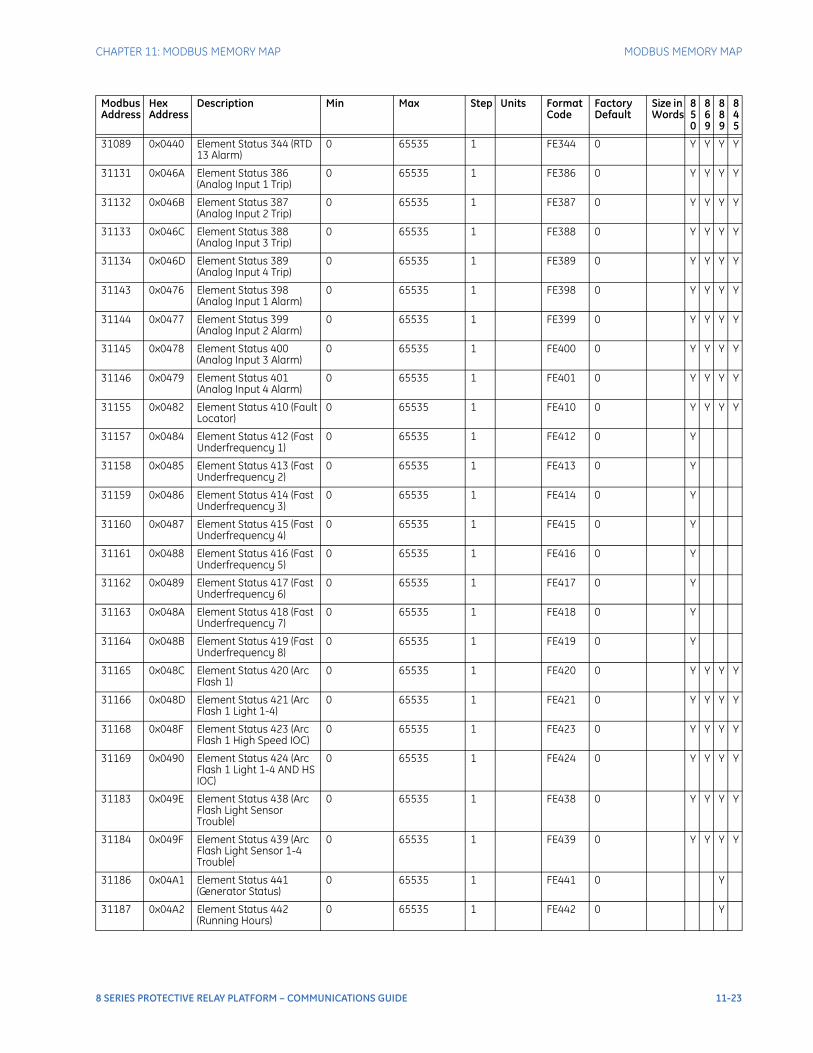
CHAPTER 11: MODBUS MEMORY MAP MODBUS MEMORY MAP
31089 0x0440 Element Status 344 (RTD 13 Alarm)
0 65535 1 FE344 0 Y Y Y Y
31131 0x046A Element Status 386 (Analog Input 1 Trip)
0 65535 1 FE386 0 Y Y Y Y
31132 0x046B Element Status 387 (Analog Input 2 Trip)
0 65535 1 FE387 0 Y Y Y Y
31133 0x046C Element Status 388 (Analog Input 3 Trip)
0 65535 1 FE388 0 Y Y Y Y
31134 0x046D Element Status 389 (Analog Input 4 Trip)
0 65535 1 FE389 0 Y Y Y Y
31143 0x0476 Element Status 398 (Analog Input 1 Alarm)
0 65535 1 FE398 0 Y Y Y Y
31144 0x0477 Element Status 399 (Analog Input 2 Alarm)
0 65535 1 FE399 0 Y Y Y Y
31145 0x0478 Element Status 400 (Analog Input 3 Alarm)
0 65535 1 FE400 0 Y Y Y Y
31146 0x0479 Element Status 401 (Analog Input 4 Alarm)
0 65535 1 FE401 0 Y Y Y Y
31155 0x0482 Element Status 410 (Fault Locator)
0 65535 1 FE410 0 Y Y Y Y
31157 0x0484 Element Status 412 (Fast Underfrequency 1)
0 65535 1 FE412 0 Y
31158 0x0485 Element Status 413 (Fast Underfrequency 2)
0 65535 1 FE413 0 Y
31159 0x0486 Element Status 414 (Fast Underfrequency 3)
0 65535 1 FE414 0 Y
31160 0x0487 Element Status 415 (Fast Underfrequency 4)
0 65535 1 FE415 0 Y
31161 0x0488 Element Status 416 (Fast Underfrequency 5)
0 65535 1 FE416 0 Y
31162 0x0489 Element Status 417 (Fast Underfrequency 6)
0 65535 1 FE417 0 Y
31163 0x048A Element Status 418 (Fast Underfrequency 7)
0 65535 1 FE418 0 Y
31164 0x048B Element Status 419 (Fast Underfrequency 8)
0 65535 1 FE419 0 Y
31165 0x048C Element Status 420 (Arc Flash 1)
0 65535 1 FE420 0 Y Y Y Y
31166 0x048D Element Status 421 (Arc Flash 1 Light 1-4)
0 65535 1 FE421 0 Y Y Y Y
31168 0x048F Element Status 423 (Arc Flash 1 High Speed IOC)
0 65535 1 FE423 0 Y Y Y Y
31169 0x0490 Element Status 424 (Arc Flash 1 Light 1-4 AND HS IOC)
0 65535 1 FE424 0 Y Y Y Y
31183 0x049E Element Status 438 (Arc Flash Light Sensor Trouble)
0 65535 1 FE438 0 Y Y Y Y
31184 0x049F Element Status 439 (Arc Flash Light Sensor 1-4 Trouble)
0 65535 1 FE439 0 Y Y Y Y
31186 0x04A1 Element Status 441 (Generator Status)
0 65535 1 FE441 0 Y
31187 0x04A2 Element Status 442 (Running Hours)
0 65535 1 FE442 0 Y
Modbus Address
Hex Address
Description Min Max Step Units Format Code
Factory Default
Size in Words
850
869
889
845
8 SERIES PROTECTIVE RELAY PLATFORM – COMMUNICATIONS GUIDE 11-23
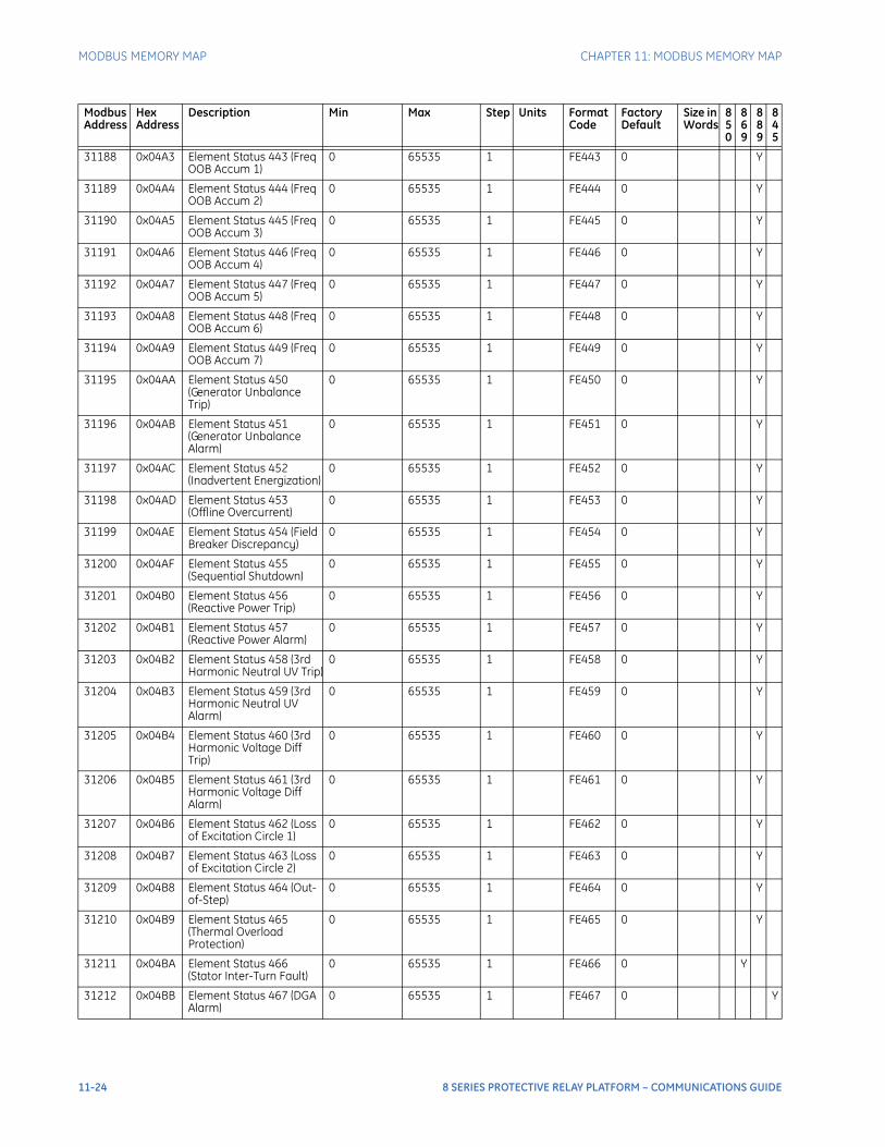
MODBUS MEMORY MAP CHAPTER 11: MODBUS MEMORY MAP
31188 0x04A3 Element Status 443 (Freq OOB Accum 1)
0 65535 1 FE443 0 Y
31189 0x04A4 Element Status 444 (Freq OOB Accum 2)
0 65535 1 FE444 0 Y
31190 0x04A5 Element Status 445 (Freq OOB Accum 3)
0 65535 1 FE445 0 Y
31191 0x04A6 Element Status 446 (Freq OOB Accum 4)
0 65535 1 FE446 0 Y
31192 0x04A7 Element Status 447 (Freq OOB Accum 5)
0 65535 1 FE447 0 Y
31193 0x04A8 Element Status 448 (Freq OOB Accum 6)
0 65535 1 FE448 0 Y
31194 0x04A9 Element Status 449 (Freq OOB Accum 7)
0 65535 1 FE449 0 Y
31195 0x04AA Element Status 450 (Generator Unbalance Trip)
0 65535 1 FE450 0 Y
31196 0x04AB Element Status 451 (Generator Unbalance Alarm)
0 65535 1 FE451 0 Y
31197 0x04AC Element Status 452 (Inadvertent Energization)
0 65535 1 FE452 0 Y
31198 0x04AD Element Status 453 (Offline Overcurrent)
0 65535 1 FE453 0 Y
31199 0x04AE Element Status 454 (Field Breaker Discrepancy)
0 65535 1 FE454 0 Y
31200 0x04AF Element Status 455 (Sequential Shutdown)
0 65535 1 FE455 0 Y
31201 0x04B0 Element Status 456 (Reactive Power Trip)
0 65535 1 FE456 0 Y
31202 0x04B1 Element Status 457 (Reactive Power Alarm)
0 65535 1 FE457 0 Y
31203 0x04B2 Element Status 458 (3rd Harmonic Neutral UV Trip)
0 65535 1 FE458 0 Y
31204 0x04B3 Element Status 459 (3rd Harmonic Neutral UV Alarm)
0 65535 1 FE459 0 Y
31205 0x04B4 Element Status 460 (3rd Harmonic Voltage Diff Trip)
0 65535 1 FE460 0 Y
31206 0x04B5 Element Status 461 (3rd Harmonic Voltage Diff Alarm)
0 65535 1 FE461 0 Y
31207 0x04B6 Element Status 462 (Loss of Excitation Circle 1)
0 65535 1 FE462 0 Y
31208 0x04B7 Element Status 463 (Loss of Excitation Circle 2)
0 65535 1 FE463 0 Y
31209 0x04B8 Element Status 464 (Out-of-Step)
0 65535 1 FE464 0 Y
31210 0x04B9 Element Status 465 (Thermal Overload Protection)
0 65535 1 FE465 0 Y
31211 0x04BA Element Status 466 (Stator Inter-Turn Fault)
0 65535 1 FE466 0 Y
31212 0x04BB Element Status 467 (DGA Alarm)
0 65535 1 FE467 0 Y
Modbus Address
Hex Address
Description Min Max Step Units Format Code
Factory Default
Size in Words
850
869
889
845
11-24 8 SERIES PROTECTIVE RELAY PLATFORM – COMMUNICATIONS GUIDE
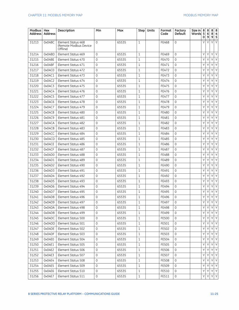
CHAPTER 11: MODBUS MEMORY MAP MODBUS MEMORY MAP
31213 0x04BC Element Status 468 (Remote Modbus Device Offline)
0 65535 1 FE468 0 Y Y Y Y
31214 0x04BD Element Status 469 0 65535 1 FE469 0 Y Y Y Y
31215 0x04BE Element Status 470 0 65535 1 FE470 0 Y Y Y Y
31216 0x04BF Element Status 471 0 65535 1 FE471 0 Y Y Y Y
31217 0x04C0 Element Status 472 0 65535 1 FE472 0 Y Y Y Y
31218 0x04C1 Element Status 473 0 65535 1 FE473 0 Y Y Y Y
31219 0x04C2 Element Status 474 0 65535 1 FE474 0 Y Y Y Y
31220 0x04C3 Element Status 475 0 65535 1 FE475 0 Y Y Y Y
31221 0x04C4 Element Status 476 0 65535 1 FE476 0 Y Y Y Y
31222 0x04C5 Element Status 477 0 65535 1 FE477 0 Y Y Y Y
31223 0x04C6 Element Status 478 0 65535 1 FE478 0 Y Y Y Y
31224 0x04C7 Element Status 479 0 65535 1 FE479 0 Y Y Y Y
31225 0x04C8 Element Status 480 0 65535 1 FE480 0 Y Y Y Y
31226 0x04C9 Element Status 481 0 65535 1 FE481 0 Y Y Y Y
31227 0x04CA Element Status 482 0 65535 1 FE482 0 Y Y Y Y
31228 0x04CB Element Status 483 0 65535 1 FE483 0 Y Y Y Y
31229 0x04CC Element Status 484 0 65535 1 FE484 0 Y Y Y Y
31230 0x04CD Element Status 485 0 65535 1 FE485 0 Y Y Y Y
31231 0x04CE Element Status 486 0 65535 1 FE486 0 Y Y Y Y
31232 0x04CF Element Status 487 0 65535 1 FE487 0 Y Y Y Y
31233 0x04D0 Element Status 488 0 65535 1 FE488 0 Y Y Y Y
31234 0x04D1 Element Status 489 0 65535 1 FE489 0 Y Y Y Y
31235 0x04D2 Element Status 490 0 65535 1 FE490 0 Y Y Y Y
31236 0x04D3 Element Status 491 0 65535 1 FE491 0 Y Y Y Y
31237 0x04D4 Element Status 492 0 65535 1 FE492 0 Y Y Y Y
31238 0x04D5 Element Status 493 0 65535 1 FE493 0 Y Y Y Y
31239 0x04D6 Element Status 494 0 65535 1 FE494 0 Y Y Y Y
31240 0x04D7 Element Status 495 0 65535 1 FE495 0 Y Y Y Y
31241 0x04D8 Element Status 496 0 65535 1 FE496 0 Y Y Y Y
31242 0x04D9 Element Status 497 0 65535 1 FE497 0 Y Y Y Y
31243 0x04DA Element Status 498 0 65535 1 FE498 0 Y Y Y Y
31244 0x04DB Element Status 499 0 65535 1 FE499 0 Y Y Y Y
31245 0x04DC Element Status 500 0 65535 1 FE500 0 Y Y Y Y
31246 0x04DD Element Status 501 0 65535 1 FE501 0 Y Y Y Y
31247 0x04DE Element Status 502 0 65535 1 FE502 0 Y Y Y Y
31248 0x04DF Element Status 503 0 65535 1 FE503 0 Y Y Y Y
31249 0x04E0 Element Status 504 0 65535 1 FE504 0 Y Y Y Y
31250 0x04E1 Element Status 505 0 65535 1 FE505 0 Y Y Y Y
31251 0x04E2 Element Status 506 0 65535 1 FE506 0 Y Y Y Y
31252 0x04E3 Element Status 507 0 65535 1 FE507 0 Y Y Y Y
31253 0x04E4 Element Status 508 0 65535 1 FE508 0 Y Y Y Y
31254 0x04E5 Element Status 509 0 65535 1 FE509 0 Y Y Y Y
31255 0x04E6 Element Status 510 0 65535 1 FE510 0 Y Y Y Y
31256 0x04E7 Element Status 511 0 65535 1 FE511 0 Y Y Y Y
Modbus Address
Hex Address
Description Min Max Step Units Format Code
Factory Default
Size in Words
850
869
889
845
8 SERIES PROTECTIVE RELAY PLATFORM – COMMUNICATIONS GUIDE 11-25
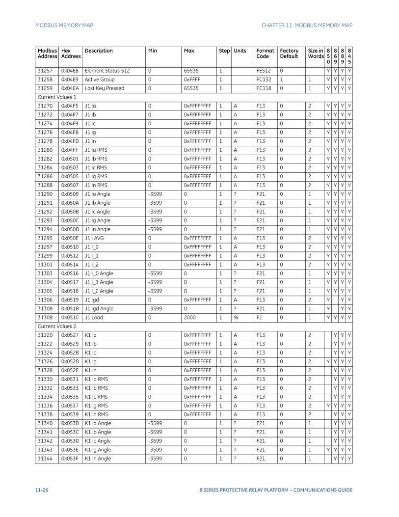
MODBUS MEMORY MAP CHAPTER 11: MODBUS MEMORY MAP
31257 0x04E8 Element Status 512 0 65535 1 FE512 0 Y Y Y Y
31258 0x04E9 Active Group 0 0xFFFF 1 FC132 1 1 Y Y Y Y
31259 0x04EA Last Key Pressed 0 65535 1 FC118 0 1 Y Y Y Y
Current Values 1
31270 0x04F5 J1 Ia 0 0xFFFFFFFF 1 A F13 0 2 Y Y Y Y
31272 0x04F7 J1 Ib 0 0xFFFFFFFF 1 A F13 0 2 Y Y Y Y
31274 0x04F9 J1 Ic 0 0xFFFFFFFF 1 A F13 0 2 Y Y Y Y
31276 0x04FB J1 Ig 0 0xFFFFFFFF 1 A F13 0 2 Y Y Y Y
31278 0x04FD J1 In 0 0xFFFFFFFF 1 A F13 0 2 Y Y Y Y
31280 0x04FF J1 Ia RMS 0 0xFFFFFFFF 1 A F13 0 2 Y Y Y Y
31282 0x0501 J1 Ib RMS 0 0xFFFFFFFF 1 A F13 0 2 Y Y Y Y
31284 0x0503 J1 Ic RMS 0 0xFFFFFFFF 1 A F13 0 2 Y Y Y Y
31286 0x0505 J1 Ig RMS 0 0xFFFFFFFF 1 A F13 0 2 Y Y Y Y
31288 0x0507 J1 In RMS 0 0xFFFFFFFF 1 A F13 0 2 Y Y Y Y
31290 0x0509 J1 Ia Angle -3599 0 1 ? F21 0 1 Y Y Y Y
31291 0x050A J1 Ib Angle -3599 0 1 ? F21 0 1 Y Y Y Y
31292 0x050B J1 Ic Angle -3599 0 1 ? F21 0 1 Y Y Y Y
31293 0x050C J1 Ig Angle -3599 0 1 ? F21 0 1 Y Y Y Y
31294 0x050D J1 In Angle -3599 0 1 ? F21 0 1 Y Y Y Y
31295 0x050E J1 I AVG 0 0xFFFFFFFF 1 A F13 0 2 Y Y Y Y
31297 0x0510 J1 I_0 0 0xFFFFFFFF 1 A F13 0 2 Y Y Y Y
31299 0x0512 J1 I_1 0 0xFFFFFFFF 1 A F13 0 2 Y Y Y Y
31301 0x0514 J1 I_2 0 0xFFFFFFFF 1 A F13 0 2 Y Y Y Y
31303 0x0516 J1 I_0 Angle -3599 0 1 ? F21 0 1 Y Y Y Y
31304 0x0517 J1 I_1 Angle -3599 0 1 ? F21 0 1 Y Y Y Y
31305 0x0518 J1 I_2 Angle -3599 0 1 ? F21 0 1 Y Y Y Y
31306 0x0519 J1 Igd 0 0xFFFFFFFF 1 A F13 0 2 Y Y Y
31308 0x051B J1 Igd Angle -3599 0 1 ? F21 0 1 Y Y Y
31309 0x051C J1 Load 0 2000 1 % F1 0 1 Y Y Y Y
Current Values 2
31320 0x0527 K1 Ia 0 0xFFFFFFFF 1 A F13 0 2 Y Y Y
31322 0x0529 K1 Ib 0 0xFFFFFFFF 1 A F13 0 2 Y Y Y
31324 0x052B K1 Ic 0 0xFFFFFFFF 1 A F13 0 2 Y Y Y
31326 0x052D K1 Ig 0 0xFFFFFFFF 1 A F13 0 2 Y Y Y Y
31328 0x052F K1 In 0 0xFFFFFFFF 1 A F13 0 2 Y Y Y
31330 0x0531 K1 Ia RMS 0 0xFFFFFFFF 1 A F13 0 2 Y Y Y
31332 0x0533 K1 Ib RMS 0 0xFFFFFFFF 1 A F13 0 2 Y Y Y
31334 0x0535 K1 Ic RMS 0 0xFFFFFFFF 1 A F13 0 2 Y Y Y
31336 0x0537 K1 Ig RMS 0 0xFFFFFFFF 1 A F13 0 2 Y Y Y Y
31338 0x0539 K1 In RMS 0 0xFFFFFFFF 1 A F13 0 2 Y Y Y
31340 0x053B K1 Ia Angle -3599 0 1 ? F21 0 1 Y Y Y
31341 0x053C K1 Ib Angle -3599 0 1 ? F21 0 1 Y Y Y
31342 0x053D K1 Ic Angle -3599 0 1 ? F21 0 1 Y Y Y
31343 0x053E K1 Ig Angle -3599 0 1 ? F21 0 1 Y Y Y Y
31344 0x053F K1 In Angle -3599 0 1 ? F21 0 1 Y Y Y
Modbus Address
Hex Address
Description Min Max Step Units Format Code
Factory Default
Size in Words
850
869
889
845
11-26 8 SERIES PROTECTIVE RELAY PLATFORM – COMMUNICATIONS GUIDE
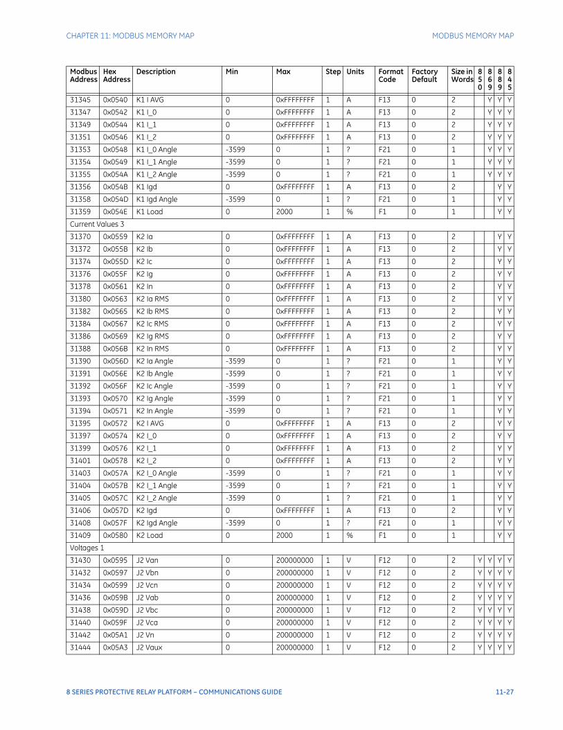
CHAPTER 11: MODBUS MEMORY MAP MODBUS MEMORY MAP
31345 0x0540 K1 I AVG 0 0xFFFFFFFF 1 A F13 0 2 Y Y Y
31347 0x0542 K1 I_0 0 0xFFFFFFFF 1 A F13 0 2 Y Y Y
31349 0x0544 K1 I_1 0 0xFFFFFFFF 1 A F13 0 2 Y Y Y
31351 0x0546 K1 I_2 0 0xFFFFFFFF 1 A F13 0 2 Y Y Y
31353 0x0548 K1 I_0 Angle -3599 0 1 ? F21 0 1 Y Y Y
31354 0x0549 K1 I_1 Angle -3599 0 1 ? F21 0 1 Y Y Y
31355 0x054A K1 I_2 Angle -3599 0 1 ? F21 0 1 Y Y Y
31356 0x054B K1 Igd 0 0xFFFFFFFF 1 A F13 0 2 Y Y
31358 0x054D K1 Igd Angle -3599 0 1 ? F21 0 1 Y Y
31359 0x054E K1 Load 0 2000 1 % F1 0 1 Y Y
Current Values 3
31370 0x0559 K2 Ia 0 0xFFFFFFFF 1 A F13 0 2 Y Y
31372 0x055B K2 Ib 0 0xFFFFFFFF 1 A F13 0 2 Y Y
31374 0x055D K2 Ic 0 0xFFFFFFFF 1 A F13 0 2 Y Y
31376 0x055F K2 Ig 0 0xFFFFFFFF 1 A F13 0 2 Y Y
31378 0x0561 K2 In 0 0xFFFFFFFF 1 A F13 0 2 Y Y
31380 0x0563 K2 Ia RMS 0 0xFFFFFFFF 1 A F13 0 2 Y Y
31382 0x0565 K2 Ib RMS 0 0xFFFFFFFF 1 A F13 0 2 Y Y
31384 0x0567 K2 Ic RMS 0 0xFFFFFFFF 1 A F13 0 2 Y Y
31386 0x0569 K2 Ig RMS 0 0xFFFFFFFF 1 A F13 0 2 Y Y
31388 0x056B K2 In RMS 0 0xFFFFFFFF 1 A F13 0 2 Y Y
31390 0x056D K2 Ia Angle -3599 0 1 ? F21 0 1 Y Y
31391 0x056E K2 Ib Angle -3599 0 1 ? F21 0 1 Y Y
31392 0x056F K2 Ic Angle -3599 0 1 ? F21 0 1 Y Y
31393 0x0570 K2 Ig Angle -3599 0 1 ? F21 0 1 Y Y
31394 0x0571 K2 In Angle -3599 0 1 ? F21 0 1 Y Y
31395 0x0572 K2 I AVG 0 0xFFFFFFFF 1 A F13 0 2 Y Y
31397 0x0574 K2 I_0 0 0xFFFFFFFF 1 A F13 0 2 Y Y
31399 0x0576 K2 I_1 0 0xFFFFFFFF 1 A F13 0 2 Y Y
31401 0x0578 K2 I_2 0 0xFFFFFFFF 1 A F13 0 2 Y Y
31403 0x057A K2 I_0 Angle -3599 0 1 ? F21 0 1 Y Y
31404 0x057B K2 I_1 Angle -3599 0 1 ? F21 0 1 Y Y
31405 0x057C K2 I_2 Angle -3599 0 1 ? F21 0 1 Y Y
31406 0x057D K2 Igd 0 0xFFFFFFFF 1 A F13 0 2 Y Y
31408 0x057F K2 Igd Angle -3599 0 1 ? F21 0 1 Y Y
31409 0x0580 K2 Load 0 2000 1 % F1 0 1 Y Y
Voltages 1
31430 0x0595 J2 Van 0 200000000 1 V F12 0 2 Y Y Y Y
31432 0x0597 J2 Vbn 0 200000000 1 V F12 0 2 Y Y Y Y
31434 0x0599 J2 Vcn 0 200000000 1 V F12 0 2 Y Y Y Y
31436 0x059B J2 Vab 0 200000000 1 V F12 0 2 Y Y Y Y
31438 0x059D J2 Vbc 0 200000000 1 V F12 0 2 Y Y Y Y
31440 0x059F J2 Vca 0 200000000 1 V F12 0 2 Y Y Y Y
31442 0x05A1 J2 Vn 0 200000000 1 V F12 0 2 Y Y Y Y
31444 0x05A3 J2 Vaux 0 200000000 1 V F12 0 2 Y Y Y Y
Modbus Address
Hex Address
Description Min Max Step Units Format Code
Factory Default
Size in Words
850
869
889
845
8 SERIES PROTECTIVE RELAY PLATFORM – COMMUNICATIONS GUIDE 11-27
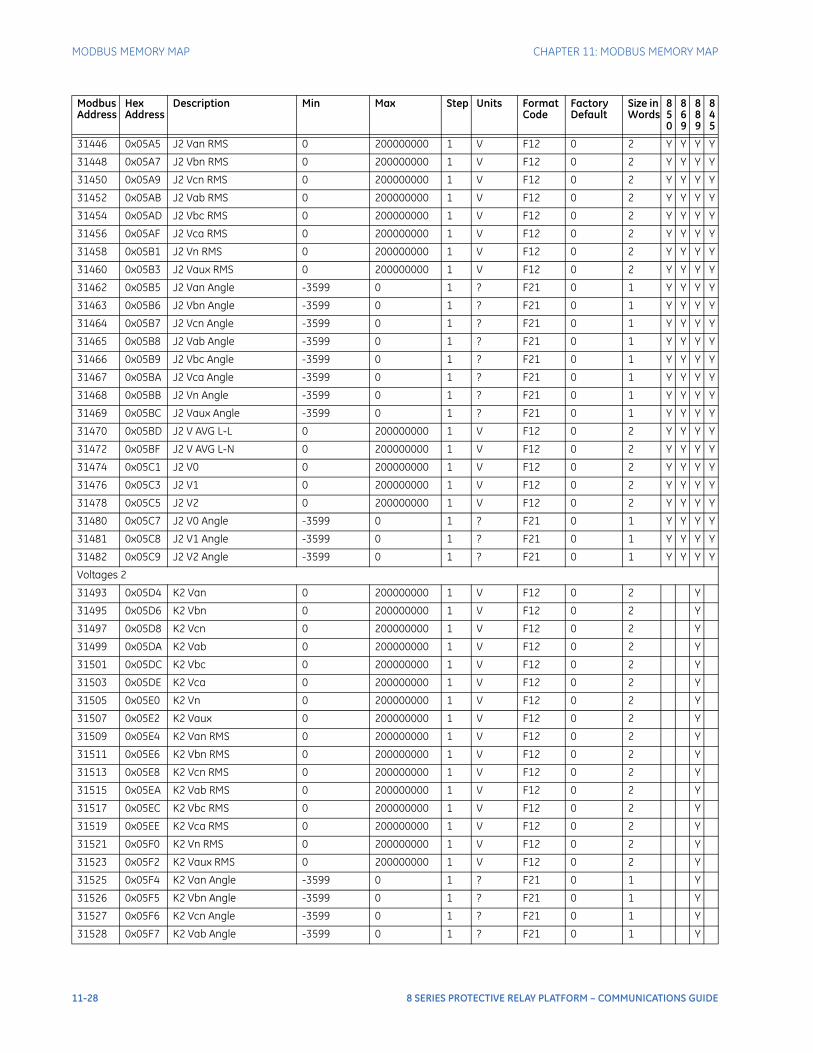
MODBUS MEMORY MAP CHAPTER 11: MODBUS MEMORY MAP
31446 0x05A5 J2 Van RMS 0 200000000 1 V F12 0 2 Y Y Y Y
31448 0x05A7 J2 Vbn RMS 0 200000000 1 V F12 0 2 Y Y Y Y
31450 0x05A9 J2 Vcn RMS 0 200000000 1 V F12 0 2 Y Y Y Y
31452 0x05AB J2 Vab RMS 0 200000000 1 V F12 0 2 Y Y Y Y
31454 0x05AD J2 Vbc RMS 0 200000000 1 V F12 0 2 Y Y Y Y
31456 0x05AF J2 Vca RMS 0 200000000 1 V F12 0 2 Y Y Y Y
31458 0x05B1 J2 Vn RMS 0 200000000 1 V F12 0 2 Y Y Y Y
31460 0x05B3 J2 Vaux RMS 0 200000000 1 V F12 0 2 Y Y Y Y
31462 0x05B5 J2 Van Angle -3599 0 1 ? F21 0 1 Y Y Y Y
31463 0x05B6 J2 Vbn Angle -3599 0 1 ? F21 0 1 Y Y Y Y
31464 0x05B7 J2 Vcn Angle -3599 0 1 ? F21 0 1 Y Y Y Y
31465 0x05B8 J2 Vab Angle -3599 0 1 ? F21 0 1 Y Y Y Y
31466 0x05B9 J2 Vbc Angle -3599 0 1 ? F21 0 1 Y Y Y Y
31467 0x05BA J2 Vca Angle -3599 0 1 ? F21 0 1 Y Y Y Y
31468 0x05BB J2 Vn Angle -3599 0 1 ? F21 0 1 Y Y Y Y
31469 0x05BC J2 Vaux Angle -3599 0 1 ? F21 0 1 Y Y Y Y
31470 0x05BD J2 V AVG L-L 0 200000000 1 V F12 0 2 Y Y Y Y
31472 0x05BF J2 V AVG L-N 0 200000000 1 V F12 0 2 Y Y Y Y
31474 0x05C1 J2 V0 0 200000000 1 V F12 0 2 Y Y Y Y
31476 0x05C3 J2 V1 0 200000000 1 V F12 0 2 Y Y Y Y
31478 0x05C5 J2 V2 0 200000000 1 V F12 0 2 Y Y Y Y
31480 0x05C7 J2 V0 Angle -3599 0 1 ? F21 0 1 Y Y Y Y
31481 0x05C8 J2 V1 Angle -3599 0 1 ? F21 0 1 Y Y Y Y
31482 0x05C9 J2 V2 Angle -3599 0 1 ? F21 0 1 Y Y Y Y
Voltages 2
31493 0x05D4 K2 Van 0 200000000 1 V F12 0 2 Y
31495 0x05D6 K2 Vbn 0 200000000 1 V F12 0 2 Y
31497 0x05D8 K2 Vcn 0 200000000 1 V F12 0 2 Y
31499 0x05DA K2 Vab 0 200000000 1 V F12 0 2 Y
31501 0x05DC K2 Vbc 0 200000000 1 V F12 0 2 Y
31503 0x05DE K2 Vca 0 200000000 1 V F12 0 2 Y
31505 0x05E0 K2 Vn 0 200000000 1 V F12 0 2 Y
31507 0x05E2 K2 Vaux 0 200000000 1 V F12 0 2 Y
31509 0x05E4 K2 Van RMS 0 200000000 1 V F12 0 2 Y
31511 0x05E6 K2 Vbn RMS 0 200000000 1 V F12 0 2 Y
31513 0x05E8 K2 Vcn RMS 0 200000000 1 V F12 0 2 Y
31515 0x05EA K2 Vab RMS 0 200000000 1 V F12 0 2 Y
31517 0x05EC K2 Vbc RMS 0 200000000 1 V F12 0 2 Y
31519 0x05EE K2 Vca RMS 0 200000000 1 V F12 0 2 Y
31521 0x05F0 K2 Vn RMS 0 200000000 1 V F12 0 2 Y
31523 0x05F2 K2 Vaux RMS 0 200000000 1 V F12 0 2 Y
31525 0x05F4 K2 Van Angle -3599 0 1 ? F21 0 1 Y
31526 0x05F5 K2 Vbn Angle -3599 0 1 ? F21 0 1 Y
31527 0x05F6 K2 Vcn Angle -3599 0 1 ? F21 0 1 Y
31528 0x05F7 K2 Vab Angle -3599 0 1 ? F21 0 1 Y
Modbus Address
Hex Address
Description Min Max Step Units Format Code
Factory Default
Size in Words
850
869
889
845
11-28 8 SERIES PROTECTIVE RELAY PLATFORM – COMMUNICATIONS GUIDE
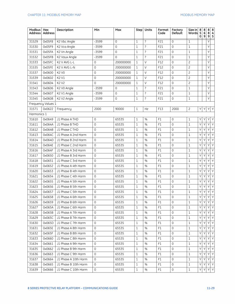
CHAPTER 11: MODBUS MEMORY MAP MODBUS MEMORY MAP
31529 0x05F8 K2 Vbc Angle -3599 0 1 ? F21 0 1 Y
31530 0x05F9 K2 Vca Angle -3599 0 1 ? F21 0 1 Y
31531 0x05FA K2 Vn Angle -3599 0 1 ? F21 0 1 Y
31532 0x05FB K2 Vaux Angle -3599 0 1 ? F21 0 1 Y
31533 0x05FC K2 V AVG L-L 0 200000000 1 V F12 0 2 Y
31535 0x05FE K2 V AVG L-N 0 200000000 1 V F12 0 2 Y
31537 0x0600 K2 V0 0 200000000 1 V F12 0 2 Y
31539 0x0602 K2 V1 0 200000000 1 V F12 0 2 Y
31541 0x0604 K2 V2 0 200000000 1 V F12 0 2 Y
31543 0x0606 K2 V0 Angle -3599 0 1 ? F21 0 1 Y
31544 0x0607 K2 V1 Angle -3599 0 1 ? F21 0 1 Y
31545 0x0608 K2 V2 Angle -3599 0 1 ? F21 0 1 Y
Frequency Values 1
31571 0x0622 Frequency 2000 90000 1 Hz F13 2000 2 Y Y Y Y
Harmonics 1
31610 0x0649 J1 Phase A THD 0 65535 1 % F1 0 1 Y Y Y Y
31611 0x064A J1 Phase B THD 0 65535 1 % F1 0 1 Y Y Y Y
31612 0x064B J1 Phase C THD 0 65535 1 % F1 0 1 Y Y Y Y
31613 0x064C J1 Phase A 2nd Harm 0 65535 1 % F1 0 1 Y Y Y Y
31614 0x064D J1 Phase B 2nd Harm 0 65535 1 % F1 0 1 Y Y Y Y
31615 0x064E J1 Phase C 2nd Harm 0 65535 1 % F1 0 1 Y Y Y Y
31616 0x064F J1 Phase A 3rd Harm 0 65535 1 % F1 0 1 Y Y Y Y
31617 0x0650 J1 Phase B 3rd Harm 0 65535 1 % F1 0 1 Y Y Y Y
31618 0x0651 J1 Phase C 3rd Harm 0 65535 1 % F1 0 1 Y Y Y Y
31619 0x0652 J1 Phase A 4th Harm 0 65535 1 % F1 0 1 Y Y Y Y
31620 0x0653 J1 Phase B 4th Harm 0 65535 1 % F1 0 1 Y Y Y Y
31621 0x0654 J1 Phase C 4th Harm 0 65535 1 % F1 0 1 Y Y Y Y
31622 0x0655 J1 Phase A 5th Harm 0 65535 1 % F1 0 1 Y Y Y Y
31623 0x0656 J1 Phase B 5th Harm 0 65535 1 % F1 0 1 Y Y Y Y
31624 0x0657 J1 Phase C 5th Harm 0 65535 1 % F1 0 1 Y Y Y Y
31625 0x0658 J1 Phase A 6th Harm 0 65535 1 % F1 0 1 Y Y Y Y
31626 0x0659 J1 Phase B 6th Harm 0 65535 1 % F1 0 1 Y Y Y Y
31627 0x065A J1 Phase C 6th Harm 0 65535 1 % F1 0 1 Y Y Y Y
31628 0x065B J1 Phase A 7th Harm 0 65535 1 % F1 0 1 Y Y Y Y
31629 0x065C J1 Phase B 7th Harm 0 65535 1 % F1 0 1 Y Y Y Y
31630 0x065D J1 Phase C 7th Harm 0 65535 1 % F1 0 1 Y Y Y Y
31631 0x065E J1 Phase A 8th Harm 0 65535 1 % F1 0 1 Y Y Y Y
31632 0x065F J1 Phase B 8th Harm 0 65535 1 % F1 0 1 Y Y Y Y
31633 0x0660 J1 Phase C 8th Harm 0 65535 1 % F1 0 1 Y Y Y Y
31634 0x0661 J1 Phase A 9th Harm 0 65535 1 % F1 0 1 Y Y Y Y
31635 0x0662 J1 Phase B 9th Harm 0 65535 1 % F1 0 1 Y Y Y Y
31636 0x0663 J1 Phase C 9th Harm 0 65535 1 % F1 0 1 Y Y Y Y
31637 0x0664 J1 Phase A 10th Harm 0 65535 1 % F1 0 1 Y Y Y Y
31638 0x0665 J1 Phase B 10th Harm 0 65535 1 % F1 0 1 Y Y Y Y
31639 0x0666 J1 Phase C 10th Harm 0 65535 1 % F1 0 1 Y Y Y Y
Modbus Address
Hex Address
Description Min Max Step Units Format Code
Factory Default
Size in Words
850
869
889
845
8 SERIES PROTECTIVE RELAY PLATFORM – COMMUNICATIONS GUIDE 11-29
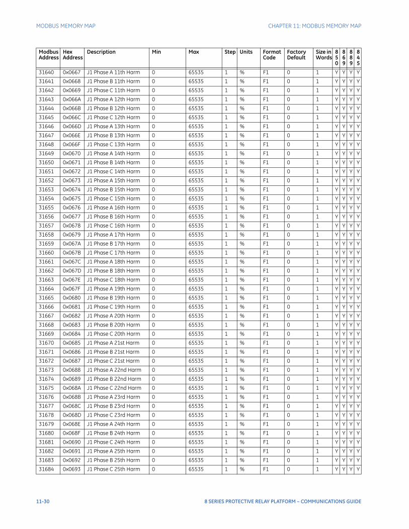
MODBUS MEMORY MAP CHAPTER 11: MODBUS MEMORY MAP
31640 0x0667 J1 Phase A 11th Harm 0 65535 1 % F1 0 1 Y Y Y Y
31641 0x0668 J1 Phase B 11th Harm 0 65535 1 % F1 0 1 Y Y Y Y
31642 0x0669 J1 Phase C 11th Harm 0 65535 1 % F1 0 1 Y Y Y Y
31643 0x066A J1 Phase A 12th Harm 0 65535 1 % F1 0 1 Y Y Y Y
31644 0x066B J1 Phase B 12th Harm 0 65535 1 % F1 0 1 Y Y Y Y
31645 0x066C J1 Phase C 12th Harm 0 65535 1 % F1 0 1 Y Y Y Y
31646 0x066D J1 Phase A 13th Harm 0 65535 1 % F1 0 1 Y Y Y Y
31647 0x066E J1 Phase B 13th Harm 0 65535 1 % F1 0 1 Y Y Y Y
31648 0x066F J1 Phase C 13th Harm 0 65535 1 % F1 0 1 Y Y Y Y
31649 0x0670 J1 Phase A 14th Harm 0 65535 1 % F1 0 1 Y Y Y Y
31650 0x0671 J1 Phase B 14th Harm 0 65535 1 % F1 0 1 Y Y Y Y
31651 0x0672 J1 Phase C 14th Harm 0 65535 1 % F1 0 1 Y Y Y Y
31652 0x0673 J1 Phase A 15th Harm 0 65535 1 % F1 0 1 Y Y Y Y
31653 0x0674 J1 Phase B 15th Harm 0 65535 1 % F1 0 1 Y Y Y Y
31654 0x0675 J1 Phase C 15th Harm 0 65535 1 % F1 0 1 Y Y Y Y
31655 0x0676 J1 Phase A 16th Harm 0 65535 1 % F1 0 1 Y Y Y Y
31656 0x0677 J1 Phase B 16th Harm 0 65535 1 % F1 0 1 Y Y Y Y
31657 0x0678 J1 Phase C 16th Harm 0 65535 1 % F1 0 1 Y Y Y Y
31658 0x0679 J1 Phase A 17th Harm 0 65535 1 % F1 0 1 Y Y Y Y
31659 0x067A J1 Phase B 17th Harm 0 65535 1 % F1 0 1 Y Y Y Y
31660 0x067B J1 Phase C 17th Harm 0 65535 1 % F1 0 1 Y Y Y Y
31661 0x067C J1 Phase A 18th Harm 0 65535 1 % F1 0 1 Y Y Y Y
31662 0x067D J1 Phase B 18th Harm 0 65535 1 % F1 0 1 Y Y Y Y
31663 0x067E J1 Phase C 18th Harm 0 65535 1 % F1 0 1 Y Y Y Y
31664 0x067F J1 Phase A 19th Harm 0 65535 1 % F1 0 1 Y Y Y Y
31665 0x0680 J1 Phase B 19th Harm 0 65535 1 % F1 0 1 Y Y Y Y
31666 0x0681 J1 Phase C 19th Harm 0 65535 1 % F1 0 1 Y Y Y Y
31667 0x0682 J1 Phase A 20th Harm 0 65535 1 % F1 0 1 Y Y Y Y
31668 0x0683 J1 Phase B 20th Harm 0 65535 1 % F1 0 1 Y Y Y Y
31669 0x0684 J1 Phase C 20th Harm 0 65535 1 % F1 0 1 Y Y Y Y
31670 0x0685 J1 Phase A 21st Harm 0 65535 1 % F1 0 1 Y Y Y Y
31671 0x0686 J1 Phase B 21st Harm 0 65535 1 % F1 0 1 Y Y Y Y
31672 0x0687 J1 Phase C 21st Harm 0 65535 1 % F1 0 1 Y Y Y Y
31673 0x0688 J1 Phase A 22nd Harm 0 65535 1 % F1 0 1 Y Y Y Y
31674 0x0689 J1 Phase B 22nd Harm 0 65535 1 % F1 0 1 Y Y Y Y
31675 0x068A J1 Phase C 22nd Harm 0 65535 1 % F1 0 1 Y Y Y Y
31676 0x068B J1 Phase A 23rd Harm 0 65535 1 % F1 0 1 Y Y Y Y
31677 0x068C J1 Phase B 23rd Harm 0 65535 1 % F1 0 1 Y Y Y Y
31678 0x068D J1 Phase C 23rd Harm 0 65535 1 % F1 0 1 Y Y Y Y
31679 0x068E J1 Phase A 24th Harm 0 65535 1 % F1 0 1 Y Y Y Y
31680 0x068F J1 Phase B 24th Harm 0 65535 1 % F1 0 1 Y Y Y Y
31681 0x0690 J1 Phase C 24th Harm 0 65535 1 % F1 0 1 Y Y Y Y
31682 0x0691 J1 Phase A 25th Harm 0 65535 1 % F1 0 1 Y Y Y Y
31683 0x0692 J1 Phase B 25th Harm 0 65535 1 % F1 0 1 Y Y Y Y
31684 0x0693 J1 Phase C 25th Harm 0 65535 1 % F1 0 1 Y Y Y Y
Modbus Address
Hex Address
Description Min Max Step Units Format Code
Factory Default
Size in Words
850
869
889
845
11-30 8 SERIES PROTECTIVE RELAY PLATFORM – COMMUNICATIONS GUIDE
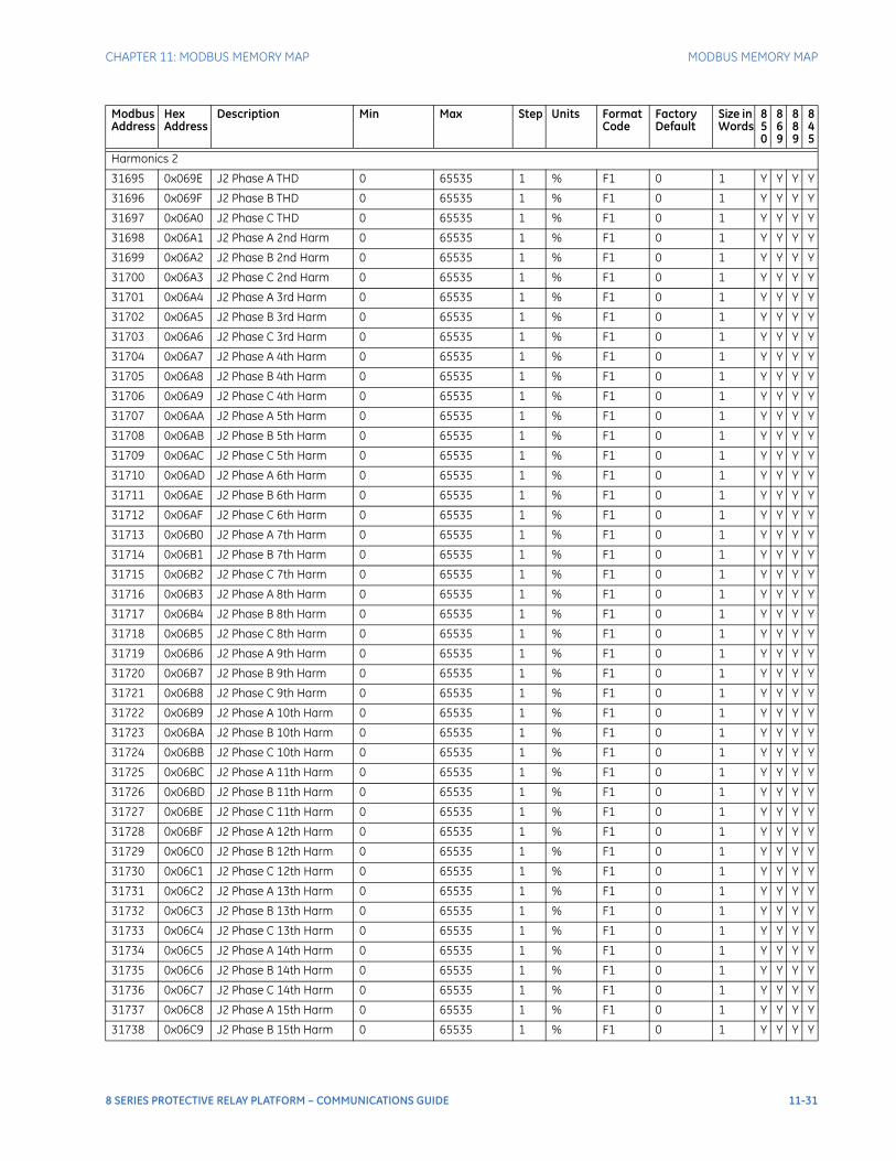
CHAPTER 11: MODBUS MEMORY MAP MODBUS MEMORY MAP
Harmonics 2
31695 0x069E J2 Phase A THD 0 65535 1 % F1 0 1 Y Y Y Y
31696 0x069F J2 Phase B THD 0 65535 1 % F1 0 1 Y Y Y Y
31697 0x06A0 J2 Phase C THD 0 65535 1 % F1 0 1 Y Y Y Y
31698 0x06A1 J2 Phase A 2nd Harm 0 65535 1 % F1 0 1 Y Y Y Y
31699 0x06A2 J2 Phase B 2nd Harm 0 65535 1 % F1 0 1 Y Y Y Y
31700 0x06A3 J2 Phase C 2nd Harm 0 65535 1 % F1 0 1 Y Y Y Y
31701 0x06A4 J2 Phase A 3rd Harm 0 65535 1 % F1 0 1 Y Y Y Y
31702 0x06A5 J2 Phase B 3rd Harm 0 65535 1 % F1 0 1 Y Y Y Y
31703 0x06A6 J2 Phase C 3rd Harm 0 65535 1 % F1 0 1 Y Y Y Y
31704 0x06A7 J2 Phase A 4th Harm 0 65535 1 % F1 0 1 Y Y Y Y
31705 0x06A8 J2 Phase B 4th Harm 0 65535 1 % F1 0 1 Y Y Y Y
31706 0x06A9 J2 Phase C 4th Harm 0 65535 1 % F1 0 1 Y Y Y Y
31707 0x06AA J2 Phase A 5th Harm 0 65535 1 % F1 0 1 Y Y Y Y
31708 0x06AB J2 Phase B 5th Harm 0 65535 1 % F1 0 1 Y Y Y Y
31709 0x06AC J2 Phase C 5th Harm 0 65535 1 % F1 0 1 Y Y Y Y
31710 0x06AD J2 Phase A 6th Harm 0 65535 1 % F1 0 1 Y Y Y Y
31711 0x06AE J2 Phase B 6th Harm 0 65535 1 % F1 0 1 Y Y Y Y
31712 0x06AF J2 Phase C 6th Harm 0 65535 1 % F1 0 1 Y Y Y Y
31713 0x06B0 J2 Phase A 7th Harm 0 65535 1 % F1 0 1 Y Y Y Y
31714 0x06B1 J2 Phase B 7th Harm 0 65535 1 % F1 0 1 Y Y Y Y
31715 0x06B2 J2 Phase C 7th Harm 0 65535 1 % F1 0 1 Y Y Y Y
31716 0x06B3 J2 Phase A 8th Harm 0 65535 1 % F1 0 1 Y Y Y Y
31717 0x06B4 J2 Phase B 8th Harm 0 65535 1 % F1 0 1 Y Y Y Y
31718 0x06B5 J2 Phase C 8th Harm 0 65535 1 % F1 0 1 Y Y Y Y
31719 0x06B6 J2 Phase A 9th Harm 0 65535 1 % F1 0 1 Y Y Y Y
31720 0x06B7 J2 Phase B 9th Harm 0 65535 1 % F1 0 1 Y Y Y Y
31721 0x06B8 J2 Phase C 9th Harm 0 65535 1 % F1 0 1 Y Y Y Y
31722 0x06B9 J2 Phase A 10th Harm 0 65535 1 % F1 0 1 Y Y Y Y
31723 0x06BA J2 Phase B 10th Harm 0 65535 1 % F1 0 1 Y Y Y Y
31724 0x06BB J2 Phase C 10th Harm 0 65535 1 % F1 0 1 Y Y Y Y
31725 0x06BC J2 Phase A 11th Harm 0 65535 1 % F1 0 1 Y Y Y Y
31726 0x06BD J2 Phase B 11th Harm 0 65535 1 % F1 0 1 Y Y Y Y
31727 0x06BE J2 Phase C 11th Harm 0 65535 1 % F1 0 1 Y Y Y Y
31728 0x06BF J2 Phase A 12th Harm 0 65535 1 % F1 0 1 Y Y Y Y
31729 0x06C0 J2 Phase B 12th Harm 0 65535 1 % F1 0 1 Y Y Y Y
31730 0x06C1 J2 Phase C 12th Harm 0 65535 1 % F1 0 1 Y Y Y Y
31731 0x06C2 J2 Phase A 13th Harm 0 65535 1 % F1 0 1 Y Y Y Y
31732 0x06C3 J2 Phase B 13th Harm 0 65535 1 % F1 0 1 Y Y Y Y
31733 0x06C4 J2 Phase C 13th Harm 0 65535 1 % F1 0 1 Y Y Y Y
31734 0x06C5 J2 Phase A 14th Harm 0 65535 1 % F1 0 1 Y Y Y Y
31735 0x06C6 J2 Phase B 14th Harm 0 65535 1 % F1 0 1 Y Y Y Y
31736 0x06C7 J2 Phase C 14th Harm 0 65535 1 % F1 0 1 Y Y Y Y
31737 0x06C8 J2 Phase A 15th Harm 0 65535 1 % F1 0 1 Y Y Y Y
31738 0x06C9 J2 Phase B 15th Harm 0 65535 1 % F1 0 1 Y Y Y Y
Modbus Address
Hex Address
Description Min Max Step Units Format Code
Factory Default
Size in Words
850
869
889
845
8 SERIES PROTECTIVE RELAY PLATFORM – COMMUNICATIONS GUIDE 11-31
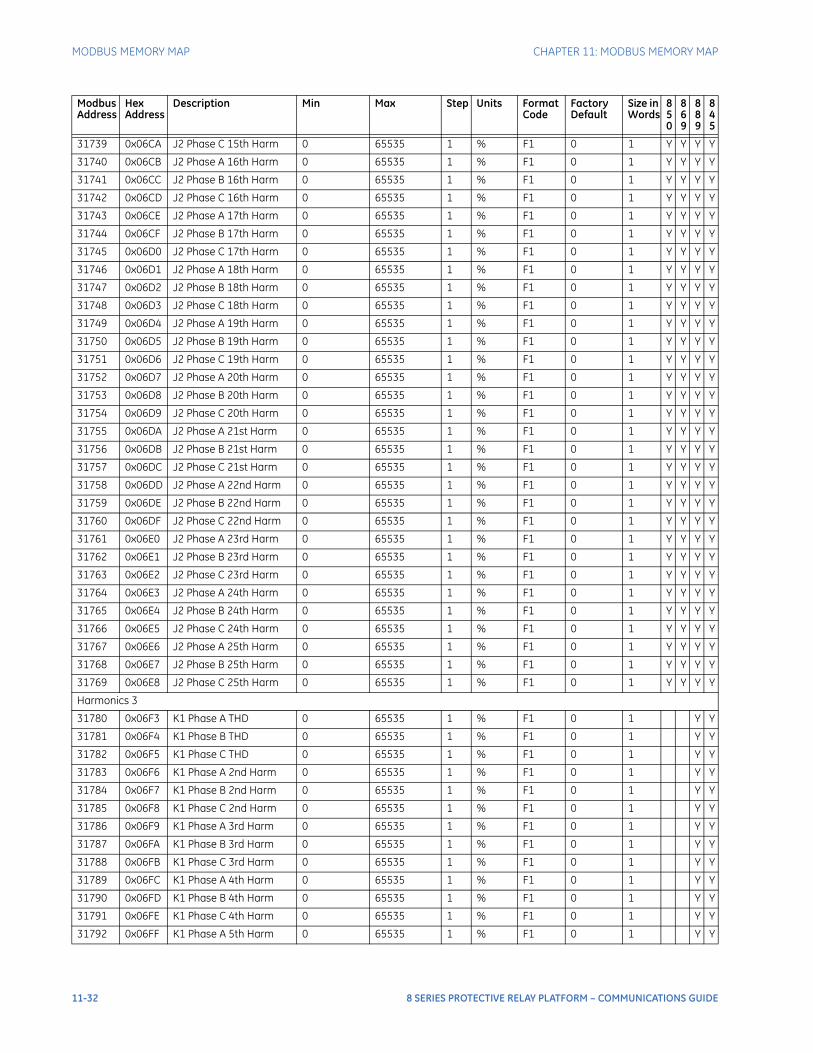
MODBUS MEMORY MAP CHAPTER 11: MODBUS MEMORY MAP
31739 0x06CA J2 Phase C 15th Harm 0 65535 1 % F1 0 1 Y Y Y Y
31740 0x06CB J2 Phase A 16th Harm 0 65535 1 % F1 0 1 Y Y Y Y
31741 0x06CC J2 Phase B 16th Harm 0 65535 1 % F1 0 1 Y Y Y Y
31742 0x06CD J2 Phase C 16th Harm 0 65535 1 % F1 0 1 Y Y Y Y
31743 0x06CE J2 Phase A 17th Harm 0 65535 1 % F1 0 1 Y Y Y Y
31744 0x06CF J2 Phase B 17th Harm 0 65535 1 % F1 0 1 Y Y Y Y
31745 0x06D0 J2 Phase C 17th Harm 0 65535 1 % F1 0 1 Y Y Y Y
31746 0x06D1 J2 Phase A 18th Harm 0 65535 1 % F1 0 1 Y Y Y Y
31747 0x06D2 J2 Phase B 18th Harm 0 65535 1 % F1 0 1 Y Y Y Y
31748 0x06D3 J2 Phase C 18th Harm 0 65535 1 % F1 0 1 Y Y Y Y
31749 0x06D4 J2 Phase A 19th Harm 0 65535 1 % F1 0 1 Y Y Y Y
31750 0x06D5 J2 Phase B 19th Harm 0 65535 1 % F1 0 1 Y Y Y Y
31751 0x06D6 J2 Phase C 19th Harm 0 65535 1 % F1 0 1 Y Y Y Y
31752 0x06D7 J2 Phase A 20th Harm 0 65535 1 % F1 0 1 Y Y Y Y
31753 0x06D8 J2 Phase B 20th Harm 0 65535 1 % F1 0 1 Y Y Y Y
31754 0x06D9 J2 Phase C 20th Harm 0 65535 1 % F1 0 1 Y Y Y Y
31755 0x06DA J2 Phase A 21st Harm 0 65535 1 % F1 0 1 Y Y Y Y
31756 0x06DB J2 Phase B 21st Harm 0 65535 1 % F1 0 1 Y Y Y Y
31757 0x06DC J2 Phase C 21st Harm 0 65535 1 % F1 0 1 Y Y Y Y
31758 0x06DD J2 Phase A 22nd Harm 0 65535 1 % F1 0 1 Y Y Y Y
31759 0x06DE J2 Phase B 22nd Harm 0 65535 1 % F1 0 1 Y Y Y Y
31760 0x06DF J2 Phase C 22nd Harm 0 65535 1 % F1 0 1 Y Y Y Y
31761 0x06E0 J2 Phase A 23rd Harm 0 65535 1 % F1 0 1 Y Y Y Y
31762 0x06E1 J2 Phase B 23rd Harm 0 65535 1 % F1 0 1 Y Y Y Y
31763 0x06E2 J2 Phase C 23rd Harm 0 65535 1 % F1 0 1 Y Y Y Y
31764 0x06E3 J2 Phase A 24th Harm 0 65535 1 % F1 0 1 Y Y Y Y
31765 0x06E4 J2 Phase B 24th Harm 0 65535 1 % F1 0 1 Y Y Y Y
31766 0x06E5 J2 Phase C 24th Harm 0 65535 1 % F1 0 1 Y Y Y Y
31767 0x06E6 J2 Phase A 25th Harm 0 65535 1 % F1 0 1 Y Y Y Y
31768 0x06E7 J2 Phase B 25th Harm 0 65535 1 % F1 0 1 Y Y Y Y
31769 0x06E8 J2 Phase C 25th Harm 0 65535 1 % F1 0 1 Y Y Y Y
Harmonics 3
31780 0x06F3 K1 Phase A THD 0 65535 1 % F1 0 1 Y Y
31781 0x06F4 K1 Phase B THD 0 65535 1 % F1 0 1 Y Y
31782 0x06F5 K1 Phase C THD 0 65535 1 % F1 0 1 Y Y
31783 0x06F6 K1 Phase A 2nd Harm 0 65535 1 % F1 0 1 Y Y
31784 0x06F7 K1 Phase B 2nd Harm 0 65535 1 % F1 0 1 Y Y
31785 0x06F8 K1 Phase C 2nd Harm 0 65535 1 % F1 0 1 Y Y
31786 0x06F9 K1 Phase A 3rd Harm 0 65535 1 % F1 0 1 Y Y
31787 0x06FA K1 Phase B 3rd Harm 0 65535 1 % F1 0 1 Y Y
31788 0x06FB K1 Phase C 3rd Harm 0 65535 1 % F1 0 1 Y Y
31789 0x06FC K1 Phase A 4th Harm 0 65535 1 % F1 0 1 Y Y
31790 0x06FD K1 Phase B 4th Harm 0 65535 1 % F1 0 1 Y Y
31791 0x06FE K1 Phase C 4th Harm 0 65535 1 % F1 0 1 Y Y
31792 0x06FF K1 Phase A 5th Harm 0 65535 1 % F1 0 1 Y Y
Modbus Address
Hex Address
Description Min Max Step Units Format Code
Factory Default
Size in Words
850
869
889
845
11-32 8 SERIES PROTECTIVE RELAY PLATFORM – COMMUNICATIONS GUIDE
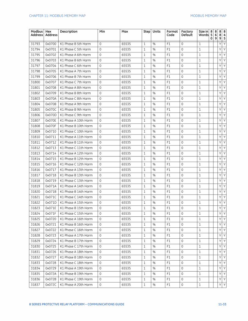
CHAPTER 11: MODBUS MEMORY MAP MODBUS MEMORY MAP
31793 0x0700 K1 Phase B 5th Harm 0 65535 1 % F1 0 1 Y Y
31794 0x0701 K1 Phase C 5th Harm 0 65535 1 % F1 0 1 Y Y
31795 0x0702 K1 Phase A 6th Harm 0 65535 1 % F1 0 1 Y Y
31796 0x0703 K1 Phase B 6th Harm 0 65535 1 % F1 0 1 Y Y
31797 0x0704 K1 Phase C 6th Harm 0 65535 1 % F1 0 1 Y Y
31798 0x0705 K1 Phase A 7th Harm 0 65535 1 % F1 0 1 Y Y
31799 0x0706 K1 Phase B 7th Harm 0 65535 1 % F1 0 1 Y Y
31800 0x0707 K1 Phase C 7th Harm 0 65535 1 % F1 0 1 Y Y
31801 0x0708 K1 Phase A 8th Harm 0 65535 1 % F1 0 1 Y Y
31802 0x0709 K1 Phase B 8th Harm 0 65535 1 % F1 0 1 Y Y
31803 0x070A K1 Phase C 8th Harm 0 65535 1 % F1 0 1 Y Y
31804 0x070B K1 Phase A 9th Harm 0 65535 1 % F1 0 1 Y Y
31805 0x070C K1 Phase B 9th Harm 0 65535 1 % F1 0 1 Y Y
31806 0x070D K1 Phase C 9th Harm 0 65535 1 % F1 0 1 Y Y
31807 0x070E K1 Phase A 10th Harm 0 65535 1 % F1 0 1 Y Y
31808 0x070F K1 Phase B 10th Harm 0 65535 1 % F1 0 1 Y Y
31809 0x0710 K1 Phase C 10th Harm 0 65535 1 % F1 0 1 Y Y
31810 0x0711 K1 Phase A 11th Harm 0 65535 1 % F1 0 1 Y Y
31811 0x0712 K1 Phase B 11th Harm 0 65535 1 % F1 0 1 Y Y
31812 0x0713 K1 Phase C 11th Harm 0 65535 1 % F1 0 1 Y Y
31813 0x0714 K1 Phase A 12th Harm 0 65535 1 % F1 0 1 Y Y
31814 0x0715 K1 Phase B 12th Harm 0 65535 1 % F1 0 1 Y Y
31815 0x0716 K1 Phase C 12th Harm 0 65535 1 % F1 0 1 Y Y
31816 0x0717 K1 Phase A 13th Harm 0 65535 1 % F1 0 1 Y Y
31817 0x0718 K1 Phase B 13th Harm 0 65535 1 % F1 0 1 Y Y
31818 0x0719 K1 Phase C 13th Harm 0 65535 1 % F1 0 1 Y Y
31819 0x071A K1 Phase A 14th Harm 0 65535 1 % F1 0 1 Y Y
31820 0x071B K1 Phase B 14th Harm 0 65535 1 % F1 0 1 Y Y
31821 0x071C K1 Phase C 14th Harm 0 65535 1 % F1 0 1 Y Y
31822 0x071D K1 Phase A 15th Harm 0 65535 1 % F1 0 1 Y Y
31823 0x071E K1 Phase B 15th Harm 0 65535 1 % F1 0 1 Y Y
31824 0x071F K1 Phase C 15th Harm 0 65535 1 % F1 0 1 Y Y
31825 0x0720 K1 Phase A 16th Harm 0 65535 1 % F1 0 1 Y Y
31826 0x0721 K1 Phase B 16th Harm 0 65535 1 % F1 0 1 Y Y
31827 0x0722 K1 Phase C 16th Harm 0 65535 1 % F1 0 1 Y Y
31828 0x0723 K1 Phase A 17th Harm 0 65535 1 % F1 0 1 Y Y
31829 0x0724 K1 Phase B 17th Harm 0 65535 1 % F1 0 1 Y Y
31830 0x0725 K1 Phase C 17th Harm 0 65535 1 % F1 0 1 Y Y
31831 0x0726 K1 Phase A 18th Harm 0 65535 1 % F1 0 1 Y Y
31832 0x0727 K1 Phase B 18th Harm 0 65535 1 % F1 0 1 Y Y
31833 0x0728 K1 Phase C 18th Harm 0 65535 1 % F1 0 1 Y Y
31834 0x0729 K1 Phase A 19th Harm 0 65535 1 % F1 0 1 Y Y
31835 0x072A K1 Phase B 19th Harm 0 65535 1 % F1 0 1 Y Y
31836 0x072B K1 Phase C 19th Harm 0 65535 1 % F1 0 1 Y Y
31837 0x072C K1 Phase A 20th Harm 0 65535 1 % F1 0 1 Y Y
Modbus Address
Hex Address
Description Min Max Step Units Format Code
Factory Default
Size in Words
850
869
889
845
8 SERIES PROTECTIVE RELAY PLATFORM – COMMUNICATIONS GUIDE 11-33
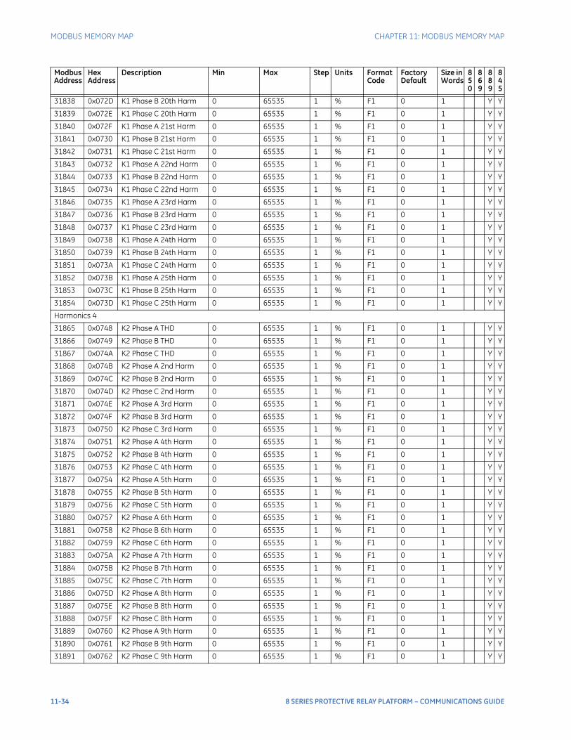
MODBUS MEMORY MAP CHAPTER 11: MODBUS MEMORY MAP
31838 0x072D K1 Phase B 20th Harm 0 65535 1 % F1 0 1 Y Y
31839 0x072E K1 Phase C 20th Harm 0 65535 1 % F1 0 1 Y Y
31840 0x072F K1 Phase A 21st Harm 0 65535 1 % F1 0 1 Y Y
31841 0x0730 K1 Phase B 21st Harm 0 65535 1 % F1 0 1 Y Y
31842 0x0731 K1 Phase C 21st Harm 0 65535 1 % F1 0 1 Y Y
31843 0x0732 K1 Phase A 22nd Harm 0 65535 1 % F1 0 1 Y Y
31844 0x0733 K1 Phase B 22nd Harm 0 65535 1 % F1 0 1 Y Y
31845 0x0734 K1 Phase C 22nd Harm 0 65535 1 % F1 0 1 Y Y
31846 0x0735 K1 Phase A 23rd Harm 0 65535 1 % F1 0 1 Y Y
31847 0x0736 K1 Phase B 23rd Harm 0 65535 1 % F1 0 1 Y Y
31848 0x0737 K1 Phase C 23rd Harm 0 65535 1 % F1 0 1 Y Y
31849 0x0738 K1 Phase A 24th Harm 0 65535 1 % F1 0 1 Y Y
31850 0x0739 K1 Phase B 24th Harm 0 65535 1 % F1 0 1 Y Y
31851 0x073A K1 Phase C 24th Harm 0 65535 1 % F1 0 1 Y Y
31852 0x073B K1 Phase A 25th Harm 0 65535 1 % F1 0 1 Y Y
31853 0x073C K1 Phase B 25th Harm 0 65535 1 % F1 0 1 Y Y
31854 0x073D K1 Phase C 25th Harm 0 65535 1 % F1 0 1 Y Y
Harmonics 4
31865 0x0748 K2 Phase A THD 0 65535 1 % F1 0 1 Y Y
31866 0x0749 K2 Phase B THD 0 65535 1 % F1 0 1 Y Y
31867 0x074A K2 Phase C THD 0 65535 1 % F1 0 1 Y Y
31868 0x074B K2 Phase A 2nd Harm 0 65535 1 % F1 0 1 Y Y
31869 0x074C K2 Phase B 2nd Harm 0 65535 1 % F1 0 1 Y Y
31870 0x074D K2 Phase C 2nd Harm 0 65535 1 % F1 0 1 Y Y
31871 0x074E K2 Phase A 3rd Harm 0 65535 1 % F1 0 1 Y Y
31872 0x074F K2 Phase B 3rd Harm 0 65535 1 % F1 0 1 Y Y
31873 0x0750 K2 Phase C 3rd Harm 0 65535 1 % F1 0 1 Y Y
31874 0x0751 K2 Phase A 4th Harm 0 65535 1 % F1 0 1 Y Y
31875 0x0752 K2 Phase B 4th Harm 0 65535 1 % F1 0 1 Y Y
31876 0x0753 K2 Phase C 4th Harm 0 65535 1 % F1 0 1 Y Y
31877 0x0754 K2 Phase A 5th Harm 0 65535 1 % F1 0 1 Y Y
31878 0x0755 K2 Phase B 5th Harm 0 65535 1 % F1 0 1 Y Y
31879 0x0756 K2 Phase C 5th Harm 0 65535 1 % F1 0 1 Y Y
31880 0x0757 K2 Phase A 6th Harm 0 65535 1 % F1 0 1 Y Y
31881 0x0758 K2 Phase B 6th Harm 0 65535 1 % F1 0 1 Y Y
31882 0x0759 K2 Phase C 6th Harm 0 65535 1 % F1 0 1 Y Y
31883 0x075A K2 Phase A 7th Harm 0 65535 1 % F1 0 1 Y Y
31884 0x075B K2 Phase B 7th Harm 0 65535 1 % F1 0 1 Y Y
31885 0x075C K2 Phase C 7th Harm 0 65535 1 % F1 0 1 Y Y
31886 0x075D K2 Phase A 8th Harm 0 65535 1 % F1 0 1 Y Y
31887 0x075E K2 Phase B 8th Harm 0 65535 1 % F1 0 1 Y Y
31888 0x075F K2 Phase C 8th Harm 0 65535 1 % F1 0 1 Y Y
31889 0x0760 K2 Phase A 9th Harm 0 65535 1 % F1 0 1 Y Y
31890 0x0761 K2 Phase B 9th Harm 0 65535 1 % F1 0 1 Y Y
31891 0x0762 K2 Phase C 9th Harm 0 65535 1 % F1 0 1 Y Y
Modbus Address
Hex Address
Description Min Max Step Units Format Code
Factory Default
Size in Words
850
869
889
845
11-34 8 SERIES PROTECTIVE RELAY PLATFORM – COMMUNICATIONS GUIDE
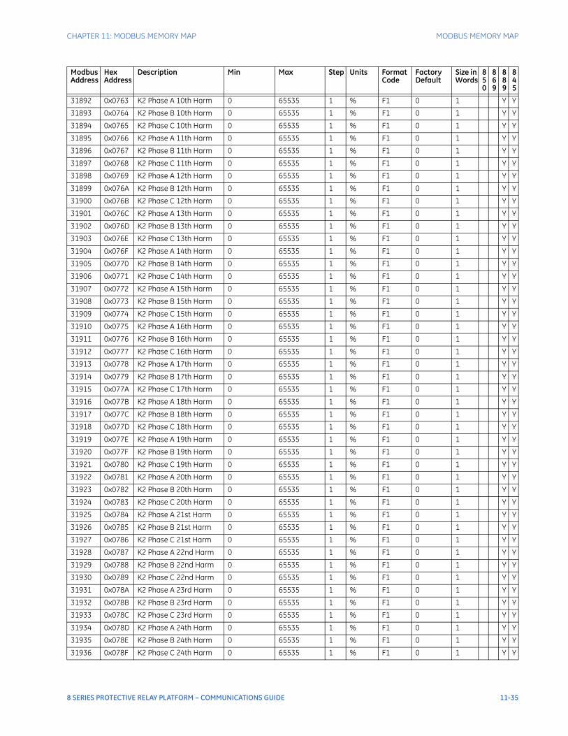
CHAPTER 11: MODBUS MEMORY MAP MODBUS MEMORY MAP
31892 0x0763 K2 Phase A 10th Harm 0 65535 1 % F1 0 1 Y Y
31893 0x0764 K2 Phase B 10th Harm 0 65535 1 % F1 0 1 Y Y
31894 0x0765 K2 Phase C 10th Harm 0 65535 1 % F1 0 1 Y Y
31895 0x0766 K2 Phase A 11th Harm 0 65535 1 % F1 0 1 Y Y
31896 0x0767 K2 Phase B 11th Harm 0 65535 1 % F1 0 1 Y Y
31897 0x0768 K2 Phase C 11th Harm 0 65535 1 % F1 0 1 Y Y
31898 0x0769 K2 Phase A 12th Harm 0 65535 1 % F1 0 1 Y Y
31899 0x076A K2 Phase B 12th Harm 0 65535 1 % F1 0 1 Y Y
31900 0x076B K2 Phase C 12th Harm 0 65535 1 % F1 0 1 Y Y
31901 0x076C K2 Phase A 13th Harm 0 65535 1 % F1 0 1 Y Y
31902 0x076D K2 Phase B 13th Harm 0 65535 1 % F1 0 1 Y Y
31903 0x076E K2 Phase C 13th Harm 0 65535 1 % F1 0 1 Y Y
31904 0x076F K2 Phase A 14th Harm 0 65535 1 % F1 0 1 Y Y
31905 0x0770 K2 Phase B 14th Harm 0 65535 1 % F1 0 1 Y Y
31906 0x0771 K2 Phase C 14th Harm 0 65535 1 % F1 0 1 Y Y
31907 0x0772 K2 Phase A 15th Harm 0 65535 1 % F1 0 1 Y Y
31908 0x0773 K2 Phase B 15th Harm 0 65535 1 % F1 0 1 Y Y
31909 0x0774 K2 Phase C 15th Harm 0 65535 1 % F1 0 1 Y Y
31910 0x0775 K2 Phase A 16th Harm 0 65535 1 % F1 0 1 Y Y
31911 0x0776 K2 Phase B 16th Harm 0 65535 1 % F1 0 1 Y Y
31912 0x0777 K2 Phase C 16th Harm 0 65535 1 % F1 0 1 Y Y
31913 0x0778 K2 Phase A 17th Harm 0 65535 1 % F1 0 1 Y Y
31914 0x0779 K2 Phase B 17th Harm 0 65535 1 % F1 0 1 Y Y
31915 0x077A K2 Phase C 17th Harm 0 65535 1 % F1 0 1 Y Y
31916 0x077B K2 Phase A 18th Harm 0 65535 1 % F1 0 1 Y Y
31917 0x077C K2 Phase B 18th Harm 0 65535 1 % F1 0 1 Y Y
31918 0x077D K2 Phase C 18th Harm 0 65535 1 % F1 0 1 Y Y
31919 0x077E K2 Phase A 19th Harm 0 65535 1 % F1 0 1 Y Y
31920 0x077F K2 Phase B 19th Harm 0 65535 1 % F1 0 1 Y Y
31921 0x0780 K2 Phase C 19th Harm 0 65535 1 % F1 0 1 Y Y
31922 0x0781 K2 Phase A 20th Harm 0 65535 1 % F1 0 1 Y Y
31923 0x0782 K2 Phase B 20th Harm 0 65535 1 % F1 0 1 Y Y
31924 0x0783 K2 Phase C 20th Harm 0 65535 1 % F1 0 1 Y Y
31925 0x0784 K2 Phase A 21st Harm 0 65535 1 % F1 0 1 Y Y
31926 0x0785 K2 Phase B 21st Harm 0 65535 1 % F1 0 1 Y Y
31927 0x0786 K2 Phase C 21st Harm 0 65535 1 % F1 0 1 Y Y
31928 0x0787 K2 Phase A 22nd Harm 0 65535 1 % F1 0 1 Y Y
31929 0x0788 K2 Phase B 22nd Harm 0 65535 1 % F1 0 1 Y Y
31930 0x0789 K2 Phase C 22nd Harm 0 65535 1 % F1 0 1 Y Y
31931 0x078A K2 Phase A 23rd Harm 0 65535 1 % F1 0 1 Y Y
31932 0x078B K2 Phase B 23rd Harm 0 65535 1 % F1 0 1 Y Y
31933 0x078C K2 Phase C 23rd Harm 0 65535 1 % F1 0 1 Y Y
31934 0x078D K2 Phase A 24th Harm 0 65535 1 % F1 0 1 Y Y
31935 0x078E K2 Phase B 24th Harm 0 65535 1 % F1 0 1 Y Y
31936 0x078F K2 Phase C 24th Harm 0 65535 1 % F1 0 1 Y Y
Modbus Address
Hex Address
Description Min Max Step Units Format Code
Factory Default
Size in Words
850
869
889
845
8 SERIES PROTECTIVE RELAY PLATFORM – COMMUNICATIONS GUIDE 11-35
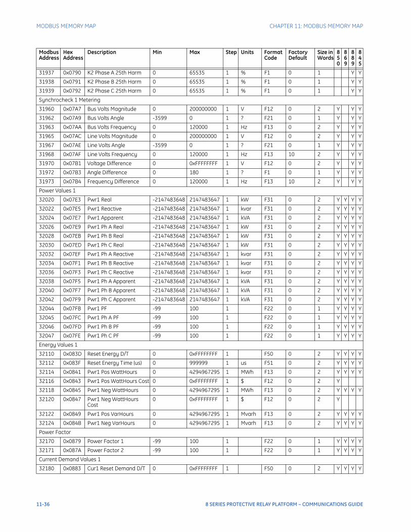
MODBUS MEMORY MAP CHAPTER 11: MODBUS MEMORY MAP
31937 0x0790 K2 Phase A 25th Harm 0 65535 1 % F1 0 1 Y Y
31938 0x0791 K2 Phase B 25th Harm 0 65535 1 % F1 0 1 Y Y
31939 0x0792 K2 Phase C 25th Harm 0 65535 1 % F1 0 1 Y Y
Synchrocheck 1 Metering
31960 0x07A7 Bus Volts Magnitude 0 200000000 1 V F12 0 2 Y Y Y
31962 0x07A9 Bus Volts Angle -3599 0 1 ? F21 0 1 Y Y Y
31963 0x07AA Bus Volts Frequency 0 120000 1 Hz F13 0 2 Y Y Y
31965 0x07AC Line Volts Magnitude 0 200000000 1 V F12 0 2 Y Y Y
31967 0x07AE Line Volts Angle -3599 0 1 ? F21 0 1 Y Y Y
31968 0x07AF Line Volts Frequency 0 120000 1 Hz F13 10 2 Y Y Y
31970 0x07B1 Voltage Difference 0 0xFFFFFFFF 1 V F12 0 2 Y Y Y
31972 0x07B3 Angle Difference 0 180 1 ? F1 0 1 Y Y Y
31973 0x07B4 Frequency Difference 0 120000 1 Hz F13 10 2 Y Y Y
Power Values 1
32020 0x07E3 Pwr1 Real -2147483648 2147483647 1 kW F31 0 2 Y Y Y Y
32022 0x07E5 Pwr1 Reactive -2147483648 2147483647 1 kvar F31 0 2 Y Y Y Y
32024 0x07E7 Pwr1 Apparent -2147483648 2147483647 1 kVA F31 0 2 Y Y Y Y
32026 0x07E9 Pwr1 Ph A Real -2147483648 2147483647 1 kW F31 0 2 Y Y Y Y
32028 0x07EB Pwr1 Ph B Real -2147483648 2147483647 1 kW F31 0 2 Y Y Y Y
32030 0x07ED Pwr1 Ph C Real -2147483648 2147483647 1 kW F31 0 2 Y Y Y Y
32032 0x07EF Pwr1 Ph A Reactive -2147483648 2147483647 1 kvar F31 0 2 Y Y Y Y
32034 0x07F1 Pwr1 Ph B Reactive -2147483648 2147483647 1 kvar F31 0 2 Y Y Y Y
32036 0x07F3 Pwr1 Ph C Reactive -2147483648 2147483647 1 kvar F31 0 2 Y Y Y Y
32038 0x07F5 Pwr1 Ph A Apparent -2147483648 2147483647 1 kVA F31 0 2 Y Y Y Y
32040 0x07F7 Pwr1 Ph B Apparent -2147483648 2147483647 1 kVA F31 0 2 Y Y Y Y
32042 0x07F9 Pwr1 Ph C Apparent -2147483648 2147483647 1 kVA F31 0 2 Y Y Y Y
32044 0x07FB Pwr1 PF -99 100 1 F22 0 1 Y Y Y Y
32045 0x07FC Pwr1 Ph A PF -99 100 1 F22 0 1 Y Y Y Y
32046 0x07FD Pwr1 Ph B PF -99 100 1 F22 0 1 Y Y Y Y
32047 0x07FE Pwr1 Ph C PF -99 100 1 F22 0 1 Y Y Y Y
Energy Values 1
32110 0x083D Reset Energy D/T 0 0xFFFFFFFF 1 F50 0 2 Y Y Y Y
32112 0x083F Reset Energy Time (us) 0 999999 1 us F51 0 2 Y Y Y Y
32114 0x0841 Pwr1 Pos WattHours 0 4294967295 1 MWh F13 0 2 Y Y Y Y
32116 0x0843 Pwr1 Pos WattHours Cost 0 0xFFFFFFFF 1 $ F12 0 2 Y
32118 0x0845 Pwr1 Neg WattHours 0 4294967295 1 MWh F13 0 2 Y Y Y Y
32120 0x0847 Pwr1 Neg WattHours Cost
0 0xFFFFFFFF 1 $ F12 0 2 Y
32122 0x0849 Pwr1 Pos VarHours 0 4294967295 1 Mvarh F13 0 2 Y Y Y Y
32124 0x084B Pwr1 Neg VarHours 0 4294967295 1 Mvarh F13 0 2 Y Y Y Y
Power Factor
32170 0x0879 Power Factor 1 -99 100 1 F22 0 1 Y Y Y Y
32171 0x087A Power Factor 2 -99 100 1 F22 0 1 Y Y Y Y
Current Demand Values 1
32180 0x0883 Cur1 Reset Demand D/T 0 0xFFFFFFFF 1 F50 0 2 Y Y Y Y
Modbus Address
Hex Address
Description Min Max Step Units Format Code
Factory Default
Size in Words
850
869
889
845
11-36 8 SERIES PROTECTIVE RELAY PLATFORM – COMMUNICATIONS GUIDE
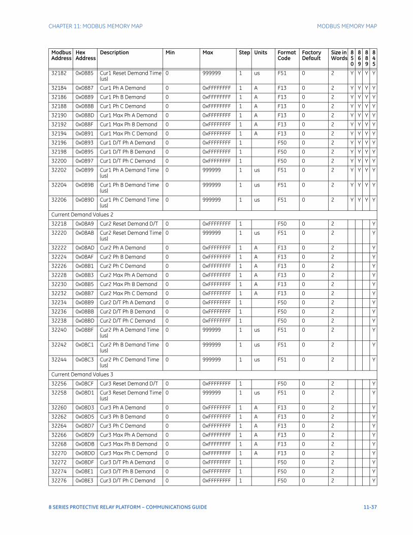
CHAPTER 11: MODBUS MEMORY MAP MODBUS MEMORY MAP
32182 0x0885 Cur1 Reset Demand Time (us)
0 999999 1 us F51 0 2 Y Y Y Y
32184 0x0887 Cur1 Ph A Demand 0 0xFFFFFFFF 1 A F13 0 2 Y Y Y Y
32186 0x0889 Cur1 Ph B Demand 0 0xFFFFFFFF 1 A F13 0 2 Y Y Y Y
32188 0x088B Cur1 Ph C Demand 0 0xFFFFFFFF 1 A F13 0 2 Y Y Y Y
32190 0x088D Cur1 Max Ph A Demand 0 0xFFFFFFFF 1 A F13 0 2 Y Y Y Y
32192 0x088F Cur1 Max Ph B Demand 0 0xFFFFFFFF 1 A F13 0 2 Y Y Y Y
32194 0x0891 Cur1 Max Ph C Demand 0 0xFFFFFFFF 1 A F13 0 2 Y Y Y Y
32196 0x0893 Cur1 D/T Ph A Demand 0 0xFFFFFFFF 1 F50 0 2 Y Y Y Y
32198 0x0895 Cur1 D/T Ph B Demand 0 0xFFFFFFFF 1 F50 0 2 Y Y Y Y
32200 0x0897 Cur1 D/T Ph C Demand 0 0xFFFFFFFF 1 F50 0 2 Y Y Y Y
32202 0x0899 Cur1 Ph A Demand Time (us)
0 999999 1 us F51 0 2 Y Y Y Y
32204 0x089B Cur1 Ph B Demand Time (us)
0 999999 1 us F51 0 2 Y Y Y Y
32206 0x089D Cur1 Ph C Demand Time (us)
0 999999 1 us F51 0 2 Y Y Y Y
Current Demand Values 2
32218 0x08A9 Cur2 Reset Demand D/T 0 0xFFFFFFFF 1 F50 0 2 Y
32220 0x08AB Cur2 Reset Demand Time (us)
0 999999 1 us F51 0 2 Y
32222 0x08AD Cur2 Ph A Demand 0 0xFFFFFFFF 1 A F13 0 2 Y
32224 0x08AF Cur2 Ph B Demand 0 0xFFFFFFFF 1 A F13 0 2 Y
32226 0x08B1 Cur2 Ph C Demand 0 0xFFFFFFFF 1 A F13 0 2 Y
32228 0x08B3 Cur2 Max Ph A Demand 0 0xFFFFFFFF 1 A F13 0 2 Y
32230 0x08B5 Cur2 Max Ph B Demand 0 0xFFFFFFFF 1 A F13 0 2 Y
32232 0x08B7 Cur2 Max Ph C Demand 0 0xFFFFFFFF 1 A F13 0 2 Y
32234 0x08B9 Cur2 D/T Ph A Demand 0 0xFFFFFFFF 1 F50 0 2 Y
32236 0x08BB Cur2 D/T Ph B Demand 0 0xFFFFFFFF 1 F50 0 2 Y
32238 0x08BD Cur2 D/T Ph C Demand 0 0xFFFFFFFF 1 F50 0 2 Y
32240 0x08BF Cur2 Ph A Demand Time (us)
0 999999 1 us F51 0 2 Y
32242 0x08C1 Cur2 Ph B Demand Time (us)
0 999999 1 us F51 0 2 Y
32244 0x08C3 Cur2 Ph C Demand Time (us)
0 999999 1 us F51 0 2 Y
Current Demand Values 3
32256 0x08CF Cur3 Reset Demand D/T 0 0xFFFFFFFF 1 F50 0 2 Y
32258 0x08D1 Cur3 Reset Demand Time (us)
0 999999 1 us F51 0 2 Y
32260 0x08D3 Cur3 Ph A Demand 0 0xFFFFFFFF 1 A F13 0 2 Y
32262 0x08D5 Cur3 Ph B Demand 0 0xFFFFFFFF 1 A F13 0 2 Y
32264 0x08D7 Cur3 Ph C Demand 0 0xFFFFFFFF 1 A F13 0 2 Y
32266 0x08D9 Cur3 Max Ph A Demand 0 0xFFFFFFFF 1 A F13 0 2 Y
32268 0x08DB Cur3 Max Ph B Demand 0 0xFFFFFFFF 1 A F13 0 2 Y
32270 0x08DD Cur3 Max Ph C Demand 0 0xFFFFFFFF 1 A F13 0 2 Y
32272 0x08DF Cur3 D/T Ph A Demand 0 0xFFFFFFFF 1 F50 0 2 Y
32274 0x08E1 Cur3 D/T Ph B Demand 0 0xFFFFFFFF 1 F50 0 2 Y
32276 0x08E3 Cur3 D/T Ph C Demand 0 0xFFFFFFFF 1 F50 0 2 Y
Modbus Address
Hex Address
Description Min Max Step Units Format Code
Factory Default
Size in Words
850
869
889
845
8 SERIES PROTECTIVE RELAY PLATFORM – COMMUNICATIONS GUIDE 11-37
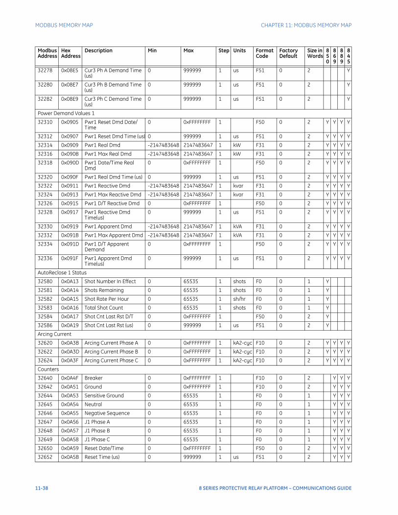
MODBUS MEMORY MAP CHAPTER 11: MODBUS MEMORY MAP
32278 0x08E5 Cur3 Ph A Demand Time (us)
0 999999 1 us F51 0 2 Y
32280 0x08E7 Cur3 Ph B Demand Time (us)
0 999999 1 us F51 0 2 Y
32282 0x08E9 Cur3 Ph C Demand Time (us)
0 999999 1 us F51 0 2 Y
Power Demand Values 1
32310 0x0905 Pwr1 Reset Dmd Date/Time
0 0xFFFFFFFF 1 F50 0 2 Y Y Y Y
32312 0x0907 Pwr1 Reset Dmd Time (us) 0 999999 1 us F51 0 2 Y Y Y Y
32314 0x0909 Pwr1 Real Dmd -2147483648 2147483647 1 kW F31 0 2 Y Y Y Y
32316 0x090B Pwr1 Max Real Dmd -2147483648 2147483647 1 kW F31 0 2 Y Y Y Y
32318 0x090D Pwr1 Date/Time Real Dmd
0 0xFFFFFFFF 1 F50 0 2 Y Y Y Y
32320 0x090F Pwr1 Real Dmd Time (us) 0 999999 1 us F51 0 2 Y Y Y Y
32322 0x0911 Pwr1 Reactive Dmd -2147483648 2147483647 1 kvar F31 0 2 Y Y Y Y
32324 0x0913 Pwr1 Max Reactive Dmd -2147483648 2147483647 1 kvar F31 0 2 Y Y Y Y
32326 0x0915 Pwr1 D/T Reactive Dmd 0 0xFFFFFFFF 1 F50 0 2 Y Y Y Y
32328 0x0917 Pwr1 Reactive Dmd Time(us)
0 999999 1 us F51 0 2 Y Y Y Y
32330 0x0919 Pwr1 Apparent Dmd -2147483648 2147483647 1 kVA F31 0 2 Y Y Y Y
32332 0x091B Pwr1 Max Apparent Dmd -2147483648 2147483647 1 kVA F31 0 2 Y Y Y Y
32334 0x091D Pwr1 D/T Apparent Demand
0 0xFFFFFFFF 1 F50 0 2 Y Y Y Y
32336 0x091F Pwr1 Apparent Dmd Time(us)
0 999999 1 us F51 0 2 Y Y Y Y
AutoReclose 1 Status
32580 0x0A13 Shot Number In Effect 0 65535 1 shots F0 0 1 Y
32581 0x0A14 Shots Remaining 0 65535 1 shots F0 0 1 Y
32582 0x0A15 Shot Rate Per Hour 0 65535 1 sh/hr F0 0 1 Y
32583 0x0A16 Total Shot Count 0 65535 1 shots F0 0 1 Y
32584 0x0A17 Shot Cnt Last Rst D/T 0 0xFFFFFFFF 1 F50 0 2 Y
32586 0x0A19 Shot Cnt Last Rst (us) 0 999999 1 us F51 0 2 Y
Arcing Current
32620 0x0A3B Arcing Current Phase A 0 0xFFFFFFFF 1 kA2-cyc F10 0 2 Y Y Y Y
32622 0x0A3D Arcing Current Phase B 0 0xFFFFFFFF 1 kA2-cyc F10 0 2 Y Y Y Y
32624 0x0A3F Arcing Current Phase C 0 0xFFFFFFFF 1 kA2-cyc F10 0 2 Y Y Y Y
Counters
32640 0x0A4F Breaker 0 0xFFFFFFFF 1 F10 0 2 Y Y Y
32642 0x0A51 Ground 0 0xFFFFFFFF 1 F10 0 2 Y Y Y
32644 0x0A53 Sensitive Ground 0 65535 1 F0 0 1 Y Y Y
32645 0x0A54 Neutral 0 65535 1 F0 0 1 Y Y Y
32646 0x0A55 Negative Sequence 0 65535 1 F0 0 1 Y Y Y
32647 0x0A56 J1 Phase A 0 65535 1 F0 0 1 Y Y Y
32648 0x0A57 J1 Phase B 0 65535 1 F0 0 1 Y Y Y
32649 0x0A58 J1 Phase C 0 65535 1 F0 0 1 Y Y Y
32650 0x0A59 Reset Date/Time 0 0xFFFFFFFF 1 F50 0 2 Y Y Y
32652 0x0A5B Reset Time (us) 0 999999 1 us F51 0 2 Y Y Y
Modbus Address
Hex Address
Description Min Max Step Units Format Code
Factory Default
Size in Words
850
869
889
845
11-38 8 SERIES PROTECTIVE RELAY PLATFORM – COMMUNICATIONS GUIDE
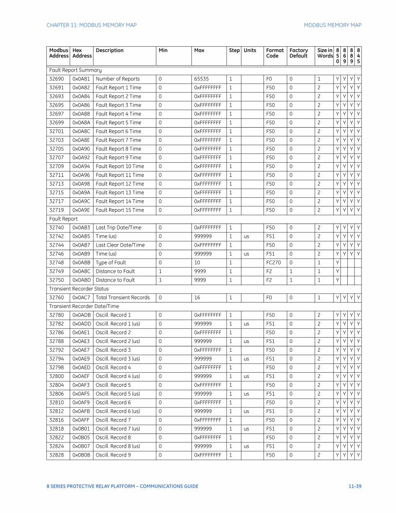
CHAPTER 11: MODBUS MEMORY MAP MODBUS MEMORY MAP
Fault Report Summary
32690 0x0A81 Number of Reports 0 65535 1 F0 0 1 Y Y Y Y
32691 0x0A82 Fault Report 1 Time 0 0xFFFFFFFF 1 F50 0 2 Y Y Y Y
32693 0x0A84 Fault Report 2 Time 0 0xFFFFFFFF 1 F50 0 2 Y Y Y Y
32695 0x0A86 Fault Report 3 Time 0 0xFFFFFFFF 1 F50 0 2 Y Y Y Y
32697 0x0A88 Fault Report 4 Time 0 0xFFFFFFFF 1 F50 0 2 Y Y Y Y
32699 0x0A8A Fault Report 5 Time 0 0xFFFFFFFF 1 F50 0 2 Y Y Y Y
32701 0x0A8C Fault Report 6 Time 0 0xFFFFFFFF 1 F50 0 2 Y Y Y Y
32703 0x0A8E Fault Report 7 Time 0 0xFFFFFFFF 1 F50 0 2 Y Y Y Y
32705 0x0A90 Fault Report 8 Time 0 0xFFFFFFFF 1 F50 0 2 Y Y Y Y
32707 0x0A92 Fault Report 9 Time 0 0xFFFFFFFF 1 F50 0 2 Y Y Y Y
32709 0x0A94 Fault Report 10 Time 0 0xFFFFFFFF 1 F50 0 2 Y Y Y Y
32711 0x0A96 Fault Report 11 Time 0 0xFFFFFFFF 1 F50 0 2 Y Y Y Y
32713 0x0A98 Fault Report 12 Time 0 0xFFFFFFFF 1 F50 0 2 Y Y Y Y
32715 0x0A9A Fault Report 13 Time 0 0xFFFFFFFF 1 F50 0 2 Y Y Y Y
32717 0x0A9C Fault Report 14 Time 0 0xFFFFFFFF 1 F50 0 2 Y Y Y Y
32719 0x0A9E Fault Report 15 Time 0 0xFFFFFFFF 1 F50 0 2 Y Y Y Y
Fault Report
32740 0x0AB3 Last Trip Date/Time 0 0xFFFFFFFF 1 F50 0 2 Y Y Y Y
32742 0x0AB5 Time (us) 0 999999 1 us F51 0 2 Y Y Y Y
32744 0x0AB7 Last Clear Date/Time 0 0xFFFFFFFF 1 F50 0 2 Y Y Y Y
32746 0x0AB9 Time (us) 0 999999 1 us F51 0 2 Y Y Y Y
32748 0x0ABB Type of Fault 0 10 1 FC270 0 1 Y
32749 0x0ABC Distance to Fault 1 9999 1 F2 1 1 Y
32750 0x0ABD Distance to Fault 1 9999 1 F2 1 1 Y
Transient Recorder Status
32760 0x0AC7 Total Transient Records 0 16 1 F0 0 1 Y Y Y Y
Transient Recorder Date/Time
32780 0x0ADB Oscill. Record 1 0 0xFFFFFFFF 1 F50 0 2 Y Y Y Y
32782 0x0ADD Oscill. Record 1 (us) 0 999999 1 us F51 0 2 Y Y Y Y
32786 0x0AE1 Oscill. Record 2 0 0xFFFFFFFF 1 F50 0 2 Y Y Y Y
32788 0x0AE3 Oscill. Record 2 (us) 0 999999 1 us F51 0 2 Y Y Y Y
32792 0x0AE7 Oscill. Record 3 0 0xFFFFFFFF 1 F50 0 2 Y Y Y Y
32794 0x0AE9 Oscill. Record 3 (us) 0 999999 1 us F51 0 2 Y Y Y Y
32798 0x0AED Oscill. Record 4 0 0xFFFFFFFF 1 F50 0 2 Y Y Y Y
32800 0x0AEF Oscill. Record 4 (us) 0 999999 1 us F51 0 2 Y Y Y Y
32804 0x0AF3 Oscill. Record 5 0 0xFFFFFFFF 1 F50 0 2 Y Y Y Y
32806 0x0AF5 Oscill. Record 5 (us) 0 999999 1 us F51 0 2 Y Y Y Y
32810 0x0AF9 Oscill. Record 6 0 0xFFFFFFFF 1 F50 0 2 Y Y Y Y
32812 0x0AFB Oscill. Record 6 (us) 0 999999 1 us F51 0 2 Y Y Y Y
32816 0x0AFF Oscill. Record 7 0 0xFFFFFFFF 1 F50 0 2 Y Y Y Y
32818 0x0B01 Oscill. Record 7 (us) 0 999999 1 us F51 0 2 Y Y Y Y
32822 0x0B05 Oscill. Record 8 0 0xFFFFFFFF 1 F50 0 2 Y Y Y Y
32824 0x0B07 Oscill. Record 8 (us) 0 999999 1 us F51 0 2 Y Y Y Y
32828 0x0B0B Oscill. Record 9 0 0xFFFFFFFF 1 F50 0 2 Y Y Y Y
Modbus Address
Hex Address
Description Min Max Step Units Format Code
Factory Default
Size in Words
850
869
889
845
8 SERIES PROTECTIVE RELAY PLATFORM – COMMUNICATIONS GUIDE 11-39
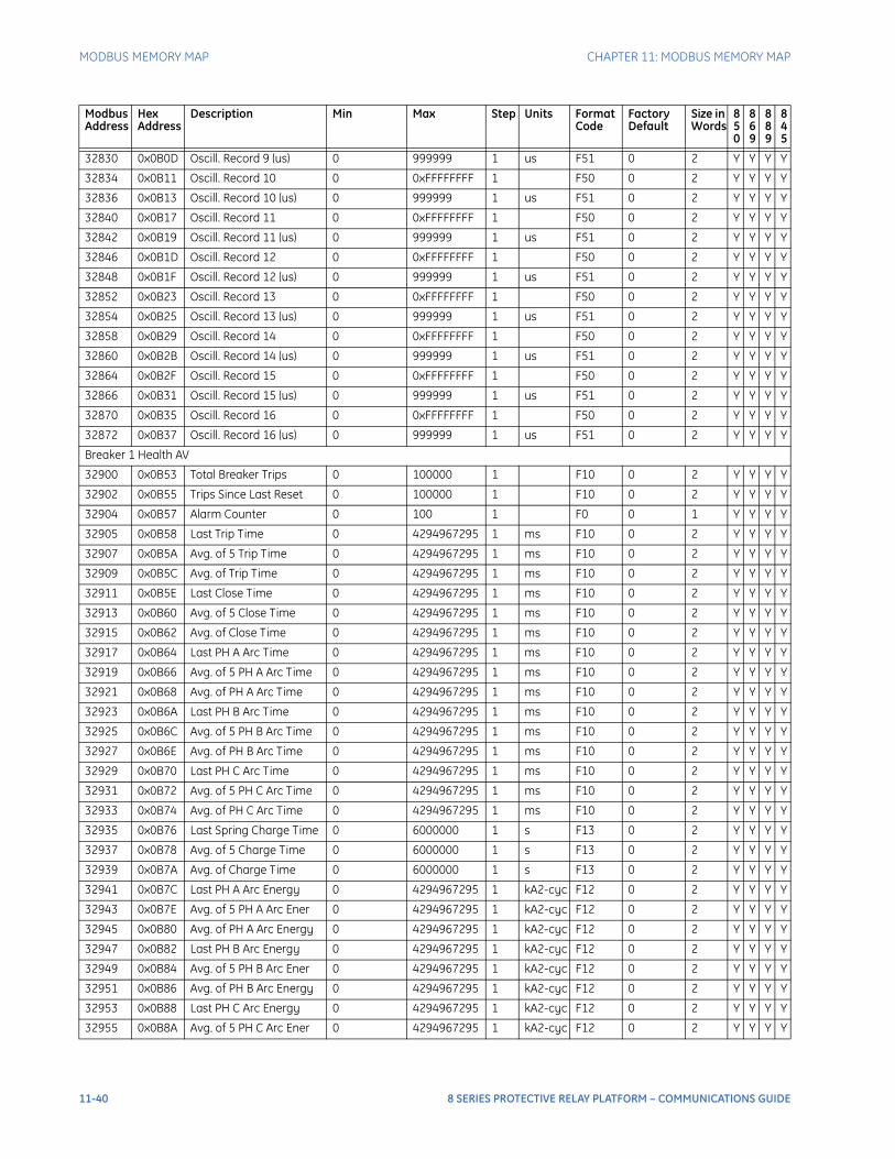
MODBUS MEMORY MAP CHAPTER 11: MODBUS MEMORY MAP
32830 0x0B0D Oscill. Record 9 (us) 0 999999 1 us F51 0 2 Y Y Y Y
32834 0x0B11 Oscill. Record 10 0 0xFFFFFFFF 1 F50 0 2 Y Y Y Y
32836 0x0B13 Oscill. Record 10 (us) 0 999999 1 us F51 0 2 Y Y Y Y
32840 0x0B17 Oscill. Record 11 0 0xFFFFFFFF 1 F50 0 2 Y Y Y Y
32842 0x0B19 Oscill. Record 11 (us) 0 999999 1 us F51 0 2 Y Y Y Y
32846 0x0B1D Oscill. Record 12 0 0xFFFFFFFF 1 F50 0 2 Y Y Y Y
32848 0x0B1F Oscill. Record 12 (us) 0 999999 1 us F51 0 2 Y Y Y Y
32852 0x0B23 Oscill. Record 13 0 0xFFFFFFFF 1 F50 0 2 Y Y Y Y
32854 0x0B25 Oscill. Record 13 (us) 0 999999 1 us F51 0 2 Y Y Y Y
32858 0x0B29 Oscill. Record 14 0 0xFFFFFFFF 1 F50 0 2 Y Y Y Y
32860 0x0B2B Oscill. Record 14 (us) 0 999999 1 us F51 0 2 Y Y Y Y
32864 0x0B2F Oscill. Record 15 0 0xFFFFFFFF 1 F50 0 2 Y Y Y Y
32866 0x0B31 Oscill. Record 15 (us) 0 999999 1 us F51 0 2 Y Y Y Y
32870 0x0B35 Oscill. Record 16 0 0xFFFFFFFF 1 F50 0 2 Y Y Y Y
32872 0x0B37 Oscill. Record 16 (us) 0 999999 1 us F51 0 2 Y Y Y Y
Breaker 1 Health AV
32900 0x0B53 Total Breaker Trips 0 100000 1 F10 0 2 Y Y Y Y
32902 0x0B55 Trips Since Last Reset 0 100000 1 F10 0 2 Y Y Y Y
32904 0x0B57 Alarm Counter 0 100 1 F0 0 1 Y Y Y Y
32905 0x0B58 Last Trip Time 0 4294967295 1 ms F10 0 2 Y Y Y Y
32907 0x0B5A Avg. of 5 Trip Time 0 4294967295 1 ms F10 0 2 Y Y Y Y
32909 0x0B5C Avg. of Trip Time 0 4294967295 1 ms F10 0 2 Y Y Y Y
32911 0x0B5E Last Close Time 0 4294967295 1 ms F10 0 2 Y Y Y Y
32913 0x0B60 Avg. of 5 Close Time 0 4294967295 1 ms F10 0 2 Y Y Y Y
32915 0x0B62 Avg. of Close Time 0 4294967295 1 ms F10 0 2 Y Y Y Y
32917 0x0B64 Last PH A Arc Time 0 4294967295 1 ms F10 0 2 Y Y Y Y
32919 0x0B66 Avg. of 5 PH A Arc Time 0 4294967295 1 ms F10 0 2 Y Y Y Y
32921 0x0B68 Avg. of PH A Arc Time 0 4294967295 1 ms F10 0 2 Y Y Y Y
32923 0x0B6A Last PH B Arc Time 0 4294967295 1 ms F10 0 2 Y Y Y Y
32925 0x0B6C Avg. of 5 PH B Arc Time 0 4294967295 1 ms F10 0 2 Y Y Y Y
32927 0x0B6E Avg. of PH B Arc Time 0 4294967295 1 ms F10 0 2 Y Y Y Y
32929 0x0B70 Last PH C Arc Time 0 4294967295 1 ms F10 0 2 Y Y Y Y
32931 0x0B72 Avg. of 5 PH C Arc Time 0 4294967295 1 ms F10 0 2 Y Y Y Y
32933 0x0B74 Avg. of PH C Arc Time 0 4294967295 1 ms F10 0 2 Y Y Y Y
32935 0x0B76 Last Spring Charge Time 0 6000000 1 s F13 0 2 Y Y Y Y
32937 0x0B78 Avg. of 5 Charge Time 0 6000000 1 s F13 0 2 Y Y Y Y
32939 0x0B7A Avg. of Charge Time 0 6000000 1 s F13 0 2 Y Y Y Y
32941 0x0B7C Last PH A Arc Energy 0 4294967295 1 kA2-cyc F12 0 2 Y Y Y Y
32943 0x0B7E Avg. of 5 PH A Arc Ener 0 4294967295 1 kA2-cyc F12 0 2 Y Y Y Y
32945 0x0B80 Avg. of PH A Arc Energy 0 4294967295 1 kA2-cyc F12 0 2 Y Y Y Y
32947 0x0B82 Last PH B Arc Energy 0 4294967295 1 kA2-cyc F12 0 2 Y Y Y Y
32949 0x0B84 Avg. of 5 PH B Arc Ener 0 4294967295 1 kA2-cyc F12 0 2 Y Y Y Y
32951 0x0B86 Avg. of PH B Arc Energy 0 4294967295 1 kA2-cyc F12 0 2 Y Y Y Y
32953 0x0B88 Last PH C Arc Energy 0 4294967295 1 kA2-cyc F12 0 2 Y Y Y Y
32955 0x0B8A Avg. of 5 PH C Arc Ener 0 4294967295 1 kA2-cyc F12 0 2 Y Y Y Y
Modbus Address
Hex Address
Description Min Max Step Units Format Code
Factory Default
Size in Words
850
869
889
845
11-40 8 SERIES PROTECTIVE RELAY PLATFORM – COMMUNICATIONS GUIDE
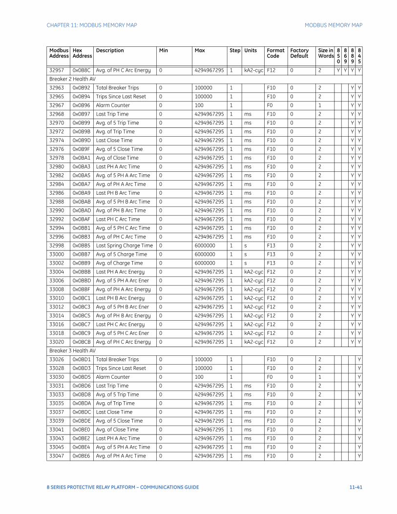
CHAPTER 11: MODBUS MEMORY MAP MODBUS MEMORY MAP
32957 0x0B8C Avg. of PH C Arc Energy 0 4294967295 1 kA2-cyc F12 0 2 Y Y Y Y
Breaker 2 Health AV
32963 0x0B92 Total Breaker Trips 0 100000 1 F10 0 2 Y Y
32965 0x0B94 Trips Since Last Reset 0 100000 1 F10 0 2 Y Y
32967 0x0B96 Alarm Counter 0 100 1 F0 0 1 Y Y
32968 0x0B97 Last Trip Time 0 4294967295 1 ms F10 0 2 Y Y
32970 0x0B99 Avg. of 5 Trip Time 0 4294967295 1 ms F10 0 2 Y Y
32972 0x0B9B Avg. of Trip Time 0 4294967295 1 ms F10 0 2 Y Y
32974 0x0B9D Last Close Time 0 4294967295 1 ms F10 0 2 Y Y
32976 0x0B9F Avg. of 5 Close Time 0 4294967295 1 ms F10 0 2 Y Y
32978 0x0BA1 Avg. of Close Time 0 4294967295 1 ms F10 0 2 Y Y
32980 0x0BA3 Last PH A Arc Time 0 4294967295 1 ms F10 0 2 Y Y
32982 0x0BA5 Avg. of 5 PH A Arc Time 0 4294967295 1 ms F10 0 2 Y Y
32984 0x0BA7 Avg. of PH A Arc Time 0 4294967295 1 ms F10 0 2 Y Y
32986 0x0BA9 Last PH B Arc Time 0 4294967295 1 ms F10 0 2 Y Y
32988 0x0BAB Avg. of 5 PH B Arc Time 0 4294967295 1 ms F10 0 2 Y Y
32990 0x0BAD Avg. of PH B Arc Time 0 4294967295 1 ms F10 0 2 Y Y
32992 0x0BAF Last PH C Arc Time 0 4294967295 1 ms F10 0 2 Y Y
32994 0x0BB1 Avg. of 5 PH C Arc Time 0 4294967295 1 ms F10 0 2 Y Y
32996 0x0BB3 Avg. of PH C Arc Time 0 4294967295 1 ms F10 0 2 Y Y
32998 0x0BB5 Last Spring Charge Time 0 6000000 1 s F13 0 2 Y Y
33000 0x0BB7 Avg. of 5 Charge Time 0 6000000 1 s F13 0 2 Y Y
33002 0x0BB9 Avg. of Charge Time 0 6000000 1 s F13 0 2 Y Y
33004 0x0BBB Last PH A Arc Energy 0 4294967295 1 kA2-cyc F12 0 2 Y Y
33006 0x0BBD Avg. of 5 PH A Arc Ener 0 4294967295 1 kA2-cyc F12 0 2 Y Y
33008 0x0BBF Avg. of PH A Arc Energy 0 4294967295 1 kA2-cyc F12 0 2 Y Y
33010 0x0BC1 Last PH B Arc Energy 0 4294967295 1 kA2-cyc F12 0 2 Y Y
33012 0x0BC3 Avg. of 5 PH B Arc Ener 0 4294967295 1 kA2-cyc F12 0 2 Y Y
33014 0x0BC5 Avg. of PH B Arc Energy 0 4294967295 1 kA2-cyc F12 0 2 Y Y
33016 0x0BC7 Last PH C Arc Energy 0 4294967295 1 kA2-cyc F12 0 2 Y Y
33018 0x0BC9 Avg. of 5 PH C Arc Ener 0 4294967295 1 kA2-cyc F12 0 2 Y Y
33020 0x0BCB Avg. of PH C Arc Energy 0 4294967295 1 kA2-cyc F12 0 2 Y Y
Breaker 3 Health AV
33026 0x0BD1 Total Breaker Trips 0 100000 1 F10 0 2 Y
33028 0x0BD3 Trips Since Last Reset 0 100000 1 F10 0 2 Y
33030 0x0BD5 Alarm Counter 0 100 1 F0 0 1 Y
33031 0x0BD6 Last Trip Time 0 4294967295 1 ms F10 0 2 Y
33033 0x0BD8 Avg. of 5 Trip Time 0 4294967295 1 ms F10 0 2 Y
33035 0x0BDA Avg. of Trip Time 0 4294967295 1 ms F10 0 2 Y
33037 0x0BDC Last Close Time 0 4294967295 1 ms F10 0 2 Y
33039 0x0BDE Avg. of 5 Close Time 0 4294967295 1 ms F10 0 2 Y
33041 0x0BE0 Avg. of Close Time 0 4294967295 1 ms F10 0 2 Y
33043 0x0BE2 Last PH A Arc Time 0 4294967295 1 ms F10 0 2 Y
33045 0x0BE4 Avg. of 5 PH A Arc Time 0 4294967295 1 ms F10 0 2 Y
33047 0x0BE6 Avg. of PH A Arc Time 0 4294967295 1 ms F10 0 2 Y
Modbus Address
Hex Address
Description Min Max Step Units Format Code
Factory Default
Size in Words
850
869
889
845
8 SERIES PROTECTIVE RELAY PLATFORM – COMMUNICATIONS GUIDE 11-41
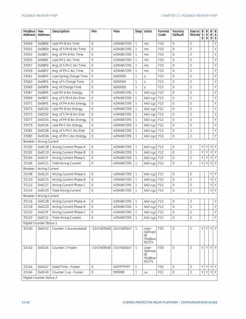
MODBUS MEMORY MAP CHAPTER 11: MODBUS MEMORY MAP
33049 0x0BE8 Last PH B Arc Time 0 4294967295 1 ms F10 0 2 Y
33051 0x0BEA Avg. of 5 PH B Arc Time 0 4294967295 1 ms F10 0 2 Y
33053 0x0BEC Avg. of PH B Arc Time 0 4294967295 1 ms F10 0 2 Y
33055 0x0BEE Last PH C Arc Time 0 4294967295 1 ms F10 0 2 Y
33057 0x0BF0 Avg. of 5 PH C Arc Time 0 4294967295 1 ms F10 0 2 Y
33059 0x0BF2 Avg. of PH C Arc Time 0 4294967295 1 ms F10 0 2 Y
33061 0x0BF4 Last Spring Charge Time 0 6000000 1 s F13 0 2 Y
33063 0x0BF6 Avg. of 5 Charge Time 0 6000000 1 s F13 0 2 Y
33065 0x0BF8 Avg. of Charge Time 0 6000000 1 s F13 0 2 Y
33067 0x0BFA Last PH A Arc Energy 0 4294967295 1 kA2-cyc F12 0 2 Y
33069 0x0BFC Avg. of 5 PH A Arc Ener 0 4294967295 1 kA2-cyc F12 0 2 Y
33071 0x0BFE Avg. of PH A Arc Energy 0 4294967295 1 kA2-cyc F12 0 2 Y
33073 0x0C00 Last PH B Arc Energy 0 4294967295 1 kA2-cyc F12 0 2 Y
33075 0x0C02 Avg. of 5 PH B Arc Ener 0 4294967295 1 kA2-cyc F12 0 2 Y
33077 0x0C04 Avg. of PH B Arc Energy 0 4294967295 1 kA2-cyc F12 0 2 Y
33079 0x0C06 Last PH C Arc Energy 0 4294967295 1 kA2-cyc F12 0 2 Y
33081 0x0C08 Avg. of 5 PH C Arc Ener 0 4294967295 1 kA2-cyc F12 0 2 Y
33083 0x0C0A Avg. of PH C Arc Energy 0 4294967295 1 kA2-cyc F12 0 2 Y
Breaker 1 Arcing Current
33100 0x0C1B Arcing Current Phase A 0 4294967295 1 kA2-cyc F12 0 2 Y Y Y Y
33102 0x0C1D Arcing Current Phase B 0 4294967295 1 kA2-cyc F12 0 2 Y Y Y Y
33104 0x0C1F Arcing Current Phase C 0 4294967295 1 kA2-cyc F12 0 2 Y Y Y Y
33106 0x0C21 Total Arcing Current 0 4294967295 1 kA2-cyc F12 0 2 Y Y Y Y
Breaker 2 Arcing Current
33108 0x0C23 Arcing Current Phase A 0 4294967295 1 kA2-cyc F12 0 2 Y Y
33110 0x0C25 Arcing Current Phase B 0 4294967295 1 kA2-cyc F12 0 2 Y Y
33112 0x0C27 Arcing Current Phase C 0 4294967295 1 kA2-cyc F12 0 2 Y Y
33114 0x0C29 Total Arcing Current 0 4294967295 1 kA2-cyc F12 0 2 Y Y
Breaker 3 Arcing Current
33116 0x0C2B Arcing Current Phase A 0 4294967295 1 kA2-cyc F12 0 2 Y
33118 0x0C2D Arcing Current Phase B 0 4294967295 1 kA2-cyc F12 0 2 Y
33120 0x0C2F Arcing Current Phase C 0 4294967295 1 kA2-cyc F12 0 2 Y
33122 0x0C31 Total Arcing Current 0 4294967295 1 kA2-cyc F12 0 2 Y
Digital Counter Status 1
33140 0x0C43 Counter 1 Accumulated -2147483648 2147483647 1 User-Defined @ Modbus 81374
F30 0 2 Y Y Y Y
33142 0x0C45 Counter 1 Frozen -2147483648 2147483647 1 User-Defined @ Modbus 81374
F30 0 2 Y Y Y Y
33144 0x0C47 Date/Time - Frozen 0 0xFFFFFFFF 1 F50 0 2 Y Y Y Y
33146 0x0C49 Counter 1 us - Frozen 0 999999 1 us F51 0 2 Y Y Y Y
Digital Counter Status 2
Modbus Address
Hex Address
Description Min Max Step Units Format Code
Factory Default
Size in Words
850
869
889
845
11-42 8 SERIES PROTECTIVE RELAY PLATFORM – COMMUNICATIONS GUIDE

CHAPTER 11: MODBUS MEMORY MAP MODBUS MEMORY MAP
33152 0x0C4F Counter 2 Accumulated -2147483648 2147483647 1 User-Defined @ Modbus 81416
F30 0 2 Y Y Y Y
33154 0x0C51 Counter 2 Frozen -2147483648 2147483647 1 User-Defined @ Modbus 81416
F30 0 2 Y Y Y Y
33156 0x0C53 Date/Time - Frozen 0 0xFFFFFFFF 1 F50 0 2 Y Y Y Y
33158 0x0C55 Counter 2 us - Frozen 0 999999 1 us F51 0 2 Y Y Y Y
Digital Counter Status 3
33164 0x0C5B Counter 3 Accumulated -2147483648 2147483647 1 User-Defined @ Modbus 81458
F30 0 2 Y Y Y Y
33166 0x0C5D Counter 3 Frozen -2147483648 2147483647 1 User-Defined @ Modbus 81458
F30 0 2 Y Y Y Y
33168 0x0C5F Date/Time - Frozen 0 0xFFFFFFFF 1 F50 0 2 Y Y Y Y
33170 0x0C61 Counter 3 us - Frozen 0 999999 1 us F51 0 2 Y Y Y Y
Digital Counter Status 4
33176 0x0C67 Counter 4 Accumulated -2147483648 2147483647 1 User-Defined @ Modbus 81500
F30 0 2 Y Y Y Y
33178 0x0C69 Counter 4 Frozen -2147483648 2147483647 1 User-Defined @ Modbus 81500
F30 0 2 Y Y Y Y
33180 0x0C6B Date/Time - Frozen 0 0xFFFFFFFF 1 F50 0 2 Y Y Y Y
33182 0x0C6D Counter 4 us - Frozen 0 999999 1 us F51 0 2 Y Y Y Y
Digital Counter Status 5
33188 0x0C73 Counter 5 Accumulated -2147483648 2147483647 1 User-Defined @ Modbus 81542
F30 0 2 Y Y Y Y
33190 0x0C75 Counter 5 Frozen -2147483648 2147483647 1 User-Defined @ Modbus 81542
F30 0 2 Y Y Y Y
33192 0x0C77 Date/Time - Frozen 0 0xFFFFFFFF 1 F50 0 2 Y Y Y Y
33194 0x0C79 Counter 5 us - Frozen 0 999999 1 us F51 0 2 Y Y Y Y
Digital Counter Status 6
33200 0x0C7F Counter 6 Accumulated -2147483648 2147483647 1 User-Defined @ Modbus 81584
F30 0 2 Y Y Y Y
Modbus Address
Hex Address
Description Min Max Step Units Format Code
Factory Default
Size in Words
850
869
889
845
8 SERIES PROTECTIVE RELAY PLATFORM – COMMUNICATIONS GUIDE 11-43
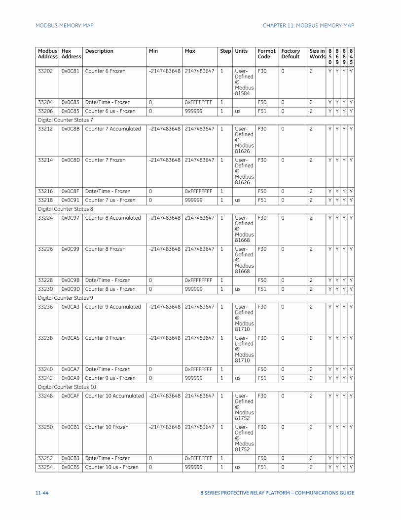
MODBUS MEMORY MAP CHAPTER 11: MODBUS MEMORY MAP
33202 0x0C81 Counter 6 Frozen -2147483648 2147483647 1 User-Defined @ Modbus 81584
F30 0 2 Y Y Y Y
33204 0x0C83 Date/Time - Frozen 0 0xFFFFFFFF 1 F50 0 2 Y Y Y Y
33206 0x0C85 Counter 6 us - Frozen 0 999999 1 us F51 0 2 Y Y Y Y
Digital Counter Status 7
33212 0x0C8B Counter 7 Accumulated -2147483648 2147483647 1 User-Defined @ Modbus 81626
F30 0 2 Y Y Y Y
33214 0x0C8D Counter 7 Frozen -2147483648 2147483647 1 User-Defined @ Modbus 81626
F30 0 2 Y Y Y Y
33216 0x0C8F Date/Time - Frozen 0 0xFFFFFFFF 1 F50 0 2 Y Y Y Y
33218 0x0C91 Counter 7 us - Frozen 0 999999 1 us F51 0 2 Y Y Y Y
Digital Counter Status 8
33224 0x0C97 Counter 8 Accumulated -2147483648 2147483647 1 User-Defined @ Modbus 81668
F30 0 2 Y Y Y Y
33226 0x0C99 Counter 8 Frozen -2147483648 2147483647 1 User-Defined @ Modbus 81668
F30 0 2 Y Y Y Y
33228 0x0C9B Date/Time - Frozen 0 0xFFFFFFFF 1 F50 0 2 Y Y Y Y
33230 0x0C9D Counter 8 us - Frozen 0 999999 1 us F51 0 2 Y Y Y Y
Digital Counter Status 9
33236 0x0CA3 Counter 9 Accumulated -2147483648 2147483647 1 User-Defined @ Modbus 81710
F30 0 2 Y Y Y Y
33238 0x0CA5 Counter 9 Frozen -2147483648 2147483647 1 User-Defined @ Modbus 81710
F30 0 2 Y Y Y Y
33240 0x0CA7 Date/Time - Frozen 0 0xFFFFFFFF 1 F50 0 2 Y Y Y Y
33242 0x0CA9 Counter 9 us - Frozen 0 999999 1 us F51 0 2 Y Y Y Y
Digital Counter Status 10
33248 0x0CAF Counter 10 Accumulated -2147483648 2147483647 1 User-Defined @ Modbus 81752
F30 0 2 Y Y Y Y
33250 0x0CB1 Counter 10 Frozen -2147483648 2147483647 1 User-Defined @ Modbus 81752
F30 0 2 Y Y Y Y
33252 0x0CB3 Date/Time - Frozen 0 0xFFFFFFFF 1 F50 0 2 Y Y Y Y
33254 0x0CB5 Counter 10 us - Frozen 0 999999 1 us F51 0 2 Y Y Y Y
Modbus Address
Hex Address
Description Min Max Step Units Format Code
Factory Default
Size in Words
850
869
889
845
11-44 8 SERIES PROTECTIVE RELAY PLATFORM – COMMUNICATIONS GUIDE
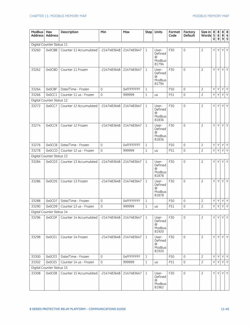
CHAPTER 11: MODBUS MEMORY MAP MODBUS MEMORY MAP
Digital Counter Status 11
33260 0x0CBB Counter 11 Accumulated -2147483648 2147483647 1 User-Defined @ Modbus 81794
F30 0 2 Y Y Y Y
33262 0x0CBD Counter 11 Frozen -2147483648 2147483647 1 User-Defined @ Modbus 81794
F30 0 2 Y Y Y Y
33264 0x0CBF Date/Time - Frozen 0 0xFFFFFFFF 1 F50 0 2 Y Y Y Y
33266 0x0CC1 Counter 11 us - Frozen 0 999999 1 us F51 0 2 Y Y Y Y
Digital Counter Status 12
33272 0x0CC7 Counter 12 Accumulated -2147483648 2147483647 1 User-Defined @ Modbus 81836
F30 0 2 Y Y Y Y
33274 0x0CC9 Counter 12 Frozen -2147483648 2147483647 1 User-Defined @ Modbus 81836
F30 0 2 Y Y Y Y
33276 0x0CCB Date/Time - Frozen 0 0xFFFFFFFF 1 F50 0 2 Y Y Y Y
33278 0x0CCD Counter 12 us - Frozen 0 999999 1 us F51 0 2 Y Y Y Y
Digital Counter Status 13
33284 0x0CD3 Counter 13 Accumulated -2147483648 2147483647 1 User-Defined @ Modbus 81878
F30 0 2 Y Y Y Y
33286 0x0CD5 Counter 13 Frozen -2147483648 2147483647 1 User-Defined @ Modbus 81878
F30 0 2 Y Y Y Y
33288 0x0CD7 Date/Time - Frozen 0 0xFFFFFFFF 1 F50 0 2 Y Y Y Y
33290 0x0CD9 Counter 13 us - Frozen 0 999999 1 us F51 0 2 Y Y Y Y
Digital Counter Status 14
33296 0x0CDF Counter 14 Accumulated -2147483648 2147483647 1 User-Defined @ Modbus 81920
F30 0 2 Y Y Y Y
33298 0x0CE1 Counter 14 Frozen -2147483648 2147483647 1 User-Defined @ Modbus 81920
F30 0 2 Y Y Y Y
33300 0x0CE3 Date/Time - Frozen 0 0xFFFFFFFF 1 F50 0 2 Y Y Y Y
33302 0x0CE5 Counter 14 us - Frozen 0 999999 1 us F51 0 2 Y Y Y Y
Digital Counter Status 15
33308 0x0CEB Counter 15 Accumulated -2147483648 2147483647 1 User-Defined @ Modbus 81962
F30 0 2 Y Y Y Y
Modbus Address
Hex Address
Description Min Max Step Units Format Code
Factory Default
Size in Words
850
869
889
845
8 SERIES PROTECTIVE RELAY PLATFORM – COMMUNICATIONS GUIDE 11-45
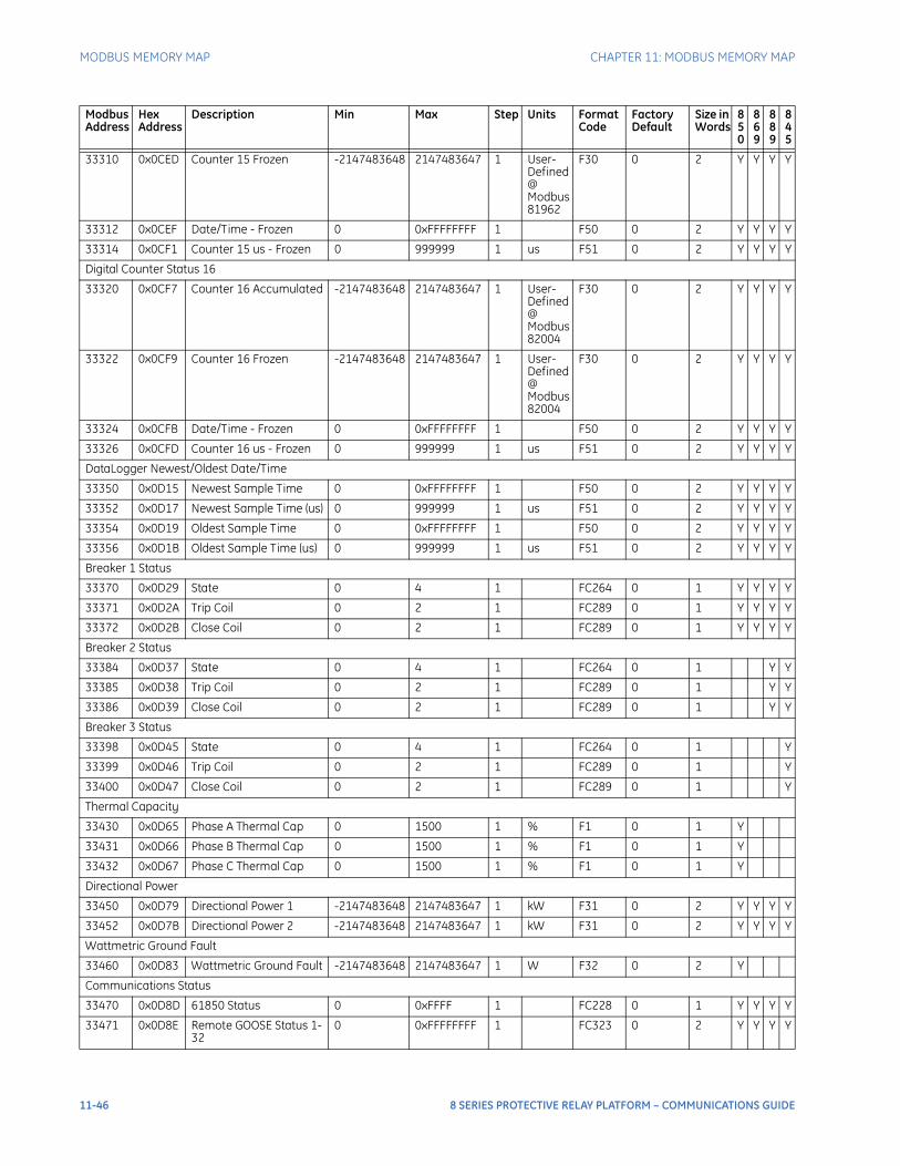
MODBUS MEMORY MAP CHAPTER 11: MODBUS MEMORY MAP
33310 0x0CED Counter 15 Frozen -2147483648 2147483647 1 User-Defined @ Modbus 81962
F30 0 2 Y Y Y Y
33312 0x0CEF Date/Time - Frozen 0 0xFFFFFFFF 1 F50 0 2 Y Y Y Y
33314 0x0CF1 Counter 15 us - Frozen 0 999999 1 us F51 0 2 Y Y Y Y
Digital Counter Status 16
33320 0x0CF7 Counter 16 Accumulated -2147483648 2147483647 1 User-Defined @ Modbus 82004
F30 0 2 Y Y Y Y
33322 0x0CF9 Counter 16 Frozen -2147483648 2147483647 1 User-Defined @ Modbus 82004
F30 0 2 Y Y Y Y
33324 0x0CFB Date/Time - Frozen 0 0xFFFFFFFF 1 F50 0 2 Y Y Y Y
33326 0x0CFD Counter 16 us - Frozen 0 999999 1 us F51 0 2 Y Y Y Y
DataLogger Newest/Oldest Date/Time
33350 0x0D15 Newest Sample Time 0 0xFFFFFFFF 1 F50 0 2 Y Y Y Y
33352 0x0D17 Newest Sample Time (us) 0 999999 1 us F51 0 2 Y Y Y Y
33354 0x0D19 Oldest Sample Time 0 0xFFFFFFFF 1 F50 0 2 Y Y Y Y
33356 0x0D1B Oldest Sample Time (us) 0 999999 1 us F51 0 2 Y Y Y Y
Breaker 1 Status
33370 0x0D29 State 0 4 1 FC264 0 1 Y Y Y Y
33371 0x0D2A Trip Coil 0 2 1 FC289 0 1 Y Y Y Y
33372 0x0D2B Close Coil 0 2 1 FC289 0 1 Y Y Y Y
Breaker 2 Status
33384 0x0D37 State 0 4 1 FC264 0 1 Y Y
33385 0x0D38 Trip Coil 0 2 1 FC289 0 1 Y Y
33386 0x0D39 Close Coil 0 2 1 FC289 0 1 Y Y
Breaker 3 Status
33398 0x0D45 State 0 4 1 FC264 0 1 Y
33399 0x0D46 Trip Coil 0 2 1 FC289 0 1 Y
33400 0x0D47 Close Coil 0 2 1 FC289 0 1 Y
Thermal Capacity
33430 0x0D65 Phase A Thermal Cap 0 1500 1 % F1 0 1 Y
33431 0x0D66 Phase B Thermal Cap 0 1500 1 % F1 0 1 Y
33432 0x0D67 Phase C Thermal Cap 0 1500 1 % F1 0 1 Y
Directional Power
33450 0x0D79 Directional Power 1 -2147483648 2147483647 1 kW F31 0 2 Y Y Y Y
33452 0x0D7B Directional Power 2 -2147483648 2147483647 1 kW F31 0 2 Y Y Y Y
Wattmetric Ground Fault
33460 0x0D83 Wattmetric Ground Fault -2147483648 2147483647 1 W F32 0 2 Y
Communications Status
33470 0x0D8D 61850 Status 0 0xFFFF 1 FC228 0 1 Y Y Y Y
33471 0x0D8E Remote GOOSE Status 1-32
0 0xFFFFFFFF 1 FC323 0 2 Y Y Y Y
Modbus Address
Hex Address
Description Min Max Step Units Format Code
Factory Default
Size in Words
850
869
889
845
11-46 8 SERIES PROTECTIVE RELAY PLATFORM – COMMUNICATIONS GUIDE
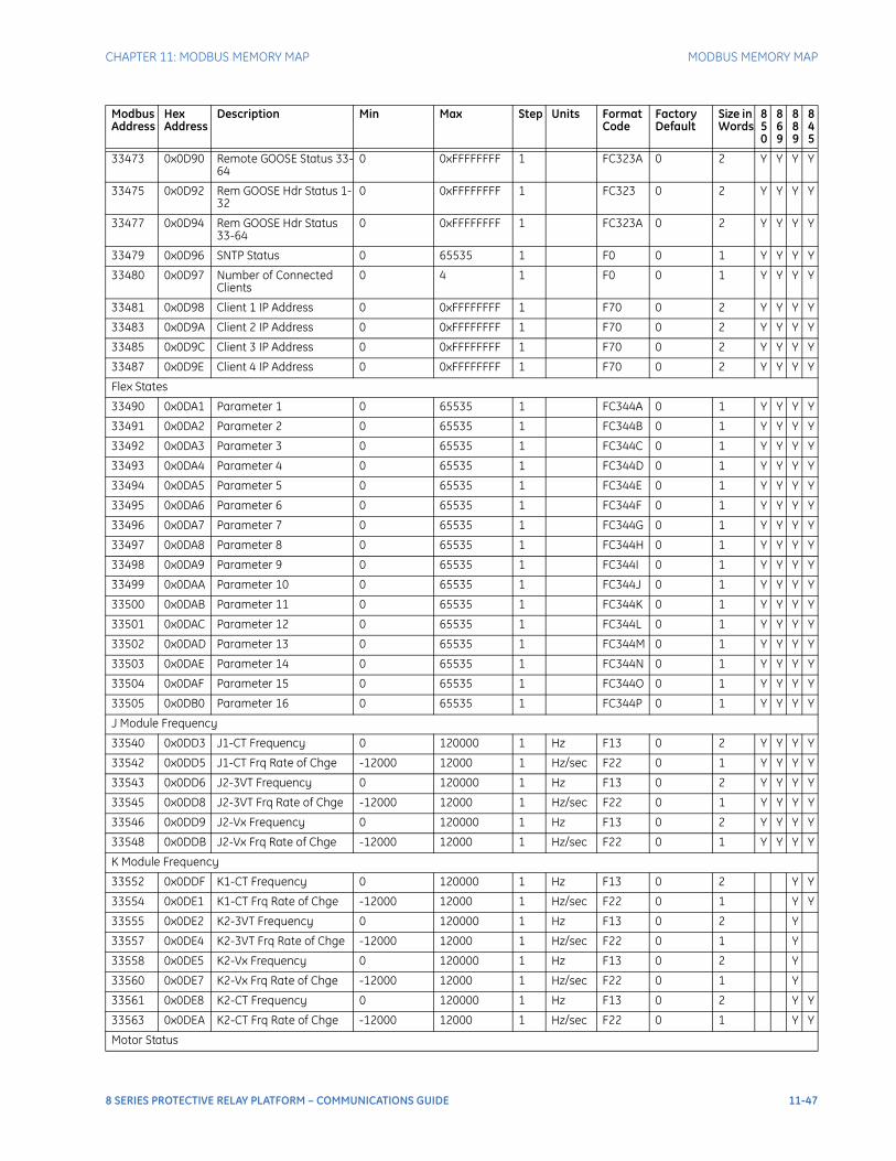
CHAPTER 11: MODBUS MEMORY MAP MODBUS MEMORY MAP
33473 0x0D90 Remote GOOSE Status 33-64
0 0xFFFFFFFF 1 FC323A 0 2 Y Y Y Y
33475 0x0D92 Rem GOOSE Hdr Status 1-32
0 0xFFFFFFFF 1 FC323 0 2 Y Y Y Y
33477 0x0D94 Rem GOOSE Hdr Status 33-64
0 0xFFFFFFFF 1 FC323A 0 2 Y Y Y Y
33479 0x0D96 SNTP Status 0 65535 1 F0 0 1 Y Y Y Y
33480 0x0D97 Number of Connected Clients
0 4 1 F0 0 1 Y Y Y Y
33481 0x0D98 Client 1 IP Address 0 0xFFFFFFFF 1 F70 0 2 Y Y Y Y
33483 0x0D9A Client 2 IP Address 0 0xFFFFFFFF 1 F70 0 2 Y Y Y Y
33485 0x0D9C Client 3 IP Address 0 0xFFFFFFFF 1 F70 0 2 Y Y Y Y
33487 0x0D9E Client 4 IP Address 0 0xFFFFFFFF 1 F70 0 2 Y Y Y Y
Flex States
33490 0x0DA1 Parameter 1 0 65535 1 FC344A 0 1 Y Y Y Y
33491 0x0DA2 Parameter 2 0 65535 1 FC344B 0 1 Y Y Y Y
33492 0x0DA3 Parameter 3 0 65535 1 FC344C 0 1 Y Y Y Y
33493 0x0DA4 Parameter 4 0 65535 1 FC344D 0 1 Y Y Y Y
33494 0x0DA5 Parameter 5 0 65535 1 FC344E 0 1 Y Y Y Y
33495 0x0DA6 Parameter 6 0 65535 1 FC344F 0 1 Y Y Y Y
33496 0x0DA7 Parameter 7 0 65535 1 FC344G 0 1 Y Y Y Y
33497 0x0DA8 Parameter 8 0 65535 1 FC344H 0 1 Y Y Y Y
33498 0x0DA9 Parameter 9 0 65535 1 FC344I 0 1 Y Y Y Y
33499 0x0DAA Parameter 10 0 65535 1 FC344J 0 1 Y Y Y Y
33500 0x0DAB Parameter 11 0 65535 1 FC344K 0 1 Y Y Y Y
33501 0x0DAC Parameter 12 0 65535 1 FC344L 0 1 Y Y Y Y
33502 0x0DAD Parameter 13 0 65535 1 FC344M 0 1 Y Y Y Y
33503 0x0DAE Parameter 14 0 65535 1 FC344N 0 1 Y Y Y Y
33504 0x0DAF Parameter 15 0 65535 1 FC344O 0 1 Y Y Y Y
33505 0x0DB0 Parameter 16 0 65535 1 FC344P 0 1 Y Y Y Y
J Module Frequency
33540 0x0DD3 J1-CT Frequency 0 120000 1 Hz F13 0 2 Y Y Y Y
33542 0x0DD5 J1-CT Frq Rate of Chge -12000 12000 1 Hz/sec F22 0 1 Y Y Y Y
33543 0x0DD6 J2-3VT Frequency 0 120000 1 Hz F13 0 2 Y Y Y Y
33545 0x0DD8 J2-3VT Frq Rate of Chge -12000 12000 1 Hz/sec F22 0 1 Y Y Y Y
33546 0x0DD9 J2-Vx Frequency 0 120000 1 Hz F13 0 2 Y Y Y Y
33548 0x0DDB J2-Vx Frq Rate of Chge -12000 12000 1 Hz/sec F22 0 1 Y Y Y Y
K Module Frequency
33552 0x0DDF K1-CT Frequency 0 120000 1 Hz F13 0 2 Y Y
33554 0x0DE1 K1-CT Frq Rate of Chge -12000 12000 1 Hz/sec F22 0 1 Y Y
33555 0x0DE2 K2-3VT Frequency 0 120000 1 Hz F13 0 2 Y
33557 0x0DE4 K2-3VT Frq Rate of Chge -12000 12000 1 Hz/sec F22 0 1 Y
33558 0x0DE5 K2-Vx Frequency 0 120000 1 Hz F13 0 2 Y
33560 0x0DE7 K2-Vx Frq Rate of Chge -12000 12000 1 Hz/sec F22 0 1 Y
33561 0x0DE8 K2-CT Frequency 0 120000 1 Hz F13 0 2 Y Y
33563 0x0DEA K2-CT Frq Rate of Chge -12000 12000 1 Hz/sec F22 0 1 Y Y
Motor Status
Modbus Address
Hex Address
Description Min Max Step Units Format Code
Factory Default
Size in Words
850
869
889
845
8 SERIES PROTECTIVE RELAY PLATFORM – COMMUNICATIONS GUIDE 11-47
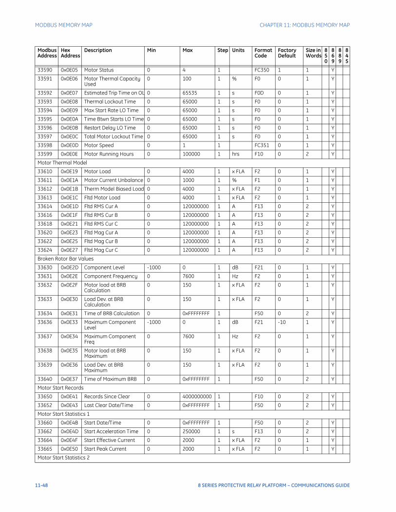
MODBUS MEMORY MAP CHAPTER 11: MODBUS MEMORY MAP
33590 0x0E05 Motor Status 0 4 1 FC350 1 1 Y
33591 0x0E06 Motor Thermal Capacity Used
0 100 1 % F0 0 1 Y
33592 0x0E07 Estimated Trip Time on OL 0 65535 1 s F0D 0 1 Y
33593 0x0E08 Thermal Lockout Time 0 65000 1 s F0 0 1 Y
33594 0x0E09 Max Start Rate LO Time 0 65000 1 s F0 0 1 Y
33595 0x0E0A Time Btwn Starts LO Time 0 65000 1 s F0 0 1 Y
33596 0x0E0B Restart Delay LO Time 0 65000 1 s F0 0 1 Y
33597 0x0E0C Total Motor Lockout Time 0 65000 1 s F0 0 1 Y
33598 0x0E0D Motor Speed 0 1 1 FC351 0 1 Y
33599 0x0E0E Motor Running Hours 0 100000 1 hrs F10 0 2 Y
Motor Thermal Model
33610 0x0E19 Motor Load 0 4000 1 x FLA F2 0 1 Y
33611 0x0E1A Motor Current Unbalance 0 1000 1 % F1 0 1 Y
33612 0x0E1B Therm Model Biased Load 0 4000 1 x FLA F2 0 1 Y
33613 0x0E1C Fltd Motor Load 0 4000 1 x FLA F2 0 1 Y
33614 0x0E1D Fltd RMS Cur A 0 120000000 1 A F13 0 2 Y
33616 0x0E1F Fltd RMS Cur B 0 120000000 1 A F13 0 2 Y
33618 0x0E21 Fltd RMS Cur C 0 120000000 1 A F13 0 2 Y
33620 0x0E23 Fltd Mag Cur A 0 120000000 1 A F13 0 2 Y
33622 0x0E25 Fltd Mag Cur B 0 120000000 1 A F13 0 2 Y
33624 0x0E27 Fltd Mag Cur C 0 120000000 1 A F13 0 2 Y
Broken Rotor Bar Values
33630 0x0E2D Component Level -1000 0 1 dB F21 0 1 Y
33631 0x0E2E Component Frequency 0 7600 1 Hz F2 0 1 Y
33632 0x0E2F Motor load at BRB Calculation
0 150 1 x FLA F2 0 1 Y
33633 0x0E30 Load Dev. at BRB Calculation
0 150 1 x FLA F2 0 1 Y
33634 0x0E31 Time of BRB Calculation 0 0xFFFFFFFF 1 F50 0 2 Y
33636 0x0E33 Maximum Component Level
-1000 0 1 dB F21 -10 1 Y
33637 0x0E34 Maximum Component Freq
0 7600 1 Hz F2 0 1 Y
33638 0x0E35 Motor load at BRB Maximum
0 150 1 x FLA F2 0 1 Y
33639 0x0E36 Load Dev. at BRB Maximum
0 150 1 x FLA F2 0 1 Y
33640 0x0E37 Time of Maximum BRB 0 0xFFFFFFFF 1 F50 0 2 Y
Motor Start Records
33650 0x0E41 Records Since Clear 0 4000000000 1 F10 0 2 Y
33652 0x0E43 Last Clear Date/Time 0 0xFFFFFFFF 1 F50 0 2 Y
Motor Start Statistics 1
33660 0x0E4B Start Date/Time 0 0xFFFFFFFF 1 F50 0 2 Y
33662 0x0E4D Start Acceleration Time 0 250000 1 s F13 0 2 Y
33664 0x0E4F Start Effective Current 0 2000 1 x FLA F2 0 1 Y
33665 0x0E50 Start Peak Current 0 2000 1 x FLA F2 0 1 Y
Motor Start Statistics 2
Modbus Address
Hex Address
Description Min Max Step Units Format Code
Factory Default
Size in Words
850
869
889
845
11-48 8 SERIES PROTECTIVE RELAY PLATFORM – COMMUNICATIONS GUIDE
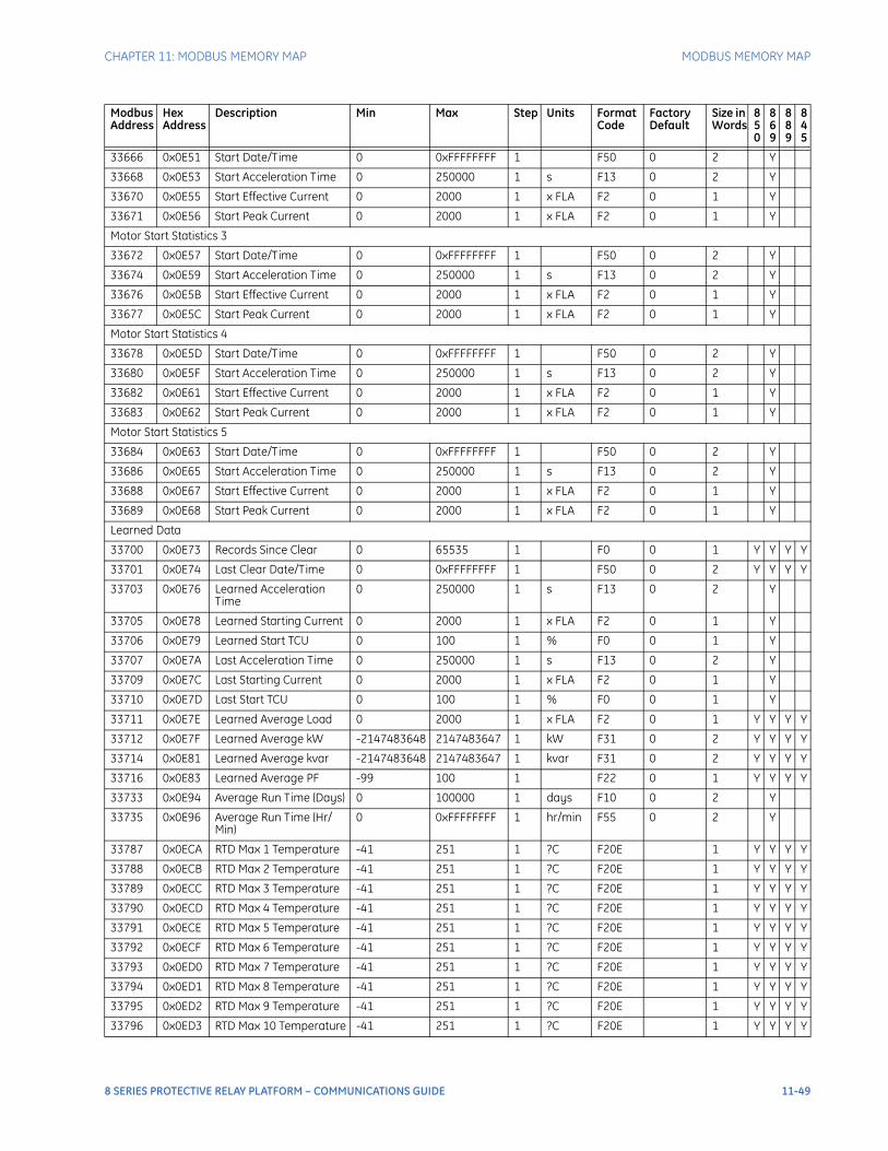
CHAPTER 11: MODBUS MEMORY MAP MODBUS MEMORY MAP
33666 0x0E51 Start Date/Time 0 0xFFFFFFFF 1 F50 0 2 Y
33668 0x0E53 Start Acceleration Time 0 250000 1 s F13 0 2 Y
33670 0x0E55 Start Effective Current 0 2000 1 x FLA F2 0 1 Y
33671 0x0E56 Start Peak Current 0 2000 1 x FLA F2 0 1 Y
Motor Start Statistics 3
33672 0x0E57 Start Date/Time 0 0xFFFFFFFF 1 F50 0 2 Y
33674 0x0E59 Start Acceleration Time 0 250000 1 s F13 0 2 Y
33676 0x0E5B Start Effective Current 0 2000 1 x FLA F2 0 1 Y
33677 0x0E5C Start Peak Current 0 2000 1 x FLA F2 0 1 Y
Motor Start Statistics 4
33678 0x0E5D Start Date/Time 0 0xFFFFFFFF 1 F50 0 2 Y
33680 0x0E5F Start Acceleration Time 0 250000 1 s F13 0 2 Y
33682 0x0E61 Start Effective Current 0 2000 1 x FLA F2 0 1 Y
33683 0x0E62 Start Peak Current 0 2000 1 x FLA F2 0 1 Y
Motor Start Statistics 5
33684 0x0E63 Start Date/Time 0 0xFFFFFFFF 1 F50 0 2 Y
33686 0x0E65 Start Acceleration Time 0 250000 1 s F13 0 2 Y
33688 0x0E67 Start Effective Current 0 2000 1 x FLA F2 0 1 Y
33689 0x0E68 Start Peak Current 0 2000 1 x FLA F2 0 1 Y
Learned Data
33700 0x0E73 Records Since Clear 0 65535 1 F0 0 1 Y Y Y Y
33701 0x0E74 Last Clear Date/Time 0 0xFFFFFFFF 1 F50 0 2 Y Y Y Y
33703 0x0E76 Learned Acceleration Time
0 250000 1 s F13 0 2 Y
33705 0x0E78 Learned Starting Current 0 2000 1 x FLA F2 0 1 Y
33706 0x0E79 Learned Start TCU 0 100 1 % F0 0 1 Y
33707 0x0E7A Last Acceleration Time 0 250000 1 s F13 0 2 Y
33709 0x0E7C Last Starting Current 0 2000 1 x FLA F2 0 1 Y
33710 0x0E7D Last Start TCU 0 100 1 % F0 0 1 Y
33711 0x0E7E Learned Average Load 0 2000 1 x FLA F2 0 1 Y Y Y Y
33712 0x0E7F Learned Average kW -2147483648 2147483647 1 kW F31 0 2 Y Y Y Y
33714 0x0E81 Learned Average kvar -2147483648 2147483647 1 kvar F31 0 2 Y Y Y Y
33716 0x0E83 Learned Average PF -99 100 1 F22 0 1 Y Y Y Y
33733 0x0E94 Average Run Time (Days) 0 100000 1 days F10 0 2 Y
33735 0x0E96 Average Run Time (Hr/Min)
0 0xFFFFFFFF 1 hr/min F55 0 2 Y
33787 0x0ECA RTD Max 1 Temperature -41 251 1 ?C F20E 1 Y Y Y Y
33788 0x0ECB RTD Max 2 Temperature -41 251 1 ?C F20E 1 Y Y Y Y
33789 0x0ECC RTD Max 3 Temperature -41 251 1 ?C F20E 1 Y Y Y Y
33790 0x0ECD RTD Max 4 Temperature -41 251 1 ?C F20E 1 Y Y Y Y
33791 0x0ECE RTD Max 5 Temperature -41 251 1 ?C F20E 1 Y Y Y Y
33792 0x0ECF RTD Max 6 Temperature -41 251 1 ?C F20E 1 Y Y Y Y
33793 0x0ED0 RTD Max 7 Temperature -41 251 1 ?C F20E 1 Y Y Y Y
33794 0x0ED1 RTD Max 8 Temperature -41 251 1 ?C F20E 1 Y Y Y Y
33795 0x0ED2 RTD Max 9 Temperature -41 251 1 ?C F20E 1 Y Y Y Y
33796 0x0ED3 RTD Max 10 Temperature -41 251 1 ?C F20E 1 Y Y Y Y
Modbus Address
Hex Address
Description Min Max Step Units Format Code
Factory Default
Size in Words
850
869
889
845
8 SERIES PROTECTIVE RELAY PLATFORM – COMMUNICATIONS GUIDE 11-49
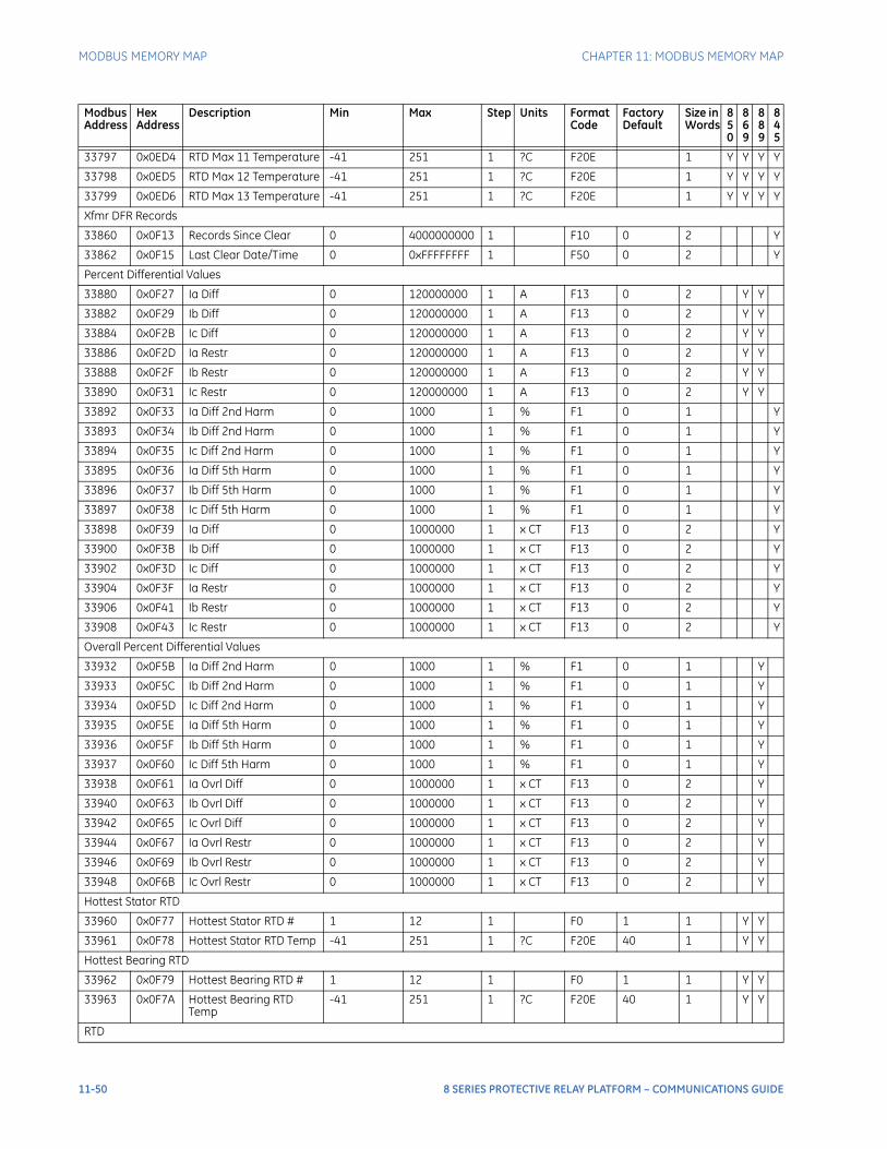
MODBUS MEMORY MAP CHAPTER 11: MODBUS MEMORY MAP
33797 0x0ED4 RTD Max 11 Temperature -41 251 1 ?C F20E 1 Y Y Y Y
33798 0x0ED5 RTD Max 12 Temperature -41 251 1 ?C F20E 1 Y Y Y Y
33799 0x0ED6 RTD Max 13 Temperature -41 251 1 ?C F20E 1 Y Y Y Y
Xfmr DFR Records
33860 0x0F13 Records Since Clear 0 4000000000 1 F10 0 2 Y
33862 0x0F15 Last Clear Date/Time 0 0xFFFFFFFF 1 F50 0 2 Y
Percent Differential Values
33880 0x0F27 Ia Diff 0 120000000 1 A F13 0 2 Y Y
33882 0x0F29 Ib Diff 0 120000000 1 A F13 0 2 Y Y
33884 0x0F2B Ic Diff 0 120000000 1 A F13 0 2 Y Y
33886 0x0F2D Ia Restr 0 120000000 1 A F13 0 2 Y Y
33888 0x0F2F Ib Restr 0 120000000 1 A F13 0 2 Y Y
33890 0x0F31 Ic Restr 0 120000000 1 A F13 0 2 Y Y
33892 0x0F33 Ia Diff 2nd Harm 0 1000 1 % F1 0 1 Y
33893 0x0F34 Ib Diff 2nd Harm 0 1000 1 % F1 0 1 Y
33894 0x0F35 Ic Diff 2nd Harm 0 1000 1 % F1 0 1 Y
33895 0x0F36 Ia Diff 5th Harm 0 1000 1 % F1 0 1 Y
33896 0x0F37 Ib Diff 5th Harm 0 1000 1 % F1 0 1 Y
33897 0x0F38 Ic Diff 5th Harm 0 1000 1 % F1 0 1 Y
33898 0x0F39 Ia Diff 0 1000000 1 x CT F13 0 2 Y
33900 0x0F3B Ib Diff 0 1000000 1 x CT F13 0 2 Y
33902 0x0F3D Ic Diff 0 1000000 1 x CT F13 0 2 Y
33904 0x0F3F Ia Restr 0 1000000 1 x CT F13 0 2 Y
33906 0x0F41 Ib Restr 0 1000000 1 x CT F13 0 2 Y
33908 0x0F43 Ic Restr 0 1000000 1 x CT F13 0 2 Y
Overall Percent Differential Values
33932 0x0F5B Ia Diff 2nd Harm 0 1000 1 % F1 0 1 Y
33933 0x0F5C Ib Diff 2nd Harm 0 1000 1 % F1 0 1 Y
33934 0x0F5D Ic Diff 2nd Harm 0 1000 1 % F1 0 1 Y
33935 0x0F5E Ia Diff 5th Harm 0 1000 1 % F1 0 1 Y
33936 0x0F5F Ib Diff 5th Harm 0 1000 1 % F1 0 1 Y
33937 0x0F60 Ic Diff 5th Harm 0 1000 1 % F1 0 1 Y
33938 0x0F61 Ia Ovrl Diff 0 1000000 1 x CT F13 0 2 Y
33940 0x0F63 Ib Ovrl Diff 0 1000000 1 x CT F13 0 2 Y
33942 0x0F65 Ic Ovrl Diff 0 1000000 1 x CT F13 0 2 Y
33944 0x0F67 Ia Ovrl Restr 0 1000000 1 x CT F13 0 2 Y
33946 0x0F69 Ib Ovrl Restr 0 1000000 1 x CT F13 0 2 Y
33948 0x0F6B Ic Ovrl Restr 0 1000000 1 x CT F13 0 2 Y
Hottest Stator RTD
33960 0x0F77 Hottest Stator RTD # 1 12 1 F0 1 1 Y Y
33961 0x0F78 Hottest Stator RTD Temp -41 251 1 ?C F20E 40 1 Y Y
Hottest Bearing RTD
33962 0x0F79 Hottest Bearing RTD # 1 12 1 F0 1 1 Y Y
33963 0x0F7A Hottest Bearing RTD Temp
-41 251 1 ?C F20E 40 1 Y Y
RTD
Modbus Address
Hex Address
Description Min Max Step Units Format Code
Factory Default
Size in Words
850
869
889
845
11-50 8 SERIES PROTECTIVE RELAY PLATFORM – COMMUNICATIONS GUIDE

CHAPTER 11: MODBUS MEMORY MAP MODBUS MEMORY MAP
33980 0x0F8B RTD 1 -41 251 1 ?C F20E 40 1 Y Y Y Y
33981 0x0F8C RTD 2 -41 251 1 ?C F20E 40 1 Y Y Y Y
33982 0x0F8D RTD 3 -41 251 1 ?C F20E 40 1 Y Y Y Y
33983 0x0F8E RTD 4 -41 251 1 ?C F20E 40 1 Y Y Y Y
33984 0x0F8F RTD 5 -41 251 1 ?C F20E 40 1 Y Y Y Y
33985 0x0F90 RTD 6 -41 251 1 ?C F20E 40 1 Y Y Y Y
33986 0x0F91 RTD 7 -41 251 1 ?C F20E 40 1 Y Y Y Y
33987 0x0F92 RTD 8 -41 251 1 ?C F20E 40 1 Y Y Y Y
33988 0x0F93 RTD 9 -41 251 1 ?C F20E 40 1 Y Y Y Y
33989 0x0F94 RTD 10 -41 251 1 ?C F20E 40 1 Y Y Y Y
33990 0x0F95 RTD 11 -41 251 1 ?C F20E 40 1 Y Y Y Y
33991 0x0F96 RTD 12 -41 251 1 ?C F20E 40 1 Y Y Y Y
33992 0x0F97 RTD 13 -41 251 1 ?C F20E 40 1 Y Y Y Y
RTD Maximums Last Reset
34000 0x0F9F Reset RTD Date/Time 0 0xFFFFFFFF 1 F50 0 2 Y Y Y Y
RTD 1 Maximums
34010 0x0FA9 RTD 1 Max -41 251 1 ?C F20E 40 1 Y Y Y Y
34011 0x0FAA RTD 1 Max Date/Time 0 0xFFFFFFFF 1 F50 0 2 Y Y Y Y
RTD 2 Maximums
34013 0x0FAC RTD 2 Max -41 251 1 ?C F20E 40 1 Y Y Y Y
34014 0x0FAD RTD 2 Max Date/Time 0 0xFFFFFFFF 1 F50 0 2 Y Y Y Y
RTD 3 Maximums
34016 0x0FAF RTD 3 Max -41 251 1 ?C F20E 40 1 Y Y Y Y
34017 0x0FB0 RTD 3 Max Date/Time 0 0xFFFFFFFF 1 F50 0 2 Y Y Y Y
RTD 4 Maximums
34019 0x0FB2 RTD 4 Max -41 251 1 ?C F20E 40 1 Y Y Y Y
34020 0x0FB3 RTD 4 Max Date/Time 0 0xFFFFFFFF 1 F50 0 2 Y Y Y Y
RTD 5 Maximums
34022 0x0FB5 RTD 5 Max -41 251 1 ?C F20E 40 1 Y Y Y Y
34023 0x0FB6 RTD 5 Max Date/Time 0 0xFFFFFFFF 1 F50 0 2 Y Y Y Y
RTD 6 Maximums
34025 0x0FB8 RTD 6 Max -41 251 1 ?C F20E 40 1 Y Y Y Y
34026 0x0FB9 RTD 6 Max Date/Time 0 0xFFFFFFFF 1 F50 0 2 Y Y Y Y
RTD 7 Maximums
34028 0x0FBB RTD 7 Max -41 251 1 ?C F20E 40 1 Y Y Y Y
34029 0x0FBC RTD 7 Max Date/Time 0 0xFFFFFFFF 1 F50 0 2 Y Y Y Y
RTD 8 Maximums
34031 0x0FBE RTD 8 Max -41 251 1 ?C F20E 40 1 Y Y Y Y
34032 0x0FBF RTD 8 Max Date/Time 0 0xFFFFFFFF 1 F50 0 2 Y Y Y Y
RTD 9 Maximums
34034 0x0FC1 RTD 9 Max -41 251 1 ?C F20E 40 1 Y Y Y Y
34035 0x0FC2 RTD 9 Max Date/Time 0 0xFFFFFFFF 1 F50 0 2 Y Y Y Y
RTD 10 Maximums
34037 0x0FC4 RTD 10 Max -41 251 1 ?C F20E 40 1 Y Y Y Y
34038 0x0FC5 RTD 10 Max Date/Time 0 0xFFFFFFFF 1 F50 0 2 Y Y Y Y
Modbus Address
Hex Address
Description Min Max Step Units Format Code
Factory Default
Size in Words
850
869
889
845
8 SERIES PROTECTIVE RELAY PLATFORM – COMMUNICATIONS GUIDE 11-51
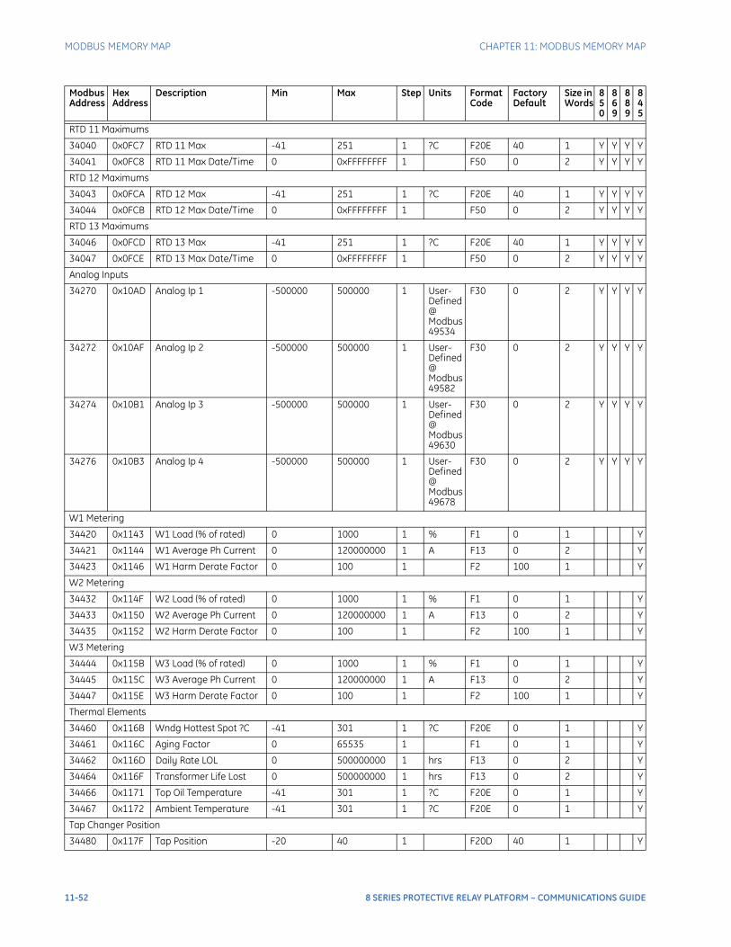
MODBUS MEMORY MAP CHAPTER 11: MODBUS MEMORY MAP
RTD 11 Maximums
34040 0x0FC7 RTD 11 Max -41 251 1 ?C F20E 40 1 Y Y Y Y
34041 0x0FC8 RTD 11 Max Date/Time 0 0xFFFFFFFF 1 F50 0 2 Y Y Y Y
RTD 12 Maximums
34043 0x0FCA RTD 12 Max -41 251 1 ?C F20E 40 1 Y Y Y Y
34044 0x0FCB RTD 12 Max Date/Time 0 0xFFFFFFFF 1 F50 0 2 Y Y Y Y
RTD 13 Maximums
34046 0x0FCD RTD 13 Max -41 251 1 ?C F20E 40 1 Y Y Y Y
34047 0x0FCE RTD 13 Max Date/Time 0 0xFFFFFFFF 1 F50 0 2 Y Y Y Y
Analog Inputs
34270 0x10AD Analog Ip 1 -500000 500000 1 User-Defined @ Modbus 49534
F30 0 2 Y Y Y Y
34272 0x10AF Analog Ip 2 -500000 500000 1 User-Defined @ Modbus 49582
F30 0 2 Y Y Y Y
34274 0x10B1 Analog Ip 3 -500000 500000 1 User-Defined @ Modbus 49630
F30 0 2 Y Y Y Y
34276 0x10B3 Analog Ip 4 -500000 500000 1 User-Defined @ Modbus 49678
F30 0 2 Y Y Y Y
W1 Metering
34420 0x1143 W1 Load (% of rated) 0 1000 1 % F1 0 1 Y
34421 0x1144 W1 Average Ph Current 0 120000000 1 A F13 0 2 Y
34423 0x1146 W1 Harm Derate Factor 0 100 1 F2 100 1 Y
W2 Metering
34432 0x114F W2 Load (% of rated) 0 1000 1 % F1 0 1 Y
34433 0x1150 W2 Average Ph Current 0 120000000 1 A F13 0 2 Y
34435 0x1152 W2 Harm Derate Factor 0 100 1 F2 100 1 Y
W3 Metering
34444 0x115B W3 Load (% of rated) 0 1000 1 % F1 0 1 Y
34445 0x115C W3 Average Ph Current 0 120000000 1 A F13 0 2 Y
34447 0x115E W3 Harm Derate Factor 0 100 1 F2 100 1 Y
Thermal Elements
34460 0x116B Wndg Hottest Spot ?C -41 301 1 ?C F20E 0 1 Y
34461 0x116C Aging Factor 0 65535 1 F1 0 1 Y
34462 0x116D Daily Rate LOL 0 500000000 1 hrs F13 0 2 Y
34464 0x116F Transformer Life Lost 0 500000000 1 hrs F13 0 2 Y
34466 0x1171 Top Oil Temperature -41 301 1 ?C F20E 0 1 Y
34467 0x1172 Ambient Temperature -41 301 1 ?C F20E 0 1 Y
Tap Changer Position
34480 0x117F Tap Position -20 40 1 F20D 40 1 Y
Modbus Address
Hex Address
Description Min Max Step Units Format Code
Factory Default
Size in Words
850
869
889
845
11-52 8 SERIES PROTECTIVE RELAY PLATFORM – COMMUNICATIONS GUIDE
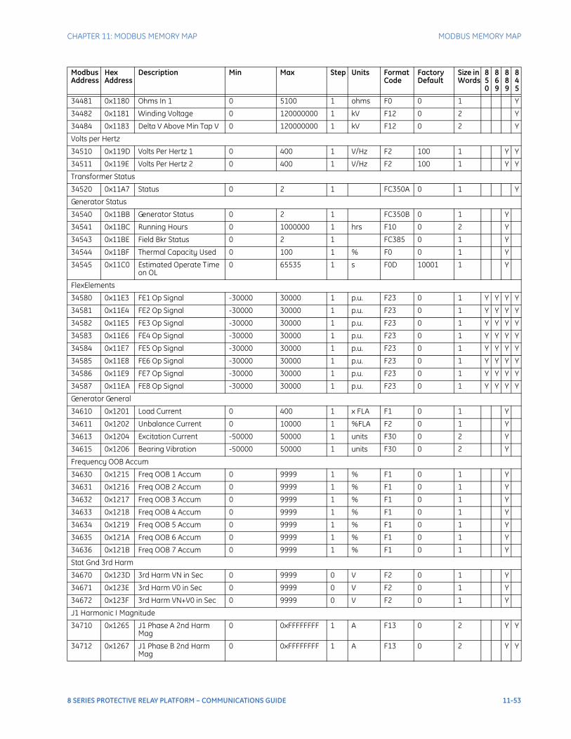
CHAPTER 11: MODBUS MEMORY MAP MODBUS MEMORY MAP
34481 0x1180 Ohms In 1 0 5100 1 ohms F0 0 1 Y
34482 0x1181 Winding Voltage 0 120000000 1 kV F12 0 2 Y
34484 0x1183 Delta V Above Min Tap V 0 120000000 1 kV F12 0 2 Y
Volts per Hertz
34510 0x119D Volts Per Hertz 1 0 400 1 V/Hz F2 100 1 Y Y
34511 0x119E Volts Per Hertz 2 0 400 1 V/Hz F2 100 1 Y Y
Transformer Status
34520 0x11A7 Status 0 2 1 FC350A 0 1 Y
Generator Status
34540 0x11BB Generator Status 0 2 1 FC350B 0 1 Y
34541 0x11BC Running Hours 0 1000000 1 hrs F10 0 2 Y
34543 0x11BE Field Bkr Status 0 2 1 FC385 0 1 Y
34544 0x11BF Thermal Capacity Used 0 100 1 % F0 0 1 Y
34545 0x11C0 Estimated Operate Time on OL
0 65535 1 s F0D 10001 1 Y
FlexElements
34580 0x11E3 FE1 Op Signal -30000 30000 1 p.u. F23 0 1 Y Y Y Y
34581 0x11E4 FE2 Op Signal -30000 30000 1 p.u. F23 0 1 Y Y Y Y
34582 0x11E5 FE3 Op Signal -30000 30000 1 p.u. F23 0 1 Y Y Y Y
34583 0x11E6 FE4 Op Signal -30000 30000 1 p.u. F23 0 1 Y Y Y Y
34584 0x11E7 FE5 Op Signal -30000 30000 1 p.u. F23 0 1 Y Y Y Y
34585 0x11E8 FE6 Op Signal -30000 30000 1 p.u. F23 0 1 Y Y Y Y
34586 0x11E9 FE7 Op Signal -30000 30000 1 p.u. F23 0 1 Y Y Y Y
34587 0x11EA FE8 Op Signal -30000 30000 1 p.u. F23 0 1 Y Y Y Y
Generator General
34610 0x1201 Load Current 0 400 1 x FLA F1 0 1 Y
34611 0x1202 Unbalance Current 0 10000 1 %FLA F2 0 1 Y
34613 0x1204 Excitation Current -50000 50000 1 units F30 0 2 Y
34615 0x1206 Bearing Vibration -50000 50000 1 units F30 0 2 Y
Frequency OOB Accum
34630 0x1215 Freq OOB 1 Accum 0 9999 1 % F1 0 1 Y
34631 0x1216 Freq OOB 2 Accum 0 9999 1 % F1 0 1 Y
34632 0x1217 Freq OOB 3 Accum 0 9999 1 % F1 0 1 Y
34633 0x1218 Freq OOB 4 Accum 0 9999 1 % F1 0 1 Y
34634 0x1219 Freq OOB 5 Accum 0 9999 1 % F1 0 1 Y
34635 0x121A Freq OOB 6 Accum 0 9999 1 % F1 0 1 Y
34636 0x121B Freq OOB 7 Accum 0 9999 1 % F1 0 1 Y
Stat Gnd 3rd Harm
34670 0x123D 3rd Harm VN in Sec 0 9999 0 V F2 0 1 Y
34671 0x123E 3rd Harm V0 in Sec 0 9999 0 V F2 0 1 Y
34672 0x123F 3rd Harm VN+V0 in Sec 0 9999 0 V F2 0 1 Y
J1 Harmonic I Magnitude
34710 0x1265 J1 Phase A 2nd Harm Mag
0 0xFFFFFFFF 1 A F13 0 2 Y Y
34712 0x1267 J1 Phase B 2nd Harm Mag
0 0xFFFFFFFF 1 A F13 0 2 Y Y
Modbus Address
Hex Address
Description Min Max Step Units Format Code
Factory Default
Size in Words
850
869
889
845
8 SERIES PROTECTIVE RELAY PLATFORM – COMMUNICATIONS GUIDE 11-53
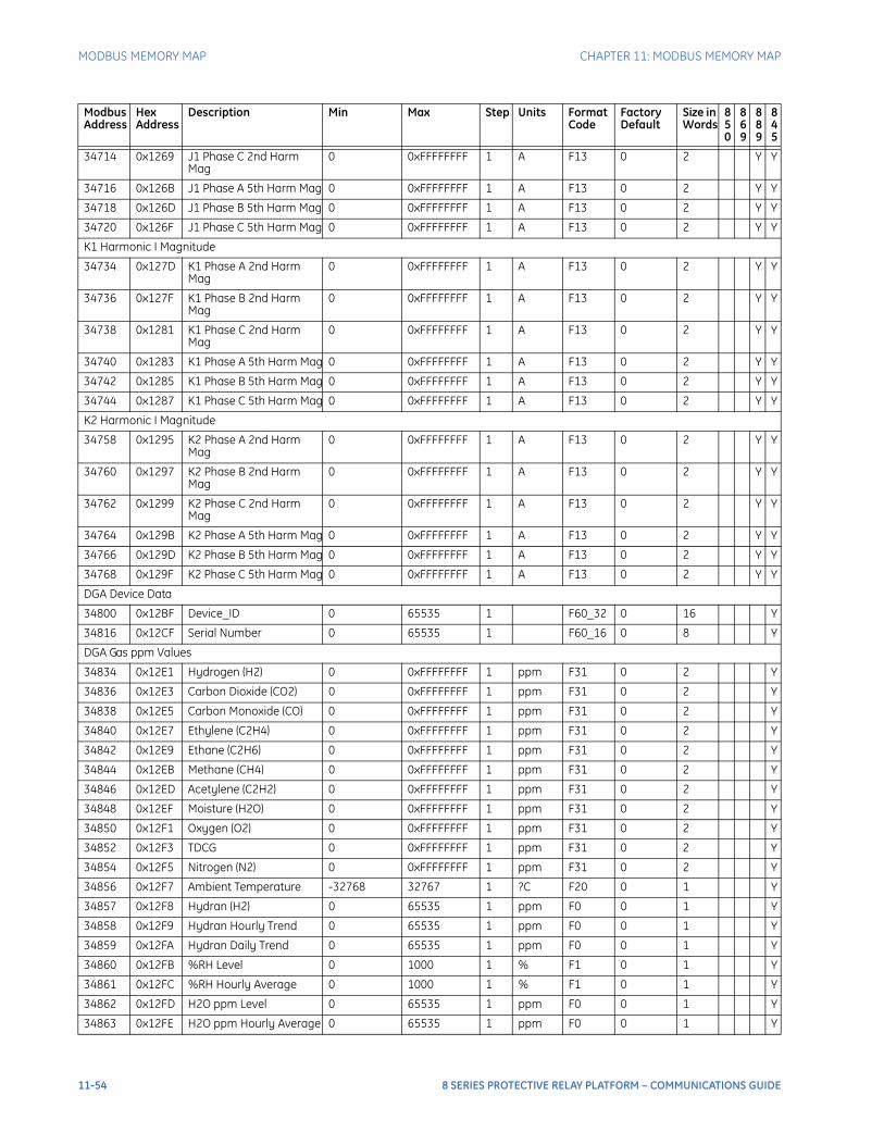
MODBUS MEMORY MAP CHAPTER 11: MODBUS MEMORY MAP
34714 0x1269 J1 Phase C 2nd Harm Mag
0 0xFFFFFFFF 1 A F13 0 2 Y Y
34716 0x126B J1 Phase A 5th Harm Mag 0 0xFFFFFFFF 1 A F13 0 2 Y Y
34718 0x126D J1 Phase B 5th Harm Mag 0 0xFFFFFFFF 1 A F13 0 2 Y Y
34720 0x126F J1 Phase C 5th Harm Mag 0 0xFFFFFFFF 1 A F13 0 2 Y Y
K1 Harmonic I Magnitude
34734 0x127D K1 Phase A 2nd Harm Mag
0 0xFFFFFFFF 1 A F13 0 2 Y Y
34736 0x127F K1 Phase B 2nd Harm Mag
0 0xFFFFFFFF 1 A F13 0 2 Y Y
34738 0x1281 K1 Phase C 2nd Harm Mag
0 0xFFFFFFFF 1 A F13 0 2 Y Y
34740 0x1283 K1 Phase A 5th Harm Mag 0 0xFFFFFFFF 1 A F13 0 2 Y Y
34742 0x1285 K1 Phase B 5th Harm Mag 0 0xFFFFFFFF 1 A F13 0 2 Y Y
34744 0x1287 K1 Phase C 5th Harm Mag 0 0xFFFFFFFF 1 A F13 0 2 Y Y
K2 Harmonic I Magnitude
34758 0x1295 K2 Phase A 2nd Harm Mag
0 0xFFFFFFFF 1 A F13 0 2 Y Y
34760 0x1297 K2 Phase B 2nd Harm Mag
0 0xFFFFFFFF 1 A F13 0 2 Y Y
34762 0x1299 K2 Phase C 2nd Harm Mag
0 0xFFFFFFFF 1 A F13 0 2 Y Y
34764 0x129B K2 Phase A 5th Harm Mag 0 0xFFFFFFFF 1 A F13 0 2 Y Y
34766 0x129D K2 Phase B 5th Harm Mag 0 0xFFFFFFFF 1 A F13 0 2 Y Y
34768 0x129F K2 Phase C 5th Harm Mag 0 0xFFFFFFFF 1 A F13 0 2 Y Y
DGA Device Data
34800 0x12BF Device_ID 0 65535 1 F60_32 0 16 Y
34816 0x12CF Serial Number 0 65535 1 F60_16 0 8 Y
DGA Gas ppm Values
34834 0x12E1 Hydrogen (H2) 0 0xFFFFFFFF 1 ppm F31 0 2 Y
34836 0x12E3 Carbon Dioxide (CO2) 0 0xFFFFFFFF 1 ppm F31 0 2 Y
34838 0x12E5 Carbon Monoxide (CO) 0 0xFFFFFFFF 1 ppm F31 0 2 Y
34840 0x12E7 Ethylene (C2H4) 0 0xFFFFFFFF 1 ppm F31 0 2 Y
34842 0x12E9 Ethane (C2H6) 0 0xFFFFFFFF 1 ppm F31 0 2 Y
34844 0x12EB Methane (CH4) 0 0xFFFFFFFF 1 ppm F31 0 2 Y
34846 0x12ED Acetylene (C2H2) 0 0xFFFFFFFF 1 ppm F31 0 2 Y
34848 0x12EF Moisture (H2O) 0 0xFFFFFFFF 1 ppm F31 0 2 Y
34850 0x12F1 Oxygen (O2) 0 0xFFFFFFFF 1 ppm F31 0 2 Y
34852 0x12F3 TDCG 0 0xFFFFFFFF 1 ppm F31 0 2 Y
34854 0x12F5 Nitrogen (N2) 0 0xFFFFFFFF 1 ppm F31 0 2 Y
34856 0x12F7 Ambient Temperature -32768 32767 1 ?C F20 0 1 Y
34857 0x12F8 Hydran (H2) 0 65535 1 ppm F0 0 1 Y
34858 0x12F9 Hydran Hourly Trend 0 65535 1 ppm F0 0 1 Y
34859 0x12FA Hydran Daily Trend 0 65535 1 ppm F0 0 1 Y
34860 0x12FB %RH Level 0 1000 1 % F1 0 1 Y
34861 0x12FC %RH Hourly Average 0 1000 1 % F1 0 1 Y
34862 0x12FD H2O ppm Level 0 65535 1 ppm F0 0 1 Y
34863 0x12FE H2O ppm Hourly Average 0 65535 1 ppm F0 0 1 Y
Modbus Address
Hex Address
Description Min Max Step Units Format Code
Factory Default
Size in Words
850
869
889
845
11-54 8 SERIES PROTECTIVE RELAY PLATFORM – COMMUNICATIONS GUIDE
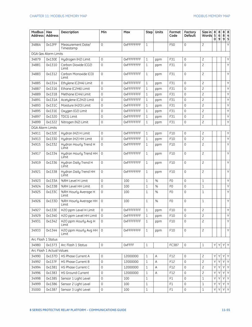
CHAPTER 11: MODBUS MEMORY MAP MODBUS MEMORY MAP
34864 0x12FF Measurement Date/Timestamp
0 0xFFFFFFFF 1 F50 0 2 Y
DGA Gas Alarm Limits
34879 0x130E Hydrogen (H2) Limit 0 0xFFFFFFFF 1 ppm F31 0 2 Y
34881 0x1310 Carbon Dioxide (CO2) Limit
0 0xFFFFFFFF 1 ppm F31 0 2 Y
34883 0x1312 Carbon Monoxide (CO) Limit
0 0xFFFFFFFF 1 ppm F31 0 2 Y
34885 0x1314 Ethylene (C2H4) Limit 0 0xFFFFFFFF 1 ppm F31 0 2 Y
34887 0x1316 Ethane (C2H6) Limit 0 0xFFFFFFFF 1 ppm F31 0 2 Y
34889 0x1318 Methane (CH4) Limit 0 0xFFFFFFFF 1 ppm F31 0 2 Y
34891 0x131A Acetylene (C2H2) Limit 0 0xFFFFFFFF 1 ppm F31 0 2 Y
34893 0x131C Moisture (H2O) Limit 0 0xFFFFFFFF 1 ppm F31 0 2 Y
34895 0x131E Oxygen (O2) Limit 0 0xFFFFFFFF 1 ppm F31 0 2 Y
34897 0x1320 TDCG Limit 0 0xFFFFFFFF 1 ppm F31 0 2 Y
34899 0x1322 Nitrogen (N2) Limit 0 0xFFFFFFFF 1 ppm F31 0 2 Y
DGA Alarm Limits
34911 0x132E Hydran (H2) H Limit 0 0xFFFFFFFF 1 ppm F10 0 2 Y
34913 0x1330 Hydran (H2) HH Limit 0 0xFFFFFFFF 1 ppm F10 0 2 Y
34915 0x1332 Hydran Hourly Trend H Limit
0 0xFFFFFFFF 1 ppm F10 0 2 Y
34917 0x1334 Hydran Hourly Trend HH Limit
0 0xFFFFFFFF 1 ppm F10 0 2 Y
34919 0x1336 Hydran Daily Trend H Limit
0 0xFFFFFFFF 1 ppm F10 0 2 Y
34921 0x1338 Hydran Daily Trend HH Limit
0 0xFFFFFFFF 1 ppm F10 0 2 Y
34923 0x133A %RH Level H Limit 0 100 1 % F0 0 1 Y
34924 0x133B %RH Level HH Limit 0 100 1 % F0 0 1 Y
34925 0x133C %RH Hourly Average H Limit
0 100 1 % F0 0 1 Y
34926 0x133D %RH Hourly Average HH Limit
0 100 1 % F0 0 1 Y
34927 0x133E H2O ppm Level H Limit 0 0xFFFFFFFF 1 ppm F10 0 2 Y
34929 0x1340 H2O ppm Level HH Limit 0 0xFFFFFFFF 1 ppm F10 0 2 Y
34931 0x1342 H2O ppm Hourly Avg H Limit
0 0xFFFFFFFF 1 ppm F10 0 2 Y
34933 0x1344 H2O ppm Hourly Avg HH Limit
0 0xFFFFFFFF 1 ppm F10 0 2 Y
Arc Flash 1 Status
34980 0x1373 Arc Flash 1 Status 0 0xFFFF 1 FC387 0 1 Y Y Y Y
Arc Flash 1 Actual Values
34990 0x137D HS Phase Current A 0 12000000 1 A F12 0 2 Y Y Y Y
34992 0x137F HS Phase Current B 0 12000000 1 A F12 0 2 Y Y Y Y
34994 0x1381 HS Phase Current C 0 12000000 1 A F12 0 2 Y Y Y Y
34996 0x1383 HS Ground Current 0 12000000 1 A F12 0 2 Y Y Y Y
34998 0x1385 Sensor 1 Light Level 0 100 1 F1 0 1 Y Y Y Y
34999 0x1386 Sensor 2 Light Level 0 100 1 F1 0 1 Y Y Y Y
35000 0x1387 Sensor 3 Light Level 0 100 1 F1 0 1 Y Y Y Y
Modbus Address
Hex Address
Description Min Max Step Units Format Code
Factory Default
Size in Words
850
869
889
845
8 SERIES PROTECTIVE RELAY PLATFORM – COMMUNICATIONS GUIDE 11-55
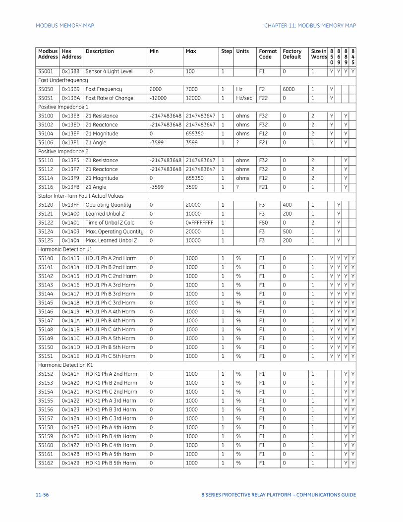
MODBUS MEMORY MAP CHAPTER 11: MODBUS MEMORY MAP
35001 0x1388 Sensor 4 Light Level 0 100 1 F1 0 1 Y Y Y Y
Fast Underfrequency
35050 0x13B9 Fast Frequency 2000 7000 1 Hz F2 6000 1 Y
35051 0x13BA Fast Rate of Change -12000 12000 1 Hz/sec F22 0 1 Y
Positive Impedance 1
35100 0x13EB Z1 Resistance -2147483648 2147483647 1 ohms F32 0 2 Y Y
35102 0x13ED Z1 Reactance -2147483648 2147483647 1 ohms F32 0 2 Y Y
35104 0x13EF Z1 Magnitude 0 655350 1 ohms F12 0 2 Y Y
35106 0x13F1 Z1 Angle -3599 3599 1 ? F21 0 1 Y Y
Positive Impedance 2
35110 0x13F5 Z1 Resistance -2147483648 2147483647 1 ohms F32 0 2 Y
35112 0x13F7 Z1 Reactance -2147483648 2147483647 1 ohms F32 0 2 Y
35114 0x13F9 Z1 Magnitude 0 655350 1 ohms F12 0 2 Y
35116 0x13FB Z1 Angle -3599 3599 1 ? F21 0 1 Y
Stator Inter-Turn Fault Actual Values
35120 0x13FF Operating Quantity 0 20000 1 F3 400 1 Y
35121 0x1400 Learned Unbal Z 0 10000 1 F3 200 1 Y
35122 0x1401 Time of Unbal Z Calc 0 0xFFFFFFFF 1 F50 0 2 Y
35124 0x1403 Max. Operating Quantity 0 20000 1 F3 500 1 Y
35125 0x1404 Max. Learned Unbal Z 0 10000 1 F3 200 1 Y
Harmonic Detection J1
35140 0x1413 HD J1 Ph A 2nd Harm 0 1000 1 % F1 0 1 Y Y Y Y
35141 0x1414 HD J1 Ph B 2nd Harm 0 1000 1 % F1 0 1 Y Y Y Y
35142 0x1415 HD J1 Ph C 2nd Harm 0 1000 1 % F1 0 1 Y Y Y Y
35143 0x1416 HD J1 Ph A 3rd Harm 0 1000 1 % F1 0 1 Y Y Y Y
35144 0x1417 HD J1 Ph B 3rd Harm 0 1000 1 % F1 0 1 Y Y Y Y
35145 0x1418 HD J1 Ph C 3rd Harm 0 1000 1 % F1 0 1 Y Y Y Y
35146 0x1419 HD J1 Ph A 4th Harm 0 1000 1 % F1 0 1 Y Y Y Y
35147 0x141A HD J1 Ph B 4th Harm 0 1000 1 % F1 0 1 Y Y Y Y
35148 0x141B HD J1 Ph C 4th Harm 0 1000 1 % F1 0 1 Y Y Y Y
35149 0x141C HD J1 Ph A 5th Harm 0 1000 1 % F1 0 1 Y Y Y Y
35150 0x141D HD J1 Ph B 5th Harm 0 1000 1 % F1 0 1 Y Y Y Y
35151 0x141E HD J1 Ph C 5th Harm 0 1000 1 % F1 0 1 Y Y Y Y
Harmonic Detection K1
35152 0x141F HD K1 Ph A 2nd Harm 0 1000 1 % F1 0 1 Y Y
35153 0x1420 HD K1 Ph B 2nd Harm 0 1000 1 % F1 0 1 Y Y
35154 0x1421 HD K1 Ph C 2nd Harm 0 1000 1 % F1 0 1 Y Y
35155 0x1422 HD K1 Ph A 3rd Harm 0 1000 1 % F1 0 1 Y Y
35156 0x1423 HD K1 Ph B 3rd Harm 0 1000 1 % F1 0 1 Y Y
35157 0x1424 HD K1 Ph C 3rd Harm 0 1000 1 % F1 0 1 Y Y
35158 0x1425 HD K1 Ph A 4th Harm 0 1000 1 % F1 0 1 Y Y
35159 0x1426 HD K1 Ph B 4th Harm 0 1000 1 % F1 0 1 Y Y
35160 0x1427 HD K1 Ph C 4th Harm 0 1000 1 % F1 0 1 Y Y
35161 0x1428 HD K1 Ph A 5th Harm 0 1000 1 % F1 0 1 Y Y
35162 0x1429 HD K1 Ph B 5th Harm 0 1000 1 % F1 0 1 Y Y
Modbus Address
Hex Address
Description Min Max Step Units Format Code
Factory Default
Size in Words
850
869
889
845
11-56 8 SERIES PROTECTIVE RELAY PLATFORM – COMMUNICATIONS GUIDE

CHAPTER 11: MODBUS MEMORY MAP MODBUS MEMORY MAP
35163 0x142A HD K1 Ph C 5th Harm 0 1000 1 % F1 0 1 Y Y
Harmonic Detection K2
35164 0x142B HD K2 Ph A 2nd Harm 0 1000 1 % F1 0 1 Y Y
35165 0x142C HD K2 Ph B 2nd Harm 0 1000 1 % F1 0 1 Y Y
35166 0x142D HD K2 Ph C 2nd Harm 0 1000 1 % F1 0 1 Y Y
35167 0x142E HD K2 Ph A 3rd Harm 0 1000 1 % F1 0 1 Y Y
35168 0x142F HD K2 Ph B 3rd Harm 0 1000 1 % F1 0 1 Y Y
35169 0x1430 HD K2 Ph C 3rd Harm 0 1000 1 % F1 0 1 Y Y
35170 0x1431 HD K2 Ph A 4th Harm 0 1000 1 % F1 0 1 Y Y
35171 0x1432 HD K2 Ph B 4th Harm 0 1000 1 % F1 0 1 Y Y
35172 0x1433 HD K2 Ph C 4th Harm 0 1000 1 % F1 0 1 Y Y
35173 0x1434 HD K2 Ph A 5th Harm 0 1000 1 % F1 0 1 Y Y
35174 0x1435 HD K2 Ph B 5th Harm 0 1000 1 % F1 0 1 Y Y
35175 0x1436 HD K2 Ph C 5th Harm 0 1000 1 % F1 0 1 Y Y
Last Trip Data
35190 0x1445 Cause 0 0xFFFFFFFF 1 FC134 0 2 Y Y Y Y
35192 0x1447 Event 0 4294967295 1 F10 0 2 Y Y Y Y
35194 0x1449 Date/Time 0 0xFFFFFFFF 1 F50 0 2 Y Y Y Y
35196 0x144B Time (us) 0 999999 1 us F51 0 2 Y Y Y Y
35198 0x144D Parameter 1 -2147483648 2147483647 1 F30 0 2 Y Y Y Y
35200 0x144F Parameter 2 -2147483648 2147483647 1 F30 0 2 Y Y Y Y
35202 0x1451 Parameter 3 -2147483648 2147483647 1 F30 0 2 Y Y Y Y
35204 0x1453 Parameter 4 -2147483648 2147483647 1 F30 0 2 Y Y Y Y
35206 0x1455 Parameter 5 -2147483648 2147483647 1 F30 0 2 Y Y Y Y
35208 0x1457 Parameter 6 -2147483648 2147483647 1 F30 0 2 Y Y Y Y
35210 0x1459 Parameter 7 -2147483648 2147483647 1 F30 0 2 Y Y Y Y
35212 0x145B Parameter 8 -2147483648 2147483647 1 F30 0 2 Y Y Y Y
35214 0x145D Parameter 9 -2147483648 2147483647 1 F30 0 2 Y Y Y Y
35216 0x145F Parameter 10 -2147483648 2147483647 1 F30 0 2 Y Y Y Y
35218 0x1461 Parameter 11 -2147483648 2147483647 1 F30 0 2 Y Y Y Y
35220 0x1463 Parameter 12 -2147483648 2147483647 1 F30 0 2 Y Y Y Y
35222 0x1465 Parameter 13 -2147483648 2147483647 1 F30 0 2 Y Y Y Y
35224 0x1467 Parameter 14 -2147483648 2147483647 1 F30 0 2 Y Y Y Y
35226 0x1469 Parameter 15 -2147483648 2147483647 1 F30 0 2 Y Y Y Y
35228 0x146B Parameter 16 -2147483648 2147483647 1 F30 0 2 Y Y Y Y
35230 0x146D Parameter 17 -2147483648 2147483647 1 F30 0 2 Y Y Y Y
35232 0x146F Parameter 18 -2147483648 2147483647 1 F30 0 2 Y Y Y Y
35234 0x1471 Parameter 19 -2147483648 2147483647 1 F30 0 2 Y Y Y Y
35236 0x1473 Parameter 20 -2147483648 2147483647 1 F30 0 2 Y Y Y Y
35238 0x1475 Parameter 21 -2147483648 2147483647 1 F30 0 2 Y Y Y Y
35240 0x1477 Parameter 22 -2147483648 2147483647 1 F30 0 2 Y Y Y Y
35242 0x1479 Parameter 23 -2147483648 2147483647 1 F30 0 2 Y Y Y Y
35244 0x147B Parameter 24 -2147483648 2147483647 1 F30 0 2 Y Y Y Y
35246 0x147D Parameter 25 -2147483648 2147483647 1 F30 0 2 Y Y Y Y
35248 0x147F Parameter 26 -2147483648 2147483647 1 F30 0 2 Y Y Y Y
Modbus Address
Hex Address
Description Min Max Step Units Format Code
Factory Default
Size in Words
850
869
889
845
8 SERIES PROTECTIVE RELAY PLATFORM – COMMUNICATIONS GUIDE 11-57
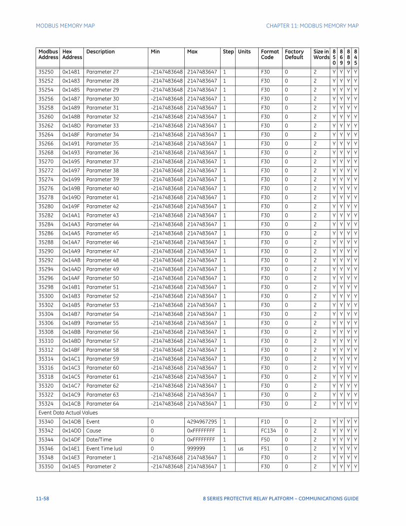
MODBUS MEMORY MAP CHAPTER 11: MODBUS MEMORY MAP
35250 0x1481 Parameter 27 -2147483648 2147483647 1 F30 0 2 Y Y Y Y
35252 0x1483 Parameter 28 -2147483648 2147483647 1 F30 0 2 Y Y Y Y
35254 0x1485 Parameter 29 -2147483648 2147483647 1 F30 0 2 Y Y Y Y
35256 0x1487 Parameter 30 -2147483648 2147483647 1 F30 0 2 Y Y Y Y
35258 0x1489 Parameter 31 -2147483648 2147483647 1 F30 0 2 Y Y Y Y
35260 0x148B Parameter 32 -2147483648 2147483647 1 F30 0 2 Y Y Y Y
35262 0x148D Parameter 33 -2147483648 2147483647 1 F30 0 2 Y Y Y Y
35264 0x148F Parameter 34 -2147483648 2147483647 1 F30 0 2 Y Y Y Y
35266 0x1491 Parameter 35 -2147483648 2147483647 1 F30 0 2 Y Y Y Y
35268 0x1493 Parameter 36 -2147483648 2147483647 1 F30 0 2 Y Y Y Y
35270 0x1495 Parameter 37 -2147483648 2147483647 1 F30 0 2 Y Y Y Y
35272 0x1497 Parameter 38 -2147483648 2147483647 1 F30 0 2 Y Y Y Y
35274 0x1499 Parameter 39 -2147483648 2147483647 1 F30 0 2 Y Y Y Y
35276 0x149B Parameter 40 -2147483648 2147483647 1 F30 0 2 Y Y Y Y
35278 0x149D Parameter 41 -2147483648 2147483647 1 F30 0 2 Y Y Y Y
35280 0x149F Parameter 42 -2147483648 2147483647 1 F30 0 2 Y Y Y Y
35282 0x14A1 Parameter 43 -2147483648 2147483647 1 F30 0 2 Y Y Y Y
35284 0x14A3 Parameter 44 -2147483648 2147483647 1 F30 0 2 Y Y Y Y
35286 0x14A5 Parameter 45 -2147483648 2147483647 1 F30 0 2 Y Y Y Y
35288 0x14A7 Parameter 46 -2147483648 2147483647 1 F30 0 2 Y Y Y Y
35290 0x14A9 Parameter 47 -2147483648 2147483647 1 F30 0 2 Y Y Y Y
35292 0x14AB Parameter 48 -2147483648 2147483647 1 F30 0 2 Y Y Y Y
35294 0x14AD Parameter 49 -2147483648 2147483647 1 F30 0 2 Y Y Y Y
35296 0x14AF Parameter 50 -2147483648 2147483647 1 F30 0 2 Y Y Y Y
35298 0x14B1 Parameter 51 -2147483648 2147483647 1 F30 0 2 Y Y Y Y
35300 0x14B3 Parameter 52 -2147483648 2147483647 1 F30 0 2 Y Y Y Y
35302 0x14B5 Parameter 53 -2147483648 2147483647 1 F30 0 2 Y Y Y Y
35304 0x14B7 Parameter 54 -2147483648 2147483647 1 F30 0 2 Y Y Y Y
35306 0x14B9 Parameter 55 -2147483648 2147483647 1 F30 0 2 Y Y Y Y
35308 0x14BB Parameter 56 -2147483648 2147483647 1 F30 0 2 Y Y Y Y
35310 0x14BD Parameter 57 -2147483648 2147483647 1 F30 0 2 Y Y Y Y
35312 0x14BF Parameter 58 -2147483648 2147483647 1 F30 0 2 Y Y Y Y
35314 0x14C1 Parameter 59 -2147483648 2147483647 1 F30 0 2 Y Y Y Y
35316 0x14C3 Parameter 60 -2147483648 2147483647 1 F30 0 2 Y Y Y Y
35318 0x14C5 Parameter 61 -2147483648 2147483647 1 F30 0 2 Y Y Y Y
35320 0x14C7 Parameter 62 -2147483648 2147483647 1 F30 0 2 Y Y Y Y
35322 0x14C9 Parameter 63 -2147483648 2147483647 1 F30 0 2 Y Y Y Y
35324 0x14CB Parameter 64 -2147483648 2147483647 1 F30 0 2 Y Y Y Y
Event Data Actual Values
35340 0x14DB Event 0 4294967295 1 F10 0 2 Y Y Y Y
35342 0x14DD Cause 0 0xFFFFFFFF 1 FC134 0 2 Y Y Y Y
35344 0x14DF Date/Time 0 0xFFFFFFFF 1 F50 0 2 Y Y Y Y
35346 0x14E1 Event Time (us) 0 999999 1 us F51 0 2 Y Y Y Y
35348 0x14E3 Parameter 1 -2147483648 2147483647 1 F30 0 2 Y Y Y Y
35350 0x14E5 Parameter 2 -2147483648 2147483647 1 F30 0 2 Y Y Y Y
Modbus Address
Hex Address
Description Min Max Step Units Format Code
Factory Default
Size in Words
850
869
889
845
11-58 8 SERIES PROTECTIVE RELAY PLATFORM – COMMUNICATIONS GUIDE
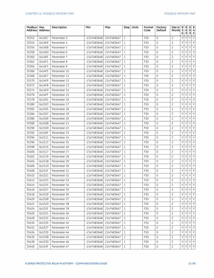
CHAPTER 11: MODBUS MEMORY MAP MODBUS MEMORY MAP
35352 0x14E7 Parameter 3 -2147483648 2147483647 1 F30 0 2 Y Y Y Y
35354 0x14E9 Parameter 4 -2147483648 2147483647 1 F30 0 2 Y Y Y Y
35356 0x14EB Parameter 5 -2147483648 2147483647 1 F30 0 2 Y Y Y Y
35358 0x14ED Parameter 6 -2147483648 2147483647 1 F30 0 2 Y Y Y Y
35360 0x14EF Parameter 7 -2147483648 2147483647 1 F30 0 2 Y Y Y Y
35362 0x14F1 Parameter 8 -2147483648 2147483647 1 F30 0 2 Y Y Y Y
35364 0x14F3 Parameter 9 -2147483648 2147483647 1 F30 0 2 Y Y Y Y
35366 0x14F5 Parameter 10 -2147483648 2147483647 1 F30 0 2 Y Y Y Y
35368 0x14F7 Parameter 11 -2147483648 2147483647 1 F30 0 2 Y Y Y Y
35370 0x14F9 Parameter 12 -2147483648 2147483647 1 F30 0 2 Y Y Y Y
35372 0x14FB Parameter 13 -2147483648 2147483647 1 F30 0 2 Y Y Y Y
35374 0x14FD Parameter 14 -2147483648 2147483647 1 F30 0 2 Y Y Y Y
35376 0x14FF Parameter 15 -2147483648 2147483647 1 F30 0 2 Y Y Y Y
35378 0x1501 Parameter 16 -2147483648 2147483647 1 F30 0 2 Y Y Y Y
35380 0x1503 Parameter 17 -2147483648 2147483647 1 F30 0 2 Y Y Y Y
35382 0x1505 Parameter 18 -2147483648 2147483647 1 F30 0 2 Y Y Y Y
35384 0x1507 Parameter 19 -2147483648 2147483647 1 F30 0 2 Y Y Y Y
35386 0x1509 Parameter 20 -2147483648 2147483647 1 F30 0 2 Y Y Y Y
35388 0x150B Parameter 21 -2147483648 2147483647 1 F30 0 2 Y Y Y Y
35390 0x150D Parameter 22 -2147483648 2147483647 1 F30 0 2 Y Y Y Y
35392 0x150F Parameter 23 -2147483648 2147483647 1 F30 0 2 Y Y Y Y
35394 0x1511 Parameter 24 -2147483648 2147483647 1 F30 0 2 Y Y Y Y
35396 0x1513 Parameter 25 -2147483648 2147483647 1 F30 0 2 Y Y Y Y
35398 0x1515 Parameter 26 -2147483648 2147483647 1 F30 0 2 Y Y Y Y
35400 0x1517 Parameter 27 -2147483648 2147483647 1 F30 0 2 Y Y Y Y
35402 0x1519 Parameter 28 -2147483648 2147483647 1 F30 0 2 Y Y Y Y
35404 0x151B Parameter 29 -2147483648 2147483647 1 F30 0 2 Y Y Y Y
35406 0x151D Parameter 30 -2147483648 2147483647 1 F30 0 2 Y Y Y Y
35408 0x151F Parameter 31 -2147483648 2147483647 1 F30 0 2 Y Y Y Y
35410 0x1521 Parameter 32 -2147483648 2147483647 1 F30 0 2 Y Y Y Y
35412 0x1523 Parameter 33 -2147483648 2147483647 1 F30 0 2 Y Y Y Y
35414 0x1525 Parameter 34 -2147483648 2147483647 1 F30 0 2 Y Y Y Y
35416 0x1527 Parameter 35 -2147483648 2147483647 1 F30 0 2 Y Y Y Y
35418 0x1529 Parameter 36 -2147483648 2147483647 1 F30 0 2 Y Y Y Y
35420 0x152B Parameter 37 -2147483648 2147483647 1 F30 0 2 Y Y Y Y
35422 0x152D Parameter 38 -2147483648 2147483647 1 F30 0 2 Y Y Y Y
35424 0x152F Parameter 39 -2147483648 2147483647 1 F30 0 2 Y Y Y Y
35426 0x1531 Parameter 40 -2147483648 2147483647 1 F30 0 2 Y Y Y Y
35428 0x1533 Parameter 41 -2147483648 2147483647 1 F30 0 2 Y Y Y Y
35430 0x1535 Parameter 42 -2147483648 2147483647 1 F30 0 2 Y Y Y Y
35432 0x1537 Parameter 43 -2147483648 2147483647 1 F30 0 2 Y Y Y Y
35434 0x1539 Parameter 44 -2147483648 2147483647 1 F30 0 2 Y Y Y Y
35436 0x153B Parameter 45 -2147483648 2147483647 1 F30 0 2 Y Y Y Y
35438 0x153D Parameter 46 -2147483648 2147483647 1 F30 0 2 Y Y Y Y
35440 0x153F Parameter 47 -2147483648 2147483647 1 F30 0 2 Y Y Y Y
Modbus Address
Hex Address
Description Min Max Step Units Format Code
Factory Default
Size in Words
850
869
889
845
8 SERIES PROTECTIVE RELAY PLATFORM – COMMUNICATIONS GUIDE 11-59
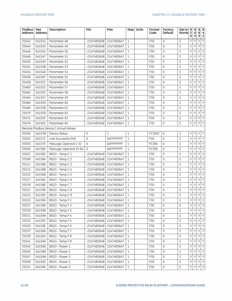
MODBUS MEMORY MAP CHAPTER 11: MODBUS MEMORY MAP
35442 0x1541 Parameter 48 -2147483648 2147483647 1 F30 0 2 Y Y Y Y
35444 0x1543 Parameter 49 -2147483648 2147483647 1 F30 0 2 Y Y Y Y
35446 0x1545 Parameter 50 -2147483648 2147483647 1 F30 0 2 Y Y Y Y
35448 0x1547 Parameter 51 -2147483648 2147483647 1 F30 0 2 Y Y Y Y
35450 0x1549 Parameter 52 -2147483648 2147483647 1 F30 0 2 Y Y Y Y
35452 0x154B Parameter 53 -2147483648 2147483647 1 F30 0 2 Y Y Y Y
35454 0x154D Parameter 54 -2147483648 2147483647 1 F30 0 2 Y Y Y Y
35456 0x154F Parameter 55 -2147483648 2147483647 1 F30 0 2 Y Y Y Y
35458 0x1551 Parameter 56 -2147483648 2147483647 1 F30 0 2 Y Y Y Y
35460 0x1553 Parameter 57 -2147483648 2147483647 1 F30 0 2 Y Y Y Y
35462 0x1555 Parameter 58 -2147483648 2147483647 1 F30 0 2 Y Y Y Y
35464 0x1557 Parameter 59 -2147483648 2147483647 1 F30 0 2 Y Y Y Y
35466 0x1559 Parameter 60 -2147483648 2147483647 1 F30 0 2 Y Y Y Y
35468 0x155B Parameter 61 -2147483648 2147483647 1 F30 0 2 Y Y Y Y
35470 0x155D Parameter 62 -2147483648 2147483647 1 F30 0 2 Y Y Y Y
35472 0x155F Parameter 63 -2147483648 2147483647 1 F30 0 2 Y Y Y Y
35474 0x1561 Parameter 64 -2147483648 2147483647 1 F30 0 2 Y Y Y Y
Remote Modbus Device 1 Actual Values
35500 0x157B Device Status 0 1 1 FC350C 0 1 Y Y Y Y
35501 0x157C Last Successful Poll 0 0xFFFFFFFF 1 F50 0 2 Y Y Y Y
35503 0x157E FlexLogic Operand 1-32 0 0xFFFFFFFF 1 FC394 0 2 Y Y Y Y
35505 0x1580 FlexLogic Operand 33-64 0 0xFFFFFFFF 1 FC395 0 2 Y Y Y Y
35507 0x1582 BSG3 - Temp C 1 -2147483648 2147483647 1 F30 0 2 Y Y Y Y
35509 0x1584 BSG3 - Temp C 2 -2147483648 2147483647 1 F30 0 2 Y Y Y Y
35511 0x1586 BSG3 - Temp C 3 -2147483648 2147483647 1 F30 0 2 Y Y Y Y
35513 0x1588 BSG3 - Temp C 4 -2147483648 2147483647 1 F30 0 2 Y Y Y Y
35515 0x158A BSG3 - Temp C 5 -2147483648 2147483647 1 F30 0 2 Y Y Y Y
35517 0x158C BSG3 - Temp C 6 -2147483648 2147483647 1 F30 0 2 Y Y Y Y
35519 0x158E BSG3 - Temp C 7 -2147483648 2147483647 1 F30 0 2 Y Y Y Y
35521 0x1590 BSG3 - Temp C 8 -2147483648 2147483647 1 F30 0 2 Y Y Y Y
35523 0x1592 BSG3 - Temp C 9 -2147483648 2147483647 1 F30 0 2 Y Y Y Y
35525 0x1594 BSG3 - Temp F 1 -2147483648 2147483647 1 F30 0 2 Y Y Y Y
35527 0x1596 BSG3 - Temp F 2 -2147483648 2147483647 1 F30 0 2 Y Y Y Y
35529 0x1598 BSG3 - Temp F 3 -2147483648 2147483647 1 F30 0 2 Y Y Y Y
35531 0x159A BSG3 - Temp F 4 -2147483648 2147483647 1 F30 0 2 Y Y Y Y
35533 0x159C BSG3 - Temp F 5 -2147483648 2147483647 1 F30 0 2 Y Y Y Y
35535 0x159E BSG3 - Temp F 6 -2147483648 2147483647 1 F30 0 2 Y Y Y Y
35537 0x15A0 BSG3 - Temp F 7 -2147483648 2147483647 1 F30 0 2 Y Y Y Y
35539 0x15A2 BSG3 - Temp F 8 -2147483648 2147483647 1 F30 0 2 Y Y Y Y
35541 0x15A4 BSG3 - Temp F 9 -2147483648 2147483647 1 F30 0 2 Y Y Y Y
35543 0x15A6 BSG3 - Power 1 -2147483648 2147483647 1 F30 0 2 Y Y Y Y
35545 0x15A8 BSG3 - Power 2 -2147483648 2147483647 1 F30 0 2 Y Y Y Y
35547 0x15AA BSG3 - Power 3 -2147483648 2147483647 1 F30 0 2 Y Y Y Y
35549 0x15AC BSG3 - Power 4 -2147483648 2147483647 1 F30 0 2 Y Y Y Y
35551 0x15AE BSG3 - Power 5 -2147483648 2147483647 1 F30 0 2 Y Y Y Y
Modbus Address
Hex Address
Description Min Max Step Units Format Code
Factory Default
Size in Words
850
869
889
845
11-60 8 SERIES PROTECTIVE RELAY PLATFORM – COMMUNICATIONS GUIDE
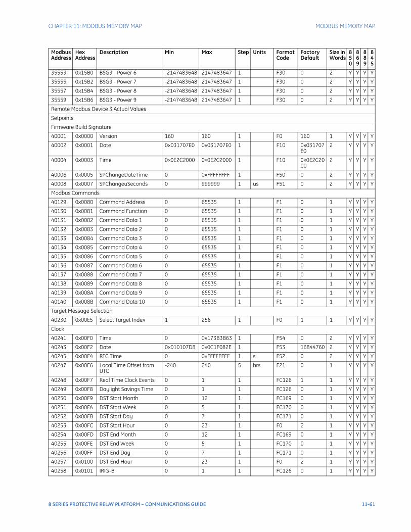
CHAPTER 11: MODBUS MEMORY MAP MODBUS MEMORY MAP
35553 0x15B0 BSG3 - Power 6 -2147483648 2147483647 1 F30 0 2 Y Y Y Y
35555 0x15B2 BSG3 - Power 7 -2147483648 2147483647 1 F30 0 2 Y Y Y Y
35557 0x15B4 BSG3 - Power 8 -2147483648 2147483647 1 F30 0 2 Y Y Y Y
35559 0x15B6 BSG3 - Power 9 -2147483648 2147483647 1 F30 0 2 Y Y Y Y
Remote Modbus Device 3 Actual Values
Setpoints
Firmware Build Signature
40001 0x0000 Version 160 160 1 F0 160 1 Y Y Y Y
40002 0x0001 Date 0x031707E0 0x031707E0 1 F10 0x031707E0
2 Y Y Y Y
40004 0x0003 Time 0x0E2C2000 0x0E2C2000 1 F10 0x0E2C2000
2 Y Y Y Y
40006 0x0005 SPChangeDateTime 0 0xFFFFFFFF 1 F50 0 2 Y Y Y Y
40008 0x0007 SPChangeuSeconds 0 999999 1 us F51 0 2 Y Y Y Y
Modbus Commands
40129 0x0080 Command Address 0 65535 1 F1 0 1 Y Y Y Y
40130 0x0081 Command Function 0 65535 1 F1 0 1 Y Y Y Y
40131 0x0082 Command Data 1 0 65535 1 F1 0 1 Y Y Y Y
40132 0x0083 Command Data 2 0 65535 1 F1 0 1 Y Y Y Y
40133 0x0084 Command Data 3 0 65535 1 F1 0 1 Y Y Y Y
40134 0x0085 Command Data 4 0 65535 1 F1 0 1 Y Y Y Y
40135 0x0086 Command Data 5 0 65535 1 F1 0 1 Y Y Y Y
40136 0x0087 Command Data 6 0 65535 1 F1 0 1 Y Y Y Y
40137 0x0088 Command Data 7 0 65535 1 F1 0 1 Y Y Y Y
40138 0x0089 Command Data 8 0 65535 1 F1 0 1 Y Y Y Y
40139 0x008A Command Data 9 0 65535 1 F1 0 1 Y Y Y Y
40140 0x008B Command Data 10 0 65535 1 F1 0 1 Y Y Y Y
Target Message Selection
40230 0x00E5 Select Target Index 1 256 1 F0 1 1 Y Y Y Y
Clock
40241 0x00F0 Time 0 0x173B3B63 1 F54 0 2 Y Y Y Y
40243 0x00F2 Date 0x010107D8 0x0C1F082E 1 F53 16844760 2 Y Y Y Y
40245 0x00F4 RTC Time 0 0xFFFFFFFF 1 s F52 0 2 Y Y Y Y
40247 0x00F6 Local Time Offset from UTC
-240 240 5 hrs F21 0 1 Y Y Y Y
40248 0x00F7 Real Time Clock Events 0 1 1 FC126 1 1 Y Y Y Y
40249 0x00F8 Daylight Savings Time 0 1 1 FC126 0 1 Y Y Y Y
40250 0x00F9 DST Start Month 0 12 1 FC169 0 1 Y Y Y Y
40251 0x00FA DST Start Week 0 5 1 FC170 0 1 Y Y Y Y
40252 0x00FB DST Start Day 0 7 1 FC171 0 1 Y Y Y Y
40253 0x00FC DST Start Hour 0 23 1 F0 2 1 Y Y Y Y
40254 0x00FD DST End Month 0 12 1 FC169 0 1 Y Y Y Y
40255 0x00FE DST End Week 0 5 1 FC170 0 1 Y Y Y Y
40256 0x00FF DST End Day 0 7 1 FC171 0 1 Y Y Y Y
40257 0x0100 DST End Hour 0 23 1 F0 2 1 Y Y Y Y
40258 0x0101 IRIG-B 0 1 1 FC126 0 1 Y Y Y Y
Modbus Address
Hex Address
Description Min Max Step Units Format Code
Factory Default
Size in Words
850
869
889
845
8 SERIES PROTECTIVE RELAY PLATFORM – COMMUNICATIONS GUIDE 11-61

MODBUS MEMORY MAP CHAPTER 11: MODBUS MEMORY MAP
Precision Time Protocol
40270 0x010D Port 4 PTP Function 0 1 1 FC126 0 1 Y Y Y Y
40271 0x010E Port 4 Path Delay Adder 0 60000 1 ns F0 0 1 Y Y Y Y
40272 0x010F Port4 Path Delay Asymmetry
-1000 1000 1 ns F20 0 1 Y Y Y Y
40273 0x0110 Port 5 PTP Function 0 1 1 FC126 0 1 Y Y Y Y
40274 0x0111 Port 5 Path Delay Adder 0 60000 1 ns F0 0 1 Y Y Y Y
40275 0x0112 Port5 Path Delay Asymmetry
-1000 1000 1 ns F20 0 1 Y Y Y Y
40276 0x0113 Strict Power Profile 0 1 1 FC126 1 1 Y Y Y Y
40277 0x0114 PTP Domain Number 0 255 1 F0 0 1 Y Y Y Y
40278 0x0115 PTP VLAN Priority 0 7 1 F0 4 1 Y Y Y Y
40279 0x0116 PTP VLAN ID 0 4095 1 F0 0 1 Y Y Y Y
40280 0x0117 PTP Priority 1 2 1 F0 1 1 Y Y Y Y
SNTP
40300 0x012B SNTP Function 0 1 1 FC126 0 1 Y Y Y Y
40301 0x012C SNTP Server IP Address 0 0xFFFFFFFF 1 F70 0 2 Y Y Y Y
40303 0x012E SNTP UDP Port Number 0 65535 1 F0A 123 1 Y Y Y Y
User Map Setpoints
40524 0x020B User Map Address 1 30001 49999 1 F0 30712 1 Y Y Y Y
40525 0x020C User Map Address 2 30001 49999 1 F0 30713 1 Y Y Y Y
40526 0x020D User Map Address 3 30001 49999 1 F0 30708 1 Y Y Y Y
40527 0x020E User Map Address 4 30001 49999 1 F0 30709 1 Y Y Y Y
40528 0x020F User Map Address 5 30001 49999 1 F0 30700 1 Y Y Y Y
40529 0x0210 User Map Address 6 30001 49999 1 F0 30701 1 Y Y Y Y
40530 0x0211 User Map Address 7 30001 49999 1 F0 30706 1 Y Y Y Y
40531 0x0212 User Map Address 8 30001 49999 1 F0 30707 1 Y Y Y Y
40532 0x0213 User Map Address 9 30001 49999 1 F0 30714 1 Y Y Y Y
40533 0x0214 User Map Address 10 30001 49999 1 F0 30715 1 Y Y Y Y
40534 0x0215 User Map Address 11 30001 49999 1 F0 30722 1 Y Y Y Y
40535 0x0216 User Map Address 12 30001 49999 1 F0 30723 1 Y Y Y Y
40536 0x0217 User Map Address 13 30001 49999 1 F0 30734 1 Y Y Y Y
40537 0x0218 User Map Address 14 30001 49999 1 F0 30735 1 Y Y Y Y
40538 0x0219 User Map Address 15 30001 49999 1 F0 30742 1 Y Y Y Y
40539 0x021A User Map Address 16 30001 49999 1 F0 30743 1 Y Y Y Y
40540 0x021B User Map Address 17 30001 49999 1 F0 31270 1 Y Y Y Y
40541 0x021C User Map Address 18 30001 49999 1 F0 31271 1 Y Y Y Y
40542 0x021D User Map Address 19 30001 49999 1 F0 31272 1 Y Y Y Y
40543 0x021E User Map Address 20 30001 49999 1 F0 31273 1 Y Y Y Y
40544 0x021F User Map Address 21 30001 49999 1 F0 31274 1 Y Y Y Y
40545 0x0220 User Map Address 22 30001 49999 1 F0 31275 1 Y Y Y Y
40546 0x0221 User Map Address 23 30001 49999 1 F0 31278 1 Y Y Y Y
40547 0x0222 User Map Address 24 30001 49999 1 F0 31279 1 Y Y Y Y
40548 0x0223 User Map Address 25 30001 49999 1 F0 31295 1 Y Y Y Y
40549 0x0224 User Map Address 26 30001 49999 1 F0 31296 1 Y Y Y Y
40550 0x0225 User Map Address 27 30001 49999 1 F0 31276 1 Y Y Y Y
Modbus Address
Hex Address
Description Min Max Step Units Format Code
Factory Default
Size in Words
850
869
889
845
11-62 8 SERIES PROTECTIVE RELAY PLATFORM – COMMUNICATIONS GUIDE
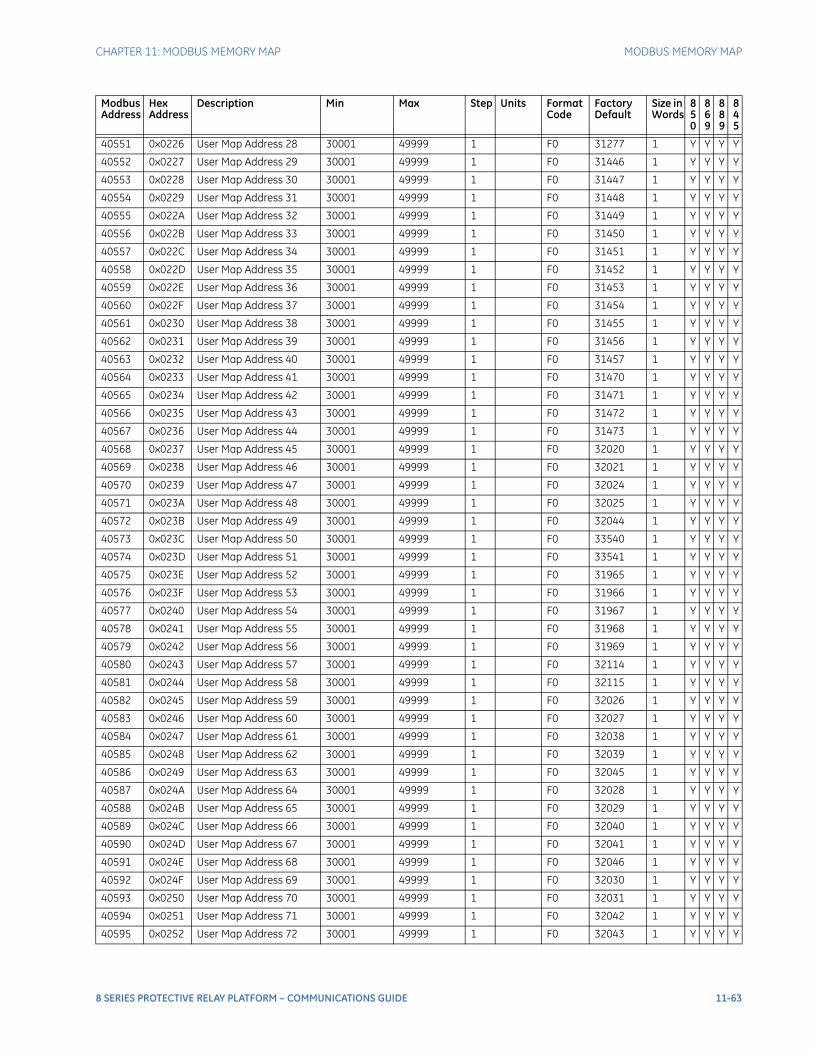
CHAPTER 11: MODBUS MEMORY MAP MODBUS MEMORY MAP
40551 0x0226 User Map Address 28 30001 49999 1 F0 31277 1 Y Y Y Y
40552 0x0227 User Map Address 29 30001 49999 1 F0 31446 1 Y Y Y Y
40553 0x0228 User Map Address 30 30001 49999 1 F0 31447 1 Y Y Y Y
40554 0x0229 User Map Address 31 30001 49999 1 F0 31448 1 Y Y Y Y
40555 0x022A User Map Address 32 30001 49999 1 F0 31449 1 Y Y Y Y
40556 0x022B User Map Address 33 30001 49999 1 F0 31450 1 Y Y Y Y
40557 0x022C User Map Address 34 30001 49999 1 F0 31451 1 Y Y Y Y
40558 0x022D User Map Address 35 30001 49999 1 F0 31452 1 Y Y Y Y
40559 0x022E User Map Address 36 30001 49999 1 F0 31453 1 Y Y Y Y
40560 0x022F User Map Address 37 30001 49999 1 F0 31454 1 Y Y Y Y
40561 0x0230 User Map Address 38 30001 49999 1 F0 31455 1 Y Y Y Y
40562 0x0231 User Map Address 39 30001 49999 1 F0 31456 1 Y Y Y Y
40563 0x0232 User Map Address 40 30001 49999 1 F0 31457 1 Y Y Y Y
40564 0x0233 User Map Address 41 30001 49999 1 F0 31470 1 Y Y Y Y
40565 0x0234 User Map Address 42 30001 49999 1 F0 31471 1 Y Y Y Y
40566 0x0235 User Map Address 43 30001 49999 1 F0 31472 1 Y Y Y Y
40567 0x0236 User Map Address 44 30001 49999 1 F0 31473 1 Y Y Y Y
40568 0x0237 User Map Address 45 30001 49999 1 F0 32020 1 Y Y Y Y
40569 0x0238 User Map Address 46 30001 49999 1 F0 32021 1 Y Y Y Y
40570 0x0239 User Map Address 47 30001 49999 1 F0 32024 1 Y Y Y Y
40571 0x023A User Map Address 48 30001 49999 1 F0 32025 1 Y Y Y Y
40572 0x023B User Map Address 49 30001 49999 1 F0 32044 1 Y Y Y Y
40573 0x023C User Map Address 50 30001 49999 1 F0 33540 1 Y Y Y Y
40574 0x023D User Map Address 51 30001 49999 1 F0 33541 1 Y Y Y Y
40575 0x023E User Map Address 52 30001 49999 1 F0 31965 1 Y Y Y Y
40576 0x023F User Map Address 53 30001 49999 1 F0 31966 1 Y Y Y Y
40577 0x0240 User Map Address 54 30001 49999 1 F0 31967 1 Y Y Y Y
40578 0x0241 User Map Address 55 30001 49999 1 F0 31968 1 Y Y Y Y
40579 0x0242 User Map Address 56 30001 49999 1 F0 31969 1 Y Y Y Y
40580 0x0243 User Map Address 57 30001 49999 1 F0 32114 1 Y Y Y Y
40581 0x0244 User Map Address 58 30001 49999 1 F0 32115 1 Y Y Y Y
40582 0x0245 User Map Address 59 30001 49999 1 F0 32026 1 Y Y Y Y
40583 0x0246 User Map Address 60 30001 49999 1 F0 32027 1 Y Y Y Y
40584 0x0247 User Map Address 61 30001 49999 1 F0 32038 1 Y Y Y Y
40585 0x0248 User Map Address 62 30001 49999 1 F0 32039 1 Y Y Y Y
40586 0x0249 User Map Address 63 30001 49999 1 F0 32045 1 Y Y Y Y
40587 0x024A User Map Address 64 30001 49999 1 F0 32028 1 Y Y Y Y
40588 0x024B User Map Address 65 30001 49999 1 F0 32029 1 Y Y Y Y
40589 0x024C User Map Address 66 30001 49999 1 F0 32040 1 Y Y Y Y
40590 0x024D User Map Address 67 30001 49999 1 F0 32041 1 Y Y Y Y
40591 0x024E User Map Address 68 30001 49999 1 F0 32046 1 Y Y Y Y
40592 0x024F User Map Address 69 30001 49999 1 F0 32030 1 Y Y Y Y
40593 0x0250 User Map Address 70 30001 49999 1 F0 32031 1 Y Y Y Y
40594 0x0251 User Map Address 71 30001 49999 1 F0 32042 1 Y Y Y Y
40595 0x0252 User Map Address 72 30001 49999 1 F0 32043 1 Y Y Y Y
Modbus Address
Hex Address
Description Min Max Step Units Format Code
Factory Default
Size in Words
850
869
889
845
8 SERIES PROTECTIVE RELAY PLATFORM – COMMUNICATIONS GUIDE 11-63
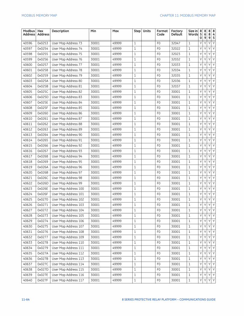
MODBUS MEMORY MAP CHAPTER 11: MODBUS MEMORY MAP
40596 0x0253 User Map Address 73 30001 49999 1 F0 32047 1 Y Y Y Y
40597 0x0254 User Map Address 74 30001 49999 1 F0 32022 1 Y Y Y Y
40598 0x0255 User Map Address 75 30001 49999 1 F0 32023 1 Y Y Y Y
40599 0x0256 User Map Address 76 30001 49999 1 F0 32032 1 Y Y Y Y
40600 0x0257 User Map Address 77 30001 49999 1 F0 32033 1 Y Y Y Y
40601 0x0258 User Map Address 78 30001 49999 1 F0 32034 1 Y Y Y Y
40602 0x0259 User Map Address 79 30001 49999 1 F0 32035 1 Y Y Y Y
40603 0x025A User Map Address 80 30001 49999 1 F0 32036 1 Y Y Y Y
40604 0x025B User Map Address 81 30001 49999 1 F0 32037 1 Y Y Y Y
40605 0x025C User Map Address 82 30001 49999 1 F0 30001 1 Y Y Y Y
40606 0x025D User Map Address 83 30001 49999 1 F0 30001 1 Y Y Y Y
40607 0x025E User Map Address 84 30001 49999 1 F0 30001 1 Y Y Y Y
40608 0x025F User Map Address 85 30001 49999 1 F0 30001 1 Y Y Y Y
40609 0x0260 User Map Address 86 30001 49999 1 F0 30001 1 Y Y Y Y
40610 0x0261 User Map Address 87 30001 49999 1 F0 30001 1 Y Y Y Y
40611 0x0262 User Map Address 88 30001 49999 1 F0 30001 1 Y Y Y Y
40612 0x0263 User Map Address 89 30001 49999 1 F0 30001 1 Y Y Y Y
40613 0x0264 User Map Address 90 30001 49999 1 F0 30001 1 Y Y Y Y
40614 0x0265 User Map Address 91 30001 49999 1 F0 30001 1 Y Y Y Y
40615 0x0266 User Map Address 92 30001 49999 1 F0 30001 1 Y Y Y Y
40616 0x0267 User Map Address 93 30001 49999 1 F0 30001 1 Y Y Y Y
40617 0x0268 User Map Address 94 30001 49999 1 F0 30001 1 Y Y Y Y
40618 0x0269 User Map Address 95 30001 49999 1 F0 30001 1 Y Y Y Y
40619 0x026A User Map Address 96 30001 49999 1 F0 30001 1 Y Y Y Y
40620 0x026B User Map Address 97 30001 49999 1 F0 30001 1 Y Y Y Y
40621 0x026C User Map Address 98 30001 49999 1 F0 30001 1 Y Y Y Y
40622 0x026D User Map Address 99 30001 49999 1 F0 30001 1 Y Y Y Y
40623 0x026E User Map Address 100 30001 49999 1 F0 30001 1 Y Y Y Y
40624 0x026F User Map Address 101 30001 49999 1 F0 30001 1 Y Y Y Y
40625 0x0270 User Map Address 102 30001 49999 1 F0 30001 1 Y Y Y Y
40626 0x0271 User Map Address 103 30001 49999 1 F0 30001 1 Y Y Y Y
40627 0x0272 User Map Address 104 30001 49999 1 F0 30001 1 Y Y Y Y
40628 0x0273 User Map Address 105 30001 49999 1 F0 30001 1 Y Y Y Y
40629 0x0274 User Map Address 106 30001 49999 1 F0 30001 1 Y Y Y Y
40630 0x0275 User Map Address 107 30001 49999 1 F0 30001 1 Y Y Y Y
40631 0x0276 User Map Address 108 30001 49999 1 F0 30001 1 Y Y Y Y
40632 0x0277 User Map Address 109 30001 49999 1 F0 30001 1 Y Y Y Y
40633 0x0278 User Map Address 110 30001 49999 1 F0 30001 1 Y Y Y Y
40634 0x0279 User Map Address 111 30001 49999 1 F0 30001 1 Y Y Y Y
40635 0x027A User Map Address 112 30001 49999 1 F0 30001 1 Y Y Y Y
40636 0x027B User Map Address 113 30001 49999 1 F0 30001 1 Y Y Y Y
40637 0x027C User Map Address 114 30001 49999 1 F0 30001 1 Y Y Y Y
40638 0x027D User Map Address 115 30001 49999 1 F0 30001 1 Y Y Y Y
40639 0x027E User Map Address 116 30001 49999 1 F0 30001 1 Y Y Y Y
40640 0x027F User Map Address 117 30001 49999 1 F0 30001 1 Y Y Y Y
Modbus Address
Hex Address
Description Min Max Step Units Format Code
Factory Default
Size in Words
850
869
889
845
11-64 8 SERIES PROTECTIVE RELAY PLATFORM – COMMUNICATIONS GUIDE
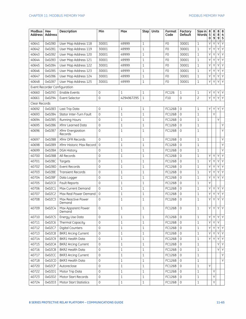
CHAPTER 11: MODBUS MEMORY MAP MODBUS MEMORY MAP
40641 0x0280 User Map Address 118 30001 49999 1 F0 30001 1 Y Y Y Y
40642 0x0281 User Map Address 119 30001 49999 1 F0 30001 1 Y Y Y Y
40643 0x0282 User Map Address 120 30001 49999 1 F0 30001 1 Y Y Y Y
40644 0x0283 User Map Address 121 30001 49999 1 F0 30001 1 Y Y Y Y
40645 0x0284 User Map Address 122 30001 49999 1 F0 30001 1 Y Y Y Y
40646 0x0285 User Map Address 123 30001 49999 1 F0 30001 1 Y Y Y Y
40647 0x0286 User Map Address 124 30001 49999 1 F0 30001 1 Y Y Y Y
40648 0x0287 User Map Address 125 30001 49999 1 F0 30001 1 Y Y Y Y
Event Recorder Configuration
40660 0x0293 Enable Events 0 1 1 FC126 1 1 Y Y Y Y
40661 0x0294 Event Selector 0 4294967295 1 F10 0 2 Y Y Y Y
Clear Records
40692 0x02B3 Last Trip Data 0 1 1 FC126B 0 1 Y Y Y Y
40693 0x02B4 Stator Inter-Turn Fault 0 1 1 FC126B 0 1 Y
40694 0x02B5 Running Hours 0 1 1 FC126B 0 1 Y
40695 0x02B6 Xfmr Learned Data 0 1 1 FC126B 0 1 Y
40696 0x02B7 Xfmr Energization Records
0 1 1 FC126B 0 1 Y
40697 0x02B8 Xfmr DFR Records 0 1 1 FC126B 0 1 Y
40698 0x02B9 Xfmr Historic Max Record 0 1 1 FC126B 0 1 Y
40699 0x02BA DGA History 0 1 1 FC126B 0 1 Y
40700 0x02BB All Records 0 1 1 FC126B 0 1 Y Y Y Y
40701 0x02BC Targets 0 1 1 FC126B 0 1 Y Y Y Y
40702 0x02BD Event Records 0 1 1 FC126B 0 1 Y Y Y Y
40703 0x02BE Transient Records 0 1 1 FC126B 0 1 Y Y Y Y
40704 0x02BF Data Logger 0 1 1 FC126B 0 1 Y Y Y Y
40705 0x02C0 Fault Reports 0 1 1 FC126B 0 1 Y
40706 0x02C1 Max Current Demand 0 1 1 FC126B 0 1 Y Y Y Y
40707 0x02C2 Max Real Power Demand 0 1 1 FC126B 0 1 Y Y Y Y
40708 0x02C3 Max Reactive Power Demand
0 1 1 FC126B 0 1 Y Y Y Y
40709 0x02C4 Max Apparent Power Demand
0 1 1 FC126B 0 1 Y Y Y Y
40710 0x02C5 Energy Use Data 0 1 1 FC126B 0 1 Y Y Y Y
40711 0x02C6 Thermal Capacity 0 1 1 FC126B 0 1 Y Y Y
40712 0x02C7 Digital Counters 0 1 1 FC126B 0 1 Y Y Y Y
40713 0x02C8 BKR1 Arcing Current 0 1 1 FC126B 0 1 Y Y Y Y
40714 0x02C9 BKR1 Health Data 0 1 1 FC126B 0 1 Y Y Y Y
40715 0x02CA BKR2 Arcing Current 0 1 1 FC126B 0 1 Y Y
40716 0x02CB BKR2 Health Data 0 1 1 FC126B 0 1 Y Y
40717 0x02CC BKR3 Arcing Current 0 1 1 FC126B 0 1 Y
40718 0x02CD BKR3 Health Data 0 1 1 FC126B 0 1 Y
40720 0x02CF Autoreclose 0 1 1 FC126B 0 1 Y
40722 0x02D1 Motor Trip Data 0 1 1 FC126B 0 1 Y
40723 0x02D2 Motor Start Records 0 1 1 FC126B 0 1 Y
40724 0x02D3 Motor Start Statistics 0 1 1 FC126B 0 1 Y
Modbus Address
Hex Address
Description Min Max Step Units Format Code
Factory Default
Size in Words
850
869
889
845
8 SERIES PROTECTIVE RELAY PLATFORM – COMMUNICATIONS GUIDE 11-65
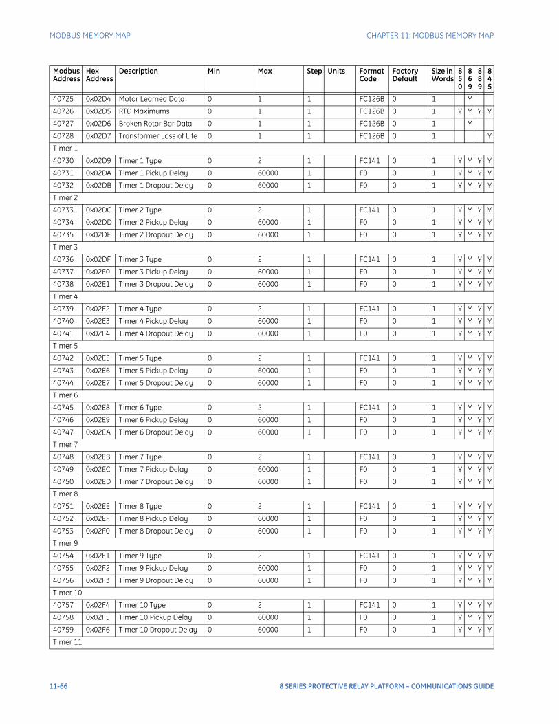
MODBUS MEMORY MAP CHAPTER 11: MODBUS MEMORY MAP
40725 0x02D4 Motor Learned Data 0 1 1 FC126B 0 1 Y
40726 0x02D5 RTD Maximums 0 1 1 FC126B 0 1 Y Y Y Y
40727 0x02D6 Broken Rotor Bar Data 0 1 1 FC126B 0 1 Y
40728 0x02D7 Transformer Loss of Life 0 1 1 FC126B 0 1 Y
Timer 1
40730 0x02D9 Timer 1 Type 0 2 1 FC141 0 1 Y Y Y Y
40731 0x02DA Timer 1 Pickup Delay 0 60000 1 F0 0 1 Y Y Y Y
40732 0x02DB Timer 1 Dropout Delay 0 60000 1 F0 0 1 Y Y Y Y
Timer 2
40733 0x02DC Timer 2 Type 0 2 1 FC141 0 1 Y Y Y Y
40734 0x02DD Timer 2 Pickup Delay 0 60000 1 F0 0 1 Y Y Y Y
40735 0x02DE Timer 2 Dropout Delay 0 60000 1 F0 0 1 Y Y Y Y
Timer 3
40736 0x02DF Timer 3 Type 0 2 1 FC141 0 1 Y Y Y Y
40737 0x02E0 Timer 3 Pickup Delay 0 60000 1 F0 0 1 Y Y Y Y
40738 0x02E1 Timer 3 Dropout Delay 0 60000 1 F0 0 1 Y Y Y Y
Timer 4
40739 0x02E2 Timer 4 Type 0 2 1 FC141 0 1 Y Y Y Y
40740 0x02E3 Timer 4 Pickup Delay 0 60000 1 F0 0 1 Y Y Y Y
40741 0x02E4 Timer 4 Dropout Delay 0 60000 1 F0 0 1 Y Y Y Y
Timer 5
40742 0x02E5 Timer 5 Type 0 2 1 FC141 0 1 Y Y Y Y
40743 0x02E6 Timer 5 Pickup Delay 0 60000 1 F0 0 1 Y Y Y Y
40744 0x02E7 Timer 5 Dropout Delay 0 60000 1 F0 0 1 Y Y Y Y
Timer 6
40745 0x02E8 Timer 6 Type 0 2 1 FC141 0 1 Y Y Y Y
40746 0x02E9 Timer 6 Pickup Delay 0 60000 1 F0 0 1 Y Y Y Y
40747 0x02EA Timer 6 Dropout Delay 0 60000 1 F0 0 1 Y Y Y Y
Timer 7
40748 0x02EB Timer 7 Type 0 2 1 FC141 0 1 Y Y Y Y
40749 0x02EC Timer 7 Pickup Delay 0 60000 1 F0 0 1 Y Y Y Y
40750 0x02ED Timer 7 Dropout Delay 0 60000 1 F0 0 1 Y Y Y Y
Timer 8
40751 0x02EE Timer 8 Type 0 2 1 FC141 0 1 Y Y Y Y
40752 0x02EF Timer 8 Pickup Delay 0 60000 1 F0 0 1 Y Y Y Y
40753 0x02F0 Timer 8 Dropout Delay 0 60000 1 F0 0 1 Y Y Y Y
Timer 9
40754 0x02F1 Timer 9 Type 0 2 1 FC141 0 1 Y Y Y Y
40755 0x02F2 Timer 9 Pickup Delay 0 60000 1 F0 0 1 Y Y Y Y
40756 0x02F3 Timer 9 Dropout Delay 0 60000 1 F0 0 1 Y Y Y Y
Timer 10
40757 0x02F4 Timer 10 Type 0 2 1 FC141 0 1 Y Y Y Y
40758 0x02F5 Timer 10 Pickup Delay 0 60000 1 F0 0 1 Y Y Y Y
40759 0x02F6 Timer 10 Dropout Delay 0 60000 1 F0 0 1 Y Y Y Y
Timer 11
Modbus Address
Hex Address
Description Min Max Step Units Format Code
Factory Default
Size in Words
850
869
889
845
11-66 8 SERIES PROTECTIVE RELAY PLATFORM – COMMUNICATIONS GUIDE
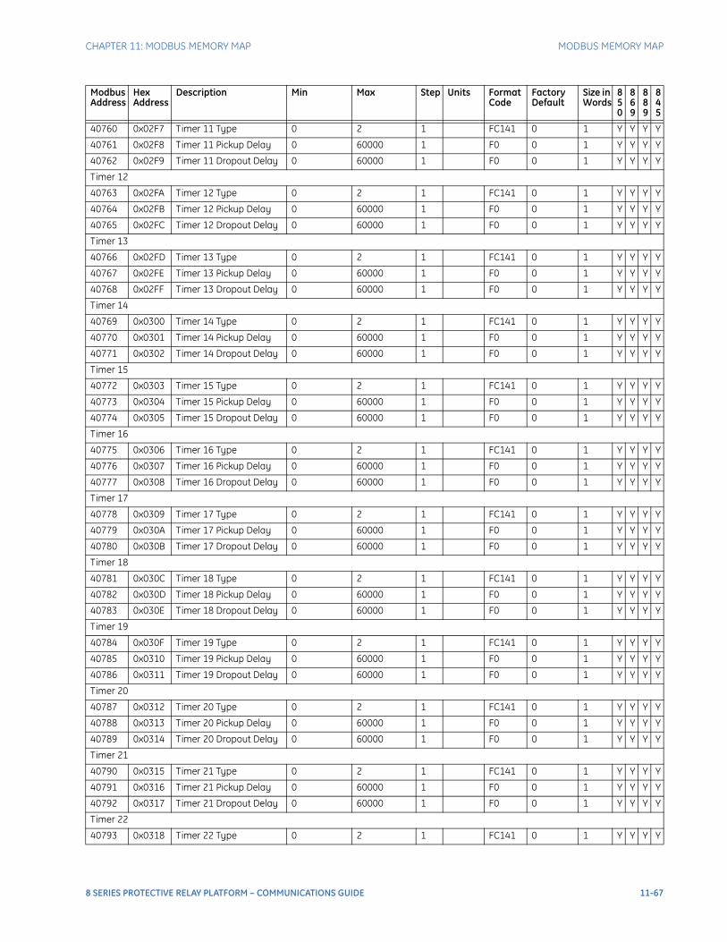
CHAPTER 11: MODBUS MEMORY MAP MODBUS MEMORY MAP
40760 0x02F7 Timer 11 Type 0 2 1 FC141 0 1 Y Y Y Y
40761 0x02F8 Timer 11 Pickup Delay 0 60000 1 F0 0 1 Y Y Y Y
40762 0x02F9 Timer 11 Dropout Delay 0 60000 1 F0 0 1 Y Y Y Y
Timer 12
40763 0x02FA Timer 12 Type 0 2 1 FC141 0 1 Y Y Y Y
40764 0x02FB Timer 12 Pickup Delay 0 60000 1 F0 0 1 Y Y Y Y
40765 0x02FC Timer 12 Dropout Delay 0 60000 1 F0 0 1 Y Y Y Y
Timer 13
40766 0x02FD Timer 13 Type 0 2 1 FC141 0 1 Y Y Y Y
40767 0x02FE Timer 13 Pickup Delay 0 60000 1 F0 0 1 Y Y Y Y
40768 0x02FF Timer 13 Dropout Delay 0 60000 1 F0 0 1 Y Y Y Y
Timer 14
40769 0x0300 Timer 14 Type 0 2 1 FC141 0 1 Y Y Y Y
40770 0x0301 Timer 14 Pickup Delay 0 60000 1 F0 0 1 Y Y Y Y
40771 0x0302 Timer 14 Dropout Delay 0 60000 1 F0 0 1 Y Y Y Y
Timer 15
40772 0x0303 Timer 15 Type 0 2 1 FC141 0 1 Y Y Y Y
40773 0x0304 Timer 15 Pickup Delay 0 60000 1 F0 0 1 Y Y Y Y
40774 0x0305 Timer 15 Dropout Delay 0 60000 1 F0 0 1 Y Y Y Y
Timer 16
40775 0x0306 Timer 16 Type 0 2 1 FC141 0 1 Y Y Y Y
40776 0x0307 Timer 16 Pickup Delay 0 60000 1 F0 0 1 Y Y Y Y
40777 0x0308 Timer 16 Dropout Delay 0 60000 1 F0 0 1 Y Y Y Y
Timer 17
40778 0x0309 Timer 17 Type 0 2 1 FC141 0 1 Y Y Y Y
40779 0x030A Timer 17 Pickup Delay 0 60000 1 F0 0 1 Y Y Y Y
40780 0x030B Timer 17 Dropout Delay 0 60000 1 F0 0 1 Y Y Y Y
Timer 18
40781 0x030C Timer 18 Type 0 2 1 FC141 0 1 Y Y Y Y
40782 0x030D Timer 18 Pickup Delay 0 60000 1 F0 0 1 Y Y Y Y
40783 0x030E Timer 18 Dropout Delay 0 60000 1 F0 0 1 Y Y Y Y
Timer 19
40784 0x030F Timer 19 Type 0 2 1 FC141 0 1 Y Y Y Y
40785 0x0310 Timer 19 Pickup Delay 0 60000 1 F0 0 1 Y Y Y Y
40786 0x0311 Timer 19 Dropout Delay 0 60000 1 F0 0 1 Y Y Y Y
Timer 20
40787 0x0312 Timer 20 Type 0 2 1 FC141 0 1 Y Y Y Y
40788 0x0313 Timer 20 Pickup Delay 0 60000 1 F0 0 1 Y Y Y Y
40789 0x0314 Timer 20 Dropout Delay 0 60000 1 F0 0 1 Y Y Y Y
Timer 21
40790 0x0315 Timer 21 Type 0 2 1 FC141 0 1 Y Y Y Y
40791 0x0316 Timer 21 Pickup Delay 0 60000 1 F0 0 1 Y Y Y Y
40792 0x0317 Timer 21 Dropout Delay 0 60000 1 F0 0 1 Y Y Y Y
Timer 22
40793 0x0318 Timer 22 Type 0 2 1 FC141 0 1 Y Y Y Y
Modbus Address
Hex Address
Description Min Max Step Units Format Code
Factory Default
Size in Words
850
869
889
845
8 SERIES PROTECTIVE RELAY PLATFORM – COMMUNICATIONS GUIDE 11-67
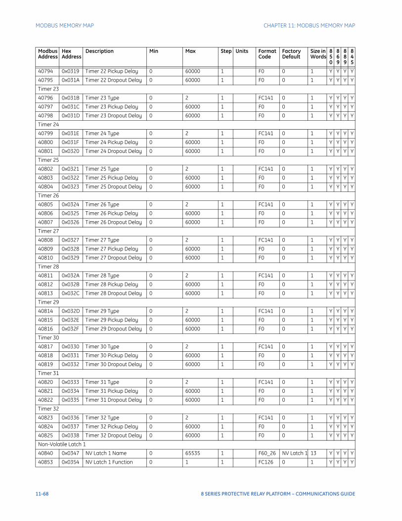
MODBUS MEMORY MAP CHAPTER 11: MODBUS MEMORY MAP
40794 0x0319 Timer 22 Pickup Delay 0 60000 1 F0 0 1 Y Y Y Y
40795 0x031A Timer 22 Dropout Delay 0 60000 1 F0 0 1 Y Y Y Y
Timer 23
40796 0x031B Timer 23 Type 0 2 1 FC141 0 1 Y Y Y Y
40797 0x031C Timer 23 Pickup Delay 0 60000 1 F0 0 1 Y Y Y Y
40798 0x031D Timer 23 Dropout Delay 0 60000 1 F0 0 1 Y Y Y Y
Timer 24
40799 0x031E Timer 24 Type 0 2 1 FC141 0 1 Y Y Y Y
40800 0x031F Timer 24 Pickup Delay 0 60000 1 F0 0 1 Y Y Y Y
40801 0x0320 Timer 24 Dropout Delay 0 60000 1 F0 0 1 Y Y Y Y
Timer 25
40802 0x0321 Timer 25 Type 0 2 1 FC141 0 1 Y Y Y Y
40803 0x0322 Timer 25 Pickup Delay 0 60000 1 F0 0 1 Y Y Y Y
40804 0x0323 Timer 25 Dropout Delay 0 60000 1 F0 0 1 Y Y Y Y
Timer 26
40805 0x0324 Timer 26 Type 0 2 1 FC141 0 1 Y Y Y Y
40806 0x0325 Timer 26 Pickup Delay 0 60000 1 F0 0 1 Y Y Y Y
40807 0x0326 Timer 26 Dropout Delay 0 60000 1 F0 0 1 Y Y Y Y
Timer 27
40808 0x0327 Timer 27 Type 0 2 1 FC141 0 1 Y Y Y Y
40809 0x0328 Timer 27 Pickup Delay 0 60000 1 F0 0 1 Y Y Y Y
40810 0x0329 Timer 27 Dropout Delay 0 60000 1 F0 0 1 Y Y Y Y
Timer 28
40811 0x032A Timer 28 Type 0 2 1 FC141 0 1 Y Y Y Y
40812 0x032B Timer 28 Pickup Delay 0 60000 1 F0 0 1 Y Y Y Y
40813 0x032C Timer 28 Dropout Delay 0 60000 1 F0 0 1 Y Y Y Y
Timer 29
40814 0x032D Timer 29 Type 0 2 1 FC141 0 1 Y Y Y Y
40815 0x032E Timer 29 Pickup Delay 0 60000 1 F0 0 1 Y Y Y Y
40816 0x032F Timer 29 Dropout Delay 0 60000 1 F0 0 1 Y Y Y Y
Timer 30
40817 0x0330 Timer 30 Type 0 2 1 FC141 0 1 Y Y Y Y
40818 0x0331 Timer 30 Pickup Delay 0 60000 1 F0 0 1 Y Y Y Y
40819 0x0332 Timer 30 Dropout Delay 0 60000 1 F0 0 1 Y Y Y Y
Timer 31
40820 0x0333 Timer 31 Type 0 2 1 FC141 0 1 Y Y Y Y
40821 0x0334 Timer 31 Pickup Delay 0 60000 1 F0 0 1 Y Y Y Y
40822 0x0335 Timer 31 Dropout Delay 0 60000 1 F0 0 1 Y Y Y Y
Timer 32
40823 0x0336 Timer 32 Type 0 2 1 FC141 0 1 Y Y Y Y
40824 0x0337 Timer 32 Pickup Delay 0 60000 1 F0 0 1 Y Y Y Y
40825 0x0338 Timer 32 Dropout Delay 0 60000 1 F0 0 1 Y Y Y Y
Non-Volatile Latch 1
40840 0x0347 NV Latch 1 Name 0 65535 1 F60_26 NV Latch 1 13 Y Y Y Y
40853 0x0354 NV Latch 1 Function 0 1 1 FC126 0 1 Y Y Y Y
Modbus Address
Hex Address
Description Min Max Step Units Format Code
Factory Default
Size in Words
850
869
889
845
11-68 8 SERIES PROTECTIVE RELAY PLATFORM – COMMUNICATIONS GUIDE

CHAPTER 11: MODBUS MEMORY MAP MODBUS MEMORY MAP
40854 0x0355 NV Latch 1 Type 0 1 1 FC271 0 1 Y Y Y Y
40855 0x0356 NV Latch 1 Set 0 0xFFFFFFFF 1 FC142 0 2 Y Y Y Y
40857 0x0358 NV Latch 1 Reset 0 0xFFFFFFFF 1 FC142 0 2 Y Y Y Y
40859 0x035A NV Latch 1 Events 0 1 1 FC126 1 1 Y Y Y Y
40860 0x035B NV Latch 1 Targets 0 2 1 FC101 1 1 Y Y Y Y
Non-Volatile Latch 2
40861 0x035C NV Latch 2 Name 0 65535 1 F60_26 NV Latch 2 13 Y Y Y Y
40874 0x0369 NV Latch 2 Function 0 1 1 FC126 0 1 Y Y Y Y
40875 0x036A NV Latch 2 Type 0 1 1 FC271 0 1 Y Y Y Y
40876 0x036B NV Latch 2 Set 0 0xFFFFFFFF 1 FC142 0 2 Y Y Y Y
40878 0x036D NV Latch 2 Reset 0 0xFFFFFFFF 1 FC142 0 2 Y Y Y Y
40880 0x036F NV Latch 2 Events 0 1 1 FC126 1 1 Y Y Y Y
40881 0x0370 NV Latch 2 Targets 0 2 1 FC101 1 1 Y Y Y Y
Non-Volatile Latch 3
40882 0x0371 NV Latch 3 Name 0 65535 1 F60_26 NV Latch 3 13 Y Y Y Y
40895 0x037E NV Latch 3 Function 0 1 1 FC126 0 1 Y Y Y Y
40896 0x037F NV Latch 3 Type 0 1 1 FC271 0 1 Y Y Y Y
40897 0x0380 NV Latch 3 Set 0 0xFFFFFFFF 1 FC142 0 2 Y Y Y Y
40899 0x0382 NV Latch 3 Reset 0 0xFFFFFFFF 1 FC142 0 2 Y Y Y Y
40901 0x0384 NV Latch 3 Events 0 1 1 FC126 1 1 Y Y Y Y
40902 0x0385 NV Latch 3 Targets 0 2 1 FC101 1 1 Y Y Y Y
Non-Volatile Latch 4
40903 0x0386 NV Latch 4 Name 0 65535 1 F60_26 NV Latch 4 13 Y Y Y Y
40916 0x0393 NV Latch 4 Function 0 1 1 FC126 0 1 Y Y Y Y
40917 0x0394 NV Latch 4 Type 0 1 1 FC271 0 1 Y Y Y Y
40918 0x0395 NV Latch 4 Set 0 0xFFFFFFFF 1 FC142 0 2 Y Y Y Y
40920 0x0397 NV Latch 4 Reset 0 0xFFFFFFFF 1 FC142 0 2 Y Y Y Y
40922 0x0399 NV Latch 4 Events 0 1 1 FC126 1 1 Y Y Y Y
40923 0x039A NV Latch 4 Targets 0 2 1 FC101 1 1 Y Y Y Y
Non-Volatile Latch 5
40924 0x039B NV Latch 5 Name 0 65535 1 F60_26 NV Latch 5 13 Y Y Y Y
40937 0x03A8 NV Latch 5 Function 0 1 1 FC126 0 1 Y Y Y Y
40938 0x03A9 NV Latch 5 Type 0 1 1 FC271 0 1 Y Y Y Y
40939 0x03AA NV Latch 5 Set 0 0xFFFFFFFF 1 FC142 0 2 Y Y Y Y
40941 0x03AC NV Latch 5 Reset 0 0xFFFFFFFF 1 FC142 0 2 Y Y Y Y
40943 0x03AE NV Latch 5 Events 0 1 1 FC126 1 1 Y Y Y Y
40944 0x03AF NV Latch 5 Targets 0 2 1 FC101 1 1 Y Y Y Y
Non-Volatile Latch 6
40945 0x03B0 NV Latch 6 Name 0 65535 1 F60_26 NV Latch 6 13 Y Y Y Y
40958 0x03BD NV Latch 6 Function 0 1 1 FC126 0 1 Y Y Y Y
40959 0x03BE NV Latch 6 Type 0 1 1 FC271 0 1 Y Y Y Y
40960 0x03BF NV Latch 6 Set 0 0xFFFFFFFF 1 FC142 0 2 Y Y Y Y
40962 0x03C1 NV Latch 6 Reset 0 0xFFFFFFFF 1 FC142 0 2 Y Y Y Y
40964 0x03C3 NV Latch 6 Events 0 1 1 FC126 1 1 Y Y Y Y
40965 0x03C4 NV Latch 6 Targets 0 2 1 FC101 1 1 Y Y Y Y
Modbus Address
Hex Address
Description Min Max Step Units Format Code
Factory Default
Size in Words
850
869
889
845
8 SERIES PROTECTIVE RELAY PLATFORM – COMMUNICATIONS GUIDE 11-69
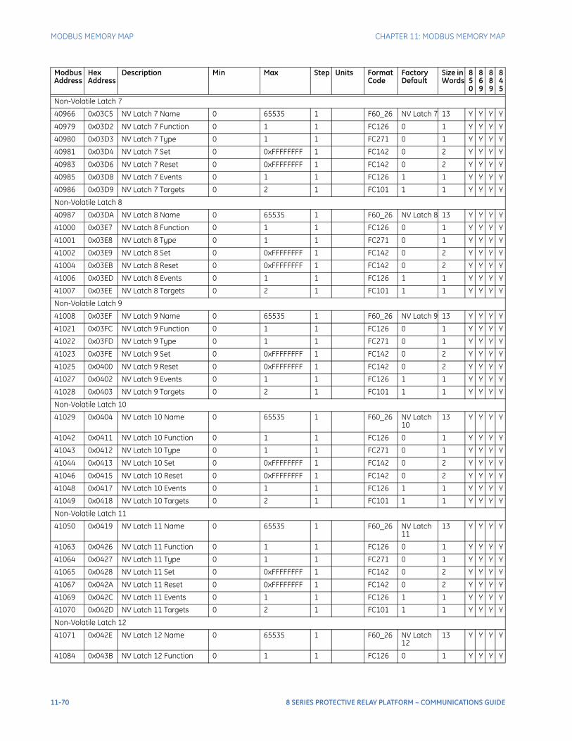
MODBUS MEMORY MAP CHAPTER 11: MODBUS MEMORY MAP
Non-Volatile Latch 7
40966 0x03C5 NV Latch 7 Name 0 65535 1 F60_26 NV Latch 7 13 Y Y Y Y
40979 0x03D2 NV Latch 7 Function 0 1 1 FC126 0 1 Y Y Y Y
40980 0x03D3 NV Latch 7 Type 0 1 1 FC271 0 1 Y Y Y Y
40981 0x03D4 NV Latch 7 Set 0 0xFFFFFFFF 1 FC142 0 2 Y Y Y Y
40983 0x03D6 NV Latch 7 Reset 0 0xFFFFFFFF 1 FC142 0 2 Y Y Y Y
40985 0x03D8 NV Latch 7 Events 0 1 1 FC126 1 1 Y Y Y Y
40986 0x03D9 NV Latch 7 Targets 0 2 1 FC101 1 1 Y Y Y Y
Non-Volatile Latch 8
40987 0x03DA NV Latch 8 Name 0 65535 1 F60_26 NV Latch 8 13 Y Y Y Y
41000 0x03E7 NV Latch 8 Function 0 1 1 FC126 0 1 Y Y Y Y
41001 0x03E8 NV Latch 8 Type 0 1 1 FC271 0 1 Y Y Y Y
41002 0x03E9 NV Latch 8 Set 0 0xFFFFFFFF 1 FC142 0 2 Y Y Y Y
41004 0x03EB NV Latch 8 Reset 0 0xFFFFFFFF 1 FC142 0 2 Y Y Y Y
41006 0x03ED NV Latch 8 Events 0 1 1 FC126 1 1 Y Y Y Y
41007 0x03EE NV Latch 8 Targets 0 2 1 FC101 1 1 Y Y Y Y
Non-Volatile Latch 9
41008 0x03EF NV Latch 9 Name 0 65535 1 F60_26 NV Latch 9 13 Y Y Y Y
41021 0x03FC NV Latch 9 Function 0 1 1 FC126 0 1 Y Y Y Y
41022 0x03FD NV Latch 9 Type 0 1 1 FC271 0 1 Y Y Y Y
41023 0x03FE NV Latch 9 Set 0 0xFFFFFFFF 1 FC142 0 2 Y Y Y Y
41025 0x0400 NV Latch 9 Reset 0 0xFFFFFFFF 1 FC142 0 2 Y Y Y Y
41027 0x0402 NV Latch 9 Events 0 1 1 FC126 1 1 Y Y Y Y
41028 0x0403 NV Latch 9 Targets 0 2 1 FC101 1 1 Y Y Y Y
Non-Volatile Latch 10
41029 0x0404 NV Latch 10 Name 0 65535 1 F60_26 NV Latch 10
13 Y Y Y Y
41042 0x0411 NV Latch 10 Function 0 1 1 FC126 0 1 Y Y Y Y
41043 0x0412 NV Latch 10 Type 0 1 1 FC271 0 1 Y Y Y Y
41044 0x0413 NV Latch 10 Set 0 0xFFFFFFFF 1 FC142 0 2 Y Y Y Y
41046 0x0415 NV Latch 10 Reset 0 0xFFFFFFFF 1 FC142 0 2 Y Y Y Y
41048 0x0417 NV Latch 10 Events 0 1 1 FC126 1 1 Y Y Y Y
41049 0x0418 NV Latch 10 Targets 0 2 1 FC101 1 1 Y Y Y Y
Non-Volatile Latch 11
41050 0x0419 NV Latch 11 Name 0 65535 1 F60_26 NV Latch 11
13 Y Y Y Y
41063 0x0426 NV Latch 11 Function 0 1 1 FC126 0 1 Y Y Y Y
41064 0x0427 NV Latch 11 Type 0 1 1 FC271 0 1 Y Y Y Y
41065 0x0428 NV Latch 11 Set 0 0xFFFFFFFF 1 FC142 0 2 Y Y Y Y
41067 0x042A NV Latch 11 Reset 0 0xFFFFFFFF 1 FC142 0 2 Y Y Y Y
41069 0x042C NV Latch 11 Events 0 1 1 FC126 1 1 Y Y Y Y
41070 0x042D NV Latch 11 Targets 0 2 1 FC101 1 1 Y Y Y Y
Non-Volatile Latch 12
41071 0x042E NV Latch 12 Name 0 65535 1 F60_26 NV Latch 12
13 Y Y Y Y
41084 0x043B NV Latch 12 Function 0 1 1 FC126 0 1 Y Y Y Y
Modbus Address
Hex Address
Description Min Max Step Units Format Code
Factory Default
Size in Words
850
869
889
845
11-70 8 SERIES PROTECTIVE RELAY PLATFORM – COMMUNICATIONS GUIDE
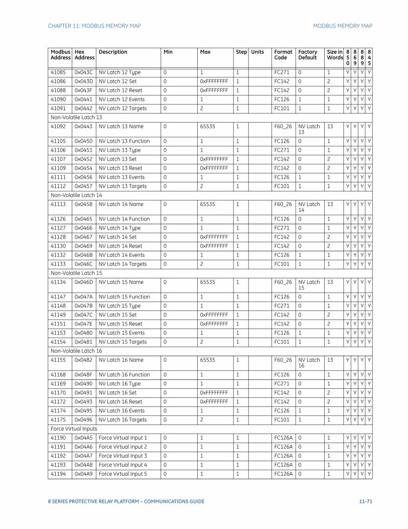
CHAPTER 11: MODBUS MEMORY MAP MODBUS MEMORY MAP
41085 0x043C NV Latch 12 Type 0 1 1 FC271 0 1 Y Y Y Y
41086 0x043D NV Latch 12 Set 0 0xFFFFFFFF 1 FC142 0 2 Y Y Y Y
41088 0x043F NV Latch 12 Reset 0 0xFFFFFFFF 1 FC142 0 2 Y Y Y Y
41090 0x0441 NV Latch 12 Events 0 1 1 FC126 1 1 Y Y Y Y
41091 0x0442 NV Latch 12 Targets 0 2 1 FC101 1 1 Y Y Y Y
Non-Volatile Latch 13
41092 0x0443 NV Latch 13 Name 0 65535 1 F60_26 NV Latch 13
13 Y Y Y Y
41105 0x0450 NV Latch 13 Function 0 1 1 FC126 0 1 Y Y Y Y
41106 0x0451 NV Latch 13 Type 0 1 1 FC271 0 1 Y Y Y Y
41107 0x0452 NV Latch 13 Set 0 0xFFFFFFFF 1 FC142 0 2 Y Y Y Y
41109 0x0454 NV Latch 13 Reset 0 0xFFFFFFFF 1 FC142 0 2 Y Y Y Y
41111 0x0456 NV Latch 13 Events 0 1 1 FC126 1 1 Y Y Y Y
41112 0x0457 NV Latch 13 Targets 0 2 1 FC101 1 1 Y Y Y Y
Non-Volatile Latch 14
41113 0x0458 NV Latch 14 Name 0 65535 1 F60_26 NV Latch 14
13 Y Y Y Y
41126 0x0465 NV Latch 14 Function 0 1 1 FC126 0 1 Y Y Y Y
41127 0x0466 NV Latch 14 Type 0 1 1 FC271 0 1 Y Y Y Y
41128 0x0467 NV Latch 14 Set 0 0xFFFFFFFF 1 FC142 0 2 Y Y Y Y
41130 0x0469 NV Latch 14 Reset 0 0xFFFFFFFF 1 FC142 0 2 Y Y Y Y
41132 0x046B NV Latch 14 Events 0 1 1 FC126 1 1 Y Y Y Y
41133 0x046C NV Latch 14 Targets 0 2 1 FC101 1 1 Y Y Y Y
Non-Volatile Latch 15
41134 0x046D NV Latch 15 Name 0 65535 1 F60_26 NV Latch 15
13 Y Y Y Y
41147 0x047A NV Latch 15 Function 0 1 1 FC126 0 1 Y Y Y Y
41148 0x047B NV Latch 15 Type 0 1 1 FC271 0 1 Y Y Y Y
41149 0x047C NV Latch 15 Set 0 0xFFFFFFFF 1 FC142 0 2 Y Y Y Y
41151 0x047E NV Latch 15 Reset 0 0xFFFFFFFF 1 FC142 0 2 Y Y Y Y
41153 0x0480 NV Latch 15 Events 0 1 1 FC126 1 1 Y Y Y Y
41154 0x0481 NV Latch 15 Targets 0 2 1 FC101 1 1 Y Y Y Y
Non-Volatile Latch 16
41155 0x0482 NV Latch 16 Name 0 65535 1 F60_26 NV Latch 16
13 Y Y Y Y
41168 0x048F NV Latch 16 Function 0 1 1 FC126 0 1 Y Y Y Y
41169 0x0490 NV Latch 16 Type 0 1 1 FC271 0 1 Y Y Y Y
41170 0x0491 NV Latch 16 Set 0 0xFFFFFFFF 1 FC142 0 2 Y Y Y Y
41172 0x0493 NV Latch 16 Reset 0 0xFFFFFFFF 1 FC142 0 2 Y Y Y Y
41174 0x0495 NV Latch 16 Events 0 1 1 FC126 1 1 Y Y Y Y
41175 0x0496 NV Latch 16 Targets 0 2 1 FC101 1 1 Y Y Y Y
Force Virtual Inputs
41190 0x04A5 Force Virtual Input 1 0 1 1 FC126A 0 1 Y Y Y Y
41191 0x04A6 Force Virtual Input 2 0 1 1 FC126A 0 1 Y Y Y Y
41192 0x04A7 Force Virtual Input 3 0 1 1 FC126A 0 1 Y Y Y Y
41193 0x04A8 Force Virtual Input 4 0 1 1 FC126A 0 1 Y Y Y Y
41194 0x04A9 Force Virtual Input 5 0 1 1 FC126A 0 1 Y Y Y Y
Modbus Address
Hex Address
Description Min Max Step Units Format Code
Factory Default
Size in Words
850
869
889
845
8 SERIES PROTECTIVE RELAY PLATFORM – COMMUNICATIONS GUIDE 11-71
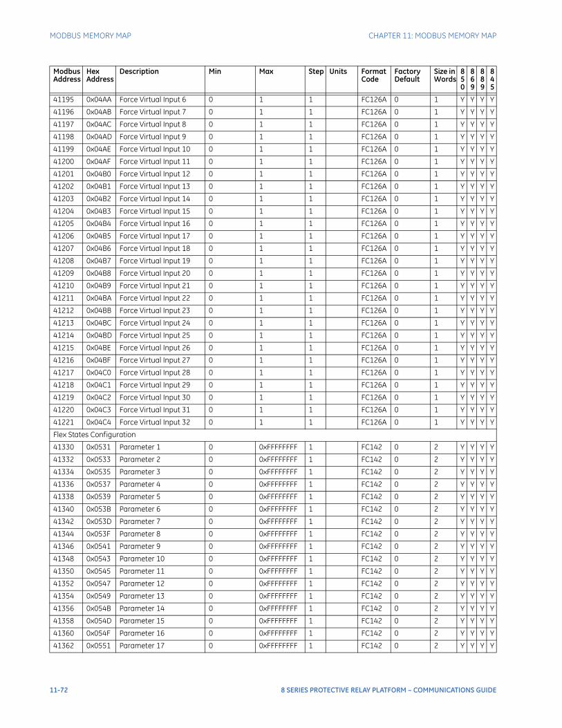
MODBUS MEMORY MAP CHAPTER 11: MODBUS MEMORY MAP
41195 0x04AA Force Virtual Input 6 0 1 1 FC126A 0 1 Y Y Y Y
41196 0x04AB Force Virtual Input 7 0 1 1 FC126A 0 1 Y Y Y Y
41197 0x04AC Force Virtual Input 8 0 1 1 FC126A 0 1 Y Y Y Y
41198 0x04AD Force Virtual Input 9 0 1 1 FC126A 0 1 Y Y Y Y
41199 0x04AE Force Virtual Input 10 0 1 1 FC126A 0 1 Y Y Y Y
41200 0x04AF Force Virtual Input 11 0 1 1 FC126A 0 1 Y Y Y Y
41201 0x04B0 Force Virtual Input 12 0 1 1 FC126A 0 1 Y Y Y Y
41202 0x04B1 Force Virtual Input 13 0 1 1 FC126A 0 1 Y Y Y Y
41203 0x04B2 Force Virtual Input 14 0 1 1 FC126A 0 1 Y Y Y Y
41204 0x04B3 Force Virtual Input 15 0 1 1 FC126A 0 1 Y Y Y Y
41205 0x04B4 Force Virtual Input 16 0 1 1 FC126A 0 1 Y Y Y Y
41206 0x04B5 Force Virtual Input 17 0 1 1 FC126A 0 1 Y Y Y Y
41207 0x04B6 Force Virtual Input 18 0 1 1 FC126A 0 1 Y Y Y Y
41208 0x04B7 Force Virtual Input 19 0 1 1 FC126A 0 1 Y Y Y Y
41209 0x04B8 Force Virtual Input 20 0 1 1 FC126A 0 1 Y Y Y Y
41210 0x04B9 Force Virtual Input 21 0 1 1 FC126A 0 1 Y Y Y Y
41211 0x04BA Force Virtual Input 22 0 1 1 FC126A 0 1 Y Y Y Y
41212 0x04BB Force Virtual Input 23 0 1 1 FC126A 0 1 Y Y Y Y
41213 0x04BC Force Virtual Input 24 0 1 1 FC126A 0 1 Y Y Y Y
41214 0x04BD Force Virtual Input 25 0 1 1 FC126A 0 1 Y Y Y Y
41215 0x04BE Force Virtual Input 26 0 1 1 FC126A 0 1 Y Y Y Y
41216 0x04BF Force Virtual Input 27 0 1 1 FC126A 0 1 Y Y Y Y
41217 0x04C0 Force Virtual Input 28 0 1 1 FC126A 0 1 Y Y Y Y
41218 0x04C1 Force Virtual Input 29 0 1 1 FC126A 0 1 Y Y Y Y
41219 0x04C2 Force Virtual Input 30 0 1 1 FC126A 0 1 Y Y Y Y
41220 0x04C3 Force Virtual Input 31 0 1 1 FC126A 0 1 Y Y Y Y
41221 0x04C4 Force Virtual Input 32 0 1 1 FC126A 0 1 Y Y Y Y
Flex States Configuration
41330 0x0531 Parameter 1 0 0xFFFFFFFF 1 FC142 0 2 Y Y Y Y
41332 0x0533 Parameter 2 0 0xFFFFFFFF 1 FC142 0 2 Y Y Y Y
41334 0x0535 Parameter 3 0 0xFFFFFFFF 1 FC142 0 2 Y Y Y Y
41336 0x0537 Parameter 4 0 0xFFFFFFFF 1 FC142 0 2 Y Y Y Y
41338 0x0539 Parameter 5 0 0xFFFFFFFF 1 FC142 0 2 Y Y Y Y
41340 0x053B Parameter 6 0 0xFFFFFFFF 1 FC142 0 2 Y Y Y Y
41342 0x053D Parameter 7 0 0xFFFFFFFF 1 FC142 0 2 Y Y Y Y
41344 0x053F Parameter 8 0 0xFFFFFFFF 1 FC142 0 2 Y Y Y Y
41346 0x0541 Parameter 9 0 0xFFFFFFFF 1 FC142 0 2 Y Y Y Y
41348 0x0543 Parameter 10 0 0xFFFFFFFF 1 FC142 0 2 Y Y Y Y
41350 0x0545 Parameter 11 0 0xFFFFFFFF 1 FC142 0 2 Y Y Y Y
41352 0x0547 Parameter 12 0 0xFFFFFFFF 1 FC142 0 2 Y Y Y Y
41354 0x0549 Parameter 13 0 0xFFFFFFFF 1 FC142 0 2 Y Y Y Y
41356 0x054B Parameter 14 0 0xFFFFFFFF 1 FC142 0 2 Y Y Y Y
41358 0x054D Parameter 15 0 0xFFFFFFFF 1 FC142 0 2 Y Y Y Y
41360 0x054F Parameter 16 0 0xFFFFFFFF 1 FC142 0 2 Y Y Y Y
41362 0x0551 Parameter 17 0 0xFFFFFFFF 1 FC142 0 2 Y Y Y Y
Modbus Address
Hex Address
Description Min Max Step Units Format Code
Factory Default
Size in Words
850
869
889
845
11-72 8 SERIES PROTECTIVE RELAY PLATFORM – COMMUNICATIONS GUIDE
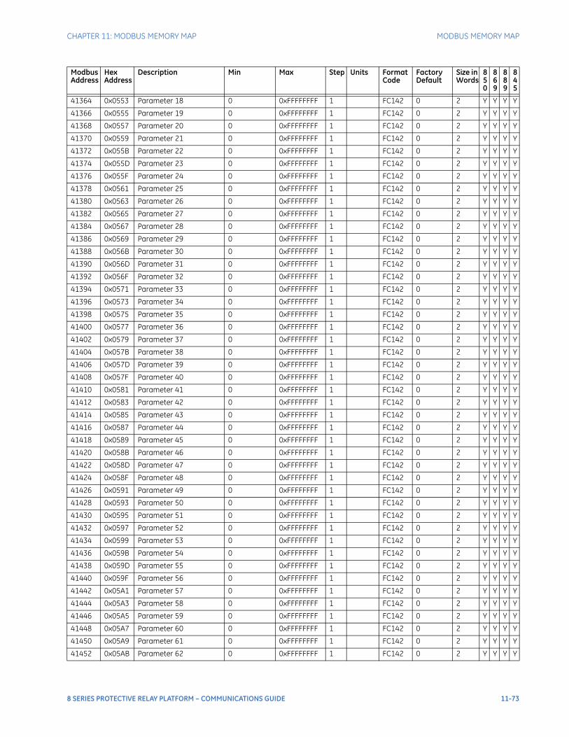
CHAPTER 11: MODBUS MEMORY MAP MODBUS MEMORY MAP
41364 0x0553 Parameter 18 0 0xFFFFFFFF 1 FC142 0 2 Y Y Y Y
41366 0x0555 Parameter 19 0 0xFFFFFFFF 1 FC142 0 2 Y Y Y Y
41368 0x0557 Parameter 20 0 0xFFFFFFFF 1 FC142 0 2 Y Y Y Y
41370 0x0559 Parameter 21 0 0xFFFFFFFF 1 FC142 0 2 Y Y Y Y
41372 0x055B Parameter 22 0 0xFFFFFFFF 1 FC142 0 2 Y Y Y Y
41374 0x055D Parameter 23 0 0xFFFFFFFF 1 FC142 0 2 Y Y Y Y
41376 0x055F Parameter 24 0 0xFFFFFFFF 1 FC142 0 2 Y Y Y Y
41378 0x0561 Parameter 25 0 0xFFFFFFFF 1 FC142 0 2 Y Y Y Y
41380 0x0563 Parameter 26 0 0xFFFFFFFF 1 FC142 0 2 Y Y Y Y
41382 0x0565 Parameter 27 0 0xFFFFFFFF 1 FC142 0 2 Y Y Y Y
41384 0x0567 Parameter 28 0 0xFFFFFFFF 1 FC142 0 2 Y Y Y Y
41386 0x0569 Parameter 29 0 0xFFFFFFFF 1 FC142 0 2 Y Y Y Y
41388 0x056B Parameter 30 0 0xFFFFFFFF 1 FC142 0 2 Y Y Y Y
41390 0x056D Parameter 31 0 0xFFFFFFFF 1 FC142 0 2 Y Y Y Y
41392 0x056F Parameter 32 0 0xFFFFFFFF 1 FC142 0 2 Y Y Y Y
41394 0x0571 Parameter 33 0 0xFFFFFFFF 1 FC142 0 2 Y Y Y Y
41396 0x0573 Parameter 34 0 0xFFFFFFFF 1 FC142 0 2 Y Y Y Y
41398 0x0575 Parameter 35 0 0xFFFFFFFF 1 FC142 0 2 Y Y Y Y
41400 0x0577 Parameter 36 0 0xFFFFFFFF 1 FC142 0 2 Y Y Y Y
41402 0x0579 Parameter 37 0 0xFFFFFFFF 1 FC142 0 2 Y Y Y Y
41404 0x057B Parameter 38 0 0xFFFFFFFF 1 FC142 0 2 Y Y Y Y
41406 0x057D Parameter 39 0 0xFFFFFFFF 1 FC142 0 2 Y Y Y Y
41408 0x057F Parameter 40 0 0xFFFFFFFF 1 FC142 0 2 Y Y Y Y
41410 0x0581 Parameter 41 0 0xFFFFFFFF 1 FC142 0 2 Y Y Y Y
41412 0x0583 Parameter 42 0 0xFFFFFFFF 1 FC142 0 2 Y Y Y Y
41414 0x0585 Parameter 43 0 0xFFFFFFFF 1 FC142 0 2 Y Y Y Y
41416 0x0587 Parameter 44 0 0xFFFFFFFF 1 FC142 0 2 Y Y Y Y
41418 0x0589 Parameter 45 0 0xFFFFFFFF 1 FC142 0 2 Y Y Y Y
41420 0x058B Parameter 46 0 0xFFFFFFFF 1 FC142 0 2 Y Y Y Y
41422 0x058D Parameter 47 0 0xFFFFFFFF 1 FC142 0 2 Y Y Y Y
41424 0x058F Parameter 48 0 0xFFFFFFFF 1 FC142 0 2 Y Y Y Y
41426 0x0591 Parameter 49 0 0xFFFFFFFF 1 FC142 0 2 Y Y Y Y
41428 0x0593 Parameter 50 0 0xFFFFFFFF 1 FC142 0 2 Y Y Y Y
41430 0x0595 Parameter 51 0 0xFFFFFFFF 1 FC142 0 2 Y Y Y Y
41432 0x0597 Parameter 52 0 0xFFFFFFFF 1 FC142 0 2 Y Y Y Y
41434 0x0599 Parameter 53 0 0xFFFFFFFF 1 FC142 0 2 Y Y Y Y
41436 0x059B Parameter 54 0 0xFFFFFFFF 1 FC142 0 2 Y Y Y Y
41438 0x059D Parameter 55 0 0xFFFFFFFF 1 FC142 0 2 Y Y Y Y
41440 0x059F Parameter 56 0 0xFFFFFFFF 1 FC142 0 2 Y Y Y Y
41442 0x05A1 Parameter 57 0 0xFFFFFFFF 1 FC142 0 2 Y Y Y Y
41444 0x05A3 Parameter 58 0 0xFFFFFFFF 1 FC142 0 2 Y Y Y Y
41446 0x05A5 Parameter 59 0 0xFFFFFFFF 1 FC142 0 2 Y Y Y Y
41448 0x05A7 Parameter 60 0 0xFFFFFFFF 1 FC142 0 2 Y Y Y Y
41450 0x05A9 Parameter 61 0 0xFFFFFFFF 1 FC142 0 2 Y Y Y Y
41452 0x05AB Parameter 62 0 0xFFFFFFFF 1 FC142 0 2 Y Y Y Y
Modbus Address
Hex Address
Description Min Max Step Units Format Code
Factory Default
Size in Words
850
869
889
845
8 SERIES PROTECTIVE RELAY PLATFORM – COMMUNICATIONS GUIDE 11-73
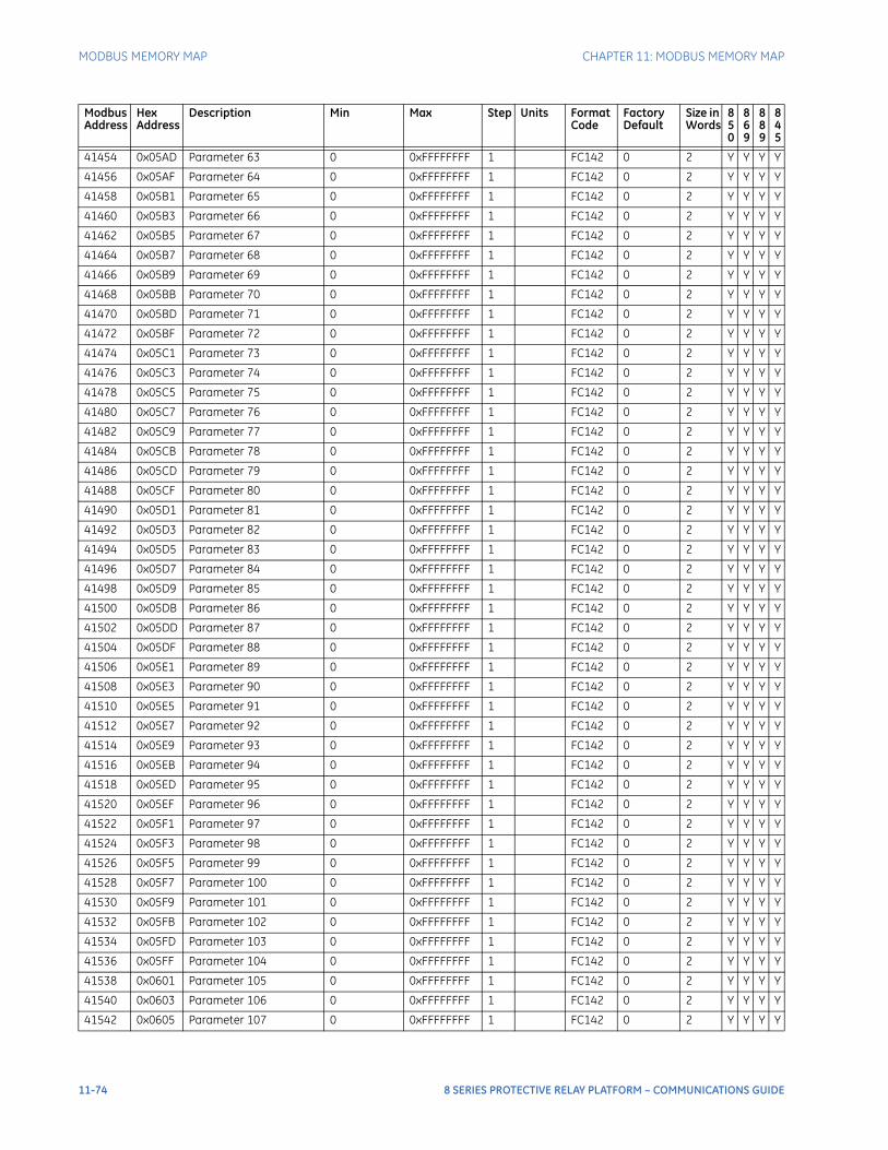
MODBUS MEMORY MAP CHAPTER 11: MODBUS MEMORY MAP
41454 0x05AD Parameter 63 0 0xFFFFFFFF 1 FC142 0 2 Y Y Y Y
41456 0x05AF Parameter 64 0 0xFFFFFFFF 1 FC142 0 2 Y Y Y Y
41458 0x05B1 Parameter 65 0 0xFFFFFFFF 1 FC142 0 2 Y Y Y Y
41460 0x05B3 Parameter 66 0 0xFFFFFFFF 1 FC142 0 2 Y Y Y Y
41462 0x05B5 Parameter 67 0 0xFFFFFFFF 1 FC142 0 2 Y Y Y Y
41464 0x05B7 Parameter 68 0 0xFFFFFFFF 1 FC142 0 2 Y Y Y Y
41466 0x05B9 Parameter 69 0 0xFFFFFFFF 1 FC142 0 2 Y Y Y Y
41468 0x05BB Parameter 70 0 0xFFFFFFFF 1 FC142 0 2 Y Y Y Y
41470 0x05BD Parameter 71 0 0xFFFFFFFF 1 FC142 0 2 Y Y Y Y
41472 0x05BF Parameter 72 0 0xFFFFFFFF 1 FC142 0 2 Y Y Y Y
41474 0x05C1 Parameter 73 0 0xFFFFFFFF 1 FC142 0 2 Y Y Y Y
41476 0x05C3 Parameter 74 0 0xFFFFFFFF 1 FC142 0 2 Y Y Y Y
41478 0x05C5 Parameter 75 0 0xFFFFFFFF 1 FC142 0 2 Y Y Y Y
41480 0x05C7 Parameter 76 0 0xFFFFFFFF 1 FC142 0 2 Y Y Y Y
41482 0x05C9 Parameter 77 0 0xFFFFFFFF 1 FC142 0 2 Y Y Y Y
41484 0x05CB Parameter 78 0 0xFFFFFFFF 1 FC142 0 2 Y Y Y Y
41486 0x05CD Parameter 79 0 0xFFFFFFFF 1 FC142 0 2 Y Y Y Y
41488 0x05CF Parameter 80 0 0xFFFFFFFF 1 FC142 0 2 Y Y Y Y
41490 0x05D1 Parameter 81 0 0xFFFFFFFF 1 FC142 0 2 Y Y Y Y
41492 0x05D3 Parameter 82 0 0xFFFFFFFF 1 FC142 0 2 Y Y Y Y
41494 0x05D5 Parameter 83 0 0xFFFFFFFF 1 FC142 0 2 Y Y Y Y
41496 0x05D7 Parameter 84 0 0xFFFFFFFF 1 FC142 0 2 Y Y Y Y
41498 0x05D9 Parameter 85 0 0xFFFFFFFF 1 FC142 0 2 Y Y Y Y
41500 0x05DB Parameter 86 0 0xFFFFFFFF 1 FC142 0 2 Y Y Y Y
41502 0x05DD Parameter 87 0 0xFFFFFFFF 1 FC142 0 2 Y Y Y Y
41504 0x05DF Parameter 88 0 0xFFFFFFFF 1 FC142 0 2 Y Y Y Y
41506 0x05E1 Parameter 89 0 0xFFFFFFFF 1 FC142 0 2 Y Y Y Y
41508 0x05E3 Parameter 90 0 0xFFFFFFFF 1 FC142 0 2 Y Y Y Y
41510 0x05E5 Parameter 91 0 0xFFFFFFFF 1 FC142 0 2 Y Y Y Y
41512 0x05E7 Parameter 92 0 0xFFFFFFFF 1 FC142 0 2 Y Y Y Y
41514 0x05E9 Parameter 93 0 0xFFFFFFFF 1 FC142 0 2 Y Y Y Y
41516 0x05EB Parameter 94 0 0xFFFFFFFF 1 FC142 0 2 Y Y Y Y
41518 0x05ED Parameter 95 0 0xFFFFFFFF 1 FC142 0 2 Y Y Y Y
41520 0x05EF Parameter 96 0 0xFFFFFFFF 1 FC142 0 2 Y Y Y Y
41522 0x05F1 Parameter 97 0 0xFFFFFFFF 1 FC142 0 2 Y Y Y Y
41524 0x05F3 Parameter 98 0 0xFFFFFFFF 1 FC142 0 2 Y Y Y Y
41526 0x05F5 Parameter 99 0 0xFFFFFFFF 1 FC142 0 2 Y Y Y Y
41528 0x05F7 Parameter 100 0 0xFFFFFFFF 1 FC142 0 2 Y Y Y Y
41530 0x05F9 Parameter 101 0 0xFFFFFFFF 1 FC142 0 2 Y Y Y Y
41532 0x05FB Parameter 102 0 0xFFFFFFFF 1 FC142 0 2 Y Y Y Y
41534 0x05FD Parameter 103 0 0xFFFFFFFF 1 FC142 0 2 Y Y Y Y
41536 0x05FF Parameter 104 0 0xFFFFFFFF 1 FC142 0 2 Y Y Y Y
41538 0x0601 Parameter 105 0 0xFFFFFFFF 1 FC142 0 2 Y Y Y Y
41540 0x0603 Parameter 106 0 0xFFFFFFFF 1 FC142 0 2 Y Y Y Y
41542 0x0605 Parameter 107 0 0xFFFFFFFF 1 FC142 0 2 Y Y Y Y
Modbus Address
Hex Address
Description Min Max Step Units Format Code
Factory Default
Size in Words
850
869
889
845
11-74 8 SERIES PROTECTIVE RELAY PLATFORM – COMMUNICATIONS GUIDE

CHAPTER 11: MODBUS MEMORY MAP MODBUS MEMORY MAP
41544 0x0607 Parameter 108 0 0xFFFFFFFF 1 FC142 0 2 Y Y Y Y
41546 0x0609 Parameter 109 0 0xFFFFFFFF 1 FC142 0 2 Y Y Y Y
41548 0x060B Parameter 110 0 0xFFFFFFFF 1 FC142 0 2 Y Y Y Y
41550 0x060D Parameter 111 0 0xFFFFFFFF 1 FC142 0 2 Y Y Y Y
41552 0x060F Parameter 112 0 0xFFFFFFFF 1 FC142 0 2 Y Y Y Y
41554 0x0611 Parameter 113 0 0xFFFFFFFF 1 FC142 0 2 Y Y Y Y
41556 0x0613 Parameter 114 0 0xFFFFFFFF 1 FC142 0 2 Y Y Y Y
41558 0x0615 Parameter 115 0 0xFFFFFFFF 1 FC142 0 2 Y Y Y Y
41560 0x0617 Parameter 116 0 0xFFFFFFFF 1 FC142 0 2 Y Y Y Y
41562 0x0619 Parameter 117 0 0xFFFFFFFF 1 FC142 0 2 Y Y Y Y
41564 0x061B Parameter 118 0 0xFFFFFFFF 1 FC142 0 2 Y Y Y Y
41566 0x061D Parameter 119 0 0xFFFFFFFF 1 FC142 0 2 Y Y Y Y
41568 0x061F Parameter 120 0 0xFFFFFFFF 1 FC142 0 2 Y Y Y Y
41570 0x0621 Parameter 121 0 0xFFFFFFFF 1 FC142 0 2 Y Y Y Y
41572 0x0623 Parameter 122 0 0xFFFFFFFF 1 FC142 0 2 Y Y Y Y
41574 0x0625 Parameter 123 0 0xFFFFFFFF 1 FC142 0 2 Y Y Y Y
41576 0x0627 Parameter 124 0 0xFFFFFFFF 1 FC142 0 2 Y Y Y Y
41578 0x0629 Parameter 125 0 0xFFFFFFFF 1 FC142 0 2 Y Y Y Y
41580 0x062B Parameter 126 0 0xFFFFFFFF 1 FC142 0 2 Y Y Y Y
41582 0x062D Parameter 127 0 0xFFFFFFFF 1 FC142 0 2 Y Y Y Y
41584 0x062F Parameter 128 0 0xFFFFFFFF 1 FC142 0 2 Y Y Y Y
41586 0x0631 Parameter 129 0 0xFFFFFFFF 1 FC142 0 2 Y Y Y Y
41588 0x0633 Parameter 130 0 0xFFFFFFFF 1 FC142 0 2 Y Y Y Y
41590 0x0635 Parameter 131 0 0xFFFFFFFF 1 FC142 0 2 Y Y Y Y
41592 0x0637 Parameter 132 0 0xFFFFFFFF 1 FC142 0 2 Y Y Y Y
41594 0x0639 Parameter 133 0 0xFFFFFFFF 1 FC142 0 2 Y Y Y Y
41596 0x063B Parameter 134 0 0xFFFFFFFF 1 FC142 0 2 Y Y Y Y
41598 0x063D Parameter 135 0 0xFFFFFFFF 1 FC142 0 2 Y Y Y Y
41600 0x063F Parameter 136 0 0xFFFFFFFF 1 FC142 0 2 Y Y Y Y
41602 0x0641 Parameter 137 0 0xFFFFFFFF 1 FC142 0 2 Y Y Y Y
41604 0x0643 Parameter 138 0 0xFFFFFFFF 1 FC142 0 2 Y Y Y Y
41606 0x0645 Parameter 139 0 0xFFFFFFFF 1 FC142 0 2 Y Y Y Y
41608 0x0647 Parameter 140 0 0xFFFFFFFF 1 FC142 0 2 Y Y Y Y
41610 0x0649 Parameter 141 0 0xFFFFFFFF 1 FC142 0 2 Y Y Y Y
41612 0x064B Parameter 142 0 0xFFFFFFFF 1 FC142 0 2 Y Y Y Y
41614 0x064D Parameter 143 0 0xFFFFFFFF 1 FC142 0 2 Y Y Y Y
41616 0x064F Parameter 144 0 0xFFFFFFFF 1 FC142 0 2 Y Y Y Y
41618 0x0651 Parameter 145 0 0xFFFFFFFF 1 FC142 0 2 Y Y Y Y
41620 0x0653 Parameter 146 0 0xFFFFFFFF 1 FC142 0 2 Y Y Y Y
41622 0x0655 Parameter 147 0 0xFFFFFFFF 1 FC142 0 2 Y Y Y Y
41624 0x0657 Parameter 148 0 0xFFFFFFFF 1 FC142 0 2 Y Y Y Y
41626 0x0659 Parameter 149 0 0xFFFFFFFF 1 FC142 0 2 Y Y Y Y
41628 0x065B Parameter 150 0 0xFFFFFFFF 1 FC142 0 2 Y Y Y Y
41630 0x065D Parameter 151 0 0xFFFFFFFF 1 FC142 0 2 Y Y Y Y
41632 0x065F Parameter 152 0 0xFFFFFFFF 1 FC142 0 2 Y Y Y Y
Modbus Address
Hex Address
Description Min Max Step Units Format Code
Factory Default
Size in Words
850
869
889
845
8 SERIES PROTECTIVE RELAY PLATFORM – COMMUNICATIONS GUIDE 11-75

MODBUS MEMORY MAP CHAPTER 11: MODBUS MEMORY MAP
41634 0x0661 Parameter 153 0 0xFFFFFFFF 1 FC142 0 2 Y Y Y Y
41636 0x0663 Parameter 154 0 0xFFFFFFFF 1 FC142 0 2 Y Y Y Y
41638 0x0665 Parameter 155 0 0xFFFFFFFF 1 FC142 0 2 Y Y Y Y
41640 0x0667 Parameter 156 0 0xFFFFFFFF 1 FC142 0 2 Y Y Y Y
41642 0x0669 Parameter 157 0 0xFFFFFFFF 1 FC142 0 2 Y Y Y Y
41644 0x066B Parameter 158 0 0xFFFFFFFF 1 FC142 0 2 Y Y Y Y
41646 0x066D Parameter 159 0 0xFFFFFFFF 1 FC142 0 2 Y Y Y Y
41648 0x066F Parameter 160 0 0xFFFFFFFF 1 FC142 0 2 Y Y Y Y
41650 0x0671 Parameter 161 0 0xFFFFFFFF 1 FC142 0 2 Y Y Y Y
41652 0x0673 Parameter 162 0 0xFFFFFFFF 1 FC142 0 2 Y Y Y Y
41654 0x0675 Parameter 163 0 0xFFFFFFFF 1 FC142 0 2 Y Y Y Y
41656 0x0677 Parameter 164 0 0xFFFFFFFF 1 FC142 0 2 Y Y Y Y
41658 0x0679 Parameter 165 0 0xFFFFFFFF 1 FC142 0 2 Y Y Y Y
41660 0x067B Parameter 166 0 0xFFFFFFFF 1 FC142 0 2 Y Y Y Y
41662 0x067D Parameter 167 0 0xFFFFFFFF 1 FC142 0 2 Y Y Y Y
41664 0x067F Parameter 168 0 0xFFFFFFFF 1 FC142 0 2 Y Y Y Y
41666 0x0681 Parameter 169 0 0xFFFFFFFF 1 FC142 0 2 Y Y Y Y
41668 0x0683 Parameter 170 0 0xFFFFFFFF 1 FC142 0 2 Y Y Y Y
41670 0x0685 Parameter 171 0 0xFFFFFFFF 1 FC142 0 2 Y Y Y Y
41672 0x0687 Parameter 172 0 0xFFFFFFFF 1 FC142 0 2 Y Y Y Y
41674 0x0689 Parameter 173 0 0xFFFFFFFF 1 FC142 0 2 Y Y Y Y
41676 0x068B Parameter 174 0 0xFFFFFFFF 1 FC142 0 2 Y Y Y Y
41678 0x068D Parameter 175 0 0xFFFFFFFF 1 FC142 0 2 Y Y Y Y
41680 0x068F Parameter 176 0 0xFFFFFFFF 1 FC142 0 2 Y Y Y Y
41682 0x0691 Parameter 177 0 0xFFFFFFFF 1 FC142 0 2 Y Y Y Y
41684 0x0693 Parameter 178 0 0xFFFFFFFF 1 FC142 0 2 Y Y Y Y
41686 0x0695 Parameter 179 0 0xFFFFFFFF 1 FC142 0 2 Y Y Y Y
41688 0x0697 Parameter 180 0 0xFFFFFFFF 1 FC142 0 2 Y Y Y Y
41690 0x0699 Parameter 181 0 0xFFFFFFFF 1 FC142 0 2 Y Y Y Y
41692 0x069B Parameter 182 0 0xFFFFFFFF 1 FC142 0 2 Y Y Y Y
41694 0x069D Parameter 183 0 0xFFFFFFFF 1 FC142 0 2 Y Y Y Y
41696 0x069F Parameter 184 0 0xFFFFFFFF 1 FC142 0 2 Y Y Y Y
41698 0x06A1 Parameter 185 0 0xFFFFFFFF 1 FC142 0 2 Y Y Y Y
41700 0x06A3 Parameter 186 0 0xFFFFFFFF 1 FC142 0 2 Y Y Y Y
41702 0x06A5 Parameter 187 0 0xFFFFFFFF 1 FC142 0 2 Y Y Y Y
41704 0x06A7 Parameter 188 0 0xFFFFFFFF 1 FC142 0 2 Y Y Y Y
41706 0x06A9 Parameter 189 0 0xFFFFFFFF 1 FC142 0 2 Y Y Y Y
41708 0x06AB Parameter 190 0 0xFFFFFFFF 1 FC142 0 2 Y Y Y Y
41710 0x06AD Parameter 191 0 0xFFFFFFFF 1 FC142 0 2 Y Y Y Y
41712 0x06AF Parameter 192 0 0xFFFFFFFF 1 FC142 0 2 Y Y Y Y
41714 0x06B1 Parameter 193 0 0xFFFFFFFF 1 FC142 0 2 Y Y Y Y
41716 0x06B3 Parameter 194 0 0xFFFFFFFF 1 FC142 0 2 Y Y Y Y
41718 0x06B5 Parameter 195 0 0xFFFFFFFF 1 FC142 0 2 Y Y Y Y
41720 0x06B7 Parameter 196 0 0xFFFFFFFF 1 FC142 0 2 Y Y Y Y
41722 0x06B9 Parameter 197 0 0xFFFFFFFF 1 FC142 0 2 Y Y Y Y
Modbus Address
Hex Address
Description Min Max Step Units Format Code
Factory Default
Size in Words
850
869
889
845
11-76 8 SERIES PROTECTIVE RELAY PLATFORM – COMMUNICATIONS GUIDE
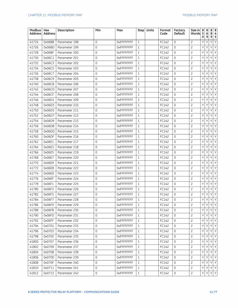
CHAPTER 11: MODBUS MEMORY MAP MODBUS MEMORY MAP
41724 0x06BB Parameter 198 0 0xFFFFFFFF 1 FC142 0 2 Y Y Y Y
41726 0x06BD Parameter 199 0 0xFFFFFFFF 1 FC142 0 2 Y Y Y Y
41728 0x06BF Parameter 200 0 0xFFFFFFFF 1 FC142 0 2 Y Y Y Y
41730 0x06C1 Parameter 201 0 0xFFFFFFFF 1 FC142 0 2 Y Y Y Y
41732 0x06C3 Parameter 202 0 0xFFFFFFFF 1 FC142 0 2 Y Y Y Y
41734 0x06C5 Parameter 203 0 0xFFFFFFFF 1 FC142 0 2 Y Y Y Y
41736 0x06C7 Parameter 204 0 0xFFFFFFFF 1 FC142 0 2 Y Y Y Y
41738 0x06C9 Parameter 205 0 0xFFFFFFFF 1 FC142 0 2 Y Y Y Y
41740 0x06CB Parameter 206 0 0xFFFFFFFF 1 FC142 0 2 Y Y Y Y
41742 0x06CD Parameter 207 0 0xFFFFFFFF 1 FC142 0 2 Y Y Y Y
41744 0x06CF Parameter 208 0 0xFFFFFFFF 1 FC142 0 2 Y Y Y Y
41746 0x06D1 Parameter 209 0 0xFFFFFFFF 1 FC142 0 2 Y Y Y Y
41748 0x06D3 Parameter 210 0 0xFFFFFFFF 1 FC142 0 2 Y Y Y Y
41750 0x06D5 Parameter 211 0 0xFFFFFFFF 1 FC142 0 2 Y Y Y Y
41752 0x06D7 Parameter 212 0 0xFFFFFFFF 1 FC142 0 2 Y Y Y Y
41754 0x06D9 Parameter 213 0 0xFFFFFFFF 1 FC142 0 2 Y Y Y Y
41756 0x06DB Parameter 214 0 0xFFFFFFFF 1 FC142 0 2 Y Y Y Y
41758 0x06DD Parameter 215 0 0xFFFFFFFF 1 FC142 0 2 Y Y Y Y
41760 0x06DF Parameter 216 0 0xFFFFFFFF 1 FC142 0 2 Y Y Y Y
41762 0x06E1 Parameter 217 0 0xFFFFFFFF 1 FC142 0 2 Y Y Y Y
41764 0x06E3 Parameter 218 0 0xFFFFFFFF 1 FC142 0 2 Y Y Y Y
41766 0x06E5 Parameter 219 0 0xFFFFFFFF 1 FC142 0 2 Y Y Y Y
41768 0x06E7 Parameter 220 0 0xFFFFFFFF 1 FC142 0 2 Y Y Y Y
41770 0x06E9 Parameter 221 0 0xFFFFFFFF 1 FC142 0 2 Y Y Y Y
41772 0x06EB Parameter 222 0 0xFFFFFFFF 1 FC142 0 2 Y Y Y Y
41774 0x06ED Parameter 223 0 0xFFFFFFFF 1 FC142 0 2 Y Y Y Y
41776 0x06EF Parameter 224 0 0xFFFFFFFF 1 FC142 0 2 Y Y Y Y
41778 0x06F1 Parameter 225 0 0xFFFFFFFF 1 FC142 0 2 Y Y Y Y
41780 0x06F3 Parameter 226 0 0xFFFFFFFF 1 FC142 0 2 Y Y Y Y
41782 0x06F5 Parameter 227 0 0xFFFFFFFF 1 FC142 0 2 Y Y Y Y
41784 0x06F7 Parameter 228 0 0xFFFFFFFF 1 FC142 0 2 Y Y Y Y
41786 0x06F9 Parameter 229 0 0xFFFFFFFF 1 FC142 0 2 Y Y Y Y
41788 0x06FB Parameter 230 0 0xFFFFFFFF 1 FC142 0 2 Y Y Y Y
41790 0x06FD Parameter 231 0 0xFFFFFFFF 1 FC142 0 2 Y Y Y Y
41792 0x06FF Parameter 232 0 0xFFFFFFFF 1 FC142 0 2 Y Y Y Y
41794 0x0701 Parameter 233 0 0xFFFFFFFF 1 FC142 0 2 Y Y Y Y
41796 0x0703 Parameter 234 0 0xFFFFFFFF 1 FC142 0 2 Y Y Y Y
41798 0x0705 Parameter 235 0 0xFFFFFFFF 1 FC142 0 2 Y Y Y Y
41800 0x0707 Parameter 236 0 0xFFFFFFFF 1 FC142 0 2 Y Y Y Y
41802 0x0709 Parameter 237 0 0xFFFFFFFF 1 FC142 0 2 Y Y Y Y
41804 0x070B Parameter 238 0 0xFFFFFFFF 1 FC142 0 2 Y Y Y Y
41806 0x070D Parameter 239 0 0xFFFFFFFF 1 FC142 0 2 Y Y Y Y
41808 0x070F Parameter 240 0 0xFFFFFFFF 1 FC142 0 2 Y Y Y Y
41810 0x0711 Parameter 241 0 0xFFFFFFFF 1 FC142 0 2 Y Y Y Y
41812 0x0713 Parameter 242 0 0xFFFFFFFF 1 FC142 0 2 Y Y Y Y
Modbus Address
Hex Address
Description Min Max Step Units Format Code
Factory Default
Size in Words
850
869
889
845
8 SERIES PROTECTIVE RELAY PLATFORM – COMMUNICATIONS GUIDE 11-77
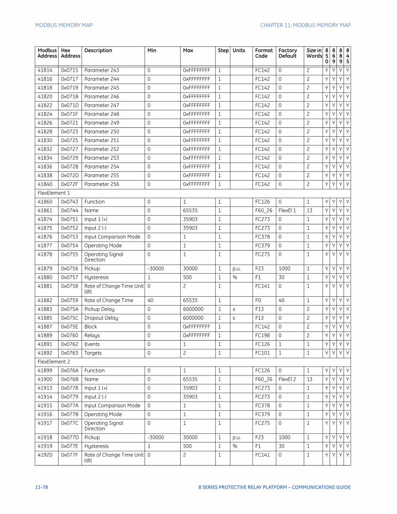
MODBUS MEMORY MAP CHAPTER 11: MODBUS MEMORY MAP
41814 0x0715 Parameter 243 0 0xFFFFFFFF 1 FC142 0 2 Y Y Y Y
41816 0x0717 Parameter 244 0 0xFFFFFFFF 1 FC142 0 2 Y Y Y Y
41818 0x0719 Parameter 245 0 0xFFFFFFFF 1 FC142 0 2 Y Y Y Y
41820 0x071B Parameter 246 0 0xFFFFFFFF 1 FC142 0 2 Y Y Y Y
41822 0x071D Parameter 247 0 0xFFFFFFFF 1 FC142 0 2 Y Y Y Y
41824 0x071F Parameter 248 0 0xFFFFFFFF 1 FC142 0 2 Y Y Y Y
41826 0x0721 Parameter 249 0 0xFFFFFFFF 1 FC142 0 2 Y Y Y Y
41828 0x0723 Parameter 250 0 0xFFFFFFFF 1 FC142 0 2 Y Y Y Y
41830 0x0725 Parameter 251 0 0xFFFFFFFF 1 FC142 0 2 Y Y Y Y
41832 0x0727 Parameter 252 0 0xFFFFFFFF 1 FC142 0 2 Y Y Y Y
41834 0x0729 Parameter 253 0 0xFFFFFFFF 1 FC142 0 2 Y Y Y Y
41836 0x072B Parameter 254 0 0xFFFFFFFF 1 FC142 0 2 Y Y Y Y
41838 0x072D Parameter 255 0 0xFFFFFFFF 1 FC142 0 2 Y Y Y Y
41840 0x072F Parameter 256 0 0xFFFFFFFF 1 FC142 0 2 Y Y Y Y
FlexElement 1
41860 0x0743 Function 0 1 1 FC126 0 1 Y Y Y Y
41861 0x0744 Name 0 65535 1 F60_26 FlexEl 1 13 Y Y Y Y
41874 0x0751 Input 1 (+) 0 35903 1 FC273 0 1 Y Y Y Y
41875 0x0752 Input 2 (-) 0 35903 1 FC273 0 1 Y Y Y Y
41876 0x0753 Input Comparison Mode 0 1 1 FC378 0 1 Y Y Y Y
41877 0x0754 Operating Mode 0 1 1 FC379 0 1 Y Y Y Y
41878 0x0755 Operating Signal Direction
0 1 1 FC275 0 1 Y Y Y Y
41879 0x0756 Pickup -30000 30000 1 p.u. F23 1000 1 Y Y Y Y
41880 0x0757 Hysteresis 1 500 1 % F1 30 1 Y Y Y Y
41881 0x0758 Rate of Change Time Unit (dt)
0 2 1 FC141 0 1 Y Y Y Y
41882 0x0759 Rate of Change Time 40 65535 1 F0 40 1 Y Y Y Y
41883 0x075A Pickup Delay 0 6000000 1 s F13 0 2 Y Y Y Y
41885 0x075C Dropout Delay 0 6000000 1 s F13 0 2 Y Y Y Y
41887 0x075E Block 0 0xFFFFFFFF 1 FC142 0 2 Y Y Y Y
41889 0x0760 Relays 0 0xFFFFFFFF 1 FC198 0 2 Y Y Y Y
41891 0x0762 Events 0 1 1 FC126 1 1 Y Y Y Y
41892 0x0763 Targets 0 2 1 FC101 1 1 Y Y Y Y
FlexElement 2
41899 0x076A Function 0 1 1 FC126 0 1 Y Y Y Y
41900 0x076B Name 0 65535 1 F60_26 FlexEl 2 13 Y Y Y Y
41913 0x0778 Input 1 (+) 0 35903 1 FC273 0 1 Y Y Y Y
41914 0x0779 Input 2 (-) 0 35903 1 FC273 0 1 Y Y Y Y
41915 0x077A Input Comparison Mode 0 1 1 FC378 0 1 Y Y Y Y
41916 0x077B Operating Mode 0 1 1 FC379 0 1 Y Y Y Y
41917 0x077C Operating Signal Direction
0 1 1 FC275 0 1 Y Y Y Y
41918 0x077D Pickup -30000 30000 1 p.u. F23 1000 1 Y Y Y Y
41919 0x077E Hysteresis 1 500 1 % F1 30 1 Y Y Y Y
41920 0x077F Rate of Change Time Unit (dt)
0 2 1 FC141 0 1 Y Y Y Y
Modbus Address
Hex Address
Description Min Max Step Units Format Code
Factory Default
Size in Words
850
869
889
845
11-78 8 SERIES PROTECTIVE RELAY PLATFORM – COMMUNICATIONS GUIDE
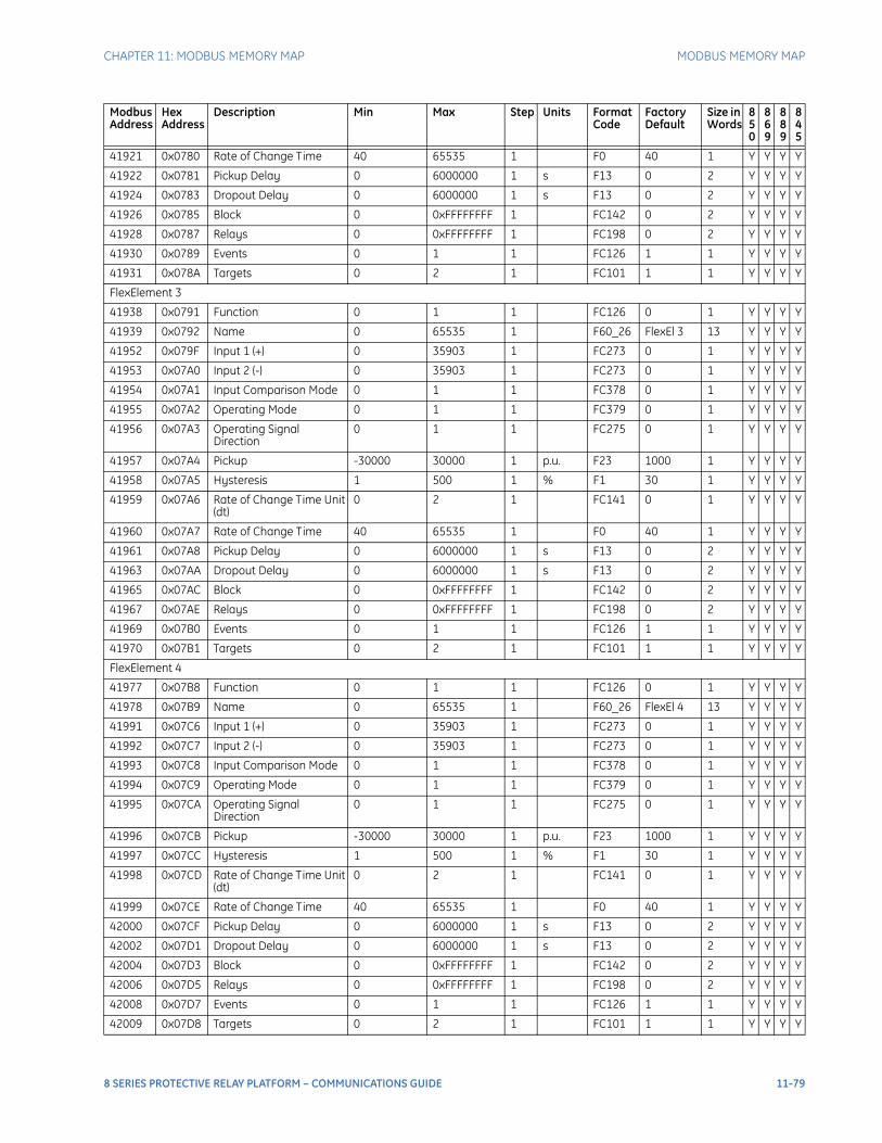
CHAPTER 11: MODBUS MEMORY MAP MODBUS MEMORY MAP
41921 0x0780 Rate of Change Time 40 65535 1 F0 40 1 Y Y Y Y
41922 0x0781 Pickup Delay 0 6000000 1 s F13 0 2 Y Y Y Y
41924 0x0783 Dropout Delay 0 6000000 1 s F13 0 2 Y Y Y Y
41926 0x0785 Block 0 0xFFFFFFFF 1 FC142 0 2 Y Y Y Y
41928 0x0787 Relays 0 0xFFFFFFFF 1 FC198 0 2 Y Y Y Y
41930 0x0789 Events 0 1 1 FC126 1 1 Y Y Y Y
41931 0x078A Targets 0 2 1 FC101 1 1 Y Y Y Y
FlexElement 3
41938 0x0791 Function 0 1 1 FC126 0 1 Y Y Y Y
41939 0x0792 Name 0 65535 1 F60_26 FlexEl 3 13 Y Y Y Y
41952 0x079F Input 1 (+) 0 35903 1 FC273 0 1 Y Y Y Y
41953 0x07A0 Input 2 (-) 0 35903 1 FC273 0 1 Y Y Y Y
41954 0x07A1 Input Comparison Mode 0 1 1 FC378 0 1 Y Y Y Y
41955 0x07A2 Operating Mode 0 1 1 FC379 0 1 Y Y Y Y
41956 0x07A3 Operating Signal Direction
0 1 1 FC275 0 1 Y Y Y Y
41957 0x07A4 Pickup -30000 30000 1 p.u. F23 1000 1 Y Y Y Y
41958 0x07A5 Hysteresis 1 500 1 % F1 30 1 Y Y Y Y
41959 0x07A6 Rate of Change Time Unit (dt)
0 2 1 FC141 0 1 Y Y Y Y
41960 0x07A7 Rate of Change Time 40 65535 1 F0 40 1 Y Y Y Y
41961 0x07A8 Pickup Delay 0 6000000 1 s F13 0 2 Y Y Y Y
41963 0x07AA Dropout Delay 0 6000000 1 s F13 0 2 Y Y Y Y
41965 0x07AC Block 0 0xFFFFFFFF 1 FC142 0 2 Y Y Y Y
41967 0x07AE Relays 0 0xFFFFFFFF 1 FC198 0 2 Y Y Y Y
41969 0x07B0 Events 0 1 1 FC126 1 1 Y Y Y Y
41970 0x07B1 Targets 0 2 1 FC101 1 1 Y Y Y Y
FlexElement 4
41977 0x07B8 Function 0 1 1 FC126 0 1 Y Y Y Y
41978 0x07B9 Name 0 65535 1 F60_26 FlexEl 4 13 Y Y Y Y
41991 0x07C6 Input 1 (+) 0 35903 1 FC273 0 1 Y Y Y Y
41992 0x07C7 Input 2 (-) 0 35903 1 FC273 0 1 Y Y Y Y
41993 0x07C8 Input Comparison Mode 0 1 1 FC378 0 1 Y Y Y Y
41994 0x07C9 Operating Mode 0 1 1 FC379 0 1 Y Y Y Y
41995 0x07CA Operating Signal Direction
0 1 1 FC275 0 1 Y Y Y Y
41996 0x07CB Pickup -30000 30000 1 p.u. F23 1000 1 Y Y Y Y
41997 0x07CC Hysteresis 1 500 1 % F1 30 1 Y Y Y Y
41998 0x07CD Rate of Change Time Unit (dt)
0 2 1 FC141 0 1 Y Y Y Y
41999 0x07CE Rate of Change Time 40 65535 1 F0 40 1 Y Y Y Y
42000 0x07CF Pickup Delay 0 6000000 1 s F13 0 2 Y Y Y Y
42002 0x07D1 Dropout Delay 0 6000000 1 s F13 0 2 Y Y Y Y
42004 0x07D3 Block 0 0xFFFFFFFF 1 FC142 0 2 Y Y Y Y
42006 0x07D5 Relays 0 0xFFFFFFFF 1 FC198 0 2 Y Y Y Y
42008 0x07D7 Events 0 1 1 FC126 1 1 Y Y Y Y
42009 0x07D8 Targets 0 2 1 FC101 1 1 Y Y Y Y
Modbus Address
Hex Address
Description Min Max Step Units Format Code
Factory Default
Size in Words
850
869
889
845
8 SERIES PROTECTIVE RELAY PLATFORM – COMMUNICATIONS GUIDE 11-79
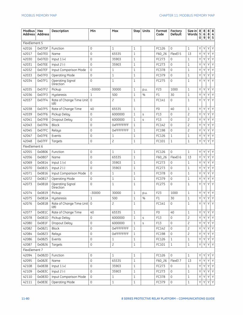
MODBUS MEMORY MAP CHAPTER 11: MODBUS MEMORY MAP
FlexElement 5
42016 0x07DF Function 0 1 1 FC126 0 1 Y Y Y Y
42017 0x07E0 Name 0 65535 1 F60_26 FlexEl 5 13 Y Y Y Y
42030 0x07ED Input 1 (+) 0 35903 1 FC273 0 1 Y Y Y Y
42031 0x07EE Input 2 (-) 0 35903 1 FC273 0 1 Y Y Y Y
42032 0x07EF Input Comparison Mode 0 1 1 FC378 0 1 Y Y Y Y
42033 0x07F0 Operating Mode 0 1 1 FC379 0 1 Y Y Y Y
42034 0x07F1 Operating Signal Direction
0 1 1 FC275 0 1 Y Y Y Y
42035 0x07F2 Pickup -30000 30000 1 p.u. F23 1000 1 Y Y Y Y
42036 0x07F3 Hysteresis 1 500 1 % F1 30 1 Y Y Y Y
42037 0x07F4 Rate of Change Time Unit (dt)
0 2 1 FC141 0 1 Y Y Y Y
42038 0x07F5 Rate of Change Time 40 65535 1 F0 40 1 Y Y Y Y
42039 0x07F6 Pickup Delay 0 6000000 1 s F13 0 2 Y Y Y Y
42041 0x07F8 Dropout Delay 0 6000000 1 s F13 0 2 Y Y Y Y
42043 0x07FA Block 0 0xFFFFFFFF 1 FC142 0 2 Y Y Y Y
42045 0x07FC Relays 0 0xFFFFFFFF 1 FC198 0 2 Y Y Y Y
42047 0x07FE Events 0 1 1 FC126 1 1 Y Y Y Y
42048 0x07FF Targets 0 2 1 FC101 1 1 Y Y Y Y
FlexElement 6
42055 0x0806 Function 0 1 1 FC126 0 1 Y Y Y Y
42056 0x0807 Name 0 65535 1 F60_26 FlexEl 6 13 Y Y Y Y
42069 0x0814 Input 1 (+) 0 35903 1 FC273 0 1 Y Y Y Y
42070 0x0815 Input 2 (-) 0 35903 1 FC273 0 1 Y Y Y Y
42071 0x0816 Input Comparison Mode 0 1 1 FC378 0 1 Y Y Y Y
42072 0x0817 Operating Mode 0 1 1 FC379 0 1 Y Y Y Y
42073 0x0818 Operating Signal Direction
0 1 1 FC275 0 1 Y Y Y Y
42074 0x0819 Pickup -30000 30000 1 p.u. F23 1000 1 Y Y Y Y
42075 0x081A Hysteresis 1 500 1 % F1 30 1 Y Y Y Y
42076 0x081B Rate of Change Time Unit (dt)
0 2 1 FC141 0 1 Y Y Y Y
42077 0x081C Rate of Change Time 40 65535 1 F0 40 1 Y Y Y Y
42078 0x081D Pickup Delay 0 6000000 1 s F13 0 2 Y Y Y Y
42080 0x081F Dropout Delay 0 6000000 1 s F13 0 2 Y Y Y Y
42082 0x0821 Block 0 0xFFFFFFFF 1 FC142 0 2 Y Y Y Y
42084 0x0823 Relays 0 0xFFFFFFFF 1 FC198 0 2 Y Y Y Y
42086 0x0825 Events 0 1 1 FC126 1 1 Y Y Y Y
42087 0x0826 Targets 0 2 1 FC101 1 1 Y Y Y Y
FlexElement 7
42094 0x082D Function 0 1 1 FC126 0 1 Y Y Y Y
42095 0x082E Name 0 65535 1 F60_26 FlexEl 7 13 Y Y Y Y
42108 0x083B Input 1 (+) 0 35903 1 FC273 0 1 Y Y Y Y
42109 0x083C Input 2 (-) 0 35903 1 FC273 0 1 Y Y Y Y
42110 0x083D Input Comparison Mode 0 1 1 FC378 0 1 Y Y Y Y
42111 0x083E Operating Mode 0 1 1 FC379 0 1 Y Y Y Y
Modbus Address
Hex Address
Description Min Max Step Units Format Code
Factory Default
Size in Words
850
869
889
845
11-80 8 SERIES PROTECTIVE RELAY PLATFORM – COMMUNICATIONS GUIDE
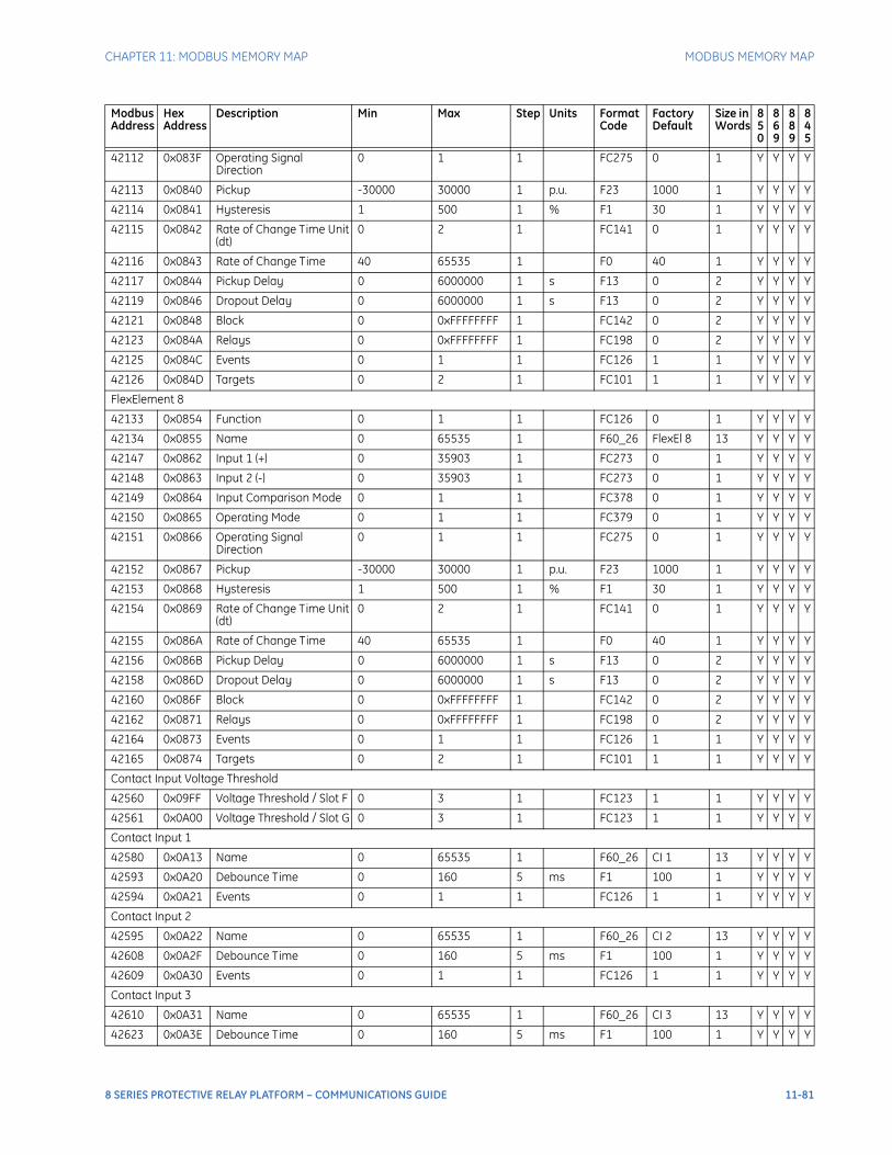
CHAPTER 11: MODBUS MEMORY MAP MODBUS MEMORY MAP
42112 0x083F Operating Signal Direction
0 1 1 FC275 0 1 Y Y Y Y
42113 0x0840 Pickup -30000 30000 1 p.u. F23 1000 1 Y Y Y Y
42114 0x0841 Hysteresis 1 500 1 % F1 30 1 Y Y Y Y
42115 0x0842 Rate of Change Time Unit (dt)
0 2 1 FC141 0 1 Y Y Y Y
42116 0x0843 Rate of Change Time 40 65535 1 F0 40 1 Y Y Y Y
42117 0x0844 Pickup Delay 0 6000000 1 s F13 0 2 Y Y Y Y
42119 0x0846 Dropout Delay 0 6000000 1 s F13 0 2 Y Y Y Y
42121 0x0848 Block 0 0xFFFFFFFF 1 FC142 0 2 Y Y Y Y
42123 0x084A Relays 0 0xFFFFFFFF 1 FC198 0 2 Y Y Y Y
42125 0x084C Events 0 1 1 FC126 1 1 Y Y Y Y
42126 0x084D Targets 0 2 1 FC101 1 1 Y Y Y Y
FlexElement 8
42133 0x0854 Function 0 1 1 FC126 0 1 Y Y Y Y
42134 0x0855 Name 0 65535 1 F60_26 FlexEl 8 13 Y Y Y Y
42147 0x0862 Input 1 (+) 0 35903 1 FC273 0 1 Y Y Y Y
42148 0x0863 Input 2 (-) 0 35903 1 FC273 0 1 Y Y Y Y
42149 0x0864 Input Comparison Mode 0 1 1 FC378 0 1 Y Y Y Y
42150 0x0865 Operating Mode 0 1 1 FC379 0 1 Y Y Y Y
42151 0x0866 Operating Signal Direction
0 1 1 FC275 0 1 Y Y Y Y
42152 0x0867 Pickup -30000 30000 1 p.u. F23 1000 1 Y Y Y Y
42153 0x0868 Hysteresis 1 500 1 % F1 30 1 Y Y Y Y
42154 0x0869 Rate of Change Time Unit (dt)
0 2 1 FC141 0 1 Y Y Y Y
42155 0x086A Rate of Change Time 40 65535 1 F0 40 1 Y Y Y Y
42156 0x086B Pickup Delay 0 6000000 1 s F13 0 2 Y Y Y Y
42158 0x086D Dropout Delay 0 6000000 1 s F13 0 2 Y Y Y Y
42160 0x086F Block 0 0xFFFFFFFF 1 FC142 0 2 Y Y Y Y
42162 0x0871 Relays 0 0xFFFFFFFF 1 FC198 0 2 Y Y Y Y
42164 0x0873 Events 0 1 1 FC126 1 1 Y Y Y Y
42165 0x0874 Targets 0 2 1 FC101 1 1 Y Y Y Y
Contact Input Voltage Threshold
42560 0x09FF Voltage Threshold / Slot F 0 3 1 FC123 1 1 Y Y Y Y
42561 0x0A00 Voltage Threshold / Slot G 0 3 1 FC123 1 1 Y Y Y Y
Contact Input 1
42580 0x0A13 Name 0 65535 1 F60_26 CI 1 13 Y Y Y Y
42593 0x0A20 Debounce Time 0 160 5 ms F1 100 1 Y Y Y Y
42594 0x0A21 Events 0 1 1 FC126 1 1 Y Y Y Y
Contact Input 2
42595 0x0A22 Name 0 65535 1 F60_26 CI 2 13 Y Y Y Y
42608 0x0A2F Debounce Time 0 160 5 ms F1 100 1 Y Y Y Y
42609 0x0A30 Events 0 1 1 FC126 1 1 Y Y Y Y
Contact Input 3
42610 0x0A31 Name 0 65535 1 F60_26 CI 3 13 Y Y Y Y
42623 0x0A3E Debounce Time 0 160 5 ms F1 100 1 Y Y Y Y
Modbus Address
Hex Address
Description Min Max Step Units Format Code
Factory Default
Size in Words
850
869
889
845
8 SERIES PROTECTIVE RELAY PLATFORM – COMMUNICATIONS GUIDE 11-81
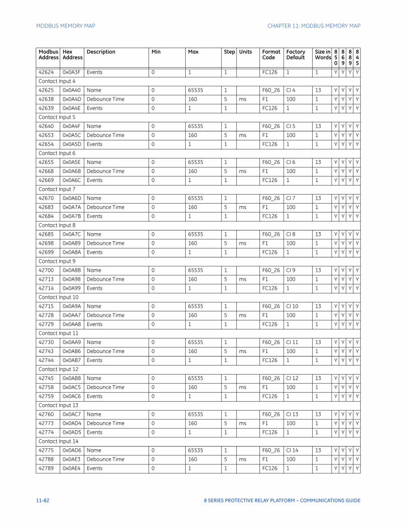
MODBUS MEMORY MAP CHAPTER 11: MODBUS MEMORY MAP
42624 0x0A3F Events 0 1 1 FC126 1 1 Y Y Y Y
Contact Input 4
42625 0x0A40 Name 0 65535 1 F60_26 CI 4 13 Y Y Y Y
42638 0x0A4D Debounce Time 0 160 5 ms F1 100 1 Y Y Y Y
42639 0x0A4E Events 0 1 1 FC126 1 1 Y Y Y Y
Contact Input 5
42640 0x0A4F Name 0 65535 1 F60_26 CI 5 13 Y Y Y Y
42653 0x0A5C Debounce Time 0 160 5 ms F1 100 1 Y Y Y Y
42654 0x0A5D Events 0 1 1 FC126 1 1 Y Y Y Y
Contact Input 6
42655 0x0A5E Name 0 65535 1 F60_26 CI 6 13 Y Y Y Y
42668 0x0A6B Debounce Time 0 160 5 ms F1 100 1 Y Y Y Y
42669 0x0A6C Events 0 1 1 FC126 1 1 Y Y Y Y
Contact Input 7
42670 0x0A6D Name 0 65535 1 F60_26 CI 7 13 Y Y Y Y
42683 0x0A7A Debounce Time 0 160 5 ms F1 100 1 Y Y Y Y
42684 0x0A7B Events 0 1 1 FC126 1 1 Y Y Y Y
Contact Input 8
42685 0x0A7C Name 0 65535 1 F60_26 CI 8 13 Y Y Y Y
42698 0x0A89 Debounce Time 0 160 5 ms F1 100 1 Y Y Y Y
42699 0x0A8A Events 0 1 1 FC126 1 1 Y Y Y Y
Contact Input 9
42700 0x0A8B Name 0 65535 1 F60_26 CI 9 13 Y Y Y Y
42713 0x0A98 Debounce Time 0 160 5 ms F1 100 1 Y Y Y Y
42714 0x0A99 Events 0 1 1 FC126 1 1 Y Y Y Y
Contact Input 10
42715 0x0A9A Name 0 65535 1 F60_26 CI 10 13 Y Y Y Y
42728 0x0AA7 Debounce Time 0 160 5 ms F1 100 1 Y Y Y Y
42729 0x0AA8 Events 0 1 1 FC126 1 1 Y Y Y Y
Contact Input 11
42730 0x0AA9 Name 0 65535 1 F60_26 CI 11 13 Y Y Y Y
42743 0x0AB6 Debounce Time 0 160 5 ms F1 100 1 Y Y Y Y
42744 0x0AB7 Events 0 1 1 FC126 1 1 Y Y Y Y
Contact Input 12
42745 0x0AB8 Name 0 65535 1 F60_26 CI 12 13 Y Y Y Y
42758 0x0AC5 Debounce Time 0 160 5 ms F1 100 1 Y Y Y Y
42759 0x0AC6 Events 0 1 1 FC126 1 1 Y Y Y Y
Contact Input 13
42760 0x0AC7 Name 0 65535 1 F60_26 CI 13 13 Y Y Y Y
42773 0x0AD4 Debounce Time 0 160 5 ms F1 100 1 Y Y Y Y
42774 0x0AD5 Events 0 1 1 FC126 1 1 Y Y Y Y
Contact Input 14
42775 0x0AD6 Name 0 65535 1 F60_26 CI 14 13 Y Y Y Y
42788 0x0AE3 Debounce Time 0 160 5 ms F1 100 1 Y Y Y Y
42789 0x0AE4 Events 0 1 1 FC126 1 1 Y Y Y Y
Modbus Address
Hex Address
Description Min Max Step Units Format Code
Factory Default
Size in Words
850
869
889
845
11-82 8 SERIES PROTECTIVE RELAY PLATFORM – COMMUNICATIONS GUIDE

CHAPTER 11: MODBUS MEMORY MAP MODBUS MEMORY MAP
Contact Input 15
42790 0x0AE5 Name 0 65535 1 F60_26 CI 15 13 Y Y Y Y
42803 0x0AF2 Debounce Time 0 160 5 ms F1 100 1 Y Y Y Y
42804 0x0AF3 Events 0 1 1 FC126 1 1 Y Y Y Y
Contact Input 16
42805 0x0AF4 Name 0 65535 1 F60_26 CI 16 13 Y Y Y Y
42818 0x0B01 Debounce Time 0 160 5 ms F1 100 1 Y Y Y Y
42819 0x0B02 Events 0 1 1 FC126 1 1 Y Y Y Y
Contact Input 17
42820 0x0B03 Name 0 65535 1 F60_26 CI 17 13 Y Y Y Y
42833 0x0B10 Debounce Time 0 160 5 ms F1 100 1 Y Y Y Y
42834 0x0B11 Events 0 1 1 FC126 1 1 Y Y Y Y
Contact Input 18
42835 0x0B12 Name 0 65535 1 F60_26 CI 18 13 Y Y Y Y
42848 0x0B1F Debounce Time 0 160 5 ms F1 100 1 Y Y Y Y
42849 0x0B20 Events 0 1 1 FC126 1 1 Y Y Y Y
Contact Input 19
42850 0x0B21 Name 0 65535 1 F60_26 CI 19 13 Y Y Y Y
42863 0x0B2E Debounce Time 0 160 5 ms F1 100 1 Y Y Y Y
42864 0x0B2F Events 0 1 1 FC126 1 1 Y Y Y Y
Contact Input 20
42865 0x0B30 Name 0 65535 1 F60_26 CI 20 13 Y Y Y Y
42878 0x0B3D Debounce Time 0 160 5 ms F1 100 1 Y Y Y Y
42879 0x0B3E Events 0 1 1 FC126 1 1 Y Y Y Y
Contact Input 21
42880 0x0B3F Name 0 65535 1 F60_26 CI 21 13 Y Y Y Y
42893 0x0B4C Debounce Time 0 160 5 ms F1 100 1 Y Y Y Y
42894 0x0B4D Events 0 1 1 FC126 1 1 Y Y Y Y
Contact Input 22
42895 0x0B4E Name 0 65535 1 F60_26 CI 22 13 Y Y Y Y
42908 0x0B5B Debounce Time 0 160 5 ms F1 100 1 Y Y Y Y
42909 0x0B5C Events 0 1 1 FC126 1 1 Y Y Y Y
Contact Input 23
42910 0x0B5D Name 0 65535 1 F60_26 CI 23 13 Y Y Y Y
42923 0x0B6A Debounce Time 0 160 5 ms F1 100 1 Y Y Y Y
42924 0x0B6B Events 0 1 1 FC126 1 1 Y Y Y Y
Contact Input 24
42925 0x0B6C Name 0 65535 1 F60_26 CI 24 13 Y Y Y Y
42938 0x0B79 Debounce Time 0 160 5 ms F1 100 1 Y Y Y Y
42939 0x0B7A Events 0 1 1 FC126 1 1 Y Y Y Y
Contact Input 25
42940 0x0B7B Name 0 65535 1 F60_26 CI 25 13 Y Y Y Y
42953 0x0B88 Debounce Time 0 160 5 ms F1 100 1 Y Y Y Y
42954 0x0B89 Events 0 1 1 FC126 1 1 Y Y Y Y
Contact Input 26
Modbus Address
Hex Address
Description Min Max Step Units Format Code
Factory Default
Size in Words
850
869
889
845
8 SERIES PROTECTIVE RELAY PLATFORM – COMMUNICATIONS GUIDE 11-83
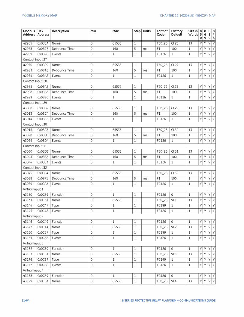
MODBUS MEMORY MAP CHAPTER 11: MODBUS MEMORY MAP
42955 0x0B8A Name 0 65535 1 F60_26 CI 26 13 Y Y Y Y
42968 0x0B97 Debounce Time 0 160 5 ms F1 100 1 Y Y Y Y
42969 0x0B98 Events 0 1 1 FC126 1 1 Y Y Y Y
Contact Input 27
42970 0x0B99 Name 0 65535 1 F60_26 CI 27 13 Y Y Y Y
42983 0x0BA6 Debounce Time 0 160 5 ms F1 100 1 Y Y Y Y
42984 0x0BA7 Events 0 1 1 FC126 1 1 Y Y Y Y
Contact Input 28
42985 0x0BA8 Name 0 65535 1 F60_26 CI 28 13 Y Y Y Y
42998 0x0BB5 Debounce Time 0 160 5 ms F1 100 1 Y Y Y Y
42999 0x0BB6 Events 0 1 1 FC126 1 1 Y Y Y Y
Contact Input 29
43000 0x0BB7 Name 0 65535 1 F60_26 CI 29 13 Y Y Y Y
43013 0x0BC4 Debounce Time 0 160 5 ms F1 100 1 Y Y Y Y
43014 0x0BC5 Events 0 1 1 FC126 1 1 Y Y Y Y
Contact Input 30
43015 0x0BC6 Name 0 65535 1 F60_26 CI 30 13 Y Y Y Y
43028 0x0BD3 Debounce Time 0 160 5 ms F1 100 1 Y Y Y Y
43029 0x0BD4 Events 0 1 1 FC126 1 1 Y Y Y Y
Contact Input 31
43030 0x0BD5 Name 0 65535 1 F60_26 CI 31 13 Y Y Y Y
43043 0x0BE2 Debounce Time 0 160 5 ms F1 100 1 Y Y Y Y
43044 0x0BE3 Events 0 1 1 FC126 1 1 Y Y Y Y
Contact Input 32
43045 0x0BE4 Name 0 65535 1 F60_26 CI 32 13 Y Y Y Y
43058 0x0BF1 Debounce Time 0 160 5 ms F1 100 1 Y Y Y Y
43059 0x0BF2 Events 0 1 1 FC126 1 1 Y Y Y Y
Virtual Input 1
43130 0x0C39 Function 0 1 1 FC126 0 1 Y Y Y Y
43131 0x0C3A Name 0 65535 1 F60_26 VI 1 13 Y Y Y Y
43144 0x0C47 Type 0 1 1 FC199 1 1 Y Y Y Y
43145 0x0C48 Events 0 1 1 FC126 1 1 Y Y Y Y
Virtual Input 2
43146 0x0C49 Function 0 1 1 FC126 0 1 Y Y Y Y
43147 0x0C4A Name 0 65535 1 F60_26 VI 2 13 Y Y Y Y
43160 0x0C57 Type 0 1 1 FC199 1 1 Y Y Y Y
43161 0x0C58 Events 0 1 1 FC126 1 1 Y Y Y Y
Virtual Input 3
43162 0x0C59 Function 0 1 1 FC126 0 1 Y Y Y Y
43163 0x0C5A Name 0 65535 1 F60_26 VI 3 13 Y Y Y Y
43176 0x0C67 Type 0 1 1 FC199 1 1 Y Y Y Y
43177 0x0C68 Events 0 1 1 FC126 1 1 Y Y Y Y
Virtual Input 4
43178 0x0C69 Function 0 1 1 FC126 0 1 Y Y Y Y
43179 0x0C6A Name 0 65535 1 F60_26 VI 4 13 Y Y Y Y
Modbus Address
Hex Address
Description Min Max Step Units Format Code
Factory Default
Size in Words
850
869
889
845
11-84 8 SERIES PROTECTIVE RELAY PLATFORM – COMMUNICATIONS GUIDE
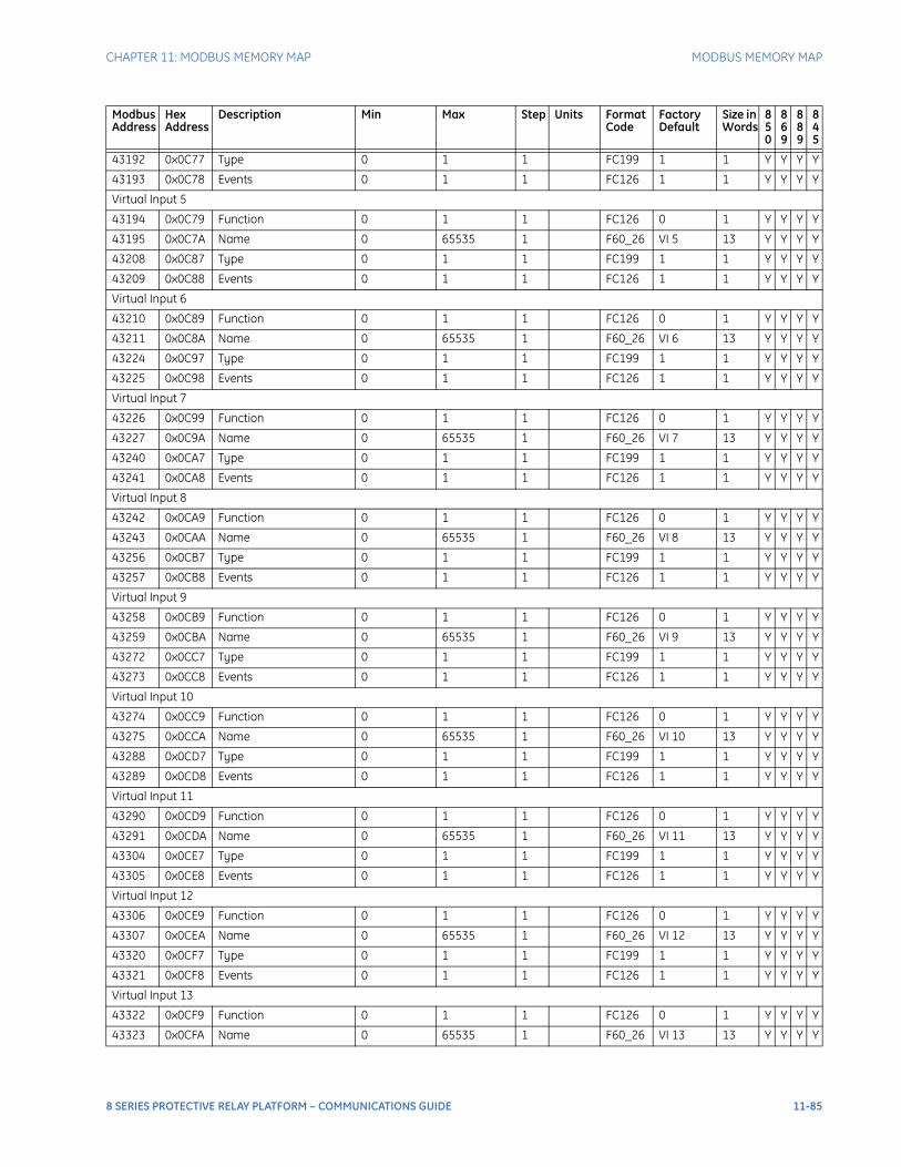
CHAPTER 11: MODBUS MEMORY MAP MODBUS MEMORY MAP
43192 0x0C77 Type 0 1 1 FC199 1 1 Y Y Y Y
43193 0x0C78 Events 0 1 1 FC126 1 1 Y Y Y Y
Virtual Input 5
43194 0x0C79 Function 0 1 1 FC126 0 1 Y Y Y Y
43195 0x0C7A Name 0 65535 1 F60_26 VI 5 13 Y Y Y Y
43208 0x0C87 Type 0 1 1 FC199 1 1 Y Y Y Y
43209 0x0C88 Events 0 1 1 FC126 1 1 Y Y Y Y
Virtual Input 6
43210 0x0C89 Function 0 1 1 FC126 0 1 Y Y Y Y
43211 0x0C8A Name 0 65535 1 F60_26 VI 6 13 Y Y Y Y
43224 0x0C97 Type 0 1 1 FC199 1 1 Y Y Y Y
43225 0x0C98 Events 0 1 1 FC126 1 1 Y Y Y Y
Virtual Input 7
43226 0x0C99 Function 0 1 1 FC126 0 1 Y Y Y Y
43227 0x0C9A Name 0 65535 1 F60_26 VI 7 13 Y Y Y Y
43240 0x0CA7 Type 0 1 1 FC199 1 1 Y Y Y Y
43241 0x0CA8 Events 0 1 1 FC126 1 1 Y Y Y Y
Virtual Input 8
43242 0x0CA9 Function 0 1 1 FC126 0 1 Y Y Y Y
43243 0x0CAA Name 0 65535 1 F60_26 VI 8 13 Y Y Y Y
43256 0x0CB7 Type 0 1 1 FC199 1 1 Y Y Y Y
43257 0x0CB8 Events 0 1 1 FC126 1 1 Y Y Y Y
Virtual Input 9
43258 0x0CB9 Function 0 1 1 FC126 0 1 Y Y Y Y
43259 0x0CBA Name 0 65535 1 F60_26 VI 9 13 Y Y Y Y
43272 0x0CC7 Type 0 1 1 FC199 1 1 Y Y Y Y
43273 0x0CC8 Events 0 1 1 FC126 1 1 Y Y Y Y
Virtual Input 10
43274 0x0CC9 Function 0 1 1 FC126 0 1 Y Y Y Y
43275 0x0CCA Name 0 65535 1 F60_26 VI 10 13 Y Y Y Y
43288 0x0CD7 Type 0 1 1 FC199 1 1 Y Y Y Y
43289 0x0CD8 Events 0 1 1 FC126 1 1 Y Y Y Y
Virtual Input 11
43290 0x0CD9 Function 0 1 1 FC126 0 1 Y Y Y Y
43291 0x0CDA Name 0 65535 1 F60_26 VI 11 13 Y Y Y Y
43304 0x0CE7 Type 0 1 1 FC199 1 1 Y Y Y Y
43305 0x0CE8 Events 0 1 1 FC126 1 1 Y Y Y Y
Virtual Input 12
43306 0x0CE9 Function 0 1 1 FC126 0 1 Y Y Y Y
43307 0x0CEA Name 0 65535 1 F60_26 VI 12 13 Y Y Y Y
43320 0x0CF7 Type 0 1 1 FC199 1 1 Y Y Y Y
43321 0x0CF8 Events 0 1 1 FC126 1 1 Y Y Y Y
Virtual Input 13
43322 0x0CF9 Function 0 1 1 FC126 0 1 Y Y Y Y
43323 0x0CFA Name 0 65535 1 F60_26 VI 13 13 Y Y Y Y
Modbus Address
Hex Address
Description Min Max Step Units Format Code
Factory Default
Size in Words
850
869
889
845
8 SERIES PROTECTIVE RELAY PLATFORM – COMMUNICATIONS GUIDE 11-85
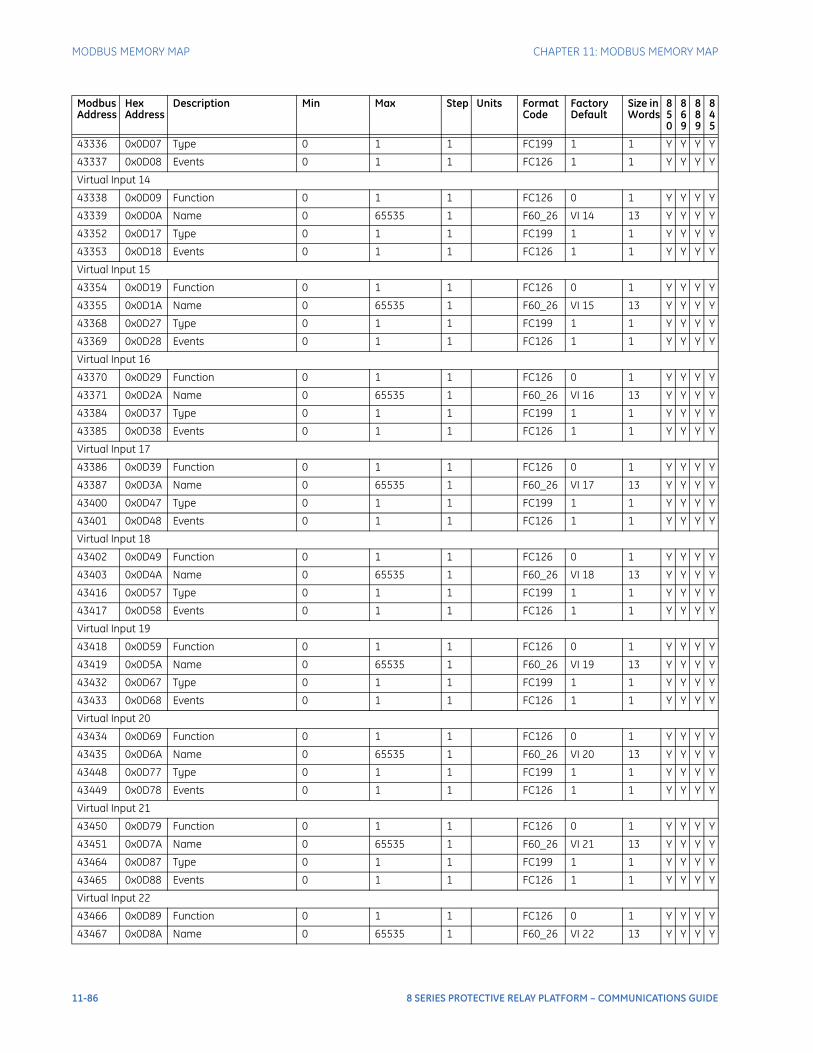
MODBUS MEMORY MAP CHAPTER 11: MODBUS MEMORY MAP
43336 0x0D07 Type 0 1 1 FC199 1 1 Y Y Y Y
43337 0x0D08 Events 0 1 1 FC126 1 1 Y Y Y Y
Virtual Input 14
43338 0x0D09 Function 0 1 1 FC126 0 1 Y Y Y Y
43339 0x0D0A Name 0 65535 1 F60_26 VI 14 13 Y Y Y Y
43352 0x0D17 Type 0 1 1 FC199 1 1 Y Y Y Y
43353 0x0D18 Events 0 1 1 FC126 1 1 Y Y Y Y
Virtual Input 15
43354 0x0D19 Function 0 1 1 FC126 0 1 Y Y Y Y
43355 0x0D1A Name 0 65535 1 F60_26 VI 15 13 Y Y Y Y
43368 0x0D27 Type 0 1 1 FC199 1 1 Y Y Y Y
43369 0x0D28 Events 0 1 1 FC126 1 1 Y Y Y Y
Virtual Input 16
43370 0x0D29 Function 0 1 1 FC126 0 1 Y Y Y Y
43371 0x0D2A Name 0 65535 1 F60_26 VI 16 13 Y Y Y Y
43384 0x0D37 Type 0 1 1 FC199 1 1 Y Y Y Y
43385 0x0D38 Events 0 1 1 FC126 1 1 Y Y Y Y
Virtual Input 17
43386 0x0D39 Function 0 1 1 FC126 0 1 Y Y Y Y
43387 0x0D3A Name 0 65535 1 F60_26 VI 17 13 Y Y Y Y
43400 0x0D47 Type 0 1 1 FC199 1 1 Y Y Y Y
43401 0x0D48 Events 0 1 1 FC126 1 1 Y Y Y Y
Virtual Input 18
43402 0x0D49 Function 0 1 1 FC126 0 1 Y Y Y Y
43403 0x0D4A Name 0 65535 1 F60_26 VI 18 13 Y Y Y Y
43416 0x0D57 Type 0 1 1 FC199 1 1 Y Y Y Y
43417 0x0D58 Events 0 1 1 FC126 1 1 Y Y Y Y
Virtual Input 19
43418 0x0D59 Function 0 1 1 FC126 0 1 Y Y Y Y
43419 0x0D5A Name 0 65535 1 F60_26 VI 19 13 Y Y Y Y
43432 0x0D67 Type 0 1 1 FC199 1 1 Y Y Y Y
43433 0x0D68 Events 0 1 1 FC126 1 1 Y Y Y Y
Virtual Input 20
43434 0x0D69 Function 0 1 1 FC126 0 1 Y Y Y Y
43435 0x0D6A Name 0 65535 1 F60_26 VI 20 13 Y Y Y Y
43448 0x0D77 Type 0 1 1 FC199 1 1 Y Y Y Y
43449 0x0D78 Events 0 1 1 FC126 1 1 Y Y Y Y
Virtual Input 21
43450 0x0D79 Function 0 1 1 FC126 0 1 Y Y Y Y
43451 0x0D7A Name 0 65535 1 F60_26 VI 21 13 Y Y Y Y
43464 0x0D87 Type 0 1 1 FC199 1 1 Y Y Y Y
43465 0x0D88 Events 0 1 1 FC126 1 1 Y Y Y Y
Virtual Input 22
43466 0x0D89 Function 0 1 1 FC126 0 1 Y Y Y Y
43467 0x0D8A Name 0 65535 1 F60_26 VI 22 13 Y Y Y Y
Modbus Address
Hex Address
Description Min Max Step Units Format Code
Factory Default
Size in Words
850
869
889
845
11-86 8 SERIES PROTECTIVE RELAY PLATFORM – COMMUNICATIONS GUIDE
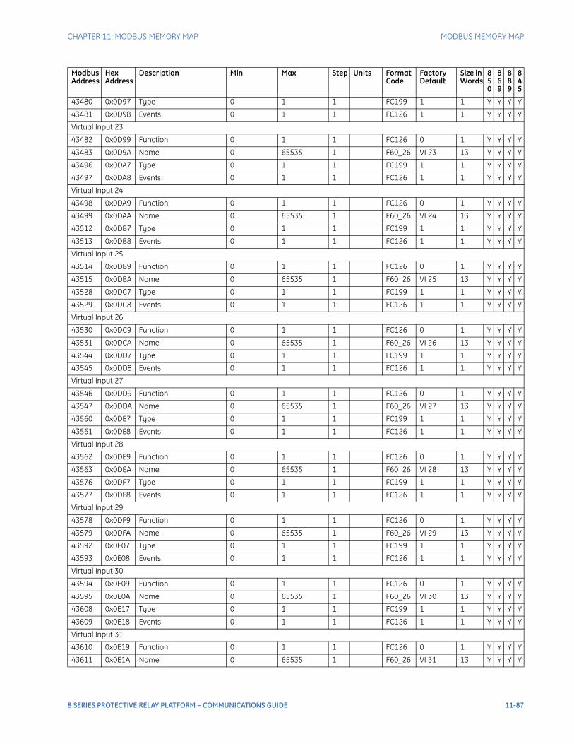
CHAPTER 11: MODBUS MEMORY MAP MODBUS MEMORY MAP
43480 0x0D97 Type 0 1 1 FC199 1 1 Y Y Y Y
43481 0x0D98 Events 0 1 1 FC126 1 1 Y Y Y Y
Virtual Input 23
43482 0x0D99 Function 0 1 1 FC126 0 1 Y Y Y Y
43483 0x0D9A Name 0 65535 1 F60_26 VI 23 13 Y Y Y Y
43496 0x0DA7 Type 0 1 1 FC199 1 1 Y Y Y Y
43497 0x0DA8 Events 0 1 1 FC126 1 1 Y Y Y Y
Virtual Input 24
43498 0x0DA9 Function 0 1 1 FC126 0 1 Y Y Y Y
43499 0x0DAA Name 0 65535 1 F60_26 VI 24 13 Y Y Y Y
43512 0x0DB7 Type 0 1 1 FC199 1 1 Y Y Y Y
43513 0x0DB8 Events 0 1 1 FC126 1 1 Y Y Y Y
Virtual Input 25
43514 0x0DB9 Function 0 1 1 FC126 0 1 Y Y Y Y
43515 0x0DBA Name 0 65535 1 F60_26 VI 25 13 Y Y Y Y
43528 0x0DC7 Type 0 1 1 FC199 1 1 Y Y Y Y
43529 0x0DC8 Events 0 1 1 FC126 1 1 Y Y Y Y
Virtual Input 26
43530 0x0DC9 Function 0 1 1 FC126 0 1 Y Y Y Y
43531 0x0DCA Name 0 65535 1 F60_26 VI 26 13 Y Y Y Y
43544 0x0DD7 Type 0 1 1 FC199 1 1 Y Y Y Y
43545 0x0DD8 Events 0 1 1 FC126 1 1 Y Y Y Y
Virtual Input 27
43546 0x0DD9 Function 0 1 1 FC126 0 1 Y Y Y Y
43547 0x0DDA Name 0 65535 1 F60_26 VI 27 13 Y Y Y Y
43560 0x0DE7 Type 0 1 1 FC199 1 1 Y Y Y Y
43561 0x0DE8 Events 0 1 1 FC126 1 1 Y Y Y Y
Virtual Input 28
43562 0x0DE9 Function 0 1 1 FC126 0 1 Y Y Y Y
43563 0x0DEA Name 0 65535 1 F60_26 VI 28 13 Y Y Y Y
43576 0x0DF7 Type 0 1 1 FC199 1 1 Y Y Y Y
43577 0x0DF8 Events 0 1 1 FC126 1 1 Y Y Y Y
Virtual Input 29
43578 0x0DF9 Function 0 1 1 FC126 0 1 Y Y Y Y
43579 0x0DFA Name 0 65535 1 F60_26 VI 29 13 Y Y Y Y
43592 0x0E07 Type 0 1 1 FC199 1 1 Y Y Y Y
43593 0x0E08 Events 0 1 1 FC126 1 1 Y Y Y Y
Virtual Input 30
43594 0x0E09 Function 0 1 1 FC126 0 1 Y Y Y Y
43595 0x0E0A Name 0 65535 1 F60_26 VI 30 13 Y Y Y Y
43608 0x0E17 Type 0 1 1 FC199 1 1 Y Y Y Y
43609 0x0E18 Events 0 1 1 FC126 1 1 Y Y Y Y
Virtual Input 31
43610 0x0E19 Function 0 1 1 FC126 0 1 Y Y Y Y
43611 0x0E1A Name 0 65535 1 F60_26 VI 31 13 Y Y Y Y
Modbus Address
Hex Address
Description Min Max Step Units Format Code
Factory Default
Size in Words
850
869
889
845
8 SERIES PROTECTIVE RELAY PLATFORM – COMMUNICATIONS GUIDE 11-87
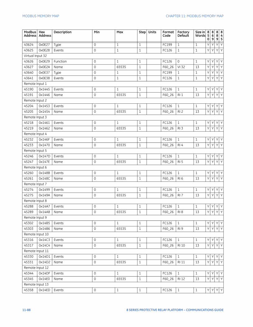
MODBUS MEMORY MAP CHAPTER 11: MODBUS MEMORY MAP
43624 0x0E27 Type 0 1 1 FC199 1 1 Y Y Y Y
43625 0x0E28 Events 0 1 1 FC126 1 1 Y Y Y Y
Virtual Input 32
43626 0x0E29 Function 0 1 1 FC126 0 1 Y Y Y Y
43627 0x0E2A Name 0 65535 1 F60_26 VI 32 13 Y Y Y Y
43640 0x0E37 Type 0 1 1 FC199 1 1 Y Y Y Y
43641 0x0E38 Events 0 1 1 FC126 1 1 Y Y Y Y
Remote Input 1
45190 0x1445 Events 0 1 1 FC126 1 1 Y Y Y Y
45191 0x1446 Name 0 65535 1 F60_26 RI 1 13 Y Y Y Y
Remote Input 2
45204 0x1453 Events 0 1 1 FC126 1 1 Y Y Y Y
45205 0x1454 Name 0 65535 1 F60_26 RI 2 13 Y Y Y Y
Remote Input 3
45218 0x1461 Events 0 1 1 FC126 1 1 Y Y Y Y
45219 0x1462 Name 0 65535 1 F60_26 RI 3 13 Y Y Y Y
Remote Input 4
45232 0x146F Events 0 1 1 FC126 1 1 Y Y Y Y
45233 0x1470 Name 0 65535 1 F60_26 RI 4 13 Y Y Y Y
Remote Input 5
45246 0x147D Events 0 1 1 FC126 1 1 Y Y Y Y
45247 0x147E Name 0 65535 1 F60_26 RI 5 13 Y Y Y Y
Remote Input 6
45260 0x148B Events 0 1 1 FC126 1 1 Y Y Y Y
45261 0x148C Name 0 65535 1 F60_26 RI 6 13 Y Y Y Y
Remote Input 7
45274 0x1499 Events 0 1 1 FC126 1 1 Y Y Y Y
45275 0x149A Name 0 65535 1 F60_26 RI 7 13 Y Y Y Y
Remote Input 8
45288 0x14A7 Events 0 1 1 FC126 1 1 Y Y Y Y
45289 0x14A8 Name 0 65535 1 F60_26 RI 8 13 Y Y Y Y
Remote Input 9
45302 0x14B5 Events 0 1 1 FC126 1 1 Y Y Y Y
45303 0x14B6 Name 0 65535 1 F60_26 RI 9 13 Y Y Y Y
Remote Input 10
45316 0x14C3 Events 0 1 1 FC126 1 1 Y Y Y Y
45317 0x14C4 Name 0 65535 1 F60_26 RI 10 13 Y Y Y Y
Remote Input 11
45330 0x14D1 Events 0 1 1 FC126 1 1 Y Y Y Y
45331 0x14D2 Name 0 65535 1 F60_26 RI 11 13 Y Y Y Y
Remote Input 12
45344 0x14DF Events 0 1 1 FC126 1 1 Y Y Y Y
45345 0x14E0 Name 0 65535 1 F60_26 RI 12 13 Y Y Y Y
Remote Input 13
45358 0x14ED Events 0 1 1 FC126 1 1 Y Y Y Y
Modbus Address
Hex Address
Description Min Max Step Units Format Code
Factory Default
Size in Words
850
869
889
845
11-88 8 SERIES PROTECTIVE RELAY PLATFORM – COMMUNICATIONS GUIDE
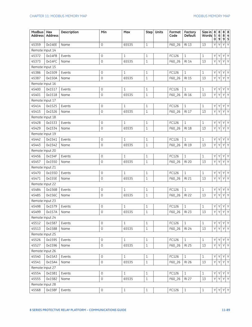
CHAPTER 11: MODBUS MEMORY MAP MODBUS MEMORY MAP
45359 0x14EE Name 0 65535 1 F60_26 RI 13 13 Y Y Y Y
Remote Input 14
45372 0x14FB Events 0 1 1 FC126 1 1 Y Y Y Y
45373 0x14FC Name 0 65535 1 F60_26 RI 14 13 Y Y Y Y
Remote Input 15
45386 0x1509 Events 0 1 1 FC126 1 1 Y Y Y Y
45387 0x150A Name 0 65535 1 F60_26 RI 15 13 Y Y Y Y
Remote Input 16
45400 0x1517 Events 0 1 1 FC126 1 1 Y Y Y Y
45401 0x1518 Name 0 65535 1 F60_26 RI 16 13 Y Y Y Y
Remote Input 17
45414 0x1525 Events 0 1 1 FC126 1 1 Y Y Y Y
45415 0x1526 Name 0 65535 1 F60_26 RI 17 13 Y Y Y Y
Remote Input 18
45428 0x1533 Events 0 1 1 FC126 1 1 Y Y Y Y
45429 0x1534 Name 0 65535 1 F60_26 RI 18 13 Y Y Y Y
Remote Input 19
45442 0x1541 Events 0 1 1 FC126 1 1 Y Y Y Y
45443 0x1542 Name 0 65535 1 F60_26 RI 19 13 Y Y Y Y
Remote Input 20
45456 0x154F Events 0 1 1 FC126 1 1 Y Y Y Y
45457 0x1550 Name 0 65535 1 F60_26 RI 20 13 Y Y Y Y
Remote Input 21
45470 0x155D Events 0 1 1 FC126 1 1 Y Y Y Y
45471 0x155E Name 0 65535 1 F60_26 RI 21 13 Y Y Y Y
Remote Input 22
45484 0x156B Events 0 1 1 FC126 1 1 Y Y Y Y
45485 0x156C Name 0 65535 1 F60_26 RI 22 13 Y Y Y Y
Remote Input 23
45498 0x1579 Events 0 1 1 FC126 1 1 Y Y Y Y
45499 0x157A Name 0 65535 1 F60_26 RI 23 13 Y Y Y Y
Remote Input 24
45512 0x1587 Events 0 1 1 FC126 1 1 Y Y Y Y
45513 0x1588 Name 0 65535 1 F60_26 RI 24 13 Y Y Y Y
Remote Input 25
45526 0x1595 Events 0 1 1 FC126 1 1 Y Y Y Y
45527 0x1596 Name 0 65535 1 F60_26 RI 25 13 Y Y Y Y
Remote Input 26
45540 0x15A3 Events 0 1 1 FC126 1 1 Y Y Y Y
45541 0x15A4 Name 0 65535 1 F60_26 RI 26 13 Y Y Y Y
Remote Input 27
45554 0x15B1 Events 0 1 1 FC126 1 1 Y Y Y Y
45555 0x15B2 Name 0 65535 1 F60_26 RI 27 13 Y Y Y Y
Remote Input 28
45568 0x15BF Events 0 1 1 FC126 1 1 Y Y Y Y
Modbus Address
Hex Address
Description Min Max Step Units Format Code
Factory Default
Size in Words
850
869
889
845
8 SERIES PROTECTIVE RELAY PLATFORM – COMMUNICATIONS GUIDE 11-89
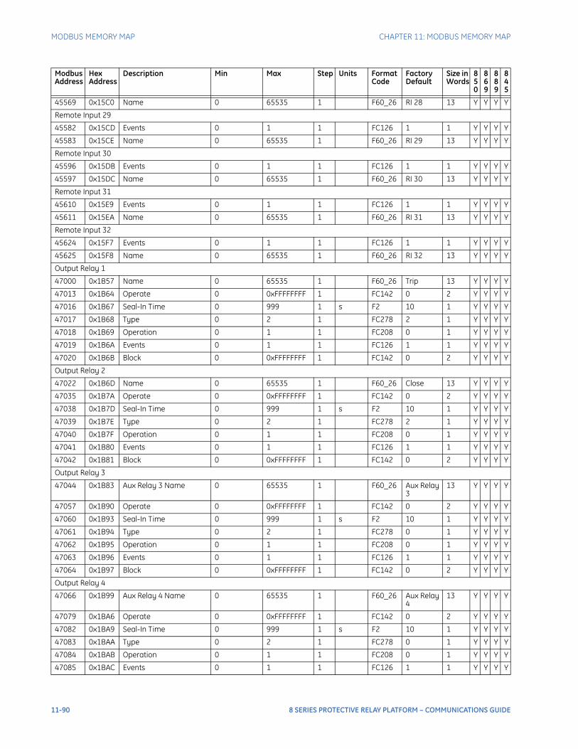
MODBUS MEMORY MAP CHAPTER 11: MODBUS MEMORY MAP
45569 0x15C0 Name 0 65535 1 F60_26 RI 28 13 Y Y Y Y
Remote Input 29
45582 0x15CD Events 0 1 1 FC126 1 1 Y Y Y Y
45583 0x15CE Name 0 65535 1 F60_26 RI 29 13 Y Y Y Y
Remote Input 30
45596 0x15DB Events 0 1 1 FC126 1 1 Y Y Y Y
45597 0x15DC Name 0 65535 1 F60_26 RI 30 13 Y Y Y Y
Remote Input 31
45610 0x15E9 Events 0 1 1 FC126 1 1 Y Y Y Y
45611 0x15EA Name 0 65535 1 F60_26 RI 31 13 Y Y Y Y
Remote Input 32
45624 0x15F7 Events 0 1 1 FC126 1 1 Y Y Y Y
45625 0x15F8 Name 0 65535 1 F60_26 RI 32 13 Y Y Y Y
Output Relay 1
47000 0x1B57 Name 0 65535 1 F60_26 Trip 13 Y Y Y Y
47013 0x1B64 Operate 0 0xFFFFFFFF 1 FC142 0 2 Y Y Y Y
47016 0x1B67 Seal-In Time 0 999 1 s F2 10 1 Y Y Y Y
47017 0x1B68 Type 0 2 1 FC278 2 1 Y Y Y Y
47018 0x1B69 Operation 0 1 1 FC208 0 1 Y Y Y Y
47019 0x1B6A Events 0 1 1 FC126 1 1 Y Y Y Y
47020 0x1B6B Block 0 0xFFFFFFFF 1 FC142 0 2 Y Y Y Y
Output Relay 2
47022 0x1B6D Name 0 65535 1 F60_26 Close 13 Y Y Y Y
47035 0x1B7A Operate 0 0xFFFFFFFF 1 FC142 0 2 Y Y Y Y
47038 0x1B7D Seal-In Time 0 999 1 s F2 10 1 Y Y Y Y
47039 0x1B7E Type 0 2 1 FC278 2 1 Y Y Y Y
47040 0x1B7F Operation 0 1 1 FC208 0 1 Y Y Y Y
47041 0x1B80 Events 0 1 1 FC126 1 1 Y Y Y Y
47042 0x1B81 Block 0 0xFFFFFFFF 1 FC142 0 2 Y Y Y Y
Output Relay 3
47044 0x1B83 Aux Relay 3 Name 0 65535 1 F60_26 Aux Relay 3
13 Y Y Y Y
47057 0x1B90 Operate 0 0xFFFFFFFF 1 FC142 0 2 Y Y Y Y
47060 0x1B93 Seal-In Time 0 999 1 s F2 10 1 Y Y Y Y
47061 0x1B94 Type 0 2 1 FC278 0 1 Y Y Y Y
47062 0x1B95 Operation 0 1 1 FC208 0 1 Y Y Y Y
47063 0x1B96 Events 0 1 1 FC126 1 1 Y Y Y Y
47064 0x1B97 Block 0 0xFFFFFFFF 1 FC142 0 2 Y Y Y Y
Output Relay 4
47066 0x1B99 Aux Relay 4 Name 0 65535 1 F60_26 Aux Relay 4
13 Y Y Y Y
47079 0x1BA6 Operate 0 0xFFFFFFFF 1 FC142 0 2 Y Y Y Y
47082 0x1BA9 Seal-In Time 0 999 1 s F2 10 1 Y Y Y Y
47083 0x1BAA Type 0 2 1 FC278 0 1 Y Y Y Y
47084 0x1BAB Operation 0 1 1 FC208 0 1 Y Y Y Y
47085 0x1BAC Events 0 1 1 FC126 1 1 Y Y Y Y
Modbus Address
Hex Address
Description Min Max Step Units Format Code
Factory Default
Size in Words
850
869
889
845
11-90 8 SERIES PROTECTIVE RELAY PLATFORM – COMMUNICATIONS GUIDE
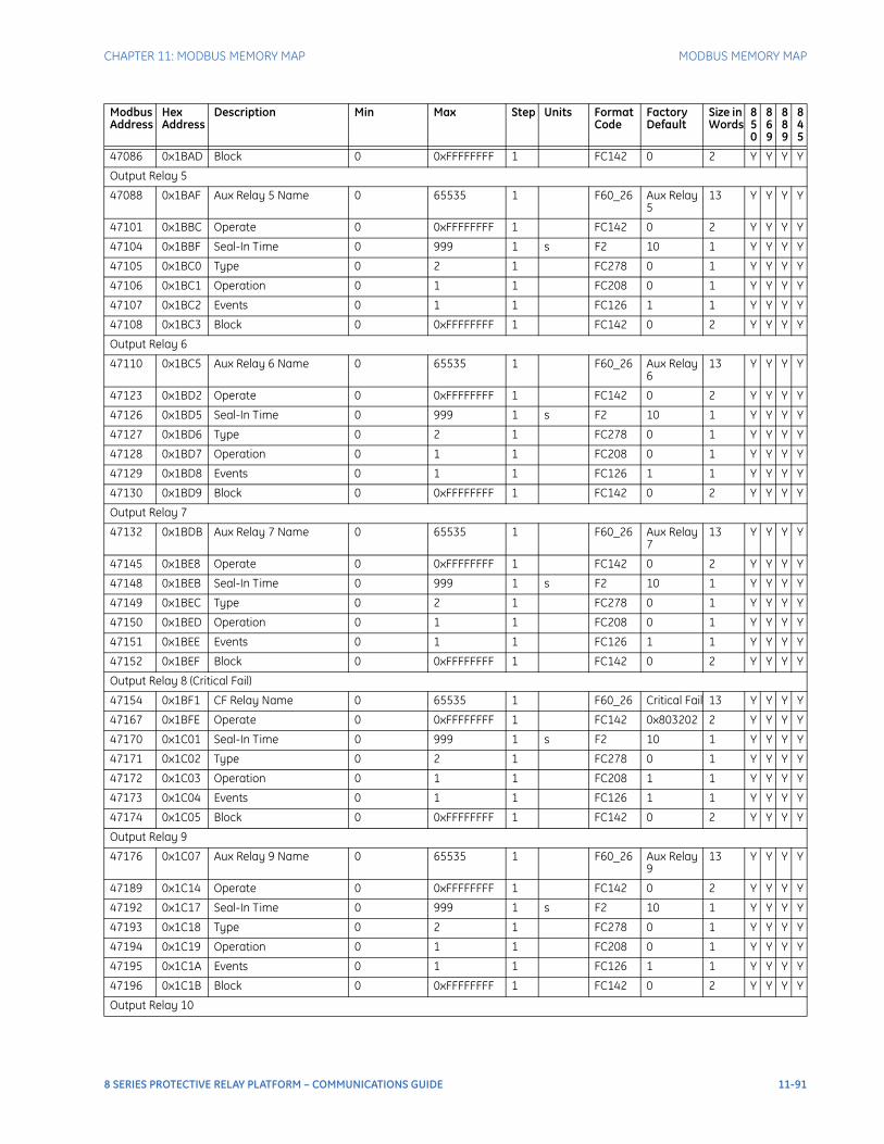
CHAPTER 11: MODBUS MEMORY MAP MODBUS MEMORY MAP
47086 0x1BAD Block 0 0xFFFFFFFF 1 FC142 0 2 Y Y Y Y
Output Relay 5
47088 0x1BAF Aux Relay 5 Name 0 65535 1 F60_26 Aux Relay 5
13 Y Y Y Y
47101 0x1BBC Operate 0 0xFFFFFFFF 1 FC142 0 2 Y Y Y Y
47104 0x1BBF Seal-In Time 0 999 1 s F2 10 1 Y Y Y Y
47105 0x1BC0 Type 0 2 1 FC278 0 1 Y Y Y Y
47106 0x1BC1 Operation 0 1 1 FC208 0 1 Y Y Y Y
47107 0x1BC2 Events 0 1 1 FC126 1 1 Y Y Y Y
47108 0x1BC3 Block 0 0xFFFFFFFF 1 FC142 0 2 Y Y Y Y
Output Relay 6
47110 0x1BC5 Aux Relay 6 Name 0 65535 1 F60_26 Aux Relay 6
13 Y Y Y Y
47123 0x1BD2 Operate 0 0xFFFFFFFF 1 FC142 0 2 Y Y Y Y
47126 0x1BD5 Seal-In Time 0 999 1 s F2 10 1 Y Y Y Y
47127 0x1BD6 Type 0 2 1 FC278 0 1 Y Y Y Y
47128 0x1BD7 Operation 0 1 1 FC208 0 1 Y Y Y Y
47129 0x1BD8 Events 0 1 1 FC126 1 1 Y Y Y Y
47130 0x1BD9 Block 0 0xFFFFFFFF 1 FC142 0 2 Y Y Y Y
Output Relay 7
47132 0x1BDB Aux Relay 7 Name 0 65535 1 F60_26 Aux Relay 7
13 Y Y Y Y
47145 0x1BE8 Operate 0 0xFFFFFFFF 1 FC142 0 2 Y Y Y Y
47148 0x1BEB Seal-In Time 0 999 1 s F2 10 1 Y Y Y Y
47149 0x1BEC Type 0 2 1 FC278 0 1 Y Y Y Y
47150 0x1BED Operation 0 1 1 FC208 0 1 Y Y Y Y
47151 0x1BEE Events 0 1 1 FC126 1 1 Y Y Y Y
47152 0x1BEF Block 0 0xFFFFFFFF 1 FC142 0 2 Y Y Y Y
Output Relay 8 (Critical Fail)
47154 0x1BF1 CF Relay Name 0 65535 1 F60_26 Critical Fail 13 Y Y Y Y
47167 0x1BFE Operate 0 0xFFFFFFFF 1 FC142 0x803202 2 Y Y Y Y
47170 0x1C01 Seal-In Time 0 999 1 s F2 10 1 Y Y Y Y
47171 0x1C02 Type 0 2 1 FC278 0 1 Y Y Y Y
47172 0x1C03 Operation 0 1 1 FC208 1 1 Y Y Y Y
47173 0x1C04 Events 0 1 1 FC126 1 1 Y Y Y Y
47174 0x1C05 Block 0 0xFFFFFFFF 1 FC142 0 2 Y Y Y Y
Output Relay 9
47176 0x1C07 Aux Relay 9 Name 0 65535 1 F60_26 Aux Relay 9
13 Y Y Y Y
47189 0x1C14 Operate 0 0xFFFFFFFF 1 FC142 0 2 Y Y Y Y
47192 0x1C17 Seal-In Time 0 999 1 s F2 10 1 Y Y Y Y
47193 0x1C18 Type 0 2 1 FC278 0 1 Y Y Y Y
47194 0x1C19 Operation 0 1 1 FC208 0 1 Y Y Y Y
47195 0x1C1A Events 0 1 1 FC126 1 1 Y Y Y Y
47196 0x1C1B Block 0 0xFFFFFFFF 1 FC142 0 2 Y Y Y Y
Output Relay 10
Modbus Address
Hex Address
Description Min Max Step Units Format Code
Factory Default
Size in Words
850
869
889
845
8 SERIES PROTECTIVE RELAY PLATFORM – COMMUNICATIONS GUIDE 11-91
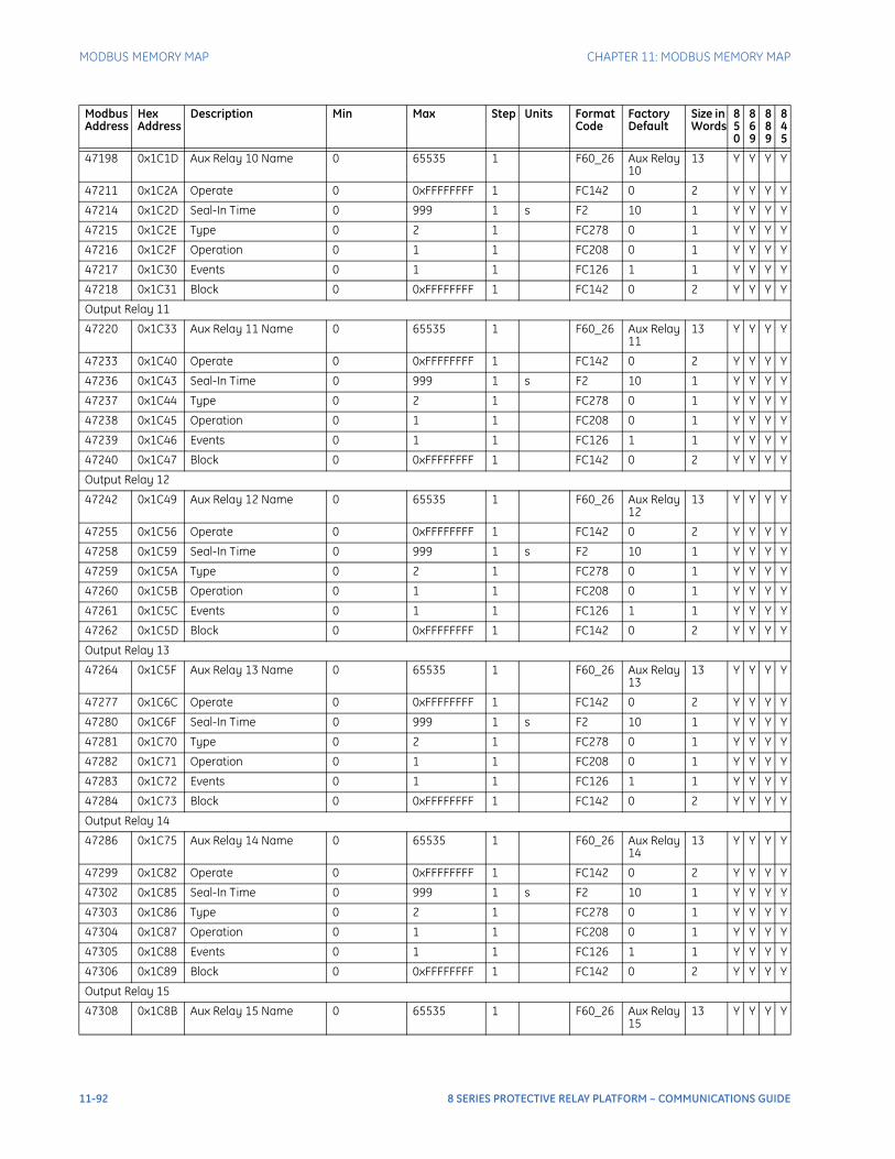
MODBUS MEMORY MAP CHAPTER 11: MODBUS MEMORY MAP
47198 0x1C1D Aux Relay 10 Name 0 65535 1 F60_26 Aux Relay 10
13 Y Y Y Y
47211 0x1C2A Operate 0 0xFFFFFFFF 1 FC142 0 2 Y Y Y Y
47214 0x1C2D Seal-In Time 0 999 1 s F2 10 1 Y Y Y Y
47215 0x1C2E Type 0 2 1 FC278 0 1 Y Y Y Y
47216 0x1C2F Operation 0 1 1 FC208 0 1 Y Y Y Y
47217 0x1C30 Events 0 1 1 FC126 1 1 Y Y Y Y
47218 0x1C31 Block 0 0xFFFFFFFF 1 FC142 0 2 Y Y Y Y
Output Relay 11
47220 0x1C33 Aux Relay 11 Name 0 65535 1 F60_26 Aux Relay 11
13 Y Y Y Y
47233 0x1C40 Operate 0 0xFFFFFFFF 1 FC142 0 2 Y Y Y Y
47236 0x1C43 Seal-In Time 0 999 1 s F2 10 1 Y Y Y Y
47237 0x1C44 Type 0 2 1 FC278 0 1 Y Y Y Y
47238 0x1C45 Operation 0 1 1 FC208 0 1 Y Y Y Y
47239 0x1C46 Events 0 1 1 FC126 1 1 Y Y Y Y
47240 0x1C47 Block 0 0xFFFFFFFF 1 FC142 0 2 Y Y Y Y
Output Relay 12
47242 0x1C49 Aux Relay 12 Name 0 65535 1 F60_26 Aux Relay 12
13 Y Y Y Y
47255 0x1C56 Operate 0 0xFFFFFFFF 1 FC142 0 2 Y Y Y Y
47258 0x1C59 Seal-In Time 0 999 1 s F2 10 1 Y Y Y Y
47259 0x1C5A Type 0 2 1 FC278 0 1 Y Y Y Y
47260 0x1C5B Operation 0 1 1 FC208 0 1 Y Y Y Y
47261 0x1C5C Events 0 1 1 FC126 1 1 Y Y Y Y
47262 0x1C5D Block 0 0xFFFFFFFF 1 FC142 0 2 Y Y Y Y
Output Relay 13
47264 0x1C5F Aux Relay 13 Name 0 65535 1 F60_26 Aux Relay 13
13 Y Y Y Y
47277 0x1C6C Operate 0 0xFFFFFFFF 1 FC142 0 2 Y Y Y Y
47280 0x1C6F Seal-In Time 0 999 1 s F2 10 1 Y Y Y Y
47281 0x1C70 Type 0 2 1 FC278 0 1 Y Y Y Y
47282 0x1C71 Operation 0 1 1 FC208 0 1 Y Y Y Y
47283 0x1C72 Events 0 1 1 FC126 1 1 Y Y Y Y
47284 0x1C73 Block 0 0xFFFFFFFF 1 FC142 0 2 Y Y Y Y
Output Relay 14
47286 0x1C75 Aux Relay 14 Name 0 65535 1 F60_26 Aux Relay 14
13 Y Y Y Y
47299 0x1C82 Operate 0 0xFFFFFFFF 1 FC142 0 2 Y Y Y Y
47302 0x1C85 Seal-In Time 0 999 1 s F2 10 1 Y Y Y Y
47303 0x1C86 Type 0 2 1 FC278 0 1 Y Y Y Y
47304 0x1C87 Operation 0 1 1 FC208 0 1 Y Y Y Y
47305 0x1C88 Events 0 1 1 FC126 1 1 Y Y Y Y
47306 0x1C89 Block 0 0xFFFFFFFF 1 FC142 0 2 Y Y Y Y
Output Relay 15
47308 0x1C8B Aux Relay 15 Name 0 65535 1 F60_26 Aux Relay 15
13 Y Y Y Y
Modbus Address
Hex Address
Description Min Max Step Units Format Code
Factory Default
Size in Words
850
869
889
845
11-92 8 SERIES PROTECTIVE RELAY PLATFORM – COMMUNICATIONS GUIDE
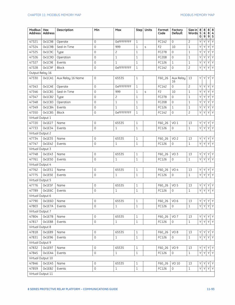
CHAPTER 11: MODBUS MEMORY MAP MODBUS MEMORY MAP
47321 0x1C98 Operate 0 0xFFFFFFFF 1 FC142 0 2 Y Y Y Y
47324 0x1C9B Seal-In Time 0 999 1 s F2 10 1 Y Y Y Y
47325 0x1C9C Type 0 2 1 FC278 0 1 Y Y Y Y
47326 0x1C9D Operation 0 1 1 FC208 0 1 Y Y Y Y
47327 0x1C9E Events 0 1 1 FC126 1 1 Y Y Y Y
47328 0x1C9F Block 0 0xFFFFFFFF 1 FC142 0 2 Y Y Y Y
Output Relay 16
47330 0x1CA1 Aux Relay 16 Name 0 65535 1 F60_26 Aux Relay 16
13 Y Y Y Y
47343 0x1CAE Operate 0 0xFFFFFFFF 1 FC142 0 2 Y Y Y Y
47346 0x1CB1 Seal-In Time 0 999 1 s F2 10 1 Y Y Y Y
47347 0x1CB2 Type 0 2 1 FC278 0 1 Y Y Y Y
47348 0x1CB3 Operation 0 1 1 FC208 0 1 Y Y Y Y
47349 0x1CB4 Events 0 1 1 FC126 1 1 Y Y Y Y
47350 0x1CB5 Block 0 0xFFFFFFFF 1 FC142 0 2 Y Y Y Y
Virtual Output 1
47720 0x1E27 Name 0 65535 1 F60_26 VO 1 13 Y Y Y Y
47733 0x1E34 Events 0 1 1 FC126 0 1 Y Y Y Y
Virtual Output 2
47734 0x1E35 Name 0 65535 1 F60_26 VO 2 13 Y Y Y Y
47747 0x1E42 Events 0 1 1 FC126 0 1 Y Y Y Y
Virtual Output 3
47748 0x1E43 Name 0 65535 1 F60_26 VO 3 13 Y Y Y Y
47761 0x1E50 Events 0 1 1 FC126 0 1 Y Y Y Y
Virtual Output 4
47762 0x1E51 Name 0 65535 1 F60_26 VO 4 13 Y Y Y Y
47775 0x1E5E Events 0 1 1 FC126 0 1 Y Y Y Y
Virtual Output 5
47776 0x1E5F Name 0 65535 1 F60_26 VO 5 13 Y Y Y Y
47789 0x1E6C Events 0 1 1 FC126 0 1 Y Y Y Y
Virtual Output 6
47790 0x1E6D Name 0 65535 1 F60_26 VO 6 13 Y Y Y Y
47803 0x1E7A Events 0 1 1 FC126 0 1 Y Y Y Y
Virtual Output 7
47804 0x1E7B Name 0 65535 1 F60_26 VO 7 13 Y Y Y Y
47817 0x1E88 Events 0 1 1 FC126 0 1 Y Y Y Y
Virtual Output 8
47818 0x1E89 Name 0 65535 1 F60_26 VO 8 13 Y Y Y Y
47831 0x1E96 Events 0 1 1 FC126 0 1 Y Y Y Y
Virtual Output 9
47832 0x1E97 Name 0 65535 1 F60_26 VO 9 13 Y Y Y Y
47845 0x1EA4 Events 0 1 1 FC126 0 1 Y Y Y Y
Virtual Output 10
47846 0x1EA5 Name 0 65535 1 F60_26 VO 10 13 Y Y Y Y
47859 0x1EB2 Events 0 1 1 FC126 0 1 Y Y Y Y
Virtual Output 11
Modbus Address
Hex Address
Description Min Max Step Units Format Code
Factory Default
Size in Words
850
869
889
845
8 SERIES PROTECTIVE RELAY PLATFORM – COMMUNICATIONS GUIDE 11-93

MODBUS MEMORY MAP CHAPTER 11: MODBUS MEMORY MAP
47860 0x1EB3 Name 0 65535 1 F60_26 VO 11 13 Y Y Y Y
47873 0x1EC0 Events 0 1 1 FC126 0 1 Y Y Y Y
Virtual Output 12
47874 0x1EC1 Name 0 65535 1 F60_26 VO 12 13 Y Y Y Y
47887 0x1ECE Events 0 1 1 FC126 0 1 Y Y Y Y
Virtual Output 13
47888 0x1ECF Name 0 65535 1 F60_26 VO 13 13 Y Y Y Y
47901 0x1EDC Events 0 1 1 FC126 0 1 Y Y Y Y
Virtual Output 14
47902 0x1EDD Name 0 65535 1 F60_26 VO 14 13 Y Y Y Y
47915 0x1EEA Events 0 1 1 FC126 0 1 Y Y Y Y
Virtual Output 15
47916 0x1EEB Name 0 65535 1 F60_26 VO 15 13 Y Y Y Y
47929 0x1EF8 Events 0 1 1 FC126 0 1 Y Y Y Y
Virtual Output 16
47930 0x1EF9 Name 0 65535 1 F60_26 VO 16 13 Y Y Y Y
47943 0x1F06 Events 0 1 1 FC126 0 1 Y Y Y Y
Virtual Output 17
47944 0x1F07 Name 0 65535 1 F60_26 VO 17 13 Y Y Y Y
47957 0x1F14 Events 0 1 1 FC126 0 1 Y Y Y Y
Virtual Output 18
47958 0x1F15 Name 0 65535 1 F60_26 VO 18 13 Y Y Y Y
47971 0x1F22 Events 0 1 1 FC126 0 1 Y Y Y Y
Virtual Output 19
47972 0x1F23 Name 0 65535 1 F60_26 VO 19 13 Y Y Y Y
47985 0x1F30 Events 0 1 1 FC126 0 1 Y Y Y Y
Virtual Output 20
47986 0x1F31 Name 0 65535 1 F60_26 VO 20 13 Y Y Y Y
47999 0x1F3E Events 0 1 1 FC126 0 1 Y Y Y Y
Virtual Output 21
48000 0x1F3F Name 0 65535 1 F60_26 VO 21 13 Y Y Y Y
48013 0x1F4C Events 0 1 1 FC126 0 1 Y Y Y Y
Virtual Output 22
48014 0x1F4D Name 0 65535 1 F60_26 VO 22 13 Y Y Y Y
48027 0x1F5A Events 0 1 1 FC126 0 1 Y Y Y Y
Virtual Output 23
48028 0x1F5B Name 0 65535 1 F60_26 VO 23 13 Y Y Y Y
48041 0x1F68 Events 0 1 1 FC126 0 1 Y Y Y Y
Virtual Output 24
48042 0x1F69 Name 0 65535 1 F60_26 VO 24 13 Y Y Y Y
48055 0x1F76 Events 0 1 1 FC126 0 1 Y Y Y Y
Virtual Output 25
48056 0x1F77 Name 0 65535 1 F60_26 VO 25 13 Y Y Y Y
48069 0x1F84 Events 0 1 1 FC126 0 1 Y Y Y Y
Virtual Output 26
Modbus Address
Hex Address
Description Min Max Step Units Format Code
Factory Default
Size in Words
850
869
889
845
11-94 8 SERIES PROTECTIVE RELAY PLATFORM – COMMUNICATIONS GUIDE
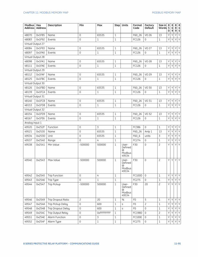
CHAPTER 11: MODBUS MEMORY MAP MODBUS MEMORY MAP
48070 0x1F85 Name 0 65535 1 F60_26 VO 26 13 Y Y Y Y
48083 0x1F92 Events 0 1 1 FC126 0 1 Y Y Y Y
Virtual Output 27
48084 0x1F93 Name 0 65535 1 F60_26 VO 27 13 Y Y Y Y
48097 0x1FA0 Events 0 1 1 FC126 0 1 Y Y Y Y
Virtual Output 28
48098 0x1FA1 Name 0 65535 1 F60_26 VO 28 13 Y Y Y Y
48111 0x1FAE Events 0 1 1 FC126 0 1 Y Y Y Y
Virtual Output 29
48112 0x1FAF Name 0 65535 1 F60_26 VO 29 13 Y Y Y Y
48125 0x1FBC Events 0 1 1 FC126 0 1 Y Y Y Y
Virtual Output 30
48126 0x1FBD Name 0 65535 1 F60_26 VO 30 13 Y Y Y Y
48139 0x1FCA Events 0 1 1 FC126 0 1 Y Y Y Y
Virtual Output 31
48140 0x1FCB Name 0 65535 1 F60_26 VO 31 13 Y Y Y Y
48153 0x1FD8 Events 0 1 1 FC126 0 1 Y Y Y Y
Virtual Output 32
48154 0x1FD9 Name 0 65535 1 F60_26 VO 32 13 Y Y Y Y
48167 0x1FE6 Events 0 1 1 FC126 0 1 Y Y Y Y
Analog Input 1
49520 0x252F Function 0 3 1 FC386 0 1 Y Y Y Y
49521 0x2530 Name 0 65535 1 F60_26 AnIp 1 13 Y Y Y Y
49534 0x253D Unit 0 65535 1 F60_6 units 3 Y Y Y Y
49537 0x2540 Range 0 4 1 FC274 0 1 Y Y Y Y
49538 0x2541 Min Value -500000 500000 1 User-Defined @ Modbus 49534
F30 0 2 Y Y Y Y
49540 0x2543 Max Value -500000 500000 1 User-Defined @ Modbus 49534
F30 0 2 Y Y Y Y
49542 0x2545 Trip Function 0 4 1 FC100D 0 1 Y Y Y Y
49543 0x2546 Trip Type 0 1 1 FC275 0 1 Y Y Y Y
49544 0x2547 Trip Pickup -500000 500000 1 User-Defined @ Modbus 49534
F30 20 2 Y Y Y Y
49546 0x2549 Trip Dropout Ratio 2 20 1 % F0 5 1 Y Y Y Y
49547 0x254A Trip Pickup Delay 0 600 1 s F0 2 1 Y Y Y Y
49548 0x254B Trip Dropout Delay 0 600 1 s F0 0 1 Y Y Y Y
49549 0x254C Trip Output Relay 0 0xFFFFFFFF 1 FC198D 0 2 Y Y Y Y
49551 0x254E Alarm Function 0 3 1 FC100E 0 1 Y Y Y Y
49552 0x254F Alarm Type 0 1 1 FC275 0 1 Y Y Y Y
Modbus Address
Hex Address
Description Min Max Step Units Format Code
Factory Default
Size in Words
850
869
889
845
8 SERIES PROTECTIVE RELAY PLATFORM – COMMUNICATIONS GUIDE 11-95
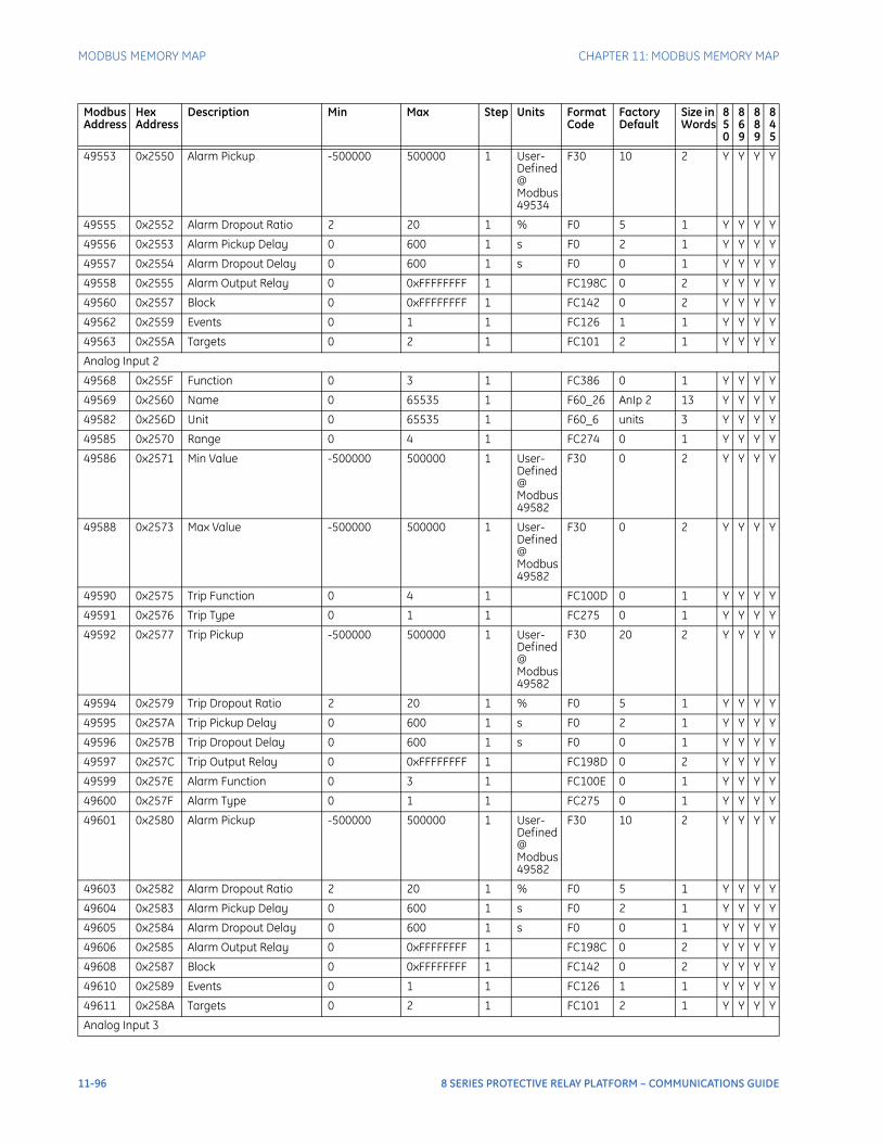
MODBUS MEMORY MAP CHAPTER 11: MODBUS MEMORY MAP
49553 0x2550 Alarm Pickup -500000 500000 1 User-Defined @ Modbus 49534
F30 10 2 Y Y Y Y
49555 0x2552 Alarm Dropout Ratio 2 20 1 % F0 5 1 Y Y Y Y
49556 0x2553 Alarm Pickup Delay 0 600 1 s F0 2 1 Y Y Y Y
49557 0x2554 Alarm Dropout Delay 0 600 1 s F0 0 1 Y Y Y Y
49558 0x2555 Alarm Output Relay 0 0xFFFFFFFF 1 FC198C 0 2 Y Y Y Y
49560 0x2557 Block 0 0xFFFFFFFF 1 FC142 0 2 Y Y Y Y
49562 0x2559 Events 0 1 1 FC126 1 1 Y Y Y Y
49563 0x255A Targets 0 2 1 FC101 2 1 Y Y Y Y
Analog Input 2
49568 0x255F Function 0 3 1 FC386 0 1 Y Y Y Y
49569 0x2560 Name 0 65535 1 F60_26 AnIp 2 13 Y Y Y Y
49582 0x256D Unit 0 65535 1 F60_6 units 3 Y Y Y Y
49585 0x2570 Range 0 4 1 FC274 0 1 Y Y Y Y
49586 0x2571 Min Value -500000 500000 1 User-Defined @ Modbus 49582
F30 0 2 Y Y Y Y
49588 0x2573 Max Value -500000 500000 1 User-Defined @ Modbus 49582
F30 0 2 Y Y Y Y
49590 0x2575 Trip Function 0 4 1 FC100D 0 1 Y Y Y Y
49591 0x2576 Trip Type 0 1 1 FC275 0 1 Y Y Y Y
49592 0x2577 Trip Pickup -500000 500000 1 User-Defined @ Modbus 49582
F30 20 2 Y Y Y Y
49594 0x2579 Trip Dropout Ratio 2 20 1 % F0 5 1 Y Y Y Y
49595 0x257A Trip Pickup Delay 0 600 1 s F0 2 1 Y Y Y Y
49596 0x257B Trip Dropout Delay 0 600 1 s F0 0 1 Y Y Y Y
49597 0x257C Trip Output Relay 0 0xFFFFFFFF 1 FC198D 0 2 Y Y Y Y
49599 0x257E Alarm Function 0 3 1 FC100E 0 1 Y Y Y Y
49600 0x257F Alarm Type 0 1 1 FC275 0 1 Y Y Y Y
49601 0x2580 Alarm Pickup -500000 500000 1 User-Defined @ Modbus 49582
F30 10 2 Y Y Y Y
49603 0x2582 Alarm Dropout Ratio 2 20 1 % F0 5 1 Y Y Y Y
49604 0x2583 Alarm Pickup Delay 0 600 1 s F0 2 1 Y Y Y Y
49605 0x2584 Alarm Dropout Delay 0 600 1 s F0 0 1 Y Y Y Y
49606 0x2585 Alarm Output Relay 0 0xFFFFFFFF 1 FC198C 0 2 Y Y Y Y
49608 0x2587 Block 0 0xFFFFFFFF 1 FC142 0 2 Y Y Y Y
49610 0x2589 Events 0 1 1 FC126 1 1 Y Y Y Y
49611 0x258A Targets 0 2 1 FC101 2 1 Y Y Y Y
Analog Input 3
Modbus Address
Hex Address
Description Min Max Step Units Format Code
Factory Default
Size in Words
850
869
889
845
11-96 8 SERIES PROTECTIVE RELAY PLATFORM – COMMUNICATIONS GUIDE
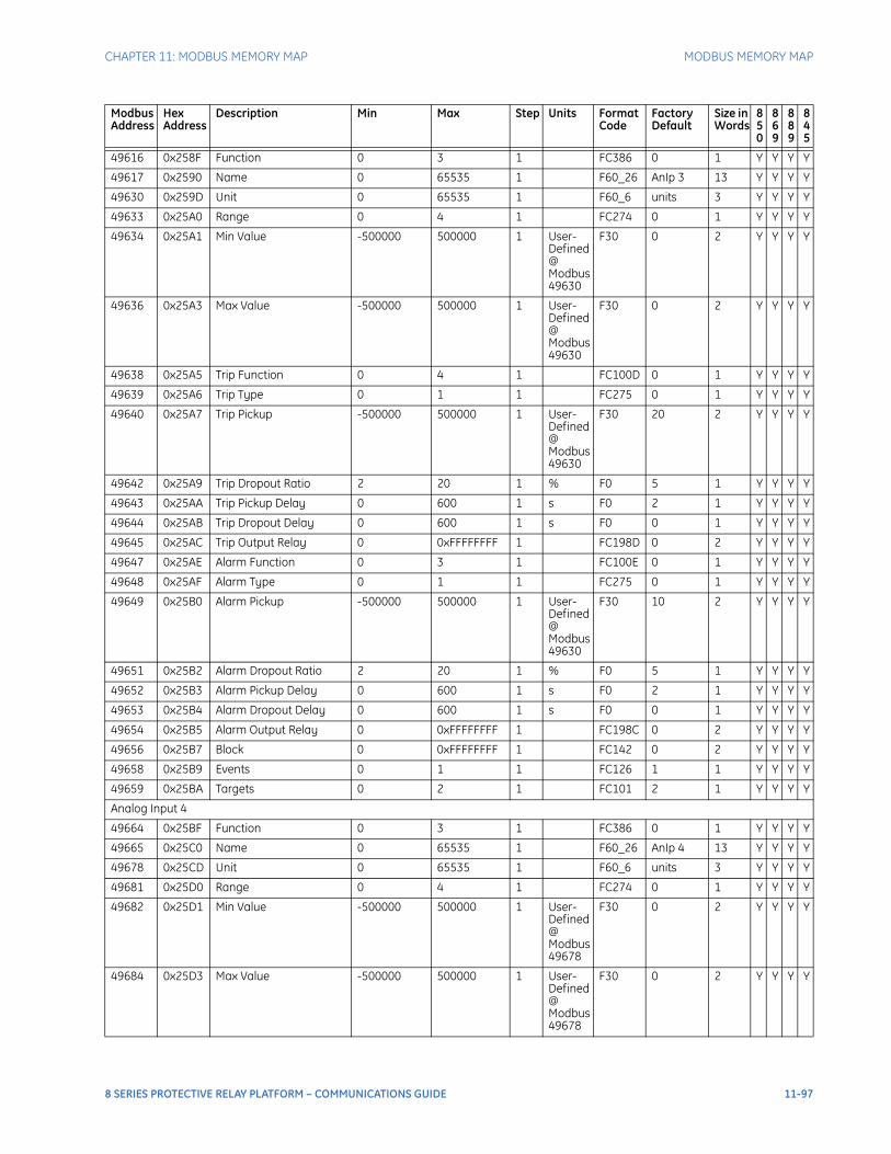
CHAPTER 11: MODBUS MEMORY MAP MODBUS MEMORY MAP
49616 0x258F Function 0 3 1 FC386 0 1 Y Y Y Y
49617 0x2590 Name 0 65535 1 F60_26 AnIp 3 13 Y Y Y Y
49630 0x259D Unit 0 65535 1 F60_6 units 3 Y Y Y Y
49633 0x25A0 Range 0 4 1 FC274 0 1 Y Y Y Y
49634 0x25A1 Min Value -500000 500000 1 User-Defined @ Modbus 49630
F30 0 2 Y Y Y Y
49636 0x25A3 Max Value -500000 500000 1 User-Defined @ Modbus 49630
F30 0 2 Y Y Y Y
49638 0x25A5 Trip Function 0 4 1 FC100D 0 1 Y Y Y Y
49639 0x25A6 Trip Type 0 1 1 FC275 0 1 Y Y Y Y
49640 0x25A7 Trip Pickup -500000 500000 1 User-Defined @ Modbus 49630
F30 20 2 Y Y Y Y
49642 0x25A9 Trip Dropout Ratio 2 20 1 % F0 5 1 Y Y Y Y
49643 0x25AA Trip Pickup Delay 0 600 1 s F0 2 1 Y Y Y Y
49644 0x25AB Trip Dropout Delay 0 600 1 s F0 0 1 Y Y Y Y
49645 0x25AC Trip Output Relay 0 0xFFFFFFFF 1 FC198D 0 2 Y Y Y Y
49647 0x25AE Alarm Function 0 3 1 FC100E 0 1 Y Y Y Y
49648 0x25AF Alarm Type 0 1 1 FC275 0 1 Y Y Y Y
49649 0x25B0 Alarm Pickup -500000 500000 1 User-Defined @ Modbus 49630
F30 10 2 Y Y Y Y
49651 0x25B2 Alarm Dropout Ratio 2 20 1 % F0 5 1 Y Y Y Y
49652 0x25B3 Alarm Pickup Delay 0 600 1 s F0 2 1 Y Y Y Y
49653 0x25B4 Alarm Dropout Delay 0 600 1 s F0 0 1 Y Y Y Y
49654 0x25B5 Alarm Output Relay 0 0xFFFFFFFF 1 FC198C 0 2 Y Y Y Y
49656 0x25B7 Block 0 0xFFFFFFFF 1 FC142 0 2 Y Y Y Y
49658 0x25B9 Events 0 1 1 FC126 1 1 Y Y Y Y
49659 0x25BA Targets 0 2 1 FC101 2 1 Y Y Y Y
Analog Input 4
49664 0x25BF Function 0 3 1 FC386 0 1 Y Y Y Y
49665 0x25C0 Name 0 65535 1 F60_26 AnIp 4 13 Y Y Y Y
49678 0x25CD Unit 0 65535 1 F60_6 units 3 Y Y Y Y
49681 0x25D0 Range 0 4 1 FC274 0 1 Y Y Y Y
49682 0x25D1 Min Value -500000 500000 1 User-Defined @ Modbus 49678
F30 0 2 Y Y Y Y
49684 0x25D3 Max Value -500000 500000 1 User-Defined @ Modbus 49678
F30 0 2 Y Y Y Y
Modbus Address
Hex Address
Description Min Max Step Units Format Code
Factory Default
Size in Words
850
869
889
845
8 SERIES PROTECTIVE RELAY PLATFORM – COMMUNICATIONS GUIDE 11-97
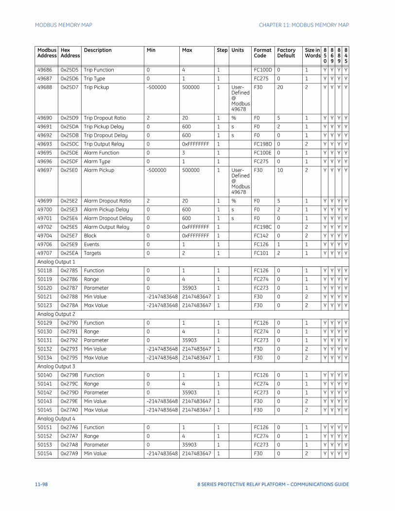
MODBUS MEMORY MAP CHAPTER 11: MODBUS MEMORY MAP
49686 0x25D5 Trip Function 0 4 1 FC100D 0 1 Y Y Y Y
49687 0x25D6 Trip Type 0 1 1 FC275 0 1 Y Y Y Y
49688 0x25D7 Trip Pickup -500000 500000 1 User-Defined @ Modbus 49678
F30 20 2 Y Y Y Y
49690 0x25D9 Trip Dropout Ratio 2 20 1 % F0 5 1 Y Y Y Y
49691 0x25DA Trip Pickup Delay 0 600 1 s F0 2 1 Y Y Y Y
49692 0x25DB Trip Dropout Delay 0 600 1 s F0 0 1 Y Y Y Y
49693 0x25DC Trip Output Relay 0 0xFFFFFFFF 1 FC198D 0 2 Y Y Y Y
49695 0x25DE Alarm Function 0 3 1 FC100E 0 1 Y Y Y Y
49696 0x25DF Alarm Type 0 1 1 FC275 0 1 Y Y Y Y
49697 0x25E0 Alarm Pickup -500000 500000 1 User-Defined @ Modbus 49678
F30 10 2 Y Y Y Y
49699 0x25E2 Alarm Dropout Ratio 2 20 1 % F0 5 1 Y Y Y Y
49700 0x25E3 Alarm Pickup Delay 0 600 1 s F0 2 1 Y Y Y Y
49701 0x25E4 Alarm Dropout Delay 0 600 1 s F0 0 1 Y Y Y Y
49702 0x25E5 Alarm Output Relay 0 0xFFFFFFFF 1 FC198C 0 2 Y Y Y Y
49704 0x25E7 Block 0 0xFFFFFFFF 1 FC142 0 2 Y Y Y Y
49706 0x25E9 Events 0 1 1 FC126 1 1 Y Y Y Y
49707 0x25EA Targets 0 2 1 FC101 2 1 Y Y Y Y
Analog Output 1
50118 0x2785 Function 0 1 1 FC126 0 1 Y Y Y Y
50119 0x2786 Range 0 4 1 FC274 0 1 Y Y Y Y
50120 0x2787 Parameter 0 35903 1 FC273 0 1 Y Y Y Y
50121 0x2788 Min Value -2147483648 2147483647 1 F30 0 2 Y Y Y Y
50123 0x278A Max Value -2147483648 2147483647 1 F30 0 2 Y Y Y Y
Analog Output 2
50129 0x2790 Function 0 1 1 FC126 0 1 Y Y Y Y
50130 0x2791 Range 0 4 1 FC274 0 1 Y Y Y Y
50131 0x2792 Parameter 0 35903 1 FC273 0 1 Y Y Y Y
50132 0x2793 Min Value -2147483648 2147483647 1 F30 0 2 Y Y Y Y
50134 0x2795 Max Value -2147483648 2147483647 1 F30 0 2 Y Y Y Y
Analog Output 3
50140 0x279B Function 0 1 1 FC126 0 1 Y Y Y Y
50141 0x279C Range 0 4 1 FC274 0 1 Y Y Y Y
50142 0x279D Parameter 0 35903 1 FC273 0 1 Y Y Y Y
50143 0x279E Min Value -2147483648 2147483647 1 F30 0 2 Y Y Y Y
50145 0x27A0 Max Value -2147483648 2147483647 1 F30 0 2 Y Y Y Y
Analog Output 4
50151 0x27A6 Function 0 1 1 FC126 0 1 Y Y Y Y
50152 0x27A7 Range 0 4 1 FC274 0 1 Y Y Y Y
50153 0x27A8 Parameter 0 35903 1 FC273 0 1 Y Y Y Y
50154 0x27A9 Min Value -2147483648 2147483647 1 F30 0 2 Y Y Y Y
Modbus Address
Hex Address
Description Min Max Step Units Format Code
Factory Default
Size in Words
850
869
889
845
11-98 8 SERIES PROTECTIVE RELAY PLATFORM – COMMUNICATIONS GUIDE
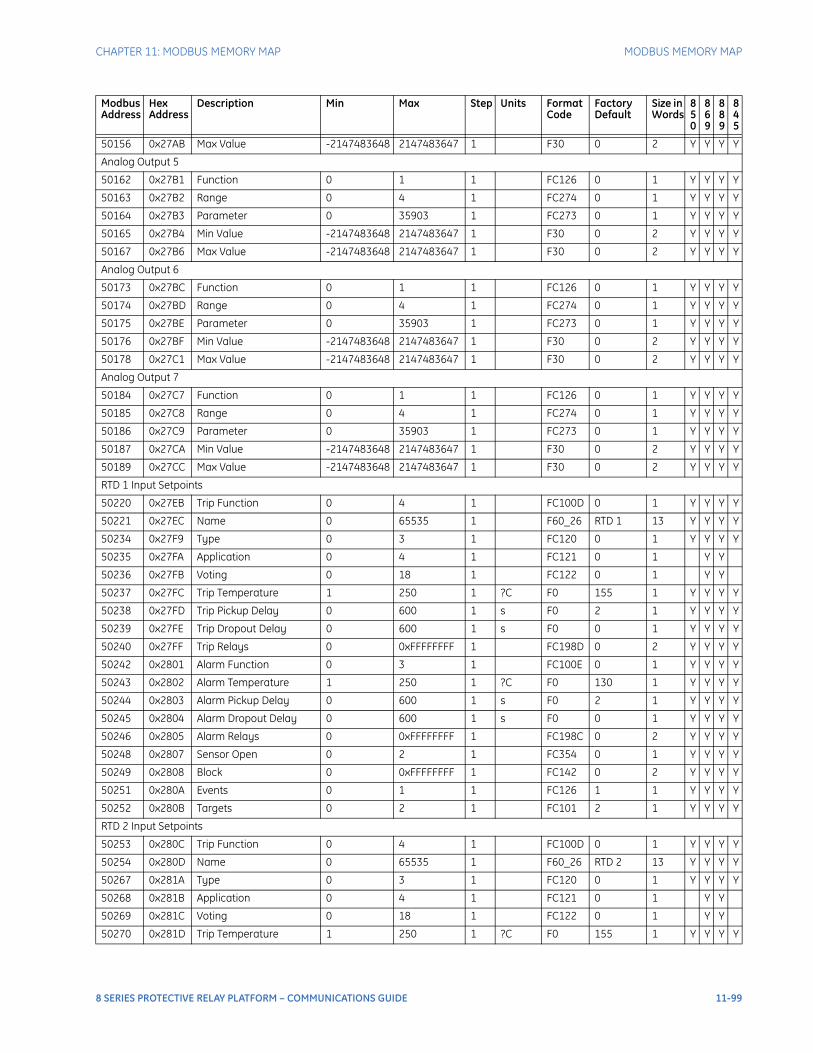
CHAPTER 11: MODBUS MEMORY MAP MODBUS MEMORY MAP
50156 0x27AB Max Value -2147483648 2147483647 1 F30 0 2 Y Y Y Y
Analog Output 5
50162 0x27B1 Function 0 1 1 FC126 0 1 Y Y Y Y
50163 0x27B2 Range 0 4 1 FC274 0 1 Y Y Y Y
50164 0x27B3 Parameter 0 35903 1 FC273 0 1 Y Y Y Y
50165 0x27B4 Min Value -2147483648 2147483647 1 F30 0 2 Y Y Y Y
50167 0x27B6 Max Value -2147483648 2147483647 1 F30 0 2 Y Y Y Y
Analog Output 6
50173 0x27BC Function 0 1 1 FC126 0 1 Y Y Y Y
50174 0x27BD Range 0 4 1 FC274 0 1 Y Y Y Y
50175 0x27BE Parameter 0 35903 1 FC273 0 1 Y Y Y Y
50176 0x27BF Min Value -2147483648 2147483647 1 F30 0 2 Y Y Y Y
50178 0x27C1 Max Value -2147483648 2147483647 1 F30 0 2 Y Y Y Y
Analog Output 7
50184 0x27C7 Function 0 1 1 FC126 0 1 Y Y Y Y
50185 0x27C8 Range 0 4 1 FC274 0 1 Y Y Y Y
50186 0x27C9 Parameter 0 35903 1 FC273 0 1 Y Y Y Y
50187 0x27CA Min Value -2147483648 2147483647 1 F30 0 2 Y Y Y Y
50189 0x27CC Max Value -2147483648 2147483647 1 F30 0 2 Y Y Y Y
RTD 1 Input Setpoints
50220 0x27EB Trip Function 0 4 1 FC100D 0 1 Y Y Y Y
50221 0x27EC Name 0 65535 1 F60_26 RTD 1 13 Y Y Y Y
50234 0x27F9 Type 0 3 1 FC120 0 1 Y Y Y Y
50235 0x27FA Application 0 4 1 FC121 0 1 Y Y
50236 0x27FB Voting 0 18 1 FC122 0 1 Y Y
50237 0x27FC Trip Temperature 1 250 1 ?C F0 155 1 Y Y Y Y
50238 0x27FD Trip Pickup Delay 0 600 1 s F0 2 1 Y Y Y Y
50239 0x27FE Trip Dropout Delay 0 600 1 s F0 0 1 Y Y Y Y
50240 0x27FF Trip Relays 0 0xFFFFFFFF 1 FC198D 0 2 Y Y Y Y
50242 0x2801 Alarm Function 0 3 1 FC100E 0 1 Y Y Y Y
50243 0x2802 Alarm Temperature 1 250 1 ?C F0 130 1 Y Y Y Y
50244 0x2803 Alarm Pickup Delay 0 600 1 s F0 2 1 Y Y Y Y
50245 0x2804 Alarm Dropout Delay 0 600 1 s F0 0 1 Y Y Y Y
50246 0x2805 Alarm Relays 0 0xFFFFFFFF 1 FC198C 0 2 Y Y Y Y
50248 0x2807 Sensor Open 0 2 1 FC354 0 1 Y Y Y Y
50249 0x2808 Block 0 0xFFFFFFFF 1 FC142 0 2 Y Y Y Y
50251 0x280A Events 0 1 1 FC126 1 1 Y Y Y Y
50252 0x280B Targets 0 2 1 FC101 2 1 Y Y Y Y
RTD 2 Input Setpoints
50253 0x280C Trip Function 0 4 1 FC100D 0 1 Y Y Y Y
50254 0x280D Name 0 65535 1 F60_26 RTD 2 13 Y Y Y Y
50267 0x281A Type 0 3 1 FC120 0 1 Y Y Y Y
50268 0x281B Application 0 4 1 FC121 0 1 Y Y
50269 0x281C Voting 0 18 1 FC122 0 1 Y Y
50270 0x281D Trip Temperature 1 250 1 ?C F0 155 1 Y Y Y Y
Modbus Address
Hex Address
Description Min Max Step Units Format Code
Factory Default
Size in Words
850
869
889
845
8 SERIES PROTECTIVE RELAY PLATFORM – COMMUNICATIONS GUIDE 11-99
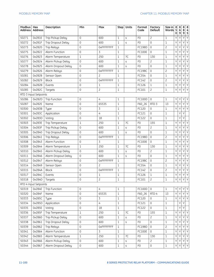
MODBUS MEMORY MAP CHAPTER 11: MODBUS MEMORY MAP
50271 0x281E Trip Pickup Delay 0 600 1 s F0 2 1 Y Y Y Y
50272 0x281F Trip Dropout Delay 0 600 1 s F0 0 1 Y Y Y Y
50273 0x2820 Trip Relays 0 0xFFFFFFFF 1 FC198D 0 2 Y Y Y Y
50275 0x2822 Alarm Function 0 3 1 FC100E 0 1 Y Y Y Y
50276 0x2823 Alarm Temperature 1 250 1 ?C F0 130 1 Y Y Y Y
50277 0x2824 Alarm Pickup Delay 0 600 1 s F0 2 1 Y Y Y Y
50278 0x2825 Alarm Dropout Delay 0 600 1 s F0 0 1 Y Y Y Y
50279 0x2826 Alarm Relays 0 0xFFFFFFFF 1 FC198C 0 2 Y Y Y Y
50281 0x2828 Sensor Open 0 2 1 FC354 0 1 Y Y Y Y
50282 0x2829 Block 0 0xFFFFFFFF 1 FC142 0 2 Y Y Y Y
50284 0x282B Events 0 1 1 FC126 1 1 Y Y Y Y
50285 0x282C Targets 0 2 1 FC101 2 1 Y Y Y Y
RTD 3 Input Setpoints
50286 0x282D Trip Function 0 4 1 FC100D 0 1 Y Y Y Y
50287 0x282E Name 0 65535 1 F60_26 RTD 3 13 Y Y Y Y
50300 0x283B Type 0 3 1 FC120 0 1 Y Y Y Y
50301 0x283C Application 0 4 1 FC121 0 1 Y Y
50302 0x283D Voting 0 18 1 FC122 0 1 Y Y
50303 0x283E Trip Temperature 1 250 1 ?C F0 155 1 Y Y Y Y
50304 0x283F Trip Pickup Delay 0 600 1 s F0 2 1 Y Y Y Y
50305 0x2840 Trip Dropout Delay 0 600 1 s F0 0 1 Y Y Y Y
50306 0x2841 Trip Relays 0 0xFFFFFFFF 1 FC198D 0 2 Y Y Y Y
50308 0x2843 Alarm Function 0 3 1 FC100E 0 1 Y Y Y Y
50309 0x2844 Alarm Temperature 1 250 1 ?C F0 130 1 Y Y Y Y
50310 0x2845 Alarm Pickup Delay 0 600 1 s F0 2 1 Y Y Y Y
50311 0x2846 Alarm Dropout Delay 0 600 1 s F0 0 1 Y Y Y Y
50312 0x2847 Alarm Relays 0 0xFFFFFFFF 1 FC198C 0 2 Y Y Y Y
50314 0x2849 Sensor Open 0 2 1 FC354 0 1 Y Y Y Y
50315 0x284A Block 0 0xFFFFFFFF 1 FC142 0 2 Y Y Y Y
50317 0x284C Events 0 1 1 FC126 1 1 Y Y Y Y
50318 0x284D Targets 0 2 1 FC101 2 1 Y Y Y Y
RTD 4 Input Setpoints
50319 0x284E Trip Function 0 4 1 FC100D 0 1 Y Y Y Y
50320 0x284F Name 0 65535 1 F60_26 RTD 4 13 Y Y Y Y
50333 0x285C Type 0 3 1 FC120 0 1 Y Y Y Y
50334 0x285D Application 0 4 1 FC121 0 1 Y Y
50335 0x285E Voting 0 18 1 FC122 0 1 Y Y
50336 0x285F Trip Temperature 1 250 1 ?C F0 155 1 Y Y Y Y
50337 0x2860 Trip Pickup Delay 0 600 1 s F0 2 1 Y Y Y Y
50338 0x2861 Trip Dropout Delay 0 600 1 s F0 0 1 Y Y Y Y
50339 0x2862 Trip Relays 0 0xFFFFFFFF 1 FC198D 0 2 Y Y Y Y
50341 0x2864 Alarm Function 0 3 1 FC100E 0 1 Y Y Y Y
50342 0x2865 Alarm Temperature 1 250 1 ?C F0 130 1 Y Y Y Y
50343 0x2866 Alarm Pickup Delay 0 600 1 s F0 2 1 Y Y Y Y
50344 0x2867 Alarm Dropout Delay 0 600 1 s F0 0 1 Y Y Y Y
Modbus Address
Hex Address
Description Min Max Step Units Format Code
Factory Default
Size in Words
850
869
889
845
11-100 8 SERIES PROTECTIVE RELAY PLATFORM – COMMUNICATIONS GUIDE

CHAPTER 11: MODBUS MEMORY MAP MODBUS MEMORY MAP
50345 0x2868 Alarm Relays 0 0xFFFFFFFF 1 FC198C 0 2 Y Y Y Y
50347 0x286A Sensor Open 0 2 1 FC354 0 1 Y Y Y Y
50348 0x286B Block 0 0xFFFFFFFF 1 FC142 0 2 Y Y Y Y
50350 0x286D Events 0 1 1 FC126 1 1 Y Y Y Y
50351 0x286E Targets 0 2 1 FC101 2 1 Y Y Y Y
RTD 5 Input Setpoints
50352 0x286F Trip Function 0 4 1 FC100D 0 1 Y Y Y Y
50353 0x2870 Name 0 65535 1 F60_26 RTD 5 13 Y Y Y Y
50366 0x287D Type 0 3 1 FC120 0 1 Y Y Y Y
50367 0x287E Application 0 4 1 FC121 0 1 Y Y
50368 0x287F Voting 0 18 1 FC122 0 1 Y Y
50369 0x2880 Trip Temperature 1 250 1 ?C F0 155 1 Y Y Y Y
50370 0x2881 Trip Pickup Delay 0 600 1 s F0 2 1 Y Y Y Y
50371 0x2882 Trip Dropout Delay 0 600 1 s F0 0 1 Y Y Y Y
50372 0x2883 Trip Relays 0 0xFFFFFFFF 1 FC198D 0 2 Y Y Y Y
50374 0x2885 Alarm Function 0 3 1 FC100E 0 1 Y Y Y Y
50375 0x2886 Alarm Temperature 1 250 1 ?C F0 130 1 Y Y Y Y
50376 0x2887 Alarm Pickup Delay 0 600 1 s F0 2 1 Y Y Y Y
50377 0x2888 Alarm Dropout Delay 0 600 1 s F0 0 1 Y Y Y Y
50378 0x2889 Alarm Relays 0 0xFFFFFFFF 1 FC198C 0 2 Y Y Y Y
50380 0x288B Sensor Open 0 2 1 FC354 0 1 Y Y Y Y
50381 0x288C Block 0 0xFFFFFFFF 1 FC142 0 2 Y Y Y Y
50383 0x288E Events 0 1 1 FC126 1 1 Y Y Y Y
50384 0x288F Targets 0 2 1 FC101 2 1 Y Y Y Y
RTD 6 Input Setpoints
50385 0x2890 Trip Function 0 4 1 FC100D 0 1 Y Y Y Y
50386 0x2891 Name 0 65535 1 F60_26 RTD 6 13 Y Y Y Y
50399 0x289E Type 0 3 1 FC120 0 1 Y Y Y Y
50400 0x289F Application 0 4 1 FC121 0 1 Y Y
50401 0x28A0 Voting 0 18 1 FC122 0 1 Y Y
50402 0x28A1 Trip Temperature 1 250 1 ?C F0 155 1 Y Y Y Y
50403 0x28A2 Trip Pickup Delay 0 600 1 s F0 2 1 Y Y Y Y
50404 0x28A3 Trip Dropout Delay 0 600 1 s F0 0 1 Y Y Y Y
50405 0x28A4 Trip Relays 0 0xFFFFFFFF 1 FC198D 0 2 Y Y Y Y
50407 0x28A6 Alarm Function 0 3 1 FC100E 0 1 Y Y Y Y
50408 0x28A7 Alarm Temperature 1 250 1 ?C F0 130 1 Y Y Y Y
50409 0x28A8 Alarm Pickup Delay 0 600 1 s F0 2 1 Y Y Y Y
50410 0x28A9 Alarm Dropout Delay 0 600 1 s F0 0 1 Y Y Y Y
50411 0x28AA Alarm Relays 0 0xFFFFFFFF 1 FC198C 0 2 Y Y Y Y
50413 0x28AC Sensor Open 0 2 1 FC354 0 1 Y Y Y Y
50414 0x28AD Block 0 0xFFFFFFFF 1 FC142 0 2 Y Y Y Y
50416 0x28AF Events 0 1 1 FC126 1 1 Y Y Y Y
50417 0x28B0 Targets 0 2 1 FC101 2 1 Y Y Y Y
RTD 7 Input Setpoints
50418 0x28B1 Trip Function 0 4 1 FC100D 0 1 Y Y Y Y
Modbus Address
Hex Address
Description Min Max Step Units Format Code
Factory Default
Size in Words
850
869
889
845
8 SERIES PROTECTIVE RELAY PLATFORM – COMMUNICATIONS GUIDE 11-101
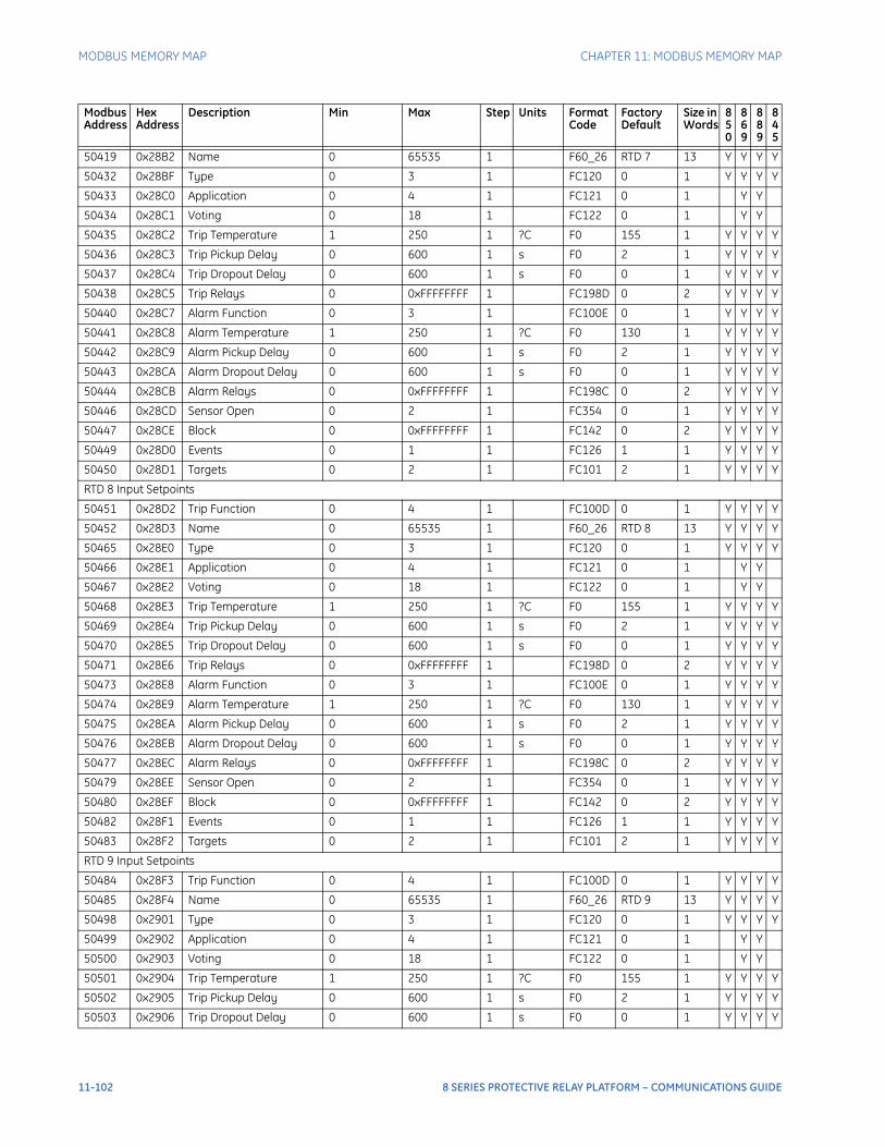
MODBUS MEMORY MAP CHAPTER 11: MODBUS MEMORY MAP
50419 0x28B2 Name 0 65535 1 F60_26 RTD 7 13 Y Y Y Y
50432 0x28BF Type 0 3 1 FC120 0 1 Y Y Y Y
50433 0x28C0 Application 0 4 1 FC121 0 1 Y Y
50434 0x28C1 Voting 0 18 1 FC122 0 1 Y Y
50435 0x28C2 Trip Temperature 1 250 1 ?C F0 155 1 Y Y Y Y
50436 0x28C3 Trip Pickup Delay 0 600 1 s F0 2 1 Y Y Y Y
50437 0x28C4 Trip Dropout Delay 0 600 1 s F0 0 1 Y Y Y Y
50438 0x28C5 Trip Relays 0 0xFFFFFFFF 1 FC198D 0 2 Y Y Y Y
50440 0x28C7 Alarm Function 0 3 1 FC100E 0 1 Y Y Y Y
50441 0x28C8 Alarm Temperature 1 250 1 ?C F0 130 1 Y Y Y Y
50442 0x28C9 Alarm Pickup Delay 0 600 1 s F0 2 1 Y Y Y Y
50443 0x28CA Alarm Dropout Delay 0 600 1 s F0 0 1 Y Y Y Y
50444 0x28CB Alarm Relays 0 0xFFFFFFFF 1 FC198C 0 2 Y Y Y Y
50446 0x28CD Sensor Open 0 2 1 FC354 0 1 Y Y Y Y
50447 0x28CE Block 0 0xFFFFFFFF 1 FC142 0 2 Y Y Y Y
50449 0x28D0 Events 0 1 1 FC126 1 1 Y Y Y Y
50450 0x28D1 Targets 0 2 1 FC101 2 1 Y Y Y Y
RTD 8 Input Setpoints
50451 0x28D2 Trip Function 0 4 1 FC100D 0 1 Y Y Y Y
50452 0x28D3 Name 0 65535 1 F60_26 RTD 8 13 Y Y Y Y
50465 0x28E0 Type 0 3 1 FC120 0 1 Y Y Y Y
50466 0x28E1 Application 0 4 1 FC121 0 1 Y Y
50467 0x28E2 Voting 0 18 1 FC122 0 1 Y Y
50468 0x28E3 Trip Temperature 1 250 1 ?C F0 155 1 Y Y Y Y
50469 0x28E4 Trip Pickup Delay 0 600 1 s F0 2 1 Y Y Y Y
50470 0x28E5 Trip Dropout Delay 0 600 1 s F0 0 1 Y Y Y Y
50471 0x28E6 Trip Relays 0 0xFFFFFFFF 1 FC198D 0 2 Y Y Y Y
50473 0x28E8 Alarm Function 0 3 1 FC100E 0 1 Y Y Y Y
50474 0x28E9 Alarm Temperature 1 250 1 ?C F0 130 1 Y Y Y Y
50475 0x28EA Alarm Pickup Delay 0 600 1 s F0 2 1 Y Y Y Y
50476 0x28EB Alarm Dropout Delay 0 600 1 s F0 0 1 Y Y Y Y
50477 0x28EC Alarm Relays 0 0xFFFFFFFF 1 FC198C 0 2 Y Y Y Y
50479 0x28EE Sensor Open 0 2 1 FC354 0 1 Y Y Y Y
50480 0x28EF Block 0 0xFFFFFFFF 1 FC142 0 2 Y Y Y Y
50482 0x28F1 Events 0 1 1 FC126 1 1 Y Y Y Y
50483 0x28F2 Targets 0 2 1 FC101 2 1 Y Y Y Y
RTD 9 Input Setpoints
50484 0x28F3 Trip Function 0 4 1 FC100D 0 1 Y Y Y Y
50485 0x28F4 Name 0 65535 1 F60_26 RTD 9 13 Y Y Y Y
50498 0x2901 Type 0 3 1 FC120 0 1 Y Y Y Y
50499 0x2902 Application 0 4 1 FC121 0 1 Y Y
50500 0x2903 Voting 0 18 1 FC122 0 1 Y Y
50501 0x2904 Trip Temperature 1 250 1 ?C F0 155 1 Y Y Y Y
50502 0x2905 Trip Pickup Delay 0 600 1 s F0 2 1 Y Y Y Y
50503 0x2906 Trip Dropout Delay 0 600 1 s F0 0 1 Y Y Y Y
Modbus Address
Hex Address
Description Min Max Step Units Format Code
Factory Default
Size in Words
850
869
889
845
11-102 8 SERIES PROTECTIVE RELAY PLATFORM – COMMUNICATIONS GUIDE
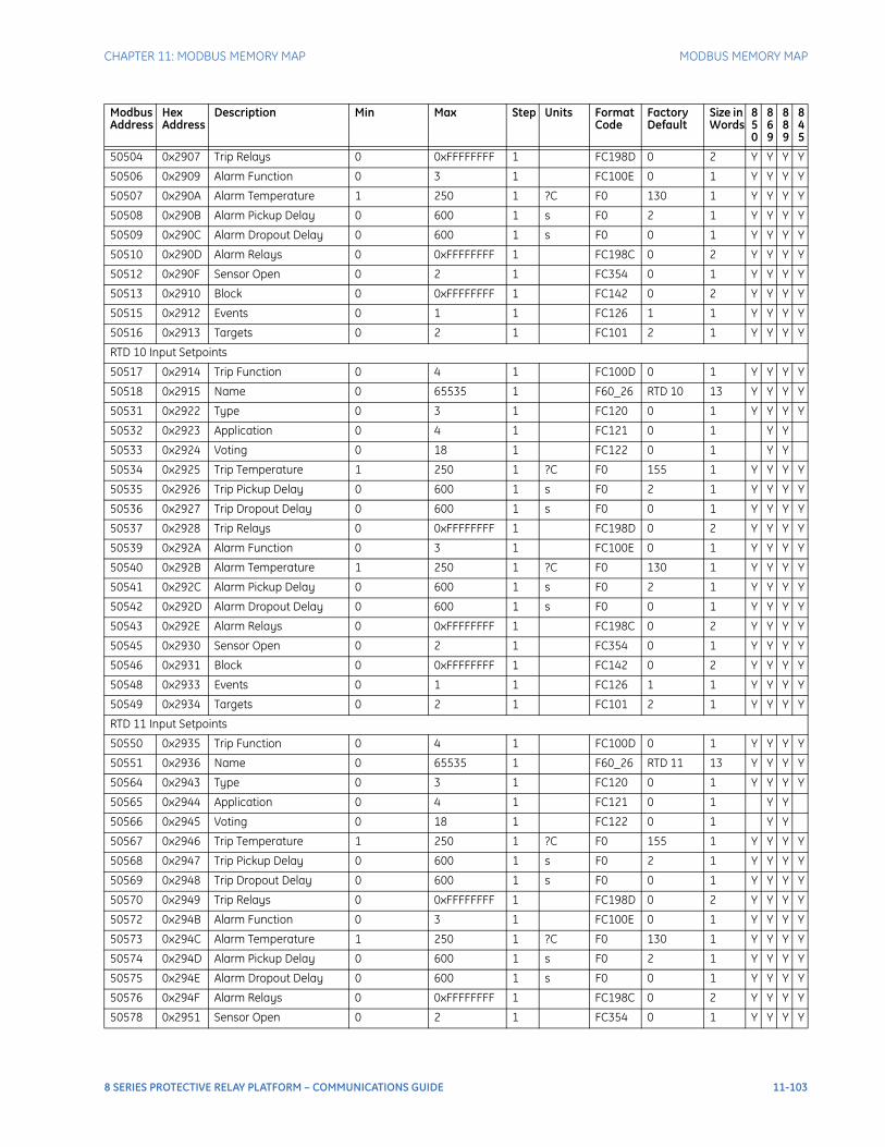
CHAPTER 11: MODBUS MEMORY MAP MODBUS MEMORY MAP
50504 0x2907 Trip Relays 0 0xFFFFFFFF 1 FC198D 0 2 Y Y Y Y
50506 0x2909 Alarm Function 0 3 1 FC100E 0 1 Y Y Y Y
50507 0x290A Alarm Temperature 1 250 1 ?C F0 130 1 Y Y Y Y
50508 0x290B Alarm Pickup Delay 0 600 1 s F0 2 1 Y Y Y Y
50509 0x290C Alarm Dropout Delay 0 600 1 s F0 0 1 Y Y Y Y
50510 0x290D Alarm Relays 0 0xFFFFFFFF 1 FC198C 0 2 Y Y Y Y
50512 0x290F Sensor Open 0 2 1 FC354 0 1 Y Y Y Y
50513 0x2910 Block 0 0xFFFFFFFF 1 FC142 0 2 Y Y Y Y
50515 0x2912 Events 0 1 1 FC126 1 1 Y Y Y Y
50516 0x2913 Targets 0 2 1 FC101 2 1 Y Y Y Y
RTD 10 Input Setpoints
50517 0x2914 Trip Function 0 4 1 FC100D 0 1 Y Y Y Y
50518 0x2915 Name 0 65535 1 F60_26 RTD 10 13 Y Y Y Y
50531 0x2922 Type 0 3 1 FC120 0 1 Y Y Y Y
50532 0x2923 Application 0 4 1 FC121 0 1 Y Y
50533 0x2924 Voting 0 18 1 FC122 0 1 Y Y
50534 0x2925 Trip Temperature 1 250 1 ?C F0 155 1 Y Y Y Y
50535 0x2926 Trip Pickup Delay 0 600 1 s F0 2 1 Y Y Y Y
50536 0x2927 Trip Dropout Delay 0 600 1 s F0 0 1 Y Y Y Y
50537 0x2928 Trip Relays 0 0xFFFFFFFF 1 FC198D 0 2 Y Y Y Y
50539 0x292A Alarm Function 0 3 1 FC100E 0 1 Y Y Y Y
50540 0x292B Alarm Temperature 1 250 1 ?C F0 130 1 Y Y Y Y
50541 0x292C Alarm Pickup Delay 0 600 1 s F0 2 1 Y Y Y Y
50542 0x292D Alarm Dropout Delay 0 600 1 s F0 0 1 Y Y Y Y
50543 0x292E Alarm Relays 0 0xFFFFFFFF 1 FC198C 0 2 Y Y Y Y
50545 0x2930 Sensor Open 0 2 1 FC354 0 1 Y Y Y Y
50546 0x2931 Block 0 0xFFFFFFFF 1 FC142 0 2 Y Y Y Y
50548 0x2933 Events 0 1 1 FC126 1 1 Y Y Y Y
50549 0x2934 Targets 0 2 1 FC101 2 1 Y Y Y Y
RTD 11 Input Setpoints
50550 0x2935 Trip Function 0 4 1 FC100D 0 1 Y Y Y Y
50551 0x2936 Name 0 65535 1 F60_26 RTD 11 13 Y Y Y Y
50564 0x2943 Type 0 3 1 FC120 0 1 Y Y Y Y
50565 0x2944 Application 0 4 1 FC121 0 1 Y Y
50566 0x2945 Voting 0 18 1 FC122 0 1 Y Y
50567 0x2946 Trip Temperature 1 250 1 ?C F0 155 1 Y Y Y Y
50568 0x2947 Trip Pickup Delay 0 600 1 s F0 2 1 Y Y Y Y
50569 0x2948 Trip Dropout Delay 0 600 1 s F0 0 1 Y Y Y Y
50570 0x2949 Trip Relays 0 0xFFFFFFFF 1 FC198D 0 2 Y Y Y Y
50572 0x294B Alarm Function 0 3 1 FC100E 0 1 Y Y Y Y
50573 0x294C Alarm Temperature 1 250 1 ?C F0 130 1 Y Y Y Y
50574 0x294D Alarm Pickup Delay 0 600 1 s F0 2 1 Y Y Y Y
50575 0x294E Alarm Dropout Delay 0 600 1 s F0 0 1 Y Y Y Y
50576 0x294F Alarm Relays 0 0xFFFFFFFF 1 FC198C 0 2 Y Y Y Y
50578 0x2951 Sensor Open 0 2 1 FC354 0 1 Y Y Y Y
Modbus Address
Hex Address
Description Min Max Step Units Format Code
Factory Default
Size in Words
850
869
889
845
8 SERIES PROTECTIVE RELAY PLATFORM – COMMUNICATIONS GUIDE 11-103
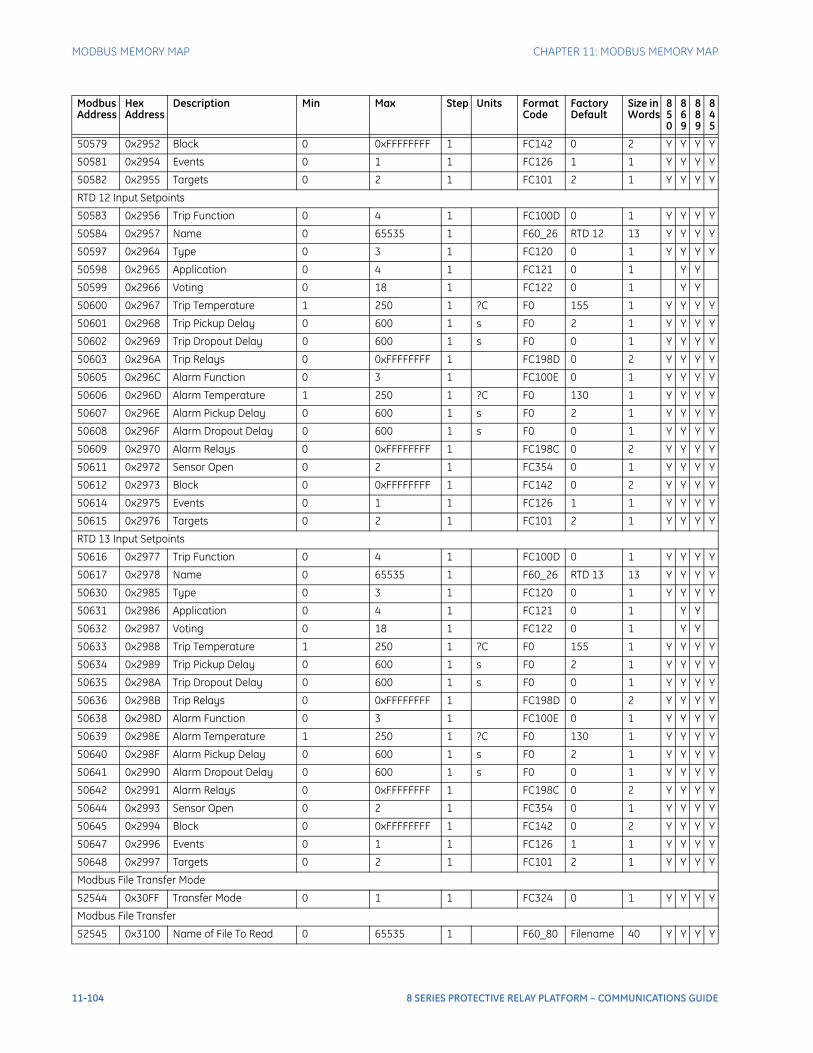
MODBUS MEMORY MAP CHAPTER 11: MODBUS MEMORY MAP
50579 0x2952 Block 0 0xFFFFFFFF 1 FC142 0 2 Y Y Y Y
50581 0x2954 Events 0 1 1 FC126 1 1 Y Y Y Y
50582 0x2955 Targets 0 2 1 FC101 2 1 Y Y Y Y
RTD 12 Input Setpoints
50583 0x2956 Trip Function 0 4 1 FC100D 0 1 Y Y Y Y
50584 0x2957 Name 0 65535 1 F60_26 RTD 12 13 Y Y Y Y
50597 0x2964 Type 0 3 1 FC120 0 1 Y Y Y Y
50598 0x2965 Application 0 4 1 FC121 0 1 Y Y
50599 0x2966 Voting 0 18 1 FC122 0 1 Y Y
50600 0x2967 Trip Temperature 1 250 1 ?C F0 155 1 Y Y Y Y
50601 0x2968 Trip Pickup Delay 0 600 1 s F0 2 1 Y Y Y Y
50602 0x2969 Trip Dropout Delay 0 600 1 s F0 0 1 Y Y Y Y
50603 0x296A Trip Relays 0 0xFFFFFFFF 1 FC198D 0 2 Y Y Y Y
50605 0x296C Alarm Function 0 3 1 FC100E 0 1 Y Y Y Y
50606 0x296D Alarm Temperature 1 250 1 ?C F0 130 1 Y Y Y Y
50607 0x296E Alarm Pickup Delay 0 600 1 s F0 2 1 Y Y Y Y
50608 0x296F Alarm Dropout Delay 0 600 1 s F0 0 1 Y Y Y Y
50609 0x2970 Alarm Relays 0 0xFFFFFFFF 1 FC198C 0 2 Y Y Y Y
50611 0x2972 Sensor Open 0 2 1 FC354 0 1 Y Y Y Y
50612 0x2973 Block 0 0xFFFFFFFF 1 FC142 0 2 Y Y Y Y
50614 0x2975 Events 0 1 1 FC126 1 1 Y Y Y Y
50615 0x2976 Targets 0 2 1 FC101 2 1 Y Y Y Y
RTD 13 Input Setpoints
50616 0x2977 Trip Function 0 4 1 FC100D 0 1 Y Y Y Y
50617 0x2978 Name 0 65535 1 F60_26 RTD 13 13 Y Y Y Y
50630 0x2985 Type 0 3 1 FC120 0 1 Y Y Y Y
50631 0x2986 Application 0 4 1 FC121 0 1 Y Y
50632 0x2987 Voting 0 18 1 FC122 0 1 Y Y
50633 0x2988 Trip Temperature 1 250 1 ?C F0 155 1 Y Y Y Y
50634 0x2989 Trip Pickup Delay 0 600 1 s F0 2 1 Y Y Y Y
50635 0x298A Trip Dropout Delay 0 600 1 s F0 0 1 Y Y Y Y
50636 0x298B Trip Relays 0 0xFFFFFFFF 1 FC198D 0 2 Y Y Y Y
50638 0x298D Alarm Function 0 3 1 FC100E 0 1 Y Y Y Y
50639 0x298E Alarm Temperature 1 250 1 ?C F0 130 1 Y Y Y Y
50640 0x298F Alarm Pickup Delay 0 600 1 s F0 2 1 Y Y Y Y
50641 0x2990 Alarm Dropout Delay 0 600 1 s F0 0 1 Y Y Y Y
50642 0x2991 Alarm Relays 0 0xFFFFFFFF 1 FC198C 0 2 Y Y Y Y
50644 0x2993 Sensor Open 0 2 1 FC354 0 1 Y Y Y Y
50645 0x2994 Block 0 0xFFFFFFFF 1 FC142 0 2 Y Y Y Y
50647 0x2996 Events 0 1 1 FC126 1 1 Y Y Y Y
50648 0x2997 Targets 0 2 1 FC101 2 1 Y Y Y Y
Modbus File Transfer Mode
52544 0x30FF Transfer Mode 0 1 1 FC324 0 1 Y Y Y Y
Modbus File Transfer
52545 0x3100 Name of File To Read 0 65535 1 F60_80 Filename 40 Y Y Y Y
Modbus Address
Hex Address
Description Min Max Step Units Format Code
Factory Default
Size in Words
850
869
889
845
11-104 8 SERIES PROTECTIVE RELAY PLATFORM – COMMUNICATIONS GUIDE
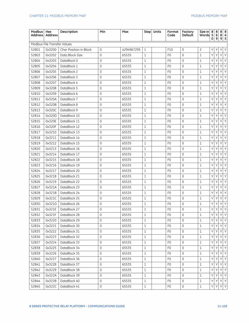
CHAPTER 11: MODBUS MEMORY MAP MODBUS MEMORY MAP
Modbus File Transfer Values
52801 0x3200 Char Position in Block 0 4294967295 1 F10 0 2 Y Y Y Y
52803 0x3202 Data Block Size 0 65535 1 F0 0 1 Y Y Y Y
52804 0x3203 DataBlock 0 0 65535 1 F0 0 1 Y Y Y Y
52805 0x3204 DataBlock 1 0 65535 1 F0 0 1 Y Y Y Y
52806 0x3205 DataBlock 2 0 65535 1 F0 0 1 Y Y Y Y
52807 0x3206 DataBlock 3 0 65535 1 F0 0 1 Y Y Y Y
52808 0x3207 DataBlock 4 0 65535 1 F0 0 1 Y Y Y Y
52809 0x3208 DataBlock 5 0 65535 1 F0 0 1 Y Y Y Y
52810 0x3209 DataBlock 6 0 65535 1 F0 0 1 Y Y Y Y
52811 0x320A DataBlock 7 0 65535 1 F0 0 1 Y Y Y Y
52812 0x320B DataBlock 8 0 65535 1 F0 0 1 Y Y Y Y
52813 0x320C DataBlock 9 0 65535 1 F0 0 1 Y Y Y Y
52814 0x320D DataBlock 10 0 65535 1 F0 0 1 Y Y Y Y
52815 0x320E DataBlock 11 0 65535 1 F0 0 1 Y Y Y Y
52816 0x320F DataBlock 12 0 65535 1 F0 0 1 Y Y Y Y
52817 0x3210 DataBlock 13 0 65535 1 F0 0 1 Y Y Y Y
52818 0x3211 DataBlock 14 0 65535 1 F0 0 1 Y Y Y Y
52819 0x3212 DataBlock 15 0 65535 1 F0 0 1 Y Y Y Y
52820 0x3213 DataBlock 16 0 65535 1 F0 0 1 Y Y Y Y
52821 0x3214 DataBlock 17 0 65535 1 F0 0 1 Y Y Y Y
52822 0x3215 DataBlock 18 0 65535 1 F0 0 1 Y Y Y Y
52823 0x3216 DataBlock 19 0 65535 1 F0 0 1 Y Y Y Y
52824 0x3217 DataBlock 20 0 65535 1 F0 0 1 Y Y Y Y
52825 0x3218 DataBlock 21 0 65535 1 F0 0 1 Y Y Y Y
52826 0x3219 DataBlock 22 0 65535 1 F0 0 1 Y Y Y Y
52827 0x321A DataBlock 23 0 65535 1 F0 0 1 Y Y Y Y
52828 0x321B DataBlock 24 0 65535 1 F0 0 1 Y Y Y Y
52829 0x321C DataBlock 25 0 65535 1 F0 0 1 Y Y Y Y
52830 0x321D DataBlock 26 0 65535 1 F0 0 1 Y Y Y Y
52831 0x321E DataBlock 27 0 65535 1 F0 0 1 Y Y Y Y
52832 0x321F DataBlock 28 0 65535 1 F0 0 1 Y Y Y Y
52833 0x3220 DataBlock 29 0 65535 1 F0 0 1 Y Y Y Y
52834 0x3221 DataBlock 30 0 65535 1 F0 0 1 Y Y Y Y
52835 0x3222 DataBlock 31 0 65535 1 F0 0 1 Y Y Y Y
52836 0x3223 DataBlock 32 0 65535 1 F0 0 1 Y Y Y Y
52837 0x3224 DataBlock 33 0 65535 1 F0 0 1 Y Y Y Y
52838 0x3225 DataBlock 34 0 65535 1 F0 0 1 Y Y Y Y
52839 0x3226 DataBlock 35 0 65535 1 F0 0 1 Y Y Y Y
52840 0x3227 DataBlock 36 0 65535 1 F0 0 1 Y Y Y Y
52841 0x3228 DataBlock 37 0 65535 1 F0 0 1 Y Y Y Y
52842 0x3229 DataBlock 38 0 65535 1 F0 0 1 Y Y Y Y
52843 0x322A DataBlock 39 0 65535 1 F0 0 1 Y Y Y Y
52844 0x322B DataBlock 40 0 65535 1 F0 0 1 Y Y Y Y
52845 0x322C DataBlock 41 0 65535 1 F0 0 1 Y Y Y Y
Modbus Address
Hex Address
Description Min Max Step Units Format Code
Factory Default
Size in Words
850
869
889
845
8 SERIES PROTECTIVE RELAY PLATFORM – COMMUNICATIONS GUIDE 11-105

MODBUS MEMORY MAP CHAPTER 11: MODBUS MEMORY MAP
52846 0x322D DataBlock 42 0 65535 1 F0 0 1 Y Y Y Y
52847 0x322E DataBlock 43 0 65535 1 F0 0 1 Y Y Y Y
52848 0x322F DataBlock 44 0 65535 1 F0 0 1 Y Y Y Y
52849 0x3230 DataBlock 45 0 65535 1 F0 0 1 Y Y Y Y
52850 0x3231 DataBlock 46 0 65535 1 F0 0 1 Y Y Y Y
52851 0x3232 DataBlock 47 0 65535 1 F0 0 1 Y Y Y Y
52852 0x3233 DataBlock 48 0 65535 1 F0 0 1 Y Y Y Y
52853 0x3234 DataBlock 49 0 65535 1 F0 0 1 Y Y Y Y
52854 0x3235 DataBlock 50 0 65535 1 F0 0 1 Y Y Y Y
52855 0x3236 DataBlock 51 0 65535 1 F0 0 1 Y Y Y Y
52856 0x3237 DataBlock 52 0 65535 1 F0 0 1 Y Y Y Y
52857 0x3238 DataBlock 53 0 65535 1 F0 0 1 Y Y Y Y
52858 0x3239 DataBlock 54 0 65535 1 F0 0 1 Y Y Y Y
52859 0x323A DataBlock 55 0 65535 1 F0 0 1 Y Y Y Y
52860 0x323B DataBlock 56 0 65535 1 F0 0 1 Y Y Y Y
52861 0x323C DataBlock 57 0 65535 1 F0 0 1 Y Y Y Y
52862 0x323D DataBlock 58 0 65535 1 F0 0 1 Y Y Y Y
52863 0x323E DataBlock 59 0 65535 1 F0 0 1 Y Y Y Y
52864 0x323F DataBlock 60 0 65535 1 F0 0 1 Y Y Y Y
52865 0x3240 DataBlock 61 0 65535 1 F0 0 1 Y Y Y Y
52866 0x3241 DataBlock 62 0 65535 1 F0 0 1 Y Y Y Y
52867 0x3242 DataBlock 63 0 65535 1 F0 0 1 Y Y Y Y
52868 0x3243 DataBlock 64 0 65535 1 F0 0 1 Y Y Y Y
52869 0x3244 DataBlock 65 0 65535 1 F0 0 1 Y Y Y Y
52870 0x3245 DataBlock 66 0 65535 1 F0 0 1 Y Y Y Y
52871 0x3246 DataBlock 67 0 65535 1 F0 0 1 Y Y Y Y
52872 0x3247 DataBlock 68 0 65535 1 F0 0 1 Y Y Y Y
52873 0x3248 DataBlock 69 0 65535 1 F0 0 1 Y Y Y Y
52874 0x3249 DataBlock 70 0 65535 1 F0 0 1 Y Y Y Y
52875 0x324A DataBlock 71 0 65535 1 F0 0 1 Y Y Y Y
52876 0x324B DataBlock 72 0 65535 1 F0 0 1 Y Y Y Y
52877 0x324C DataBlock 73 0 65535 1 F0 0 1 Y Y Y Y
52878 0x324D DataBlock 74 0 65535 1 F0 0 1 Y Y Y Y
52879 0x324E DataBlock 75 0 65535 1 F0 0 1 Y Y Y Y
52880 0x324F DataBlock 76 0 65535 1 F0 0 1 Y Y Y Y
52881 0x3250 DataBlock 77 0 65535 1 F0 0 1 Y Y Y Y
52882 0x3251 DataBlock 78 0 65535 1 F0 0 1 Y Y Y Y
52883 0x3252 DataBlock 79 0 65535 1 F0 0 1 Y Y Y Y
52884 0x3253 DataBlock 80 0 65535 1 F0 0 1 Y Y Y Y
52885 0x3254 DataBlock 81 0 65535 1 F0 0 1 Y Y Y Y
52886 0x3255 DataBlock 82 0 65535 1 F0 0 1 Y Y Y Y
52887 0x3256 DataBlock 83 0 65535 1 F0 0 1 Y Y Y Y
52888 0x3257 DataBlock 84 0 65535 1 F0 0 1 Y Y Y Y
52889 0x3258 DataBlock 85 0 65535 1 F0 0 1 Y Y Y Y
52890 0x3259 DataBlock 86 0 65535 1 F0 0 1 Y Y Y Y
Modbus Address
Hex Address
Description Min Max Step Units Format Code
Factory Default
Size in Words
850
869
889
845
11-106 8 SERIES PROTECTIVE RELAY PLATFORM – COMMUNICATIONS GUIDE
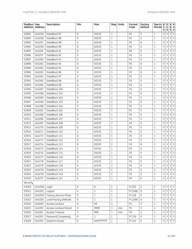
CHAPTER 11: MODBUS MEMORY MAP MODBUS MEMORY MAP
52891 0x325A DataBlock 87 0 65535 1 F0 0 1 Y Y Y Y
52892 0x325B DataBlock 88 0 65535 1 F0 0 1 Y Y Y Y
52893 0x325C DataBlock 89 0 65535 1 F0 0 1 Y Y Y Y
52894 0x325D DataBlock 90 0 65535 1 F0 0 1 Y Y Y Y
52895 0x325E DataBlock 91 0 65535 1 F0 0 1 Y Y Y Y
52896 0x325F DataBlock 92 0 65535 1 F0 0 1 Y Y Y Y
52897 0x3260 DataBlock 93 0 65535 1 F0 0 1 Y Y Y Y
52898 0x3261 DataBlock 94 0 65535 1 F0 0 1 Y Y Y Y
52899 0x3262 DataBlock 95 0 65535 1 F0 0 1 Y Y Y Y
52900 0x3263 DataBlock 96 0 65535 1 F0 0 1 Y Y Y Y
52901 0x3264 DataBlock 97 0 65535 1 F0 0 1 Y Y Y Y
52902 0x3265 DataBlock 98 0 65535 1 F0 0 1 Y Y Y Y
52903 0x3266 DataBlock 99 0 65535 1 F0 0 1 Y Y Y Y
52904 0x3267 DataBlock 100 0 65535 1 F0 0 1 Y Y Y Y
52905 0x3268 DataBlock 101 0 65535 1 F0 0 1 Y Y Y Y
52906 0x3269 DataBlock 102 0 65535 1 F0 0 1 Y Y Y Y
52907 0x326A DataBlock 103 0 65535 1 F0 0 1 Y Y Y Y
52908 0x326B DataBlock 104 0 65535 1 F0 0 1 Y Y Y Y
52909 0x326C DataBlock 105 0 65535 1 F0 0 1 Y Y Y Y
52910 0x326D DataBlock 106 0 65535 1 F0 0 1 Y Y Y Y
52911 0x326E DataBlock 107 0 65535 1 F0 0 1 Y Y Y Y
52912 0x326F DataBlock 108 0 65535 1 F0 0 1 Y Y Y Y
52913 0x3270 DataBlock 109 0 65535 1 F0 0 1 Y Y Y Y
52914 0x3271 DataBlock 110 0 65535 1 F0 0 1 Y Y Y Y
52915 0x3272 DataBlock 111 0 65535 1 F0 0 1 Y Y Y Y
52916 0x3273 DataBlock 112 0 65535 1 F0 0 1 Y Y Y Y
52917 0x3274 DataBlock 113 0 65535 1 F0 0 1 Y Y Y Y
52918 0x3275 DataBlock 114 0 65535 1 F0 0 1 Y Y Y Y
52919 0x3276 DataBlock 115 0 65535 1 F0 0 1 Y Y Y Y
52920 0x3277 DataBlock 116 0 65535 1 F0 0 1 Y Y Y Y
52921 0x3278 DataBlock 117 0 65535 1 F0 0 1 Y Y Y Y
52922 0x3279 DataBlock 118 0 65535 1 F0 0 1 Y Y Y Y
52923 0x327A DataBlock 119 0 65535 1 F0 0 1 Y Y Y Y
52924 0x327B DataBlock 120 0 65535 1 F0 0 1 Y Y Y Y
52925 0x327C DataBlock 121 0 65535 1 F0 0 1 Y Y Y Y
Security
53020 0x32DB Login 0 8 1 FC252 0 1 Y Y Y Y
53021 0x32DC Logout 0 1 1 FC126B 0 1 Y Y Y Y
53022 0x32DD Factory Service Mode 0 1 1 FC126 0 1 Y Y Y Y
53023 0x32DE Load Factory Defaults 0 1 1 FC126B 0 1 Y Y Y Y
53024 0x32DF Access Lockout 0 99 1 F0 3 1 Y Y Y Y
53025 0x32E0 Access Lockout Period 0 9999 1 min F0 3 1 Y Y Y Y
53026 0x32E1 Access Timeout 2 999 1 min F0 5 1 Y Y Y Y
53027 0x32E2 Password Complexity 0 1 1 FC126 0 1 Y Y Y Y
53028 0x32E3 Setpoint Access 0 0xFFFFFFFF 1 FC142 0 2 Y Y Y Y
Modbus Address
Hex Address
Description Min Max Step Units Format Code
Factory Default
Size in Words
850
869
889
845
8 SERIES PROTECTIVE RELAY PLATFORM – COMMUNICATIONS GUIDE 11-107
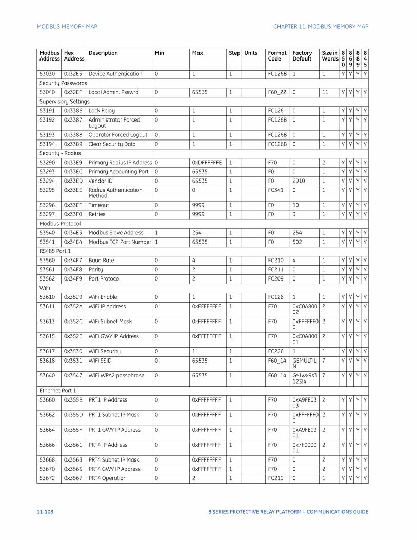
MODBUS MEMORY MAP CHAPTER 11: MODBUS MEMORY MAP
53030 0x32E5 Device Authentication 0 1 1 FC126B 1 1 Y Y Y Y
Security Passwords
53040 0x32EF Local Admin. Psswrd 0 65535 1 F60_22 0 11 Y Y Y Y
Supervisory Settings
53191 0x3386 Lock Relay 0 1 1 FC126 0 1 Y Y Y Y
53192 0x3387 Administrator Forced Logout
0 1 1 FC126B 0 1 Y Y Y Y
53193 0x3388 Operator Forced Logout 0 1 1 FC126B 0 1 Y Y Y Y
53194 0x3389 Clear Security Data 0 1 1 FC126B 0 1 Y Y Y Y
Security - Radius
53290 0x33E9 Primary Radius IP Address 0 0xDFFFFFFE 1 F70 0 2 Y Y Y Y
53293 0x33EC Primary Accounting Port 0 65535 1 F0 0 1 Y Y Y Y
53294 0x33ED Vendor ID 0 65535 1 F0 2910 1 Y Y Y Y
53295 0x33EE Radius Authentication Method
0 0 1 FC341 0 1 Y Y Y Y
53296 0x33EF Timeout 0 9999 1 F0 10 1 Y Y Y Y
53297 0x33F0 Retries 0 9999 1 F0 3 1 Y Y Y Y
Modbus Protocol
53540 0x34E3 Modbus Slave Address 1 254 1 F0 254 1 Y Y Y Y
53541 0x34E4 Modbus TCP Port Number 1 65535 1 F0 502 1 Y Y Y Y
RS485 Port 1
53560 0x34F7 Baud Rate 0 4 1 FC210 4 1 Y Y Y Y
53561 0x34F8 Parity 0 2 1 FC211 0 1 Y Y Y Y
53562 0x34F9 Port Protocol 0 2 1 FC209 0 1 Y Y Y Y
WiFi
53610 0x3529 WiFi Enable 0 1 1 FC126 1 1 Y Y Y Y
53611 0x352A WiFi IP Address 0 0xFFFFFFFF 1 F70 0xC0A80002
2 Y Y Y Y
53613 0x352C WiFi Subnet Mask 0 0xFFFFFFFF 1 F70 0xFFFFFF00
2 Y Y Y Y
53615 0x352E WiFi GWY IP Address 0 0xFFFFFFFF 1 F70 0xC0A80001
2 Y Y Y Y
53617 0x3530 WiFi Security 0 1 1 FC226 1 1 Y Y Y Y
53618 0x3531 WiFi SSID 0 65535 1 F60_14 GEMULTILIN
7 Y Y Y Y
53640 0x3547 WiFi WPA2 passphrase 0 65535 1 F60_14 Ge1wx9s3123!4
7 Y Y Y Y
Ethernet Port 1
53660 0x355B PRT1 IP Address 0 0xFFFFFFFF 1 F70 0xA9FE0303
2 Y Y Y Y
53662 0x355D PRT1 Subnet IP Mask 0 0xFFFFFFFF 1 F70 0xFFFFFF00
2 Y Y Y Y
53664 0x355F PRT1 GWY IP Address 0 0xFFFFFFFF 1 F70 0xA9FE0301
2 Y Y Y Y
53666 0x3561 PRT4 IP Address 0 0xFFFFFFFF 1 F70 0x7F000001
2 Y Y Y Y
53668 0x3563 PRT4 Subnet IP Mask 0 0xFFFFFFFF 1 F70 0 2 Y Y Y Y
53670 0x3565 PRT4 GWY IP Address 0 0xFFFFFFFF 1 F70 0 2 Y Y Y Y
53672 0x3567 PRT4 Operation 0 2 1 FC219 0 1 Y Y Y Y
Modbus Address
Hex Address
Description Min Max Step Units Format Code
Factory Default
Size in Words
850
869
889
845
11-108 8 SERIES PROTECTIVE RELAY PLATFORM – COMMUNICATIONS GUIDE
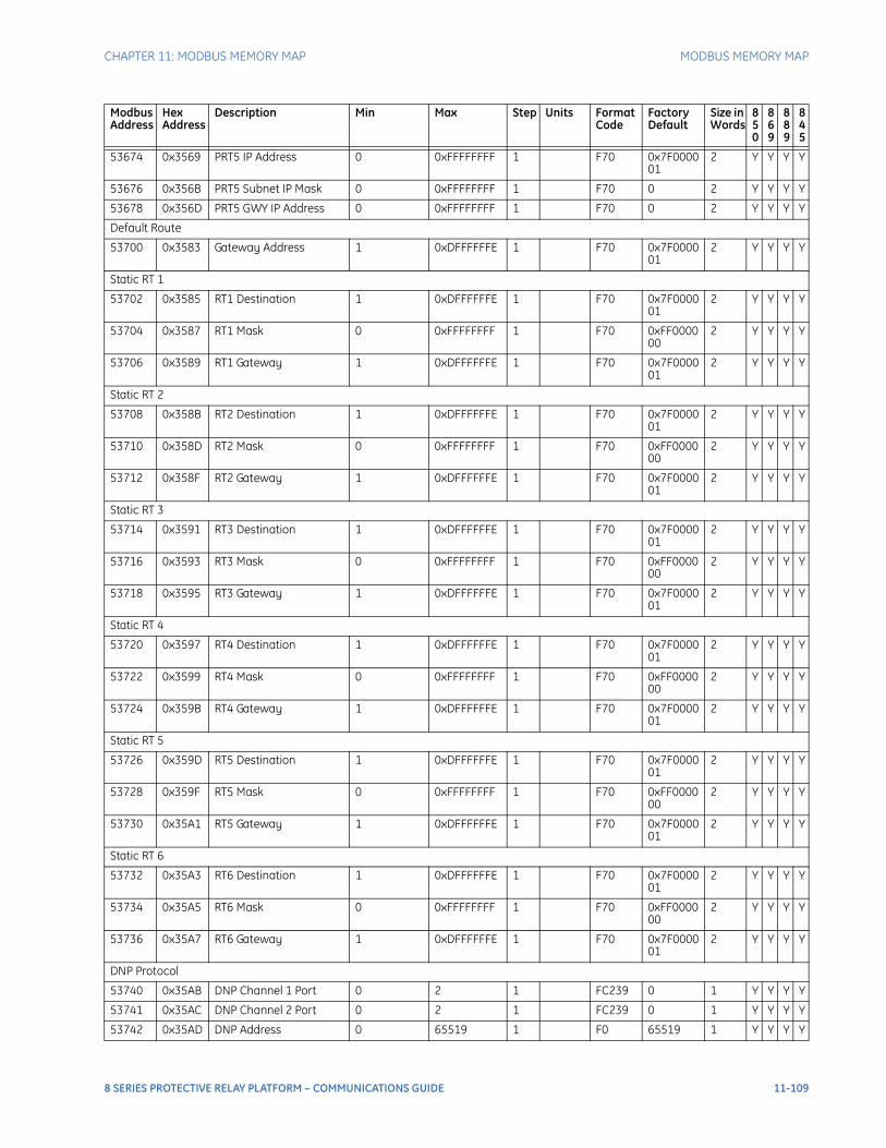
CHAPTER 11: MODBUS MEMORY MAP MODBUS MEMORY MAP
53674 0x3569 PRT5 IP Address 0 0xFFFFFFFF 1 F70 0x7F000001
2 Y Y Y Y
53676 0x356B PRT5 Subnet IP Mask 0 0xFFFFFFFF 1 F70 0 2 Y Y Y Y
53678 0x356D PRT5 GWY IP Address 0 0xFFFFFFFF 1 F70 0 2 Y Y Y Y
Default Route
53700 0x3583 Gateway Address 1 0xDFFFFFFE 1 F70 0x7F000001
2 Y Y Y Y
Static RT 1
53702 0x3585 RT1 Destination 1 0xDFFFFFFE 1 F70 0x7F000001
2 Y Y Y Y
53704 0x3587 RT1 Mask 0 0xFFFFFFFF 1 F70 0xFF000000
2 Y Y Y Y
53706 0x3589 RT1 Gateway 1 0xDFFFFFFE 1 F70 0x7F000001
2 Y Y Y Y
Static RT 2
53708 0x358B RT2 Destination 1 0xDFFFFFFE 1 F70 0x7F000001
2 Y Y Y Y
53710 0x358D RT2 Mask 0 0xFFFFFFFF 1 F70 0xFF000000
2 Y Y Y Y
53712 0x358F RT2 Gateway 1 0xDFFFFFFE 1 F70 0x7F000001
2 Y Y Y Y
Static RT 3
53714 0x3591 RT3 Destination 1 0xDFFFFFFE 1 F70 0x7F000001
2 Y Y Y Y
53716 0x3593 RT3 Mask 0 0xFFFFFFFF 1 F70 0xFF000000
2 Y Y Y Y
53718 0x3595 RT3 Gateway 1 0xDFFFFFFE 1 F70 0x7F000001
2 Y Y Y Y
Static RT 4
53720 0x3597 RT4 Destination 1 0xDFFFFFFE 1 F70 0x7F000001
2 Y Y Y Y
53722 0x3599 RT4 Mask 0 0xFFFFFFFF 1 F70 0xFF000000
2 Y Y Y Y
53724 0x359B RT4 Gateway 1 0xDFFFFFFE 1 F70 0x7F000001
2 Y Y Y Y
Static RT 5
53726 0x359D RT5 Destination 1 0xDFFFFFFE 1 F70 0x7F000001
2 Y Y Y Y
53728 0x359F RT5 Mask 0 0xFFFFFFFF 1 F70 0xFF000000
2 Y Y Y Y
53730 0x35A1 RT5 Gateway 1 0xDFFFFFFE 1 F70 0x7F000001
2 Y Y Y Y
Static RT 6
53732 0x35A3 RT6 Destination 1 0xDFFFFFFE 1 F70 0x7F000001
2 Y Y Y Y
53734 0x35A5 RT6 Mask 0 0xFFFFFFFF 1 F70 0xFF000000
2 Y Y Y Y
53736 0x35A7 RT6 Gateway 1 0xDFFFFFFE 1 F70 0x7F000001
2 Y Y Y Y
DNP Protocol
53740 0x35AB DNP Channel 1 Port 0 2 1 FC239 0 1 Y Y Y Y
53741 0x35AC DNP Channel 2 Port 0 2 1 FC239 0 1 Y Y Y Y
53742 0x35AD DNP Address 0 65519 1 F0 65519 1 Y Y Y Y
Modbus Address
Hex Address
Description Min Max Step Units Format Code
Factory Default
Size in Words
850
869
889
845
8 SERIES PROTECTIVE RELAY PLATFORM – COMMUNICATIONS GUIDE 11-109
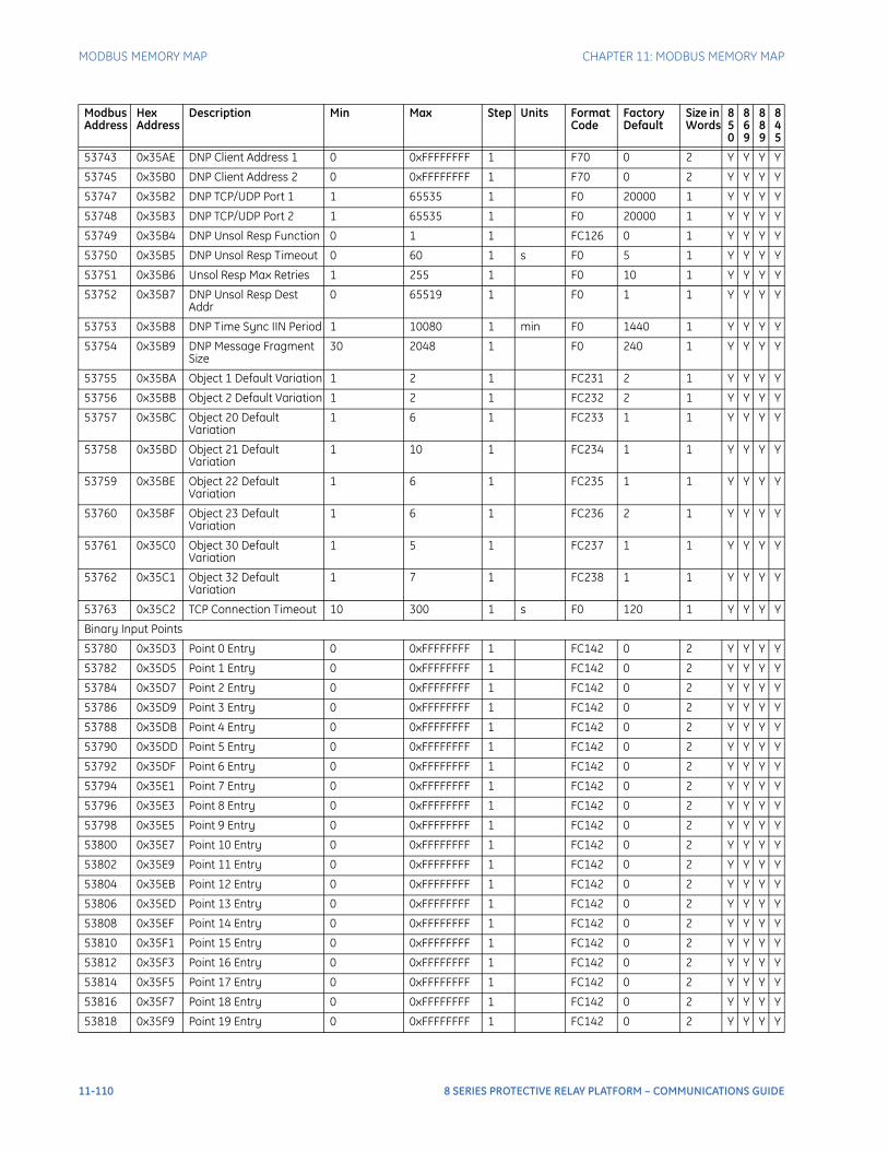
MODBUS MEMORY MAP CHAPTER 11: MODBUS MEMORY MAP
53743 0x35AE DNP Client Address 1 0 0xFFFFFFFF 1 F70 0 2 Y Y Y Y
53745 0x35B0 DNP Client Address 2 0 0xFFFFFFFF 1 F70 0 2 Y Y Y Y
53747 0x35B2 DNP TCP/UDP Port 1 1 65535 1 F0 20000 1 Y Y Y Y
53748 0x35B3 DNP TCP/UDP Port 2 1 65535 1 F0 20000 1 Y Y Y Y
53749 0x35B4 DNP Unsol Resp Function 0 1 1 FC126 0 1 Y Y Y Y
53750 0x35B5 DNP Unsol Resp Timeout 0 60 1 s F0 5 1 Y Y Y Y
53751 0x35B6 Unsol Resp Max Retries 1 255 1 F0 10 1 Y Y Y Y
53752 0x35B7 DNP Unsol Resp Dest Addr
0 65519 1 F0 1 1 Y Y Y Y
53753 0x35B8 DNP Time Sync IIN Period 1 10080 1 min F0 1440 1 Y Y Y Y
53754 0x35B9 DNP Message Fragment Size
30 2048 1 F0 240 1 Y Y Y Y
53755 0x35BA Object 1 Default Variation 1 2 1 FC231 2 1 Y Y Y Y
53756 0x35BB Object 2 Default Variation 1 2 1 FC232 2 1 Y Y Y Y
53757 0x35BC Object 20 Default Variation
1 6 1 FC233 1 1 Y Y Y Y
53758 0x35BD Object 21 Default Variation
1 10 1 FC234 1 1 Y Y Y Y
53759 0x35BE Object 22 Default Variation
1 6 1 FC235 1 1 Y Y Y Y
53760 0x35BF Object 23 Default Variation
1 6 1 FC236 2 1 Y Y Y Y
53761 0x35C0 Object 30 Default Variation
1 5 1 FC237 1 1 Y Y Y Y
53762 0x35C1 Object 32 Default Variation
1 7 1 FC238 1 1 Y Y Y Y
53763 0x35C2 TCP Connection Timeout 10 300 1 s F0 120 1 Y Y Y Y
Binary Input Points
53780 0x35D3 Point 0 Entry 0 0xFFFFFFFF 1 FC142 0 2 Y Y Y Y
53782 0x35D5 Point 1 Entry 0 0xFFFFFFFF 1 FC142 0 2 Y Y Y Y
53784 0x35D7 Point 2 Entry 0 0xFFFFFFFF 1 FC142 0 2 Y Y Y Y
53786 0x35D9 Point 3 Entry 0 0xFFFFFFFF 1 FC142 0 2 Y Y Y Y
53788 0x35DB Point 4 Entry 0 0xFFFFFFFF 1 FC142 0 2 Y Y Y Y
53790 0x35DD Point 5 Entry 0 0xFFFFFFFF 1 FC142 0 2 Y Y Y Y
53792 0x35DF Point 6 Entry 0 0xFFFFFFFF 1 FC142 0 2 Y Y Y Y
53794 0x35E1 Point 7 Entry 0 0xFFFFFFFF 1 FC142 0 2 Y Y Y Y
53796 0x35E3 Point 8 Entry 0 0xFFFFFFFF 1 FC142 0 2 Y Y Y Y
53798 0x35E5 Point 9 Entry 0 0xFFFFFFFF 1 FC142 0 2 Y Y Y Y
53800 0x35E7 Point 10 Entry 0 0xFFFFFFFF 1 FC142 0 2 Y Y Y Y
53802 0x35E9 Point 11 Entry 0 0xFFFFFFFF 1 FC142 0 2 Y Y Y Y
53804 0x35EB Point 12 Entry 0 0xFFFFFFFF 1 FC142 0 2 Y Y Y Y
53806 0x35ED Point 13 Entry 0 0xFFFFFFFF 1 FC142 0 2 Y Y Y Y
53808 0x35EF Point 14 Entry 0 0xFFFFFFFF 1 FC142 0 2 Y Y Y Y
53810 0x35F1 Point 15 Entry 0 0xFFFFFFFF 1 FC142 0 2 Y Y Y Y
53812 0x35F3 Point 16 Entry 0 0xFFFFFFFF 1 FC142 0 2 Y Y Y Y
53814 0x35F5 Point 17 Entry 0 0xFFFFFFFF 1 FC142 0 2 Y Y Y Y
53816 0x35F7 Point 18 Entry 0 0xFFFFFFFF 1 FC142 0 2 Y Y Y Y
53818 0x35F9 Point 19 Entry 0 0xFFFFFFFF 1 FC142 0 2 Y Y Y Y
Modbus Address
Hex Address
Description Min Max Step Units Format Code
Factory Default
Size in Words
850
869
889
845
11-110 8 SERIES PROTECTIVE RELAY PLATFORM – COMMUNICATIONS GUIDE

CHAPTER 11: MODBUS MEMORY MAP MODBUS MEMORY MAP
53820 0x35FB Point 20 Entry 0 0xFFFFFFFF 1 FC142 0 2 Y Y Y Y
53822 0x35FD Point 21 Entry 0 0xFFFFFFFF 1 FC142 0 2 Y Y Y Y
53824 0x35FF Point 22 Entry 0 0xFFFFFFFF 1 FC142 0 2 Y Y Y Y
53826 0x3601 Point 23 Entry 0 0xFFFFFFFF 1 FC142 0 2 Y Y Y Y
53828 0x3603 Point 24 Entry 0 0xFFFFFFFF 1 FC142 0 2 Y Y Y Y
53830 0x3605 Point 25 Entry 0 0xFFFFFFFF 1 FC142 0 2 Y Y Y Y
53832 0x3607 Point 26 Entry 0 0xFFFFFFFF 1 FC142 0 2 Y Y Y Y
53834 0x3609 Point 27 Entry 0 0xFFFFFFFF 1 FC142 0 2 Y Y Y Y
53836 0x360B Point 28 Entry 0 0xFFFFFFFF 1 FC142 0 2 Y Y Y Y
53838 0x360D Point 29 Entry 0 0xFFFFFFFF 1 FC142 0 2 Y Y Y Y
53840 0x360F Point 30 Entry 0 0xFFFFFFFF 1 FC142 0 2 Y Y Y Y
53842 0x3611 Point 31 Entry 0 0xFFFFFFFF 1 FC142 0 2 Y Y Y Y
53844 0x3613 Point 32 Entry 0 0xFFFFFFFF 1 FC142 0 2 Y Y Y Y
53846 0x3615 Point 33 Entry 0 0xFFFFFFFF 1 FC142 0 2 Y Y Y Y
53848 0x3617 Point 34 Entry 0 0xFFFFFFFF 1 FC142 0 2 Y Y Y Y
53850 0x3619 Point 35 Entry 0 0xFFFFFFFF 1 FC142 0 2 Y Y Y Y
53852 0x361B Point 36 Entry 0 0xFFFFFFFF 1 FC142 0 2 Y Y Y Y
53854 0x361D Point 37 Entry 0 0xFFFFFFFF 1 FC142 0 2 Y Y Y Y
53856 0x361F Point 38 Entry 0 0xFFFFFFFF 1 FC142 0 2 Y Y Y Y
53858 0x3621 Point 39 Entry 0 0xFFFFFFFF 1 FC142 0 2 Y Y Y Y
53860 0x3623 Point 40 Entry 0 0xFFFFFFFF 1 FC142 0 2 Y Y Y Y
53862 0x3625 Point 41 Entry 0 0xFFFFFFFF 1 FC142 0 2 Y Y Y Y
53864 0x3627 Point 42 Entry 0 0xFFFFFFFF 1 FC142 0 2 Y Y Y Y
53866 0x3629 Point 43 Entry 0 0xFFFFFFFF 1 FC142 0 2 Y Y Y Y
53868 0x362B Point 44 Entry 0 0xFFFFFFFF 1 FC142 0 2 Y Y Y Y
53870 0x362D Point 45 Entry 0 0xFFFFFFFF 1 FC142 0 2 Y Y Y Y
53872 0x362F Point 46 Entry 0 0xFFFFFFFF 1 FC142 0 2 Y Y Y Y
53874 0x3631 Point 47 Entry 0 0xFFFFFFFF 1 FC142 0 2 Y Y Y Y
53876 0x3633 Point 48 Entry 0 0xFFFFFFFF 1 FC142 0 2 Y Y Y Y
53878 0x3635 Point 49 Entry 0 0xFFFFFFFF 1 FC142 0 2 Y Y Y Y
53880 0x3637 Point 50 Entry 0 0xFFFFFFFF 1 FC142 0 2 Y Y Y Y
53882 0x3639 Point 51 Entry 0 0xFFFFFFFF 1 FC142 0 2 Y Y Y Y
53884 0x363B Point 52 Entry 0 0xFFFFFFFF 1 FC142 0 2 Y Y Y Y
53886 0x363D Point 53 Entry 0 0xFFFFFFFF 1 FC142 0 2 Y Y Y Y
53888 0x363F Point 54 Entry 0 0xFFFFFFFF 1 FC142 0 2 Y Y Y Y
53890 0x3641 Point 55 Entry 0 0xFFFFFFFF 1 FC142 0 2 Y Y Y Y
53892 0x3643 Point 56 Entry 0 0xFFFFFFFF 1 FC142 0 2 Y Y Y Y
53894 0x3645 Point 57 Entry 0 0xFFFFFFFF 1 FC142 0 2 Y Y Y Y
53896 0x3647 Point 58 Entry 0 0xFFFFFFFF 1 FC142 0 2 Y Y Y Y
53898 0x3649 Point 59 Entry 0 0xFFFFFFFF 1 FC142 0 2 Y Y Y Y
53900 0x364B Point 60 Entry 0 0xFFFFFFFF 1 FC142 0 2 Y Y Y Y
53902 0x364D Point 61 Entry 0 0xFFFFFFFF 1 FC142 0 2 Y Y Y Y
53904 0x364F Point 62 Entry 0 0xFFFFFFFF 1 FC142 0 2 Y Y Y Y
53906 0x3651 Point 63 Entry 0 0xFFFFFFFF 1 FC142 0 2 Y Y Y Y
53908 0x3653 Point 64 Entry 0 0xFFFFFFFF 1 FC142 0 2 Y Y Y Y
Modbus Address
Hex Address
Description Min Max Step Units Format Code
Factory Default
Size in Words
850
869
889
845
8 SERIES PROTECTIVE RELAY PLATFORM – COMMUNICATIONS GUIDE 11-111
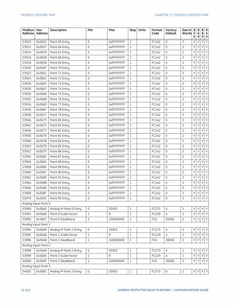
MODBUS MEMORY MAP CHAPTER 11: MODBUS MEMORY MAP
53910 0x3655 Point 65 Entry 0 0xFFFFFFFF 1 FC142 0 2 Y Y Y Y
53912 0x3657 Point 66 Entry 0 0xFFFFFFFF 1 FC142 0 2 Y Y Y Y
53914 0x3659 Point 67 Entry 0 0xFFFFFFFF 1 FC142 0 2 Y Y Y Y
53916 0x365B Point 68 Entry 0 0xFFFFFFFF 1 FC142 0 2 Y Y Y Y
53918 0x365D Point 69 Entry 0 0xFFFFFFFF 1 FC142 0 2 Y Y Y Y
53920 0x365F Point 70 Entry 0 0xFFFFFFFF 1 FC142 0 2 Y Y Y Y
53922 0x3661 Point 71 Entry 0 0xFFFFFFFF 1 FC142 0 2 Y Y Y Y
53924 0x3663 Point 72 Entry 0 0xFFFFFFFF 1 FC142 0 2 Y Y Y Y
53926 0x3665 Point 73 Entry 0 0xFFFFFFFF 1 FC142 0 2 Y Y Y Y
53928 0x3667 Point 74 Entry 0 0xFFFFFFFF 1 FC142 0 2 Y Y Y Y
53930 0x3669 Point 75 Entry 0 0xFFFFFFFF 1 FC142 0 2 Y Y Y Y
53932 0x366B Point 76 Entry 0 0xFFFFFFFF 1 FC142 0 2 Y Y Y Y
53934 0x366D Point 77 Entry 0 0xFFFFFFFF 1 FC142 0 2 Y Y Y Y
53936 0x366F Point 78 Entry 0 0xFFFFFFFF 1 FC142 0 2 Y Y Y Y
53938 0x3671 Point 79 Entry 0 0xFFFFFFFF 1 FC142 0 2 Y Y Y Y
53940 0x3673 Point 80 Entry 0 0xFFFFFFFF 1 FC142 0 2 Y Y Y Y
53942 0x3675 Point 81 Entry 0 0xFFFFFFFF 1 FC142 0 2 Y Y Y Y
53944 0x3677 Point 82 Entry 0 0xFFFFFFFF 1 FC142 0 2 Y Y Y Y
53946 0x3679 Point 83 Entry 0 0xFFFFFFFF 1 FC142 0 2 Y Y Y Y
53948 0x367B Point 84 Entry 0 0xFFFFFFFF 1 FC142 0 2 Y Y Y Y
53950 0x367D Point 85 Entry 0 0xFFFFFFFF 1 FC142 0 2 Y Y Y Y
53952 0x367F Point 86 Entry 0 0xFFFFFFFF 1 FC142 0 2 Y Y Y Y
53954 0x3681 Point 87 Entry 0 0xFFFFFFFF 1 FC142 0 2 Y Y Y Y
53956 0x3683 Point 88 Entry 0 0xFFFFFFFF 1 FC142 0 2 Y Y Y Y
53958 0x3685 Point 89 Entry 0 0xFFFFFFFF 1 FC142 0 2 Y Y Y Y
53960 0x3687 Point 90 Entry 0 0xFFFFFFFF 1 FC142 0 2 Y Y Y Y
53962 0x3689 Point 91 Entry 0 0xFFFFFFFF 1 FC142 0 2 Y Y Y Y
53964 0x368B Point 92 Entry 0 0xFFFFFFFF 1 FC142 0 2 Y Y Y Y
53966 0x368D Point 93 Entry 0 0xFFFFFFFF 1 FC142 0 2 Y Y Y Y
53968 0x368F Point 94 Entry 0 0xFFFFFFFF 1 FC142 0 2 Y Y Y Y
53970 0x3691 Point 95 Entry 0 0xFFFFFFFF 1 FC142 0 2 Y Y Y Y
Analog Input Point 0
53990 0x36A5 Analog IP Point 0 Entry 0 35903 1 FC273 0 1 Y Y Y Y
53991 0x36A6 Point 0 Scale Factor 1 9 1 FC229 4 1 Y Y Y Y
53992 0x36A7 Point 0 Deadband 1 100000000 1 F10 30000 2 Y Y Y Y
Analog Input Point 1
53994 0x36A9 Analog IP Point 1 Entry 0 35903 1 FC273 0 1 Y Y Y Y
53995 0x36AA Point 1 Scale Factor 1 9 1 FC229 4 1 Y Y Y Y
53996 0x36AB Point 1 Deadband 1 100000000 1 F10 30000 2 Y Y Y Y
Analog Input Point 2
53998 0x36AD Analog IP Point 2 Entry 0 35903 1 FC273 0 1 Y Y Y Y
53999 0x36AE Point 2 Scale Factor 1 9 1 FC229 4 1 Y Y Y Y
54000 0x36AF Point 2 Deadband 1 100000000 1 F10 30000 2 Y Y Y Y
Analog Input Point 3
54002 0x36B1 Analog IP Point 3 Entry 0 35903 1 FC273 0 1 Y Y Y Y
Modbus Address
Hex Address
Description Min Max Step Units Format Code
Factory Default
Size in Words
850
869
889
845
11-112 8 SERIES PROTECTIVE RELAY PLATFORM – COMMUNICATIONS GUIDE

CHAPTER 11: MODBUS MEMORY MAP MODBUS MEMORY MAP
54003 0x36B2 Point 3 Scale Factor 1 9 1 FC229 4 1 Y Y Y Y
54004 0x36B3 Point 3 Deadband 1 100000000 1 F10 30000 2 Y Y Y Y
Analog Input Point 4
54006 0x36B5 Analog IP Point 4 Entry 0 35903 1 FC273 0 1 Y Y Y Y
54007 0x36B6 Point 4 Scale Factor 1 9 1 FC229 4 1 Y Y Y Y
54008 0x36B7 Point 4 Deadband 1 100000000 1 F10 30000 2 Y Y Y Y
Analog Input Point 5
54010 0x36B9 Analog IP Point 5 Entry 0 35903 1 FC273 0 1 Y Y Y Y
54011 0x36BA Point 5 Scale Factor 1 9 1 FC229 4 1 Y Y Y Y
54012 0x36BB Point 5 Deadband 1 100000000 1 F10 30000 2 Y Y Y Y
Analog Input Point 6
54014 0x36BD Analog IP Point 6 Entry 0 35903 1 FC273 0 1 Y Y Y Y
54015 0x36BE Point 6 Scale Factor 1 9 1 FC229 4 1 Y Y Y Y
54016 0x36BF Point 6 Deadband 1 100000000 1 F10 30000 2 Y Y Y Y
Analog Input Point 7
54018 0x36C1 Analog IP Point 7 Entry 0 35903 1 FC273 0 1 Y Y Y Y
54019 0x36C2 Point 7 Scale Factor 1 9 1 FC229 4 1 Y Y Y Y
54020 0x36C3 Point 7 Deadband 1 100000000 1 F10 30000 2 Y Y Y Y
Analog Input Point 8
54022 0x36C5 Analog IP Point 8 Entry 0 35903 1 FC273 0 1 Y Y Y Y
54023 0x36C6 Point 8 Scale Factor 1 9 1 FC229 4 1 Y Y Y Y
54024 0x36C7 Point 8 Deadband 1 100000000 1 F10 30000 2 Y Y Y Y
Analog Input Point 9
54026 0x36C9 Analog IP Point 9 Entry 0 35903 1 FC273 0 1 Y Y Y Y
54027 0x36CA Point 9 Scale Factor 1 9 1 FC229 4 1 Y Y Y Y
54028 0x36CB Point 9 Deadband 1 100000000 1 F10 30000 2 Y Y Y Y
Analog Input Point 10
54030 0x36CD Analog IP Point 10 Entry 0 35903 1 FC273 0 1 Y Y Y Y
54031 0x36CE Point 10 Scale Factor 1 9 1 FC229 4 1 Y Y Y Y
54032 0x36CF Point 10 Deadband 1 100000000 1 F10 30000 2 Y Y Y Y
Analog Input Point 11
54034 0x36D1 Analog IP Point 11 Entry 0 35903 1 FC273 0 1 Y Y Y Y
54035 0x36D2 Point 11 Scale Factor 1 9 1 FC229 4 1 Y Y Y Y
54036 0x36D3 Point 11 Deadband 1 100000000 1 F10 30000 2 Y Y Y Y
Analog Input Point 12
54038 0x36D5 Analog IP Point 12 Entry 0 35903 1 FC273 0 1 Y Y Y Y
54039 0x36D6 Point 12 Scale Factor 1 9 1 FC229 4 1 Y Y Y Y
54040 0x36D7 Point 12 Deadband 1 100000000 1 F10 30000 2 Y Y Y Y
Analog Input Point 13
54042 0x36D9 Analog IP Point 13 Entry 0 35903 1 FC273 0 1 Y Y Y Y
54043 0x36DA Point 13 Scale Factor 1 9 1 FC229 4 1 Y Y Y Y
54044 0x36DB Point 13 Deadband 1 100000000 1 F10 30000 2 Y Y Y Y
Analog Input Point 14
54046 0x36DD Analog IP Point 14 Entry 0 35903 1 FC273 0 1 Y Y Y Y
54047 0x36DE Point 14 Scale Factor 1 9 1 FC229 4 1 Y Y Y Y
Modbus Address
Hex Address
Description Min Max Step Units Format Code
Factory Default
Size in Words
850
869
889
845
8 SERIES PROTECTIVE RELAY PLATFORM – COMMUNICATIONS GUIDE 11-113
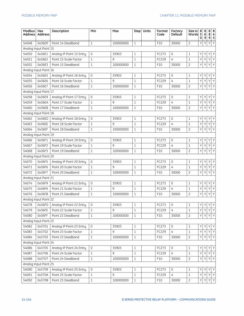
MODBUS MEMORY MAP CHAPTER 11: MODBUS MEMORY MAP
54048 0x36DF Point 14 Deadband 1 100000000 1 F10 30000 2 Y Y Y Y
Analog Input Point 15
54050 0x36E1 Analog IP Point 15 Entry 0 35903 1 FC273 0 1 Y Y Y Y
54051 0x36E2 Point 15 Scale Factor 1 9 1 FC229 4 1 Y Y Y Y
54052 0x36E3 Point 15 Deadband 1 100000000 1 F10 30000 2 Y Y Y Y
Analog Input Point 16
54054 0x36E5 Analog IP Point 16 Entry 0 35903 1 FC273 0 1 Y Y Y Y
54055 0x36E6 Point 16 Scale Factor 1 9 1 FC229 4 1 Y Y Y Y
54056 0x36E7 Point 16 Deadband 1 100000000 1 F10 30000 2 Y Y Y Y
Analog Input Point 17
54058 0x36E9 Analog IP Point 17 Entry 0 35903 1 FC273 0 1 Y Y Y Y
54059 0x36EA Point 17 Scale Factor 1 9 1 FC229 4 1 Y Y Y Y
54060 0x36EB Point 17 Deadband 1 100000000 1 F10 30000 2 Y Y Y Y
Analog Input Point 18
54062 0x36ED Analog IP Point 18 Entry 0 35903 1 FC273 0 1 Y Y Y Y
54063 0x36EE Point 18 Scale Factor 1 9 1 FC229 4 1 Y Y Y Y
54064 0x36EF Point 18 Deadband 1 100000000 1 F10 30000 2 Y Y Y Y
Analog Input Point 19
54066 0x36F1 Analog IP Point 19 Entry 0 35903 1 FC273 0 1 Y Y Y Y
54067 0x36F2 Point 19 Scale Factor 1 9 1 FC229 4 1 Y Y Y Y
54068 0x36F3 Point 19 Deadband 1 100000000 1 F10 30000 2 Y Y Y Y
Analog Input Point 20
54070 0x36F5 Analog IP Point 20 Entry 0 35903 1 FC273 0 1 Y Y Y Y
54071 0x36F6 Point 20 Scale Factor 1 9 1 FC229 4 1 Y Y Y Y
54072 0x36F7 Point 20 Deadband 1 100000000 1 F10 30000 2 Y Y Y Y
Analog Input Point 21
54074 0x36F9 Analog IP Point 21 Entry 0 35903 1 FC273 0 1 Y Y Y Y
54075 0x36FA Point 21 Scale Factor 1 9 1 FC229 4 1 Y Y Y Y
54076 0x36FB Point 21 Deadband 1 100000000 1 F10 30000 2 Y Y Y Y
Analog Input Point 22
54078 0x36FD Analog IP Point 22 Entry 0 35903 1 FC273 0 1 Y Y Y Y
54079 0x36FE Point 22 Scale Factor 1 9 1 FC229 4 1 Y Y Y Y
54080 0x36FF Point 22 Deadband 1 100000000 1 F10 30000 2 Y Y Y Y
Analog Input Point 23
54082 0x3701 Analog IP Point 23 Entry 0 35903 1 FC273 0 1 Y Y Y Y
54083 0x3702 Point 23 Scale Factor 1 9 1 FC229 4 1 Y Y Y Y
54084 0x3703 Point 23 Deadband 1 100000000 1 F10 30000 2 Y Y Y Y
Analog Input Point 24
54086 0x3705 Analog IP Point 24 Entry 0 35903 1 FC273 0 1 Y Y Y Y
54087 0x3706 Point 24 Scale Factor 1 9 1 FC229 4 1 Y Y Y Y
54088 0x3707 Point 24 Deadband 1 100000000 1 F10 30000 2 Y Y Y Y
Analog Input Point 25
54090 0x3709 Analog IP Point 25 Entry 0 35903 1 FC273 0 1 Y Y Y Y
54091 0x370A Point 25 Scale Factor 1 9 1 FC229 4 1 Y Y Y Y
54092 0x370B Point 25 Deadband 1 100000000 1 F10 30000 2 Y Y Y Y
Modbus Address
Hex Address
Description Min Max Step Units Format Code
Factory Default
Size in Words
850
869
889
845
11-114 8 SERIES PROTECTIVE RELAY PLATFORM – COMMUNICATIONS GUIDE

CHAPTER 11: MODBUS MEMORY MAP MODBUS MEMORY MAP
Analog Input Point 26
54094 0x370D Analog IP Point 26 Entry 0 35903 1 FC273 0 1 Y Y Y Y
54095 0x370E Point 26 Scale Factor 1 9 1 FC229 4 1 Y Y Y Y
54096 0x370F Point 26 Deadband 1 100000000 1 F10 30000 2 Y Y Y Y
Analog Input Point 27
54098 0x3711 Analog IP Point 27 Entry 0 35903 1 FC273 0 1 Y Y Y Y
54099 0x3712 Point 27 Scale Factor 1 9 1 FC229 4 1 Y Y Y Y
54100 0x3713 Point 27 Deadband 1 100000000 1 F10 30000 2 Y Y Y Y
Analog Input Point 28
54102 0x3715 Analog IP Point 28 Entry 0 35903 1 FC273 0 1 Y Y Y Y
54103 0x3716 Point 28 Scale Factor 1 9 1 FC229 4 1 Y Y Y Y
54104 0x3717 Point 28 Deadband 1 100000000 1 F10 30000 2 Y Y Y Y
Analog Input Point 29
54106 0x3719 Analog IP Point 29 Entry 0 35903 1 FC273 0 1 Y Y Y Y
54107 0x371A Point 29 Scale Factor 1 9 1 FC229 4 1 Y Y Y Y
54108 0x371B Point 29 Deadband 1 100000000 1 F10 30000 2 Y Y Y Y
Analog Input Point 30
54110 0x371D Analog IP Point 30 Entry 0 35903 1 FC273 0 1 Y Y Y Y
54111 0x371E Point 30 Scale Factor 1 9 1 FC229 4 1 Y Y Y Y
54112 0x371F Point 30 Deadband 1 100000000 1 F10 30000 2 Y Y Y Y
Analog Input Point 31
54114 0x3721 Analog IP Point 31 Entry 0 35903 1 FC273 0 1 Y Y Y Y
54115 0x3722 Point 31 Scale Factor 1 9 1 FC229 4 1 Y Y Y Y
54116 0x3723 Point 31 Deadband 1 100000000 1 F10 30000 2 Y Y Y Y
Binary Output Point 0
54130 0x3731 Binary Output Point 0 ON 0 143 1 FC230 0 1 Y Y Y Y
54131 0x3732 Binary Output Point 0 OFF 0 143 1 FC230 0 1 Y Y Y Y
Binary Output Point 1
54132 0x3733 Binary Output Point 1 ON 0 143 1 FC230 0 1 Y Y Y Y
54133 0x3734 Binary Output Point 1 OFF 0 143 1 FC230 0 1 Y Y Y Y
Binary Output Point 2
54134 0x3735 Binary Output Point 2 ON 0 143 1 FC230 0 1 Y Y Y Y
54135 0x3736 Binary Output Point 2 OFF 0 143 1 FC230 0 1 Y Y Y Y
Binary Output Point 3
54136 0x3737 Binary Output Point 3 ON 0 143 1 FC230 0 1 Y Y Y Y
54137 0x3738 Binary Output Point 3 OFF 0 143 1 FC230 0 1 Y Y Y Y
Binary Output Point 4
54138 0x3739 Binary Output Point 4 ON 0 143 1 FC230 0 1 Y Y Y Y
54139 0x373A Binary Output Point 4 OFF 0 143 1 FC230 0 1 Y Y Y Y
Binary Output Point 5
54140 0x373B Binary Output Point 5 ON 0 143 1 FC230 0 1 Y Y Y Y
54141 0x373C Binary Output Point 5 OFF 0 143 1 FC230 0 1 Y Y Y Y
Binary Output Point 6
54142 0x373D Binary Output Point 6 ON 0 143 1 FC230 0 1 Y Y Y Y
54143 0x373E Binary Output Point 6 OFF 0 143 1 FC230 0 1 Y Y Y Y
Modbus Address
Hex Address
Description Min Max Step Units Format Code
Factory Default
Size in Words
850
869
889
845
8 SERIES PROTECTIVE RELAY PLATFORM – COMMUNICATIONS GUIDE 11-115
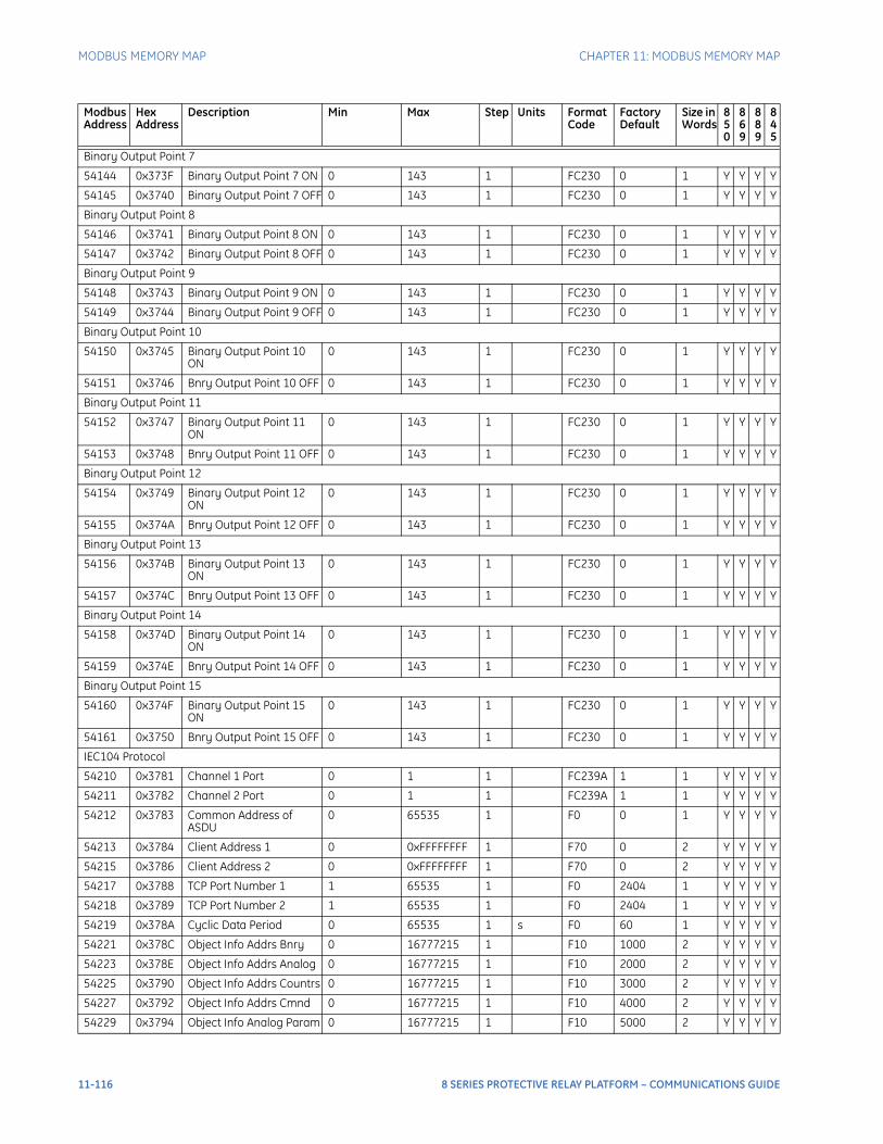
MODBUS MEMORY MAP CHAPTER 11: MODBUS MEMORY MAP
Binary Output Point 7
54144 0x373F Binary Output Point 7 ON 0 143 1 FC230 0 1 Y Y Y Y
54145 0x3740 Binary Output Point 7 OFF 0 143 1 FC230 0 1 Y Y Y Y
Binary Output Point 8
54146 0x3741 Binary Output Point 8 ON 0 143 1 FC230 0 1 Y Y Y Y
54147 0x3742 Binary Output Point 8 OFF 0 143 1 FC230 0 1 Y Y Y Y
Binary Output Point 9
54148 0x3743 Binary Output Point 9 ON 0 143 1 FC230 0 1 Y Y Y Y
54149 0x3744 Binary Output Point 9 OFF 0 143 1 FC230 0 1 Y Y Y Y
Binary Output Point 10
54150 0x3745 Binary Output Point 10 ON
0 143 1 FC230 0 1 Y Y Y Y
54151 0x3746 Bnry Output Point 10 OFF 0 143 1 FC230 0 1 Y Y Y Y
Binary Output Point 11
54152 0x3747 Binary Output Point 11 ON
0 143 1 FC230 0 1 Y Y Y Y
54153 0x3748 Bnry Output Point 11 OFF 0 143 1 FC230 0 1 Y Y Y Y
Binary Output Point 12
54154 0x3749 Binary Output Point 12 ON
0 143 1 FC230 0 1 Y Y Y Y
54155 0x374A Bnry Output Point 12 OFF 0 143 1 FC230 0 1 Y Y Y Y
Binary Output Point 13
54156 0x374B Binary Output Point 13 ON
0 143 1 FC230 0 1 Y Y Y Y
54157 0x374C Bnry Output Point 13 OFF 0 143 1 FC230 0 1 Y Y Y Y
Binary Output Point 14
54158 0x374D Binary Output Point 14 ON
0 143 1 FC230 0 1 Y Y Y Y
54159 0x374E Bnry Output Point 14 OFF 0 143 1 FC230 0 1 Y Y Y Y
Binary Output Point 15
54160 0x374F Binary Output Point 15 ON
0 143 1 FC230 0 1 Y Y Y Y
54161 0x3750 Bnry Output Point 15 OFF 0 143 1 FC230 0 1 Y Y Y Y
IEC104 Protocol
54210 0x3781 Channel 1 Port 0 1 1 FC239A 1 1 Y Y Y Y
54211 0x3782 Channel 2 Port 0 1 1 FC239A 1 1 Y Y Y Y
54212 0x3783 Common Address of ASDU
0 65535 1 F0 0 1 Y Y Y Y
54213 0x3784 Client Address 1 0 0xFFFFFFFF 1 F70 0 2 Y Y Y Y
54215 0x3786 Client Address 2 0 0xFFFFFFFF 1 F70 0 2 Y Y Y Y
54217 0x3788 TCP Port Number 1 1 65535 1 F0 2404 1 Y Y Y Y
54218 0x3789 TCP Port Number 2 1 65535 1 F0 2404 1 Y Y Y Y
54219 0x378A Cyclic Data Period 0 65535 1 s F0 60 1 Y Y Y Y
54221 0x378C Object Info Addrs Bnry 0 16777215 1 F10 1000 2 Y Y Y Y
54223 0x378E Object Info Addrs Analog 0 16777215 1 F10 2000 2 Y Y Y Y
54225 0x3790 Object Info Addrs Countrs 0 16777215 1 F10 3000 2 Y Y Y Y
54227 0x3792 Object Info Addrs Cmnd 0 16777215 1 F10 4000 2 Y Y Y Y
54229 0x3794 Object Info Analog Param 0 16777215 1 F10 5000 2 Y Y Y Y
Modbus Address
Hex Address
Description Min Max Step Units Format Code
Factory Default
Size in Words
850
869
889
845
11-116 8 SERIES PROTECTIVE RELAY PLATFORM – COMMUNICATIONS GUIDE
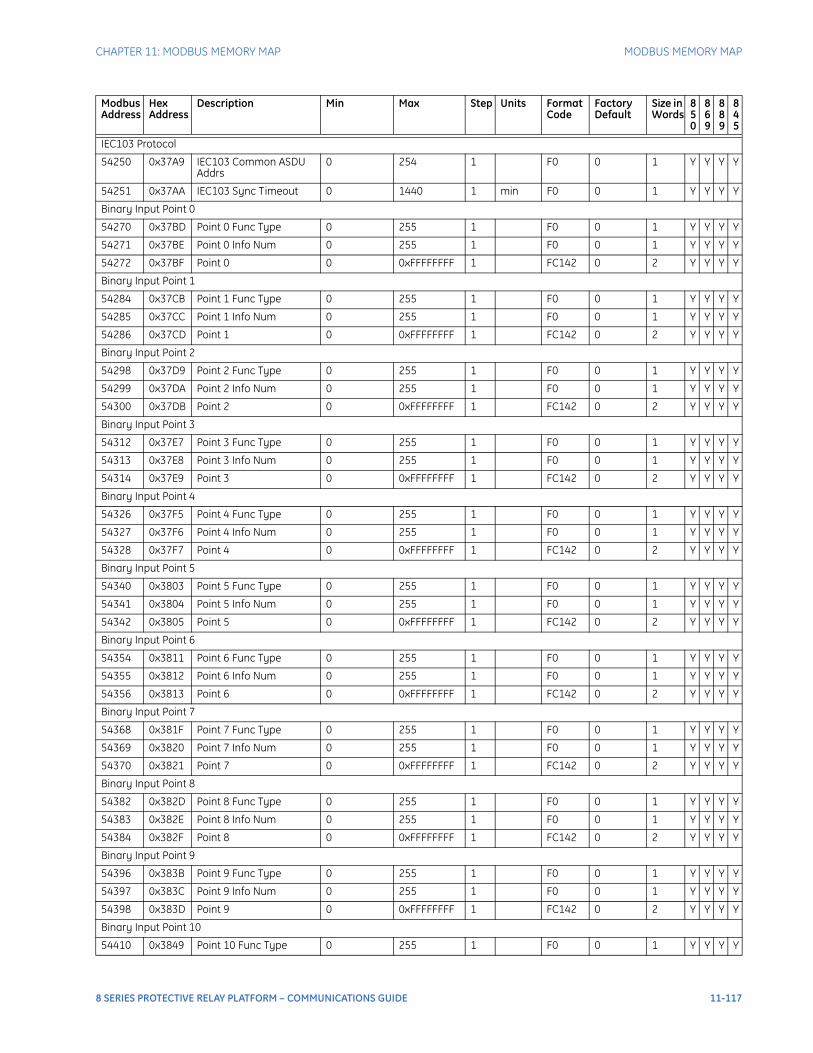
CHAPTER 11: MODBUS MEMORY MAP MODBUS MEMORY MAP
IEC103 Protocol
54250 0x37A9 IEC103 Common ASDU Addrs
0 254 1 F0 0 1 Y Y Y Y
54251 0x37AA IEC103 Sync Timeout 0 1440 1 min F0 0 1 Y Y Y Y
Binary Input Point 0
54270 0x37BD Point 0 Func Type 0 255 1 F0 0 1 Y Y Y Y
54271 0x37BE Point 0 Info Num 0 255 1 F0 0 1 Y Y Y Y
54272 0x37BF Point 0 0 0xFFFFFFFF 1 FC142 0 2 Y Y Y Y
Binary Input Point 1
54284 0x37CB Point 1 Func Type 0 255 1 F0 0 1 Y Y Y Y
54285 0x37CC Point 1 Info Num 0 255 1 F0 0 1 Y Y Y Y
54286 0x37CD Point 1 0 0xFFFFFFFF 1 FC142 0 2 Y Y Y Y
Binary Input Point 2
54298 0x37D9 Point 2 Func Type 0 255 1 F0 0 1 Y Y Y Y
54299 0x37DA Point 2 Info Num 0 255 1 F0 0 1 Y Y Y Y
54300 0x37DB Point 2 0 0xFFFFFFFF 1 FC142 0 2 Y Y Y Y
Binary Input Point 3
54312 0x37E7 Point 3 Func Type 0 255 1 F0 0 1 Y Y Y Y
54313 0x37E8 Point 3 Info Num 0 255 1 F0 0 1 Y Y Y Y
54314 0x37E9 Point 3 0 0xFFFFFFFF 1 FC142 0 2 Y Y Y Y
Binary Input Point 4
54326 0x37F5 Point 4 Func Type 0 255 1 F0 0 1 Y Y Y Y
54327 0x37F6 Point 4 Info Num 0 255 1 F0 0 1 Y Y Y Y
54328 0x37F7 Point 4 0 0xFFFFFFFF 1 FC142 0 2 Y Y Y Y
Binary Input Point 5
54340 0x3803 Point 5 Func Type 0 255 1 F0 0 1 Y Y Y Y
54341 0x3804 Point 5 Info Num 0 255 1 F0 0 1 Y Y Y Y
54342 0x3805 Point 5 0 0xFFFFFFFF 1 FC142 0 2 Y Y Y Y
Binary Input Point 6
54354 0x3811 Point 6 Func Type 0 255 1 F0 0 1 Y Y Y Y
54355 0x3812 Point 6 Info Num 0 255 1 F0 0 1 Y Y Y Y
54356 0x3813 Point 6 0 0xFFFFFFFF 1 FC142 0 2 Y Y Y Y
Binary Input Point 7
54368 0x381F Point 7 Func Type 0 255 1 F0 0 1 Y Y Y Y
54369 0x3820 Point 7 Info Num 0 255 1 F0 0 1 Y Y Y Y
54370 0x3821 Point 7 0 0xFFFFFFFF 1 FC142 0 2 Y Y Y Y
Binary Input Point 8
54382 0x382D Point 8 Func Type 0 255 1 F0 0 1 Y Y Y Y
54383 0x382E Point 8 Info Num 0 255 1 F0 0 1 Y Y Y Y
54384 0x382F Point 8 0 0xFFFFFFFF 1 FC142 0 2 Y Y Y Y
Binary Input Point 9
54396 0x383B Point 9 Func Type 0 255 1 F0 0 1 Y Y Y Y
54397 0x383C Point 9 Info Num 0 255 1 F0 0 1 Y Y Y Y
54398 0x383D Point 9 0 0xFFFFFFFF 1 FC142 0 2 Y Y Y Y
Binary Input Point 10
54410 0x3849 Point 10 Func Type 0 255 1 F0 0 1 Y Y Y Y
Modbus Address
Hex Address
Description Min Max Step Units Format Code
Factory Default
Size in Words
850
869
889
845
8 SERIES PROTECTIVE RELAY PLATFORM – COMMUNICATIONS GUIDE 11-117
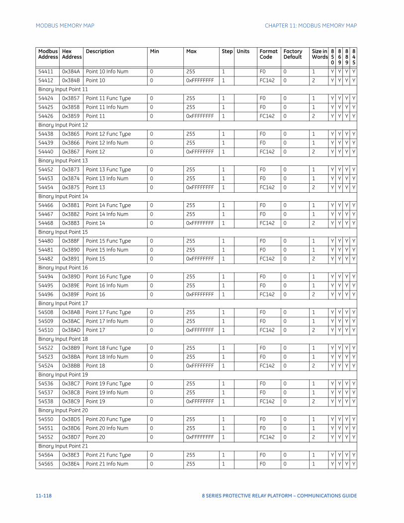
MODBUS MEMORY MAP CHAPTER 11: MODBUS MEMORY MAP
54411 0x384A Point 10 Info Num 0 255 1 F0 0 1 Y Y Y Y
54412 0x384B Point 10 0 0xFFFFFFFF 1 FC142 0 2 Y Y Y Y
Binary Input Point 11
54424 0x3857 Point 11 Func Type 0 255 1 F0 0 1 Y Y Y Y
54425 0x3858 Point 11 Info Num 0 255 1 F0 0 1 Y Y Y Y
54426 0x3859 Point 11 0 0xFFFFFFFF 1 FC142 0 2 Y Y Y Y
Binary Input Point 12
54438 0x3865 Point 12 Func Type 0 255 1 F0 0 1 Y Y Y Y
54439 0x3866 Point 12 Info Num 0 255 1 F0 0 1 Y Y Y Y
54440 0x3867 Point 12 0 0xFFFFFFFF 1 FC142 0 2 Y Y Y Y
Binary Input Point 13
54452 0x3873 Point 13 Func Type 0 255 1 F0 0 1 Y Y Y Y
54453 0x3874 Point 13 Info Num 0 255 1 F0 0 1 Y Y Y Y
54454 0x3875 Point 13 0 0xFFFFFFFF 1 FC142 0 2 Y Y Y Y
Binary Input Point 14
54466 0x3881 Point 14 Func Type 0 255 1 F0 0 1 Y Y Y Y
54467 0x3882 Point 14 Info Num 0 255 1 F0 0 1 Y Y Y Y
54468 0x3883 Point 14 0 0xFFFFFFFF 1 FC142 0 2 Y Y Y Y
Binary Input Point 15
54480 0x388F Point 15 Func Type 0 255 1 F0 0 1 Y Y Y Y
54481 0x3890 Point 15 Info Num 0 255 1 F0 0 1 Y Y Y Y
54482 0x3891 Point 15 0 0xFFFFFFFF 1 FC142 0 2 Y Y Y Y
Binary Input Point 16
54494 0x389D Point 16 Func Type 0 255 1 F0 0 1 Y Y Y Y
54495 0x389E Point 16 Info Num 0 255 1 F0 0 1 Y Y Y Y
54496 0x389F Point 16 0 0xFFFFFFFF 1 FC142 0 2 Y Y Y Y
Binary Input Point 17
54508 0x38AB Point 17 Func Type 0 255 1 F0 0 1 Y Y Y Y
54509 0x38AC Point 17 Info Num 0 255 1 F0 0 1 Y Y Y Y
54510 0x38AD Point 17 0 0xFFFFFFFF 1 FC142 0 2 Y Y Y Y
Binary Input Point 18
54522 0x38B9 Point 18 Func Type 0 255 1 F0 0 1 Y Y Y Y
54523 0x38BA Point 18 Info Num 0 255 1 F0 0 1 Y Y Y Y
54524 0x38BB Point 18 0 0xFFFFFFFF 1 FC142 0 2 Y Y Y Y
Binary Input Point 19
54536 0x38C7 Point 19 Func Type 0 255 1 F0 0 1 Y Y Y Y
54537 0x38C8 Point 19 Info Num 0 255 1 F0 0 1 Y Y Y Y
54538 0x38C9 Point 19 0 0xFFFFFFFF 1 FC142 0 2 Y Y Y Y
Binary Input Point 20
54550 0x38D5 Point 20 Func Type 0 255 1 F0 0 1 Y Y Y Y
54551 0x38D6 Point 20 Info Num 0 255 1 F0 0 1 Y Y Y Y
54552 0x38D7 Point 20 0 0xFFFFFFFF 1 FC142 0 2 Y Y Y Y
Binary Input Point 21
54564 0x38E3 Point 21 Func Type 0 255 1 F0 0 1 Y Y Y Y
54565 0x38E4 Point 21 Info Num 0 255 1 F0 0 1 Y Y Y Y
Modbus Address
Hex Address
Description Min Max Step Units Format Code
Factory Default
Size in Words
850
869
889
845
11-118 8 SERIES PROTECTIVE RELAY PLATFORM – COMMUNICATIONS GUIDE

CHAPTER 11: MODBUS MEMORY MAP MODBUS MEMORY MAP
54566 0x38E5 Point 21 0 0xFFFFFFFF 1 FC142 0 2 Y Y Y Y
Binary Input Point 22
54578 0x38F1 Point 22 Func Type 0 255 1 F0 0 1 Y Y Y Y
54579 0x38F2 Point 22 Info Num 0 255 1 F0 0 1 Y Y Y Y
54580 0x38F3 Point 22 0 0xFFFFFFFF 1 FC142 0 2 Y Y Y Y
Binary Input Point 23
54592 0x38FF Point 23 Func Type 0 255 1 F0 0 1 Y Y Y Y
54593 0x3900 Point 23 Info Num 0 255 1 F0 0 1 Y Y Y Y
54594 0x3901 Point 23 0 0xFFFFFFFF 1 FC142 0 2 Y Y Y Y
Binary Input Point 24
54606 0x390D Point 24 Func Type 0 255 1 F0 0 1 Y Y Y Y
54607 0x390E Point 24 Info Num 0 255 1 F0 0 1 Y Y Y Y
54608 0x390F Point 24 0 0xFFFFFFFF 1 FC142 0 2 Y Y Y Y
Binary Input Point 25
54620 0x391B Point 25 Func Type 0 255 1 F0 0 1 Y Y Y Y
54621 0x391C Point 25 Info Num 0 255 1 F0 0 1 Y Y Y Y
54622 0x391D Point 25 0 0xFFFFFFFF 1 FC142 0 2 Y Y Y Y
Binary Input Point 26
54634 0x3929 Point 26 Func Type 0 255 1 F0 0 1 Y Y Y Y
54635 0x392A Point 26 Info Num 0 255 1 F0 0 1 Y Y Y Y
54636 0x392B Point 26 0 0xFFFFFFFF 1 FC142 0 2 Y Y Y Y
Binary Input Point 27
54648 0x3937 Point 27 Func Type 0 255 1 F0 0 1 Y Y Y Y
54649 0x3938 Point 27 Info Num 0 255 1 F0 0 1 Y Y Y Y
54650 0x3939 Point 27 0 0xFFFFFFFF 1 FC142 0 2 Y Y Y Y
Binary Input Point 28
54662 0x3945 Point 28 Func Type 0 255 1 F0 0 1 Y Y Y Y
54663 0x3946 Point 28 Info Num 0 255 1 F0 0 1 Y Y Y Y
54664 0x3947 Point 28 0 0xFFFFFFFF 1 FC142 0 2 Y Y Y Y
Binary Input Point 29
54676 0x3953 Point 29 Func Type 0 255 1 F0 0 1 Y Y Y Y
54677 0x3954 Point 29 Info Num 0 255 1 F0 0 1 Y Y Y Y
54678 0x3955 Point 29 0 0xFFFFFFFF 1 FC142 0 2 Y Y Y Y
Binary Input Point 30
54690 0x3961 Point 30 Func Type 0 255 1 F0 0 1 Y Y Y Y
54691 0x3962 Point 30 Info Num 0 255 1 F0 0 1 Y Y Y Y
54692 0x3963 Point 30 0 0xFFFFFFFF 1 FC142 0 2 Y Y Y Y
Binary Input Point 31
54704 0x396F Point 31 Func Type 0 255 1 F0 0 1 Y Y Y Y
54705 0x3970 Point 31 Info Num 0 255 1 F0 0 1 Y Y Y Y
54706 0x3971 Point 31 0 0xFFFFFFFF 1 FC142 0 2 Y Y Y Y
Binary Input Point 32
54718 0x397D Point 32 Func Type 0 255 1 F0 0 1 Y Y Y Y
54719 0x397E Point 32 Info Num 0 255 1 F0 0 1 Y Y Y Y
54720 0x397F Point 32 0 0xFFFFFFFF 1 FC142 0 2 Y Y Y Y
Modbus Address
Hex Address
Description Min Max Step Units Format Code
Factory Default
Size in Words
850
869
889
845
8 SERIES PROTECTIVE RELAY PLATFORM – COMMUNICATIONS GUIDE 11-119

MODBUS MEMORY MAP CHAPTER 11: MODBUS MEMORY MAP
Binary Input Point 33
54732 0x398B Point 33 Func Type 0 255 1 F0 0 1 Y Y Y Y
54733 0x398C Point 33 Info Num 0 255 1 F0 0 1 Y Y Y Y
54734 0x398D Point 33 0 0xFFFFFFFF 1 FC142 0 2 Y Y Y Y
Binary Input Point 34
54746 0x3999 Point 34 Func Type 0 255 1 F0 0 1 Y Y Y Y
54747 0x399A Point 34 Info Num 0 255 1 F0 0 1 Y Y Y Y
54748 0x399B Point 34 0 0xFFFFFFFF 1 FC142 0 2 Y Y Y Y
Binary Input Point 35
54760 0x39A7 Point 35 Func Type 0 255 1 F0 0 1 Y Y Y Y
54761 0x39A8 Point 35 Info Num 0 255 1 F0 0 1 Y Y Y Y
54762 0x39A9 Point 35 0 0xFFFFFFFF 1 FC142 0 2 Y Y Y Y
Binary Input Point 36
54774 0x39B5 Point 36 Func Type 0 255 1 F0 0 1 Y Y Y Y
54775 0x39B6 Point 36 Info Num 0 255 1 F0 0 1 Y Y Y Y
54776 0x39B7 Point 36 0 0xFFFFFFFF 1 FC142 0 2 Y Y Y Y
Binary Input Point 37
54788 0x39C3 Point 37 Func Type 0 255 1 F0 0 1 Y Y Y Y
54789 0x39C4 Point 37 Info Num 0 255 1 F0 0 1 Y Y Y Y
54790 0x39C5 Point 37 0 0xFFFFFFFF 1 FC142 0 2 Y Y Y Y
Binary Input Point 38
54802 0x39D1 Point 38 Func Type 0 255 1 F0 0 1 Y Y Y Y
54803 0x39D2 Point 38 Info Num 0 255 1 F0 0 1 Y Y Y Y
54804 0x39D3 Point 38 0 0xFFFFFFFF 1 FC142 0 2 Y Y Y Y
Binary Input Point 39
54816 0x39DF Point 39 Func Type 0 255 1 F0 0 1 Y Y Y Y
54817 0x39E0 Point 39 Info Num 0 255 1 F0 0 1 Y Y Y Y
54818 0x39E1 Point 39 0 0xFFFFFFFF 1 FC142 0 2 Y Y Y Y
Binary Input Point 40
54830 0x39ED Point 40 Func Type 0 255 1 F0 0 1 Y Y Y Y
54831 0x39EE Point 40 Info Num 0 255 1 F0 0 1 Y Y Y Y
54832 0x39EF Point 40 0 0xFFFFFFFF 1 FC142 0 2 Y Y Y Y
Binary Input Point 41
54844 0x39FB Point 41 Func Type 0 255 1 F0 0 1 Y Y Y Y
54845 0x39FC Point 41 Info Num 0 255 1 F0 0 1 Y Y Y Y
54846 0x39FD Point 41 0 0xFFFFFFFF 1 FC142 0 2 Y Y Y Y
Binary Input Point 42
54858 0x3A09 Point 42 Func Type 0 255 1 F0 0 1 Y Y Y Y
54859 0x3A0A Point 42 Info Num 0 255 1 F0 0 1 Y Y Y Y
54860 0x3A0B Point 42 0 0xFFFFFFFF 1 FC142 0 2 Y Y Y Y
Binary Input Point 43
54872 0x3A17 Point 43 Func Type 0 255 1 F0 0 1 Y Y Y Y
54873 0x3A18 Point 43 Info Num 0 255 1 F0 0 1 Y Y Y Y
54874 0x3A19 Point 43 0 0xFFFFFFFF 1 FC142 0 2 Y Y Y Y
Binary Input Point 44
Modbus Address
Hex Address
Description Min Max Step Units Format Code
Factory Default
Size in Words
850
869
889
845
11-120 8 SERIES PROTECTIVE RELAY PLATFORM – COMMUNICATIONS GUIDE
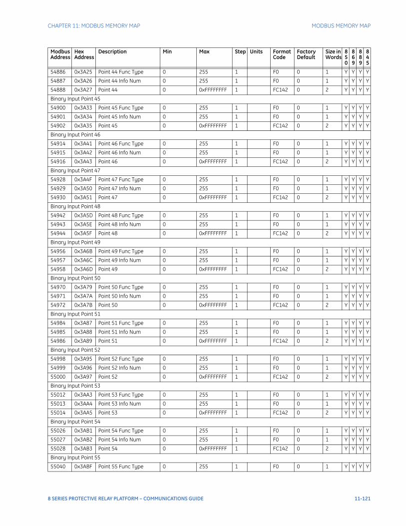
CHAPTER 11: MODBUS MEMORY MAP MODBUS MEMORY MAP
54886 0x3A25 Point 44 Func Type 0 255 1 F0 0 1 Y Y Y Y
54887 0x3A26 Point 44 Info Num 0 255 1 F0 0 1 Y Y Y Y
54888 0x3A27 Point 44 0 0xFFFFFFFF 1 FC142 0 2 Y Y Y Y
Binary Input Point 45
54900 0x3A33 Point 45 Func Type 0 255 1 F0 0 1 Y Y Y Y
54901 0x3A34 Point 45 Info Num 0 255 1 F0 0 1 Y Y Y Y
54902 0x3A35 Point 45 0 0xFFFFFFFF 1 FC142 0 2 Y Y Y Y
Binary Input Point 46
54914 0x3A41 Point 46 Func Type 0 255 1 F0 0 1 Y Y Y Y
54915 0x3A42 Point 46 Info Num 0 255 1 F0 0 1 Y Y Y Y
54916 0x3A43 Point 46 0 0xFFFFFFFF 1 FC142 0 2 Y Y Y Y
Binary Input Point 47
54928 0x3A4F Point 47 Func Type 0 255 1 F0 0 1 Y Y Y Y
54929 0x3A50 Point 47 Info Num 0 255 1 F0 0 1 Y Y Y Y
54930 0x3A51 Point 47 0 0xFFFFFFFF 1 FC142 0 2 Y Y Y Y
Binary Input Point 48
54942 0x3A5D Point 48 Func Type 0 255 1 F0 0 1 Y Y Y Y
54943 0x3A5E Point 48 Info Num 0 255 1 F0 0 1 Y Y Y Y
54944 0x3A5F Point 48 0 0xFFFFFFFF 1 FC142 0 2 Y Y Y Y
Binary Input Point 49
54956 0x3A6B Point 49 Func Type 0 255 1 F0 0 1 Y Y Y Y
54957 0x3A6C Point 49 Info Num 0 255 1 F0 0 1 Y Y Y Y
54958 0x3A6D Point 49 0 0xFFFFFFFF 1 FC142 0 2 Y Y Y Y
Binary Input Point 50
54970 0x3A79 Point 50 Func Type 0 255 1 F0 0 1 Y Y Y Y
54971 0x3A7A Point 50 Info Num 0 255 1 F0 0 1 Y Y Y Y
54972 0x3A7B Point 50 0 0xFFFFFFFF 1 FC142 0 2 Y Y Y Y
Binary Input Point 51
54984 0x3A87 Point 51 Func Type 0 255 1 F0 0 1 Y Y Y Y
54985 0x3A88 Point 51 Info Num 0 255 1 F0 0 1 Y Y Y Y
54986 0x3A89 Point 51 0 0xFFFFFFFF 1 FC142 0 2 Y Y Y Y
Binary Input Point 52
54998 0x3A95 Point 52 Func Type 0 255 1 F0 0 1 Y Y Y Y
54999 0x3A96 Point 52 Info Num 0 255 1 F0 0 1 Y Y Y Y
55000 0x3A97 Point 52 0 0xFFFFFFFF 1 FC142 0 2 Y Y Y Y
Binary Input Point 53
55012 0x3AA3 Point 53 Func Type 0 255 1 F0 0 1 Y Y Y Y
55013 0x3AA4 Point 53 Info Num 0 255 1 F0 0 1 Y Y Y Y
55014 0x3AA5 Point 53 0 0xFFFFFFFF 1 FC142 0 2 Y Y Y Y
Binary Input Point 54
55026 0x3AB1 Point 54 Func Type 0 255 1 F0 0 1 Y Y Y Y
55027 0x3AB2 Point 54 Info Num 0 255 1 F0 0 1 Y Y Y Y
55028 0x3AB3 Point 54 0 0xFFFFFFFF 1 FC142 0 2 Y Y Y Y
Binary Input Point 55
55040 0x3ABF Point 55 Func Type 0 255 1 F0 0 1 Y Y Y Y
Modbus Address
Hex Address
Description Min Max Step Units Format Code
Factory Default
Size in Words
850
869
889
845
8 SERIES PROTECTIVE RELAY PLATFORM – COMMUNICATIONS GUIDE 11-121

MODBUS MEMORY MAP CHAPTER 11: MODBUS MEMORY MAP
55041 0x3AC0 Point 55 Info Num 0 255 1 F0 0 1 Y Y Y Y
55042 0x3AC1 Point 55 0 0xFFFFFFFF 1 FC142 0 2 Y Y Y Y
Binary Input Point 56
55054 0x3ACD Point 56 Func Type 0 255 1 F0 0 1 Y Y Y Y
55055 0x3ACE Point 56 Info Num 0 255 1 F0 0 1 Y Y Y Y
55056 0x3ACF Point 56 0 0xFFFFFFFF 1 FC142 0 2 Y Y Y Y
Binary Input Point 57
55068 0x3ADB Point 57 Func Type 0 255 1 F0 0 1 Y Y Y Y
55069 0x3ADC Point 57 Info Num 0 255 1 F0 0 1 Y Y Y Y
55070 0x3ADD Point 57 0 0xFFFFFFFF 1 FC142 0 2 Y Y Y Y
Binary Input Point 58
55082 0x3AE9 Point 58 Func Type 0 255 1 F0 0 1 Y Y Y Y
55083 0x3AEA Point 58 Info Num 0 255 1 F0 0 1 Y Y Y Y
55084 0x3AEB Point 58 0 0xFFFFFFFF 1 FC142 0 2 Y Y Y Y
Binary Input Point 59
55096 0x3AF7 Point 59 Func Type 0 255 1 F0 0 1 Y Y Y Y
55097 0x3AF8 Point 59 Info Num 0 255 1 F0 0 1 Y Y Y Y
55098 0x3AF9 Point 59 0 0xFFFFFFFF 1 FC142 0 2 Y Y Y Y
Binary Input Point 60
55110 0x3B05 Point 60 Func Type 0 255 1 F0 0 1 Y Y Y Y
55111 0x3B06 Point 60 Info Num 0 255 1 F0 0 1 Y Y Y Y
55112 0x3B07 Point 60 0 0xFFFFFFFF 1 FC142 0 2 Y Y Y Y
Binary Input Point 61
55124 0x3B13 Point 61 Func Type 0 255 1 F0 0 1 Y Y Y Y
55125 0x3B14 Point 61 Info Num 0 255 1 F0 0 1 Y Y Y Y
55126 0x3B15 Point 61 0 0xFFFFFFFF 1 FC142 0 2 Y Y Y Y
Binary Input Point 62
55138 0x3B21 Point 62 Func Type 0 255 1 F0 0 1 Y Y Y Y
55139 0x3B22 Point 62 Info Num 0 255 1 F0 0 1 Y Y Y Y
55140 0x3B23 Point 62 0 0xFFFFFFFF 1 FC142 0 2 Y Y Y Y
Binary Input Point 63
55152 0x3B2F Point 63 Func Type 0 255 1 F0 0 1 Y Y Y Y
55153 0x3B30 Point 63 Info Num 0 255 1 F0 0 1 Y Y Y Y
55154 0x3B31 Point 63 0 0xFFFFFFFF 1 FC142 0 2 Y Y Y Y
Binary Input Point 64
55166 0x3B3D Point 64 Func Type 0 255 1 F0 0 1 Y Y Y Y
55167 0x3B3E Point 64 Info Num 0 255 1 F0 0 1 Y Y Y Y
55168 0x3B3F Point 64 0 0xFFFFFFFF 1 FC142 0 2 Y Y Y Y
Binary Input Point 65
55180 0x3B4B Point 65 Func Type 0 255 1 F0 0 1 Y Y Y Y
55181 0x3B4C Point 65 Info Num 0 255 1 F0 0 1 Y Y Y Y
55182 0x3B4D Point 65 0 0xFFFFFFFF 1 FC142 0 2 Y Y Y Y
Binary Input Point 66
55194 0x3B59 Point 66 Func Type 0 255 1 F0 0 1 Y Y Y Y
55195 0x3B5A Point 66 Info Num 0 255 1 F0 0 1 Y Y Y Y
Modbus Address
Hex Address
Description Min Max Step Units Format Code
Factory Default
Size in Words
850
869
889
845
11-122 8 SERIES PROTECTIVE RELAY PLATFORM – COMMUNICATIONS GUIDE
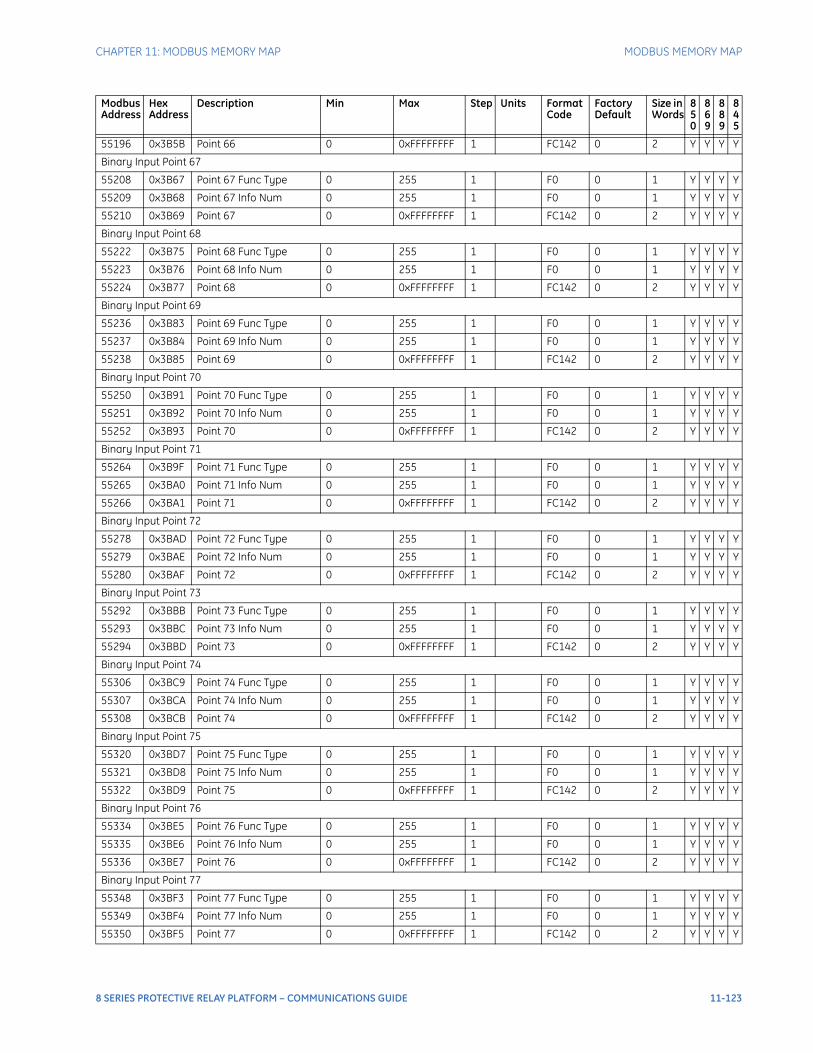
CHAPTER 11: MODBUS MEMORY MAP MODBUS MEMORY MAP
55196 0x3B5B Point 66 0 0xFFFFFFFF 1 FC142 0 2 Y Y Y Y
Binary Input Point 67
55208 0x3B67 Point 67 Func Type 0 255 1 F0 0 1 Y Y Y Y
55209 0x3B68 Point 67 Info Num 0 255 1 F0 0 1 Y Y Y Y
55210 0x3B69 Point 67 0 0xFFFFFFFF 1 FC142 0 2 Y Y Y Y
Binary Input Point 68
55222 0x3B75 Point 68 Func Type 0 255 1 F0 0 1 Y Y Y Y
55223 0x3B76 Point 68 Info Num 0 255 1 F0 0 1 Y Y Y Y
55224 0x3B77 Point 68 0 0xFFFFFFFF 1 FC142 0 2 Y Y Y Y
Binary Input Point 69
55236 0x3B83 Point 69 Func Type 0 255 1 F0 0 1 Y Y Y Y
55237 0x3B84 Point 69 Info Num 0 255 1 F0 0 1 Y Y Y Y
55238 0x3B85 Point 69 0 0xFFFFFFFF 1 FC142 0 2 Y Y Y Y
Binary Input Point 70
55250 0x3B91 Point 70 Func Type 0 255 1 F0 0 1 Y Y Y Y
55251 0x3B92 Point 70 Info Num 0 255 1 F0 0 1 Y Y Y Y
55252 0x3B93 Point 70 0 0xFFFFFFFF 1 FC142 0 2 Y Y Y Y
Binary Input Point 71
55264 0x3B9F Point 71 Func Type 0 255 1 F0 0 1 Y Y Y Y
55265 0x3BA0 Point 71 Info Num 0 255 1 F0 0 1 Y Y Y Y
55266 0x3BA1 Point 71 0 0xFFFFFFFF 1 FC142 0 2 Y Y Y Y
Binary Input Point 72
55278 0x3BAD Point 72 Func Type 0 255 1 F0 0 1 Y Y Y Y
55279 0x3BAE Point 72 Info Num 0 255 1 F0 0 1 Y Y Y Y
55280 0x3BAF Point 72 0 0xFFFFFFFF 1 FC142 0 2 Y Y Y Y
Binary Input Point 73
55292 0x3BBB Point 73 Func Type 0 255 1 F0 0 1 Y Y Y Y
55293 0x3BBC Point 73 Info Num 0 255 1 F0 0 1 Y Y Y Y
55294 0x3BBD Point 73 0 0xFFFFFFFF 1 FC142 0 2 Y Y Y Y
Binary Input Point 74
55306 0x3BC9 Point 74 Func Type 0 255 1 F0 0 1 Y Y Y Y
55307 0x3BCA Point 74 Info Num 0 255 1 F0 0 1 Y Y Y Y
55308 0x3BCB Point 74 0 0xFFFFFFFF 1 FC142 0 2 Y Y Y Y
Binary Input Point 75
55320 0x3BD7 Point 75 Func Type 0 255 1 F0 0 1 Y Y Y Y
55321 0x3BD8 Point 75 Info Num 0 255 1 F0 0 1 Y Y Y Y
55322 0x3BD9 Point 75 0 0xFFFFFFFF 1 FC142 0 2 Y Y Y Y
Binary Input Point 76
55334 0x3BE5 Point 76 Func Type 0 255 1 F0 0 1 Y Y Y Y
55335 0x3BE6 Point 76 Info Num 0 255 1 F0 0 1 Y Y Y Y
55336 0x3BE7 Point 76 0 0xFFFFFFFF 1 FC142 0 2 Y Y Y Y
Binary Input Point 77
55348 0x3BF3 Point 77 Func Type 0 255 1 F0 0 1 Y Y Y Y
55349 0x3BF4 Point 77 Info Num 0 255 1 F0 0 1 Y Y Y Y
55350 0x3BF5 Point 77 0 0xFFFFFFFF 1 FC142 0 2 Y Y Y Y
Modbus Address
Hex Address
Description Min Max Step Units Format Code
Factory Default
Size in Words
850
869
889
845
8 SERIES PROTECTIVE RELAY PLATFORM – COMMUNICATIONS GUIDE 11-123
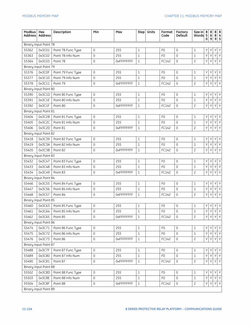
MODBUS MEMORY MAP CHAPTER 11: MODBUS MEMORY MAP
Binary Input Point 78
55362 0x3C01 Point 78 Func Type 0 255 1 F0 0 1 Y Y Y Y
55363 0x3C02 Point 78 Info Num 0 255 1 F0 0 1 Y Y Y Y
55364 0x3C03 Point 78 0 0xFFFFFFFF 1 FC142 0 2 Y Y Y Y
Binary Input Point 79
55376 0x3C0F Point 79 Func Type 0 255 1 F0 0 1 Y Y Y Y
55377 0x3C10 Point 79 Info Num 0 255 1 F0 0 1 Y Y Y Y
55378 0x3C11 Point 79 0 0xFFFFFFFF 1 FC142 0 2 Y Y Y Y
Binary Input Point 80
55390 0x3C1D Point 80 Func Type 0 255 1 F0 0 1 Y Y Y Y
55391 0x3C1E Point 80 Info Num 0 255 1 F0 0 1 Y Y Y Y
55392 0x3C1F Point 80 0 0xFFFFFFFF 1 FC142 0 2 Y Y Y Y
Binary Input Point 81
55404 0x3C2B Point 81 Func Type 0 255 1 F0 0 1 Y Y Y Y
55405 0x3C2C Point 81 Info Num 0 255 1 F0 0 1 Y Y Y Y
55406 0x3C2D Point 81 0 0xFFFFFFFF 1 FC142 0 2 Y Y Y Y
Binary Input Point 82
55418 0x3C39 Point 82 Func Type 0 255 1 F0 0 1 Y Y Y Y
55419 0x3C3A Point 82 Info Num 0 255 1 F0 0 1 Y Y Y Y
55420 0x3C3B Point 82 0 0xFFFFFFFF 1 FC142 0 2 Y Y Y Y
Binary Input Point 83
55432 0x3C47 Point 83 Func Type 0 255 1 F0 0 1 Y Y Y Y
55433 0x3C48 Point 83 Info Num 0 255 1 F0 0 1 Y Y Y Y
55434 0x3C49 Point 83 0 0xFFFFFFFF 1 FC142 0 2 Y Y Y Y
Binary Input Point 84
55446 0x3C55 Point 84 Func Type 0 255 1 F0 0 1 Y Y Y Y
55447 0x3C56 Point 84 Info Num 0 255 1 F0 0 1 Y Y Y Y
55448 0x3C57 Point 84 0 0xFFFFFFFF 1 FC142 0 2 Y Y Y Y
Binary Input Point 85
55460 0x3C63 Point 85 Func Type 0 255 1 F0 0 1 Y Y Y Y
55461 0x3C64 Point 85 Info Num 0 255 1 F0 0 1 Y Y Y Y
55462 0x3C65 Point 85 0 0xFFFFFFFF 1 FC142 0 2 Y Y Y Y
Binary Input Point 86
55474 0x3C71 Point 86 Func Type 0 255 1 F0 0 1 Y Y Y Y
55475 0x3C72 Point 86 Info Num 0 255 1 F0 0 1 Y Y Y Y
55476 0x3C73 Point 86 0 0xFFFFFFFF 1 FC142 0 2 Y Y Y Y
Binary Input Point 87
55488 0x3C7F Point 87 Func Type 0 255 1 F0 0 1 Y Y Y Y
55489 0x3C80 Point 87 Info Num 0 255 1 F0 0 1 Y Y Y Y
55490 0x3C81 Point 87 0 0xFFFFFFFF 1 FC142 0 2 Y Y Y Y
Binary Input Point 88
55502 0x3C8D Point 88 Func Type 0 255 1 F0 0 1 Y Y Y Y
55503 0x3C8E Point 88 Info Num 0 255 1 F0 0 1 Y Y Y Y
55504 0x3C8F Point 88 0 0xFFFFFFFF 1 FC142 0 2 Y Y Y Y
Binary Input Point 89
Modbus Address
Hex Address
Description Min Max Step Units Format Code
Factory Default
Size in Words
850
869
889
845
11-124 8 SERIES PROTECTIVE RELAY PLATFORM – COMMUNICATIONS GUIDE
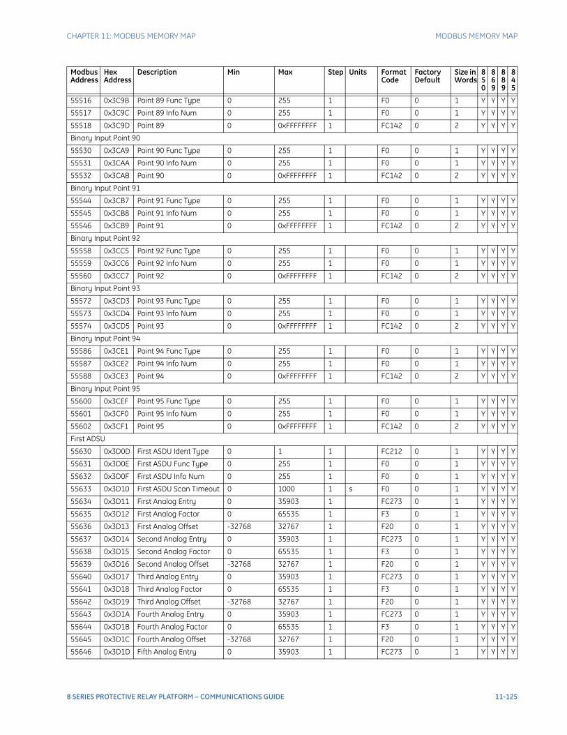
CHAPTER 11: MODBUS MEMORY MAP MODBUS MEMORY MAP
55516 0x3C9B Point 89 Func Type 0 255 1 F0 0 1 Y Y Y Y
55517 0x3C9C Point 89 Info Num 0 255 1 F0 0 1 Y Y Y Y
55518 0x3C9D Point 89 0 0xFFFFFFFF 1 FC142 0 2 Y Y Y Y
Binary Input Point 90
55530 0x3CA9 Point 90 Func Type 0 255 1 F0 0 1 Y Y Y Y
55531 0x3CAA Point 90 Info Num 0 255 1 F0 0 1 Y Y Y Y
55532 0x3CAB Point 90 0 0xFFFFFFFF 1 FC142 0 2 Y Y Y Y
Binary Input Point 91
55544 0x3CB7 Point 91 Func Type 0 255 1 F0 0 1 Y Y Y Y
55545 0x3CB8 Point 91 Info Num 0 255 1 F0 0 1 Y Y Y Y
55546 0x3CB9 Point 91 0 0xFFFFFFFF 1 FC142 0 2 Y Y Y Y
Binary Input Point 92
55558 0x3CC5 Point 92 Func Type 0 255 1 F0 0 1 Y Y Y Y
55559 0x3CC6 Point 92 Info Num 0 255 1 F0 0 1 Y Y Y Y
55560 0x3CC7 Point 92 0 0xFFFFFFFF 1 FC142 0 2 Y Y Y Y
Binary Input Point 93
55572 0x3CD3 Point 93 Func Type 0 255 1 F0 0 1 Y Y Y Y
55573 0x3CD4 Point 93 Info Num 0 255 1 F0 0 1 Y Y Y Y
55574 0x3CD5 Point 93 0 0xFFFFFFFF 1 FC142 0 2 Y Y Y Y
Binary Input Point 94
55586 0x3CE1 Point 94 Func Type 0 255 1 F0 0 1 Y Y Y Y
55587 0x3CE2 Point 94 Info Num 0 255 1 F0 0 1 Y Y Y Y
55588 0x3CE3 Point 94 0 0xFFFFFFFF 1 FC142 0 2 Y Y Y Y
Binary Input Point 95
55600 0x3CEF Point 95 Func Type 0 255 1 F0 0 1 Y Y Y Y
55601 0x3CF0 Point 95 Info Num 0 255 1 F0 0 1 Y Y Y Y
55602 0x3CF1 Point 95 0 0xFFFFFFFF 1 FC142 0 2 Y Y Y Y
First ADSU
55630 0x3D0D First ASDU Ident Type 0 1 1 FC212 0 1 Y Y Y Y
55631 0x3D0E First ASDU Func Type 0 255 1 F0 0 1 Y Y Y Y
55632 0x3D0F First ASDU Info Num 0 255 1 F0 0 1 Y Y Y Y
55633 0x3D10 First ASDU Scan Timeout 0 1000 1 s F0 0 1 Y Y Y Y
55634 0x3D11 First Analog Entry 0 35903 1 FC273 0 1 Y Y Y Y
55635 0x3D12 First Analog Factor 0 65535 1 F3 0 1 Y Y Y Y
55636 0x3D13 First Analog Offset -32768 32767 1 F20 0 1 Y Y Y Y
55637 0x3D14 Second Analog Entry 0 35903 1 FC273 0 1 Y Y Y Y
55638 0x3D15 Second Analog Factor 0 65535 1 F3 0 1 Y Y Y Y
55639 0x3D16 Second Analog Offset -32768 32767 1 F20 0 1 Y Y Y Y
55640 0x3D17 Third Analog Entry 0 35903 1 FC273 0 1 Y Y Y Y
55641 0x3D18 Third Analog Factor 0 65535 1 F3 0 1 Y Y Y Y
55642 0x3D19 Third Analog Offset -32768 32767 1 F20 0 1 Y Y Y Y
55643 0x3D1A Fourth Analog Entry 0 35903 1 FC273 0 1 Y Y Y Y
55644 0x3D1B Fourth Analog Factor 0 65535 1 F3 0 1 Y Y Y Y
55645 0x3D1C Fourth Analog Offset -32768 32767 1 F20 0 1 Y Y Y Y
55646 0x3D1D Fifth Analog Entry 0 35903 1 FC273 0 1 Y Y Y Y
Modbus Address
Hex Address
Description Min Max Step Units Format Code
Factory Default
Size in Words
850
869
889
845
8 SERIES PROTECTIVE RELAY PLATFORM – COMMUNICATIONS GUIDE 11-125
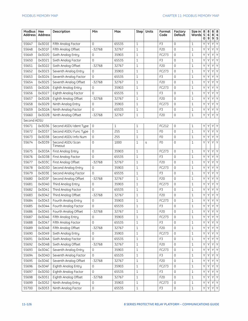
MODBUS MEMORY MAP CHAPTER 11: MODBUS MEMORY MAP
55647 0x3D1E Fifth Analog Factor 0 65535 1 F3 0 1 Y Y Y Y
55648 0x3D1F Fifth Analog Offset -32768 32767 1 F20 0 1 Y Y Y Y
55649 0x3D20 Sixth Analog Entry 0 35903 1 FC273 0 1 Y Y Y Y
55650 0x3D21 Sixth Analog Factor 0 65535 1 F3 0 1 Y Y Y Y
55651 0x3D22 Sixth Analog Offset -32768 32767 1 F20 0 1 Y Y Y Y
55652 0x3D23 Seventh Analog Entry 0 35903 1 FC273 0 1 Y Y Y Y
55653 0x3D24 Seventh Analog Factor 0 65535 1 F3 0 1 Y Y Y Y
55654 0x3D25 Seventh Analog Offset -32768 32767 1 F20 0 1 Y Y Y Y
55655 0x3D26 Eighth Analog Entry 0 35903 1 FC273 0 1 Y Y Y Y
55656 0x3D27 Eighth Analog Factor 0 65535 1 F3 0 1 Y Y Y Y
55657 0x3D28 Eighth Analog Offset -32768 32767 1 F20 0 1 Y Y Y Y
55658 0x3D29 Ninth Analog Entry 0 35903 1 FC273 0 1 Y Y Y Y
55659 0x3D2A Ninth Analog Factor 0 65535 1 F3 0 1 Y Y Y Y
55660 0x3D2B Ninth Analog Offset -32768 32767 1 F20 0 1 Y Y Y Y
Second ADSU
55671 0x3D36 Second ASDU Ident Type 0 1 1 FC212 0 1 Y Y Y Y
55672 0x3D37 Second ASDU Func Type 0 255 1 F0 0 1 Y Y Y Y
55673 0x3D38 Second ASDU Info Num 0 255 1 F0 0 1 Y Y Y Y
55674 0x3D39 Second ASDU Scan Timeout
0 1000 1 s F0 0 1 Y Y Y Y
55675 0x3D3A First Analog Entry 0 35903 1 FC273 0 1 Y Y Y Y
55676 0x3D3B First Analog Factor 0 65535 1 F3 0 1 Y Y Y Y
55677 0x3D3C First Analog Offset -32768 32767 1 F20 0 1 Y Y Y Y
55678 0x3D3D Second Analog Entry 0 35903 1 FC273 0 1 Y Y Y Y
55679 0x3D3E Second Analog Factor 0 65535 1 F3 0 1 Y Y Y Y
55680 0x3D3F Second Analog Offset -32768 32767 1 F20 0 1 Y Y Y Y
55681 0x3D40 Third Analog Entry 0 35903 1 FC273 0 1 Y Y Y Y
55682 0x3D41 Third Analog Factor 0 65535 1 F3 0 1 Y Y Y Y
55683 0x3D42 Third Analog Offset -32768 32767 1 F20 0 1 Y Y Y Y
55684 0x3D43 Fourth Analog Entry 0 35903 1 FC273 0 1 Y Y Y Y
55685 0x3D44 Fourth Analog Factor 0 65535 1 F3 0 1 Y Y Y Y
55686 0x3D45 Fourth Analog Offset -32768 32767 1 F20 0 1 Y Y Y Y
55687 0x3D46 Fifth Analog Entry 0 35903 1 FC273 0 1 Y Y Y Y
55688 0x3D47 Fifth Analog Factor 0 65535 1 F3 0 1 Y Y Y Y
55689 0x3D48 Fifth Analog Offset -32768 32767 1 F20 0 1 Y Y Y Y
55690 0x3D49 Sixth Analog Entry 0 35903 1 FC273 0 1 Y Y Y Y
55691 0x3D4A Sixth Analog Factor 0 65535 1 F3 0 1 Y Y Y Y
55692 0x3D4B Sixth Analog Offset -32768 32767 1 F20 0 1 Y Y Y Y
55693 0x3D4C Seventh Analog Entry 0 35903 1 FC273 0 1 Y Y Y Y
55694 0x3D4D Seventh Analog Factor 0 65535 1 F3 0 1 Y Y Y Y
55695 0x3D4E Seventh Analog Offset -32768 32767 1 F20 0 1 Y Y Y Y
55696 0x3D4F Eighth Analog Entry 0 35903 1 FC273 0 1 Y Y Y Y
55697 0x3D50 Eighth Analog Factor 0 65535 1 F3 0 1 Y Y Y Y
55698 0x3D51 Eighth Analog Offset -32768 32767 1 F20 0 1 Y Y Y Y
55699 0x3D52 Ninth Analog Entry 0 35903 1 FC273 0 1 Y Y Y Y
55700 0x3D53 Ninth Analog Factor 0 65535 1 F3 0 1 Y Y Y Y
Modbus Address
Hex Address
Description Min Max Step Units Format Code
Factory Default
Size in Words
850
869
889
845
11-126 8 SERIES PROTECTIVE RELAY PLATFORM – COMMUNICATIONS GUIDE
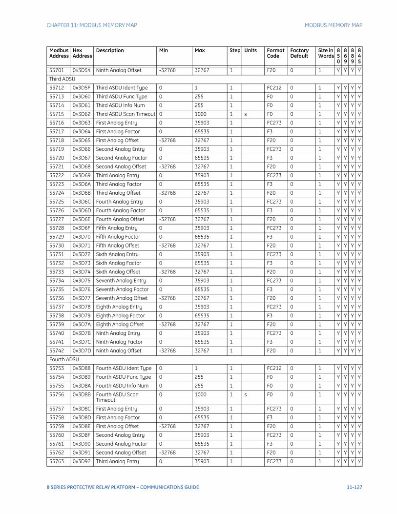
CHAPTER 11: MODBUS MEMORY MAP MODBUS MEMORY MAP
55701 0x3D54 Ninth Analog Offset -32768 32767 1 F20 0 1 Y Y Y Y
Third ADSU
55712 0x3D5F Third ASDU Ident Type 0 1 1 FC212 0 1 Y Y Y Y
55713 0x3D60 Third ASDU Func Type 0 255 1 F0 0 1 Y Y Y Y
55714 0x3D61 Third ASDU Info Num 0 255 1 F0 0 1 Y Y Y Y
55715 0x3D62 Third ASDU Scan Timeout 0 1000 1 s F0 0 1 Y Y Y Y
55716 0x3D63 First Analog Entry 0 35903 1 FC273 0 1 Y Y Y Y
55717 0x3D64 First Analog Factor 0 65535 1 F3 0 1 Y Y Y Y
55718 0x3D65 First Analog Offset -32768 32767 1 F20 0 1 Y Y Y Y
55719 0x3D66 Second Analog Entry 0 35903 1 FC273 0 1 Y Y Y Y
55720 0x3D67 Second Analog Factor 0 65535 1 F3 0 1 Y Y Y Y
55721 0x3D68 Second Analog Offset -32768 32767 1 F20 0 1 Y Y Y Y
55722 0x3D69 Third Analog Entry 0 35903 1 FC273 0 1 Y Y Y Y
55723 0x3D6A Third Analog Factor 0 65535 1 F3 0 1 Y Y Y Y
55724 0x3D6B Third Analog Offset -32768 32767 1 F20 0 1 Y Y Y Y
55725 0x3D6C Fourth Analog Entry 0 35903 1 FC273 0 1 Y Y Y Y
55726 0x3D6D Fourth Analog Factor 0 65535 1 F3 0 1 Y Y Y Y
55727 0x3D6E Fourth Analog Offset -32768 32767 1 F20 0 1 Y Y Y Y
55728 0x3D6F Fifth Analog Entry 0 35903 1 FC273 0 1 Y Y Y Y
55729 0x3D70 Fifth Analog Factor 0 65535 1 F3 0 1 Y Y Y Y
55730 0x3D71 Fifth Analog Offset -32768 32767 1 F20 0 1 Y Y Y Y
55731 0x3D72 Sixth Analog Entry 0 35903 1 FC273 0 1 Y Y Y Y
55732 0x3D73 Sixth Analog Factor 0 65535 1 F3 0 1 Y Y Y Y
55733 0x3D74 Sixth Analog Offset -32768 32767 1 F20 0 1 Y Y Y Y
55734 0x3D75 Seventh Analog Entry 0 35903 1 FC273 0 1 Y Y Y Y
55735 0x3D76 Seventh Analog Factor 0 65535 1 F3 0 1 Y Y Y Y
55736 0x3D77 Seventh Analog Offset -32768 32767 1 F20 0 1 Y Y Y Y
55737 0x3D78 Eighth Analog Entry 0 35903 1 FC273 0 1 Y Y Y Y
55738 0x3D79 Eighth Analog Factor 0 65535 1 F3 0 1 Y Y Y Y
55739 0x3D7A Eighth Analog Offset -32768 32767 1 F20 0 1 Y Y Y Y
55740 0x3D7B Ninth Analog Entry 0 35903 1 FC273 0 1 Y Y Y Y
55741 0x3D7C Ninth Analog Factor 0 65535 1 F3 0 1 Y Y Y Y
55742 0x3D7D Ninth Analog Offset -32768 32767 1 F20 0 1 Y Y Y Y
Fourth ADSU
55753 0x3D88 Fourth ASDU Ident Type 0 1 1 FC212 0 1 Y Y Y Y
55754 0x3D89 Fourth ASDU Func Type 0 255 1 F0 0 1 Y Y Y Y
55755 0x3D8A Fourth ASDU Info Num 0 255 1 F0 0 1 Y Y Y Y
55756 0x3D8B Fourth ASDU Scan Timeout
0 1000 1 s F0 0 1 Y Y Y Y
55757 0x3D8C First Analog Entry 0 35903 1 FC273 0 1 Y Y Y Y
55758 0x3D8D First Analog Factor 0 65535 1 F3 0 1 Y Y Y Y
55759 0x3D8E First Analog Offset -32768 32767 1 F20 0 1 Y Y Y Y
55760 0x3D8F Second Analog Entry 0 35903 1 FC273 0 1 Y Y Y Y
55761 0x3D90 Second Analog Factor 0 65535 1 F3 0 1 Y Y Y Y
55762 0x3D91 Second Analog Offset -32768 32767 1 F20 0 1 Y Y Y Y
55763 0x3D92 Third Analog Entry 0 35903 1 FC273 0 1 Y Y Y Y
Modbus Address
Hex Address
Description Min Max Step Units Format Code
Factory Default
Size in Words
850
869
889
845
8 SERIES PROTECTIVE RELAY PLATFORM – COMMUNICATIONS GUIDE 11-127
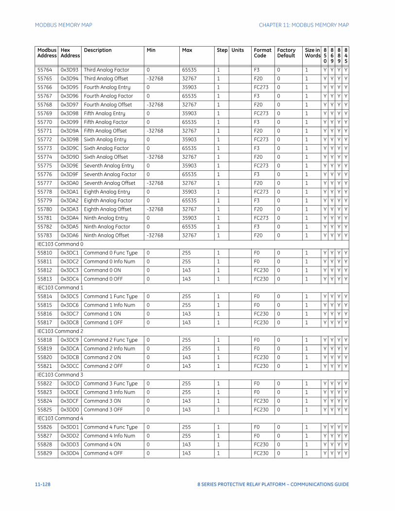
MODBUS MEMORY MAP CHAPTER 11: MODBUS MEMORY MAP
55764 0x3D93 Third Analog Factor 0 65535 1 F3 0 1 Y Y Y Y
55765 0x3D94 Third Analog Offset -32768 32767 1 F20 0 1 Y Y Y Y
55766 0x3D95 Fourth Analog Entry 0 35903 1 FC273 0 1 Y Y Y Y
55767 0x3D96 Fourth Analog Factor 0 65535 1 F3 0 1 Y Y Y Y
55768 0x3D97 Fourth Analog Offset -32768 32767 1 F20 0 1 Y Y Y Y
55769 0x3D98 Fifth Analog Entry 0 35903 1 FC273 0 1 Y Y Y Y
55770 0x3D99 Fifth Analog Factor 0 65535 1 F3 0 1 Y Y Y Y
55771 0x3D9A Fifth Analog Offset -32768 32767 1 F20 0 1 Y Y Y Y
55772 0x3D9B Sixth Analog Entry 0 35903 1 FC273 0 1 Y Y Y Y
55773 0x3D9C Sixth Analog Factor 0 65535 1 F3 0 1 Y Y Y Y
55774 0x3D9D Sixth Analog Offset -32768 32767 1 F20 0 1 Y Y Y Y
55775 0x3D9E Seventh Analog Entry 0 35903 1 FC273 0 1 Y Y Y Y
55776 0x3D9F Seventh Analog Factor 0 65535 1 F3 0 1 Y Y Y Y
55777 0x3DA0 Seventh Analog Offset -32768 32767 1 F20 0 1 Y Y Y Y
55778 0x3DA1 Eighth Analog Entry 0 35903 1 FC273 0 1 Y Y Y Y
55779 0x3DA2 Eighth Analog Factor 0 65535 1 F3 0 1 Y Y Y Y
55780 0x3DA3 Eighth Analog Offset -32768 32767 1 F20 0 1 Y Y Y Y
55781 0x3DA4 Ninth Analog Entry 0 35903 1 FC273 0 1 Y Y Y Y
55782 0x3DA5 Ninth Analog Factor 0 65535 1 F3 0 1 Y Y Y Y
55783 0x3DA6 Ninth Analog Offset -32768 32767 1 F20 0 1 Y Y Y Y
IEC103 Command 0
55810 0x3DC1 Command 0 Func Type 0 255 1 F0 0 1 Y Y Y Y
55811 0x3DC2 Command 0 Info Num 0 255 1 F0 0 1 Y Y Y Y
55812 0x3DC3 Command 0 ON 0 143 1 FC230 0 1 Y Y Y Y
55813 0x3DC4 Command 0 OFF 0 143 1 FC230 0 1 Y Y Y Y
IEC103 Command 1
55814 0x3DC5 Command 1 Func Type 0 255 1 F0 0 1 Y Y Y Y
55815 0x3DC6 Command 1 Info Num 0 255 1 F0 0 1 Y Y Y Y
55816 0x3DC7 Command 1 ON 0 143 1 FC230 0 1 Y Y Y Y
55817 0x3DC8 Command 1 OFF 0 143 1 FC230 0 1 Y Y Y Y
IEC103 Command 2
55818 0x3DC9 Command 2 Func Type 0 255 1 F0 0 1 Y Y Y Y
55819 0x3DCA Command 2 Info Num 0 255 1 F0 0 1 Y Y Y Y
55820 0x3DCB Command 2 ON 0 143 1 FC230 0 1 Y Y Y Y
55821 0x3DCC Command 2 OFF 0 143 1 FC230 0 1 Y Y Y Y
IEC103 Command 3
55822 0x3DCD Command 3 Func Type 0 255 1 F0 0 1 Y Y Y Y
55823 0x3DCE Command 3 Info Num 0 255 1 F0 0 1 Y Y Y Y
55824 0x3DCF Command 3 ON 0 143 1 FC230 0 1 Y Y Y Y
55825 0x3DD0 Command 3 OFF 0 143 1 FC230 0 1 Y Y Y Y
IEC103 Command 4
55826 0x3DD1 Command 4 Func Type 0 255 1 F0 0 1 Y Y Y Y
55827 0x3DD2 Command 4 Info Num 0 255 1 F0 0 1 Y Y Y Y
55828 0x3DD3 Command 4 ON 0 143 1 FC230 0 1 Y Y Y Y
55829 0x3DD4 Command 4 OFF 0 143 1 FC230 0 1 Y Y Y Y
Modbus Address
Hex Address
Description Min Max Step Units Format Code
Factory Default
Size in Words
850
869
889
845
11-128 8 SERIES PROTECTIVE RELAY PLATFORM – COMMUNICATIONS GUIDE
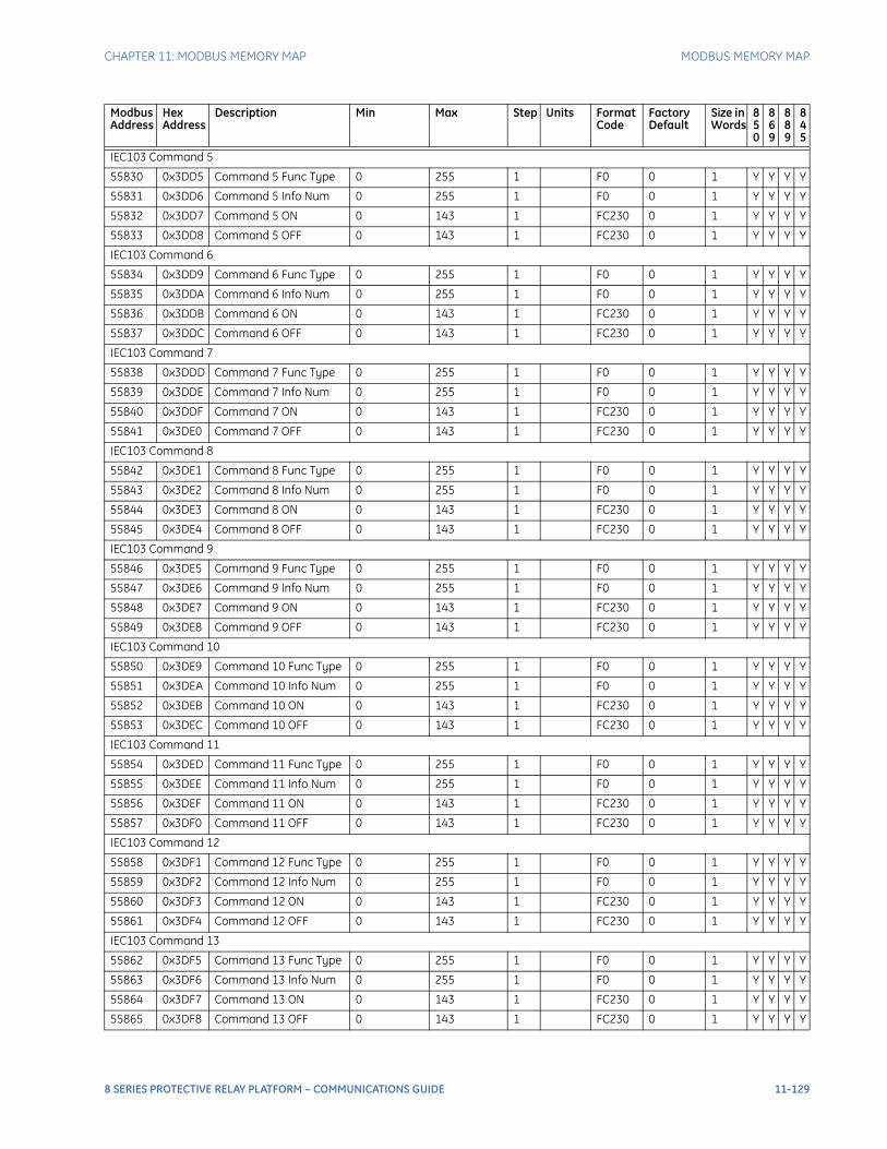
CHAPTER 11: MODBUS MEMORY MAP MODBUS MEMORY MAP
IEC103 Command 5
55830 0x3DD5 Command 5 Func Type 0 255 1 F0 0 1 Y Y Y Y
55831 0x3DD6 Command 5 Info Num 0 255 1 F0 0 1 Y Y Y Y
55832 0x3DD7 Command 5 ON 0 143 1 FC230 0 1 Y Y Y Y
55833 0x3DD8 Command 5 OFF 0 143 1 FC230 0 1 Y Y Y Y
IEC103 Command 6
55834 0x3DD9 Command 6 Func Type 0 255 1 F0 0 1 Y Y Y Y
55835 0x3DDA Command 6 Info Num 0 255 1 F0 0 1 Y Y Y Y
55836 0x3DDB Command 6 ON 0 143 1 FC230 0 1 Y Y Y Y
55837 0x3DDC Command 6 OFF 0 143 1 FC230 0 1 Y Y Y Y
IEC103 Command 7
55838 0x3DDD Command 7 Func Type 0 255 1 F0 0 1 Y Y Y Y
55839 0x3DDE Command 7 Info Num 0 255 1 F0 0 1 Y Y Y Y
55840 0x3DDF Command 7 ON 0 143 1 FC230 0 1 Y Y Y Y
55841 0x3DE0 Command 7 OFF 0 143 1 FC230 0 1 Y Y Y Y
IEC103 Command 8
55842 0x3DE1 Command 8 Func Type 0 255 1 F0 0 1 Y Y Y Y
55843 0x3DE2 Command 8 Info Num 0 255 1 F0 0 1 Y Y Y Y
55844 0x3DE3 Command 8 ON 0 143 1 FC230 0 1 Y Y Y Y
55845 0x3DE4 Command 8 OFF 0 143 1 FC230 0 1 Y Y Y Y
IEC103 Command 9
55846 0x3DE5 Command 9 Func Type 0 255 1 F0 0 1 Y Y Y Y
55847 0x3DE6 Command 9 Info Num 0 255 1 F0 0 1 Y Y Y Y
55848 0x3DE7 Command 9 ON 0 143 1 FC230 0 1 Y Y Y Y
55849 0x3DE8 Command 9 OFF 0 143 1 FC230 0 1 Y Y Y Y
IEC103 Command 10
55850 0x3DE9 Command 10 Func Type 0 255 1 F0 0 1 Y Y Y Y
55851 0x3DEA Command 10 Info Num 0 255 1 F0 0 1 Y Y Y Y
55852 0x3DEB Command 10 ON 0 143 1 FC230 0 1 Y Y Y Y
55853 0x3DEC Command 10 OFF 0 143 1 FC230 0 1 Y Y Y Y
IEC103 Command 11
55854 0x3DED Command 11 Func Type 0 255 1 F0 0 1 Y Y Y Y
55855 0x3DEE Command 11 Info Num 0 255 1 F0 0 1 Y Y Y Y
55856 0x3DEF Command 11 ON 0 143 1 FC230 0 1 Y Y Y Y
55857 0x3DF0 Command 11 OFF 0 143 1 FC230 0 1 Y Y Y Y
IEC103 Command 12
55858 0x3DF1 Command 12 Func Type 0 255 1 F0 0 1 Y Y Y Y
55859 0x3DF2 Command 12 Info Num 0 255 1 F0 0 1 Y Y Y Y
55860 0x3DF3 Command 12 ON 0 143 1 FC230 0 1 Y Y Y Y
55861 0x3DF4 Command 12 OFF 0 143 1 FC230 0 1 Y Y Y Y
IEC103 Command 13
55862 0x3DF5 Command 13 Func Type 0 255 1 F0 0 1 Y Y Y Y
55863 0x3DF6 Command 13 Info Num 0 255 1 F0 0 1 Y Y Y Y
55864 0x3DF7 Command 13 ON 0 143 1 FC230 0 1 Y Y Y Y
55865 0x3DF8 Command 13 OFF 0 143 1 FC230 0 1 Y Y Y Y
Modbus Address
Hex Address
Description Min Max Step Units Format Code
Factory Default
Size in Words
850
869
889
845
8 SERIES PROTECTIVE RELAY PLATFORM – COMMUNICATIONS GUIDE 11-129
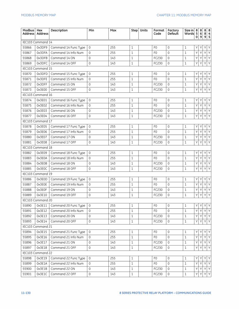
MODBUS MEMORY MAP CHAPTER 11: MODBUS MEMORY MAP
IEC103 Command 14
55866 0x3DF9 Command 14 Func Type 0 255 1 F0 0 1 Y Y Y Y
55867 0x3DFA Command 14 Info Num 0 255 1 F0 0 1 Y Y Y Y
55868 0x3DFB Command 14 ON 0 143 1 FC230 0 1 Y Y Y Y
55869 0x3DFC Command 14 OFF 0 143 1 FC230 0 1 Y Y Y Y
IEC103 Command 15
55870 0x3DFD Command 15 Func Type 0 255 1 F0 0 1 Y Y Y Y
55871 0x3DFE Command 15 Info Num 0 255 1 F0 0 1 Y Y Y Y
55872 0x3DFF Command 15 ON 0 143 1 FC230 0 1 Y Y Y Y
55873 0x3E00 Command 15 OFF 0 143 1 FC230 0 1 Y Y Y Y
IEC103 Command 16
55874 0x3E01 Command 16 Func Type 0 255 1 F0 0 1 Y Y Y Y
55875 0x3E02 Command 16 Info Num 0 255 1 F0 0 1 Y Y Y Y
55876 0x3E03 Command 16 ON 0 143 1 FC230 0 1 Y Y Y Y
55877 0x3E04 Command 16 OFF 0 143 1 FC230 0 1 Y Y Y Y
IEC103 Command 17
55878 0x3E05 Command 17 Func Type 0 255 1 F0 0 1 Y Y Y Y
55879 0x3E06 Command 17 Info Num 0 255 1 F0 0 1 Y Y Y Y
55880 0x3E07 Command 17 ON 0 143 1 FC230 0 1 Y Y Y Y
55881 0x3E08 Command 17 OFF 0 143 1 FC230 0 1 Y Y Y Y
IEC103 Command 18
55882 0x3E09 Command 18 Func Type 0 255 1 F0 0 1 Y Y Y Y
55883 0x3E0A Command 18 Info Num 0 255 1 F0 0 1 Y Y Y Y
55884 0x3E0B Command 18 ON 0 143 1 FC230 0 1 Y Y Y Y
55885 0x3E0C Command 18 OFF 0 143 1 FC230 0 1 Y Y Y Y
IEC103 Command 19
55886 0x3E0D Command 19 Func Type 0 255 1 F0 0 1 Y Y Y Y
55887 0x3E0E Command 19 Info Num 0 255 1 F0 0 1 Y Y Y Y
55888 0x3E0F Command 19 ON 0 143 1 FC230 0 1 Y Y Y Y
55889 0x3E10 Command 19 OFF 0 143 1 FC230 0 1 Y Y Y Y
IEC103 Command 20
55890 0x3E11 Command 20 Func Type 0 255 1 F0 0 1 Y Y Y Y
55891 0x3E12 Command 20 Info Num 0 255 1 F0 0 1 Y Y Y Y
55892 0x3E13 Command 20 ON 0 143 1 FC230 0 1 Y Y Y Y
55893 0x3E14 Command 20 OFF 0 143 1 FC230 0 1 Y Y Y Y
IEC103 Command 21
55894 0x3E15 Command 21 Func Type 0 255 1 F0 0 1 Y Y Y Y
55895 0x3E16 Command 21 Info Num 0 255 1 F0 0 1 Y Y Y Y
55896 0x3E17 Command 21 ON 0 143 1 FC230 0 1 Y Y Y Y
55897 0x3E18 Command 21 OFF 0 143 1 FC230 0 1 Y Y Y Y
IEC103 Command 22
55898 0x3E19 Command 22 Func Type 0 255 1 F0 0 1 Y Y Y Y
55899 0x3E1A Command 22 Info Num 0 255 1 F0 0 1 Y Y Y Y
55900 0x3E1B Command 22 ON 0 143 1 FC230 0 1 Y Y Y Y
55901 0x3E1C Command 22 OFF 0 143 1 FC230 0 1 Y Y Y Y
Modbus Address
Hex Address
Description Min Max Step Units Format Code
Factory Default
Size in Words
850
869
889
845
11-130 8 SERIES PROTECTIVE RELAY PLATFORM – COMMUNICATIONS GUIDE
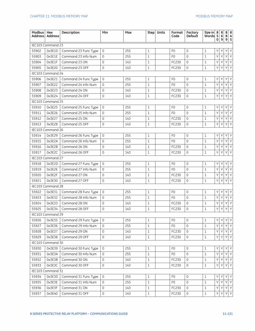
CHAPTER 11: MODBUS MEMORY MAP MODBUS MEMORY MAP
IEC103 Command 23
55902 0x3E1D Command 23 Func Type 0 255 1 F0 0 1 Y Y Y Y
55903 0x3E1E Command 23 Info Num 0 255 1 F0 0 1 Y Y Y Y
55904 0x3E1F Command 23 ON 0 143 1 FC230 0 1 Y Y Y Y
55905 0x3E20 Command 23 OFF 0 143 1 FC230 0 1 Y Y Y Y
IEC103 Command 24
55906 0x3E21 Command 24 Func Type 0 255 1 F0 0 1 Y Y Y Y
55907 0x3E22 Command 24 Info Num 0 255 1 F0 0 1 Y Y Y Y
55908 0x3E23 Command 24 ON 0 143 1 FC230 0 1 Y Y Y Y
55909 0x3E24 Command 24 OFF 0 143 1 FC230 0 1 Y Y Y Y
IEC103 Command 25
55910 0x3E25 Command 25 Func Type 0 255 1 F0 0 1 Y Y Y Y
55911 0x3E26 Command 25 Info Num 0 255 1 F0 0 1 Y Y Y Y
55912 0x3E27 Command 25 ON 0 143 1 FC230 0 1 Y Y Y Y
55913 0x3E28 Command 25 OFF 0 143 1 FC230 0 1 Y Y Y Y
IEC103 Command 26
55914 0x3E29 Command 26 Func Type 0 255 1 F0 0 1 Y Y Y Y
55915 0x3E2A Command 26 Info Num 0 255 1 F0 0 1 Y Y Y Y
55916 0x3E2B Command 26 ON 0 143 1 FC230 0 1 Y Y Y Y
55917 0x3E2C Command 26 OFF 0 143 1 FC230 0 1 Y Y Y Y
IEC103 Command 27
55918 0x3E2D Command 27 Func Type 0 255 1 F0 0 1 Y Y Y Y
55919 0x3E2E Command 27 Info Num 0 255 1 F0 0 1 Y Y Y Y
55920 0x3E2F Command 27 ON 0 143 1 FC230 0 1 Y Y Y Y
55921 0x3E30 Command 27 OFF 0 143 1 FC230 0 1 Y Y Y Y
IEC103 Command 28
55922 0x3E31 Command 28 Func Type 0 255 1 F0 0 1 Y Y Y Y
55923 0x3E32 Command 28 Info Num 0 255 1 F0 0 1 Y Y Y Y
55924 0x3E33 Command 28 ON 0 143 1 FC230 0 1 Y Y Y Y
55925 0x3E34 Command 28 OFF 0 143 1 FC230 0 1 Y Y Y Y
IEC103 Command 29
55926 0x3E35 Command 29 Func Type 0 255 1 F0 0 1 Y Y Y Y
55927 0x3E36 Command 29 Info Num 0 255 1 F0 0 1 Y Y Y Y
55928 0x3E37 Command 29 ON 0 143 1 FC230 0 1 Y Y Y Y
55929 0x3E38 Command 29 OFF 0 143 1 FC230 0 1 Y Y Y Y
IEC103 Command 30
55930 0x3E39 Command 30 Func Type 0 255 1 F0 0 1 Y Y Y Y
55931 0x3E3A Command 30 Info Num 0 255 1 F0 0 1 Y Y Y Y
55932 0x3E3B Command 30 ON 0 143 1 FC230 0 1 Y Y Y Y
55933 0x3E3C Command 30 OFF 0 143 1 FC230 0 1 Y Y Y Y
IEC103 Command 31
55934 0x3E3D Command 31 Func Type 0 255 1 F0 0 1 Y Y Y Y
55935 0x3E3E Command 31 Info Num 0 255 1 F0 0 1 Y Y Y Y
55936 0x3E3F Command 31 ON 0 143 1 FC230 0 1 Y Y Y Y
55937 0x3E40 Command 31 OFF 0 143 1 FC230 0 1 Y Y Y Y
Modbus Address
Hex Address
Description Min Max Step Units Format Code
Factory Default
Size in Words
850
869
889
845
8 SERIES PROTECTIVE RELAY PLATFORM – COMMUNICATIONS GUIDE 11-131
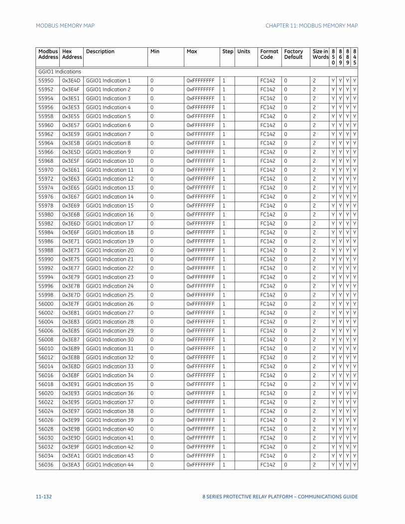
MODBUS MEMORY MAP CHAPTER 11: MODBUS MEMORY MAP
GGIO1 Indications
55950 0x3E4D GGIO1 Indication 1 0 0xFFFFFFFF 1 FC142 0 2 Y Y Y Y
55952 0x3E4F GGIO1 Indication 2 0 0xFFFFFFFF 1 FC142 0 2 Y Y Y Y
55954 0x3E51 GGIO1 Indication 3 0 0xFFFFFFFF 1 FC142 0 2 Y Y Y Y
55956 0x3E53 GGIO1 Indication 4 0 0xFFFFFFFF 1 FC142 0 2 Y Y Y Y
55958 0x3E55 GGIO1 Indication 5 0 0xFFFFFFFF 1 FC142 0 2 Y Y Y Y
55960 0x3E57 GGIO1 Indication 6 0 0xFFFFFFFF 1 FC142 0 2 Y Y Y Y
55962 0x3E59 GGIO1 Indication 7 0 0xFFFFFFFF 1 FC142 0 2 Y Y Y Y
55964 0x3E5B GGIO1 Indication 8 0 0xFFFFFFFF 1 FC142 0 2 Y Y Y Y
55966 0x3E5D GGIO1 Indication 9 0 0xFFFFFFFF 1 FC142 0 2 Y Y Y Y
55968 0x3E5F GGIO1 Indication 10 0 0xFFFFFFFF 1 FC142 0 2 Y Y Y Y
55970 0x3E61 GGIO1 Indication 11 0 0xFFFFFFFF 1 FC142 0 2 Y Y Y Y
55972 0x3E63 GGIO1 Indication 12 0 0xFFFFFFFF 1 FC142 0 2 Y Y Y Y
55974 0x3E65 GGIO1 Indication 13 0 0xFFFFFFFF 1 FC142 0 2 Y Y Y Y
55976 0x3E67 GGIO1 Indication 14 0 0xFFFFFFFF 1 FC142 0 2 Y Y Y Y
55978 0x3E69 GGIO1 Indication 15 0 0xFFFFFFFF 1 FC142 0 2 Y Y Y Y
55980 0x3E6B GGIO1 Indication 16 0 0xFFFFFFFF 1 FC142 0 2 Y Y Y Y
55982 0x3E6D GGIO1 Indication 17 0 0xFFFFFFFF 1 FC142 0 2 Y Y Y Y
55984 0x3E6F GGIO1 Indication 18 0 0xFFFFFFFF 1 FC142 0 2 Y Y Y Y
55986 0x3E71 GGIO1 Indication 19 0 0xFFFFFFFF 1 FC142 0 2 Y Y Y Y
55988 0x3E73 GGIO1 Indication 20 0 0xFFFFFFFF 1 FC142 0 2 Y Y Y Y
55990 0x3E75 GGIO1 Indication 21 0 0xFFFFFFFF 1 FC142 0 2 Y Y Y Y
55992 0x3E77 GGIO1 Indication 22 0 0xFFFFFFFF 1 FC142 0 2 Y Y Y Y
55994 0x3E79 GGIO1 Indication 23 0 0xFFFFFFFF 1 FC142 0 2 Y Y Y Y
55996 0x3E7B GGIO1 Indication 24 0 0xFFFFFFFF 1 FC142 0 2 Y Y Y Y
55998 0x3E7D GGIO1 Indication 25 0 0xFFFFFFFF 1 FC142 0 2 Y Y Y Y
56000 0x3E7F GGIO1 Indication 26 0 0xFFFFFFFF 1 FC142 0 2 Y Y Y Y
56002 0x3E81 GGIO1 Indication 27 0 0xFFFFFFFF 1 FC142 0 2 Y Y Y Y
56004 0x3E83 GGIO1 Indication 28 0 0xFFFFFFFF 1 FC142 0 2 Y Y Y Y
56006 0x3E85 GGIO1 Indication 29 0 0xFFFFFFFF 1 FC142 0 2 Y Y Y Y
56008 0x3E87 GGIO1 Indication 30 0 0xFFFFFFFF 1 FC142 0 2 Y Y Y Y
56010 0x3E89 GGIO1 Indication 31 0 0xFFFFFFFF 1 FC142 0 2 Y Y Y Y
56012 0x3E8B GGIO1 Indication 32 0 0xFFFFFFFF 1 FC142 0 2 Y Y Y Y
56014 0x3E8D GGIO1 Indication 33 0 0xFFFFFFFF 1 FC142 0 2 Y Y Y Y
56016 0x3E8F GGIO1 Indication 34 0 0xFFFFFFFF 1 FC142 0 2 Y Y Y Y
56018 0x3E91 GGIO1 Indication 35 0 0xFFFFFFFF 1 FC142 0 2 Y Y Y Y
56020 0x3E93 GGIO1 Indication 36 0 0xFFFFFFFF 1 FC142 0 2 Y Y Y Y
56022 0x3E95 GGIO1 Indication 37 0 0xFFFFFFFF 1 FC142 0 2 Y Y Y Y
56024 0x3E97 GGIO1 Indication 38 0 0xFFFFFFFF 1 FC142 0 2 Y Y Y Y
56026 0x3E99 GGIO1 Indication 39 0 0xFFFFFFFF 1 FC142 0 2 Y Y Y Y
56028 0x3E9B GGIO1 Indication 40 0 0xFFFFFFFF 1 FC142 0 2 Y Y Y Y
56030 0x3E9D GGIO1 Indication 41 0 0xFFFFFFFF 1 FC142 0 2 Y Y Y Y
56032 0x3E9F GGIO1 Indication 42 0 0xFFFFFFFF 1 FC142 0 2 Y Y Y Y
56034 0x3EA1 GGIO1 Indication 43 0 0xFFFFFFFF 1 FC142 0 2 Y Y Y Y
56036 0x3EA3 GGIO1 Indication 44 0 0xFFFFFFFF 1 FC142 0 2 Y Y Y Y
Modbus Address
Hex Address
Description Min Max Step Units Format Code
Factory Default
Size in Words
850
869
889
845
11-132 8 SERIES PROTECTIVE RELAY PLATFORM – COMMUNICATIONS GUIDE
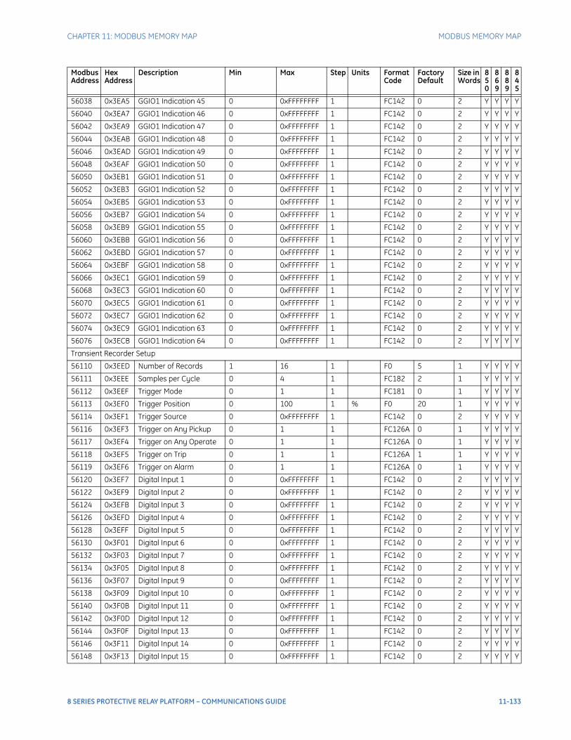
CHAPTER 11: MODBUS MEMORY MAP MODBUS MEMORY MAP
56038 0x3EA5 GGIO1 Indication 45 0 0xFFFFFFFF 1 FC142 0 2 Y Y Y Y
56040 0x3EA7 GGIO1 Indication 46 0 0xFFFFFFFF 1 FC142 0 2 Y Y Y Y
56042 0x3EA9 GGIO1 Indication 47 0 0xFFFFFFFF 1 FC142 0 2 Y Y Y Y
56044 0x3EAB GGIO1 Indication 48 0 0xFFFFFFFF 1 FC142 0 2 Y Y Y Y
56046 0x3EAD GGIO1 Indication 49 0 0xFFFFFFFF 1 FC142 0 2 Y Y Y Y
56048 0x3EAF GGIO1 Indication 50 0 0xFFFFFFFF 1 FC142 0 2 Y Y Y Y
56050 0x3EB1 GGIO1 Indication 51 0 0xFFFFFFFF 1 FC142 0 2 Y Y Y Y
56052 0x3EB3 GGIO1 Indication 52 0 0xFFFFFFFF 1 FC142 0 2 Y Y Y Y
56054 0x3EB5 GGIO1 Indication 53 0 0xFFFFFFFF 1 FC142 0 2 Y Y Y Y
56056 0x3EB7 GGIO1 Indication 54 0 0xFFFFFFFF 1 FC142 0 2 Y Y Y Y
56058 0x3EB9 GGIO1 Indication 55 0 0xFFFFFFFF 1 FC142 0 2 Y Y Y Y
56060 0x3EBB GGIO1 Indication 56 0 0xFFFFFFFF 1 FC142 0 2 Y Y Y Y
56062 0x3EBD GGIO1 Indication 57 0 0xFFFFFFFF 1 FC142 0 2 Y Y Y Y
56064 0x3EBF GGIO1 Indication 58 0 0xFFFFFFFF 1 FC142 0 2 Y Y Y Y
56066 0x3EC1 GGIO1 Indication 59 0 0xFFFFFFFF 1 FC142 0 2 Y Y Y Y
56068 0x3EC3 GGIO1 Indication 60 0 0xFFFFFFFF 1 FC142 0 2 Y Y Y Y
56070 0x3EC5 GGIO1 Indication 61 0 0xFFFFFFFF 1 FC142 0 2 Y Y Y Y
56072 0x3EC7 GGIO1 Indication 62 0 0xFFFFFFFF 1 FC142 0 2 Y Y Y Y
56074 0x3EC9 GGIO1 Indication 63 0 0xFFFFFFFF 1 FC142 0 2 Y Y Y Y
56076 0x3ECB GGIO1 Indication 64 0 0xFFFFFFFF 1 FC142 0 2 Y Y Y Y
Transient Recorder Setup
56110 0x3EED Number of Records 1 16 1 F0 5 1 Y Y Y Y
56111 0x3EEE Samples per Cycle 0 4 1 FC182 2 1 Y Y Y Y
56112 0x3EEF Trigger Mode 0 1 1 FC181 0 1 Y Y Y Y
56113 0x3EF0 Trigger Position 0 100 1 % F0 20 1 Y Y Y Y
56114 0x3EF1 Trigger Source 0 0xFFFFFFFF 1 FC142 0 2 Y Y Y Y
56116 0x3EF3 Trigger on Any Pickup 0 1 1 FC126A 0 1 Y Y Y Y
56117 0x3EF4 Trigger on Any Operate 0 1 1 FC126A 0 1 Y Y Y Y
56118 0x3EF5 Trigger on Trip 0 1 1 FC126A 1 1 Y Y Y Y
56119 0x3EF6 Trigger on Alarm 0 1 1 FC126A 0 1 Y Y Y Y
56120 0x3EF7 Digital Input 1 0 0xFFFFFFFF 1 FC142 0 2 Y Y Y Y
56122 0x3EF9 Digital Input 2 0 0xFFFFFFFF 1 FC142 0 2 Y Y Y Y
56124 0x3EFB Digital Input 3 0 0xFFFFFFFF 1 FC142 0 2 Y Y Y Y
56126 0x3EFD Digital Input 4 0 0xFFFFFFFF 1 FC142 0 2 Y Y Y Y
56128 0x3EFF Digital Input 5 0 0xFFFFFFFF 1 FC142 0 2 Y Y Y Y
56130 0x3F01 Digital Input 6 0 0xFFFFFFFF 1 FC142 0 2 Y Y Y Y
56132 0x3F03 Digital Input 7 0 0xFFFFFFFF 1 FC142 0 2 Y Y Y Y
56134 0x3F05 Digital Input 8 0 0xFFFFFFFF 1 FC142 0 2 Y Y Y Y
56136 0x3F07 Digital Input 9 0 0xFFFFFFFF 1 FC142 0 2 Y Y Y Y
56138 0x3F09 Digital Input 10 0 0xFFFFFFFF 1 FC142 0 2 Y Y Y Y
56140 0x3F0B Digital Input 11 0 0xFFFFFFFF 1 FC142 0 2 Y Y Y Y
56142 0x3F0D Digital Input 12 0 0xFFFFFFFF 1 FC142 0 2 Y Y Y Y
56144 0x3F0F Digital Input 13 0 0xFFFFFFFF 1 FC142 0 2 Y Y Y Y
56146 0x3F11 Digital Input 14 0 0xFFFFFFFF 1 FC142 0 2 Y Y Y Y
56148 0x3F13 Digital Input 15 0 0xFFFFFFFF 1 FC142 0 2 Y Y Y Y
Modbus Address
Hex Address
Description Min Max Step Units Format Code
Factory Default
Size in Words
850
869
889
845
8 SERIES PROTECTIVE RELAY PLATFORM – COMMUNICATIONS GUIDE 11-133

MODBUS MEMORY MAP CHAPTER 11: MODBUS MEMORY MAP
56150 0x3F15 Digital Input 16 0 0xFFFFFFFF 1 FC142 0 2 Y Y Y Y
56152 0x3F17 Digital Input 17 0 0xFFFFFFFF 1 FC142 0 2 Y Y Y Y
56154 0x3F19 Digital Input 18 0 0xFFFFFFFF 1 FC142 0 2 Y Y Y Y
56156 0x3F1B Digital Input 19 0 0xFFFFFFFF 1 FC142 0 2 Y Y Y Y
56158 0x3F1D Digital Input 20 0 0xFFFFFFFF 1 FC142 0 2 Y Y Y Y
56160 0x3F1F Digital Input 21 0 0xFFFFFFFF 1 FC142 0 2 Y Y Y Y
56162 0x3F21 Digital Input 22 0 0xFFFFFFFF 1 FC142 0 2 Y Y Y Y
56164 0x3F23 Digital Input 23 0 0xFFFFFFFF 1 FC142 0 2 Y Y Y Y
56166 0x3F25 Digital Input 24 0 0xFFFFFFFF 1 FC142 0 2 Y Y Y Y
56168 0x3F27 Digital Input 25 0 0xFFFFFFFF 1 FC142 0 2 Y Y Y Y
56170 0x3F29 Digital Input 26 0 0xFFFFFFFF 1 FC142 0 2 Y Y Y Y
56172 0x3F2B Digital Input 27 0 0xFFFFFFFF 1 FC142 0 2 Y Y Y Y
56174 0x3F2D Digital Input 28 0 0xFFFFFFFF 1 FC142 0 2 Y Y Y Y
56176 0x3F2F Digital Input 29 0 0xFFFFFFFF 1 FC142 0 2 Y Y Y Y
56178 0x3F31 Digital Input 30 0 0xFFFFFFFF 1 FC142 0 2 Y Y Y Y
56180 0x3F33 Digital Input 31 0 0xFFFFFFFF 1 FC142 0 2 Y Y Y Y
56182 0x3F35 Digital Input 32 0 0xFFFFFFFF 1 FC142 0 2 Y Y Y Y
56184 0x3F37 Analog Input 1 0 35903 1 FC273 0 1 Y Y Y Y
56185 0x3F38 Analog Input 2 0 35903 1 FC273 0 1 Y Y Y Y
56186 0x3F39 Analog Input 3 0 35903 1 FC273 0 1 Y Y Y Y
56187 0x3F3A Analog Input 4 0 35903 1 FC273 0 1 Y Y Y Y
56188 0x3F3B Analog Input 5 0 35903 1 FC273 0 1 Y Y Y Y
56189 0x3F3C Analog Input 6 0 35903 1 FC273 0 1 Y Y Y Y
56190 0x3F3D Analog Input 7 0 35903 1 FC273 0 1 Y Y Y Y
56191 0x3F3E Analog Input 8 0 35903 1 FC273 0 1 Y Y Y Y
56192 0x3F3F Analog Input 9 0 35903 1 FC273 0 1 Y Y Y Y
56193 0x3F40 Analog Input 10 0 35903 1 FC273 0 1 Y Y Y Y
56194 0x3F41 Analog Input 11 0 35903 1 FC273 0 1 Y Y Y Y
56195 0x3F42 Analog Input 12 0 35903 1 FC273 0 1 Y Y Y Y
56196 0x3F43 Analog Input 13 0 35903 1 FC273 0 1 Y Y Y Y
56197 0x3F44 Analog Input 14 0 35903 1 FC273 0 1 Y Y Y Y
56198 0x3F45 Analog Input 15 0 35903 1 FC273 0 1 Y Y Y Y
56199 0x3F46 Analog Input 16 0 35903 1 FC273 0 1 Y Y Y Y
Data Logger
56210 0x3F51 Function 0 2 1 FC186 0 1 Y Y Y Y
56211 0x3F52 Trigger 0 0xFFFFFFFF 1 FC142 0 2 Y Y Y Y
56213 0x3F54 Trigger Position 0 50 1 % F0 20 1 Y Y Y Y
56214 0x3F55 Rate 0 6 1 FC183 3 1 Y Y Y Y
56215 0x3F56 Channel 1 Source 0 35903 1 FC273 0 1 Y Y Y Y
56216 0x3F57 Channel 2 Source 0 35903 1 FC273 0 1 Y Y Y Y
56217 0x3F58 Channel 3 Source 0 35903 1 FC273 0 1 Y Y Y Y
56218 0x3F59 Channel 4 Source 0 35903 1 FC273 0 1 Y Y Y Y
56219 0x3F5A Channel 5 Source 0 35903 1 FC273 0 1 Y Y Y Y
56220 0x3F5B Channel 6 Source 0 35903 1 FC273 0 1 Y Y Y Y
56221 0x3F5C Channel 7 Source 0 35903 1 FC273 0 1 Y Y Y Y
Modbus Address
Hex Address
Description Min Max Step Units Format Code
Factory Default
Size in Words
850
869
889
845
11-134 8 SERIES PROTECTIVE RELAY PLATFORM – COMMUNICATIONS GUIDE
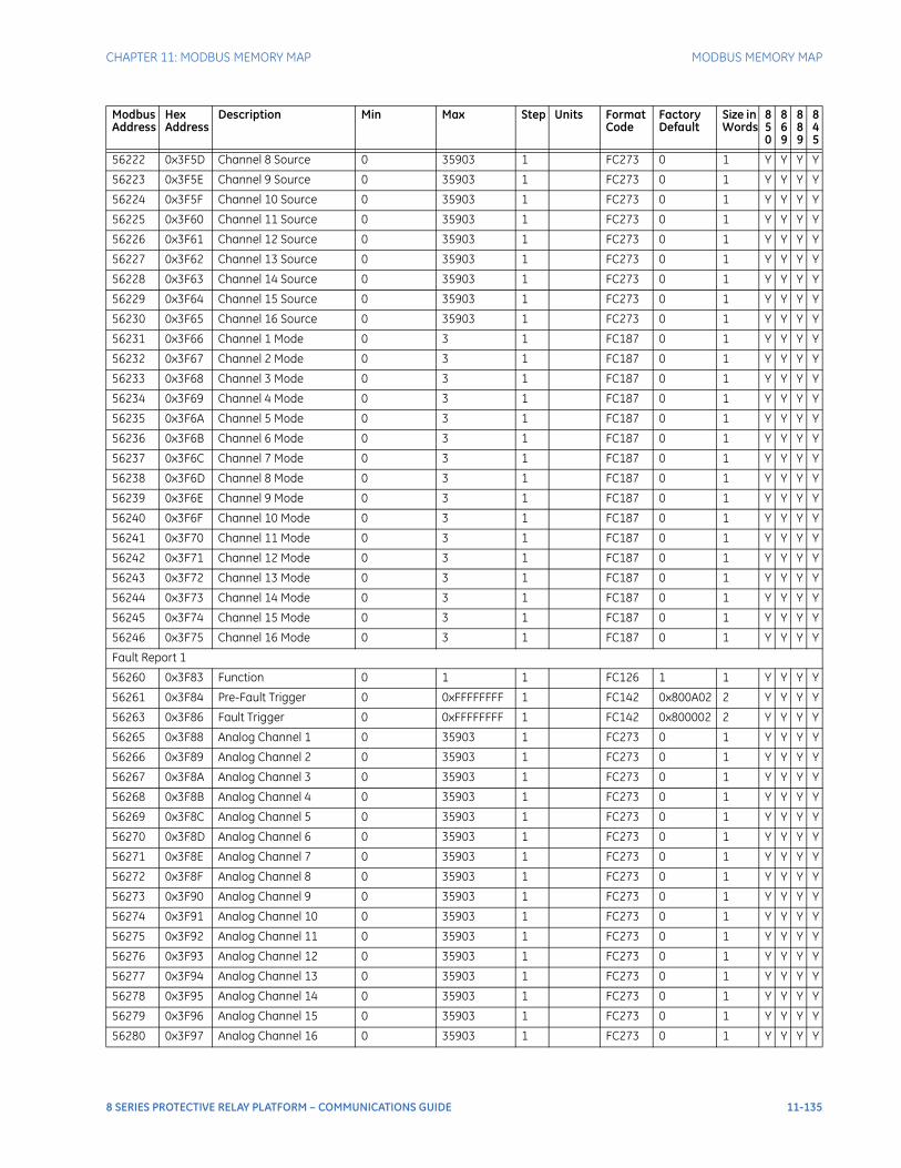
CHAPTER 11: MODBUS MEMORY MAP MODBUS MEMORY MAP
56222 0x3F5D Channel 8 Source 0 35903 1 FC273 0 1 Y Y Y Y
56223 0x3F5E Channel 9 Source 0 35903 1 FC273 0 1 Y Y Y Y
56224 0x3F5F Channel 10 Source 0 35903 1 FC273 0 1 Y Y Y Y
56225 0x3F60 Channel 11 Source 0 35903 1 FC273 0 1 Y Y Y Y
56226 0x3F61 Channel 12 Source 0 35903 1 FC273 0 1 Y Y Y Y
56227 0x3F62 Channel 13 Source 0 35903 1 FC273 0 1 Y Y Y Y
56228 0x3F63 Channel 14 Source 0 35903 1 FC273 0 1 Y Y Y Y
56229 0x3F64 Channel 15 Source 0 35903 1 FC273 0 1 Y Y Y Y
56230 0x3F65 Channel 16 Source 0 35903 1 FC273 0 1 Y Y Y Y
56231 0x3F66 Channel 1 Mode 0 3 1 FC187 0 1 Y Y Y Y
56232 0x3F67 Channel 2 Mode 0 3 1 FC187 0 1 Y Y Y Y
56233 0x3F68 Channel 3 Mode 0 3 1 FC187 0 1 Y Y Y Y
56234 0x3F69 Channel 4 Mode 0 3 1 FC187 0 1 Y Y Y Y
56235 0x3F6A Channel 5 Mode 0 3 1 FC187 0 1 Y Y Y Y
56236 0x3F6B Channel 6 Mode 0 3 1 FC187 0 1 Y Y Y Y
56237 0x3F6C Channel 7 Mode 0 3 1 FC187 0 1 Y Y Y Y
56238 0x3F6D Channel 8 Mode 0 3 1 FC187 0 1 Y Y Y Y
56239 0x3F6E Channel 9 Mode 0 3 1 FC187 0 1 Y Y Y Y
56240 0x3F6F Channel 10 Mode 0 3 1 FC187 0 1 Y Y Y Y
56241 0x3F70 Channel 11 Mode 0 3 1 FC187 0 1 Y Y Y Y
56242 0x3F71 Channel 12 Mode 0 3 1 FC187 0 1 Y Y Y Y
56243 0x3F72 Channel 13 Mode 0 3 1 FC187 0 1 Y Y Y Y
56244 0x3F73 Channel 14 Mode 0 3 1 FC187 0 1 Y Y Y Y
56245 0x3F74 Channel 15 Mode 0 3 1 FC187 0 1 Y Y Y Y
56246 0x3F75 Channel 16 Mode 0 3 1 FC187 0 1 Y Y Y Y
Fault Report 1
56260 0x3F83 Function 0 1 1 FC126 1 1 Y Y Y Y
56261 0x3F84 Pre-Fault Trigger 0 0xFFFFFFFF 1 FC142 0x800A02 2 Y Y Y Y
56263 0x3F86 Fault Trigger 0 0xFFFFFFFF 1 FC142 0x800002 2 Y Y Y Y
56265 0x3F88 Analog Channel 1 0 35903 1 FC273 0 1 Y Y Y Y
56266 0x3F89 Analog Channel 2 0 35903 1 FC273 0 1 Y Y Y Y
56267 0x3F8A Analog Channel 3 0 35903 1 FC273 0 1 Y Y Y Y
56268 0x3F8B Analog Channel 4 0 35903 1 FC273 0 1 Y Y Y Y
56269 0x3F8C Analog Channel 5 0 35903 1 FC273 0 1 Y Y Y Y
56270 0x3F8D Analog Channel 6 0 35903 1 FC273 0 1 Y Y Y Y
56271 0x3F8E Analog Channel 7 0 35903 1 FC273 0 1 Y Y Y Y
56272 0x3F8F Analog Channel 8 0 35903 1 FC273 0 1 Y Y Y Y
56273 0x3F90 Analog Channel 9 0 35903 1 FC273 0 1 Y Y Y Y
56274 0x3F91 Analog Channel 10 0 35903 1 FC273 0 1 Y Y Y Y
56275 0x3F92 Analog Channel 11 0 35903 1 FC273 0 1 Y Y Y Y
56276 0x3F93 Analog Channel 12 0 35903 1 FC273 0 1 Y Y Y Y
56277 0x3F94 Analog Channel 13 0 35903 1 FC273 0 1 Y Y Y Y
56278 0x3F95 Analog Channel 14 0 35903 1 FC273 0 1 Y Y Y Y
56279 0x3F96 Analog Channel 15 0 35903 1 FC273 0 1 Y Y Y Y
56280 0x3F97 Analog Channel 16 0 35903 1 FC273 0 1 Y Y Y Y
Modbus Address
Hex Address
Description Min Max Step Units Format Code
Factory Default
Size in Words
850
869
889
845
8 SERIES PROTECTIVE RELAY PLATFORM – COMMUNICATIONS GUIDE 11-135
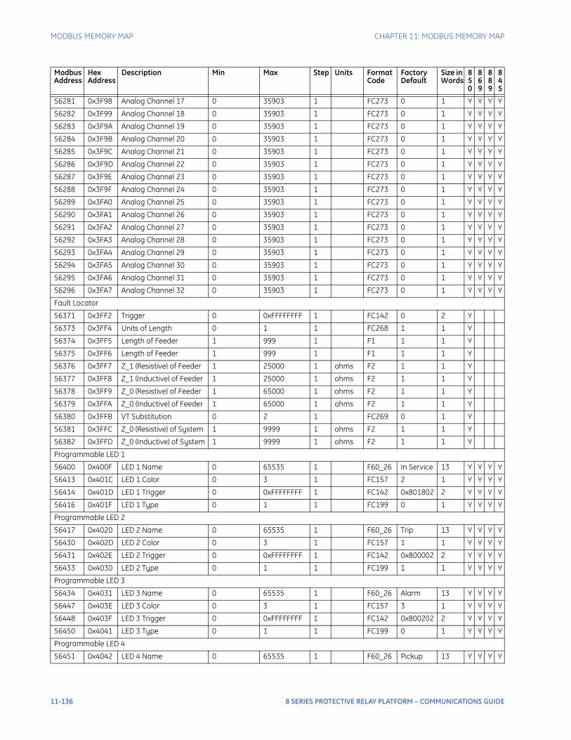
MODBUS MEMORY MAP CHAPTER 11: MODBUS MEMORY MAP
56281 0x3F98 Analog Channel 17 0 35903 1 FC273 0 1 Y Y Y Y
56282 0x3F99 Analog Channel 18 0 35903 1 FC273 0 1 Y Y Y Y
56283 0x3F9A Analog Channel 19 0 35903 1 FC273 0 1 Y Y Y Y
56284 0x3F9B Analog Channel 20 0 35903 1 FC273 0 1 Y Y Y Y
56285 0x3F9C Analog Channel 21 0 35903 1 FC273 0 1 Y Y Y Y
56286 0x3F9D Analog Channel 22 0 35903 1 FC273 0 1 Y Y Y Y
56287 0x3F9E Analog Channel 23 0 35903 1 FC273 0 1 Y Y Y Y
56288 0x3F9F Analog Channel 24 0 35903 1 FC273 0 1 Y Y Y Y
56289 0x3FA0 Analog Channel 25 0 35903 1 FC273 0 1 Y Y Y Y
56290 0x3FA1 Analog Channel 26 0 35903 1 FC273 0 1 Y Y Y Y
56291 0x3FA2 Analog Channel 27 0 35903 1 FC273 0 1 Y Y Y Y
56292 0x3FA3 Analog Channel 28 0 35903 1 FC273 0 1 Y Y Y Y
56293 0x3FA4 Analog Channel 29 0 35903 1 FC273 0 1 Y Y Y Y
56294 0x3FA5 Analog Channel 30 0 35903 1 FC273 0 1 Y Y Y Y
56295 0x3FA6 Analog Channel 31 0 35903 1 FC273 0 1 Y Y Y Y
56296 0x3FA7 Analog Channel 32 0 35903 1 FC273 0 1 Y Y Y Y
Fault Locator
56371 0x3FF2 Trigger 0 0xFFFFFFFF 1 FC142 0 2 Y
56373 0x3FF4 Units of Length 0 1 1 FC268 1 1 Y
56374 0x3FF5 Length of Feeder 1 999 1 F1 1 1 Y
56375 0x3FF6 Length of Feeder 1 999 1 F1 1 1 Y
56376 0x3FF7 Z_1 (Resistive) of Feeder 1 25000 1 ohms F2 1 1 Y
56377 0x3FF8 Z_1 (Inductive) of Feeder 1 25000 1 ohms F2 1 1 Y
56378 0x3FF9 Z_0 (Resistive) of Feeder 1 65000 1 ohms F2 1 1 Y
56379 0x3FFA Z_0 (Inductive) of Feeder 1 65000 1 ohms F2 1 1 Y
56380 0x3FFB VT Substitution 0 2 1 FC269 0 1 Y
56381 0x3FFC Z_0 (Resistive) of System 1 9999 1 ohms F2 1 1 Y
56382 0x3FFD Z_0 (Inductive) of System 1 9999 1 ohms F2 1 1 Y
Programmable LED 1
56400 0x400F LED 1 Name 0 65535 1 F60_26 In Service 13 Y Y Y Y
56413 0x401C LED 1 Color 0 3 1 FC157 2 1 Y Y Y Y
56414 0x401D LED 1 Trigger 0 0xFFFFFFFF 1 FC142 0x801802 2 Y Y Y Y
56416 0x401F LED 1 Type 0 1 1 FC199 0 1 Y Y Y Y
Programmable LED 2
56417 0x4020 LED 2 Name 0 65535 1 F60_26 Trip 13 Y Y Y Y
56430 0x402D LED 2 Color 0 3 1 FC157 1 1 Y Y Y Y
56431 0x402E LED 2 Trigger 0 0xFFFFFFFF 1 FC142 0x800002 2 Y Y Y Y
56433 0x4030 LED 2 Type 0 1 1 FC199 1 1 Y Y Y Y
Programmable LED 3
56434 0x4031 LED 3 Name 0 65535 1 F60_26 Alarm 13 Y Y Y Y
56447 0x403E LED 3 Color 0 3 1 FC157 3 1 Y Y Y Y
56448 0x403F LED 3 Trigger 0 0xFFFFFFFF 1 FC142 0x800202 2 Y Y Y Y
56450 0x4041 LED 3 Type 0 1 1 FC199 0 1 Y Y Y Y
Programmable LED 4
56451 0x4042 LED 4 Name 0 65535 1 F60_26 Pickup 13 Y Y Y Y
Modbus Address
Hex Address
Description Min Max Step Units Format Code
Factory Default
Size in Words
850
869
889
845
11-136 8 SERIES PROTECTIVE RELAY PLATFORM – COMMUNICATIONS GUIDE
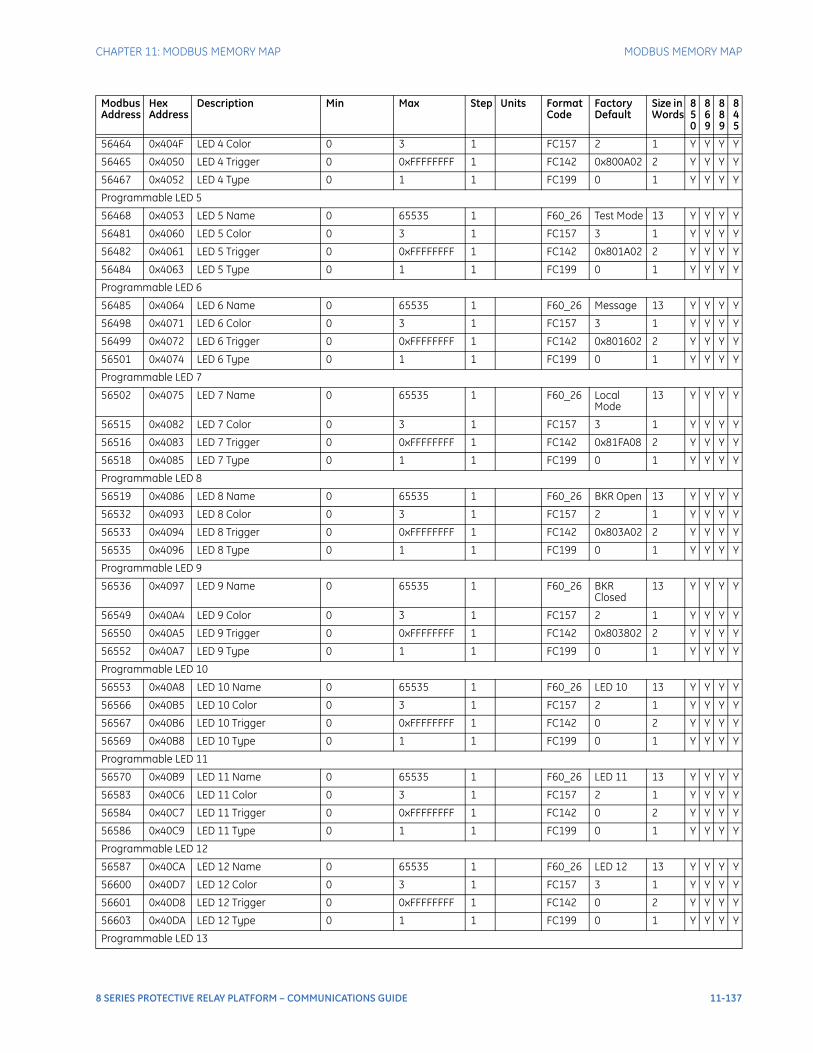
CHAPTER 11: MODBUS MEMORY MAP MODBUS MEMORY MAP
56464 0x404F LED 4 Color 0 3 1 FC157 2 1 Y Y Y Y
56465 0x4050 LED 4 Trigger 0 0xFFFFFFFF 1 FC142 0x800A02 2 Y Y Y Y
56467 0x4052 LED 4 Type 0 1 1 FC199 0 1 Y Y Y Y
Programmable LED 5
56468 0x4053 LED 5 Name 0 65535 1 F60_26 Test Mode 13 Y Y Y Y
56481 0x4060 LED 5 Color 0 3 1 FC157 3 1 Y Y Y Y
56482 0x4061 LED 5 Trigger 0 0xFFFFFFFF 1 FC142 0x801A02 2 Y Y Y Y
56484 0x4063 LED 5 Type 0 1 1 FC199 0 1 Y Y Y Y
Programmable LED 6
56485 0x4064 LED 6 Name 0 65535 1 F60_26 Message 13 Y Y Y Y
56498 0x4071 LED 6 Color 0 3 1 FC157 3 1 Y Y Y Y
56499 0x4072 LED 6 Trigger 0 0xFFFFFFFF 1 FC142 0x801602 2 Y Y Y Y
56501 0x4074 LED 6 Type 0 1 1 FC199 0 1 Y Y Y Y
Programmable LED 7
56502 0x4075 LED 7 Name 0 65535 1 F60_26 Local Mode
13 Y Y Y Y
56515 0x4082 LED 7 Color 0 3 1 FC157 3 1 Y Y Y Y
56516 0x4083 LED 7 Trigger 0 0xFFFFFFFF 1 FC142 0x81FA08 2 Y Y Y Y
56518 0x4085 LED 7 Type 0 1 1 FC199 0 1 Y Y Y Y
Programmable LED 8
56519 0x4086 LED 8 Name 0 65535 1 F60_26 BKR Open 13 Y Y Y Y
56532 0x4093 LED 8 Color 0 3 1 FC157 2 1 Y Y Y Y
56533 0x4094 LED 8 Trigger 0 0xFFFFFFFF 1 FC142 0x803A02 2 Y Y Y Y
56535 0x4096 LED 8 Type 0 1 1 FC199 0 1 Y Y Y Y
Programmable LED 9
56536 0x4097 LED 9 Name 0 65535 1 F60_26 BKR Closed
13 Y Y Y Y
56549 0x40A4 LED 9 Color 0 3 1 FC157 2 1 Y Y Y Y
56550 0x40A5 LED 9 Trigger 0 0xFFFFFFFF 1 FC142 0x803802 2 Y Y Y Y
56552 0x40A7 LED 9 Type 0 1 1 FC199 0 1 Y Y Y Y
Programmable LED 10
56553 0x40A8 LED 10 Name 0 65535 1 F60_26 LED 10 13 Y Y Y Y
56566 0x40B5 LED 10 Color 0 3 1 FC157 2 1 Y Y Y Y
56567 0x40B6 LED 10 Trigger 0 0xFFFFFFFF 1 FC142 0 2 Y Y Y Y
56569 0x40B8 LED 10 Type 0 1 1 FC199 0 1 Y Y Y Y
Programmable LED 11
56570 0x40B9 LED 11 Name 0 65535 1 F60_26 LED 11 13 Y Y Y Y
56583 0x40C6 LED 11 Color 0 3 1 FC157 2 1 Y Y Y Y
56584 0x40C7 LED 11 Trigger 0 0xFFFFFFFF 1 FC142 0 2 Y Y Y Y
56586 0x40C9 LED 11 Type 0 1 1 FC199 0 1 Y Y Y Y
Programmable LED 12
56587 0x40CA LED 12 Name 0 65535 1 F60_26 LED 12 13 Y Y Y Y
56600 0x40D7 LED 12 Color 0 3 1 FC157 3 1 Y Y Y Y
56601 0x40D8 LED 12 Trigger 0 0xFFFFFFFF 1 FC142 0 2 Y Y Y Y
56603 0x40DA LED 12 Type 0 1 1 FC199 0 1 Y Y Y Y
Programmable LED 13
Modbus Address
Hex Address
Description Min Max Step Units Format Code
Factory Default
Size in Words
850
869
889
845
8 SERIES PROTECTIVE RELAY PLATFORM – COMMUNICATIONS GUIDE 11-137
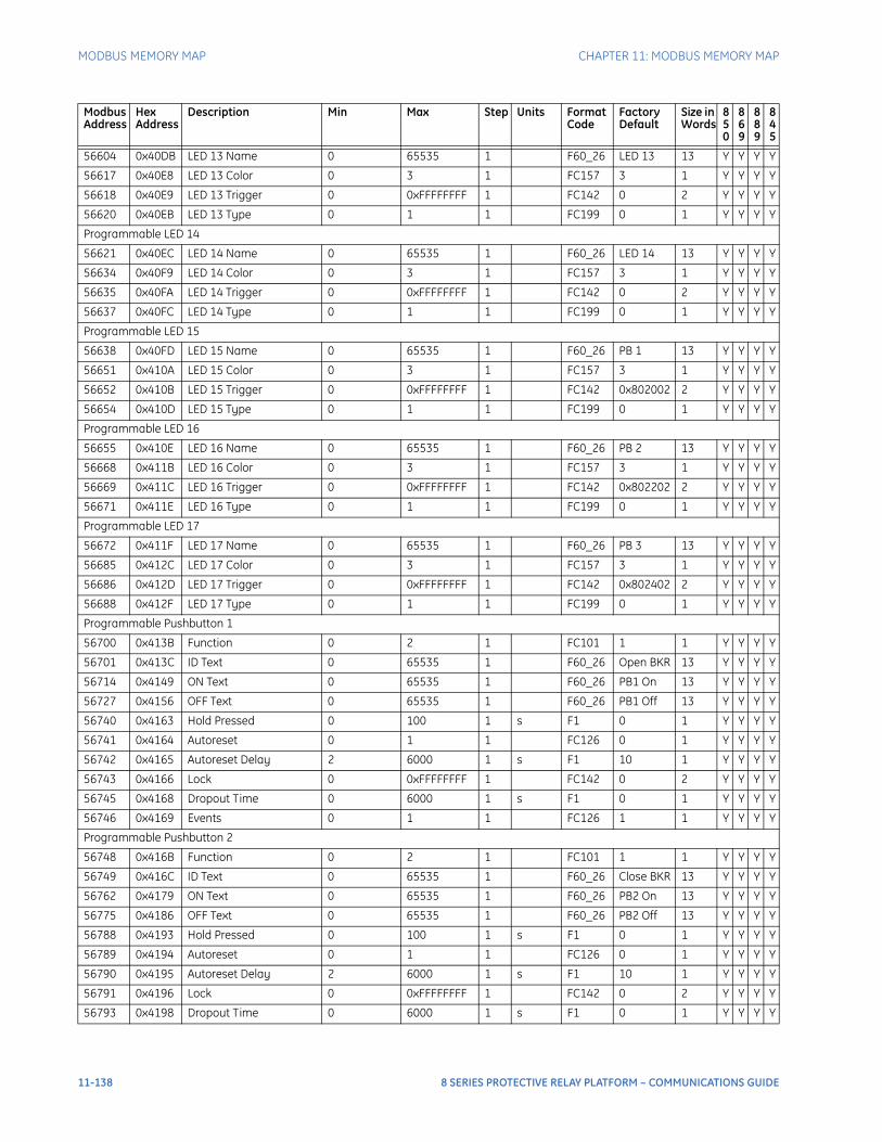
MODBUS MEMORY MAP CHAPTER 11: MODBUS MEMORY MAP
56604 0x40DB LED 13 Name 0 65535 1 F60_26 LED 13 13 Y Y Y Y
56617 0x40E8 LED 13 Color 0 3 1 FC157 3 1 Y Y Y Y
56618 0x40E9 LED 13 Trigger 0 0xFFFFFFFF 1 FC142 0 2 Y Y Y Y
56620 0x40EB LED 13 Type 0 1 1 FC199 0 1 Y Y Y Y
Programmable LED 14
56621 0x40EC LED 14 Name 0 65535 1 F60_26 LED 14 13 Y Y Y Y
56634 0x40F9 LED 14 Color 0 3 1 FC157 3 1 Y Y Y Y
56635 0x40FA LED 14 Trigger 0 0xFFFFFFFF 1 FC142 0 2 Y Y Y Y
56637 0x40FC LED 14 Type 0 1 1 FC199 0 1 Y Y Y Y
Programmable LED 15
56638 0x40FD LED 15 Name 0 65535 1 F60_26 PB 1 13 Y Y Y Y
56651 0x410A LED 15 Color 0 3 1 FC157 3 1 Y Y Y Y
56652 0x410B LED 15 Trigger 0 0xFFFFFFFF 1 FC142 0x802002 2 Y Y Y Y
56654 0x410D LED 15 Type 0 1 1 FC199 0 1 Y Y Y Y
Programmable LED 16
56655 0x410E LED 16 Name 0 65535 1 F60_26 PB 2 13 Y Y Y Y
56668 0x411B LED 16 Color 0 3 1 FC157 3 1 Y Y Y Y
56669 0x411C LED 16 Trigger 0 0xFFFFFFFF 1 FC142 0x802202 2 Y Y Y Y
56671 0x411E LED 16 Type 0 1 1 FC199 0 1 Y Y Y Y
Programmable LED 17
56672 0x411F LED 17 Name 0 65535 1 F60_26 PB 3 13 Y Y Y Y
56685 0x412C LED 17 Color 0 3 1 FC157 3 1 Y Y Y Y
56686 0x412D LED 17 Trigger 0 0xFFFFFFFF 1 FC142 0x802402 2 Y Y Y Y
56688 0x412F LED 17 Type 0 1 1 FC199 0 1 Y Y Y Y
Programmable Pushbutton 1
56700 0x413B Function 0 2 1 FC101 1 1 Y Y Y Y
56701 0x413C ID Text 0 65535 1 F60_26 Open BKR 13 Y Y Y Y
56714 0x4149 ON Text 0 65535 1 F60_26 PB1 On 13 Y Y Y Y
56727 0x4156 OFF Text 0 65535 1 F60_26 PB1 Off 13 Y Y Y Y
56740 0x4163 Hold Pressed 0 100 1 s F1 0 1 Y Y Y Y
56741 0x4164 Autoreset 0 1 1 FC126 0 1 Y Y Y Y
56742 0x4165 Autoreset Delay 2 6000 1 s F1 10 1 Y Y Y Y
56743 0x4166 Lock 0 0xFFFFFFFF 1 FC142 0 2 Y Y Y Y
56745 0x4168 Dropout Time 0 6000 1 s F1 0 1 Y Y Y Y
56746 0x4169 Events 0 1 1 FC126 1 1 Y Y Y Y
Programmable Pushbutton 2
56748 0x416B Function 0 2 1 FC101 1 1 Y Y Y Y
56749 0x416C ID Text 0 65535 1 F60_26 Close BKR 13 Y Y Y Y
56762 0x4179 ON Text 0 65535 1 F60_26 PB2 On 13 Y Y Y Y
56775 0x4186 OFF Text 0 65535 1 F60_26 PB2 Off 13 Y Y Y Y
56788 0x4193 Hold Pressed 0 100 1 s F1 0 1 Y Y Y Y
56789 0x4194 Autoreset 0 1 1 FC126 0 1 Y Y Y Y
56790 0x4195 Autoreset Delay 2 6000 1 s F1 10 1 Y Y Y Y
56791 0x4196 Lock 0 0xFFFFFFFF 1 FC142 0 2 Y Y Y Y
56793 0x4198 Dropout Time 0 6000 1 s F1 0 1 Y Y Y Y
Modbus Address
Hex Address
Description Min Max Step Units Format Code
Factory Default
Size in Words
850
869
889
845
11-138 8 SERIES PROTECTIVE RELAY PLATFORM – COMMUNICATIONS GUIDE
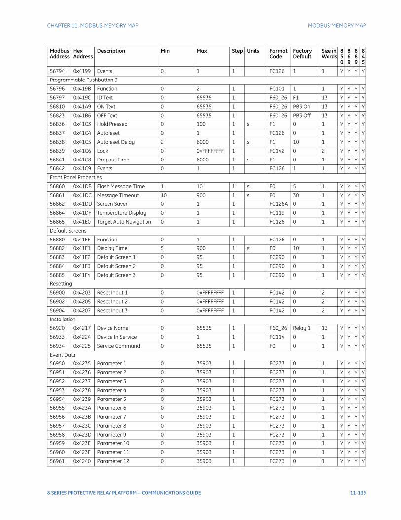
CHAPTER 11: MODBUS MEMORY MAP MODBUS MEMORY MAP
56794 0x4199 Events 0 1 1 FC126 1 1 Y Y Y Y
Programmable Pushbutton 3
56796 0x419B Function 0 2 1 FC101 1 1 Y Y Y Y
56797 0x419C ID Text 0 65535 1 F60_26 F1 13 Y Y Y Y
56810 0x41A9 ON Text 0 65535 1 F60_26 PB3 On 13 Y Y Y Y
56823 0x41B6 OFF Text 0 65535 1 F60_26 PB3 Off 13 Y Y Y Y
56836 0x41C3 Hold Pressed 0 100 1 s F1 0 1 Y Y Y Y
56837 0x41C4 Autoreset 0 1 1 FC126 0 1 Y Y Y Y
56838 0x41C5 Autoreset Delay 2 6000 1 s F1 10 1 Y Y Y Y
56839 0x41C6 Lock 0 0xFFFFFFFF 1 FC142 0 2 Y Y Y Y
56841 0x41C8 Dropout Time 0 6000 1 s F1 0 1 Y Y Y Y
56842 0x41C9 Events 0 1 1 FC126 1 1 Y Y Y Y
Front Panel Properties
56860 0x41DB Flash Message Time 1 10 1 s F0 5 1 Y Y Y Y
56861 0x41DC Message Timeout 10 900 1 s F0 30 1 Y Y Y Y
56862 0x41DD Screen Saver 0 1 1 FC126A 0 1 Y Y Y Y
56864 0x41DF Temperature Display 0 1 1 FC119 0 1 Y Y Y Y
56865 0x41E0 Target Auto Navigation 0 1 1 FC126 0 1 Y Y Y Y
Default Screens
56880 0x41EF Function 0 1 1 FC126 0 1 Y Y Y Y
56882 0x41F1 Display Time 5 900 1 s F0 10 1 Y Y Y Y
56883 0x41F2 Default Screen 1 0 95 1 FC290 0 1 Y Y Y Y
56884 0x41F3 Default Screen 2 0 95 1 FC290 0 1 Y Y Y Y
56885 0x41F4 Default Screen 3 0 95 1 FC290 0 1 Y Y Y Y
Resetting
56900 0x4203 Reset Input 1 0 0xFFFFFFFF 1 FC142 0 2 Y Y Y Y
56902 0x4205 Reset Input 2 0 0xFFFFFFFF 1 FC142 0 2 Y Y Y Y
56904 0x4207 Reset Input 3 0 0xFFFFFFFF 1 FC142 0 2 Y Y Y Y
Installation
56920 0x4217 Device Name 0 65535 1 F60_26 Relay 1 13 Y Y Y Y
56933 0x4224 Device In Service 0 1 1 FC114 0 1 Y Y Y Y
56934 0x4225 Service Command 0 65535 1 F0 0 1 Y Y Y Y
Event Data
56950 0x4235 Parameter 1 0 35903 1 FC273 0 1 Y Y Y Y
56951 0x4236 Parameter 2 0 35903 1 FC273 0 1 Y Y Y Y
56952 0x4237 Parameter 3 0 35903 1 FC273 0 1 Y Y Y Y
56953 0x4238 Parameter 4 0 35903 1 FC273 0 1 Y Y Y Y
56954 0x4239 Parameter 5 0 35903 1 FC273 0 1 Y Y Y Y
56955 0x423A Parameter 6 0 35903 1 FC273 0 1 Y Y Y Y
56956 0x423B Parameter 7 0 35903 1 FC273 0 1 Y Y Y Y
56957 0x423C Parameter 8 0 35903 1 FC273 0 1 Y Y Y Y
56958 0x423D Parameter 9 0 35903 1 FC273 0 1 Y Y Y Y
56959 0x423E Parameter 10 0 35903 1 FC273 0 1 Y Y Y Y
56960 0x423F Parameter 11 0 35903 1 FC273 0 1 Y Y Y Y
56961 0x4240 Parameter 12 0 35903 1 FC273 0 1 Y Y Y Y
Modbus Address
Hex Address
Description Min Max Step Units Format Code
Factory Default
Size in Words
850
869
889
845
8 SERIES PROTECTIVE RELAY PLATFORM – COMMUNICATIONS GUIDE 11-139
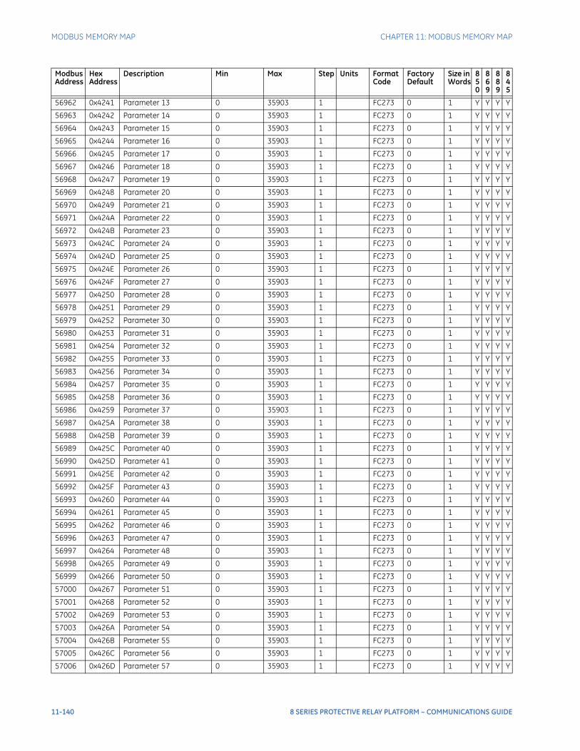
MODBUS MEMORY MAP CHAPTER 11: MODBUS MEMORY MAP
56962 0x4241 Parameter 13 0 35903 1 FC273 0 1 Y Y Y Y
56963 0x4242 Parameter 14 0 35903 1 FC273 0 1 Y Y Y Y
56964 0x4243 Parameter 15 0 35903 1 FC273 0 1 Y Y Y Y
56965 0x4244 Parameter 16 0 35903 1 FC273 0 1 Y Y Y Y
56966 0x4245 Parameter 17 0 35903 1 FC273 0 1 Y Y Y Y
56967 0x4246 Parameter 18 0 35903 1 FC273 0 1 Y Y Y Y
56968 0x4247 Parameter 19 0 35903 1 FC273 0 1 Y Y Y Y
56969 0x4248 Parameter 20 0 35903 1 FC273 0 1 Y Y Y Y
56970 0x4249 Parameter 21 0 35903 1 FC273 0 1 Y Y Y Y
56971 0x424A Parameter 22 0 35903 1 FC273 0 1 Y Y Y Y
56972 0x424B Parameter 23 0 35903 1 FC273 0 1 Y Y Y Y
56973 0x424C Parameter 24 0 35903 1 FC273 0 1 Y Y Y Y
56974 0x424D Parameter 25 0 35903 1 FC273 0 1 Y Y Y Y
56975 0x424E Parameter 26 0 35903 1 FC273 0 1 Y Y Y Y
56976 0x424F Parameter 27 0 35903 1 FC273 0 1 Y Y Y Y
56977 0x4250 Parameter 28 0 35903 1 FC273 0 1 Y Y Y Y
56978 0x4251 Parameter 29 0 35903 1 FC273 0 1 Y Y Y Y
56979 0x4252 Parameter 30 0 35903 1 FC273 0 1 Y Y Y Y
56980 0x4253 Parameter 31 0 35903 1 FC273 0 1 Y Y Y Y
56981 0x4254 Parameter 32 0 35903 1 FC273 0 1 Y Y Y Y
56982 0x4255 Parameter 33 0 35903 1 FC273 0 1 Y Y Y Y
56983 0x4256 Parameter 34 0 35903 1 FC273 0 1 Y Y Y Y
56984 0x4257 Parameter 35 0 35903 1 FC273 0 1 Y Y Y Y
56985 0x4258 Parameter 36 0 35903 1 FC273 0 1 Y Y Y Y
56986 0x4259 Parameter 37 0 35903 1 FC273 0 1 Y Y Y Y
56987 0x425A Parameter 38 0 35903 1 FC273 0 1 Y Y Y Y
56988 0x425B Parameter 39 0 35903 1 FC273 0 1 Y Y Y Y
56989 0x425C Parameter 40 0 35903 1 FC273 0 1 Y Y Y Y
56990 0x425D Parameter 41 0 35903 1 FC273 0 1 Y Y Y Y
56991 0x425E Parameter 42 0 35903 1 FC273 0 1 Y Y Y Y
56992 0x425F Parameter 43 0 35903 1 FC273 0 1 Y Y Y Y
56993 0x4260 Parameter 44 0 35903 1 FC273 0 1 Y Y Y Y
56994 0x4261 Parameter 45 0 35903 1 FC273 0 1 Y Y Y Y
56995 0x4262 Parameter 46 0 35903 1 FC273 0 1 Y Y Y Y
56996 0x4263 Parameter 47 0 35903 1 FC273 0 1 Y Y Y Y
56997 0x4264 Parameter 48 0 35903 1 FC273 0 1 Y Y Y Y
56998 0x4265 Parameter 49 0 35903 1 FC273 0 1 Y Y Y Y
56999 0x4266 Parameter 50 0 35903 1 FC273 0 1 Y Y Y Y
57000 0x4267 Parameter 51 0 35903 1 FC273 0 1 Y Y Y Y
57001 0x4268 Parameter 52 0 35903 1 FC273 0 1 Y Y Y Y
57002 0x4269 Parameter 53 0 35903 1 FC273 0 1 Y Y Y Y
57003 0x426A Parameter 54 0 35903 1 FC273 0 1 Y Y Y Y
57004 0x426B Parameter 55 0 35903 1 FC273 0 1 Y Y Y Y
57005 0x426C Parameter 56 0 35903 1 FC273 0 1 Y Y Y Y
57006 0x426D Parameter 57 0 35903 1 FC273 0 1 Y Y Y Y
Modbus Address
Hex Address
Description Min Max Step Units Format Code
Factory Default
Size in Words
850
869
889
845
11-140 8 SERIES PROTECTIVE RELAY PLATFORM – COMMUNICATIONS GUIDE
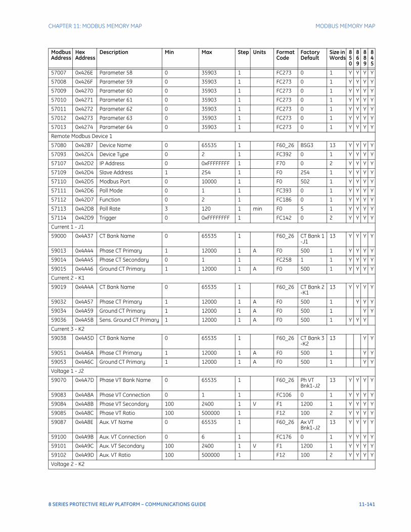
CHAPTER 11: MODBUS MEMORY MAP MODBUS MEMORY MAP
57007 0x426E Parameter 58 0 35903 1 FC273 0 1 Y Y Y Y
57008 0x426F Parameter 59 0 35903 1 FC273 0 1 Y Y Y Y
57009 0x4270 Parameter 60 0 35903 1 FC273 0 1 Y Y Y Y
57010 0x4271 Parameter 61 0 35903 1 FC273 0 1 Y Y Y Y
57011 0x4272 Parameter 62 0 35903 1 FC273 0 1 Y Y Y Y
57012 0x4273 Parameter 63 0 35903 1 FC273 0 1 Y Y Y Y
57013 0x4274 Parameter 64 0 35903 1 FC273 0 1 Y Y Y Y
Remote Modbus Device 1
57080 0x42B7 Device Name 0 65535 1 F60_26 BSG3 13 Y Y Y Y
57093 0x42C4 Device Type 0 2 1 FC392 0 1 Y Y Y Y
57107 0x42D2 IP Address 0 0xFFFFFFFF 1 F70 0 2 Y Y Y Y
57109 0x42D4 Slave Address 1 254 1 F0 254 1 Y Y Y Y
57110 0x42D5 Modbus Port 0 10000 1 F0 502 1 Y Y Y Y
57111 0x42D6 Poll Mode 0 1 1 FC393 0 1 Y Y Y Y
57112 0x42D7 Function 0 2 1 FC186 0 1 Y Y Y Y
57113 0x42D8 Poll Rate 3 120 1 min F0 5 1 Y Y Y Y
57114 0x42D9 Trigger 0 0xFFFFFFFF 1 FC142 0 2 Y Y Y Y
Current 1 - J1
59000 0x4A37 CT Bank Name 0 65535 1 F60_26 CT Bank 1 -J1
13 Y Y Y Y
59013 0x4A44 Phase CT Primary 1 12000 1 A F0 500 1 Y Y Y Y
59014 0x4A45 Phase CT Secondary 0 1 1 FC258 1 1 Y Y Y Y
59015 0x4A46 Ground CT Primary 1 12000 1 A F0 500 1 Y Y Y Y
Current 2 - K1
59019 0x4A4A CT Bank Name 0 65535 1 F60_26 CT Bank 2 -K1
13 Y Y Y Y
59032 0x4A57 Phase CT Primary 1 12000 1 A F0 500 1 Y Y Y
59034 0x4A59 Ground CT Primary 1 12000 1 A F0 500 1 Y Y
59036 0x4A5B Sens. Ground CT Primary 1 12000 1 A F0 500 1 Y Y Y
Current 3 - K2
59038 0x4A5D CT Bank Name 0 65535 1 F60_26 CT Bank 3 -K2
13 Y Y
59051 0x4A6A Phase CT Primary 1 12000 1 A F0 500 1 Y Y
59053 0x4A6C Ground CT Primary 1 12000 1 A F0 500 1 Y Y
Voltage 1 - J2
59070 0x4A7D Phase VT Bank Name 0 65535 1 F60_26 Ph VT Bnk1-J2
13 Y Y Y Y
59083 0x4A8A Phase VT Connection 0 1 1 FC106 0 1 Y Y Y Y
59084 0x4A8B Phase VT Secondary 100 2400 1 V F1 1200 1 Y Y Y Y
59085 0x4A8C Phase VT Ratio 100 500000 1 F12 100 2 Y Y Y Y
59087 0x4A8E Aux. VT Name 0 65535 1 F60_26 Ax VT Bnk1-J2
13 Y Y Y Y
59100 0x4A9B Aux. VT Connection 0 6 1 FC176 0 1 Y Y Y Y
59101 0x4A9C Aux. VT Secondary 100 2400 1 V F1 1200 1 Y Y Y Y
59102 0x4A9D Aux. VT Ratio 100 500000 1 F12 100 2 Y Y Y Y
Voltage 2 - K2
Modbus Address
Hex Address
Description Min Max Step Units Format Code
Factory Default
Size in Words
850
869
889
845
8 SERIES PROTECTIVE RELAY PLATFORM – COMMUNICATIONS GUIDE 11-141
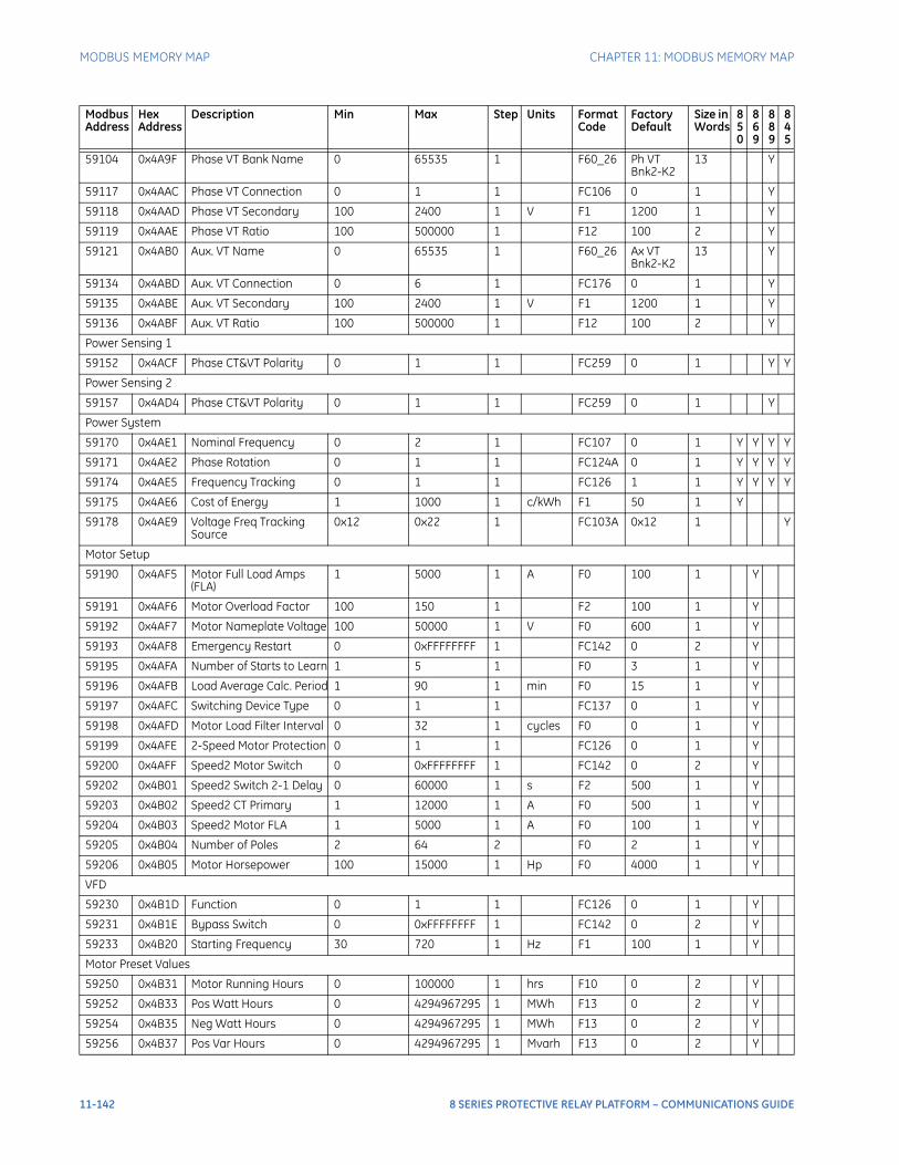
MODBUS MEMORY MAP CHAPTER 11: MODBUS MEMORY MAP
59104 0x4A9F Phase VT Bank Name 0 65535 1 F60_26 Ph VT Bnk2-K2
13 Y
59117 0x4AAC Phase VT Connection 0 1 1 FC106 0 1 Y
59118 0x4AAD Phase VT Secondary 100 2400 1 V F1 1200 1 Y
59119 0x4AAE Phase VT Ratio 100 500000 1 F12 100 2 Y
59121 0x4AB0 Aux. VT Name 0 65535 1 F60_26 Ax VT Bnk2-K2
13 Y
59134 0x4ABD Aux. VT Connection 0 6 1 FC176 0 1 Y
59135 0x4ABE Aux. VT Secondary 100 2400 1 V F1 1200 1 Y
59136 0x4ABF Aux. VT Ratio 100 500000 1 F12 100 2 Y
Power Sensing 1
59152 0x4ACF Phase CT&VT Polarity 0 1 1 FC259 0 1 Y Y
Power Sensing 2
59157 0x4AD4 Phase CT&VT Polarity 0 1 1 FC259 0 1 Y
Power System
59170 0x4AE1 Nominal Frequency 0 2 1 FC107 0 1 Y Y Y Y
59171 0x4AE2 Phase Rotation 0 1 1 FC124A 0 1 Y Y Y Y
59174 0x4AE5 Frequency Tracking 0 1 1 FC126 1 1 Y Y Y Y
59175 0x4AE6 Cost of Energy 1 1000 1 c/kWh F1 50 1 Y
59178 0x4AE9 Voltage Freq Tracking Source
0x12 0x22 1 FC103A 0x12 1 Y
Motor Setup
59190 0x4AF5 Motor Full Load Amps (FLA)
1 5000 1 A F0 100 1 Y
59191 0x4AF6 Motor Overload Factor 100 150 1 F2 100 1 Y
59192 0x4AF7 Motor Nameplate Voltage 100 50000 1 V F0 600 1 Y
59193 0x4AF8 Emergency Restart 0 0xFFFFFFFF 1 FC142 0 2 Y
59195 0x4AFA Number of Starts to Learn 1 5 1 F0 3 1 Y
59196 0x4AFB Load Average Calc. Period 1 90 1 min F0 15 1 Y
59197 0x4AFC Switching Device Type 0 1 1 FC137 0 1 Y
59198 0x4AFD Motor Load Filter Interval 0 32 1 cycles F0 0 1 Y
59199 0x4AFE 2-Speed Motor Protection 0 1 1 FC126 0 1 Y
59200 0x4AFF Speed2 Motor Switch 0 0xFFFFFFFF 1 FC142 0 2 Y
59202 0x4B01 Speed2 Switch 2-1 Delay 0 60000 1 s F2 500 1 Y
59203 0x4B02 Speed2 CT Primary 1 12000 1 A F0 500 1 Y
59204 0x4B03 Speed2 Motor FLA 1 5000 1 A F0 100 1 Y
59205 0x4B04 Number of Poles 2 64 2 F0 2 1 Y
59206 0x4B05 Motor Horsepower 100 15000 1 Hp F0 4000 1 Y
VFD
59230 0x4B1D Function 0 1 1 FC126 0 1 Y
59231 0x4B1E Bypass Switch 0 0xFFFFFFFF 1 FC142 0 2 Y
59233 0x4B20 Starting Frequency 30 720 1 Hz F1 100 1 Y
Motor Preset Values
59250 0x4B31 Motor Running Hours 0 100000 1 hrs F10 0 2 Y
59252 0x4B33 Pos Watt Hours 0 4294967295 1 MWh F13 0 2 Y
59254 0x4B35 Neg Watt Hours 0 4294967295 1 MWh F13 0 2 Y
59256 0x4B37 Pos Var Hours 0 4294967295 1 Mvarh F13 0 2 Y
Modbus Address
Hex Address
Description Min Max Step Units Format Code
Factory Default
Size in Words
850
869
889
845
11-142 8 SERIES PROTECTIVE RELAY PLATFORM – COMMUNICATIONS GUIDE
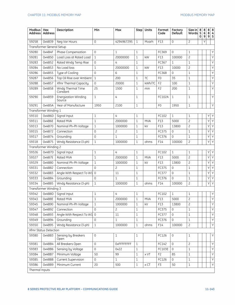
CHAPTER 11: MODBUS MEMORY MAP MODBUS MEMORY MAP
59258 0x4B39 Neg Var Hours 0 4294967295 1 Mvarh F13 0 2 Y
Transformer General Setup
59280 0x4B4F Phase Compensation 0 1 1 FC369 0 1 Y
59281 0x4B50 Load Loss at Rated Load 1 20000000 1 kW F13 100000 2 Y
59283 0x4B52 Rated Wndg Temp Rise 0 4 1 FC367 1 1 Y
59284 0x4B53 No Load loss 1 20000000 1 kW F13 10000 2 Y
59286 0x4B55 Type of Cooling 0 6 1 FC368 0 1 Y
59287 0x4B56 Top Oil Rise over Ambient 1 200 1 ?C F0 35 1 Y
59288 0x4B57 Xfmr Thermal Capacity 0 20000 1 kWh/?C F2 100 1 Y
59289 0x4B58 Wndg Thermal Time Constant
25 1500 1 min F2 200 1 Y
59290 0x4B59 Energization Winding Source
1 4 1 FC102A 1 1 Y
59291 0x4B5A Year of Manufacture 1950 2100 1 F0 1950 1 Y
Transformer Winding 1
59310 0x4B6D Signal Input 1 4 1 FC102 1 1 Y Y
59311 0x4B6E Rated MVA 1 2000000 1 MVA F13 5000 2 Y Y
59313 0x4B70 Nominal Ph-Ph Voltage 1 1000000 1 kV F13 13800 2 Y Y
59315 0x4B72 Connection 0 2 1 FC375 0 1 Y Y
59317 0x4B74 Grounding 0 1 1 FC376 0 1 Y Y
59318 0x4B75 Wndg Resistance (3-ph) 1 1000000 1 ohms F14 100000 2 Y Y
Transformer Winding 2
59326 0x4B7D Signal Input 1 4 1 FC102 1 1 Y Y
59327 0x4B7E Rated MVA 1 2000000 1 MVA F13 5000 2 Y Y
59329 0x4B80 Nominal Ph-Ph Voltage 1 1000000 1 kV F13 13800 2 Y Y
59331 0x4B82 Connection 0 2 1 FC375 0 1 Y Y
59332 0x4B83 Angle With Respect To W1 0 11 1 FC377 0 1 Y Y
59333 0x4B84 Grounding 0 1 1 FC376 0 1 Y Y
59334 0x4B85 Wndg Resistance (3-ph) 1 1000000 1 ohms F14 100000 2 Y Y
Transformer Winding 3
59342 0x4B8D Signal Input 1 4 1 FC102 1 1 Y
59343 0x4B8E Rated MVA 1 2000000 1 MVA F13 5000 2 Y
59345 0x4B90 Nominal Ph-Ph Voltage 1 1000000 1 kV F13 13800 2 Y
59347 0x4B92 Connection 0 2 1 FC375 0 1 Y
59348 0x4B93 Angle With Respect To W1 0 11 1 FC377 0 1 Y
59349 0x4B94 Grounding 0 1 1 FC376 0 1 Y
59350 0x4B95 Wndg Resistance (3-ph) 1 1000000 1 ohms F14 100000 2 Y
Xfmr Status Detection
59380 0x4BB3 Sensing by Breakers Open
0 1 1 FC126 0 1 Y
59381 0x4BB4 All Breakers Open 0 0xFFFFFFFF 1 FC142 0 2 Y
59383 0x4BB6 Sensing by Voltage 0 0x22 1 FC103E 0 1 Y
59384 0x4BB7 Minimum Voltage 50 99 1 x VT F2 85 1 Y
59385 0x4BB8 Current Supervision 0 1 1 FC126 0 1 Y
59386 0x4BB9 Minimum Current 20 500 1 x CT F3 50 1 Y
Thermal Inputs
Modbus Address
Hex Address
Description Min Max Step Units Format Code
Factory Default
Size in Words
850
869
889
845
8 SERIES PROTECTIVE RELAY PLATFORM – COMMUNICATIONS GUIDE 11-143
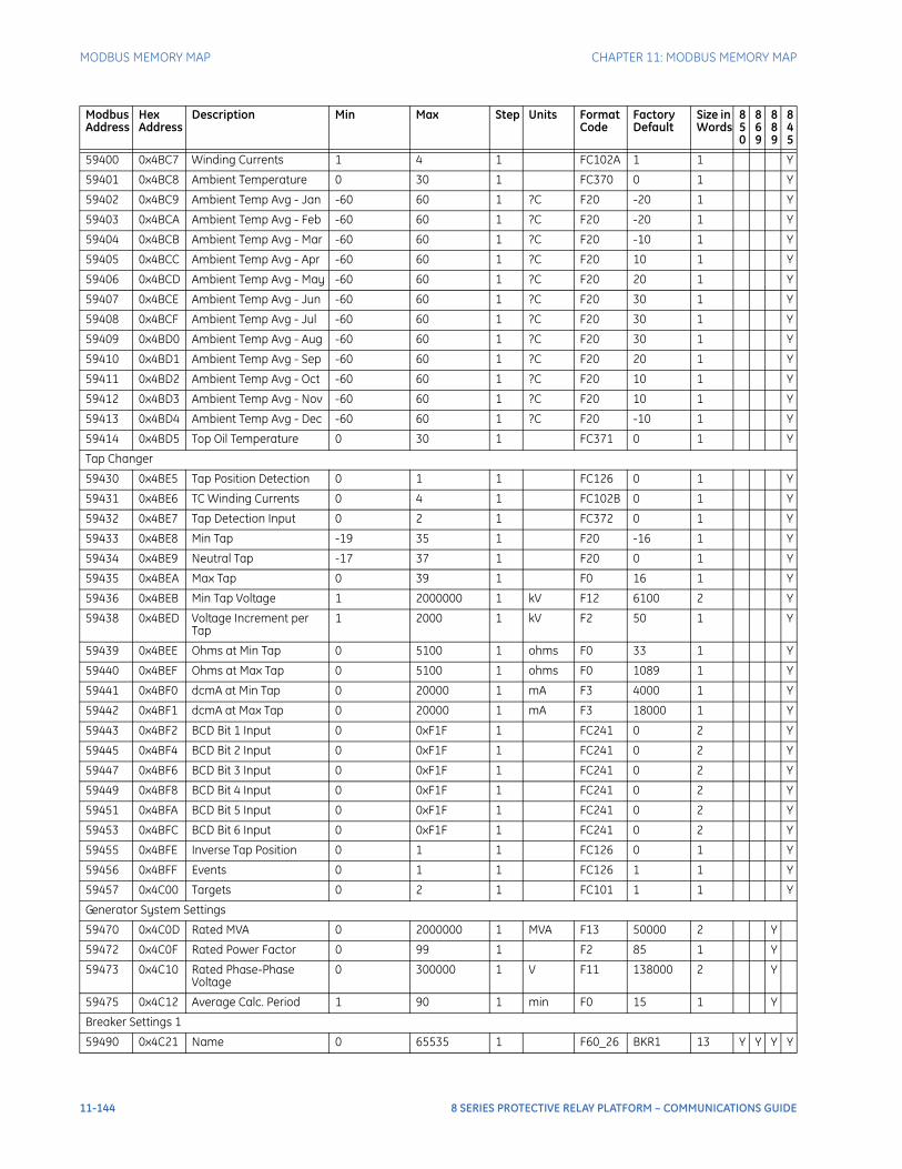
MODBUS MEMORY MAP CHAPTER 11: MODBUS MEMORY MAP
59400 0x4BC7 Winding Currents 1 4 1 FC102A 1 1 Y
59401 0x4BC8 Ambient Temperature 0 30 1 FC370 0 1 Y
59402 0x4BC9 Ambient Temp Avg - Jan -60 60 1 ?C F20 -20 1 Y
59403 0x4BCA Ambient Temp Avg - Feb -60 60 1 ?C F20 -20 1 Y
59404 0x4BCB Ambient Temp Avg - Mar -60 60 1 ?C F20 -10 1 Y
59405 0x4BCC Ambient Temp Avg - Apr -60 60 1 ?C F20 10 1 Y
59406 0x4BCD Ambient Temp Avg - May -60 60 1 ?C F20 20 1 Y
59407 0x4BCE Ambient Temp Avg - Jun -60 60 1 ?C F20 30 1 Y
59408 0x4BCF Ambient Temp Avg - Jul -60 60 1 ?C F20 30 1 Y
59409 0x4BD0 Ambient Temp Avg - Aug -60 60 1 ?C F20 30 1 Y
59410 0x4BD1 Ambient Temp Avg - Sep -60 60 1 ?C F20 20 1 Y
59411 0x4BD2 Ambient Temp Avg - Oct -60 60 1 ?C F20 10 1 Y
59412 0x4BD3 Ambient Temp Avg - Nov -60 60 1 ?C F20 10 1 Y
59413 0x4BD4 Ambient Temp Avg - Dec -60 60 1 ?C F20 -10 1 Y
59414 0x4BD5 Top Oil Temperature 0 30 1 FC371 0 1 Y
Tap Changer
59430 0x4BE5 Tap Position Detection 0 1 1 FC126 0 1 Y
59431 0x4BE6 TC Winding Currents 0 4 1 FC102B 0 1 Y
59432 0x4BE7 Tap Detection Input 0 2 1 FC372 0 1 Y
59433 0x4BE8 Min Tap -19 35 1 F20 -16 1 Y
59434 0x4BE9 Neutral Tap -17 37 1 F20 0 1 Y
59435 0x4BEA Max Tap 0 39 1 F0 16 1 Y
59436 0x4BEB Min Tap Voltage 1 2000000 1 kV F12 6100 2 Y
59438 0x4BED Voltage Increment per Tap
1 2000 1 kV F2 50 1 Y
59439 0x4BEE Ohms at Min Tap 0 5100 1 ohms F0 33 1 Y
59440 0x4BEF Ohms at Max Tap 0 5100 1 ohms F0 1089 1 Y
59441 0x4BF0 dcmA at Min Tap 0 20000 1 mA F3 4000 1 Y
59442 0x4BF1 dcmA at Max Tap 0 20000 1 mA F3 18000 1 Y
59443 0x4BF2 BCD Bit 1 Input 0 0xF1F 1 FC241 0 2 Y
59445 0x4BF4 BCD Bit 2 Input 0 0xF1F 1 FC241 0 2 Y
59447 0x4BF6 BCD Bit 3 Input 0 0xF1F 1 FC241 0 2 Y
59449 0x4BF8 BCD Bit 4 Input 0 0xF1F 1 FC241 0 2 Y
59451 0x4BFA BCD Bit 5 Input 0 0xF1F 1 FC241 0 2 Y
59453 0x4BFC BCD Bit 6 Input 0 0xF1F 1 FC241 0 2 Y
59455 0x4BFE Inverse Tap Position 0 1 1 FC126 0 1 Y
59456 0x4BFF Events 0 1 1 FC126 1 1 Y
59457 0x4C00 Targets 0 2 1 FC101 1 1 Y
Generator System Settings
59470 0x4C0D Rated MVA 0 2000000 1 MVA F13 50000 2 Y
59472 0x4C0F Rated Power Factor 0 99 1 F2 85 1 Y
59473 0x4C10 Rated Phase-Phase Voltage
0 300000 1 V F11 138000 2 Y
59475 0x4C12 Average Calc. Period 1 90 1 min F0 15 1 Y
Breaker Settings 1
59490 0x4C21 Name 0 65535 1 F60_26 BKR1 13 Y Y Y Y
Modbus Address
Hex Address
Description Min Max Step Units Format Code
Factory Default
Size in Words
850
869
889
845
11-144 8 SERIES PROTECTIVE RELAY PLATFORM – COMMUNICATIONS GUIDE

CHAPTER 11: MODBUS MEMORY MAP MODBUS MEMORY MAP
59503 0x4C2E Contact Input 52a 0 0x21F 1 FC266 0 2 Y Y Y Y
59505 0x4C30 Contact Input 52b 0 0x21F 1 FC266 0 2 Y Y Y Y
59507 0x4C32 Connected 0 0x21F 1 FC266 0 2 Y Y Y Y
59509 0x4C34 Trip Relay Select 0 0xFFFFFFFF 1 FC198F 1 2 Y Y
59511 0x4C36 Close Relay Select 0 0xFFFFFFFF 1 FC198G 2 2 Y Y Y Y
Breaker Settings 2
59523 0x4C42 Name 0 65535 1 F60_26 BKR2 13 Y Y
59536 0x4C4F Contact Input 52a 0 0x21F 1 FC266 0 2 Y Y
59538 0x4C51 Contact Input 52b 0 0x21F 1 FC266 0 2 Y Y
59540 0x4C53 Connected 0 0x21F 1 FC266 0 2 Y Y
59542 0x4C55 Trip Relay Select 0 0xFFFFFFFF 1 FC198F 0 2 Y Y
59544 0x4C57 Close Relay Select 0 0xFFFFFFFF 1 FC198G 0 2 Y Y
Breaker Settings 3
59556 0x4C63 Name 0 65535 1 F60_26 BKR3 13 Y
59569 0x4C70 Contact Input 52a 0 0x21F 1 FC266 0 2 Y
59571 0x4C72 Contact Input 52b 0 0x21F 1 FC266 0 2 Y
59573 0x4C74 Connected 0 0x21F 1 FC266 0 2 Y
59575 0x4C76 Trip Relay Select 0 0xFFFFFFFF 1 FC198F 0 2 Y
59577 0x4C78 Close Relay Select 0 0xFFFFFFFF 1 FC198G 0 2 Y
FlexCurve 1
59610 0x4C99 FlexCurve Name 0 65535 1 F60_26 FlexCurve A
13 Y Y Y Y
59623 0x4CA6 FlexCurve A Time 0.00xPKP
0 6000000 1 ms F10 0 2 Y Y Y Y
59625 0x4CA8 FlexCurve A Time 0.05xPKP
0 6000000 1 ms F10 0 2 Y Y Y Y
59627 0x4CAA FlexCurve A Time 0.10xPKP
0 6000000 1 ms F10 0 2 Y Y Y Y
59629 0x4CAC FlexCurve A Time 0.15xPKP
0 6000000 1 ms F10 0 2 Y Y Y Y
59631 0x4CAE FlexCurve A Time 0.20xPKP
0 6000000 1 ms F10 0 2 Y Y Y Y
59633 0x4CB0 FlexCurve A Time 0.25xPKP
0 6000000 1 ms F10 0 2 Y Y Y Y
59635 0x4CB2 FlexCurve A Time 0.30xPKP
0 6000000 1 ms F10 0 2 Y Y Y Y
59637 0x4CB4 FlexCurve A Time 0.35xPKP
0 6000000 1 ms F10 0 2 Y Y Y Y
59639 0x4CB6 FlexCurve A Time 0.40xPKP
0 6000000 1 ms F10 0 2 Y Y Y Y
59641 0x4CB8 FlexCurve A Time 0.45xPKP
0 6000000 1 ms F10 0 2 Y Y Y Y
59643 0x4CBA FlexCurve A Time 0.48xPKP
0 6000000 1 ms F10 0 2 Y Y Y Y
59645 0x4CBC FlexCurve A Time 0.50xPKP
0 6000000 1 ms F10 0 2 Y Y Y Y
59647 0x4CBE FlexCurve A Time 0.52xPKP
0 6000000 1 ms F10 0 2 Y Y Y Y
59649 0x4CC0 FlexCurve A Time 0.54xPKP
0 6000000 1 ms F10 0 2 Y Y Y Y
Modbus Address
Hex Address
Description Min Max Step Units Format Code
Factory Default
Size in Words
850
869
889
845
8 SERIES PROTECTIVE RELAY PLATFORM – COMMUNICATIONS GUIDE 11-145

MODBUS MEMORY MAP CHAPTER 11: MODBUS MEMORY MAP
59651 0x4CC2 FlexCurve A Time 0.56xPKP
0 6000000 1 ms F10 0 2 Y Y Y Y
59653 0x4CC4 FlexCurve A Time 0.58xPKP
0 6000000 1 ms F10 0 2 Y Y Y Y
59655 0x4CC6 FlexCurve A Time 0.60xPKP
0 6000000 1 ms F10 0 2 Y Y Y Y
59657 0x4CC8 FlexCurve A Time 0.62xPKP
0 6000000 1 ms F10 0 2 Y Y Y Y
59659 0x4CCA FlexCurve A Time 0.64xPKP
0 6000000 1 ms F10 0 2 Y Y Y Y
59661 0x4CCC FlexCurve A Time 0.66xPKP
0 6000000 1 ms F10 0 2 Y Y Y Y
59663 0x4CCE FlexCurve A Time 0.68xPKP
0 6000000 1 ms F10 0 2 Y Y Y Y
59665 0x4CD0 FlexCurve A Time 0.70xPKP
0 6000000 1 ms F10 0 2 Y Y Y Y
59667 0x4CD2 FlexCurve A Time 0.72xPKP
0 6000000 1 ms F10 0 2 Y Y Y Y
59669 0x4CD4 FlexCurve A Time 0.74xPKP
0 6000000 1 ms F10 0 2 Y Y Y Y
59671 0x4CD6 FlexCurve A Time 0.76xPKP
0 6000000 1 ms F10 0 2 Y Y Y Y
59673 0x4CD8 FlexCurve A Time 0.78xPKP
0 6000000 1 ms F10 0 2 Y Y Y Y
59675 0x4CDA FlexCurve A Time 0.80xPKP
0 6000000 1 ms F10 0 2 Y Y Y Y
59677 0x4CDC FlexCurve A Time 0.82xPKP
0 6000000 1 ms F10 0 2 Y Y Y Y
59679 0x4CDE FlexCurve A Time 0.84xPKP
0 6000000 1 ms F10 0 2 Y Y Y Y
59681 0x4CE0 FlexCurve A Time 0.86xPKP
0 6000000 1 ms F10 0 2 Y Y Y Y
59683 0x4CE2 FlexCurve A Time 0.88xPKP
0 6000000 1 ms F10 0 2 Y Y Y Y
59685 0x4CE4 FlexCurve A Time 0.90xPKP
0 6000000 1 ms F10 0 2 Y Y Y Y
59687 0x4CE6 FlexCurve A Time 0.91xPKP
0 6000000 1 ms F10 0 2 Y Y Y Y
59689 0x4CE8 FlexCurve A Time 0.92xPKP
0 6000000 1 ms F10 0 2 Y Y Y Y
59691 0x4CEA FlexCurve A Time 0.93xPKP
0 6000000 1 ms F10 0 2 Y Y Y Y
59693 0x4CEC FlexCurve A Time 0.94xPKP
0 6000000 1 ms F10 0 2 Y Y Y Y
59695 0x4CEE FlexCurve A Time 0.95xPKP
0 6000000 1 ms F10 0 2 Y Y Y Y
59697 0x4CF0 FlexCurve A Time 0.96xPKP
0 6000000 1 ms F10 0 2 Y Y Y Y
59699 0x4CF2 FlexCurve A Time 0.97xPKP
0 6000000 1 ms F10 0 2 Y Y Y Y
59701 0x4CF4 FlexCurve A Time 0.98xPKP
0 6000000 1 ms F10 0 2 Y Y Y Y
59703 0x4CF6 FlexCurve A Time 1.03xPKP
0 6000000 1 ms F10 0 2 Y Y Y Y
59705 0x4CF8 FlexCurve A Time 1.05xPKP
0 6000000 1 ms F10 0 2 Y Y Y Y
Modbus Address
Hex Address
Description Min Max Step Units Format Code
Factory Default
Size in Words
850
869
889
845
11-146 8 SERIES PROTECTIVE RELAY PLATFORM – COMMUNICATIONS GUIDE
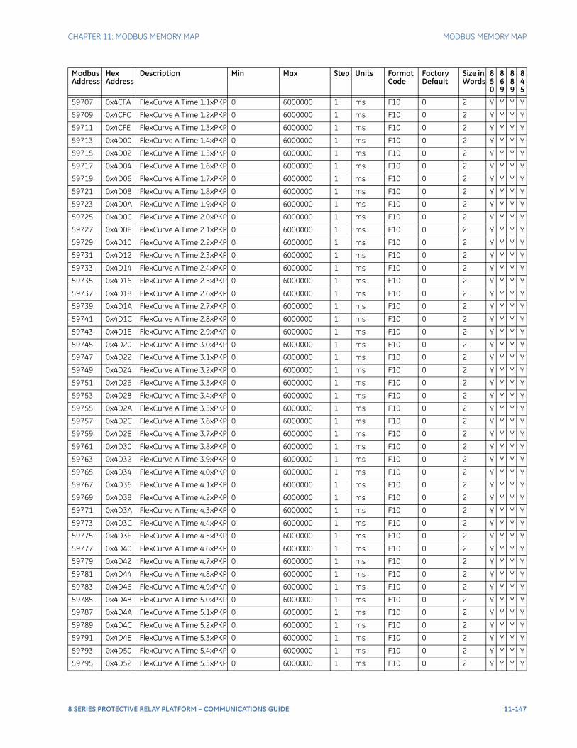
CHAPTER 11: MODBUS MEMORY MAP MODBUS MEMORY MAP
59707 0x4CFA FlexCurve A Time 1.1xPKP 0 6000000 1 ms F10 0 2 Y Y Y Y
59709 0x4CFC FlexCurve A Time 1.2xPKP 0 6000000 1 ms F10 0 2 Y Y Y Y
59711 0x4CFE FlexCurve A Time 1.3xPKP 0 6000000 1 ms F10 0 2 Y Y Y Y
59713 0x4D00 FlexCurve A Time 1.4xPKP 0 6000000 1 ms F10 0 2 Y Y Y Y
59715 0x4D02 FlexCurve A Time 1.5xPKP 0 6000000 1 ms F10 0 2 Y Y Y Y
59717 0x4D04 FlexCurve A Time 1.6xPKP 0 6000000 1 ms F10 0 2 Y Y Y Y
59719 0x4D06 FlexCurve A Time 1.7xPKP 0 6000000 1 ms F10 0 2 Y Y Y Y
59721 0x4D08 FlexCurve A Time 1.8xPKP 0 6000000 1 ms F10 0 2 Y Y Y Y
59723 0x4D0A FlexCurve A Time 1.9xPKP 0 6000000 1 ms F10 0 2 Y Y Y Y
59725 0x4D0C FlexCurve A Time 2.0xPKP 0 6000000 1 ms F10 0 2 Y Y Y Y
59727 0x4D0E FlexCurve A Time 2.1xPKP 0 6000000 1 ms F10 0 2 Y Y Y Y
59729 0x4D10 FlexCurve A Time 2.2xPKP 0 6000000 1 ms F10 0 2 Y Y Y Y
59731 0x4D12 FlexCurve A Time 2.3xPKP 0 6000000 1 ms F10 0 2 Y Y Y Y
59733 0x4D14 FlexCurve A Time 2.4xPKP 0 6000000 1 ms F10 0 2 Y Y Y Y
59735 0x4D16 FlexCurve A Time 2.5xPKP 0 6000000 1 ms F10 0 2 Y Y Y Y
59737 0x4D18 FlexCurve A Time 2.6xPKP 0 6000000 1 ms F10 0 2 Y Y Y Y
59739 0x4D1A FlexCurve A Time 2.7xPKP 0 6000000 1 ms F10 0 2 Y Y Y Y
59741 0x4D1C FlexCurve A Time 2.8xPKP 0 6000000 1 ms F10 0 2 Y Y Y Y
59743 0x4D1E FlexCurve A Time 2.9xPKP 0 6000000 1 ms F10 0 2 Y Y Y Y
59745 0x4D20 FlexCurve A Time 3.0xPKP 0 6000000 1 ms F10 0 2 Y Y Y Y
59747 0x4D22 FlexCurve A Time 3.1xPKP 0 6000000 1 ms F10 0 2 Y Y Y Y
59749 0x4D24 FlexCurve A Time 3.2xPKP 0 6000000 1 ms F10 0 2 Y Y Y Y
59751 0x4D26 FlexCurve A Time 3.3xPKP 0 6000000 1 ms F10 0 2 Y Y Y Y
59753 0x4D28 FlexCurve A Time 3.4xPKP 0 6000000 1 ms F10 0 2 Y Y Y Y
59755 0x4D2A FlexCurve A Time 3.5xPKP 0 6000000 1 ms F10 0 2 Y Y Y Y
59757 0x4D2C FlexCurve A Time 3.6xPKP 0 6000000 1 ms F10 0 2 Y Y Y Y
59759 0x4D2E FlexCurve A Time 3.7xPKP 0 6000000 1 ms F10 0 2 Y Y Y Y
59761 0x4D30 FlexCurve A Time 3.8xPKP 0 6000000 1 ms F10 0 2 Y Y Y Y
59763 0x4D32 FlexCurve A Time 3.9xPKP 0 6000000 1 ms F10 0 2 Y Y Y Y
59765 0x4D34 FlexCurve A Time 4.0xPKP 0 6000000 1 ms F10 0 2 Y Y Y Y
59767 0x4D36 FlexCurve A Time 4.1xPKP 0 6000000 1 ms F10 0 2 Y Y Y Y
59769 0x4D38 FlexCurve A Time 4.2xPKP 0 6000000 1 ms F10 0 2 Y Y Y Y
59771 0x4D3A FlexCurve A Time 4.3xPKP 0 6000000 1 ms F10 0 2 Y Y Y Y
59773 0x4D3C FlexCurve A Time 4.4xPKP 0 6000000 1 ms F10 0 2 Y Y Y Y
59775 0x4D3E FlexCurve A Time 4.5xPKP 0 6000000 1 ms F10 0 2 Y Y Y Y
59777 0x4D40 FlexCurve A Time 4.6xPKP 0 6000000 1 ms F10 0 2 Y Y Y Y
59779 0x4D42 FlexCurve A Time 4.7xPKP 0 6000000 1 ms F10 0 2 Y Y Y Y
59781 0x4D44 FlexCurve A Time 4.8xPKP 0 6000000 1 ms F10 0 2 Y Y Y Y
59783 0x4D46 FlexCurve A Time 4.9xPKP 0 6000000 1 ms F10 0 2 Y Y Y Y
59785 0x4D48 FlexCurve A Time 5.0xPKP 0 6000000 1 ms F10 0 2 Y Y Y Y
59787 0x4D4A FlexCurve A Time 5.1xPKP 0 6000000 1 ms F10 0 2 Y Y Y Y
59789 0x4D4C FlexCurve A Time 5.2xPKP 0 6000000 1 ms F10 0 2 Y Y Y Y
59791 0x4D4E FlexCurve A Time 5.3xPKP 0 6000000 1 ms F10 0 2 Y Y Y Y
59793 0x4D50 FlexCurve A Time 5.4xPKP 0 6000000 1 ms F10 0 2 Y Y Y Y
59795 0x4D52 FlexCurve A Time 5.5xPKP 0 6000000 1 ms F10 0 2 Y Y Y Y
Modbus Address
Hex Address
Description Min Max Step Units Format Code
Factory Default
Size in Words
850
869
889
845
8 SERIES PROTECTIVE RELAY PLATFORM – COMMUNICATIONS GUIDE 11-147
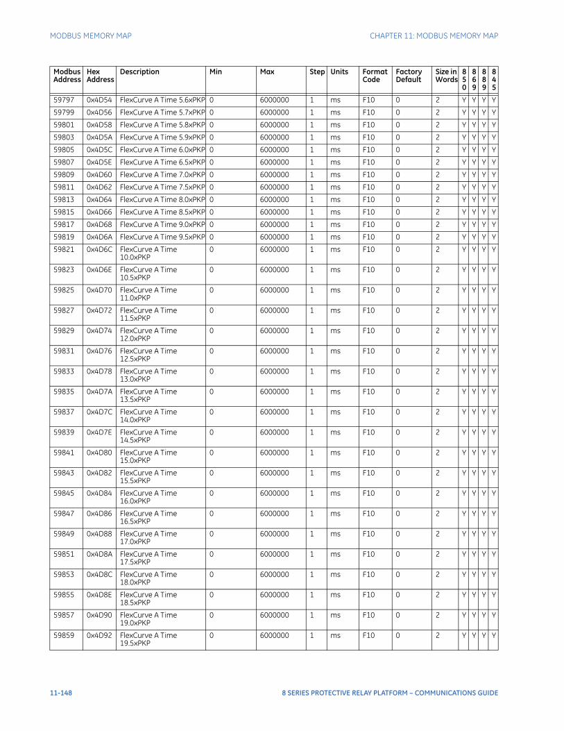
MODBUS MEMORY MAP CHAPTER 11: MODBUS MEMORY MAP
59797 0x4D54 FlexCurve A Time 5.6xPKP 0 6000000 1 ms F10 0 2 Y Y Y Y
59799 0x4D56 FlexCurve A Time 5.7xPKP 0 6000000 1 ms F10 0 2 Y Y Y Y
59801 0x4D58 FlexCurve A Time 5.8xPKP 0 6000000 1 ms F10 0 2 Y Y Y Y
59803 0x4D5A FlexCurve A Time 5.9xPKP 0 6000000 1 ms F10 0 2 Y Y Y Y
59805 0x4D5C FlexCurve A Time 6.0xPKP 0 6000000 1 ms F10 0 2 Y Y Y Y
59807 0x4D5E FlexCurve A Time 6.5xPKP 0 6000000 1 ms F10 0 2 Y Y Y Y
59809 0x4D60 FlexCurve A Time 7.0xPKP 0 6000000 1 ms F10 0 2 Y Y Y Y
59811 0x4D62 FlexCurve A Time 7.5xPKP 0 6000000 1 ms F10 0 2 Y Y Y Y
59813 0x4D64 FlexCurve A Time 8.0xPKP 0 6000000 1 ms F10 0 2 Y Y Y Y
59815 0x4D66 FlexCurve A Time 8.5xPKP 0 6000000 1 ms F10 0 2 Y Y Y Y
59817 0x4D68 FlexCurve A Time 9.0xPKP 0 6000000 1 ms F10 0 2 Y Y Y Y
59819 0x4D6A FlexCurve A Time 9.5xPKP 0 6000000 1 ms F10 0 2 Y Y Y Y
59821 0x4D6C FlexCurve A Time 10.0xPKP
0 6000000 1 ms F10 0 2 Y Y Y Y
59823 0x4D6E FlexCurve A Time 10.5xPKP
0 6000000 1 ms F10 0 2 Y Y Y Y
59825 0x4D70 FlexCurve A Time 11.0xPKP
0 6000000 1 ms F10 0 2 Y Y Y Y
59827 0x4D72 FlexCurve A Time 11.5xPKP
0 6000000 1 ms F10 0 2 Y Y Y Y
59829 0x4D74 FlexCurve A Time 12.0xPKP
0 6000000 1 ms F10 0 2 Y Y Y Y
59831 0x4D76 FlexCurve A Time 12.5xPKP
0 6000000 1 ms F10 0 2 Y Y Y Y
59833 0x4D78 FlexCurve A Time 13.0xPKP
0 6000000 1 ms F10 0 2 Y Y Y Y
59835 0x4D7A FlexCurve A Time 13.5xPKP
0 6000000 1 ms F10 0 2 Y Y Y Y
59837 0x4D7C FlexCurve A Time 14.0xPKP
0 6000000 1 ms F10 0 2 Y Y Y Y
59839 0x4D7E FlexCurve A Time 14.5xPKP
0 6000000 1 ms F10 0 2 Y Y Y Y
59841 0x4D80 FlexCurve A Time 15.0xPKP
0 6000000 1 ms F10 0 2 Y Y Y Y
59843 0x4D82 FlexCurve A Time 15.5xPKP
0 6000000 1 ms F10 0 2 Y Y Y Y
59845 0x4D84 FlexCurve A Time 16.0xPKP
0 6000000 1 ms F10 0 2 Y Y Y Y
59847 0x4D86 FlexCurve A Time 16.5xPKP
0 6000000 1 ms F10 0 2 Y Y Y Y
59849 0x4D88 FlexCurve A Time 17.0xPKP
0 6000000 1 ms F10 0 2 Y Y Y Y
59851 0x4D8A FlexCurve A Time 17.5xPKP
0 6000000 1 ms F10 0 2 Y Y Y Y
59853 0x4D8C FlexCurve A Time 18.0xPKP
0 6000000 1 ms F10 0 2 Y Y Y Y
59855 0x4D8E FlexCurve A Time 18.5xPKP
0 6000000 1 ms F10 0 2 Y Y Y Y
59857 0x4D90 FlexCurve A Time 19.0xPKP
0 6000000 1 ms F10 0 2 Y Y Y Y
59859 0x4D92 FlexCurve A Time 19.5xPKP
0 6000000 1 ms F10 0 2 Y Y Y Y
Modbus Address
Hex Address
Description Min Max Step Units Format Code
Factory Default
Size in Words
850
869
889
845
11-148 8 SERIES PROTECTIVE RELAY PLATFORM – COMMUNICATIONS GUIDE
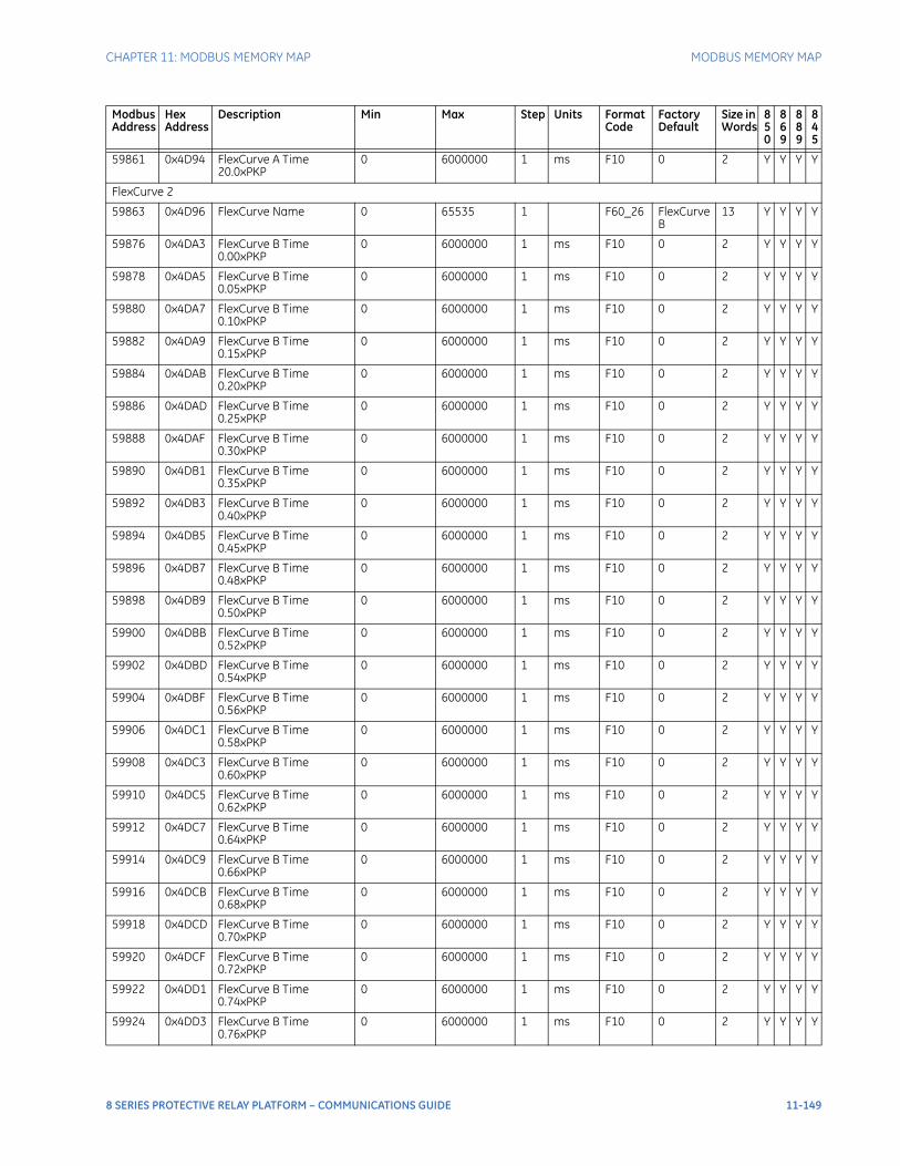
CHAPTER 11: MODBUS MEMORY MAP MODBUS MEMORY MAP
59861 0x4D94 FlexCurve A Time 20.0xPKP
0 6000000 1 ms F10 0 2 Y Y Y Y
FlexCurve 2
59863 0x4D96 FlexCurve Name 0 65535 1 F60_26 FlexCurve B
13 Y Y Y Y
59876 0x4DA3 FlexCurve B Time 0.00xPKP
0 6000000 1 ms F10 0 2 Y Y Y Y
59878 0x4DA5 FlexCurve B Time 0.05xPKP
0 6000000 1 ms F10 0 2 Y Y Y Y
59880 0x4DA7 FlexCurve B Time 0.10xPKP
0 6000000 1 ms F10 0 2 Y Y Y Y
59882 0x4DA9 FlexCurve B Time 0.15xPKP
0 6000000 1 ms F10 0 2 Y Y Y Y
59884 0x4DAB FlexCurve B Time 0.20xPKP
0 6000000 1 ms F10 0 2 Y Y Y Y
59886 0x4DAD FlexCurve B Time 0.25xPKP
0 6000000 1 ms F10 0 2 Y Y Y Y
59888 0x4DAF FlexCurve B Time 0.30xPKP
0 6000000 1 ms F10 0 2 Y Y Y Y
59890 0x4DB1 FlexCurve B Time 0.35xPKP
0 6000000 1 ms F10 0 2 Y Y Y Y
59892 0x4DB3 FlexCurve B Time 0.40xPKP
0 6000000 1 ms F10 0 2 Y Y Y Y
59894 0x4DB5 FlexCurve B Time 0.45xPKP
0 6000000 1 ms F10 0 2 Y Y Y Y
59896 0x4DB7 FlexCurve B Time 0.48xPKP
0 6000000 1 ms F10 0 2 Y Y Y Y
59898 0x4DB9 FlexCurve B Time 0.50xPKP
0 6000000 1 ms F10 0 2 Y Y Y Y
59900 0x4DBB FlexCurve B Time 0.52xPKP
0 6000000 1 ms F10 0 2 Y Y Y Y
59902 0x4DBD FlexCurve B Time 0.54xPKP
0 6000000 1 ms F10 0 2 Y Y Y Y
59904 0x4DBF FlexCurve B Time 0.56xPKP
0 6000000 1 ms F10 0 2 Y Y Y Y
59906 0x4DC1 FlexCurve B Time 0.58xPKP
0 6000000 1 ms F10 0 2 Y Y Y Y
59908 0x4DC3 FlexCurve B Time 0.60xPKP
0 6000000 1 ms F10 0 2 Y Y Y Y
59910 0x4DC5 FlexCurve B Time 0.62xPKP
0 6000000 1 ms F10 0 2 Y Y Y Y
59912 0x4DC7 FlexCurve B Time 0.64xPKP
0 6000000 1 ms F10 0 2 Y Y Y Y
59914 0x4DC9 FlexCurve B Time 0.66xPKP
0 6000000 1 ms F10 0 2 Y Y Y Y
59916 0x4DCB FlexCurve B Time 0.68xPKP
0 6000000 1 ms F10 0 2 Y Y Y Y
59918 0x4DCD FlexCurve B Time 0.70xPKP
0 6000000 1 ms F10 0 2 Y Y Y Y
59920 0x4DCF FlexCurve B Time 0.72xPKP
0 6000000 1 ms F10 0 2 Y Y Y Y
59922 0x4DD1 FlexCurve B Time 0.74xPKP
0 6000000 1 ms F10 0 2 Y Y Y Y
59924 0x4DD3 FlexCurve B Time 0.76xPKP
0 6000000 1 ms F10 0 2 Y Y Y Y
Modbus Address
Hex Address
Description Min Max Step Units Format Code
Factory Default
Size in Words
850
869
889
845
8 SERIES PROTECTIVE RELAY PLATFORM – COMMUNICATIONS GUIDE 11-149
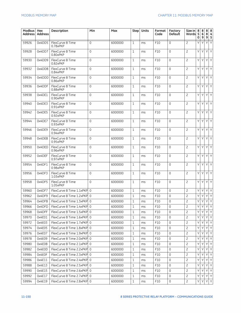
MODBUS MEMORY MAP CHAPTER 11: MODBUS MEMORY MAP
59926 0x4DD5 FlexCurve B Time 0.78xPKP
0 6000000 1 ms F10 0 2 Y Y Y Y
59928 0x4DD7 FlexCurve B Time 0.80xPKP
0 6000000 1 ms F10 0 2 Y Y Y Y
59930 0x4DD9 FlexCurve B Time 0.82xPKP
0 6000000 1 ms F10 0 2 Y Y Y Y
59932 0x4DDB FlexCurve B Time 0.84xPKP
0 6000000 1 ms F10 0 2 Y Y Y Y
59934 0x4DDD FlexCurve B Time 0.86xPKP
0 6000000 1 ms F10 0 2 Y Y Y Y
59936 0x4DDF FlexCurve B Time 0.88xPKP
0 6000000 1 ms F10 0 2 Y Y Y Y
59938 0x4DE1 FlexCurve B Time 0.90xPKP
0 6000000 1 ms F10 0 2 Y Y Y Y
59940 0x4DE3 FlexCurve B Time 0.91xPKP
0 6000000 1 ms F10 0 2 Y Y Y Y
59942 0x4DE5 FlexCurve B Time 0.92xPKP
0 6000000 1 ms F10 0 2 Y Y Y Y
59944 0x4DE7 FlexCurve B Time 0.93xPKP
0 6000000 1 ms F10 0 2 Y Y Y Y
59946 0x4DE9 FlexCurve B Time 0.94xPKP
0 6000000 1 ms F10 0 2 Y Y Y Y
59948 0x4DEB FlexCurve B Time 0.95xPKP
0 6000000 1 ms F10 0 2 Y Y Y Y
59950 0x4DED FlexCurve B Time 0.96xPKP
0 6000000 1 ms F10 0 2 Y Y Y Y
59952 0x4DEF FlexCurve B Time 0.97xPKP
0 6000000 1 ms F10 0 2 Y Y Y Y
59954 0x4DF1 FlexCurve B Time 0.98xPKP
0 6000000 1 ms F10 0 2 Y Y Y Y
59956 0x4DF3 FlexCurve B Time 1.03xPKP
0 6000000 1 ms F10 0 2 Y Y Y Y
59958 0x4DF5 FlexCurve B Time 1.05xPKP
0 6000000 1 ms F10 0 2 Y Y Y Y
59960 0x4DF7 FlexCurve B Time 1.1xPKP 0 6000000 1 ms F10 0 2 Y Y Y Y
59962 0x4DF9 FlexCurve B Time 1.2xPKP 0 6000000 1 ms F10 0 2 Y Y Y Y
59964 0x4DFB FlexCurve B Time 1.3xPKP 0 6000000 1 ms F10 0 2 Y Y Y Y
59966 0x4DFD FlexCurve B Time 1.4xPKP 0 6000000 1 ms F10 0 2 Y Y Y Y
59968 0x4DFF FlexCurve B Time 1.5xPKP 0 6000000 1 ms F10 0 2 Y Y Y Y
59970 0x4E01 FlexCurve B Time 1.6xPKP 0 6000000 1 ms F10 0 2 Y Y Y Y
59972 0x4E03 FlexCurve B Time 1.7xPKP 0 6000000 1 ms F10 0 2 Y Y Y Y
59974 0x4E05 FlexCurve B Time 1.8xPKP 0 6000000 1 ms F10 0 2 Y Y Y Y
59976 0x4E07 FlexCurve B Time 1.9xPKP 0 6000000 1 ms F10 0 2 Y Y Y Y
59978 0x4E09 FlexCurve B Time 2.0xPKP 0 6000000 1 ms F10 0 2 Y Y Y Y
59980 0x4E0B FlexCurve B Time 2.1xPKP 0 6000000 1 ms F10 0 2 Y Y Y Y
59982 0x4E0D FlexCurve B Time 2.2xPKP 0 6000000 1 ms F10 0 2 Y Y Y Y
59984 0x4E0F FlexCurve B Time 2.3xPKP 0 6000000 1 ms F10 0 2 Y Y Y Y
59986 0x4E11 FlexCurve B Time 2.4xPKP 0 6000000 1 ms F10 0 2 Y Y Y Y
59988 0x4E13 FlexCurve B Time 2.5xPKP 0 6000000 1 ms F10 0 2 Y Y Y Y
59990 0x4E15 FlexCurve B Time 2.6xPKP 0 6000000 1 ms F10 0 2 Y Y Y Y
59992 0x4E17 FlexCurve B Time 2.7xPKP 0 6000000 1 ms F10 0 2 Y Y Y Y
59994 0x4E19 FlexCurve B Time 2.8xPKP 0 6000000 1 ms F10 0 2 Y Y Y Y
Modbus Address
Hex Address
Description Min Max Step Units Format Code
Factory Default
Size in Words
850
869
889
845
11-150 8 SERIES PROTECTIVE RELAY PLATFORM – COMMUNICATIONS GUIDE
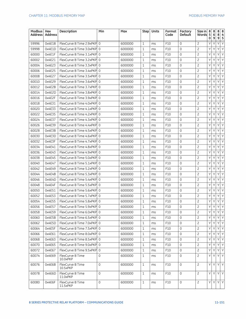
CHAPTER 11: MODBUS MEMORY MAP MODBUS MEMORY MAP
59996 0x4E1B FlexCurve B Time 2.9xPKP 0 6000000 1 ms F10 0 2 Y Y Y Y
59998 0x4E1D FlexCurve B Time 3.0xPKP 0 6000000 1 ms F10 0 2 Y Y Y Y
60000 0x4E1F FlexCurve B Time 3.1xPKP 0 6000000 1 ms F10 0 2 Y Y Y Y
60002 0x4E21 FlexCurve B Time 3.2xPKP 0 6000000 1 ms F10 0 2 Y Y Y Y
60004 0x4E23 FlexCurve B Time 3.3xPKP 0 6000000 1 ms F10 0 2 Y Y Y Y
60006 0x4E25 FlexCurve B Time 3.4xPKP 0 6000000 1 ms F10 0 2 Y Y Y Y
60008 0x4E27 FlexCurve B Time 3.5xPKP 0 6000000 1 ms F10 0 2 Y Y Y Y
60010 0x4E29 FlexCurve B Time 3.6xPKP 0 6000000 1 ms F10 0 2 Y Y Y Y
60012 0x4E2B FlexCurve B Time 3.7xPKP 0 6000000 1 ms F10 0 2 Y Y Y Y
60014 0x4E2D FlexCurve B Time 3.8xPKP 0 6000000 1 ms F10 0 2 Y Y Y Y
60016 0x4E2F FlexCurve B Time 3.9xPKP 0 6000000 1 ms F10 0 2 Y Y Y Y
60018 0x4E31 FlexCurve B Time 4.0xPKP 0 6000000 1 ms F10 0 2 Y Y Y Y
60020 0x4E33 FlexCurve B Time 4.1xPKP 0 6000000 1 ms F10 0 2 Y Y Y Y
60022 0x4E35 FlexCurve B Time 4.2xPKP 0 6000000 1 ms F10 0 2 Y Y Y Y
60024 0x4E37 FlexCurve B Time 4.3xPKP 0 6000000 1 ms F10 0 2 Y Y Y Y
60026 0x4E39 FlexCurve B Time 4.4xPKP 0 6000000 1 ms F10 0 2 Y Y Y Y
60028 0x4E3B FlexCurve B Time 4.5xPKP 0 6000000 1 ms F10 0 2 Y Y Y Y
60030 0x4E3D FlexCurve B Time 4.6xPKP 0 6000000 1 ms F10 0 2 Y Y Y Y
60032 0x4E3F FlexCurve B Time 4.7xPKP 0 6000000 1 ms F10 0 2 Y Y Y Y
60034 0x4E41 FlexCurve B Time 4.8xPKP 0 6000000 1 ms F10 0 2 Y Y Y Y
60036 0x4E43 FlexCurve B Time 4.9xPKP 0 6000000 1 ms F10 0 2 Y Y Y Y
60038 0x4E45 FlexCurve B Time 5.0xPKP 0 6000000 1 ms F10 0 2 Y Y Y Y
60040 0x4E47 FlexCurve B Time 5.1xPKP 0 6000000 1 ms F10 0 2 Y Y Y Y
60042 0x4E49 FlexCurve B Time 5.2xPKP 0 6000000 1 ms F10 0 2 Y Y Y Y
60044 0x4E4B FlexCurve B Time 5.3xPKP 0 6000000 1 ms F10 0 2 Y Y Y Y
60046 0x4E4D FlexCurve B Time 5.4xPKP 0 6000000 1 ms F10 0 2 Y Y Y Y
60048 0x4E4F FlexCurve B Time 5.5xPKP 0 6000000 1 ms F10 0 2 Y Y Y Y
60050 0x4E51 FlexCurve B Time 5.6xPKP 0 6000000 1 ms F10 0 2 Y Y Y Y
60052 0x4E53 FlexCurve B Time 5.7xPKP 0 6000000 1 ms F10 0 2 Y Y Y Y
60054 0x4E55 FlexCurve B Time 5.8xPKP 0 6000000 1 ms F10 0 2 Y Y Y Y
60056 0x4E57 FlexCurve B Time 5.9xPKP 0 6000000 1 ms F10 0 2 Y Y Y Y
60058 0x4E59 FlexCurve B Time 6.0xPKP 0 6000000 1 ms F10 0 2 Y Y Y Y
60060 0x4E5B FlexCurve B Time 6.5xPKP 0 6000000 1 ms F10 0 2 Y Y Y Y
60062 0x4E5D FlexCurve B Time 7.0xPKP 0 6000000 1 ms F10 0 2 Y Y Y Y
60064 0x4E5F FlexCurve B Time 7.5xPKP 0 6000000 1 ms F10 0 2 Y Y Y Y
60066 0x4E61 FlexCurve B Time 8.0xPKP 0 6000000 1 ms F10 0 2 Y Y Y Y
60068 0x4E63 FlexCurve B Time 8.5xPKP 0 6000000 1 ms F10 0 2 Y Y Y Y
60070 0x4E65 FlexCurve B Time 9.0xPKP 0 6000000 1 ms F10 0 2 Y Y Y Y
60072 0x4E67 FlexCurve B Time 9.5xPKP 0 6000000 1 ms F10 0 2 Y Y Y Y
60074 0x4E69 FlexCurve B Time 10.0xPKP
0 6000000 1 ms F10 0 2 Y Y Y Y
60076 0x4E6B FlexCurve B Time 10.5xPKP
0 6000000 1 ms F10 0 2 Y Y Y Y
60078 0x4E6D FlexCurve B Time 11.0xPKP
0 6000000 1 ms F10 0 2 Y Y Y Y
60080 0x4E6F FlexCurve B Time 11.5xPKP
0 6000000 1 ms F10 0 2 Y Y Y Y
Modbus Address
Hex Address
Description Min Max Step Units Format Code
Factory Default
Size in Words
850
869
889
845
8 SERIES PROTECTIVE RELAY PLATFORM – COMMUNICATIONS GUIDE 11-151
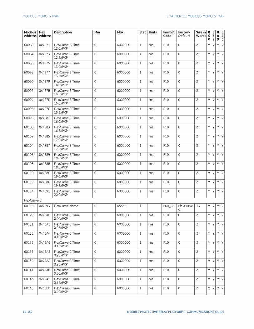
MODBUS MEMORY MAP CHAPTER 11: MODBUS MEMORY MAP
60082 0x4E71 FlexCurve B Time 12.0xPKP
0 6000000 1 ms F10 0 2 Y Y Y Y
60084 0x4E73 FlexCurve B Time 12.5xPKP
0 6000000 1 ms F10 0 2 Y Y Y Y
60086 0x4E75 FlexCurve B Time 13.0xPKP
0 6000000 1 ms F10 0 2 Y Y Y Y
60088 0x4E77 FlexCurve B Time 13.5xPKP
0 6000000 1 ms F10 0 2 Y Y Y Y
60090 0x4E79 FlexCurve B Time 14.0xPKP
0 6000000 1 ms F10 0 2 Y Y Y Y
60092 0x4E7B FlexCurve B Time 14.5xPKP
0 6000000 1 ms F10 0 2 Y Y Y Y
60094 0x4E7D FlexCurve B Time 15.0xPKP
0 6000000 1 ms F10 0 2 Y Y Y Y
60096 0x4E7F FlexCurve B Time 15.5xPKP
0 6000000 1 ms F10 0 2 Y Y Y Y
60098 0x4E81 FlexCurve B Time 16.0xPKP
0 6000000 1 ms F10 0 2 Y Y Y Y
60100 0x4E83 FlexCurve B Time 16.5xPKP
0 6000000 1 ms F10 0 2 Y Y Y Y
60102 0x4E85 FlexCurve B Time 17.0xPKP
0 6000000 1 ms F10 0 2 Y Y Y Y
60104 0x4E87 FlexCurve B Time 17.5xPKP
0 6000000 1 ms F10 0 2 Y Y Y Y
60106 0x4E89 FlexCurve B Time 18.0xPKP
0 6000000 1 ms F10 0 2 Y Y Y Y
60108 0x4E8B FlexCurve B Time 18.5xPKP
0 6000000 1 ms F10 0 2 Y Y Y Y
60110 0x4E8D FlexCurve B Time 19.0xPKP
0 6000000 1 ms F10 0 2 Y Y Y Y
60112 0x4E8F FlexCurve B Time 19.5xPKP
0 6000000 1 ms F10 0 2 Y Y Y Y
60114 0x4E91 FlexCurve B Time 20.0xPKP
0 6000000 1 ms F10 0 2 Y Y Y Y
FlexCurve 3
60116 0x4E93 FlexCurve Name 0 65535 1 F60_26 FlexCurve C
13 Y Y Y Y
60129 0x4EA0 FlexCurve C Time 0.00xPKP
0 6000000 1 ms F10 0 2 Y Y Y Y
60131 0x4EA2 FlexCurve C Time 0.05xPKP
0 6000000 1 ms F10 0 2 Y Y Y Y
60133 0x4EA4 FlexCurve C Time 0.10xPKP
0 6000000 1 ms F10 0 2 Y Y Y Y
60135 0x4EA6 FlexCurve C Time 0.15xPKP
0 6000000 1 ms F10 0 2 Y Y Y Y
60137 0x4EA8 FlexCurve C Time 0.20xPKP
0 6000000 1 ms F10 0 2 Y Y Y Y
60139 0x4EAA FlexCurve C Time 0.25xPKP
0 6000000 1 ms F10 0 2 Y Y Y Y
60141 0x4EAC FlexCurve C Time 0.30xPKP
0 6000000 1 ms F10 0 2 Y Y Y Y
60143 0x4EAE FlexCurve C Time 0.35xPKP
0 6000000 1 ms F10 0 2 Y Y Y Y
60145 0x4EB0 FlexCurve C Time 0.40xPKP
0 6000000 1 ms F10 0 2 Y Y Y Y
Modbus Address
Hex Address
Description Min Max Step Units Format Code
Factory Default
Size in Words
850
869
889
845
11-152 8 SERIES PROTECTIVE RELAY PLATFORM – COMMUNICATIONS GUIDE
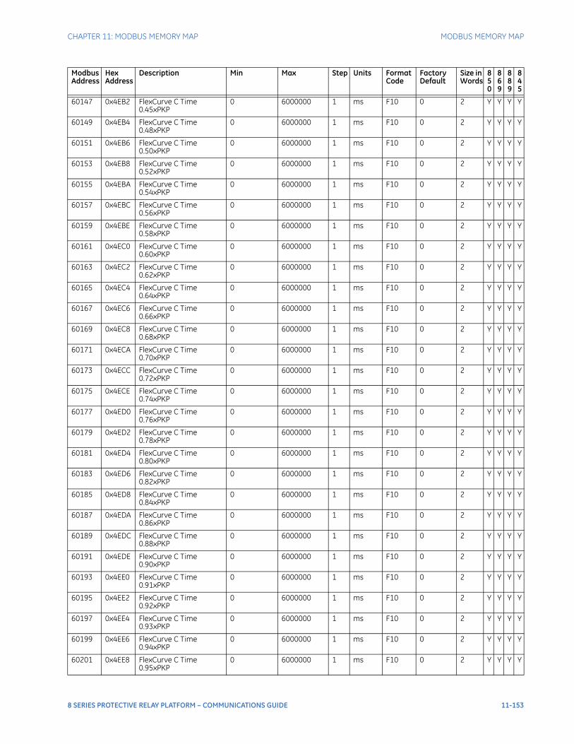
CHAPTER 11: MODBUS MEMORY MAP MODBUS MEMORY MAP
60147 0x4EB2 FlexCurve C Time 0.45xPKP
0 6000000 1 ms F10 0 2 Y Y Y Y
60149 0x4EB4 FlexCurve C Time 0.48xPKP
0 6000000 1 ms F10 0 2 Y Y Y Y
60151 0x4EB6 FlexCurve C Time 0.50xPKP
0 6000000 1 ms F10 0 2 Y Y Y Y
60153 0x4EB8 FlexCurve C Time 0.52xPKP
0 6000000 1 ms F10 0 2 Y Y Y Y
60155 0x4EBA FlexCurve C Time 0.54xPKP
0 6000000 1 ms F10 0 2 Y Y Y Y
60157 0x4EBC FlexCurve C Time 0.56xPKP
0 6000000 1 ms F10 0 2 Y Y Y Y
60159 0x4EBE FlexCurve C Time 0.58xPKP
0 6000000 1 ms F10 0 2 Y Y Y Y
60161 0x4EC0 FlexCurve C Time 0.60xPKP
0 6000000 1 ms F10 0 2 Y Y Y Y
60163 0x4EC2 FlexCurve C Time 0.62xPKP
0 6000000 1 ms F10 0 2 Y Y Y Y
60165 0x4EC4 FlexCurve C Time 0.64xPKP
0 6000000 1 ms F10 0 2 Y Y Y Y
60167 0x4EC6 FlexCurve C Time 0.66xPKP
0 6000000 1 ms F10 0 2 Y Y Y Y
60169 0x4EC8 FlexCurve C Time 0.68xPKP
0 6000000 1 ms F10 0 2 Y Y Y Y
60171 0x4ECA FlexCurve C Time 0.70xPKP
0 6000000 1 ms F10 0 2 Y Y Y Y
60173 0x4ECC FlexCurve C Time 0.72xPKP
0 6000000 1 ms F10 0 2 Y Y Y Y
60175 0x4ECE FlexCurve C Time 0.74xPKP
0 6000000 1 ms F10 0 2 Y Y Y Y
60177 0x4ED0 FlexCurve C Time 0.76xPKP
0 6000000 1 ms F10 0 2 Y Y Y Y
60179 0x4ED2 FlexCurve C Time 0.78xPKP
0 6000000 1 ms F10 0 2 Y Y Y Y
60181 0x4ED4 FlexCurve C Time 0.80xPKP
0 6000000 1 ms F10 0 2 Y Y Y Y
60183 0x4ED6 FlexCurve C Time 0.82xPKP
0 6000000 1 ms F10 0 2 Y Y Y Y
60185 0x4ED8 FlexCurve C Time 0.84xPKP
0 6000000 1 ms F10 0 2 Y Y Y Y
60187 0x4EDA FlexCurve C Time 0.86xPKP
0 6000000 1 ms F10 0 2 Y Y Y Y
60189 0x4EDC FlexCurve C Time 0.88xPKP
0 6000000 1 ms F10 0 2 Y Y Y Y
60191 0x4EDE FlexCurve C Time 0.90xPKP
0 6000000 1 ms F10 0 2 Y Y Y Y
60193 0x4EE0 FlexCurve C Time 0.91xPKP
0 6000000 1 ms F10 0 2 Y Y Y Y
60195 0x4EE2 FlexCurve C Time 0.92xPKP
0 6000000 1 ms F10 0 2 Y Y Y Y
60197 0x4EE4 FlexCurve C Time 0.93xPKP
0 6000000 1 ms F10 0 2 Y Y Y Y
60199 0x4EE6 FlexCurve C Time 0.94xPKP
0 6000000 1 ms F10 0 2 Y Y Y Y
60201 0x4EE8 FlexCurve C Time 0.95xPKP
0 6000000 1 ms F10 0 2 Y Y Y Y
Modbus Address
Hex Address
Description Min Max Step Units Format Code
Factory Default
Size in Words
850
869
889
845
8 SERIES PROTECTIVE RELAY PLATFORM – COMMUNICATIONS GUIDE 11-153
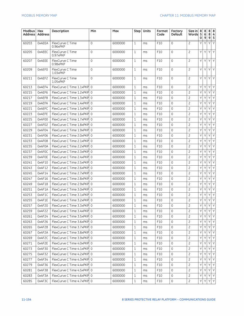
MODBUS MEMORY MAP CHAPTER 11: MODBUS MEMORY MAP
60203 0x4EEA FlexCurve C Time 0.96xPKP
0 6000000 1 ms F10 0 2 Y Y Y Y
60205 0x4EEC FlexCurve C Time 0.97xPKP
0 6000000 1 ms F10 0 2 Y Y Y Y
60207 0x4EEE FlexCurve C Time 0.98xPKP
0 6000000 1 ms F10 0 2 Y Y Y Y
60209 0x4EF0 FlexCurve C Time 1.03xPKP
0 6000000 1 ms F10 0 2 Y Y Y Y
60211 0x4EF2 FlexCurve C Time 1.05xPKP
0 6000000 1 ms F10 0 2 Y Y Y Y
60213 0x4EF4 FlexCurve C Time 1.1xPKP 0 6000000 1 ms F10 0 2 Y Y Y Y
60215 0x4EF6 FlexCurve C Time 1.2xPKP 0 6000000 1 ms F10 0 2 Y Y Y Y
60217 0x4EF8 FlexCurve C Time 1.3xPKP 0 6000000 1 ms F10 0 2 Y Y Y Y
60219 0x4EFA FlexCurve C Time 1.4xPKP 0 6000000 1 ms F10 0 2 Y Y Y Y
60221 0x4EFC FlexCurve C Time 1.5xPKP 0 6000000 1 ms F10 0 2 Y Y Y Y
60223 0x4EFE FlexCurve C Time 1.6xPKP 0 6000000 1 ms F10 0 2 Y Y Y Y
60225 0x4F00 FlexCurve C Time 1.7xPKP 0 6000000 1 ms F10 0 2 Y Y Y Y
60227 0x4F02 FlexCurve C Time 1.8xPKP 0 6000000 1 ms F10 0 2 Y Y Y Y
60229 0x4F04 FlexCurve C Time 1.9xPKP 0 6000000 1 ms F10 0 2 Y Y Y Y
60231 0x4F06 FlexCurve C Time 2.0xPKP 0 6000000 1 ms F10 0 2 Y Y Y Y
60233 0x4F08 FlexCurve C Time 2.1xPKP 0 6000000 1 ms F10 0 2 Y Y Y Y
60235 0x4F0A FlexCurve C Time 2.2xPKP 0 6000000 1 ms F10 0 2 Y Y Y Y
60237 0x4F0C FlexCurve C Time 2.3xPKP 0 6000000 1 ms F10 0 2 Y Y Y Y
60239 0x4F0E FlexCurve C Time 2.4xPKP 0 6000000 1 ms F10 0 2 Y Y Y Y
60241 0x4F10 FlexCurve C Time 2.5xPKP 0 6000000 1 ms F10 0 2 Y Y Y Y
60243 0x4F12 FlexCurve C Time 2.6xPKP 0 6000000 1 ms F10 0 2 Y Y Y Y
60245 0x4F14 FlexCurve C Time 2.7xPKP 0 6000000 1 ms F10 0 2 Y Y Y Y
60247 0x4F16 FlexCurve C Time 2.8xPKP 0 6000000 1 ms F10 0 2 Y Y Y Y
60249 0x4F18 FlexCurve C Time 2.9xPKP 0 6000000 1 ms F10 0 2 Y Y Y Y
60251 0x4F1A FlexCurve C Time 3.0xPKP 0 6000000 1 ms F10 0 2 Y Y Y Y
60253 0x4F1C FlexCurve C Time 3.1xPKP 0 6000000 1 ms F10 0 2 Y Y Y Y
60255 0x4F1E FlexCurve C Time 3.2xPKP 0 6000000 1 ms F10 0 2 Y Y Y Y
60257 0x4F20 FlexCurve C Time 3.3xPKP 0 6000000 1 ms F10 0 2 Y Y Y Y
60259 0x4F22 FlexCurve C Time 3.4xPKP 0 6000000 1 ms F10 0 2 Y Y Y Y
60261 0x4F24 FlexCurve C Time 3.5xPKP 0 6000000 1 ms F10 0 2 Y Y Y Y
60263 0x4F26 FlexCurve C Time 3.6xPKP 0 6000000 1 ms F10 0 2 Y Y Y Y
60265 0x4F28 FlexCurve C Time 3.7xPKP 0 6000000 1 ms F10 0 2 Y Y Y Y
60267 0x4F2A FlexCurve C Time 3.8xPKP 0 6000000 1 ms F10 0 2 Y Y Y Y
60269 0x4F2C FlexCurve C Time 3.9xPKP 0 6000000 1 ms F10 0 2 Y Y Y Y
60271 0x4F2E FlexCurve C Time 4.0xPKP 0 6000000 1 ms F10 0 2 Y Y Y Y
60273 0x4F30 FlexCurve C Time 4.1xPKP 0 6000000 1 ms F10 0 2 Y Y Y Y
60275 0x4F32 FlexCurve C Time 4.2xPKP 0 6000000 1 ms F10 0 2 Y Y Y Y
60277 0x4F34 FlexCurve C Time 4.3xPKP 0 6000000 1 ms F10 0 2 Y Y Y Y
60279 0x4F36 FlexCurve C Time 4.4xPKP 0 6000000 1 ms F10 0 2 Y Y Y Y
60281 0x4F38 FlexCurve C Time 4.5xPKP 0 6000000 1 ms F10 0 2 Y Y Y Y
60283 0x4F3A FlexCurve C Time 4.6xPKP 0 6000000 1 ms F10 0 2 Y Y Y Y
60285 0x4F3C FlexCurve C Time 4.7xPKP 0 6000000 1 ms F10 0 2 Y Y Y Y
Modbus Address
Hex Address
Description Min Max Step Units Format Code
Factory Default
Size in Words
850
869
889
845
11-154 8 SERIES PROTECTIVE RELAY PLATFORM – COMMUNICATIONS GUIDE
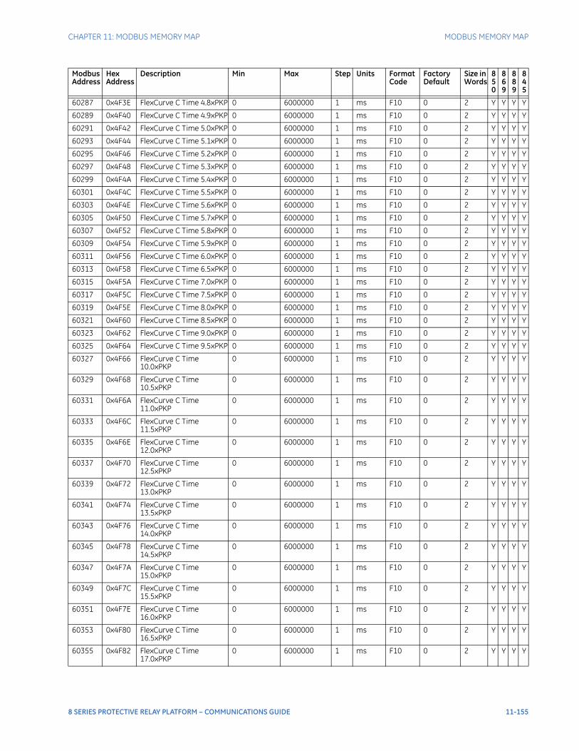
CHAPTER 11: MODBUS MEMORY MAP MODBUS MEMORY MAP
60287 0x4F3E FlexCurve C Time 4.8xPKP 0 6000000 1 ms F10 0 2 Y Y Y Y
60289 0x4F40 FlexCurve C Time 4.9xPKP 0 6000000 1 ms F10 0 2 Y Y Y Y
60291 0x4F42 FlexCurve C Time 5.0xPKP 0 6000000 1 ms F10 0 2 Y Y Y Y
60293 0x4F44 FlexCurve C Time 5.1xPKP 0 6000000 1 ms F10 0 2 Y Y Y Y
60295 0x4F46 FlexCurve C Time 5.2xPKP 0 6000000 1 ms F10 0 2 Y Y Y Y
60297 0x4F48 FlexCurve C Time 5.3xPKP 0 6000000 1 ms F10 0 2 Y Y Y Y
60299 0x4F4A FlexCurve C Time 5.4xPKP 0 6000000 1 ms F10 0 2 Y Y Y Y
60301 0x4F4C FlexCurve C Time 5.5xPKP 0 6000000 1 ms F10 0 2 Y Y Y Y
60303 0x4F4E FlexCurve C Time 5.6xPKP 0 6000000 1 ms F10 0 2 Y Y Y Y
60305 0x4F50 FlexCurve C Time 5.7xPKP 0 6000000 1 ms F10 0 2 Y Y Y Y
60307 0x4F52 FlexCurve C Time 5.8xPKP 0 6000000 1 ms F10 0 2 Y Y Y Y
60309 0x4F54 FlexCurve C Time 5.9xPKP 0 6000000 1 ms F10 0 2 Y Y Y Y
60311 0x4F56 FlexCurve C Time 6.0xPKP 0 6000000 1 ms F10 0 2 Y Y Y Y
60313 0x4F58 FlexCurve C Time 6.5xPKP 0 6000000 1 ms F10 0 2 Y Y Y Y
60315 0x4F5A FlexCurve C Time 7.0xPKP 0 6000000 1 ms F10 0 2 Y Y Y Y
60317 0x4F5C FlexCurve C Time 7.5xPKP 0 6000000 1 ms F10 0 2 Y Y Y Y
60319 0x4F5E FlexCurve C Time 8.0xPKP 0 6000000 1 ms F10 0 2 Y Y Y Y
60321 0x4F60 FlexCurve C Time 8.5xPKP 0 6000000 1 ms F10 0 2 Y Y Y Y
60323 0x4F62 FlexCurve C Time 9.0xPKP 0 6000000 1 ms F10 0 2 Y Y Y Y
60325 0x4F64 FlexCurve C Time 9.5xPKP 0 6000000 1 ms F10 0 2 Y Y Y Y
60327 0x4F66 FlexCurve C Time 10.0xPKP
0 6000000 1 ms F10 0 2 Y Y Y Y
60329 0x4F68 FlexCurve C Time 10.5xPKP
0 6000000 1 ms F10 0 2 Y Y Y Y
60331 0x4F6A FlexCurve C Time 11.0xPKP
0 6000000 1 ms F10 0 2 Y Y Y Y
60333 0x4F6C FlexCurve C Time 11.5xPKP
0 6000000 1 ms F10 0 2 Y Y Y Y
60335 0x4F6E FlexCurve C Time 12.0xPKP
0 6000000 1 ms F10 0 2 Y Y Y Y
60337 0x4F70 FlexCurve C Time 12.5xPKP
0 6000000 1 ms F10 0 2 Y Y Y Y
60339 0x4F72 FlexCurve C Time 13.0xPKP
0 6000000 1 ms F10 0 2 Y Y Y Y
60341 0x4F74 FlexCurve C Time 13.5xPKP
0 6000000 1 ms F10 0 2 Y Y Y Y
60343 0x4F76 FlexCurve C Time 14.0xPKP
0 6000000 1 ms F10 0 2 Y Y Y Y
60345 0x4F78 FlexCurve C Time 14.5xPKP
0 6000000 1 ms F10 0 2 Y Y Y Y
60347 0x4F7A FlexCurve C Time 15.0xPKP
0 6000000 1 ms F10 0 2 Y Y Y Y
60349 0x4F7C FlexCurve C Time 15.5xPKP
0 6000000 1 ms F10 0 2 Y Y Y Y
60351 0x4F7E FlexCurve C Time 16.0xPKP
0 6000000 1 ms F10 0 2 Y Y Y Y
60353 0x4F80 FlexCurve C Time 16.5xPKP
0 6000000 1 ms F10 0 2 Y Y Y Y
60355 0x4F82 FlexCurve C Time 17.0xPKP
0 6000000 1 ms F10 0 2 Y Y Y Y
Modbus Address
Hex Address
Description Min Max Step Units Format Code
Factory Default
Size in Words
850
869
889
845
8 SERIES PROTECTIVE RELAY PLATFORM – COMMUNICATIONS GUIDE 11-155
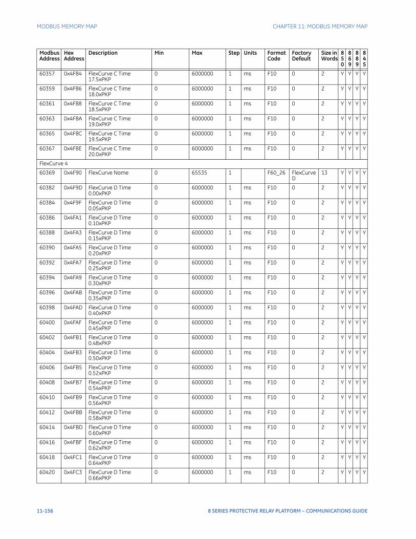
MODBUS MEMORY MAP CHAPTER 11: MODBUS MEMORY MAP
60357 0x4F84 FlexCurve C Time 17.5xPKP
0 6000000 1 ms F10 0 2 Y Y Y Y
60359 0x4F86 FlexCurve C Time 18.0xPKP
0 6000000 1 ms F10 0 2 Y Y Y Y
60361 0x4F88 FlexCurve C Time 18.5xPKP
0 6000000 1 ms F10 0 2 Y Y Y Y
60363 0x4F8A FlexCurve C Time 19.0xPKP
0 6000000 1 ms F10 0 2 Y Y Y Y
60365 0x4F8C FlexCurve C Time 19.5xPKP
0 6000000 1 ms F10 0 2 Y Y Y Y
60367 0x4F8E FlexCurve C Time 20.0xPKP
0 6000000 1 ms F10 0 2 Y Y Y Y
FlexCurve 4
60369 0x4F90 FlexCurve Name 0 65535 1 F60_26 FlexCurve D
13 Y Y Y Y
60382 0x4F9D FlexCurve D Time 0.00xPKP
0 6000000 1 ms F10 0 2 Y Y Y Y
60384 0x4F9F FlexCurve D Time 0.05xPKP
0 6000000 1 ms F10 0 2 Y Y Y Y
60386 0x4FA1 FlexCurve D Time 0.10xPKP
0 6000000 1 ms F10 0 2 Y Y Y Y
60388 0x4FA3 FlexCurve D Time 0.15xPKP
0 6000000 1 ms F10 0 2 Y Y Y Y
60390 0x4FA5 FlexCurve D Time 0.20xPKP
0 6000000 1 ms F10 0 2 Y Y Y Y
60392 0x4FA7 FlexCurve D Time 0.25xPKP
0 6000000 1 ms F10 0 2 Y Y Y Y
60394 0x4FA9 FlexCurve D Time 0.30xPKP
0 6000000 1 ms F10 0 2 Y Y Y Y
60396 0x4FAB FlexCurve D Time 0.35xPKP
0 6000000 1 ms F10 0 2 Y Y Y Y
60398 0x4FAD FlexCurve D Time 0.40xPKP
0 6000000 1 ms F10 0 2 Y Y Y Y
60400 0x4FAF FlexCurve D Time 0.45xPKP
0 6000000 1 ms F10 0 2 Y Y Y Y
60402 0x4FB1 FlexCurve D Time 0.48xPKP
0 6000000 1 ms F10 0 2 Y Y Y Y
60404 0x4FB3 FlexCurve D Time 0.50xPKP
0 6000000 1 ms F10 0 2 Y Y Y Y
60406 0x4FB5 FlexCurve D Time 0.52xPKP
0 6000000 1 ms F10 0 2 Y Y Y Y
60408 0x4FB7 FlexCurve D Time 0.54xPKP
0 6000000 1 ms F10 0 2 Y Y Y Y
60410 0x4FB9 FlexCurve D Time 0.56xPKP
0 6000000 1 ms F10 0 2 Y Y Y Y
60412 0x4FBB FlexCurve D Time 0.58xPKP
0 6000000 1 ms F10 0 2 Y Y Y Y
60414 0x4FBD FlexCurve D Time 0.60xPKP
0 6000000 1 ms F10 0 2 Y Y Y Y
60416 0x4FBF FlexCurve D Time 0.62xPKP
0 6000000 1 ms F10 0 2 Y Y Y Y
60418 0x4FC1 FlexCurve D Time 0.64xPKP
0 6000000 1 ms F10 0 2 Y Y Y Y
60420 0x4FC3 FlexCurve D Time 0.66xPKP
0 6000000 1 ms F10 0 2 Y Y Y Y
Modbus Address
Hex Address
Description Min Max Step Units Format Code
Factory Default
Size in Words
850
869
889
845
11-156 8 SERIES PROTECTIVE RELAY PLATFORM – COMMUNICATIONS GUIDE
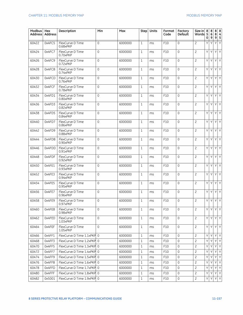
CHAPTER 11: MODBUS MEMORY MAP MODBUS MEMORY MAP
60422 0x4FC5 FlexCurve D Time 0.68xPKP
0 6000000 1 ms F10 0 2 Y Y Y Y
60424 0x4FC7 FlexCurve D Time 0.70xPKP
0 6000000 1 ms F10 0 2 Y Y Y Y
60426 0x4FC9 FlexCurve D Time 0.72xPKP
0 6000000 1 ms F10 0 2 Y Y Y Y
60428 0x4FCB FlexCurve D Time 0.74xPKP
0 6000000 1 ms F10 0 2 Y Y Y Y
60430 0x4FCD FlexCurve D Time 0.76xPKP
0 6000000 1 ms F10 0 2 Y Y Y Y
60432 0x4FCF FlexCurve D Time 0.78xPKP
0 6000000 1 ms F10 0 2 Y Y Y Y
60434 0x4FD1 FlexCurve D Time 0.80xPKP
0 6000000 1 ms F10 0 2 Y Y Y Y
60436 0x4FD3 FlexCurve D Time 0.82xPKP
0 6000000 1 ms F10 0 2 Y Y Y Y
60438 0x4FD5 FlexCurve D Time 0.84xPKP
0 6000000 1 ms F10 0 2 Y Y Y Y
60440 0x4FD7 FlexCurve D Time 0.86xPKP
0 6000000 1 ms F10 0 2 Y Y Y Y
60442 0x4FD9 FlexCurve D Time 0.88xPKP
0 6000000 1 ms F10 0 2 Y Y Y Y
60444 0x4FDB FlexCurve D Time 0.90xPKP
0 6000000 1 ms F10 0 2 Y Y Y Y
60446 0x4FDD FlexCurve D Time 0.91xPKP
0 6000000 1 ms F10 0 2 Y Y Y Y
60448 0x4FDF FlexCurve D Time 0.92xPKP
0 6000000 1 ms F10 0 2 Y Y Y Y
60450 0x4FE1 FlexCurve D Time 0.93xPKP
0 6000000 1 ms F10 0 2 Y Y Y Y
60452 0x4FE3 FlexCurve D Time 0.94xPKP
0 6000000 1 ms F10 0 2 Y Y Y Y
60454 0x4FE5 FlexCurve D Time 0.95xPKP
0 6000000 1 ms F10 0 2 Y Y Y Y
60456 0x4FE7 FlexCurve D Time 0.96xPKP
0 6000000 1 ms F10 0 2 Y Y Y Y
60458 0x4FE9 FlexCurve D Time 0.97xPKP
0 6000000 1 ms F10 0 2 Y Y Y Y
60460 0x4FEB FlexCurve D Time 0.98xPKP
0 6000000 1 ms F10 0 2 Y Y Y Y
60462 0x4FED FlexCurve D Time 1.03xPKP
0 6000000 1 ms F10 0 2 Y Y Y Y
60464 0x4FEF FlexCurve D Time 1.05xPKP
0 6000000 1 ms F10 0 2 Y Y Y Y
60466 0x4FF1 FlexCurve D Time 1.1xPKP 0 6000000 1 ms F10 0 2 Y Y Y Y
60468 0x4FF3 FlexCurve D Time 1.2xPKP 0 6000000 1 ms F10 0 2 Y Y Y Y
60470 0x4FF5 FlexCurve D Time 1.3xPKP 0 6000000 1 ms F10 0 2 Y Y Y Y
60472 0x4FF7 FlexCurve D Time 1.4xPKP 0 6000000 1 ms F10 0 2 Y Y Y Y
60474 0x4FF9 FlexCurve D Time 1.5xPKP 0 6000000 1 ms F10 0 2 Y Y Y Y
60476 0x4FFB FlexCurve D Time 1.6xPKP 0 6000000 1 ms F10 0 2 Y Y Y Y
60478 0x4FFD FlexCurve D Time 1.7xPKP 0 6000000 1 ms F10 0 2 Y Y Y Y
60480 0x4FFF FlexCurve D Time 1.8xPKP 0 6000000 1 ms F10 0 2 Y Y Y Y
60482 0x5001 FlexCurve D Time 1.9xPKP 0 6000000 1 ms F10 0 2 Y Y Y Y
Modbus Address
Hex Address
Description Min Max Step Units Format Code
Factory Default
Size in Words
850
869
889
845
8 SERIES PROTECTIVE RELAY PLATFORM – COMMUNICATIONS GUIDE 11-157
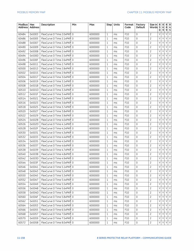
MODBUS MEMORY MAP CHAPTER 11: MODBUS MEMORY MAP
60484 0x5003 FlexCurve D Time 2.0xPKP 0 6000000 1 ms F10 0 2 Y Y Y Y
60486 0x5005 FlexCurve D Time 2.1xPKP 0 6000000 1 ms F10 0 2 Y Y Y Y
60488 0x5007 FlexCurve D Time 2.2xPKP 0 6000000 1 ms F10 0 2 Y Y Y Y
60490 0x5009 FlexCurve D Time 2.3xPKP 0 6000000 1 ms F10 0 2 Y Y Y Y
60492 0x500B FlexCurve D Time 2.4xPKP 0 6000000 1 ms F10 0 2 Y Y Y Y
60494 0x500D FlexCurve D Time 2.5xPKP 0 6000000 1 ms F10 0 2 Y Y Y Y
60496 0x500F FlexCurve D Time 2.6xPKP 0 6000000 1 ms F10 0 2 Y Y Y Y
60498 0x5011 FlexCurve D Time 2.7xPKP 0 6000000 1 ms F10 0 2 Y Y Y Y
60500 0x5013 FlexCurve D Time 2.8xPKP 0 6000000 1 ms F10 0 2 Y Y Y Y
60502 0x5015 FlexCurve D Time 2.9xPKP 0 6000000 1 ms F10 0 2 Y Y Y Y
60504 0x5017 FlexCurve D Time 3.0xPKP 0 6000000 1 ms F10 0 2 Y Y Y Y
60506 0x5019 FlexCurve D Time 3.1xPKP 0 6000000 1 ms F10 0 2 Y Y Y Y
60508 0x501B FlexCurve D Time 3.2xPKP 0 6000000 1 ms F10 0 2 Y Y Y Y
60510 0x501D FlexCurve D Time 3.3xPKP 0 6000000 1 ms F10 0 2 Y Y Y Y
60512 0x501F FlexCurve D Time 3.4xPKP 0 6000000 1 ms F10 0 2 Y Y Y Y
60514 0x5021 FlexCurve D Time 3.5xPKP 0 6000000 1 ms F10 0 2 Y Y Y Y
60516 0x5023 FlexCurve D Time 3.6xPKP 0 6000000 1 ms F10 0 2 Y Y Y Y
60518 0x5025 FlexCurve D Time 3.7xPKP 0 6000000 1 ms F10 0 2 Y Y Y Y
60520 0x5027 FlexCurve D Time 3.8xPKP 0 6000000 1 ms F10 0 2 Y Y Y Y
60522 0x5029 FlexCurve D Time 3.9xPKP 0 6000000 1 ms F10 0 2 Y Y Y Y
60524 0x502B FlexCurve D Time 4.0xPKP 0 6000000 1 ms F10 0 2 Y Y Y Y
60526 0x502D FlexCurve D Time 4.1xPKP 0 6000000 1 ms F10 0 2 Y Y Y Y
60528 0x502F FlexCurve D Time 4.2xPKP 0 6000000 1 ms F10 0 2 Y Y Y Y
60530 0x5031 FlexCurve D Time 4.3xPKP 0 6000000 1 ms F10 0 2 Y Y Y Y
60532 0x5033 FlexCurve D Time 4.4xPKP 0 6000000 1 ms F10 0 2 Y Y Y Y
60534 0x5035 FlexCurve D Time 4.5xPKP 0 6000000 1 ms F10 0 2 Y Y Y Y
60536 0x5037 FlexCurve D Time 4.6xPKP 0 6000000 1 ms F10 0 2 Y Y Y Y
60538 0x5039 FlexCurve D Time 4.7xPKP 0 6000000 1 ms F10 0 2 Y Y Y Y
60540 0x503B FlexCurve D Time 4.8xPKP 0 6000000 1 ms F10 0 2 Y Y Y Y
60542 0x503D FlexCurve D Time 4.9xPKP 0 6000000 1 ms F10 0 2 Y Y Y Y
60544 0x503F FlexCurve D Time 5.0xPKP 0 6000000 1 ms F10 0 2 Y Y Y Y
60546 0x5041 FlexCurve D Time 5.1xPKP 0 6000000 1 ms F10 0 2 Y Y Y Y
60548 0x5043 FlexCurve D Time 5.2xPKP 0 6000000 1 ms F10 0 2 Y Y Y Y
60550 0x5045 FlexCurve D Time 5.3xPKP 0 6000000 1 ms F10 0 2 Y Y Y Y
60552 0x5047 FlexCurve D Time 5.4xPKP 0 6000000 1 ms F10 0 2 Y Y Y Y
60554 0x5049 FlexCurve D Time 5.5xPKP 0 6000000 1 ms F10 0 2 Y Y Y Y
60556 0x504B FlexCurve D Time 5.6xPKP 0 6000000 1 ms F10 0 2 Y Y Y Y
60558 0x504D FlexCurve D Time 5.7xPKP 0 6000000 1 ms F10 0 2 Y Y Y Y
60560 0x504F FlexCurve D Time 5.8xPKP 0 6000000 1 ms F10 0 2 Y Y Y Y
60562 0x5051 FlexCurve D Time 5.9xPKP 0 6000000 1 ms F10 0 2 Y Y Y Y
60564 0x5053 FlexCurve D Time 6.0xPKP 0 6000000 1 ms F10 0 2 Y Y Y Y
60566 0x5055 FlexCurve D Time 6.5xPKP 0 6000000 1 ms F10 0 2 Y Y Y Y
60568 0x5057 FlexCurve D Time 7.0xPKP 0 6000000 1 ms F10 0 2 Y Y Y Y
60570 0x5059 FlexCurve D Time 7.5xPKP 0 6000000 1 ms F10 0 2 Y Y Y Y
60572 0x505B FlexCurve D Time 8.0xPKP 0 6000000 1 ms F10 0 2 Y Y Y Y
Modbus Address
Hex Address
Description Min Max Step Units Format Code
Factory Default
Size in Words
850
869
889
845
11-158 8 SERIES PROTECTIVE RELAY PLATFORM – COMMUNICATIONS GUIDE
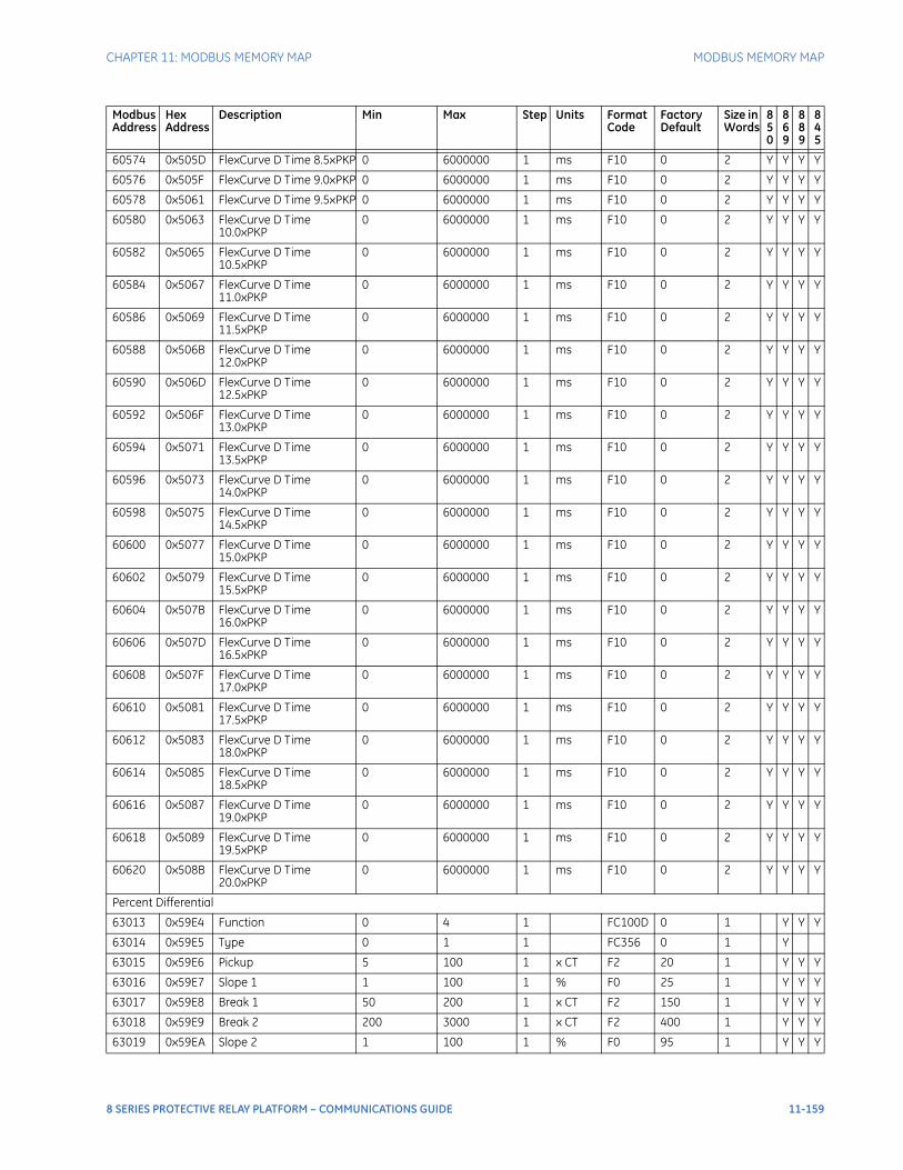
CHAPTER 11: MODBUS MEMORY MAP MODBUS MEMORY MAP
60574 0x505D FlexCurve D Time 8.5xPKP 0 6000000 1 ms F10 0 2 Y Y Y Y
60576 0x505F FlexCurve D Time 9.0xPKP 0 6000000 1 ms F10 0 2 Y Y Y Y
60578 0x5061 FlexCurve D Time 9.5xPKP 0 6000000 1 ms F10 0 2 Y Y Y Y
60580 0x5063 FlexCurve D Time 10.0xPKP
0 6000000 1 ms F10 0 2 Y Y Y Y
60582 0x5065 FlexCurve D Time 10.5xPKP
0 6000000 1 ms F10 0 2 Y Y Y Y
60584 0x5067 FlexCurve D Time 11.0xPKP
0 6000000 1 ms F10 0 2 Y Y Y Y
60586 0x5069 FlexCurve D Time 11.5xPKP
0 6000000 1 ms F10 0 2 Y Y Y Y
60588 0x506B FlexCurve D Time 12.0xPKP
0 6000000 1 ms F10 0 2 Y Y Y Y
60590 0x506D FlexCurve D Time 12.5xPKP
0 6000000 1 ms F10 0 2 Y Y Y Y
60592 0x506F FlexCurve D Time 13.0xPKP
0 6000000 1 ms F10 0 2 Y Y Y Y
60594 0x5071 FlexCurve D Time 13.5xPKP
0 6000000 1 ms F10 0 2 Y Y Y Y
60596 0x5073 FlexCurve D Time 14.0xPKP
0 6000000 1 ms F10 0 2 Y Y Y Y
60598 0x5075 FlexCurve D Time 14.5xPKP
0 6000000 1 ms F10 0 2 Y Y Y Y
60600 0x5077 FlexCurve D Time 15.0xPKP
0 6000000 1 ms F10 0 2 Y Y Y Y
60602 0x5079 FlexCurve D Time 15.5xPKP
0 6000000 1 ms F10 0 2 Y Y Y Y
60604 0x507B FlexCurve D Time 16.0xPKP
0 6000000 1 ms F10 0 2 Y Y Y Y
60606 0x507D FlexCurve D Time 16.5xPKP
0 6000000 1 ms F10 0 2 Y Y Y Y
60608 0x507F FlexCurve D Time 17.0xPKP
0 6000000 1 ms F10 0 2 Y Y Y Y
60610 0x5081 FlexCurve D Time 17.5xPKP
0 6000000 1 ms F10 0 2 Y Y Y Y
60612 0x5083 FlexCurve D Time 18.0xPKP
0 6000000 1 ms F10 0 2 Y Y Y Y
60614 0x5085 FlexCurve D Time 18.5xPKP
0 6000000 1 ms F10 0 2 Y Y Y Y
60616 0x5087 FlexCurve D Time 19.0xPKP
0 6000000 1 ms F10 0 2 Y Y Y Y
60618 0x5089 FlexCurve D Time 19.5xPKP
0 6000000 1 ms F10 0 2 Y Y Y Y
60620 0x508B FlexCurve D Time 20.0xPKP
0 6000000 1 ms F10 0 2 Y Y Y Y
Percent Differential
63013 0x59E4 Function 0 4 1 FC100D 0 1 Y Y Y
63014 0x59E5 Type 0 1 1 FC356 0 1 Y
63015 0x59E6 Pickup 5 100 1 x CT F2 20 1 Y Y Y
63016 0x59E7 Slope 1 1 100 1 % F0 25 1 Y Y Y
63017 0x59E8 Break 1 50 200 1 x CT F2 150 1 Y Y Y
63018 0x59E9 Break 2 200 3000 1 x CT F2 400 1 Y Y Y
63019 0x59EA Slope 2 1 100 1 % F0 95 1 Y Y Y
Modbus Address
Hex Address
Description Min Max Step Units Format Code
Factory Default
Size in Words
850
869
889
845
8 SERIES PROTECTIVE RELAY PLATFORM – COMMUNICATIONS GUIDE 11-159

MODBUS MEMORY MAP CHAPTER 11: MODBUS MEMORY MAP
63020 0x59EB Pickup Delay 0 10000 1 s F3 0 1 Y Y Y
63021 0x59EC Restraint Factor Starting 0 1000 1 F3 100 1 Y
63022 0x59ED Inrush Inhibit 0 1 1 FC357 1 1 Y
63023 0x59EE Inrush Inhibit Level 10 400 1 % F1 200 1 Y
63024 0x59EF Inrush Inhibit Mode 0 3 1 FC358 0 1 Y
63025 0x59F0 Overexcitation Inhibit 0 1 1 FC359 1 1 Y
63026 0x59F1 Overexcitation Level 10 400 1 % F1 100 1 Y
63027 0x59F2 Block 0 0xFFFFFFFF 1 FC142 0 2 Y Y Y
63029 0x59F4 Relays 0 0xFFFFFFFF 1 FC198H 0 2 Y Y Y
63031 0x59F6 Instantaneous Diff Function
0 4 1 FC100 0 1 Y
63032 0x59F7 Inst Diff Pickup 300 3000 1 x CT F2 1000 1 Y
63033 0x59F8 Inst Diff Block 0 0xFFFFFFFF 1 FC142 0 2 Y
63035 0x59FA Inst Diff Output Relays 0 0xFFFFFFFF 1 FC198I 0 2 Y
63037 0x59FC Events 0 1 1 FC126 1 1 Y Y Y
63038 0x59FD Targets 0 2 1 FC101 2 1 Y Y Y
Overall Percent Differential
63065 0x5A18 Function 0 4 1 FC100D 0 1 Y
63067 0x5A1A Pickup 5 100 1 x CT F2 20 1 Y
63068 0x5A1B Slope 1 1 100 1 % F0 25 1 Y
63069 0x5A1C Break 1 50 200 1 x CT F2 150 1 Y
63070 0x5A1D Break 2 200 3000 1 x CT F2 400 1 Y
63071 0x5A1E Slope 2 1 100 1 % F0 95 1 Y
63072 0x5A1F Pickup Delay 0 10000 1 s F3 0 1 Y
63074 0x5A21 Inrush Inhibit 0 1 1 FC357 1 1 Y
63075 0x5A22 Inrush Inhibit Level 10 400 1 % F1 200 1 Y
63076 0x5A23 Inrush Inhibit Mode 0 3 1 FC358 0 1 Y
63077 0x5A24 Overexcitation Inhibit 0 1 1 FC359 1 1 Y
63078 0x5A25 Overexcitation Level 10 400 1 % F1 100 1 Y
63079 0x5A26 Block 0 0xFFFFFFFF 1 FC142 0 2 Y
63081 0x5A28 Relays 0 0xFFFFFFFF 1 FC198H 0 2 Y
63083 0x5A2A Instantaneous Diff Function
0 4 1 FC100 0 1 Y
63084 0x5A2B Inst Diff Pickup 300 3000 1 x CT F2 1000 1 Y
63085 0x5A2C Inst Diff Block 0 0xFFFFFFFF 1 FC142 0 2 Y
63087 0x5A2E Inst Diff Output Relays 0 0xFFFFFFFF 1 FC198I 0 2 Y
63089 0x5A30 Events 0 1 1 FC126 1 1 Y
63090 0x5A31 Targets 0 2 1 FC101 2 1 Y
869 Thermal Model
63123 0x5A52 Trip Function 0 4 1 FC100D 0 1 Y
63125 0x5A54 Overload Curve 16 23 1 FC161C 23 1 Y
63126 0x5A55 Curve Effect 0 1 1 FC353 0 1 Y
63127 0x5A56 Curve k Factor 100 150 5 F2 110 1 Y
63128 0x5A57 IEC Curve Time Constant 0 1000 1 min F0 45 1 Y
63129 0x5A58 TD Multiplier 0 2500 1 F2 100 1 Y
63130 0x5A59 TD Multiplier 0 60000 1 F2 0 1 Y
Modbus Address
Hex Address
Description Min Max Step Units Format Code
Factory Default
Size in Words
850
869
889
845
11-160 8 SERIES PROTECTIVE RELAY PLATFORM – COMMUNICATIONS GUIDE
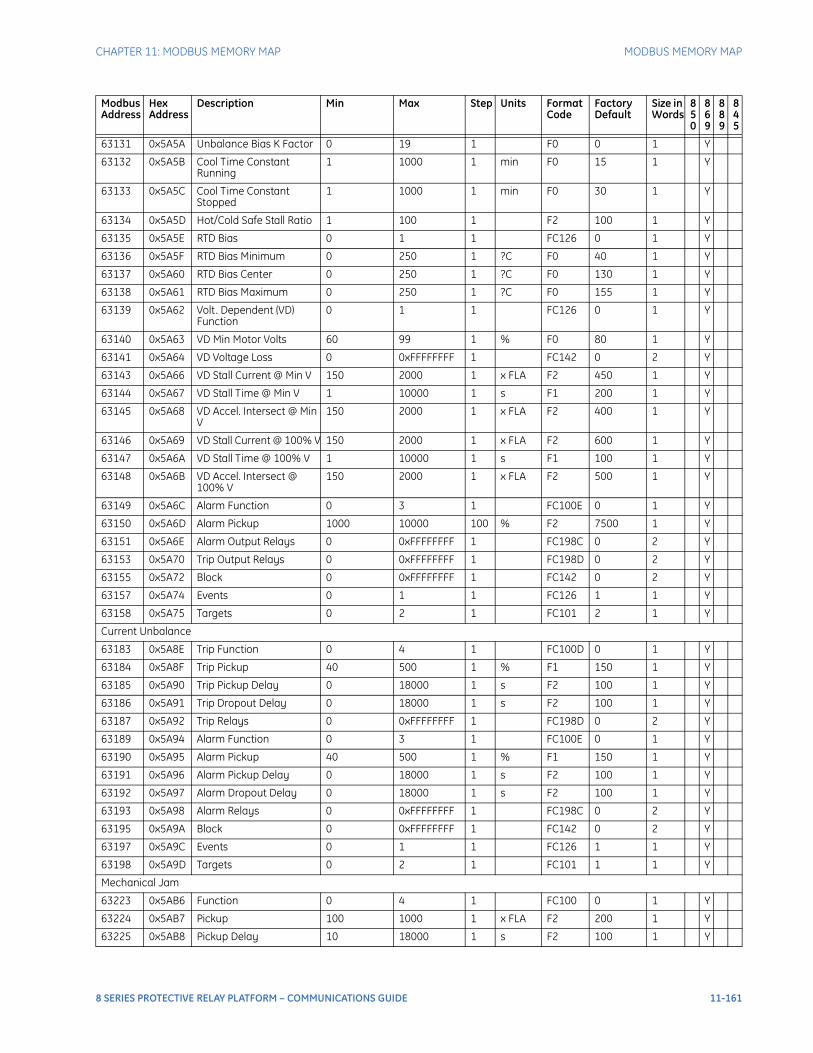
CHAPTER 11: MODBUS MEMORY MAP MODBUS MEMORY MAP
63131 0x5A5A Unbalance Bias K Factor 0 19 1 F0 0 1 Y
63132 0x5A5B Cool Time Constant Running
1 1000 1 min F0 15 1 Y
63133 0x5A5C Cool Time Constant Stopped
1 1000 1 min F0 30 1 Y
63134 0x5A5D Hot/Cold Safe Stall Ratio 1 100 1 F2 100 1 Y
63135 0x5A5E RTD Bias 0 1 1 FC126 0 1 Y
63136 0x5A5F RTD Bias Minimum 0 250 1 ?C F0 40 1 Y
63137 0x5A60 RTD Bias Center 0 250 1 ?C F0 130 1 Y
63138 0x5A61 RTD Bias Maximum 0 250 1 ?C F0 155 1 Y
63139 0x5A62 Volt. Dependent (VD) Function
0 1 1 FC126 0 1 Y
63140 0x5A63 VD Min Motor Volts 60 99 1 % F0 80 1 Y
63141 0x5A64 VD Voltage Loss 0 0xFFFFFFFF 1 FC142 0 2 Y
63143 0x5A66 VD Stall Current @ Min V 150 2000 1 x FLA F2 450 1 Y
63144 0x5A67 VD Stall Time @ Min V 1 10000 1 s F1 200 1 Y
63145 0x5A68 VD Accel. Intersect @ Min V
150 2000 1 x FLA F2 400 1 Y
63146 0x5A69 VD Stall Current @ 100% V 150 2000 1 x FLA F2 600 1 Y
63147 0x5A6A VD Stall Time @ 100% V 1 10000 1 s F1 100 1 Y
63148 0x5A6B VD Accel. Intersect @ 100% V
150 2000 1 x FLA F2 500 1 Y
63149 0x5A6C Alarm Function 0 3 1 FC100E 0 1 Y
63150 0x5A6D Alarm Pickup 1000 10000 100 % F2 7500 1 Y
63151 0x5A6E Alarm Output Relays 0 0xFFFFFFFF 1 FC198C 0 2 Y
63153 0x5A70 Trip Output Relays 0 0xFFFFFFFF 1 FC198D 0 2 Y
63155 0x5A72 Block 0 0xFFFFFFFF 1 FC142 0 2 Y
63157 0x5A74 Events 0 1 1 FC126 1 1 Y
63158 0x5A75 Targets 0 2 1 FC101 2 1 Y
Current Unbalance
63183 0x5A8E Trip Function 0 4 1 FC100D 0 1 Y
63184 0x5A8F Trip Pickup 40 500 1 % F1 150 1 Y
63185 0x5A90 Trip Pickup Delay 0 18000 1 s F2 100 1 Y
63186 0x5A91 Trip Dropout Delay 0 18000 1 s F2 100 1 Y
63187 0x5A92 Trip Relays 0 0xFFFFFFFF 1 FC198D 0 2 Y
63189 0x5A94 Alarm Function 0 3 1 FC100E 0 1 Y
63190 0x5A95 Alarm Pickup 40 500 1 % F1 150 1 Y
63191 0x5A96 Alarm Pickup Delay 0 18000 1 s F2 100 1 Y
63192 0x5A97 Alarm Dropout Delay 0 18000 1 s F2 100 1 Y
63193 0x5A98 Alarm Relays 0 0xFFFFFFFF 1 FC198C 0 2 Y
63195 0x5A9A Block 0 0xFFFFFFFF 1 FC142 0 2 Y
63197 0x5A9C Events 0 1 1 FC126 1 1 Y
63198 0x5A9D Targets 0 2 1 FC101 1 1 Y
Mechanical Jam
63223 0x5AB6 Function 0 4 1 FC100 0 1 Y
63224 0x5AB7 Pickup 100 1000 1 x FLA F2 200 1 Y
63225 0x5AB8 Pickup Delay 10 18000 1 s F2 100 1 Y
Modbus Address
Hex Address
Description Min Max Step Units Format Code
Factory Default
Size in Words
850
869
889
845
8 SERIES PROTECTIVE RELAY PLATFORM – COMMUNICATIONS GUIDE 11-161
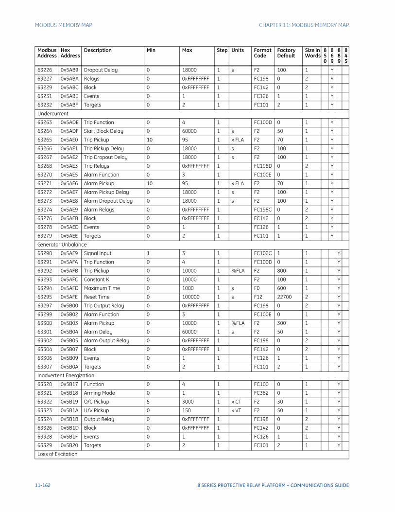
MODBUS MEMORY MAP CHAPTER 11: MODBUS MEMORY MAP
63226 0x5AB9 Dropout Delay 0 18000 1 s F2 100 1 Y
63227 0x5ABA Relays 0 0xFFFFFFFF 1 FC198 0 2 Y
63229 0x5ABC Block 0 0xFFFFFFFF 1 FC142 0 2 Y
63231 0x5ABE Events 0 1 1 FC126 1 1 Y
63232 0x5ABF Targets 0 2 1 FC101 2 1 Y
Undercurrent
63263 0x5ADE Trip Function 0 4 1 FC100D 0 1 Y
63264 0x5ADF Start Block Delay 0 60000 1 s F2 50 1 Y
63265 0x5AE0 Trip Pickup 10 95 1 x FLA F2 70 1 Y
63266 0x5AE1 Trip Pickup Delay 0 18000 1 s F2 100 1 Y
63267 0x5AE2 Trip Dropout Delay 0 18000 1 s F2 100 1 Y
63268 0x5AE3 Trip Relays 0 0xFFFFFFFF 1 FC198D 0 2 Y
63270 0x5AE5 Alarm Function 0 3 1 FC100E 0 1 Y
63271 0x5AE6 Alarm Pickup 10 95 1 x FLA F2 70 1 Y
63272 0x5AE7 Alarm Pickup Delay 0 18000 1 s F2 100 1 Y
63273 0x5AE8 Alarm Dropout Delay 0 18000 1 s F2 100 1 Y
63274 0x5AE9 Alarm Relays 0 0xFFFFFFFF 1 FC198C 0 2 Y
63276 0x5AEB Block 0 0xFFFFFFFF 1 FC142 0 2 Y
63278 0x5AED Events 0 1 1 FC126 1 1 Y
63279 0x5AEE Targets 0 2 1 FC101 1 1 Y
Generator Unbalance
63290 0x5AF9 Signal Input 1 3 1 FC102C 1 1 Y
63291 0x5AFA Trip Function 0 4 1 FC100D 0 1 Y
63292 0x5AFB Trip Pickup 0 10000 1 %FLA F2 800 1 Y
63293 0x5AFC Constant K 0 10000 1 F2 100 1 Y
63294 0x5AFD Maximum Time 0 1000 1 s F0 600 1 Y
63295 0x5AFE Reset Time 0 100000 1 s F12 22700 2 Y
63297 0x5B00 Trip Output Relay 0 0xFFFFFFFF 1 FC198 0 2 Y
63299 0x5B02 Alarm Function 0 3 1 FC100E 0 1 Y
63300 0x5B03 Alarm Pickup 0 10000 1 %FLA F2 300 1 Y
63301 0x5B04 Alarm Delay 0 60000 1 s F2 50 1 Y
63302 0x5B05 Alarm Output Relay 0 0xFFFFFFFF 1 FC198 0 2 Y
63304 0x5B07 Block 0 0xFFFFFFFF 1 FC142 0 2 Y
63306 0x5B09 Events 0 1 1 FC126 1 1 Y
63307 0x5B0A Targets 0 2 1 FC101 2 1 Y
Inadvertent Energization
63320 0x5B17 Function 0 4 1 FC100 0 1 Y
63321 0x5B18 Arming Mode 0 1 1 FC382 0 1 Y
63322 0x5B19 O/C Pickup 5 3000 1 x CT F2 30 1 Y
63323 0x5B1A U/V Pickup 0 150 1 x VT F2 50 1 Y
63324 0x5B1B Output Relay 0 0xFFFFFFFF 1 FC198 0 2 Y
63326 0x5B1D Block 0 0xFFFFFFFF 1 FC142 0 2 Y
63328 0x5B1F Events 0 1 1 FC126 1 1 Y
63329 0x5B20 Targets 0 2 1 FC101 2 1 Y
Loss of Excitation
Modbus Address
Hex Address
Description Min Max Step Units Format Code
Factory Default
Size in Words
850
869
889
845
11-162 8 SERIES PROTECTIVE RELAY PLATFORM – COMMUNICATIONS GUIDE
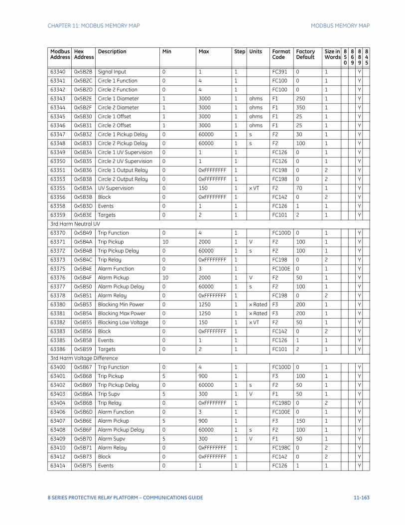
CHAPTER 11: MODBUS MEMORY MAP MODBUS MEMORY MAP
63340 0x5B2B Signal Input 0 1 1 FC391 0 1 Y
63341 0x5B2C Circle 1 Function 0 4 1 FC100 0 1 Y
63342 0x5B2D Circle 2 Function 0 4 1 FC100 0 1 Y
63343 0x5B2E Circle 1 Diameter 1 3000 1 ohms F1 250 1 Y
63344 0x5B2F Circle 2 Diameter 1 3000 1 ohms F1 350 1 Y
63345 0x5B30 Circle 1 Offset 1 3000 1 ohms F1 25 1 Y
63346 0x5B31 Circle 2 Offset 1 3000 1 ohms F1 25 1 Y
63347 0x5B32 Circle 1 Pickup Delay 0 60000 1 s F2 30 1 Y
63348 0x5B33 Circle 2 Pickup Delay 0 60000 1 s F2 100 1 Y
63349 0x5B34 Circle 1 UV Supervision 0 1 1 FC126 0 1 Y
63350 0x5B35 Circle 2 UV Supervision 0 1 1 FC126 0 1 Y
63351 0x5B36 Circle 1 Output Relay 0 0xFFFFFFFF 1 FC198 0 2 Y
63353 0x5B38 Circle 2 Output Relay 0 0xFFFFFFFF 1 FC198 0 2 Y
63355 0x5B3A UV Supervision 0 150 1 x VT F2 70 1 Y
63356 0x5B3B Block 0 0xFFFFFFFF 1 FC142 0 2 Y
63358 0x5B3D Events 0 1 1 FC126 1 1 Y
63359 0x5B3E Targets 0 2 1 FC101 2 1 Y
3rd Harm Neutral UV
63370 0x5B49 Trip Function 0 4 1 FC100D 0 1 Y
63371 0x5B4A Trip Pickup 10 2000 1 V F2 100 1 Y
63372 0x5B4B Trip Pickup Delay 0 60000 1 s F2 100 1 Y
63373 0x5B4C Trip Relay 0 0xFFFFFFFF 1 FC198 0 2 Y
63375 0x5B4E Alarm Function 0 3 1 FC100E 0 1 Y
63376 0x5B4F Alarm Pickup 10 2000 1 V F2 50 1 Y
63377 0x5B50 Alarm Pickup Delay 0 60000 1 s F2 100 1 Y
63378 0x5B51 Alarm Relay 0 0xFFFFFFFF 1 FC198 0 2 Y
63380 0x5B53 Blocking Min Power 0 1250 1 x Rated F3 200 1 Y
63381 0x5B54 Blocking Max Power 0 1250 1 x Rated F3 200 1 Y
63382 0x5B55 Blocking Low Voltage 0 150 1 x VT F2 50 1 Y
63383 0x5B56 Block 0 0xFFFFFFFF 1 FC142 0 2 Y
63385 0x5B58 Events 0 1 1 FC126 1 1 Y
63386 0x5B59 Targets 0 2 1 FC101 2 1 Y
3rd Harm Voltage Difference
63400 0x5B67 Trip Function 0 4 1 FC100D 0 1 Y
63401 0x5B68 Trip Pickup 5 900 1 F3 100 1 Y
63402 0x5B69 Trip Pickup Delay 0 60000 1 s F2 50 1 Y
63403 0x5B6A Trip Supv 5 300 1 V F1 50 1 Y
63404 0x5B6B Trip Relay 0 0xFFFFFFFF 1 FC198D 0 2 Y
63406 0x5B6D Alarm Function 0 3 1 FC100E 0 1 Y
63407 0x5B6E Alarm Pickup 5 900 1 F3 150 1 Y
63408 0x5B6F Alarm Pickup Delay 0 60000 1 s F2 100 1 Y
63409 0x5B70 Alarm Supv 5 300 1 V F1 50 1 Y
63410 0x5B71 Alarm Relay 0 0xFFFFFFFF 1 FC198C 0 2 Y
63412 0x5B73 Block 0 0xFFFFFFFF 1 FC142 0 2 Y
63414 0x5B75 Events 0 1 1 FC126 1 1 Y
Modbus Address
Hex Address
Description Min Max Step Units Format Code
Factory Default
Size in Words
850
869
889
845
8 SERIES PROTECTIVE RELAY PLATFORM – COMMUNICATIONS GUIDE 11-163
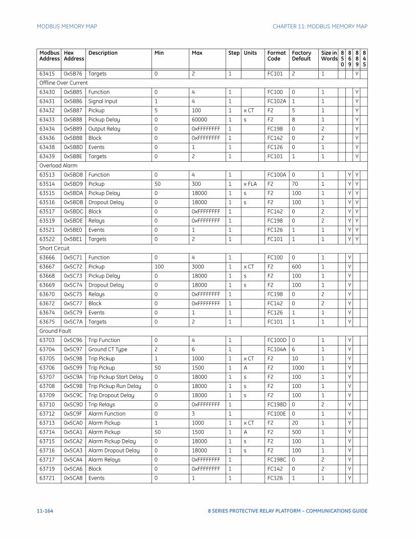
MODBUS MEMORY MAP CHAPTER 11: MODBUS MEMORY MAP
63415 0x5B76 Targets 0 2 1 FC101 2 1 Y
Offline Over Current
63430 0x5B85 Function 0 4 1 FC100 0 1 Y
63431 0x5B86 Signal Input 1 4 1 FC102A 1 1 Y
63432 0x5B87 Pickup 5 100 1 x CT F2 5 1 Y
63433 0x5B88 Pickup Delay 0 60000 1 s F2 8 1 Y
63434 0x5B89 Output Relay 0 0xFFFFFFFF 1 FC198 0 2 Y
63436 0x5B8B Block 0 0xFFFFFFFF 1 FC142 0 2 Y
63438 0x5B8D Events 0 1 1 FC126 0 1 Y
63439 0x5B8E Targets 0 2 1 FC101 1 1 Y
Overload Alarm
63513 0x5BD8 Function 0 4 1 FC100A 0 1 Y Y
63514 0x5BD9 Pickup 50 300 1 x FLA F2 70 1 Y Y
63515 0x5BDA Pickup Delay 0 18000 1 s F2 100 1 Y Y
63516 0x5BDB Dropout Delay 0 18000 1 s F2 100 1 Y Y
63517 0x5BDC Block 0 0xFFFFFFFF 1 FC142 0 2 Y Y
63519 0x5BDE Relays 0 0xFFFFFFFF 1 FC198 0 2 Y Y
63521 0x5BE0 Events 0 1 1 FC126 1 1 Y Y
63522 0x5BE1 Targets 0 2 1 FC101 1 1 Y Y
Short Circuit
63666 0x5C71 Function 0 4 1 FC100 0 1 Y
63667 0x5C72 Pickup 100 3000 1 x CT F2 600 1 Y
63668 0x5C73 Pickup Delay 0 18000 1 s F2 100 1 Y
63669 0x5C74 Dropout Delay 0 18000 1 s F2 100 1 Y
63670 0x5C75 Relays 0 0xFFFFFFFF 1 FC198 0 2 Y
63672 0x5C77 Block 0 0xFFFFFFFF 1 FC142 0 2 Y
63674 0x5C79 Events 0 1 1 FC126 1 1 Y
63675 0x5C7A Targets 0 2 1 FC101 1 1 Y
Ground Fault
63703 0x5C96 Trip Function 0 4 1 FC100D 0 1 Y
63704 0x5C97 Ground CT Type 2 6 1 FC104A 6 1 Y
63705 0x5C98 Trip Pickup 1 1000 1 x CT F2 10 1 Y
63706 0x5C99 Trip Pickup 50 1500 1 A F2 1000 1 Y
63707 0x5C9A Trip Pickup Start Delay 0 18000 1 s F2 100 1 Y
63708 0x5C9B Trip Pickup Run Delay 0 18000 1 s F2 100 1 Y
63709 0x5C9C Trip Dropout Delay 0 18000 1 s F2 100 1 Y
63710 0x5C9D Trip Relays 0 0xFFFFFFFF 1 FC198D 0 2 Y
63712 0x5C9F Alarm Function 0 3 1 FC100E 0 1 Y
63713 0x5CA0 Alarm Pickup 1 1000 1 x CT F2 20 1 Y
63714 0x5CA1 Alarm Pickup 50 1500 1 A F2 500 1 Y
63715 0x5CA2 Alarm Pickup Delay 0 18000 1 s F2 100 1 Y
63716 0x5CA3 Alarm Dropout Delay 0 18000 1 s F2 100 1 Y
63717 0x5CA4 Alarm Relays 0 0xFFFFFFFF 1 FC198C 0 2 Y
63719 0x5CA6 Block 0 0xFFFFFFFF 1 FC142 0 2 Y
63721 0x5CA8 Events 0 1 1 FC126 1 1 Y
Modbus Address
Hex Address
Description Min Max Step Units Format Code
Factory Default
Size in Words
850
869
889
845
11-164 8 SERIES PROTECTIVE RELAY PLATFORM – COMMUNICATIONS GUIDE
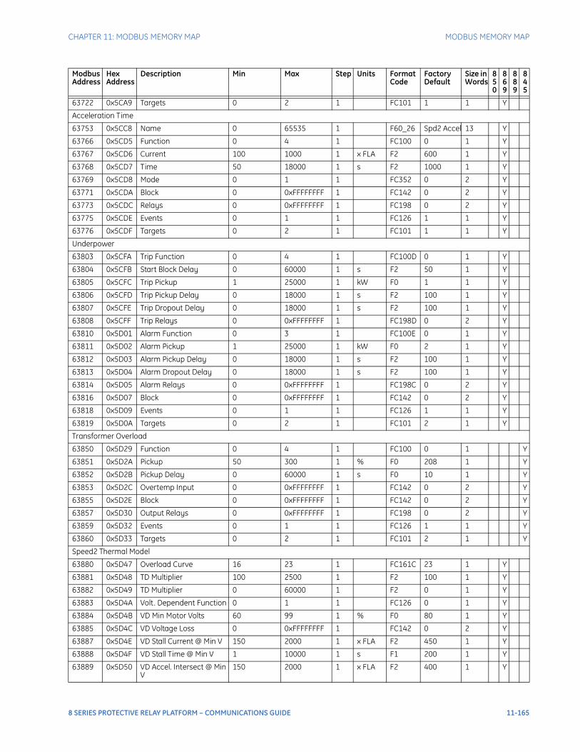
CHAPTER 11: MODBUS MEMORY MAP MODBUS MEMORY MAP
63722 0x5CA9 Targets 0 2 1 FC101 1 1 Y
Acceleration Time
63753 0x5CC8 Name 0 65535 1 F60_26 Spd2 Accel 13 Y
63766 0x5CD5 Function 0 4 1 FC100 0 1 Y
63767 0x5CD6 Current 100 1000 1 x FLA F2 600 1 Y
63768 0x5CD7 Time 50 18000 1 s F2 1000 1 Y
63769 0x5CD8 Mode 0 1 1 FC352 0 2 Y
63771 0x5CDA Block 0 0xFFFFFFFF 1 FC142 0 2 Y
63773 0x5CDC Relays 0 0xFFFFFFFF 1 FC198 0 2 Y
63775 0x5CDE Events 0 1 1 FC126 1 1 Y
63776 0x5CDF Targets 0 2 1 FC101 1 1 Y
Underpower
63803 0x5CFA Trip Function 0 4 1 FC100D 0 1 Y
63804 0x5CFB Start Block Delay 0 60000 1 s F2 50 1 Y
63805 0x5CFC Trip Pickup 1 25000 1 kW F0 1 1 Y
63806 0x5CFD Trip Pickup Delay 0 18000 1 s F2 100 1 Y
63807 0x5CFE Trip Dropout Delay 0 18000 1 s F2 100 1 Y
63808 0x5CFF Trip Relays 0 0xFFFFFFFF 1 FC198D 0 2 Y
63810 0x5D01 Alarm Function 0 3 1 FC100E 0 1 Y
63811 0x5D02 Alarm Pickup 1 25000 1 kW F0 2 1 Y
63812 0x5D03 Alarm Pickup Delay 0 18000 1 s F2 100 1 Y
63813 0x5D04 Alarm Dropout Delay 0 18000 1 s F2 100 1 Y
63814 0x5D05 Alarm Relays 0 0xFFFFFFFF 1 FC198C 0 2 Y
63816 0x5D07 Block 0 0xFFFFFFFF 1 FC142 0 2 Y
63818 0x5D09 Events 0 1 1 FC126 1 1 Y
63819 0x5D0A Targets 0 2 1 FC101 2 1 Y
Transformer Overload
63850 0x5D29 Function 0 4 1 FC100 0 1 Y
63851 0x5D2A Pickup 50 300 1 % F0 208 1 Y
63852 0x5D2B Pickup Delay 0 60000 1 s F0 10 1 Y
63853 0x5D2C Overtemp Input 0 0xFFFFFFFF 1 FC142 0 2 Y
63855 0x5D2E Block 0 0xFFFFFFFF 1 FC142 0 2 Y
63857 0x5D30 Output Relays 0 0xFFFFFFFF 1 FC198 0 2 Y
63859 0x5D32 Events 0 1 1 FC126 1 1 Y
63860 0x5D33 Targets 0 2 1 FC101 2 1 Y
Speed2 Thermal Model
63880 0x5D47 Overload Curve 16 23 1 FC161C 23 1 Y
63881 0x5D48 TD Multiplier 100 2500 1 F2 100 1 Y
63882 0x5D49 TD Multiplier 0 60000 1 F2 0 1 Y
63883 0x5D4A Volt. Dependent Function 0 1 1 FC126 0 1 Y
63884 0x5D4B VD Min Motor Volts 60 99 1 % F0 80 1 Y
63885 0x5D4C VD Voltage Loss 0 0xFFFFFFFF 1 FC142 0 2 Y
63887 0x5D4E VD Stall Current @ Min V 150 2000 1 x FLA F2 450 1 Y
63888 0x5D4F VD Stall Time @ Min V 1 10000 1 s F1 200 1 Y
63889 0x5D50 VD Accel. Intersect @ Min V
150 2000 1 x FLA F2 400 1 Y
Modbus Address
Hex Address
Description Min Max Step Units Format Code
Factory Default
Size in Words
850
869
889
845
8 SERIES PROTECTIVE RELAY PLATFORM – COMMUNICATIONS GUIDE 11-165
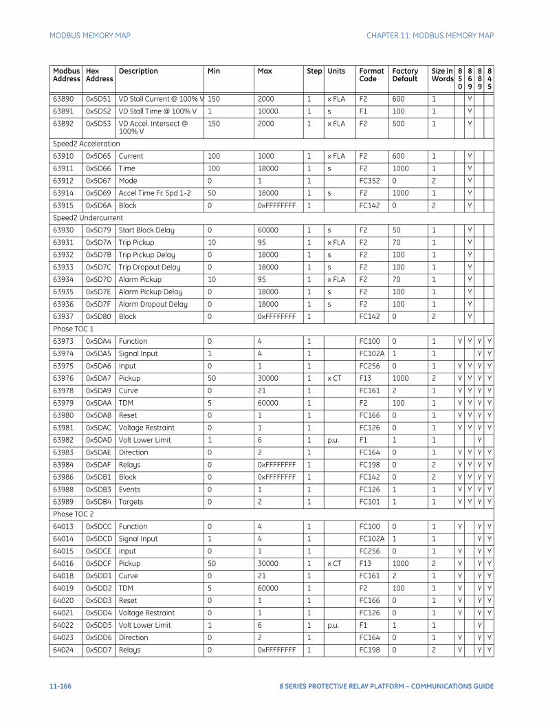
MODBUS MEMORY MAP CHAPTER 11: MODBUS MEMORY MAP
63890 0x5D51 VD Stall Current @ 100% V 150 2000 1 x FLA F2 600 1 Y
63891 0x5D52 VD Stall Time @ 100% V 1 10000 1 s F1 100 1 Y
63892 0x5D53 VD Accel. Intersect @ 100% V
150 2000 1 x FLA F2 500 1 Y
Speed2 Acceleration
63910 0x5D65 Current 100 1000 1 x FLA F2 600 1 Y
63911 0x5D66 Time 100 18000 1 s F2 1000 1 Y
63912 0x5D67 Mode 0 1 1 FC352 0 2 Y
63914 0x5D69 Accel Time Fr. Spd 1-2 50 18000 1 s F2 1000 1 Y
63915 0x5D6A Block 0 0xFFFFFFFF 1 FC142 0 2 Y
Speed2 Undercurrent
63930 0x5D79 Start Block Delay 0 60000 1 s F2 50 1 Y
63931 0x5D7A Trip Pickup 10 95 1 x FLA F2 70 1 Y
63932 0x5D7B Trip Pickup Delay 0 18000 1 s F2 100 1 Y
63933 0x5D7C Trip Dropout Delay 0 18000 1 s F2 100 1 Y
63934 0x5D7D Alarm Pickup 10 95 1 x FLA F2 70 1 Y
63935 0x5D7E Alarm Pickup Delay 0 18000 1 s F2 100 1 Y
63936 0x5D7F Alarm Dropout Delay 0 18000 1 s F2 100 1 Y
63937 0x5D80 Block 0 0xFFFFFFFF 1 FC142 0 2 Y
Phase TOC 1
63973 0x5DA4 Function 0 4 1 FC100 0 1 Y Y Y Y
63974 0x5DA5 Signal Input 1 4 1 FC102A 1 1 Y Y
63975 0x5DA6 Input 0 1 1 FC256 0 1 Y Y Y Y
63976 0x5DA7 Pickup 50 30000 1 x CT F13 1000 2 Y Y Y Y
63978 0x5DA9 Curve 0 21 1 FC161 2 1 Y Y Y Y
63979 0x5DAA TDM 5 60000 1 F2 100 1 Y Y Y Y
63980 0x5DAB Reset 0 1 1 FC166 0 1 Y Y Y Y
63981 0x5DAC Voltage Restraint 0 1 1 FC126 0 1 Y Y Y Y
63982 0x5DAD Volt Lower Limit 1 6 1 p.u. F1 1 1 Y
63983 0x5DAE Direction 0 2 1 FC164 0 1 Y Y Y Y
63984 0x5DAF Relays 0 0xFFFFFFFF 1 FC198 0 2 Y Y Y Y
63986 0x5DB1 Block 0 0xFFFFFFFF 1 FC142 0 2 Y Y Y Y
63988 0x5DB3 Events 0 1 1 FC126 1 1 Y Y Y Y
63989 0x5DB4 Targets 0 2 1 FC101 1 1 Y Y Y Y
Phase TOC 2
64013 0x5DCC Function 0 4 1 FC100 0 1 Y Y Y
64014 0x5DCD Signal Input 1 4 1 FC102A 1 1 Y Y
64015 0x5DCE Input 0 1 1 FC256 0 1 Y Y Y
64016 0x5DCF Pickup 50 30000 1 x CT F13 1000 2 Y Y Y
64018 0x5DD1 Curve 0 21 1 FC161 2 1 Y Y Y
64019 0x5DD2 TDM 5 60000 1 F2 100 1 Y Y Y
64020 0x5DD3 Reset 0 1 1 FC166 0 1 Y Y Y
64021 0x5DD4 Voltage Restraint 0 1 1 FC126 0 1 Y Y Y
64022 0x5DD5 Volt Lower Limit 1 6 1 p.u. F1 1 1 Y
64023 0x5DD6 Direction 0 2 1 FC164 0 1 Y Y Y
64024 0x5DD7 Relays 0 0xFFFFFFFF 1 FC198 0 2 Y Y Y
Modbus Address
Hex Address
Description Min Max Step Units Format Code
Factory Default
Size in Words
850
869
889
845
11-166 8 SERIES PROTECTIVE RELAY PLATFORM – COMMUNICATIONS GUIDE
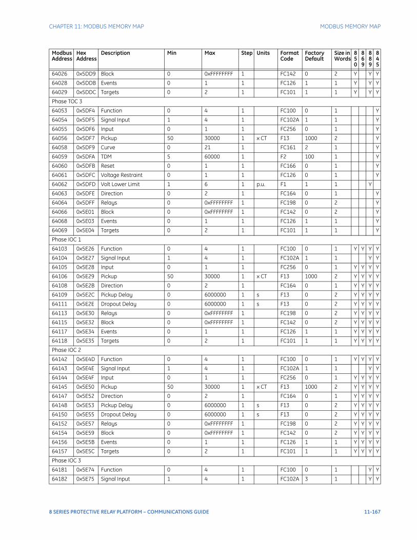
CHAPTER 11: MODBUS MEMORY MAP MODBUS MEMORY MAP
64026 0x5DD9 Block 0 0xFFFFFFFF 1 FC142 0 2 Y Y Y
64028 0x5DDB Events 0 1 1 FC126 1 1 Y Y Y
64029 0x5DDC Targets 0 2 1 FC101 1 1 Y Y Y
Phase TOC 3
64053 0x5DF4 Function 0 4 1 FC100 0 1 Y
64054 0x5DF5 Signal Input 1 4 1 FC102A 1 1 Y
64055 0x5DF6 Input 0 1 1 FC256 0 1 Y
64056 0x5DF7 Pickup 50 30000 1 x CT F13 1000 2 Y
64058 0x5DF9 Curve 0 21 1 FC161 2 1 Y
64059 0x5DFA TDM 5 60000 1 F2 100 1 Y
64060 0x5DFB Reset 0 1 1 FC166 0 1 Y
64061 0x5DFC Voltage Restraint 0 1 1 FC126 0 1 Y
64062 0x5DFD Volt Lower Limit 1 6 1 p.u. F1 1 1 Y
64063 0x5DFE Direction 0 2 1 FC164 0 1 Y
64064 0x5DFF Relays 0 0xFFFFFFFF 1 FC198 0 2 Y
64066 0x5E01 Block 0 0xFFFFFFFF 1 FC142 0 2 Y
64068 0x5E03 Events 0 1 1 FC126 1 1 Y
64069 0x5E04 Targets 0 2 1 FC101 1 1 Y
Phase IOC 1
64103 0x5E26 Function 0 4 1 FC100 0 1 Y Y Y Y
64104 0x5E27 Signal Input 1 4 1 FC102A 1 1 Y Y
64105 0x5E28 Input 0 1 1 FC256 0 1 Y Y Y Y
64106 0x5E29 Pickup 50 30000 1 x CT F13 1000 2 Y Y Y Y
64108 0x5E2B Direction 0 2 1 FC164 0 1 Y Y Y Y
64109 0x5E2C Pickup Delay 0 6000000 1 s F13 0 2 Y Y Y Y
64111 0x5E2E Dropout Delay 0 6000000 1 s F13 0 2 Y Y Y Y
64113 0x5E30 Relays 0 0xFFFFFFFF 1 FC198 0 2 Y Y Y Y
64115 0x5E32 Block 0 0xFFFFFFFF 1 FC142 0 2 Y Y Y Y
64117 0x5E34 Events 0 1 1 FC126 1 1 Y Y Y Y
64118 0x5E35 Targets 0 2 1 FC101 1 1 Y Y Y Y
Phase IOC 2
64142 0x5E4D Function 0 4 1 FC100 0 1 Y Y Y Y
64143 0x5E4E Signal Input 1 4 1 FC102A 1 1 Y Y
64144 0x5E4F Input 0 1 1 FC256 0 1 Y Y Y Y
64145 0x5E50 Pickup 50 30000 1 x CT F13 1000 2 Y Y Y Y
64147 0x5E52 Direction 0 2 1 FC164 0 1 Y Y Y Y
64148 0x5E53 Pickup Delay 0 6000000 1 s F13 0 2 Y Y Y Y
64150 0x5E55 Dropout Delay 0 6000000 1 s F13 0 2 Y Y Y Y
64152 0x5E57 Relays 0 0xFFFFFFFF 1 FC198 0 2 Y Y Y Y
64154 0x5E59 Block 0 0xFFFFFFFF 1 FC142 0 2 Y Y Y Y
64156 0x5E5B Events 0 1 1 FC126 1 1 Y Y Y Y
64157 0x5E5C Targets 0 2 1 FC101 1 1 Y Y Y Y
Phase IOC 3
64181 0x5E74 Function 0 4 1 FC100 0 1 Y Y
64182 0x5E75 Signal Input 1 4 1 FC102A 3 1 Y Y
Modbus Address
Hex Address
Description Min Max Step Units Format Code
Factory Default
Size in Words
850
869
889
845
8 SERIES PROTECTIVE RELAY PLATFORM – COMMUNICATIONS GUIDE 11-167
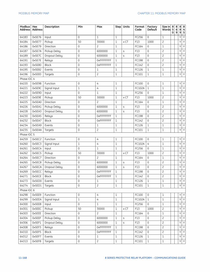
MODBUS MEMORY MAP CHAPTER 11: MODBUS MEMORY MAP
64183 0x5E76 Input 0 1 1 FC256 0 1 Y Y
64184 0x5E77 Pickup 50 30000 1 x CT F13 1000 2 Y Y
64186 0x5E79 Direction 0 2 1 FC164 0 1 Y Y
64187 0x5E7A Pickup Delay 0 6000000 1 s F13 0 2 Y Y
64189 0x5E7C Dropout Delay 0 6000000 1 s F13 0 2 Y Y
64191 0x5E7E Relays 0 0xFFFFFFFF 1 FC198 0 2 Y Y
64193 0x5E80 Block 0 0xFFFFFFFF 1 FC142 0 2 Y Y
64195 0x5E82 Events 0 1 1 FC126 1 1 Y Y
64196 0x5E83 Targets 0 2 1 FC101 1 1 Y Y
Phase IOC 4
64220 0x5E9B Function 0 4 1 FC100 0 1 Y Y
64221 0x5E9C Signal Input 1 4 1 FC102A 1 1 Y Y
64222 0x5E9D Input 0 1 1 FC256 0 1 Y Y
64223 0x5E9E Pickup 50 30000 1 x CT F13 1000 2 Y Y
64225 0x5EA0 Direction 0 2 1 FC164 0 1 Y Y
64226 0x5EA1 Pickup Delay 0 6000000 1 s F13 0 2 Y Y
64228 0x5EA3 Dropout Delay 0 6000000 1 s F13 0 2 Y Y
64230 0x5EA5 Relays 0 0xFFFFFFFF 1 FC198 0 2 Y Y
64232 0x5EA7 Block 0 0xFFFFFFFF 1 FC142 0 2 Y Y
64234 0x5EA9 Events 0 1 1 FC126 1 1 Y Y
64235 0x5EAA Targets 0 2 1 FC101 1 1 Y Y
Phase IOC 5
64259 0x5EC2 Function 0 4 1 FC100 0 1 Y Y
64260 0x5EC3 Signal Input 1 4 1 FC102A 4 1 Y Y
64261 0x5EC4 Input 0 1 1 FC256 0 1 Y Y
64262 0x5EC5 Pickup 50 30000 1 x CT F13 1000 2 Y Y
64264 0x5EC7 Direction 0 2 1 FC164 0 1 Y Y
64265 0x5EC8 Pickup Delay 0 6000000 1 s F13 0 2 Y Y
64267 0x5ECA Dropout Delay 0 6000000 1 s F13 0 2 Y Y
64269 0x5ECC Relays 0 0xFFFFFFFF 1 FC198 0 2 Y Y
64271 0x5ECE Block 0 0xFFFFFFFF 1 FC142 0 2 Y Y
64273 0x5ED0 Events 0 1 1 FC126 1 1 Y Y
64274 0x5ED1 Targets 0 2 1 FC101 1 1 Y Y
Phase IOC 6
64298 0x5EE9 Function 0 4 1 FC100 0 1 Y Y
64299 0x5EEA Signal Input 1 4 1 FC102A 1 1 Y Y
64300 0x5EEB Input 0 1 1 FC256 0 1 Y Y
64301 0x5EEC Pickup 50 30000 1 x CT F13 1000 2 Y Y
64303 0x5EEE Direction 0 2 1 FC164 0 1 Y Y
64304 0x5EEF Pickup Delay 0 6000000 1 s F13 0 2 Y Y
64306 0x5EF1 Dropout Delay 0 6000000 1 s F13 0 2 Y Y
64308 0x5EF3 Relays 0 0xFFFFFFFF 1 FC198 0 2 Y Y
64310 0x5EF5 Block 0 0xFFFFFFFF 1 FC142 0 2 Y Y
64312 0x5EF7 Events 0 1 1 FC126 1 1 Y Y
64313 0x5EF8 Targets 0 2 1 FC101 1 1 Y Y
Modbus Address
Hex Address
Description Min Max Step Units Format Code
Factory Default
Size in Words
850
869
889
845
11-168 8 SERIES PROTECTIVE RELAY PLATFORM – COMMUNICATIONS GUIDE
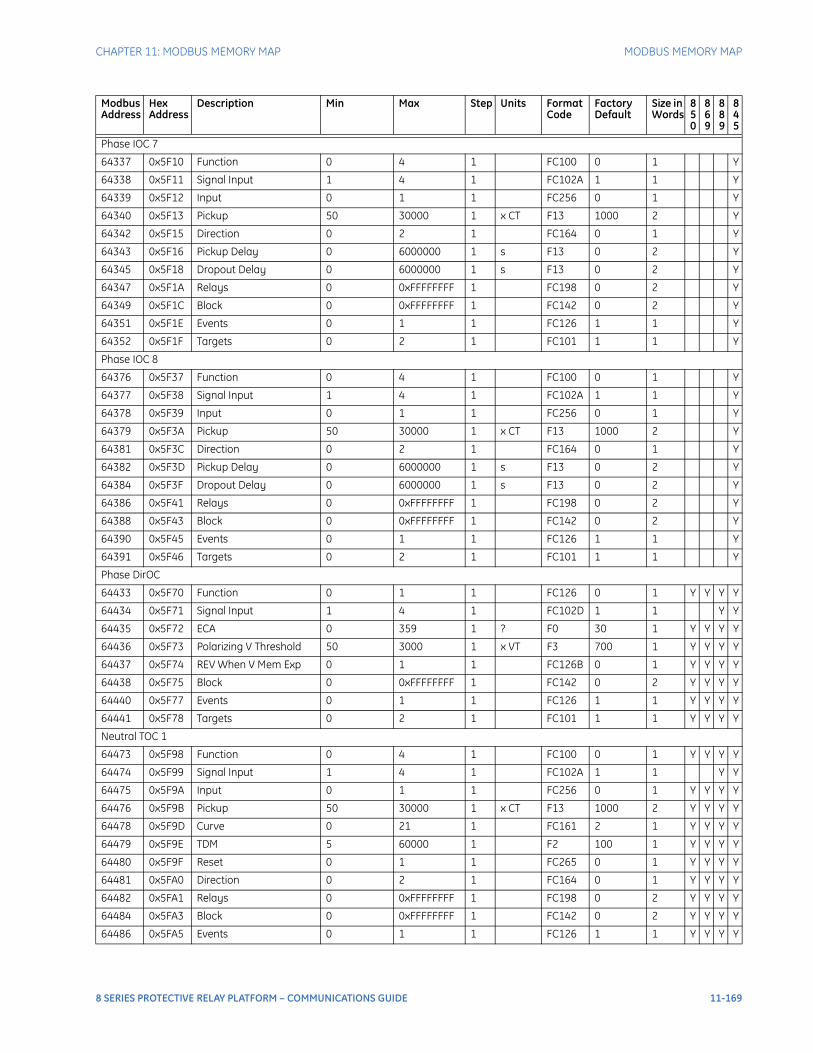
CHAPTER 11: MODBUS MEMORY MAP MODBUS MEMORY MAP
Phase IOC 7
64337 0x5F10 Function 0 4 1 FC100 0 1 Y
64338 0x5F11 Signal Input 1 4 1 FC102A 1 1 Y
64339 0x5F12 Input 0 1 1 FC256 0 1 Y
64340 0x5F13 Pickup 50 30000 1 x CT F13 1000 2 Y
64342 0x5F15 Direction 0 2 1 FC164 0 1 Y
64343 0x5F16 Pickup Delay 0 6000000 1 s F13 0 2 Y
64345 0x5F18 Dropout Delay 0 6000000 1 s F13 0 2 Y
64347 0x5F1A Relays 0 0xFFFFFFFF 1 FC198 0 2 Y
64349 0x5F1C Block 0 0xFFFFFFFF 1 FC142 0 2 Y
64351 0x5F1E Events 0 1 1 FC126 1 1 Y
64352 0x5F1F Targets 0 2 1 FC101 1 1 Y
Phase IOC 8
64376 0x5F37 Function 0 4 1 FC100 0 1 Y
64377 0x5F38 Signal Input 1 4 1 FC102A 1 1 Y
64378 0x5F39 Input 0 1 1 FC256 0 1 Y
64379 0x5F3A Pickup 50 30000 1 x CT F13 1000 2 Y
64381 0x5F3C Direction 0 2 1 FC164 0 1 Y
64382 0x5F3D Pickup Delay 0 6000000 1 s F13 0 2 Y
64384 0x5F3F Dropout Delay 0 6000000 1 s F13 0 2 Y
64386 0x5F41 Relays 0 0xFFFFFFFF 1 FC198 0 2 Y
64388 0x5F43 Block 0 0xFFFFFFFF 1 FC142 0 2 Y
64390 0x5F45 Events 0 1 1 FC126 1 1 Y
64391 0x5F46 Targets 0 2 1 FC101 1 1 Y
Phase DirOC
64433 0x5F70 Function 0 1 1 FC126 0 1 Y Y Y Y
64434 0x5F71 Signal Input 1 4 1 FC102D 1 1 Y Y
64435 0x5F72 ECA 0 359 1 ? F0 30 1 Y Y Y Y
64436 0x5F73 Polarizing V Threshold 50 3000 1 x VT F3 700 1 Y Y Y Y
64437 0x5F74 REV When V Mem Exp 0 1 1 FC126B 0 1 Y Y Y Y
64438 0x5F75 Block 0 0xFFFFFFFF 1 FC142 0 2 Y Y Y Y
64440 0x5F77 Events 0 1 1 FC126 1 1 Y Y Y Y
64441 0x5F78 Targets 0 2 1 FC101 1 1 Y Y Y Y
Neutral TOC 1
64473 0x5F98 Function 0 4 1 FC100 0 1 Y Y Y Y
64474 0x5F99 Signal Input 1 4 1 FC102A 1 1 Y Y
64475 0x5F9A Input 0 1 1 FC256 0 1 Y Y Y Y
64476 0x5F9B Pickup 50 30000 1 x CT F13 1000 2 Y Y Y Y
64478 0x5F9D Curve 0 21 1 FC161 2 1 Y Y Y Y
64479 0x5F9E TDM 5 60000 1 F2 100 1 Y Y Y Y
64480 0x5F9F Reset 0 1 1 FC265 0 1 Y Y Y Y
64481 0x5FA0 Direction 0 2 1 FC164 0 1 Y Y Y Y
64482 0x5FA1 Relays 0 0xFFFFFFFF 1 FC198 0 2 Y Y Y Y
64484 0x5FA3 Block 0 0xFFFFFFFF 1 FC142 0 2 Y Y Y Y
64486 0x5FA5 Events 0 1 1 FC126 1 1 Y Y Y Y
Modbus Address
Hex Address
Description Min Max Step Units Format Code
Factory Default
Size in Words
850
869
889
845
8 SERIES PROTECTIVE RELAY PLATFORM – COMMUNICATIONS GUIDE 11-169
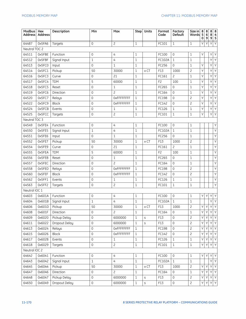
MODBUS MEMORY MAP CHAPTER 11: MODBUS MEMORY MAP
64487 0x5FA6 Targets 0 2 1 FC101 1 1 Y Y Y Y
Neutral TOC 2
64511 0x5FBE Function 0 4 1 FC100 0 1 Y Y Y
64512 0x5FBF Signal Input 1 4 1 FC102A 1 1 Y Y
64513 0x5FC0 Input 0 1 1 FC256 0 1 Y Y Y
64514 0x5FC1 Pickup 50 30000 1 x CT F13 1000 2 Y Y Y
64516 0x5FC3 Curve 0 21 1 FC161 2 1 Y Y Y
64517 0x5FC4 TDM 5 60000 1 F2 100 1 Y Y Y
64518 0x5FC5 Reset 0 1 1 FC265 0 1 Y Y Y
64519 0x5FC6 Direction 0 2 1 FC164 0 1 Y Y Y
64520 0x5FC7 Relays 0 0xFFFFFFFF 1 FC198 0 2 Y Y Y
64522 0x5FC9 Block 0 0xFFFFFFFF 1 FC142 0 2 Y Y Y
64524 0x5FCB Events 0 1 1 FC126 1 1 Y Y Y
64525 0x5FCC Targets 0 2 1 FC101 1 1 Y Y Y
Neutral TOC 3
64549 0x5FE4 Function 0 4 1 FC100 0 1 Y
64550 0x5FE5 Signal Input 1 4 1 FC102A 1 1 Y
64551 0x5FE6 Input 0 1 1 FC256 0 1 Y
64552 0x5FE7 Pickup 50 30000 1 x CT F13 1000 2 Y
64554 0x5FE9 Curve 0 21 1 FC161 2 1 Y
64555 0x5FEA TDM 5 60000 1 F2 100 1 Y
64556 0x5FEB Reset 0 1 1 FC265 0 1 Y
64557 0x5FEC Direction 0 2 1 FC164 0 1 Y
64558 0x5FED Relays 0 0xFFFFFFFF 1 FC198 0 2 Y
64560 0x5FEF Block 0 0xFFFFFFFF 1 FC142 0 2 Y
64562 0x5FF1 Events 0 1 1 FC126 1 1 Y
64563 0x5FF2 Targets 0 2 1 FC101 1 1 Y
Neutral IOC 1
64603 0x601A Function 0 4 1 FC100 0 1 Y Y Y Y
64604 0x601B Signal Input 1 4 1 FC102A 1 1 Y Y
64606 0x601D Pickup 50 30000 1 x CT F13 1000 2 Y Y Y Y
64608 0x601F Direction 0 2 1 FC164 0 1 Y Y Y Y
64609 0x6020 Pickup Delay 0 6000000 1 s F13 0 2 Y Y Y Y
64611 0x6022 Dropout Delay 0 6000000 1 s F13 0 2 Y Y Y Y
64613 0x6024 Relays 0 0xFFFFFFFF 1 FC198 0 2 Y Y Y Y
64615 0x6026 Block 0 0xFFFFFFFF 1 FC142 0 2 Y Y Y Y
64617 0x6028 Events 0 1 1 FC126 1 1 Y Y Y Y
64618 0x6029 Targets 0 2 1 FC101 1 1 Y Y Y Y
Neutral IOC 2
64642 0x6041 Function 0 4 1 FC100 0 1 Y Y Y Y
64643 0x6042 Signal Input 1 4 1 FC102A 1 1 Y Y
64645 0x6044 Pickup 50 30000 1 x CT F13 1000 2 Y Y Y Y
64647 0x6046 Direction 0 2 1 FC164 0 1 Y Y Y Y
64648 0x6047 Pickup Delay 0 6000000 1 s F13 0 2 Y Y Y Y
64650 0x6049 Dropout Delay 0 6000000 1 s F13 0 2 Y Y Y Y
Modbus Address
Hex Address
Description Min Max Step Units Format Code
Factory Default
Size in Words
850
869
889
845
11-170 8 SERIES PROTECTIVE RELAY PLATFORM – COMMUNICATIONS GUIDE
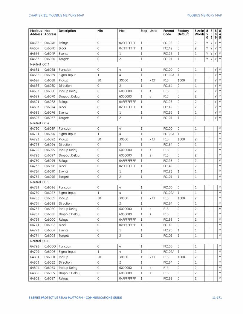
CHAPTER 11: MODBUS MEMORY MAP MODBUS MEMORY MAP
64652 0x604B Relays 0 0xFFFFFFFF 1 FC198 0 2 Y Y Y Y
64654 0x604D Block 0 0xFFFFFFFF 1 FC142 0 2 Y Y Y Y
64656 0x604F Events 0 1 1 FC126 1 1 Y Y Y Y
64657 0x6050 Targets 0 2 1 FC101 1 1 Y Y Y Y
Neutral IOC 3
64681 0x6068 Function 0 4 1 FC100 0 1 Y Y
64682 0x6069 Signal Input 1 4 1 FC102A 1 1 Y Y
64684 0x606B Pickup 50 30000 1 x CT F13 1000 2 Y Y
64686 0x606D Direction 0 2 1 FC164 0 1 Y Y
64687 0x606E Pickup Delay 0 6000000 1 s F13 0 2 Y Y
64689 0x6070 Dropout Delay 0 6000000 1 s F13 0 2 Y Y
64691 0x6072 Relays 0 0xFFFFFFFF 1 FC198 0 2 Y Y
64693 0x6074 Block 0 0xFFFFFFFF 1 FC142 0 2 Y Y
64695 0x6076 Events 0 1 1 FC126 1 1 Y Y
64696 0x6077 Targets 0 2 1 FC101 1 1 Y Y
Neutral IOC 4
64720 0x608F Function 0 4 1 FC100 0 1 Y
64721 0x6090 Signal Input 1 4 1 FC102A 1 1 Y
64723 0x6092 Pickup 50 30000 1 x CT F13 1000 2 Y
64725 0x6094 Direction 0 2 1 FC164 0 1 Y
64726 0x6095 Pickup Delay 0 6000000 1 s F13 0 2 Y
64728 0x6097 Dropout Delay 0 6000000 1 s F13 0 2 Y
64730 0x6099 Relays 0 0xFFFFFFFF 1 FC198 0 2 Y
64732 0x609B Block 0 0xFFFFFFFF 1 FC142 0 2 Y
64734 0x609D Events 0 1 1 FC126 1 1 Y
64735 0x609E Targets 0 2 1 FC101 1 1 Y
Neutral IOC 5
64759 0x60B6 Function 0 4 1 FC100 0 1 Y
64760 0x60B7 Signal Input 1 4 1 FC102A 1 1 Y
64762 0x60B9 Pickup 50 30000 1 x CT F13 1000 2 Y
64764 0x60BB Direction 0 2 1 FC164 0 1 Y
64765 0x60BC Pickup Delay 0 6000000 1 s F13 0 2 Y
64767 0x60BE Dropout Delay 0 6000000 1 s F13 0 2 Y
64769 0x60C0 Relays 0 0xFFFFFFFF 1 FC198 0 2 Y
64771 0x60C2 Block 0 0xFFFFFFFF 1 FC142 0 2 Y
64773 0x60C4 Events 0 1 1 FC126 1 1 Y
64774 0x60C5 Targets 0 2 1 FC101 1 1 Y
Neutral IOC 6
64798 0x60DD Function 0 4 1 FC100 0 1 Y
64799 0x60DE Signal Input 1 4 1 FC102A 1 1 Y
64801 0x60E0 Pickup 50 30000 1 x CT F13 1000 2 Y
64803 0x60E2 Direction 0 2 1 FC164 0 1 Y
64804 0x60E3 Pickup Delay 0 6000000 1 s F13 0 2 Y
64806 0x60E5 Dropout Delay 0 6000000 1 s F13 0 2 Y
64808 0x60E7 Relays 0 0xFFFFFFFF 1 FC198 0 2 Y
Modbus Address
Hex Address
Description Min Max Step Units Format Code
Factory Default
Size in Words
850
869
889
845
8 SERIES PROTECTIVE RELAY PLATFORM – COMMUNICATIONS GUIDE 11-171
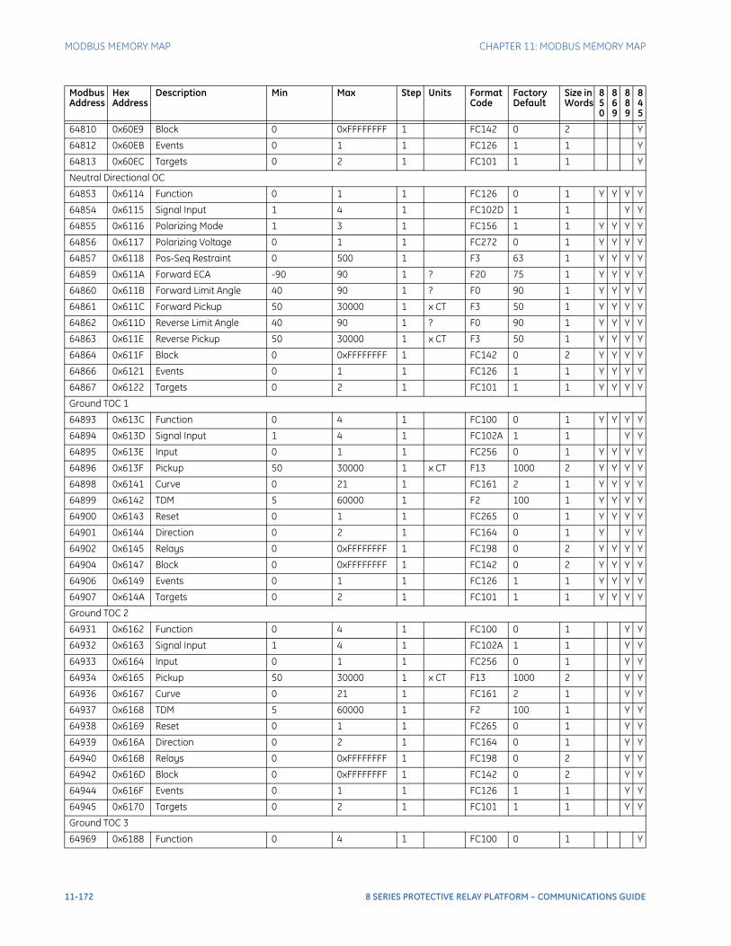
MODBUS MEMORY MAP CHAPTER 11: MODBUS MEMORY MAP
64810 0x60E9 Block 0 0xFFFFFFFF 1 FC142 0 2 Y
64812 0x60EB Events 0 1 1 FC126 1 1 Y
64813 0x60EC Targets 0 2 1 FC101 1 1 Y
Neutral Directional OC
64853 0x6114 Function 0 1 1 FC126 0 1 Y Y Y Y
64854 0x6115 Signal Input 1 4 1 FC102D 1 1 Y Y
64855 0x6116 Polarizing Mode 1 3 1 FC156 1 1 Y Y Y Y
64856 0x6117 Polarizing Voltage 0 1 1 FC272 0 1 Y Y Y Y
64857 0x6118 Pos-Seq Restraint 0 500 1 F3 63 1 Y Y Y Y
64859 0x611A Forward ECA -90 90 1 ? F20 75 1 Y Y Y Y
64860 0x611B Forward Limit Angle 40 90 1 ? F0 90 1 Y Y Y Y
64861 0x611C Forward Pickup 50 30000 1 x CT F3 50 1 Y Y Y Y
64862 0x611D Reverse Limit Angle 40 90 1 ? F0 90 1 Y Y Y Y
64863 0x611E Reverse Pickup 50 30000 1 x CT F3 50 1 Y Y Y Y
64864 0x611F Block 0 0xFFFFFFFF 1 FC142 0 2 Y Y Y Y
64866 0x6121 Events 0 1 1 FC126 1 1 Y Y Y Y
64867 0x6122 Targets 0 2 1 FC101 1 1 Y Y Y Y
Ground TOC 1
64893 0x613C Function 0 4 1 FC100 0 1 Y Y Y Y
64894 0x613D Signal Input 1 4 1 FC102A 1 1 Y Y
64895 0x613E Input 0 1 1 FC256 0 1 Y Y Y Y
64896 0x613F Pickup 50 30000 1 x CT F13 1000 2 Y Y Y Y
64898 0x6141 Curve 0 21 1 FC161 2 1 Y Y Y Y
64899 0x6142 TDM 5 60000 1 F2 100 1 Y Y Y Y
64900 0x6143 Reset 0 1 1 FC265 0 1 Y Y Y Y
64901 0x6144 Direction 0 2 1 FC164 0 1 Y Y Y
64902 0x6145 Relays 0 0xFFFFFFFF 1 FC198 0 2 Y Y Y Y
64904 0x6147 Block 0 0xFFFFFFFF 1 FC142 0 2 Y Y Y Y
64906 0x6149 Events 0 1 1 FC126 1 1 Y Y Y Y
64907 0x614A Targets 0 2 1 FC101 1 1 Y Y Y Y
Ground TOC 2
64931 0x6162 Function 0 4 1 FC100 0 1 Y Y
64932 0x6163 Signal Input 1 4 1 FC102A 1 1 Y Y
64933 0x6164 Input 0 1 1 FC256 0 1 Y Y
64934 0x6165 Pickup 50 30000 1 x CT F13 1000 2 Y Y
64936 0x6167 Curve 0 21 1 FC161 2 1 Y Y
64937 0x6168 TDM 5 60000 1 F2 100 1 Y Y
64938 0x6169 Reset 0 1 1 FC265 0 1 Y Y
64939 0x616A Direction 0 2 1 FC164 0 1 Y Y
64940 0x616B Relays 0 0xFFFFFFFF 1 FC198 0 2 Y Y
64942 0x616D Block 0 0xFFFFFFFF 1 FC142 0 2 Y Y
64944 0x616F Events 0 1 1 FC126 1 1 Y Y
64945 0x6170 Targets 0 2 1 FC101 1 1 Y Y
Ground TOC 3
64969 0x6188 Function 0 4 1 FC100 0 1 Y
Modbus Address
Hex Address
Description Min Max Step Units Format Code
Factory Default
Size in Words
850
869
889
845
11-172 8 SERIES PROTECTIVE RELAY PLATFORM – COMMUNICATIONS GUIDE
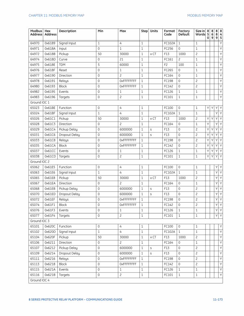
CHAPTER 11: MODBUS MEMORY MAP MODBUS MEMORY MAP
64970 0x6189 Signal Input 1 4 1 FC102A 1 1 Y
64971 0x618A Input 0 1 1 FC256 0 1 Y
64972 0x618B Pickup 50 30000 1 x CT F13 1000 2 Y
64974 0x618D Curve 0 21 1 FC161 2 1 Y
64975 0x618E TDM 5 60000 1 F2 100 1 Y
64976 0x618F Reset 0 1 1 FC265 0 1 Y
64977 0x6190 Direction 0 2 1 FC164 0 1 Y
64978 0x6191 Relays 0 0xFFFFFFFF 1 FC198 0 2 Y
64980 0x6193 Block 0 0xFFFFFFFF 1 FC142 0 2 Y
64982 0x6195 Events 0 1 1 FC126 1 1 Y
64983 0x6196 Targets 0 2 1 FC101 1 1 Y
Ground IOC 1
65023 0x61BE Function 0 4 1 FC100 0 1 Y Y Y Y
65024 0x61BF Signal Input 1 4 1 FC102A 1 1 Y Y
65026 0x61C1 Pickup 50 30000 1 x CT F13 1000 2 Y Y Y Y
65028 0x61C3 Direction 0 2 1 FC164 0 1 Y Y Y
65029 0x61C4 Pickup Delay 0 6000000 1 s F13 0 2 Y Y Y Y
65031 0x61C6 Dropout Delay 0 6000000 1 s F13 0 2 Y Y Y Y
65033 0x61C8 Relays 0 0xFFFFFFFF 1 FC198 0 2 Y Y Y Y
65035 0x61CA Block 0 0xFFFFFFFF 1 FC142 0 2 Y Y Y Y
65037 0x61CC Events 0 1 1 FC126 1 1 Y Y Y Y
65038 0x61CD Targets 0 2 1 FC101 1 1 Y Y Y Y
Ground IOC 2
65062 0x61E5 Function 0 4 1 FC100 0 1 Y Y
65063 0x61E6 Signal Input 1 4 1 FC102A 1 1 Y Y
65065 0x61E8 Pickup 50 30000 1 x CT F13 1000 2 Y Y
65067 0x61EA Direction 0 2 1 FC164 0 1 Y Y
65068 0x61EB Pickup Delay 0 6000000 1 s F13 0 2 Y Y
65070 0x61ED Dropout Delay 0 6000000 1 s F13 0 2 Y Y
65072 0x61EF Relays 0 0xFFFFFFFF 1 FC198 0 2 Y Y
65074 0x61F1 Block 0 0xFFFFFFFF 1 FC142 0 2 Y Y
65076 0x61F3 Events 0 1 1 FC126 1 1 Y Y
65077 0x61F4 Targets 0 2 1 FC101 1 1 Y Y
Ground IOC 3
65101 0x620C Function 0 4 1 FC100 0 1 Y
65102 0x620D Signal Input 1 4 1 FC102A 1 1 Y
65104 0x620F Pickup 50 30000 1 x CT F13 1000 2 Y
65106 0x6211 Direction 0 2 1 FC164 0 1 Y
65107 0x6212 Pickup Delay 0 6000000 1 s F13 0 2 Y
65109 0x6214 Dropout Delay 0 6000000 1 s F13 0 2 Y
65111 0x6216 Relays 0 0xFFFFFFFF 1 FC198 0 2 Y
65113 0x6218 Block 0 0xFFFFFFFF 1 FC142 0 2 Y
65115 0x621A Events 0 1 1 FC126 1 1 Y
65116 0x621B Targets 0 2 1 FC101 1 1 Y
Ground IOC 4
Modbus Address
Hex Address
Description Min Max Step Units Format Code
Factory Default
Size in Words
850
869
889
845
8 SERIES PROTECTIVE RELAY PLATFORM – COMMUNICATIONS GUIDE 11-173
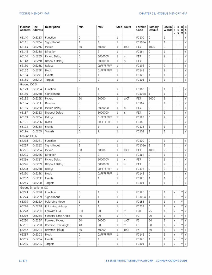
MODBUS MEMORY MAP CHAPTER 11: MODBUS MEMORY MAP
65140 0x6233 Function 0 4 1 FC100 0 1 Y
65141 0x6234 Signal Input 1 4 1 FC102A 1 1 Y
65143 0x6236 Pickup 50 30000 1 x CT F13 1000 2 Y
65145 0x6238 Direction 0 2 1 FC164 0 1 Y
65146 0x6239 Pickup Delay 0 6000000 1 s F13 0 2 Y
65148 0x623B Dropout Delay 0 6000000 1 s F13 0 2 Y
65150 0x623D Relays 0 0xFFFFFFFF 1 FC198 0 2 Y
65152 0x623F Block 0 0xFFFFFFFF 1 FC142 0 2 Y
65154 0x6241 Events 0 1 1 FC126 1 1 Y
65155 0x6242 Targets 0 2 1 FC101 1 1 Y
Ground IOC 5
65179 0x625A Function 0 4 1 FC100 0 1 Y
65180 0x625B Signal Input 1 4 1 FC102A 1 1 Y
65182 0x625D Pickup 50 30000 1 x CT F13 1000 2 Y
65184 0x625F Direction 0 2 1 FC164 0 1 Y
65185 0x6260 Pickup Delay 0 6000000 1 s F13 0 2 Y
65187 0x6262 Dropout Delay 0 6000000 1 s F13 0 2 Y
65189 0x6264 Relays 0 0xFFFFFFFF 1 FC198 0 2 Y
65191 0x6266 Block 0 0xFFFFFFFF 1 FC142 0 2 Y
65193 0x6268 Events 0 1 1 FC126 1 1 Y
65194 0x6269 Targets 0 2 1 FC101 1 1 Y
Ground IOC 6
65218 0x6281 Function 0 4 1 FC100 0 1 Y
65219 0x6282 Signal Input 1 4 1 FC102A 1 1 Y
65221 0x6284 Pickup 50 30000 1 x CT F13 1000 2 Y
65223 0x6286 Direction 0 2 1 FC164 0 1 Y
65224 0x6287 Pickup Delay 0 6000000 1 s F13 0 2 Y
65226 0x6289 Dropout Delay 0 6000000 1 s F13 0 2 Y
65228 0x628B Relays 0 0xFFFFFFFF 1 FC198 0 2 Y
65230 0x628D Block 0 0xFFFFFFFF 1 FC142 0 2 Y
65232 0x628F Events 0 1 1 FC126 1 1 Y
65233 0x6290 Targets 0 2 1 FC101 1 1 Y
Ground Directional OC
65273 0x62B8 Function 0 1 1 FC126 0 1 Y Y Y
65274 0x62B9 Signal Input 1 4 1 FC102A 1 1 Y Y
65275 0x62BA Polarizing Mode 1 3 1 FC156 1 1 Y Y
65276 0x62BB Polarizing Voltage 0 1 1 FC272 0 1 Y Y Y
65278 0x62BD Forward ECA -90 90 1 ? F20 75 1 Y Y Y
65279 0x62BE Forward Limit Angle 40 90 1 ? F0 90 1 Y Y Y
65280 0x62BF Forward Pickup 50 30000 1 x CT F3 50 1 Y Y Y
65281 0x62C0 Reverse Limit Angle 40 90 1 ? F0 90 1 Y Y Y
65282 0x62C1 Reverse Pickup 50 30000 1 x CT F3 50 1 Y Y Y
65283 0x62C2 Block 0 0xFFFFFFFF 1 FC142 0 2 Y Y Y
65285 0x62C4 Events 0 1 1 FC126 1 1 Y Y Y
65286 0x62C5 Targets 0 2 1 FC101 1 1 Y Y Y
Modbus Address
Hex Address
Description Min Max Step Units Format Code
Factory Default
Size in Words
850
869
889
845
11-174 8 SERIES PROTECTIVE RELAY PLATFORM – COMMUNICATIONS GUIDE
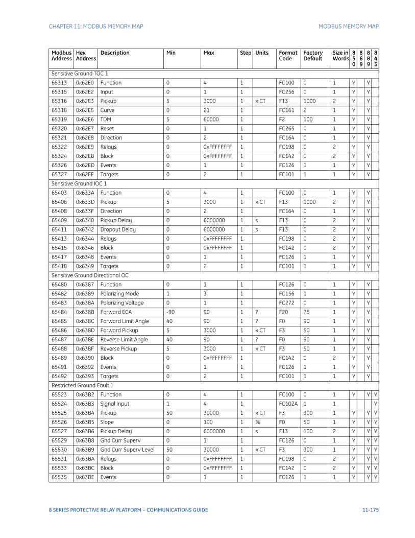
CHAPTER 11: MODBUS MEMORY MAP MODBUS MEMORY MAP
Sensitive Ground TOC 1
65313 0x62E0 Function 0 4 1 FC100 0 1 Y Y
65315 0x62E2 Input 0 1 1 FC256 0 1 Y Y
65316 0x62E3 Pickup 5 3000 1 x CT F13 1000 2 Y Y
65318 0x62E5 Curve 0 21 1 FC161 2 1 Y Y
65319 0x62E6 TDM 5 60000 1 F2 100 1 Y Y
65320 0x62E7 Reset 0 1 1 FC265 0 1 Y Y
65321 0x62E8 Direction 0 2 1 FC164 0 1 Y Y
65322 0x62E9 Relays 0 0xFFFFFFFF 1 FC198 0 2 Y Y
65324 0x62EB Block 0 0xFFFFFFFF 1 FC142 0 2 Y Y
65326 0x62ED Events 0 1 1 FC126 1 1 Y Y
65327 0x62EE Targets 0 2 1 FC101 1 1 Y Y
Sensitive Ground IOC 1
65403 0x633A Function 0 4 1 FC100 0 1 Y Y
65406 0x633D Pickup 5 3000 1 x CT F13 1000 2 Y Y
65408 0x633F Direction 0 2 1 FC164 0 1 Y Y
65409 0x6340 Pickup Delay 0 6000000 1 s F13 0 2 Y Y
65411 0x6342 Dropout Delay 0 6000000 1 s F13 0 2 Y Y
65413 0x6344 Relays 0 0xFFFFFFFF 1 FC198 0 2 Y Y
65415 0x6346 Block 0 0xFFFFFFFF 1 FC142 0 2 Y Y
65417 0x6348 Events 0 1 1 FC126 1 1 Y Y
65418 0x6349 Targets 0 2 1 FC101 1 1 Y Y
Sensitive Ground Directional OC
65480 0x6387 Function 0 1 1 FC126 0 1 Y Y
65482 0x6389 Polarizing Mode 1 3 1 FC156 1 1 Y Y
65483 0x638A Polarizing Voltage 0 1 1 FC272 0 1 Y Y
65484 0x638B Forward ECA -90 90 1 ? F20 75 1 Y Y
65485 0x638C Forward Limit Angle 40 90 1 ? F0 90 1 Y Y
65486 0x638D Forward Pickup 5 3000 1 x CT F3 50 1 Y Y
65487 0x638E Reverse Limit Angle 40 90 1 ? F0 90 1 Y Y
65488 0x638F Reverse Pickup 5 3000 1 x CT F3 50 1 Y Y
65489 0x6390 Block 0 0xFFFFFFFF 1 FC142 0 2 Y Y
65491 0x6392 Events 0 1 1 FC126 1 1 Y Y
65492 0x6393 Targets 0 2 1 FC101 1 1 Y Y
Restricted Ground Fault 1
65523 0x63B2 Function 0 4 1 FC100 0 1 Y Y Y
65524 0x63B3 Signal Input 1 4 1 FC102A 1 1 Y
65525 0x63B4 Pickup 50 30000 1 x CT F3 300 1 Y Y Y
65526 0x63B5 Slope 0 100 1 % F0 50 1 Y Y Y
65527 0x63B6 Pickup Delay 0 6000000 1 s F13 100 2 Y Y Y
65529 0x63B8 Gnd Curr Superv 0 1 1 FC126 0 1 Y Y Y
65530 0x63B9 Gnd Curr Superv Level 50 30000 1 x CT F3 300 1 Y Y Y
65531 0x63BA Relays 0 0xFFFFFFFF 1 FC198 0 2 Y Y Y
65533 0x63BC Block 0 0xFFFFFFFF 1 FC142 0 2 Y Y Y
65535 0x63BE Events 0 1 1 FC126 1 1 Y Y Y
Modbus Address
Hex Address
Description Min Max Step Units Format Code
Factory Default
Size in Words
850
869
889
845
8 SERIES PROTECTIVE RELAY PLATFORM – COMMUNICATIONS GUIDE 11-175
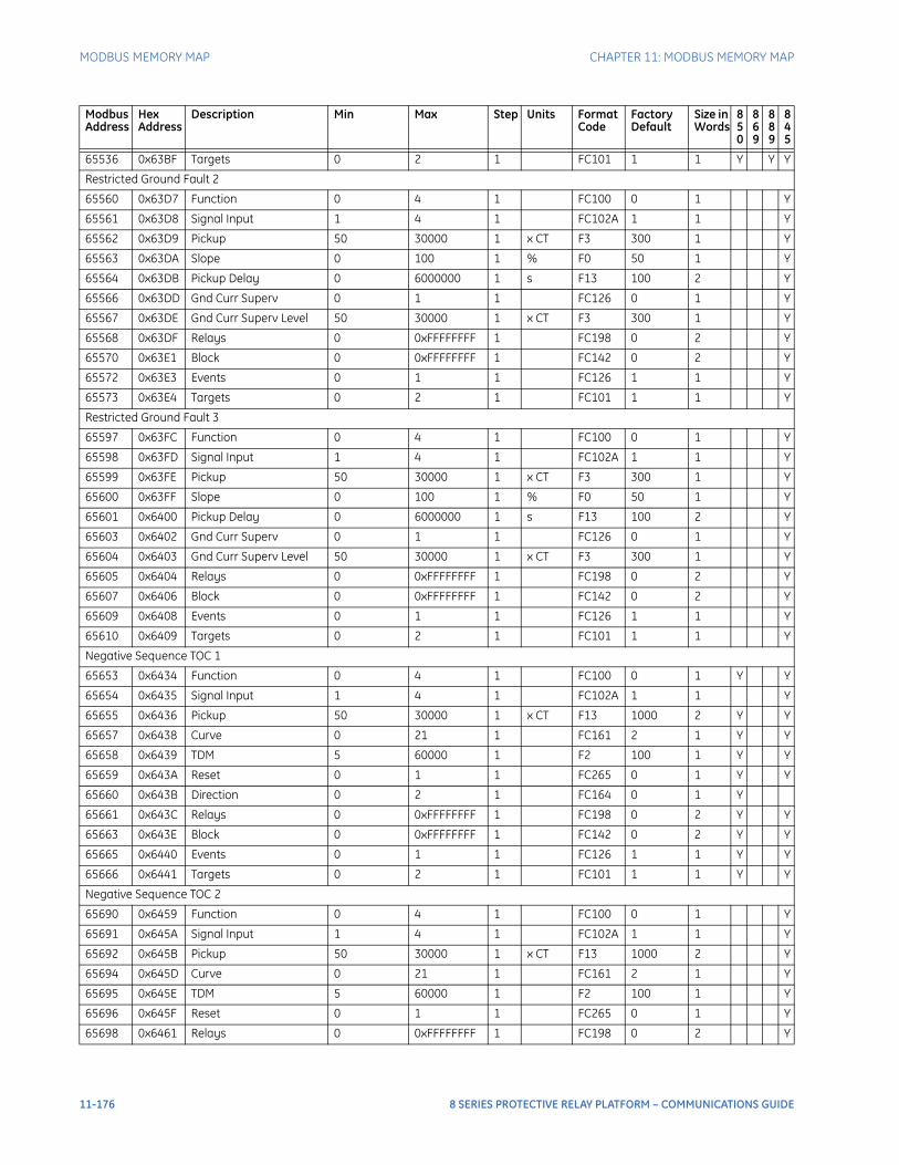
MODBUS MEMORY MAP CHAPTER 11: MODBUS MEMORY MAP
65536 0x63BF Targets 0 2 1 FC101 1 1 Y Y Y
Restricted Ground Fault 2
65560 0x63D7 Function 0 4 1 FC100 0 1 Y
65561 0x63D8 Signal Input 1 4 1 FC102A 1 1 Y
65562 0x63D9 Pickup 50 30000 1 x CT F3 300 1 Y
65563 0x63DA Slope 0 100 1 % F0 50 1 Y
65564 0x63DB Pickup Delay 0 6000000 1 s F13 100 2 Y
65566 0x63DD Gnd Curr Superv 0 1 1 FC126 0 1 Y
65567 0x63DE Gnd Curr Superv Level 50 30000 1 x CT F3 300 1 Y
65568 0x63DF Relays 0 0xFFFFFFFF 1 FC198 0 2 Y
65570 0x63E1 Block 0 0xFFFFFFFF 1 FC142 0 2 Y
65572 0x63E3 Events 0 1 1 FC126 1 1 Y
65573 0x63E4 Targets 0 2 1 FC101 1 1 Y
Restricted Ground Fault 3
65597 0x63FC Function 0 4 1 FC100 0 1 Y
65598 0x63FD Signal Input 1 4 1 FC102A 1 1 Y
65599 0x63FE Pickup 50 30000 1 x CT F3 300 1 Y
65600 0x63FF Slope 0 100 1 % F0 50 1 Y
65601 0x6400 Pickup Delay 0 6000000 1 s F13 100 2 Y
65603 0x6402 Gnd Curr Superv 0 1 1 FC126 0 1 Y
65604 0x6403 Gnd Curr Superv Level 50 30000 1 x CT F3 300 1 Y
65605 0x6404 Relays 0 0xFFFFFFFF 1 FC198 0 2 Y
65607 0x6406 Block 0 0xFFFFFFFF 1 FC142 0 2 Y
65609 0x6408 Events 0 1 1 FC126 1 1 Y
65610 0x6409 Targets 0 2 1 FC101 1 1 Y
Negative Sequence TOC 1
65653 0x6434 Function 0 4 1 FC100 0 1 Y Y
65654 0x6435 Signal Input 1 4 1 FC102A 1 1 Y
65655 0x6436 Pickup 50 30000 1 x CT F13 1000 2 Y Y
65657 0x6438 Curve 0 21 1 FC161 2 1 Y Y
65658 0x6439 TDM 5 60000 1 F2 100 1 Y Y
65659 0x643A Reset 0 1 1 FC265 0 1 Y Y
65660 0x643B Direction 0 2 1 FC164 0 1 Y
65661 0x643C Relays 0 0xFFFFFFFF 1 FC198 0 2 Y Y
65663 0x643E Block 0 0xFFFFFFFF 1 FC142 0 2 Y Y
65665 0x6440 Events 0 1 1 FC126 1 1 Y Y
65666 0x6441 Targets 0 2 1 FC101 1 1 Y Y
Negative Sequence TOC 2
65690 0x6459 Function 0 4 1 FC100 0 1 Y
65691 0x645A Signal Input 1 4 1 FC102A 1 1 Y
65692 0x645B Pickup 50 30000 1 x CT F13 1000 2 Y
65694 0x645D Curve 0 21 1 FC161 2 1 Y
65695 0x645E TDM 5 60000 1 F2 100 1 Y
65696 0x645F Reset 0 1 1 FC265 0 1 Y
65698 0x6461 Relays 0 0xFFFFFFFF 1 FC198 0 2 Y
Modbus Address
Hex Address
Description Min Max Step Units Format Code
Factory Default
Size in Words
850
869
889
845
11-176 8 SERIES PROTECTIVE RELAY PLATFORM – COMMUNICATIONS GUIDE
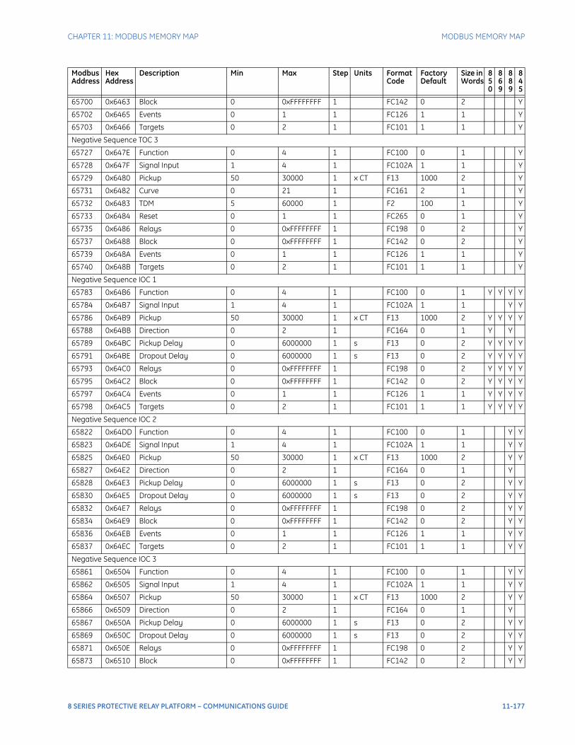
CHAPTER 11: MODBUS MEMORY MAP MODBUS MEMORY MAP
65700 0x6463 Block 0 0xFFFFFFFF 1 FC142 0 2 Y
65702 0x6465 Events 0 1 1 FC126 1 1 Y
65703 0x6466 Targets 0 2 1 FC101 1 1 Y
Negative Sequence TOC 3
65727 0x647E Function 0 4 1 FC100 0 1 Y
65728 0x647F Signal Input 1 4 1 FC102A 1 1 Y
65729 0x6480 Pickup 50 30000 1 x CT F13 1000 2 Y
65731 0x6482 Curve 0 21 1 FC161 2 1 Y
65732 0x6483 TDM 5 60000 1 F2 100 1 Y
65733 0x6484 Reset 0 1 1 FC265 0 1 Y
65735 0x6486 Relays 0 0xFFFFFFFF 1 FC198 0 2 Y
65737 0x6488 Block 0 0xFFFFFFFF 1 FC142 0 2 Y
65739 0x648A Events 0 1 1 FC126 1 1 Y
65740 0x648B Targets 0 2 1 FC101 1 1 Y
Negative Sequence IOC 1
65783 0x64B6 Function 0 4 1 FC100 0 1 Y Y Y Y
65784 0x64B7 Signal Input 1 4 1 FC102A 1 1 Y Y
65786 0x64B9 Pickup 50 30000 1 x CT F13 1000 2 Y Y Y Y
65788 0x64BB Direction 0 2 1 FC164 0 1 Y Y
65789 0x64BC Pickup Delay 0 6000000 1 s F13 0 2 Y Y Y Y
65791 0x64BE Dropout Delay 0 6000000 1 s F13 0 2 Y Y Y Y
65793 0x64C0 Relays 0 0xFFFFFFFF 1 FC198 0 2 Y Y Y Y
65795 0x64C2 Block 0 0xFFFFFFFF 1 FC142 0 2 Y Y Y Y
65797 0x64C4 Events 0 1 1 FC126 1 1 Y Y Y Y
65798 0x64C5 Targets 0 2 1 FC101 1 1 Y Y Y Y
Negative Sequence IOC 2
65822 0x64DD Function 0 4 1 FC100 0 1 Y Y
65823 0x64DE Signal Input 1 4 1 FC102A 1 1 Y Y
65825 0x64E0 Pickup 50 30000 1 x CT F13 1000 2 Y Y
65827 0x64E2 Direction 0 2 1 FC164 0 1 Y
65828 0x64E3 Pickup Delay 0 6000000 1 s F13 0 2 Y Y
65830 0x64E5 Dropout Delay 0 6000000 1 s F13 0 2 Y Y
65832 0x64E7 Relays 0 0xFFFFFFFF 1 FC198 0 2 Y Y
65834 0x64E9 Block 0 0xFFFFFFFF 1 FC142 0 2 Y Y
65836 0x64EB Events 0 1 1 FC126 1 1 Y Y
65837 0x64EC Targets 0 2 1 FC101 1 1 Y Y
Negative Sequence IOC 3
65861 0x6504 Function 0 4 1 FC100 0 1 Y Y
65862 0x6505 Signal Input 1 4 1 FC102A 1 1 Y Y
65864 0x6507 Pickup 50 30000 1 x CT F13 1000 2 Y Y
65866 0x6509 Direction 0 2 1 FC164 0 1 Y
65867 0x650A Pickup Delay 0 6000000 1 s F13 0 2 Y Y
65869 0x650C Dropout Delay 0 6000000 1 s F13 0 2 Y Y
65871 0x650E Relays 0 0xFFFFFFFF 1 FC198 0 2 Y Y
65873 0x6510 Block 0 0xFFFFFFFF 1 FC142 0 2 Y Y
Modbus Address
Hex Address
Description Min Max Step Units Format Code
Factory Default
Size in Words
850
869
889
845
8 SERIES PROTECTIVE RELAY PLATFORM – COMMUNICATIONS GUIDE 11-177
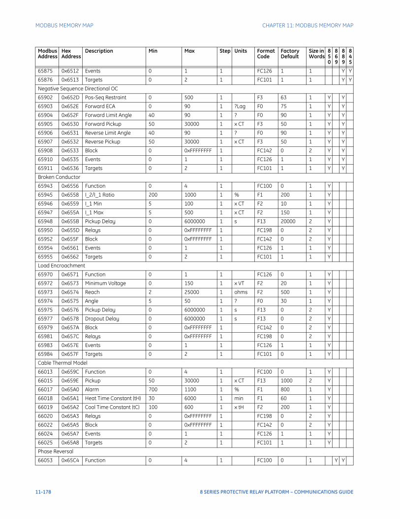
MODBUS MEMORY MAP CHAPTER 11: MODBUS MEMORY MAP
65875 0x6512 Events 0 1 1 FC126 1 1 Y Y
65876 0x6513 Targets 0 2 1 FC101 1 1 Y Y
Negative Sequence Directional OC
65902 0x652D Pos-Seq Restraint 0 500 1 F3 63 1 Y Y
65903 0x652E Forward ECA 0 90 1 ?Lag F0 75 1 Y Y
65904 0x652F Forward Limit Angle 40 90 1 ? F0 90 1 Y Y
65905 0x6530 Forward Pickup 50 30000 1 x CT F3 50 1 Y Y
65906 0x6531 Reverse Limit Angle 40 90 1 ? F0 90 1 Y Y
65907 0x6532 Reverse Pickup 50 30000 1 x CT F3 50 1 Y Y
65908 0x6533 Block 0 0xFFFFFFFF 1 FC142 0 2 Y Y
65910 0x6535 Events 0 1 1 FC126 1 1 Y Y
65911 0x6536 Targets 0 2 1 FC101 1 1 Y Y
Broken Conductor
65943 0x6556 Function 0 4 1 FC100 0 1 Y
65945 0x6558 I_2/I_1 Ratio 200 1000 1 % F1 200 1 Y
65946 0x6559 I_1 Min 5 100 1 x CT F2 10 1 Y
65947 0x655A I_1 Max 5 500 1 x CT F2 150 1 Y
65948 0x655B Pickup Delay 0 6000000 1 s F13 20000 2 Y
65950 0x655D Relays 0 0xFFFFFFFF 1 FC198 0 2 Y
65952 0x655F Block 0 0xFFFFFFFF 1 FC142 0 2 Y
65954 0x6561 Events 0 1 1 FC126 1 1 Y
65955 0x6562 Targets 0 2 1 FC101 1 1 Y
Load Encroachment
65970 0x6571 Function 0 1 1 FC126 0 1 Y
65972 0x6573 Minimum Voltage 0 150 1 x VT F2 20 1 Y
65973 0x6574 Reach 2 25000 1 ohms F2 500 1 Y
65974 0x6575 Angle 5 50 1 ? F0 30 1 Y
65975 0x6576 Pickup Delay 0 6000000 1 s F13 0 2 Y
65977 0x6578 Dropout Delay 0 6000000 1 s F13 0 2 Y
65979 0x657A Block 0 0xFFFFFFFF 1 FC142 0 2 Y
65981 0x657C Relays 0 0xFFFFFFFF 1 FC198 0 2 Y
65983 0x657E Events 0 1 1 FC126 1 1 Y
65984 0x657F Targets 0 2 1 FC101 0 1 Y
Cable Thermal Model
66013 0x659C Function 0 4 1 FC100 0 1 Y
66015 0x659E Pickup 50 30000 1 x CT F13 1000 2 Y
66017 0x65A0 Alarm 700 1100 1 % F1 800 1 Y
66018 0x65A1 Heat Time Constant (tH) 30 6000 1 min F1 60 1 Y
66019 0x65A2 Cool Time Constant (tC) 100 600 1 x tH F2 200 1 Y
66020 0x65A3 Relays 0 0xFFFFFFFF 1 FC198 0 2 Y
66022 0x65A5 Block 0 0xFFFFFFFF 1 FC142 0 2 Y
66024 0x65A7 Events 0 1 1 FC126 1 1 Y
66025 0x65A8 Targets 0 2 1 FC101 1 1 Y
Phase Reversal
66053 0x65C4 Function 0 4 1 FC100 0 1 Y Y
Modbus Address
Hex Address
Description Min Max Step Units Format Code
Factory Default
Size in Words
850
869
889
845
11-178 8 SERIES PROTECTIVE RELAY PLATFORM – COMMUNICATIONS GUIDE
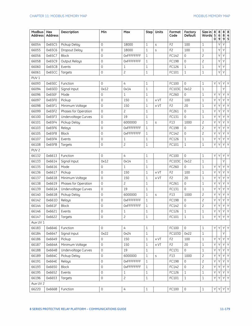
CHAPTER 11: MODBUS MEMORY MAP MODBUS MEMORY MAP
66054 0x65C5 Pickup Delay 0 18000 1 s F2 100 1 Y Y
66055 0x65C6 Dropout Delay 0 18000 1 s F2 100 1 Y Y
66056 0x65C7 Block 0 0xFFFFFFFF 1 FC142 0 2 Y Y
66058 0x65C9 Output Relays 0 0xFFFFFFFF 1 FC198 0 2 Y Y
66060 0x65CB Events 0 1 1 FC126 1 1 Y Y
66061 0x65CC Targets 0 2 1 FC101 1 1 Y Y
PUV 1
66093 0x65EC Function 0 4 1 FC100 0 1 Y Y Y Y
66094 0x65ED Signal Input 0x12 0x14 1 FC103C 0x12 1 Y
66096 0x65EF Mode 0 1 1 FC260 0 1 Y Y Y Y
66097 0x65F0 Pickup 0 150 1 x VT F2 100 1 Y Y Y Y
66098 0x65F1 Minimum Voltage 0 150 1 x VT F2 20 1 Y Y Y Y
66099 0x65F2 Phases for Operation 0 2 1 FC261 0 1 Y Y Y Y
66100 0x65F3 Undervoltage Curves 0 19 1 FC131 0 1 Y Y Y Y
66101 0x65F4 Pickup Delay 0 6000000 1 s F13 1000 2 Y Y Y Y
66103 0x65F6 Relays 0 0xFFFFFFFF 1 FC198 0 2 Y Y Y Y
66105 0x65F8 Block 0 0xFFFFFFFF 1 FC142 0 2 Y Y Y Y
66107 0x65FA Events 0 1 1 FC126 1 1 Y Y Y Y
66108 0x65FB Targets 0 2 1 FC101 1 1 Y Y Y Y
PUV 2
66132 0x6613 Function 0 4 1 FC100 0 1 Y Y Y Y
66133 0x6614 Signal Input 0x12 0x14 1 FC103C 0x12 1 Y
66135 0x6616 Mode 0 1 1 FC260 0 1 Y Y Y Y
66136 0x6617 Pickup 0 150 1 x VT F2 100 1 Y Y Y Y
66137 0x6618 Minimum Voltage 0 150 1 x VT F2 20 1 Y Y Y Y
66138 0x6619 Phases for Operation 0 2 1 FC261 0 1 Y Y Y Y
66139 0x661A Undervoltage Curves 0 19 1 FC131 0 1 Y Y Y Y
66140 0x661B Pickup Delay 0 6000000 1 s F13 1000 2 Y Y Y Y
66142 0x661D Relays 0 0xFFFFFFFF 1 FC198 0 2 Y Y Y Y
66144 0x661F Block 0 0xFFFFFFFF 1 FC142 0 2 Y Y Y Y
66146 0x6621 Events 0 1 1 FC126 1 1 Y Y Y Y
66147 0x6622 Targets 0 2 1 FC101 1 1 Y Y Y Y
Aux UV 1
66183 0x6646 Function 0 4 1 FC100 0 1 Y Y Y Y
66184 0x6647 Signal Input 0x22 0x24 1 FC103D 0x22 1 Y
66186 0x6649 Pickup 0 150 1 x VT F2 100 1 Y Y Y Y
66187 0x664A Minimum Voltage 0 150 1 x VT F2 20 1 Y Y Y Y
66188 0x664B Undervoltage Curves 0 19 1 FC131 0 1 Y Y Y Y
66189 0x664C Pickup Delay 0 6000000 1 s F13 1000 2 Y Y Y Y
66191 0x664E Relays 0 0xFFFFFFFF 1 FC198 0 2 Y Y Y Y
66193 0x6650 Block 0 0xFFFFFFFF 1 FC142 0 2 Y Y Y Y
66195 0x6652 Events 0 1 1 FC126 1 1 Y Y Y Y
66196 0x6653 Targets 0 2 1 FC101 1 1 Y Y Y Y
Aux UV 2
66220 0x666B Function 0 4 1 FC100 0 1 Y Y Y Y
Modbus Address
Hex Address
Description Min Max Step Units Format Code
Factory Default
Size in Words
850
869
889
845
8 SERIES PROTECTIVE RELAY PLATFORM – COMMUNICATIONS GUIDE 11-179
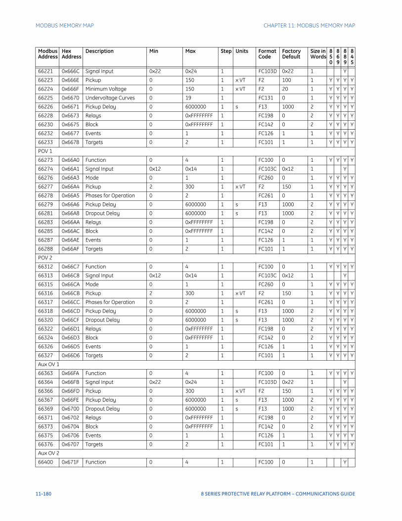
MODBUS MEMORY MAP CHAPTER 11: MODBUS MEMORY MAP
66221 0x666C Signal Input 0x22 0x24 1 FC103D 0x22 1 Y
66223 0x666E Pickup 0 150 1 x VT F2 100 1 Y Y Y Y
66224 0x666F Minimum Voltage 0 150 1 x VT F2 20 1 Y Y Y Y
66225 0x6670 Undervoltage Curves 0 19 1 FC131 0 1 Y Y Y Y
66226 0x6671 Pickup Delay 0 6000000 1 s F13 1000 2 Y Y Y Y
66228 0x6673 Relays 0 0xFFFFFFFF 1 FC198 0 2 Y Y Y Y
66230 0x6675 Block 0 0xFFFFFFFF 1 FC142 0 2 Y Y Y Y
66232 0x6677 Events 0 1 1 FC126 1 1 Y Y Y Y
66233 0x6678 Targets 0 2 1 FC101 1 1 Y Y Y Y
POV 1
66273 0x66A0 Function 0 4 1 FC100 0 1 Y Y Y Y
66274 0x66A1 Signal Input 0x12 0x14 1 FC103C 0x12 1 Y
66276 0x66A3 Mode 0 1 1 FC260 0 1 Y Y Y Y
66277 0x66A4 Pickup 2 300 1 x VT F2 150 1 Y Y Y Y
66278 0x66A5 Phases for Operation 0 2 1 FC261 0 1 Y Y Y Y
66279 0x66A6 Pickup Delay 0 6000000 1 s F13 1000 2 Y Y Y Y
66281 0x66A8 Dropout Delay 0 6000000 1 s F13 1000 2 Y Y Y Y
66283 0x66AA Relays 0 0xFFFFFFFF 1 FC198 0 2 Y Y Y Y
66285 0x66AC Block 0 0xFFFFFFFF 1 FC142 0 2 Y Y Y Y
66287 0x66AE Events 0 1 1 FC126 1 1 Y Y Y Y
66288 0x66AF Targets 0 2 1 FC101 1 1 Y Y Y Y
POV 2
66312 0x66C7 Function 0 4 1 FC100 0 1 Y Y Y Y
66313 0x66C8 Signal Input 0x12 0x14 1 FC103C 0x12 1 Y
66315 0x66CA Mode 0 1 1 FC260 0 1 Y Y Y Y
66316 0x66CB Pickup 2 300 1 x VT F2 150 1 Y Y Y Y
66317 0x66CC Phases for Operation 0 2 1 FC261 0 1 Y Y Y Y
66318 0x66CD Pickup Delay 0 6000000 1 s F13 1000 2 Y Y Y Y
66320 0x66CF Dropout Delay 0 6000000 1 s F13 1000 2 Y Y Y Y
66322 0x66D1 Relays 0 0xFFFFFFFF 1 FC198 0 2 Y Y Y Y
66324 0x66D3 Block 0 0xFFFFFFFF 1 FC142 0 2 Y Y Y Y
66326 0x66D5 Events 0 1 1 FC126 1 1 Y Y Y Y
66327 0x66D6 Targets 0 2 1 FC101 1 1 Y Y Y Y
Aux OV 1
66363 0x66FA Function 0 4 1 FC100 0 1 Y Y Y Y
66364 0x66FB Signal Input 0x22 0x24 1 FC103D 0x22 1 Y
66366 0x66FD Pickup 0 300 1 x VT F2 150 1 Y Y Y Y
66367 0x66FE Pickup Delay 0 6000000 1 s F13 1000 2 Y Y Y Y
66369 0x6700 Dropout Delay 0 6000000 1 s F13 1000 2 Y Y Y Y
66371 0x6702 Relays 0 0xFFFFFFFF 1 FC198 0 2 Y Y Y Y
66373 0x6704 Block 0 0xFFFFFFFF 1 FC142 0 2 Y Y Y Y
66375 0x6706 Events 0 1 1 FC126 1 1 Y Y Y Y
66376 0x6707 Targets 0 2 1 FC101 1 1 Y Y Y Y
Aux OV 2
66400 0x671F Function 0 4 1 FC100 0 1 Y
Modbus Address
Hex Address
Description Min Max Step Units Format Code
Factory Default
Size in Words
850
869
889
845
11-180 8 SERIES PROTECTIVE RELAY PLATFORM – COMMUNICATIONS GUIDE
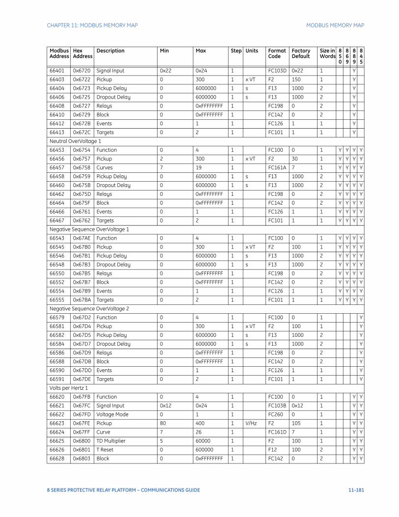
CHAPTER 11: MODBUS MEMORY MAP MODBUS MEMORY MAP
66401 0x6720 Signal Input 0x22 0x24 1 FC103D 0x22 1 Y
66403 0x6722 Pickup 0 300 1 x VT F2 150 1 Y
66404 0x6723 Pickup Delay 0 6000000 1 s F13 1000 2 Y
66406 0x6725 Dropout Delay 0 6000000 1 s F13 1000 2 Y
66408 0x6727 Relays 0 0xFFFFFFFF 1 FC198 0 2 Y
66410 0x6729 Block 0 0xFFFFFFFF 1 FC142 0 2 Y
66412 0x672B Events 0 1 1 FC126 1 1 Y
66413 0x672C Targets 0 2 1 FC101 1 1 Y
Neutral OverVoltage 1
66453 0x6754 Function 0 4 1 FC100 0 1 Y Y Y Y
66456 0x6757 Pickup 2 300 1 x VT F2 30 1 Y Y Y Y
66457 0x6758 Curves 7 19 1 FC161A 7 1 Y Y Y Y
66458 0x6759 Pickup Delay 0 6000000 1 s F13 1000 2 Y Y Y Y
66460 0x675B Dropout Delay 0 6000000 1 s F13 1000 2 Y Y Y Y
66462 0x675D Relays 0 0xFFFFFFFF 1 FC198 0 2 Y Y Y Y
66464 0x675F Block 0 0xFFFFFFFF 1 FC142 0 2 Y Y Y Y
66466 0x6761 Events 0 1 1 FC126 1 1 Y Y Y Y
66467 0x6762 Targets 0 2 1 FC101 1 1 Y Y Y Y
Negative Sequence OverVoltage 1
66543 0x67AE Function 0 4 1 FC100 0 1 Y Y Y Y
66545 0x67B0 Pickup 0 300 1 x VT F2 100 1 Y Y Y Y
66546 0x67B1 Pickup Delay 0 6000000 1 s F13 1000 2 Y Y Y Y
66548 0x67B3 Dropout Delay 0 6000000 1 s F13 1000 2 Y Y Y Y
66550 0x67B5 Relays 0 0xFFFFFFFF 1 FC198 0 2 Y Y Y Y
66552 0x67B7 Block 0 0xFFFFFFFF 1 FC142 0 2 Y Y Y Y
66554 0x67B9 Events 0 1 1 FC126 1 1 Y Y Y Y
66555 0x67BA Targets 0 2 1 FC101 1 1 Y Y Y Y
Negative Sequence OverVoltage 2
66579 0x67D2 Function 0 4 1 FC100 0 1 Y
66581 0x67D4 Pickup 0 300 1 x VT F2 100 1 Y
66582 0x67D5 Pickup Delay 0 6000000 1 s F13 1000 2 Y
66584 0x67D7 Dropout Delay 0 6000000 1 s F13 1000 2 Y
66586 0x67D9 Relays 0 0xFFFFFFFF 1 FC198 0 2 Y
66588 0x67DB Block 0 0xFFFFFFFF 1 FC142 0 2 Y
66590 0x67DD Events 0 1 1 FC126 1 1 Y
66591 0x67DE Targets 0 2 1 FC101 1 1 Y
Volts per Hertz 1
66620 0x67FB Function 0 4 1 FC100 0 1 Y Y
66621 0x67FC Signal Input 0x12 0x24 1 FC103B 0x12 1 Y Y
66622 0x67FD Voltage Mode 0 1 1 FC260 0 1 Y Y
66623 0x67FE Pickup 80 400 1 V/Hz F2 105 1 Y Y
66624 0x67FF Curve 7 26 1 FC161D 7 1 Y Y
66625 0x6800 TD Multiplier 5 60000 1 F2 100 1 Y Y
66626 0x6801 T Reset 0 600000 1 F12 100 2 Y Y
66628 0x6803 Block 0 0xFFFFFFFF 1 FC142 0 2 Y Y
Modbus Address
Hex Address
Description Min Max Step Units Format Code
Factory Default
Size in Words
850
869
889
845
8 SERIES PROTECTIVE RELAY PLATFORM – COMMUNICATIONS GUIDE 11-181
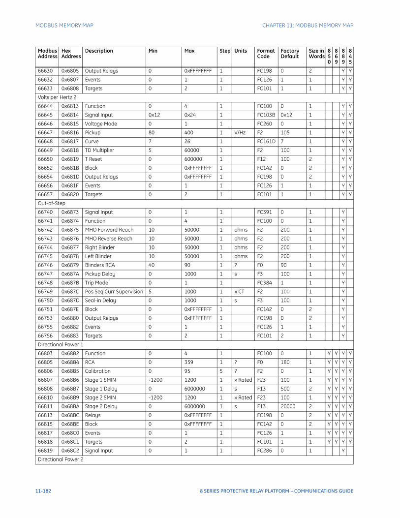
MODBUS MEMORY MAP CHAPTER 11: MODBUS MEMORY MAP
66630 0x6805 Output Relays 0 0xFFFFFFFF 1 FC198 0 2 Y Y
66632 0x6807 Events 0 1 1 FC126 1 1 Y Y
66633 0x6808 Targets 0 2 1 FC101 1 1 Y Y
Volts per Hertz 2
66644 0x6813 Function 0 4 1 FC100 0 1 Y Y
66645 0x6814 Signal Input 0x12 0x24 1 FC103B 0x12 1 Y Y
66646 0x6815 Voltage Mode 0 1 1 FC260 0 1 Y Y
66647 0x6816 Pickup 80 400 1 V/Hz F2 105 1 Y Y
66648 0x6817 Curve 7 26 1 FC161D 7 1 Y Y
66649 0x6818 TD Multiplier 5 60000 1 F2 100 1 Y Y
66650 0x6819 T Reset 0 600000 1 F12 100 2 Y Y
66652 0x681B Block 0 0xFFFFFFFF 1 FC142 0 2 Y Y
66654 0x681D Output Relays 0 0xFFFFFFFF 1 FC198 0 2 Y Y
66656 0x681F Events 0 1 1 FC126 1 1 Y Y
66657 0x6820 Targets 0 2 1 FC101 1 1 Y Y
Out-of-Step
66740 0x6873 Signal Input 0 1 1 FC391 0 1 Y
66741 0x6874 Function 0 4 1 FC100 0 1 Y
66742 0x6875 MHO Forward Reach 10 50000 1 ohms F2 200 1 Y
66743 0x6876 MHO Reverse Reach 10 50000 1 ohms F2 200 1 Y
66744 0x6877 Right Blinder 10 50000 1 ohms F2 200 1 Y
66745 0x6878 Left Blinder 10 50000 1 ohms F2 200 1 Y
66746 0x6879 Blinders RCA 40 90 1 ? F0 90 1 Y
66747 0x687A Pickup Delay 0 1000 1 s F3 100 1 Y
66748 0x687B Trip Mode 0 1 1 FC384 1 1 Y
66749 0x687C Pos Seq Curr Supervision 5 1000 1 x CT F2 100 1 Y
66750 0x687D Seal-in Delay 0 1000 1 s F3 100 1 Y
66751 0x687E Block 0 0xFFFFFFFF 1 FC142 0 2 Y
66753 0x6880 Output Relays 0 0xFFFFFFFF 1 FC198 0 2 Y
66755 0x6882 Events 0 1 1 FC126 1 1 Y
66756 0x6883 Targets 0 2 1 FC101 2 1 Y
Directional Power 1
66803 0x68B2 Function 0 4 1 FC100 0 1 Y Y Y Y
66805 0x68B4 RCA 0 359 1 ? F0 180 1 Y Y Y Y
66806 0x68B5 Calibration 0 95 5 ? F2 0 1 Y Y Y Y
66807 0x68B6 Stage 1 SMIN -1200 1200 1 x Rated F23 100 1 Y Y Y Y
66808 0x68B7 Stage 1 Delay 0 6000000 1 s F13 500 2 Y Y Y Y
66810 0x68B9 Stage 2 SMIN -1200 1200 1 x Rated F23 100 1 Y Y Y Y
66811 0x68BA Stage 2 Delay 0 6000000 1 s F13 20000 2 Y Y Y Y
66813 0x68BC Relays 0 0xFFFFFFFF 1 FC198 0 2 Y Y Y Y
66815 0x68BE Block 0 0xFFFFFFFF 1 FC142 0 2 Y Y Y Y
66817 0x68C0 Events 0 1 1 FC126 1 1 Y Y Y Y
66818 0x68C1 Targets 0 2 1 FC101 1 1 Y Y Y Y
66819 0x68C2 Signal Input 0 1 1 FC286 0 1 Y
Directional Power 2
Modbus Address
Hex Address
Description Min Max Step Units Format Code
Factory Default
Size in Words
850
869
889
845
11-182 8 SERIES PROTECTIVE RELAY PLATFORM – COMMUNICATIONS GUIDE
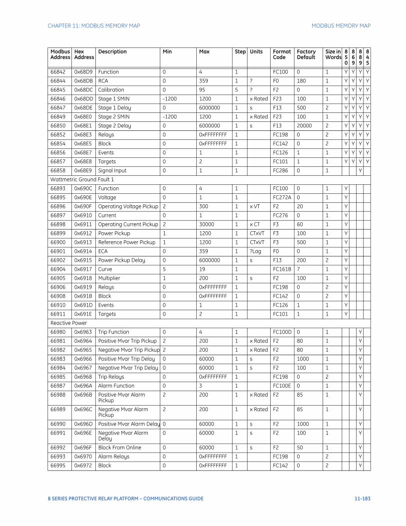
CHAPTER 11: MODBUS MEMORY MAP MODBUS MEMORY MAP
66842 0x68D9 Function 0 4 1 FC100 0 1 Y Y Y Y
66844 0x68DB RCA 0 359 1 ? F0 180 1 Y Y Y Y
66845 0x68DC Calibration 0 95 5 ? F2 0 1 Y Y Y Y
66846 0x68DD Stage 1 SMIN -1200 1200 1 x Rated F23 100 1 Y Y Y Y
66847 0x68DE Stage 1 Delay 0 6000000 1 s F13 500 2 Y Y Y Y
66849 0x68E0 Stage 2 SMIN -1200 1200 1 x Rated F23 100 1 Y Y Y Y
66850 0x68E1 Stage 2 Delay 0 6000000 1 s F13 20000 2 Y Y Y Y
66852 0x68E3 Relays 0 0xFFFFFFFF 1 FC198 0 2 Y Y Y Y
66854 0x68E5 Block 0 0xFFFFFFFF 1 FC142 0 2 Y Y Y Y
66856 0x68E7 Events 0 1 1 FC126 1 1 Y Y Y Y
66857 0x68E8 Targets 0 2 1 FC101 1 1 Y Y Y Y
66858 0x68E9 Signal Input 0 1 1 FC286 0 1 Y
Wattmetric Ground Fault 1
66893 0x690C Function 0 4 1 FC100 0 1 Y
66895 0x690E Voltage 0 1 1 FC272A 0 1 Y
66896 0x690F Operating Voltage Pickup 2 300 1 x VT F2 20 1 Y
66897 0x6910 Current 0 1 1 FC276 0 1 Y
66898 0x6911 Operating Current Pickup 2 30000 1 x CT F3 60 1 Y
66899 0x6912 Power Pickup 1 1200 1 CTxVT F3 100 1 Y
66900 0x6913 Reference Power Pickup 1 1200 1 CTxVT F3 500 1 Y
66901 0x6914 ECA 0 359 1 ?Lag F0 0 1 Y
66902 0x6915 Power Pickup Delay 0 6000000 1 s F13 200 2 Y
66904 0x6917 Curve 5 19 1 FC161B 7 1 Y
66905 0x6918 Multiplier 1 200 1 s F2 100 1 Y
66906 0x6919 Relays 0 0xFFFFFFFF 1 FC198 0 2 Y
66908 0x691B Block 0 0xFFFFFFFF 1 FC142 0 2 Y
66910 0x691D Events 0 1 1 FC126 1 1 Y
66911 0x691E Targets 0 2 1 FC101 1 1 Y
Reactive Power
66980 0x6963 Trip Function 0 4 1 FC100D 0 1 Y
66981 0x6964 Positive Mvar Trip Pickup 2 200 1 x Rated F2 80 1 Y
66982 0x6965 Negative Mvar Trip Pickup 2 200 1 x Rated F2 80 1 Y
66983 0x6966 Positive Mvar Trip Delay 0 60000 1 s F2 1000 1 Y
66984 0x6967 Negative Mvar Trip Delay 0 60000 1 s F2 100 1 Y
66985 0x6968 Trip Relays 0 0xFFFFFFFF 1 FC198 0 2 Y
66987 0x696A Alarm Function 0 3 1 FC100E 0 1 Y
66988 0x696B Positive Mvar Alarm Pickup
2 200 1 x Rated F2 85 1 Y
66989 0x696C Negative Mvar Alarm Pickup
2 200 1 x Rated F2 85 1 Y
66990 0x696D Positive Mvar Alarm Delay 0 60000 1 s F2 1000 1 Y
66991 0x696E Negative Mvar Alarm Delay
0 60000 1 s F2 100 1 Y
66992 0x696F Block From Online 0 60000 1 s F2 50 1 Y
66993 0x6970 Alarm Relays 0 0xFFFFFFFF 1 FC198 0 2 Y
66995 0x6972 Block 0 0xFFFFFFFF 1 FC142 0 2 Y
Modbus Address
Hex Address
Description Min Max Step Units Format Code
Factory Default
Size in Words
850
869
889
845
8 SERIES PROTECTIVE RELAY PLATFORM – COMMUNICATIONS GUIDE 11-183
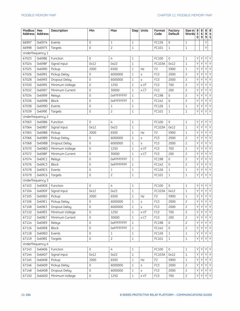
MODBUS MEMORY MAP CHAPTER 11: MODBUS MEMORY MAP
66997 0x6974 Events 0 1 1 FC126 0 1 Y
66998 0x6975 Targets 0 2 1 FC101 1 1 Y
Underfrequency 1
67023 0x698E Function 0 4 1 FC100 0 1 Y Y Y Y
67024 0x698F Signal Input 0x12 0x22 1 FC103A 0x12 1 Y Y Y Y
67025 0x6990 Pickup 2000 6500 1 Hz F2 5900 1 Y Y Y Y
67026 0x6991 Pickup Delay 0 6000000 1 s F13 2000 2 Y Y Y Y
67028 0x6993 Dropout Delay 0 6000000 1 s F13 2000 2 Y Y Y Y
67030 0x6995 Minimum Voltage 0 1250 1 x VT F13 700 2 Y Y Y Y
67032 0x6997 Minimum Current 0 30000 1 x CT F13 200 2 Y Y Y Y
67034 0x6999 Relays 0 0xFFFFFFFF 1 FC198 0 2 Y Y Y Y
67036 0x699B Block 0 0xFFFFFFFF 1 FC142 0 2 Y Y Y Y
67038 0x699D Events 0 1 1 FC126 1 1 Y Y Y Y
67039 0x699E Targets 0 2 1 FC101 1 1 Y Y Y Y
Underfrequency 2
67063 0x69B6 Function 0 4 1 FC100 0 1 Y Y Y Y
67064 0x69B7 Signal Input 0x12 0x22 1 FC103A 0x12 1 Y Y Y Y
67065 0x69B8 Pickup 2000 6500 1 Hz F2 5900 1 Y Y Y Y
67066 0x69B9 Pickup Delay 0 6000000 1 s F13 2000 2 Y Y Y Y
67068 0x69BB Dropout Delay 0 6000000 1 s F13 2000 2 Y Y Y Y
67070 0x69BD Minimum Voltage 0 1250 1 x VT F13 700 2 Y Y Y Y
67072 0x69BF Minimum Current 0 30000 1 x CT F13 200 2 Y Y Y Y
67074 0x69C1 Relays 0 0xFFFFFFFF 1 FC198 0 2 Y Y Y Y
67076 0x69C3 Block 0 0xFFFFFFFF 1 FC142 0 2 Y Y Y Y
67078 0x69C5 Events 0 1 1 FC126 1 1 Y Y Y Y
67079 0x69C6 Targets 0 2 1 FC101 1 1 Y Y Y Y
Underfrequency 3
67103 0x69DE Function 0 4 1 FC100 0 1 Y Y Y Y
67104 0x69DF Signal Input 0x12 0x22 1 FC103A 0x12 1 Y Y Y Y
67105 0x69E0 Pickup 2000 6500 1 Hz F2 5900 1 Y Y Y Y
67106 0x69E1 Pickup Delay 0 6000000 1 s F13 2000 2 Y Y Y Y
67108 0x69E3 Dropout Delay 0 6000000 1 s F13 2000 2 Y Y Y Y
67110 0x69E5 Minimum Voltage 0 1250 1 x VT F13 700 2 Y Y Y Y
67112 0x69E7 Minimum Current 0 30000 1 x CT F13 200 2 Y Y Y Y
67114 0x69E9 Relays 0 0xFFFFFFFF 1 FC198 0 2 Y Y Y Y
67116 0x69EB Block 0 0xFFFFFFFF 1 FC142 0 2 Y Y Y Y
67118 0x69ED Events 0 1 1 FC126 1 1 Y Y Y Y
67119 0x69EE Targets 0 2 1 FC101 1 1 Y Y Y Y
Underfrequency 4
67143 0x6A06 Function 0 4 1 FC100 0 1 Y Y Y Y
67144 0x6A07 Signal Input 0x12 0x22 1 FC103A 0x12 1 Y Y Y Y
67145 0x6A08 Pickup 2000 6500 1 Hz F2 5900 1 Y Y Y Y
67146 0x6A09 Pickup Delay 0 6000000 1 s F13 2000 2 Y Y Y Y
67148 0x6A0B Dropout Delay 0 6000000 1 s F13 2000 2 Y Y Y Y
67150 0x6A0D Minimum Voltage 0 1250 1 x VT F13 700 2 Y Y Y Y
Modbus Address
Hex Address
Description Min Max Step Units Format Code
Factory Default
Size in Words
850
869
889
845
11-184 8 SERIES PROTECTIVE RELAY PLATFORM – COMMUNICATIONS GUIDE

CHAPTER 11: MODBUS MEMORY MAP MODBUS MEMORY MAP
67152 0x6A0F Minimum Current 0 30000 1 x CT F13 200 2 Y Y Y Y
67154 0x6A11 Relays 0 0xFFFFFFFF 1 FC198 0 2 Y Y Y Y
67156 0x6A13 Block 0 0xFFFFFFFF 1 FC142 0 2 Y Y Y Y
67158 0x6A15 Events 0 1 1 FC126 1 1 Y Y Y Y
67159 0x6A16 Targets 0 2 1 FC101 1 1 Y Y Y Y
Underfrequency 5
67183 0x6A2E Function 0 4 1 FC100 0 1 Y
67184 0x6A2F Signal Input 0x12 0x22 1 FC103A 0x12 1 Y
67185 0x6A30 Pickup 2000 6500 1 Hz F2 5900 1 Y
67186 0x6A31 Pickup Delay 0 6000000 1 s F13 2000 2 Y
67188 0x6A33 Dropout Delay 0 6000000 1 s F13 2000 2 Y
67190 0x6A35 Minimum Voltage 0 1250 1 x VT F13 700 2 Y
67192 0x6A37 Minimum Current 0 30000 1 x CT F13 200 2 Y
67194 0x6A39 Relays 0 0xFFFFFFFF 1 FC198 0 2 Y
67196 0x6A3B Block 0 0xFFFFFFFF 1 FC142 0 2 Y
67198 0x6A3D Events 0 1 1 FC126 1 1 Y
67199 0x6A3E Targets 0 2 1 FC101 1 1 Y
Underfrequency 6
67223 0x6A56 Function 0 4 1 FC100 0 1 Y
67224 0x6A57 Signal Input 0x12 0x22 1 FC103A 0x12 1 Y
67225 0x6A58 Pickup 2000 6500 1 Hz F2 5900 1 Y
67226 0x6A59 Pickup Delay 0 6000000 1 s F13 2000 2 Y
67228 0x6A5B Dropout Delay 0 6000000 1 s F13 2000 2 Y
67230 0x6A5D Minimum Voltage 0 1250 1 x VT F13 700 2 Y
67232 0x6A5F Minimum Current 0 30000 1 x CT F13 200 2 Y
67234 0x6A61 Relays 0 0xFFFFFFFF 1 FC198 0 2 Y
67236 0x6A63 Block 0 0xFFFFFFFF 1 FC142 0 2 Y
67238 0x6A65 Events 0 1 1 FC126 1 1 Y
67239 0x6A66 Targets 0 2 1 FC101 1 1 Y
Overfrequency 1
67273 0x6A88 Function 0 4 1 FC100 0 1 Y Y Y Y
67274 0x6A89 Signal Input 0x12 0x22 1 FC103A 0x12 1 Y Y Y Y
67275 0x6A8A Pickup 2000 6500 1 Hz F2 6050 1 Y Y Y Y
67276 0x6A8B Pickup Delay 0 6000000 1 s F13 5000 2 Y Y Y Y
67278 0x6A8D Dropout Delay 0 6000000 1 s F13 5000 2 Y Y Y Y
67280 0x6A8F Minimum Voltage 0 1250 1 x VT F13 300 2 Y Y Y Y
67282 0x6A91 Relays 0 0xFFFFFFFF 1 FC198 0 2 Y Y Y Y
67284 0x6A93 Block 0 0xFFFFFFFF 1 FC142 0 2 Y Y Y Y
67286 0x6A95 Events 0 1 1 FC126 1 1 Y Y Y Y
67287 0x6A96 Targets 0 2 1 FC101 1 1 Y Y Y Y
Overfrequency 2
67311 0x6AAE Function 0 4 1 FC100 0 1 Y Y Y Y
67312 0x6AAF Signal Input 0x12 0x22 1 FC103A 0x12 1 Y Y Y Y
67313 0x6AB0 Pickup 2000 6500 1 Hz F2 6050 1 Y Y Y Y
67314 0x6AB1 Pickup Delay 0 6000000 1 s F13 5000 2 Y Y Y Y
Modbus Address
Hex Address
Description Min Max Step Units Format Code
Factory Default
Size in Words
850
869
889
845
8 SERIES PROTECTIVE RELAY PLATFORM – COMMUNICATIONS GUIDE 11-185
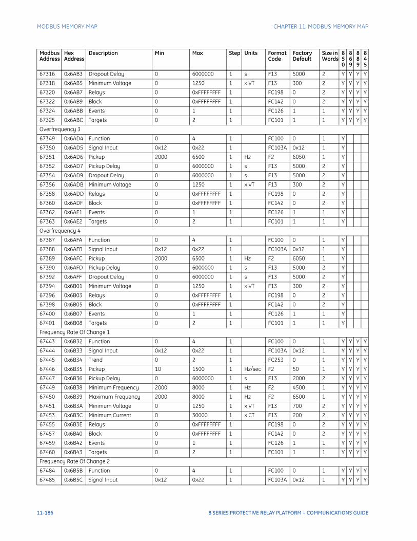
MODBUS MEMORY MAP CHAPTER 11: MODBUS MEMORY MAP
67316 0x6AB3 Dropout Delay 0 6000000 1 s F13 5000 2 Y Y Y Y
67318 0x6AB5 Minimum Voltage 0 1250 1 x VT F13 300 2 Y Y Y Y
67320 0x6AB7 Relays 0 0xFFFFFFFF 1 FC198 0 2 Y Y Y Y
67322 0x6AB9 Block 0 0xFFFFFFFF 1 FC142 0 2 Y Y Y Y
67324 0x6ABB Events 0 1 1 FC126 1 1 Y Y Y Y
67325 0x6ABC Targets 0 2 1 FC101 1 1 Y Y Y Y
Overfrequency 3
67349 0x6AD4 Function 0 4 1 FC100 0 1 Y
67350 0x6AD5 Signal Input 0x12 0x22 1 FC103A 0x12 1 Y
67351 0x6AD6 Pickup 2000 6500 1 Hz F2 6050 1 Y
67352 0x6AD7 Pickup Delay 0 6000000 1 s F13 5000 2 Y
67354 0x6AD9 Dropout Delay 0 6000000 1 s F13 5000 2 Y
67356 0x6ADB Minimum Voltage 0 1250 1 x VT F13 300 2 Y
67358 0x6ADD Relays 0 0xFFFFFFFF 1 FC198 0 2 Y
67360 0x6ADF Block 0 0xFFFFFFFF 1 FC142 0 2 Y
67362 0x6AE1 Events 0 1 1 FC126 1 1 Y
67363 0x6AE2 Targets 0 2 1 FC101 1 1 Y
Overfrequency 4
67387 0x6AFA Function 0 4 1 FC100 0 1 Y
67388 0x6AFB Signal Input 0x12 0x22 1 FC103A 0x12 1 Y
67389 0x6AFC Pickup 2000 6500 1 Hz F2 6050 1 Y
67390 0x6AFD Pickup Delay 0 6000000 1 s F13 5000 2 Y
67392 0x6AFF Dropout Delay 0 6000000 1 s F13 5000 2 Y
67394 0x6B01 Minimum Voltage 0 1250 1 x VT F13 300 2 Y
67396 0x6B03 Relays 0 0xFFFFFFFF 1 FC198 0 2 Y
67398 0x6B05 Block 0 0xFFFFFFFF 1 FC142 0 2 Y
67400 0x6B07 Events 0 1 1 FC126 1 1 Y
67401 0x6B08 Targets 0 2 1 FC101 1 1 Y
Frequency Rate Of Change 1
67443 0x6B32 Function 0 4 1 FC100 0 1 Y Y Y Y
67444 0x6B33 Signal Input 0x12 0x22 1 FC103A 0x12 1 Y Y Y Y
67445 0x6B34 Trend 0 2 1 FC253 0 1 Y Y Y Y
67446 0x6B35 Pickup 10 1500 1 Hz/sec F2 50 1 Y Y Y Y
67447 0x6B36 Pickup Delay 0 6000000 1 s F13 2000 2 Y Y Y Y
67449 0x6B38 Minimum Frequency 2000 8000 1 Hz F2 4500 1 Y Y Y Y
67450 0x6B39 Maximum Frequency 2000 8000 1 Hz F2 6500 1 Y Y Y Y
67451 0x6B3A Minimum Voltage 0 1250 1 x VT F13 700 2 Y Y Y Y
67453 0x6B3C Minimum Current 0 30000 1 x CT F13 200 2 Y Y Y Y
67455 0x6B3E Relays 0 0xFFFFFFFF 1 FC198 0 2 Y Y Y Y
67457 0x6B40 Block 0 0xFFFFFFFF 1 FC142 0 2 Y Y Y Y
67459 0x6B42 Events 0 1 1 FC126 1 1 Y Y Y Y
67460 0x6B43 Targets 0 2 1 FC101 1 1 Y Y Y Y
Frequency Rate Of Change 2
67484 0x6B5B Function 0 4 1 FC100 0 1 Y Y Y Y
67485 0x6B5C Signal Input 0x12 0x22 1 FC103A 0x12 1 Y Y Y Y
Modbus Address
Hex Address
Description Min Max Step Units Format Code
Factory Default
Size in Words
850
869
889
845
11-186 8 SERIES PROTECTIVE RELAY PLATFORM – COMMUNICATIONS GUIDE
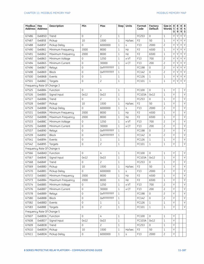
CHAPTER 11: MODBUS MEMORY MAP MODBUS MEMORY MAP
67486 0x6B5D Trend 0 2 1 FC253 0 1 Y Y Y Y
67487 0x6B5E Pickup 10 1500 1 Hz/sec F2 50 1 Y Y Y Y
67488 0x6B5F Pickup Delay 0 6000000 1 s F13 2000 2 Y Y Y Y
67490 0x6B61 Minimum Frequency 2000 8000 1 Hz F2 4500 1 Y Y Y Y
67491 0x6B62 Maximum Frequency 2000 8000 1 Hz F2 6500 1 Y Y Y Y
67492 0x6B63 Minimum Voltage 0 1250 1 x VT F13 700 2 Y Y Y Y
67494 0x6B65 Minimum Current 0 30000 1 x CT F13 200 2 Y Y Y Y
67496 0x6B67 Relays 0 0xFFFFFFFF 1 FC198 0 2 Y Y Y Y
67498 0x6B69 Block 0 0xFFFFFFFF 1 FC142 0 2 Y Y Y Y
67500 0x6B6B Events 0 1 1 FC126 1 1 Y Y Y Y
67501 0x6B6C Targets 0 2 1 FC101 1 1 Y Y Y Y
Frequency Rate Of Change 3
67525 0x6B84 Function 0 4 1 FC100 0 1 Y Y
67526 0x6B85 Signal Input 0x12 0x22 1 FC103A 0x12 1 Y Y
67527 0x6B86 Trend 0 2 1 FC253 0 1 Y Y
67528 0x6B87 Pickup 10 1500 1 Hz/sec F2 50 1 Y Y
67529 0x6B88 Pickup Delay 0 6000000 1 s F13 2000 2 Y Y
67531 0x6B8A Minimum Frequency 2000 8000 1 Hz F2 4500 1 Y Y
67532 0x6B8B Maximum Frequency 2000 8000 1 Hz F2 6500 1 Y Y
67533 0x6B8C Minimum Voltage 0 1250 1 x VT F13 700 2 Y Y
67535 0x6B8E Minimum Current 0 30000 1 x CT F13 200 2 Y Y
67537 0x6B90 Relays 0 0xFFFFFFFF 1 FC198 0 2 Y Y
67539 0x6B92 Block 0 0xFFFFFFFF 1 FC142 0 2 Y Y
67541 0x6B94 Events 0 1 1 FC126 1 1 Y Y
67542 0x6B95 Targets 0 2 1 FC101 1 1 Y Y
Frequency Rate Of Change 4
67566 0x6BAD Function 0 4 1 FC100 0 1 Y Y
67567 0x6BAE Signal Input 0x12 0x22 1 FC103A 0x12 1 Y Y
67568 0x6BAF Trend 0 2 1 FC253 0 1 Y Y
67569 0x6BB0 Pickup 10 1500 1 Hz/sec F2 50 1 Y Y
67570 0x6BB1 Pickup Delay 0 6000000 1 s F13 2000 2 Y Y
67572 0x6BB3 Minimum Frequency 2000 8000 1 Hz F2 4500 1 Y Y
67573 0x6BB4 Maximum Frequency 2000 8000 1 Hz F2 6500 1 Y Y
67574 0x6BB5 Minimum Voltage 0 1250 1 x VT F13 700 2 Y Y
67576 0x6BB7 Minimum Current 0 30000 1 x CT F13 200 2 Y Y
67578 0x6BB9 Relays 0 0xFFFFFFFF 1 FC198 0 2 Y Y
67580 0x6BBB Block 0 0xFFFFFFFF 1 FC142 0 2 Y Y
67582 0x6BBD Events 0 1 1 FC126 1 1 Y Y
67583 0x6BBE Targets 0 2 1 FC101 1 1 Y Y
Frequency Rate Of Change 5
67607 0x6BD6 Function 0 4 1 FC100 0 1 Y
67608 0x6BD7 Signal Input 0x12 0x22 1 FC103A 0x12 1 Y
67609 0x6BD8 Trend 0 2 1 FC253 0 1 Y
67610 0x6BD9 Pickup 10 1500 1 Hz/sec F2 50 1 Y
67611 0x6BDA Pickup Delay 0 6000000 1 s F13 2000 2 Y
Modbus Address
Hex Address
Description Min Max Step Units Format Code
Factory Default
Size in Words
850
869
889
845
8 SERIES PROTECTIVE RELAY PLATFORM – COMMUNICATIONS GUIDE 11-187
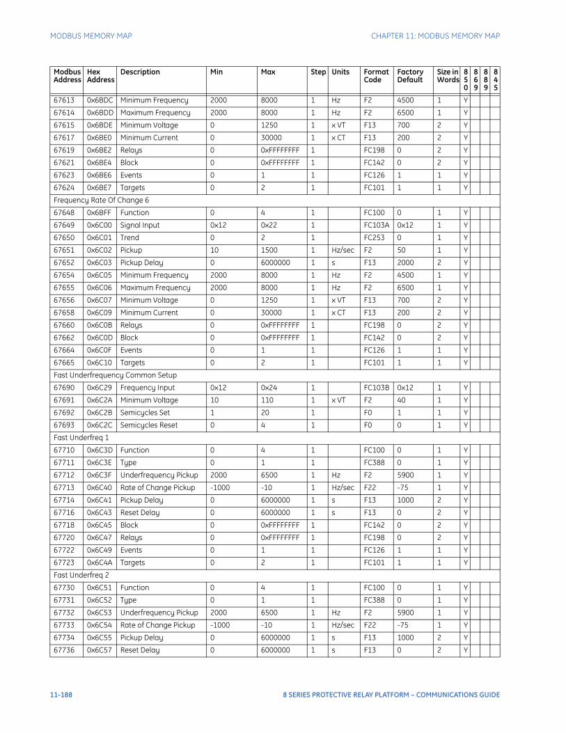
MODBUS MEMORY MAP CHAPTER 11: MODBUS MEMORY MAP
67613 0x6BDC Minimum Frequency 2000 8000 1 Hz F2 4500 1 Y
67614 0x6BDD Maximum Frequency 2000 8000 1 Hz F2 6500 1 Y
67615 0x6BDE Minimum Voltage 0 1250 1 x VT F13 700 2 Y
67617 0x6BE0 Minimum Current 0 30000 1 x CT F13 200 2 Y
67619 0x6BE2 Relays 0 0xFFFFFFFF 1 FC198 0 2 Y
67621 0x6BE4 Block 0 0xFFFFFFFF 1 FC142 0 2 Y
67623 0x6BE6 Events 0 1 1 FC126 1 1 Y
67624 0x6BE7 Targets 0 2 1 FC101 1 1 Y
Frequency Rate Of Change 6
67648 0x6BFF Function 0 4 1 FC100 0 1 Y
67649 0x6C00 Signal Input 0x12 0x22 1 FC103A 0x12 1 Y
67650 0x6C01 Trend 0 2 1 FC253 0 1 Y
67651 0x6C02 Pickup 10 1500 1 Hz/sec F2 50 1 Y
67652 0x6C03 Pickup Delay 0 6000000 1 s F13 2000 2 Y
67654 0x6C05 Minimum Frequency 2000 8000 1 Hz F2 4500 1 Y
67655 0x6C06 Maximum Frequency 2000 8000 1 Hz F2 6500 1 Y
67656 0x6C07 Minimum Voltage 0 1250 1 x VT F13 700 2 Y
67658 0x6C09 Minimum Current 0 30000 1 x CT F13 200 2 Y
67660 0x6C0B Relays 0 0xFFFFFFFF 1 FC198 0 2 Y
67662 0x6C0D Block 0 0xFFFFFFFF 1 FC142 0 2 Y
67664 0x6C0F Events 0 1 1 FC126 1 1 Y
67665 0x6C10 Targets 0 2 1 FC101 1 1 Y
Fast Underfrequency Common Setup
67690 0x6C29 Frequency Input 0x12 0x24 1 FC103B 0x12 1 Y
67691 0x6C2A Minimum Voltage 10 110 1 x VT F2 40 1 Y
67692 0x6C2B Semicycles Set 1 20 1 F0 1 1 Y
67693 0x6C2C Semicycles Reset 0 4 1 F0 0 1 Y
Fast Underfreq 1
67710 0x6C3D Function 0 4 1 FC100 0 1 Y
67711 0x6C3E Type 0 1 1 FC388 0 1 Y
67712 0x6C3F Underfrequency Pickup 2000 6500 1 Hz F2 5900 1 Y
67713 0x6C40 Rate of Change Pickup -1000 -10 1 Hz/sec F22 -75 1 Y
67714 0x6C41 Pickup Delay 0 6000000 1 s F13 1000 2 Y
67716 0x6C43 Reset Delay 0 6000000 1 s F13 0 2 Y
67718 0x6C45 Block 0 0xFFFFFFFF 1 FC142 0 2 Y
67720 0x6C47 Relays 0 0xFFFFFFFF 1 FC198 0 2 Y
67722 0x6C49 Events 0 1 1 FC126 1 1 Y
67723 0x6C4A Targets 0 2 1 FC101 1 1 Y
Fast Underfreq 2
67730 0x6C51 Function 0 4 1 FC100 0 1 Y
67731 0x6C52 Type 0 1 1 FC388 0 1 Y
67732 0x6C53 Underfrequency Pickup 2000 6500 1 Hz F2 5900 1 Y
67733 0x6C54 Rate of Change Pickup -1000 -10 1 Hz/sec F22 -75 1 Y
67734 0x6C55 Pickup Delay 0 6000000 1 s F13 1000 2 Y
67736 0x6C57 Reset Delay 0 6000000 1 s F13 0 2 Y
Modbus Address
Hex Address
Description Min Max Step Units Format Code
Factory Default
Size in Words
850
869
889
845
11-188 8 SERIES PROTECTIVE RELAY PLATFORM – COMMUNICATIONS GUIDE
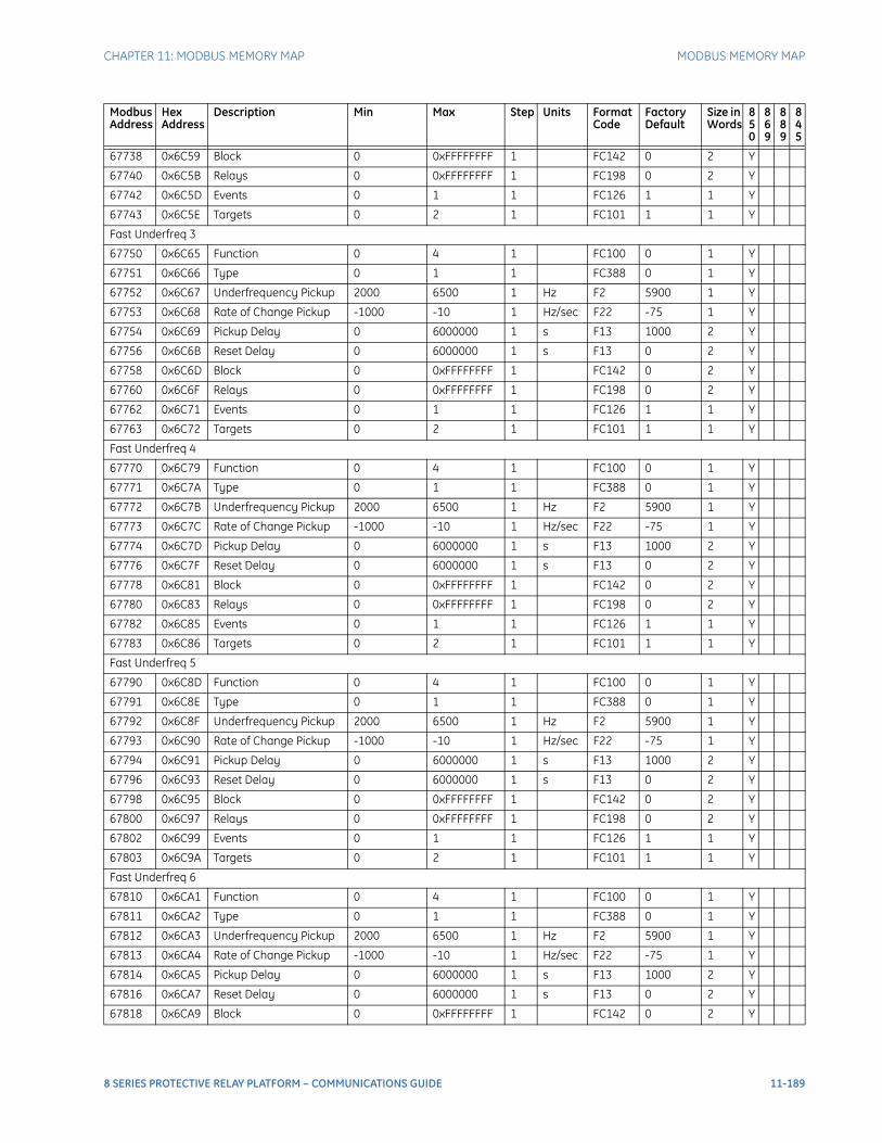
CHAPTER 11: MODBUS MEMORY MAP MODBUS MEMORY MAP
67738 0x6C59 Block 0 0xFFFFFFFF 1 FC142 0 2 Y
67740 0x6C5B Relays 0 0xFFFFFFFF 1 FC198 0 2 Y
67742 0x6C5D Events 0 1 1 FC126 1 1 Y
67743 0x6C5E Targets 0 2 1 FC101 1 1 Y
Fast Underfreq 3
67750 0x6C65 Function 0 4 1 FC100 0 1 Y
67751 0x6C66 Type 0 1 1 FC388 0 1 Y
67752 0x6C67 Underfrequency Pickup 2000 6500 1 Hz F2 5900 1 Y
67753 0x6C68 Rate of Change Pickup -1000 -10 1 Hz/sec F22 -75 1 Y
67754 0x6C69 Pickup Delay 0 6000000 1 s F13 1000 2 Y
67756 0x6C6B Reset Delay 0 6000000 1 s F13 0 2 Y
67758 0x6C6D Block 0 0xFFFFFFFF 1 FC142 0 2 Y
67760 0x6C6F Relays 0 0xFFFFFFFF 1 FC198 0 2 Y
67762 0x6C71 Events 0 1 1 FC126 1 1 Y
67763 0x6C72 Targets 0 2 1 FC101 1 1 Y
Fast Underfreq 4
67770 0x6C79 Function 0 4 1 FC100 0 1 Y
67771 0x6C7A Type 0 1 1 FC388 0 1 Y
67772 0x6C7B Underfrequency Pickup 2000 6500 1 Hz F2 5900 1 Y
67773 0x6C7C Rate of Change Pickup -1000 -10 1 Hz/sec F22 -75 1 Y
67774 0x6C7D Pickup Delay 0 6000000 1 s F13 1000 2 Y
67776 0x6C7F Reset Delay 0 6000000 1 s F13 0 2 Y
67778 0x6C81 Block 0 0xFFFFFFFF 1 FC142 0 2 Y
67780 0x6C83 Relays 0 0xFFFFFFFF 1 FC198 0 2 Y
67782 0x6C85 Events 0 1 1 FC126 1 1 Y
67783 0x6C86 Targets 0 2 1 FC101 1 1 Y
Fast Underfreq 5
67790 0x6C8D Function 0 4 1 FC100 0 1 Y
67791 0x6C8E Type 0 1 1 FC388 0 1 Y
67792 0x6C8F Underfrequency Pickup 2000 6500 1 Hz F2 5900 1 Y
67793 0x6C90 Rate of Change Pickup -1000 -10 1 Hz/sec F22 -75 1 Y
67794 0x6C91 Pickup Delay 0 6000000 1 s F13 1000 2 Y
67796 0x6C93 Reset Delay 0 6000000 1 s F13 0 2 Y
67798 0x6C95 Block 0 0xFFFFFFFF 1 FC142 0 2 Y
67800 0x6C97 Relays 0 0xFFFFFFFF 1 FC198 0 2 Y
67802 0x6C99 Events 0 1 1 FC126 1 1 Y
67803 0x6C9A Targets 0 2 1 FC101 1 1 Y
Fast Underfreq 6
67810 0x6CA1 Function 0 4 1 FC100 0 1 Y
67811 0x6CA2 Type 0 1 1 FC388 0 1 Y
67812 0x6CA3 Underfrequency Pickup 2000 6500 1 Hz F2 5900 1 Y
67813 0x6CA4 Rate of Change Pickup -1000 -10 1 Hz/sec F22 -75 1 Y
67814 0x6CA5 Pickup Delay 0 6000000 1 s F13 1000 2 Y
67816 0x6CA7 Reset Delay 0 6000000 1 s F13 0 2 Y
67818 0x6CA9 Block 0 0xFFFFFFFF 1 FC142 0 2 Y
Modbus Address
Hex Address
Description Min Max Step Units Format Code
Factory Default
Size in Words
850
869
889
845
8 SERIES PROTECTIVE RELAY PLATFORM – COMMUNICATIONS GUIDE 11-189
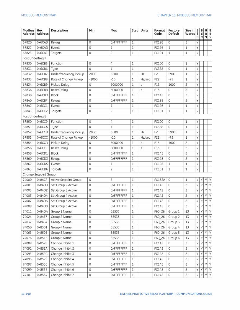
MODBUS MEMORY MAP CHAPTER 11: MODBUS MEMORY MAP
67820 0x6CAB Relays 0 0xFFFFFFFF 1 FC198 0 2 Y
67822 0x6CAD Events 0 1 1 FC126 1 1 Y
67823 0x6CAE Targets 0 2 1 FC101 1 1 Y
Fast Underfreq 7
67830 0x6CB5 Function 0 4 1 FC100 0 1 Y
67831 0x6CB6 Type 0 1 1 FC388 0 1 Y
67832 0x6CB7 Underfrequency Pickup 2000 6500 1 Hz F2 5900 1 Y
67833 0x6CB8 Rate of Change Pickup -1000 -10 1 Hz/sec F22 -75 1 Y
67834 0x6CB9 Pickup Delay 0 6000000 1 s F13 1000 2 Y
67836 0x6CBB Reset Delay 0 6000000 1 s F13 0 2 Y
67838 0x6CBD Block 0 0xFFFFFFFF 1 FC142 0 2 Y
67840 0x6CBF Relays 0 0xFFFFFFFF 1 FC198 0 2 Y
67842 0x6CC1 Events 0 1 1 FC126 1 1 Y
67843 0x6CC2 Targets 0 2 1 FC101 1 1 Y
Fast Underfreq 8
67850 0x6CC9 Function 0 4 1 FC100 0 1 Y
67851 0x6CCA Type 0 1 1 FC388 0 1 Y
67852 0x6CCB Underfrequency Pickup 2000 6500 1 Hz F2 5900 1 Y
67853 0x6CCC Rate of Change Pickup -1000 -10 1 Hz/sec F22 -75 1 Y
67854 0x6CCD Pickup Delay 0 6000000 1 s F13 1000 2 Y
67856 0x6CCF Reset Delay 0 6000000 1 s F13 0 2 Y
67858 0x6CD1 Block 0 0xFFFFFFFF 1 FC142 0 2 Y
67860 0x6CD3 Relays 0 0xFFFFFFFF 1 FC198 0 2 Y
67862 0x6CD5 Events 0 1 1 FC126 1 1 Y
67863 0x6CD6 Targets 0 2 1 FC101 1 1 Y
Change Setpoint Group
74000 0x84CF Active Setpoint Group 0 5 1 FC132A 0 1 Y Y Y Y
74001 0x84D0 Set Group 2 Active 0 0xFFFFFFFF 1 FC142 0 2 Y Y Y Y
74003 0x84D2 Set Group 3 Active 0 0xFFFFFFFF 1 FC142 0 2 Y Y Y Y
74005 0x84D4 Set Group 4 Active 0 0xFFFFFFFF 1 FC142 0 2 Y Y Y Y
74007 0x84D6 Set Group 5 Active 0 0xFFFFFFFF 1 FC142 0 2 Y Y Y Y
74009 0x84D8 Set Group 6 Active 0 0xFFFFFFFF 1 FC142 0 2 Y Y Y Y
74011 0x84DA Group 1 Name 0 65535 1 F60_26 Group 1 13 Y Y Y Y
74024 0x84E7 Group 2 Name 0 65535 1 F60_26 Group 2 13 Y Y Y Y
74037 0x84F4 Group 3 Name 0 65535 1 F60_26 Group 3 13 Y Y Y Y
74050 0x8501 Group 4 Name 0 65535 1 F60_26 Group 4 13 Y Y Y Y
74063 0x850E Group 5 Name 0 65535 1 F60_26 Group 5 13 Y Y Y Y
74076 0x851B Group 6 Name 0 65535 1 F60_26 Group 6 13 Y Y Y Y
74089 0x8528 Change Inhibit 1 0 0xFFFFFFFF 1 FC142 0 2 Y Y Y Y
74091 0x852A Change Inhibit 2 0 0xFFFFFFFF 1 FC142 0 2 Y Y Y Y
74093 0x852C Change Inhibit 3 0 0xFFFFFFFF 1 FC142 0 2 Y Y Y Y
74095 0x852E Change Inhibit 4 0 0xFFFFFFFF 1 FC142 0 2 Y Y Y Y
74097 0x8530 Change Inhibit 5 0 0xFFFFFFFF 1 FC142 0 2 Y Y Y Y
74099 0x8532 Change Inhibit 6 0 0xFFFFFFFF 1 FC142 0 2 Y Y Y Y
74101 0x8534 Change Inhibit 7 0 0xFFFFFFFF 1 FC142 0 2 Y Y Y Y
Modbus Address
Hex Address
Description Min Max Step Units Format Code
Factory Default
Size in Words
850
869
889
845
11-190 8 SERIES PROTECTIVE RELAY PLATFORM – COMMUNICATIONS GUIDE
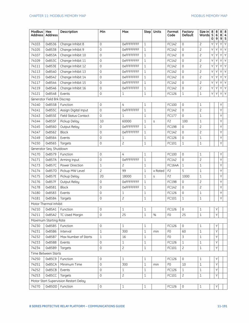
CHAPTER 11: MODBUS MEMORY MAP MODBUS MEMORY MAP
74103 0x8536 Change Inhibit 8 0 0xFFFFFFFF 1 FC142 0 2 Y Y Y Y
74105 0x8538 Change Inhibit 9 0 0xFFFFFFFF 1 FC142 0 2 Y Y Y Y
74107 0x853A Change Inhibit 10 0 0xFFFFFFFF 1 FC142 0 2 Y Y Y Y
74109 0x853C Change Inhibit 11 0 0xFFFFFFFF 1 FC142 0 2 Y Y Y Y
74111 0x853E Change Inhibit 12 0 0xFFFFFFFF 1 FC142 0 2 Y Y Y Y
74113 0x8540 Change Inhibit 13 0 0xFFFFFFFF 1 FC142 0 2 Y Y Y Y
74115 0x8542 Change Inhibit 14 0 0xFFFFFFFF 1 FC142 0 2 Y Y Y Y
74117 0x8544 Change Inhibit 15 0 0xFFFFFFFF 1 FC142 0 2 Y Y Y Y
74119 0x8546 Change Inhibit 16 0 0xFFFFFFFF 1 FC142 0 2 Y Y Y Y
74121 0x8548 Events 0 1 1 FC126 1 1 Y Y Y Y
Generator Field Brk Discrep
74140 0x855B Function 0 4 1 FC100 0 1 Y
74141 0x855C Assign Digital Input 0 0xFFFFFFFF 1 FC142 0 2 Y
74143 0x855E Field Status Contact 0 1 1 FC177 0 1 Y
74144 0x855F Pickup Delay 10 60000 1 s F2 100 1 Y
74145 0x8560 Output Relay 0 0xFFFFFFFF 1 FC198 0 2 Y
74147 0x8562 Block 0 0xFFFFFFFF 1 FC142 0 2 Y
74149 0x8564 Events 0 1 1 FC126 0 1 Y
74150 0x8565 Targets 0 2 1 FC101 1 1 Y
Generator Seq. Shutdown
74170 0x8579 Function 0 4 1 FC100 0 1 Y
74171 0x857A Arming Input 0 0xFFFFFFFF 1 FC142 0 2 Y
74173 0x857C Power Direction 1 2 1 FC164A 1 1 Y
74174 0x857D Pickup MW Level 2 99 1 x Rated F2 5 1 Y
74175 0x857E Pickup Delay 20 18000 1 s F2 1000 1 Y
74176 0x857F Output Relay 0 0xFFFFFFFF 1 FC198 0 2 Y
74178 0x8581 Block 0 0xFFFFFFFF 1 FC142 0 2 Y
74180 0x8583 Events 0 1 1 FC126 0 1 Y
74181 0x8584 Targets 0 2 1 FC101 1 1 Y
Motor Thermal Inhibit
74210 0x85A1 Function 0 1 1 FC126 0 1 Y
74211 0x85A2 TC Used Margin 0 25 1 % F0 25 1 Y
Maximum Starting Rate
74230 0x85B5 Function 0 1 1 FC126 0 1 Y
74231 0x85B6 Interval 1 300 1 min F0 60 1 Y
74232 0x85B7 Max Number of Starts 1 16 1 F0 3 1 Y
74233 0x85B8 Events 0 1 1 FC126 1 1 Y
74234 0x85B9 Targets 0 2 1 FC101 2 1 Y
Time Between Starts
74250 0x85C9 Function 0 1 1 FC126 0 1 Y
74251 0x85CA Minimum Time 0 300 1 min F0 10 1 Y
74252 0x85CB Events 0 1 1 FC126 1 1 Y
74253 0x85CC Targets 0 2 1 FC101 2 1 Y
Motor Start Supervision Restart Delay
74270 0x85DD Function 0 1 1 FC126 0 1 Y
Modbus Address
Hex Address
Description Min Max Step Units Format Code
Factory Default
Size in Words
850
869
889
845
8 SERIES PROTECTIVE RELAY PLATFORM – COMMUNICATIONS GUIDE 11-191
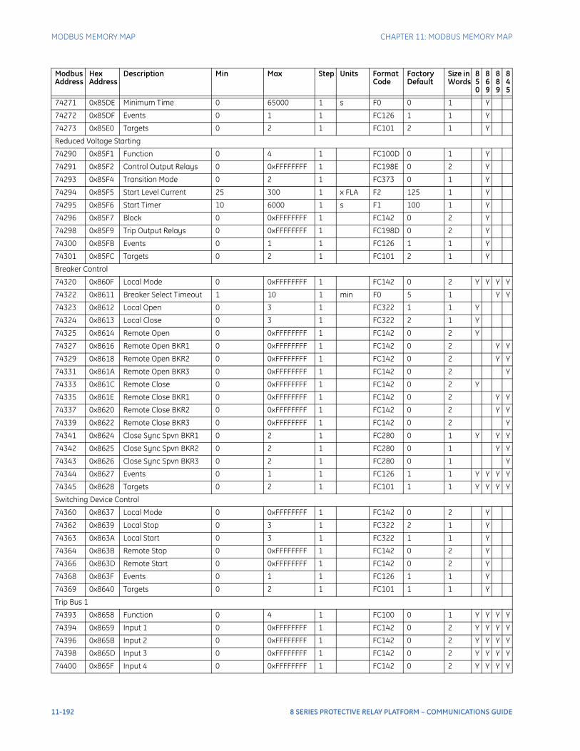
MODBUS MEMORY MAP CHAPTER 11: MODBUS MEMORY MAP
74271 0x85DE Minimum Time 0 65000 1 s F0 0 1 Y
74272 0x85DF Events 0 1 1 FC126 1 1 Y
74273 0x85E0 Targets 0 2 1 FC101 2 1 Y
Reduced Voltage Starting
74290 0x85F1 Function 0 4 1 FC100D 0 1 Y
74291 0x85F2 Control Output Relays 0 0xFFFFFFFF 1 FC198E 0 2 Y
74293 0x85F4 Transition Mode 0 2 1 FC373 0 1 Y
74294 0x85F5 Start Level Current 25 300 1 x FLA F2 125 1 Y
74295 0x85F6 Start Timer 10 6000 1 s F1 100 1 Y
74296 0x85F7 Block 0 0xFFFFFFFF 1 FC142 0 2 Y
74298 0x85F9 Trip Output Relays 0 0xFFFFFFFF 1 FC198D 0 2 Y
74300 0x85FB Events 0 1 1 FC126 1 1 Y
74301 0x85FC Targets 0 2 1 FC101 2 1 Y
Breaker Control
74320 0x860F Local Mode 0 0xFFFFFFFF 1 FC142 0 2 Y Y Y Y
74322 0x8611 Breaker Select Timeout 1 10 1 min F0 5 1 Y Y
74323 0x8612 Local Open 0 3 1 FC322 1 1 Y
74324 0x8613 Local Close 0 3 1 FC322 2 1 Y
74325 0x8614 Remote Open 0 0xFFFFFFFF 1 FC142 0 2 Y
74327 0x8616 Remote Open BKR1 0 0xFFFFFFFF 1 FC142 0 2 Y Y
74329 0x8618 Remote Open BKR2 0 0xFFFFFFFF 1 FC142 0 2 Y Y
74331 0x861A Remote Open BKR3 0 0xFFFFFFFF 1 FC142 0 2 Y
74333 0x861C Remote Close 0 0xFFFFFFFF 1 FC142 0 2 Y
74335 0x861E Remote Close BKR1 0 0xFFFFFFFF 1 FC142 0 2 Y Y
74337 0x8620 Remote Close BKR2 0 0xFFFFFFFF 1 FC142 0 2 Y Y
74339 0x8622 Remote Close BKR3 0 0xFFFFFFFF 1 FC142 0 2 Y
74341 0x8624 Close Sync Spvn BKR1 0 2 1 FC280 0 1 Y Y Y
74342 0x8625 Close Sync Spvn BKR2 0 2 1 FC280 0 1 Y Y
74343 0x8626 Close Sync Spvn BKR3 0 2 1 FC280 0 1 Y
74344 0x8627 Events 0 1 1 FC126 1 1 Y Y Y Y
74345 0x8628 Targets 0 2 1 FC101 1 1 Y Y Y Y
Switching Device Control
74360 0x8637 Local Mode 0 0xFFFFFFFF 1 FC142 0 2 Y
74362 0x8639 Local Stop 0 3 1 FC322 2 1 Y
74363 0x863A Local Start 0 3 1 FC322 1 1 Y
74364 0x863B Remote Stop 0 0xFFFFFFFF 1 FC142 0 2 Y
74366 0x863D Remote Start 0 0xFFFFFFFF 1 FC142 0 2 Y
74368 0x863F Events 0 1 1 FC126 1 1 Y
74369 0x8640 Targets 0 2 1 FC101 1 1 Y
Trip Bus 1
74393 0x8658 Function 0 4 1 FC100 0 1 Y Y Y Y
74394 0x8659 Input 1 0 0xFFFFFFFF 1 FC142 0 2 Y Y Y Y
74396 0x865B Input 2 0 0xFFFFFFFF 1 FC142 0 2 Y Y Y Y
74398 0x865D Input 3 0 0xFFFFFFFF 1 FC142 0 2 Y Y Y Y
74400 0x865F Input 4 0 0xFFFFFFFF 1 FC142 0 2 Y Y Y Y
Modbus Address
Hex Address
Description Min Max Step Units Format Code
Factory Default
Size in Words
850
869
889
845
11-192 8 SERIES PROTECTIVE RELAY PLATFORM – COMMUNICATIONS GUIDE
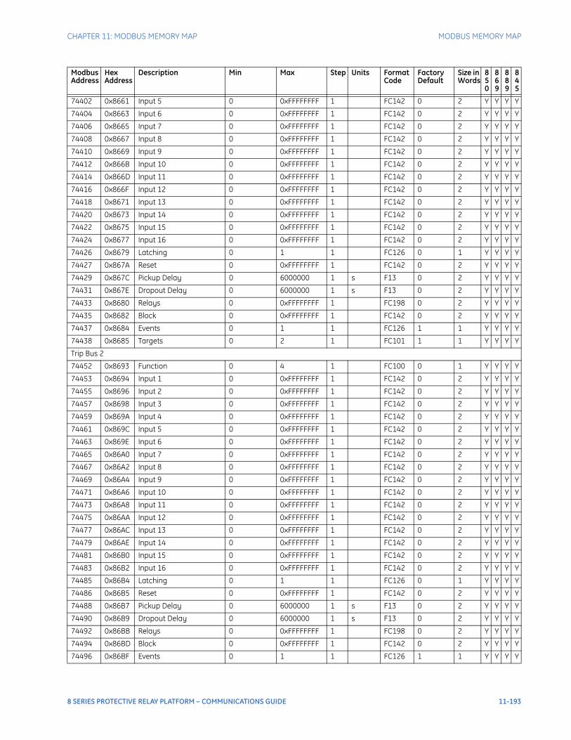
CHAPTER 11: MODBUS MEMORY MAP MODBUS MEMORY MAP
74402 0x8661 Input 5 0 0xFFFFFFFF 1 FC142 0 2 Y Y Y Y
74404 0x8663 Input 6 0 0xFFFFFFFF 1 FC142 0 2 Y Y Y Y
74406 0x8665 Input 7 0 0xFFFFFFFF 1 FC142 0 2 Y Y Y Y
74408 0x8667 Input 8 0 0xFFFFFFFF 1 FC142 0 2 Y Y Y Y
74410 0x8669 Input 9 0 0xFFFFFFFF 1 FC142 0 2 Y Y Y Y
74412 0x866B Input 10 0 0xFFFFFFFF 1 FC142 0 2 Y Y Y Y
74414 0x866D Input 11 0 0xFFFFFFFF 1 FC142 0 2 Y Y Y Y
74416 0x866F Input 12 0 0xFFFFFFFF 1 FC142 0 2 Y Y Y Y
74418 0x8671 Input 13 0 0xFFFFFFFF 1 FC142 0 2 Y Y Y Y
74420 0x8673 Input 14 0 0xFFFFFFFF 1 FC142 0 2 Y Y Y Y
74422 0x8675 Input 15 0 0xFFFFFFFF 1 FC142 0 2 Y Y Y Y
74424 0x8677 Input 16 0 0xFFFFFFFF 1 FC142 0 2 Y Y Y Y
74426 0x8679 Latching 0 1 1 FC126 0 1 Y Y Y Y
74427 0x867A Reset 0 0xFFFFFFFF 1 FC142 0 2 Y Y Y Y
74429 0x867C Pickup Delay 0 6000000 1 s F13 0 2 Y Y Y Y
74431 0x867E Dropout Delay 0 6000000 1 s F13 0 2 Y Y Y Y
74433 0x8680 Relays 0 0xFFFFFFFF 1 FC198 0 2 Y Y Y Y
74435 0x8682 Block 0 0xFFFFFFFF 1 FC142 0 2 Y Y Y Y
74437 0x8684 Events 0 1 1 FC126 1 1 Y Y Y Y
74438 0x8685 Targets 0 2 1 FC101 1 1 Y Y Y Y
Trip Bus 2
74452 0x8693 Function 0 4 1 FC100 0 1 Y Y Y Y
74453 0x8694 Input 1 0 0xFFFFFFFF 1 FC142 0 2 Y Y Y Y
74455 0x8696 Input 2 0 0xFFFFFFFF 1 FC142 0 2 Y Y Y Y
74457 0x8698 Input 3 0 0xFFFFFFFF 1 FC142 0 2 Y Y Y Y
74459 0x869A Input 4 0 0xFFFFFFFF 1 FC142 0 2 Y Y Y Y
74461 0x869C Input 5 0 0xFFFFFFFF 1 FC142 0 2 Y Y Y Y
74463 0x869E Input 6 0 0xFFFFFFFF 1 FC142 0 2 Y Y Y Y
74465 0x86A0 Input 7 0 0xFFFFFFFF 1 FC142 0 2 Y Y Y Y
74467 0x86A2 Input 8 0 0xFFFFFFFF 1 FC142 0 2 Y Y Y Y
74469 0x86A4 Input 9 0 0xFFFFFFFF 1 FC142 0 2 Y Y Y Y
74471 0x86A6 Input 10 0 0xFFFFFFFF 1 FC142 0 2 Y Y Y Y
74473 0x86A8 Input 11 0 0xFFFFFFFF 1 FC142 0 2 Y Y Y Y
74475 0x86AA Input 12 0 0xFFFFFFFF 1 FC142 0 2 Y Y Y Y
74477 0x86AC Input 13 0 0xFFFFFFFF 1 FC142 0 2 Y Y Y Y
74479 0x86AE Input 14 0 0xFFFFFFFF 1 FC142 0 2 Y Y Y Y
74481 0x86B0 Input 15 0 0xFFFFFFFF 1 FC142 0 2 Y Y Y Y
74483 0x86B2 Input 16 0 0xFFFFFFFF 1 FC142 0 2 Y Y Y Y
74485 0x86B4 Latching 0 1 1 FC126 0 1 Y Y Y Y
74486 0x86B5 Reset 0 0xFFFFFFFF 1 FC142 0 2 Y Y Y Y
74488 0x86B7 Pickup Delay 0 6000000 1 s F13 0 2 Y Y Y Y
74490 0x86B9 Dropout Delay 0 6000000 1 s F13 0 2 Y Y Y Y
74492 0x86BB Relays 0 0xFFFFFFFF 1 FC198 0 2 Y Y Y Y
74494 0x86BD Block 0 0xFFFFFFFF 1 FC142 0 2 Y Y Y Y
74496 0x86BF Events 0 1 1 FC126 1 1 Y Y Y Y
Modbus Address
Hex Address
Description Min Max Step Units Format Code
Factory Default
Size in Words
850
869
889
845
8 SERIES PROTECTIVE RELAY PLATFORM – COMMUNICATIONS GUIDE 11-193
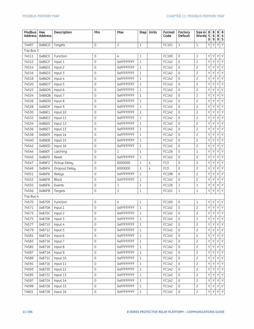
MODBUS MEMORY MAP CHAPTER 11: MODBUS MEMORY MAP
74497 0x86C0 Targets 0 2 1 FC101 1 1 Y Y Y Y
Trip Bus 3
74511 0x86CE Function 0 4 1 FC100 0 1 Y Y Y Y
74512 0x86CF Input 1 0 0xFFFFFFFF 1 FC142 0 2 Y Y Y Y
74514 0x86D1 Input 2 0 0xFFFFFFFF 1 FC142 0 2 Y Y Y Y
74516 0x86D3 Input 3 0 0xFFFFFFFF 1 FC142 0 2 Y Y Y Y
74518 0x86D5 Input 4 0 0xFFFFFFFF 1 FC142 0 2 Y Y Y Y
74520 0x86D7 Input 5 0 0xFFFFFFFF 1 FC142 0 2 Y Y Y Y
74522 0x86D9 Input 6 0 0xFFFFFFFF 1 FC142 0 2 Y Y Y Y
74524 0x86DB Input 7 0 0xFFFFFFFF 1 FC142 0 2 Y Y Y Y
74526 0x86DD Input 8 0 0xFFFFFFFF 1 FC142 0 2 Y Y Y Y
74528 0x86DF Input 9 0 0xFFFFFFFF 1 FC142 0 2 Y Y Y Y
74530 0x86E1 Input 10 0 0xFFFFFFFF 1 FC142 0 2 Y Y Y Y
74532 0x86E3 Input 11 0 0xFFFFFFFF 1 FC142 0 2 Y Y Y Y
74534 0x86E5 Input 12 0 0xFFFFFFFF 1 FC142 0 2 Y Y Y Y
74536 0x86E7 Input 13 0 0xFFFFFFFF 1 FC142 0 2 Y Y Y Y
74538 0x86E9 Input 14 0 0xFFFFFFFF 1 FC142 0 2 Y Y Y Y
74540 0x86EB Input 15 0 0xFFFFFFFF 1 FC142 0 2 Y Y Y Y
74542 0x86ED Input 16 0 0xFFFFFFFF 1 FC142 0 2 Y Y Y Y
74544 0x86EF Latching 0 1 1 FC126 0 1 Y Y Y Y
74545 0x86F0 Reset 0 0xFFFFFFFF 1 FC142 0 2 Y Y Y Y
74547 0x86F2 Pickup Delay 0 6000000 1 s F13 0 2 Y Y Y Y
74549 0x86F4 Dropout Delay 0 6000000 1 s F13 0 2 Y Y Y Y
74551 0x86F6 Relays 0 0xFFFFFFFF 1 FC198 0 2 Y Y Y Y
74553 0x86F8 Block 0 0xFFFFFFFF 1 FC142 0 2 Y Y Y Y
74555 0x86FA Events 0 1 1 FC126 1 1 Y Y Y Y
74556 0x86FB Targets 0 2 1 FC101 1 1 Y Y Y Y
Trip Bus 4
74570 0x8709 Function 0 4 1 FC100 0 1 Y Y Y Y
74571 0x870A Input 1 0 0xFFFFFFFF 1 FC142 0 2 Y Y Y Y
74573 0x870C Input 2 0 0xFFFFFFFF 1 FC142 0 2 Y Y Y Y
74575 0x870E Input 3 0 0xFFFFFFFF 1 FC142 0 2 Y Y Y Y
74577 0x8710 Input 4 0 0xFFFFFFFF 1 FC142 0 2 Y Y Y Y
74579 0x8712 Input 5 0 0xFFFFFFFF 1 FC142 0 2 Y Y Y Y
74581 0x8714 Input 6 0 0xFFFFFFFF 1 FC142 0 2 Y Y Y Y
74583 0x8716 Input 7 0 0xFFFFFFFF 1 FC142 0 2 Y Y Y Y
74585 0x8718 Input 8 0 0xFFFFFFFF 1 FC142 0 2 Y Y Y Y
74587 0x871A Input 9 0 0xFFFFFFFF 1 FC142 0 2 Y Y Y Y
74589 0x871C Input 10 0 0xFFFFFFFF 1 FC142 0 2 Y Y Y Y
74591 0x871E Input 11 0 0xFFFFFFFF 1 FC142 0 2 Y Y Y Y
74593 0x8720 Input 12 0 0xFFFFFFFF 1 FC142 0 2 Y Y Y Y
74595 0x8722 Input 13 0 0xFFFFFFFF 1 FC142 0 2 Y Y Y Y
74597 0x8724 Input 14 0 0xFFFFFFFF 1 FC142 0 2 Y Y Y Y
74599 0x8726 Input 15 0 0xFFFFFFFF 1 FC142 0 2 Y Y Y Y
74601 0x8728 Input 16 0 0xFFFFFFFF 1 FC142 0 2 Y Y Y Y
Modbus Address
Hex Address
Description Min Max Step Units Format Code
Factory Default
Size in Words
850
869
889
845
11-194 8 SERIES PROTECTIVE RELAY PLATFORM – COMMUNICATIONS GUIDE

CHAPTER 11: MODBUS MEMORY MAP MODBUS MEMORY MAP
74603 0x872A Latching 0 1 1 FC126 0 1 Y Y Y Y
74604 0x872B Reset 0 0xFFFFFFFF 1 FC142 0 2 Y Y Y Y
74606 0x872D Pickup Delay 0 6000000 1 s F13 0 2 Y Y Y Y
74608 0x872F Dropout Delay 0 6000000 1 s F13 0 2 Y Y Y Y
74610 0x8731 Relays 0 0xFFFFFFFF 1 FC198 0 2 Y Y Y Y
74612 0x8733 Block 0 0xFFFFFFFF 1 FC142 0 2 Y Y Y Y
74614 0x8735 Events 0 1 1 FC126 1 1 Y Y Y Y
74615 0x8736 Targets 0 2 1 FC101 1 1 Y Y Y Y
Trip Bus 5
74629 0x8744 Function 0 4 1 FC100 0 1 Y Y Y Y
74630 0x8745 Input 1 0 0xFFFFFFFF 1 FC142 0 2 Y Y Y Y
74632 0x8747 Input 2 0 0xFFFFFFFF 1 FC142 0 2 Y Y Y Y
74634 0x8749 Input 3 0 0xFFFFFFFF 1 FC142 0 2 Y Y Y Y
74636 0x874B Input 4 0 0xFFFFFFFF 1 FC142 0 2 Y Y Y Y
74638 0x874D Input 5 0 0xFFFFFFFF 1 FC142 0 2 Y Y Y Y
74640 0x874F Input 6 0 0xFFFFFFFF 1 FC142 0 2 Y Y Y Y
74642 0x8751 Input 7 0 0xFFFFFFFF 1 FC142 0 2 Y Y Y Y
74644 0x8753 Input 8 0 0xFFFFFFFF 1 FC142 0 2 Y Y Y Y
74646 0x8755 Input 9 0 0xFFFFFFFF 1 FC142 0 2 Y Y Y Y
74648 0x8757 Input 10 0 0xFFFFFFFF 1 FC142 0 2 Y Y Y Y
74650 0x8759 Input 11 0 0xFFFFFFFF 1 FC142 0 2 Y Y Y Y
74652 0x875B Input 12 0 0xFFFFFFFF 1 FC142 0 2 Y Y Y Y
74654 0x875D Input 13 0 0xFFFFFFFF 1 FC142 0 2 Y Y Y Y
74656 0x875F Input 14 0 0xFFFFFFFF 1 FC142 0 2 Y Y Y Y
74658 0x8761 Input 15 0 0xFFFFFFFF 1 FC142 0 2 Y Y Y Y
74660 0x8763 Input 16 0 0xFFFFFFFF 1 FC142 0 2 Y Y Y Y
74662 0x8765 Latching 0 1 1 FC126 0 1 Y Y Y Y
74663 0x8766 Reset 0 0xFFFFFFFF 1 FC142 0 2 Y Y Y Y
74665 0x8768 Pickup Delay 0 6000000 1 s F13 0 2 Y Y Y Y
74667 0x876A Dropout Delay 0 6000000 1 s F13 0 2 Y Y Y Y
74669 0x876C Relays 0 0xFFFFFFFF 1 FC198 0 2 Y Y Y Y
74671 0x876E Block 0 0xFFFFFFFF 1 FC142 0 2 Y Y Y Y
74673 0x8770 Events 0 1 1 FC126 1 1 Y Y Y Y
74674 0x8771 Targets 0 2 1 FC101 1 1 Y Y Y Y
Trip Bus 6
74688 0x877F Function 0 4 1 FC100 0 1 Y Y Y Y
74689 0x8780 Input 1 0 0xFFFFFFFF 1 FC142 0 2 Y Y Y Y
74691 0x8782 Input 2 0 0xFFFFFFFF 1 FC142 0 2 Y Y Y Y
74693 0x8784 Input 3 0 0xFFFFFFFF 1 FC142 0 2 Y Y Y Y
74695 0x8786 Input 4 0 0xFFFFFFFF 1 FC142 0 2 Y Y Y Y
74697 0x8788 Input 5 0 0xFFFFFFFF 1 FC142 0 2 Y Y Y Y
74699 0x878A Input 6 0 0xFFFFFFFF 1 FC142 0 2 Y Y Y Y
74701 0x878C Input 7 0 0xFFFFFFFF 1 FC142 0 2 Y Y Y Y
74703 0x878E Input 8 0 0xFFFFFFFF 1 FC142 0 2 Y Y Y Y
74705 0x8790 Input 9 0 0xFFFFFFFF 1 FC142 0 2 Y Y Y Y
Modbus Address
Hex Address
Description Min Max Step Units Format Code
Factory Default
Size in Words
850
869
889
845
8 SERIES PROTECTIVE RELAY PLATFORM – COMMUNICATIONS GUIDE 11-195
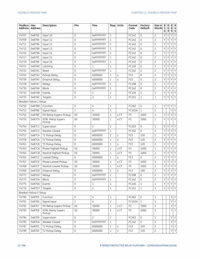
MODBUS MEMORY MAP CHAPTER 11: MODBUS MEMORY MAP
74707 0x8792 Input 10 0 0xFFFFFFFF 1 FC142 0 2 Y Y Y Y
74709 0x8794 Input 11 0 0xFFFFFFFF 1 FC142 0 2 Y Y Y Y
74711 0x8796 Input 12 0 0xFFFFFFFF 1 FC142 0 2 Y Y Y Y
74713 0x8798 Input 13 0 0xFFFFFFFF 1 FC142 0 2 Y Y Y Y
74715 0x879A Input 14 0 0xFFFFFFFF 1 FC142 0 2 Y Y Y Y
74717 0x879C Input 15 0 0xFFFFFFFF 1 FC142 0 2 Y Y Y Y
74719 0x879E Input 16 0 0xFFFFFFFF 1 FC142 0 2 Y Y Y Y
74721 0x87A0 Latching 0 1 1 FC126 0 1 Y Y Y Y
74722 0x87A1 Reset 0 0xFFFFFFFF 1 FC142 0 2 Y Y Y Y
74724 0x87A3 Pickup Delay 0 6000000 1 s F13 0 2 Y Y Y Y
74726 0x87A5 Dropout Delay 0 6000000 1 s F13 0 2 Y Y Y Y
74728 0x87A7 Relays 0 0xFFFFFFFF 1 FC198 0 2 Y Y Y Y
74730 0x87A9 Block 0 0xFFFFFFFF 1 FC142 0 2 Y Y Y Y
74732 0x87AB Events 0 1 1 FC126 1 1 Y Y Y Y
74733 0x87AC Targets 0 2 1 FC101 1 1 Y Y Y Y
Breaker Failure 1 Setup
74750 0x87BD Function 0 4 1 FC262 0 1 Y Y Y Y
74751 0x87BE Signal Input 1 4 1 FC102A 1 1 Y Y
74752 0x87BF PH Retrip Superv Pickup 50 30000 1 x CT F3 1000 1 Y Y Y Y
74753 0x87C0 NTRL Retrip Superv Pickup
50 30000 1 x CT F3 1000 1 Y Y Y Y
74754 0x87C1 Supervision 0 2 1 FC263 0 1 Y Y Y Y
74755 0x87C2 Breaker Closed 0 0xFFFFFFFF 1 FC142 0 2 Y Y Y Y
74757 0x87C4 T1 Pickup Delay 0 6000000 1 s F13 120 2 Y Y Y Y
74759 0x87C6 T2 Pickup Delay 0 6000000 1 s F13 120 2 Y Y Y Y
74761 0x87C8 T3 Pickup Delay 0 6000000 1 s F13 120 2 Y Y Y Y
74763 0x87CA Phase Highset Pickup 50 30000 1 x CT F3 1000 1 Y Y Y Y
74764 0x87CB Neutral Highset Pickup 50 30000 1 x CT F3 1000 1 Y Y Y Y
74765 0x87CC Lowset Delay 0 6000000 1 s F13 0 2 Y Y Y Y
74767 0x87CE Phase Lowset Pickup 50 30000 1 x CT F3 1000 1 Y Y Y Y
74768 0x87CF Neutral Lowset Pickup 50 30000 1 x CT F3 1000 1 Y Y Y Y
74769 0x87D0 Dropout Delay 0 6000000 1 s F13 100 2 Y Y Y Y
74771 0x87D2 Relays 0 0xFFFFFFFF 1 FC198 0 2 Y Y Y Y
74773 0x87D4 Block 0 0xFFFFFFFF 1 FC142 0 2 Y Y Y Y
74775 0x87D6 Events 0 1 1 FC126 1 1 Y Y Y Y
74776 0x87D7 Targets 0 2 1 FC101 1 1 Y Y Y Y
Breaker Failure 2 Setup
74790 0x87E5 Function 0 4 1 FC262 0 1 Y Y
74791 0x87E6 Signal Input 1 4 1 FC102A 1 1 Y Y
74792 0x87E7 PH Retrip Superv Pickup 50 30000 1 x CT F3 1000 1 Y Y
74793 0x87E8 NTRL Retrip Superv Pickup
50 30000 1 x CT F3 1000 1 Y Y
74794 0x87E9 Supervision 0 2 1 FC263 0 1 Y Y
74795 0x87EA Breaker Closed 0 0xFFFFFFFF 1 FC142 0 2 Y Y
74797 0x87EC T1 Pickup Delay 0 6000000 1 s F13 120 2 Y Y
74799 0x87EE T2 Pickup Delay 0 6000000 1 s F13 120 2 Y Y
Modbus Address
Hex Address
Description Min Max Step Units Format Code
Factory Default
Size in Words
850
869
889
845
11-196 8 SERIES PROTECTIVE RELAY PLATFORM – COMMUNICATIONS GUIDE
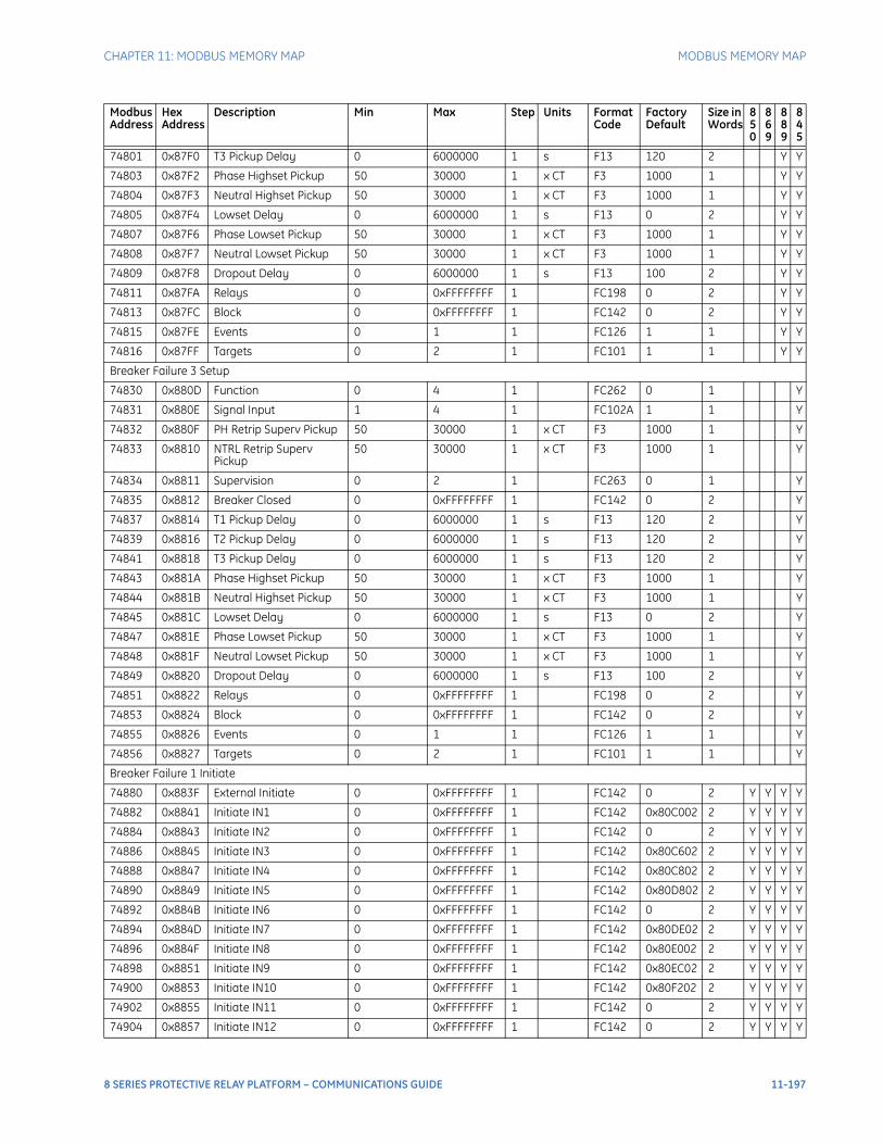
CHAPTER 11: MODBUS MEMORY MAP MODBUS MEMORY MAP
74801 0x87F0 T3 Pickup Delay 0 6000000 1 s F13 120 2 Y Y
74803 0x87F2 Phase Highset Pickup 50 30000 1 x CT F3 1000 1 Y Y
74804 0x87F3 Neutral Highset Pickup 50 30000 1 x CT F3 1000 1 Y Y
74805 0x87F4 Lowset Delay 0 6000000 1 s F13 0 2 Y Y
74807 0x87F6 Phase Lowset Pickup 50 30000 1 x CT F3 1000 1 Y Y
74808 0x87F7 Neutral Lowset Pickup 50 30000 1 x CT F3 1000 1 Y Y
74809 0x87F8 Dropout Delay 0 6000000 1 s F13 100 2 Y Y
74811 0x87FA Relays 0 0xFFFFFFFF 1 FC198 0 2 Y Y
74813 0x87FC Block 0 0xFFFFFFFF 1 FC142 0 2 Y Y
74815 0x87FE Events 0 1 1 FC126 1 1 Y Y
74816 0x87FF Targets 0 2 1 FC101 1 1 Y Y
Breaker Failure 3 Setup
74830 0x880D Function 0 4 1 FC262 0 1 Y
74831 0x880E Signal Input 1 4 1 FC102A 1 1 Y
74832 0x880F PH Retrip Superv Pickup 50 30000 1 x CT F3 1000 1 Y
74833 0x8810 NTRL Retrip Superv Pickup
50 30000 1 x CT F3 1000 1 Y
74834 0x8811 Supervision 0 2 1 FC263 0 1 Y
74835 0x8812 Breaker Closed 0 0xFFFFFFFF 1 FC142 0 2 Y
74837 0x8814 T1 Pickup Delay 0 6000000 1 s F13 120 2 Y
74839 0x8816 T2 Pickup Delay 0 6000000 1 s F13 120 2 Y
74841 0x8818 T3 Pickup Delay 0 6000000 1 s F13 120 2 Y
74843 0x881A Phase Highset Pickup 50 30000 1 x CT F3 1000 1 Y
74844 0x881B Neutral Highset Pickup 50 30000 1 x CT F3 1000 1 Y
74845 0x881C Lowset Delay 0 6000000 1 s F13 0 2 Y
74847 0x881E Phase Lowset Pickup 50 30000 1 x CT F3 1000 1 Y
74848 0x881F Neutral Lowset Pickup 50 30000 1 x CT F3 1000 1 Y
74849 0x8820 Dropout Delay 0 6000000 1 s F13 100 2 Y
74851 0x8822 Relays 0 0xFFFFFFFF 1 FC198 0 2 Y
74853 0x8824 Block 0 0xFFFFFFFF 1 FC142 0 2 Y
74855 0x8826 Events 0 1 1 FC126 1 1 Y
74856 0x8827 Targets 0 2 1 FC101 1 1 Y
Breaker Failure 1 Initiate
74880 0x883F External Initiate 0 0xFFFFFFFF 1 FC142 0 2 Y Y Y Y
74882 0x8841 Initiate IN1 0 0xFFFFFFFF 1 FC142 0x80C002 2 Y Y Y Y
74884 0x8843 Initiate IN2 0 0xFFFFFFFF 1 FC142 0 2 Y Y Y Y
74886 0x8845 Initiate IN3 0 0xFFFFFFFF 1 FC142 0x80C602 2 Y Y Y Y
74888 0x8847 Initiate IN4 0 0xFFFFFFFF 1 FC142 0x80C802 2 Y Y Y Y
74890 0x8849 Initiate IN5 0 0xFFFFFFFF 1 FC142 0x80D802 2 Y Y Y Y
74892 0x884B Initiate IN6 0 0xFFFFFFFF 1 FC142 0 2 Y Y Y Y
74894 0x884D Initiate IN7 0 0xFFFFFFFF 1 FC142 0x80DE02 2 Y Y Y Y
74896 0x884F Initiate IN8 0 0xFFFFFFFF 1 FC142 0x80E002 2 Y Y Y Y
74898 0x8851 Initiate IN9 0 0xFFFFFFFF 1 FC142 0x80EC02 2 Y Y Y Y
74900 0x8853 Initiate IN10 0 0xFFFFFFFF 1 FC142 0x80F202 2 Y Y Y Y
74902 0x8855 Initiate IN11 0 0xFFFFFFFF 1 FC142 0 2 Y Y Y Y
74904 0x8857 Initiate IN12 0 0xFFFFFFFF 1 FC142 0 2 Y Y Y Y
Modbus Address
Hex Address
Description Min Max Step Units Format Code
Factory Default
Size in Words
850
869
889
845
8 SERIES PROTECTIVE RELAY PLATFORM – COMMUNICATIONS GUIDE 11-197
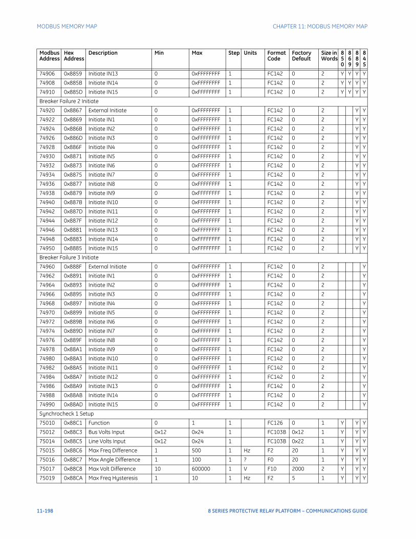
MODBUS MEMORY MAP CHAPTER 11: MODBUS MEMORY MAP
74906 0x8859 Initiate IN13 0 0xFFFFFFFF 1 FC142 0 2 Y Y Y Y
74908 0x885B Initiate IN14 0 0xFFFFFFFF 1 FC142 0 2 Y Y Y Y
74910 0x885D Initiate IN15 0 0xFFFFFFFF 1 FC142 0 2 Y Y Y Y
Breaker Failure 2 Initiate
74920 0x8867 External Initiate 0 0xFFFFFFFF 1 FC142 0 2 Y Y
74922 0x8869 Initiate IN1 0 0xFFFFFFFF 1 FC142 0 2 Y Y
74924 0x886B Initiate IN2 0 0xFFFFFFFF 1 FC142 0 2 Y Y
74926 0x886D Initiate IN3 0 0xFFFFFFFF 1 FC142 0 2 Y Y
74928 0x886F Initiate IN4 0 0xFFFFFFFF 1 FC142 0 2 Y Y
74930 0x8871 Initiate IN5 0 0xFFFFFFFF 1 FC142 0 2 Y Y
74932 0x8873 Initiate IN6 0 0xFFFFFFFF 1 FC142 0 2 Y Y
74934 0x8875 Initiate IN7 0 0xFFFFFFFF 1 FC142 0 2 Y Y
74936 0x8877 Initiate IN8 0 0xFFFFFFFF 1 FC142 0 2 Y Y
74938 0x8879 Initiate IN9 0 0xFFFFFFFF 1 FC142 0 2 Y Y
74940 0x887B Initiate IN10 0 0xFFFFFFFF 1 FC142 0 2 Y Y
74942 0x887D Initiate IN11 0 0xFFFFFFFF 1 FC142 0 2 Y Y
74944 0x887F Initiate IN12 0 0xFFFFFFFF 1 FC142 0 2 Y Y
74946 0x8881 Initiate IN13 0 0xFFFFFFFF 1 FC142 0 2 Y Y
74948 0x8883 Initiate IN14 0 0xFFFFFFFF 1 FC142 0 2 Y Y
74950 0x8885 Initiate IN15 0 0xFFFFFFFF 1 FC142 0 2 Y Y
Breaker Failure 3 Initiate
74960 0x888F External Initiate 0 0xFFFFFFFF 1 FC142 0 2 Y
74962 0x8891 Initiate IN1 0 0xFFFFFFFF 1 FC142 0 2 Y
74964 0x8893 Initiate IN2 0 0xFFFFFFFF 1 FC142 0 2 Y
74966 0x8895 Initiate IN3 0 0xFFFFFFFF 1 FC142 0 2 Y
74968 0x8897 Initiate IN4 0 0xFFFFFFFF 1 FC142 0 2 Y
74970 0x8899 Initiate IN5 0 0xFFFFFFFF 1 FC142 0 2 Y
74972 0x889B Initiate IN6 0 0xFFFFFFFF 1 FC142 0 2 Y
74974 0x889D Initiate IN7 0 0xFFFFFFFF 1 FC142 0 2 Y
74976 0x889F Initiate IN8 0 0xFFFFFFFF 1 FC142 0 2 Y
74978 0x88A1 Initiate IN9 0 0xFFFFFFFF 1 FC142 0 2 Y
74980 0x88A3 Initiate IN10 0 0xFFFFFFFF 1 FC142 0 2 Y
74982 0x88A5 Initiate IN11 0 0xFFFFFFFF 1 FC142 0 2 Y
74984 0x88A7 Initiate IN12 0 0xFFFFFFFF 1 FC142 0 2 Y
74986 0x88A9 Initiate IN13 0 0xFFFFFFFF 1 FC142 0 2 Y
74988 0x88AB Initiate IN14 0 0xFFFFFFFF 1 FC142 0 2 Y
74990 0x88AD Initiate IN15 0 0xFFFFFFFF 1 FC142 0 2 Y
Synchrocheck 1 Setup
75010 0x88C1 Function 0 1 1 FC126 0 1 Y Y Y
75012 0x88C3 Bus Volts Input 0x12 0x24 1 FC103B 0x12 1 Y Y Y
75014 0x88C5 Line Volts Input 0x12 0x24 1 FC103B 0x22 1 Y Y Y
75015 0x88C6 Max Freq Difference 1 500 1 Hz F2 20 1 Y Y Y
75016 0x88C7 Max Angle Difference 1 100 1 ? F0 20 1 Y Y Y
75017 0x88C8 Max Volt Difference 10 600000 1 V F10 2000 2 Y Y Y
75019 0x88CA Max Freq Hysteresis 1 10 1 Hz F2 5 1 Y Y Y
Modbus Address
Hex Address
Description Min Max Step Units Format Code
Factory Default
Size in Words
850
869
889
845
11-198 8 SERIES PROTECTIVE RELAY PLATFORM – COMMUNICATIONS GUIDE
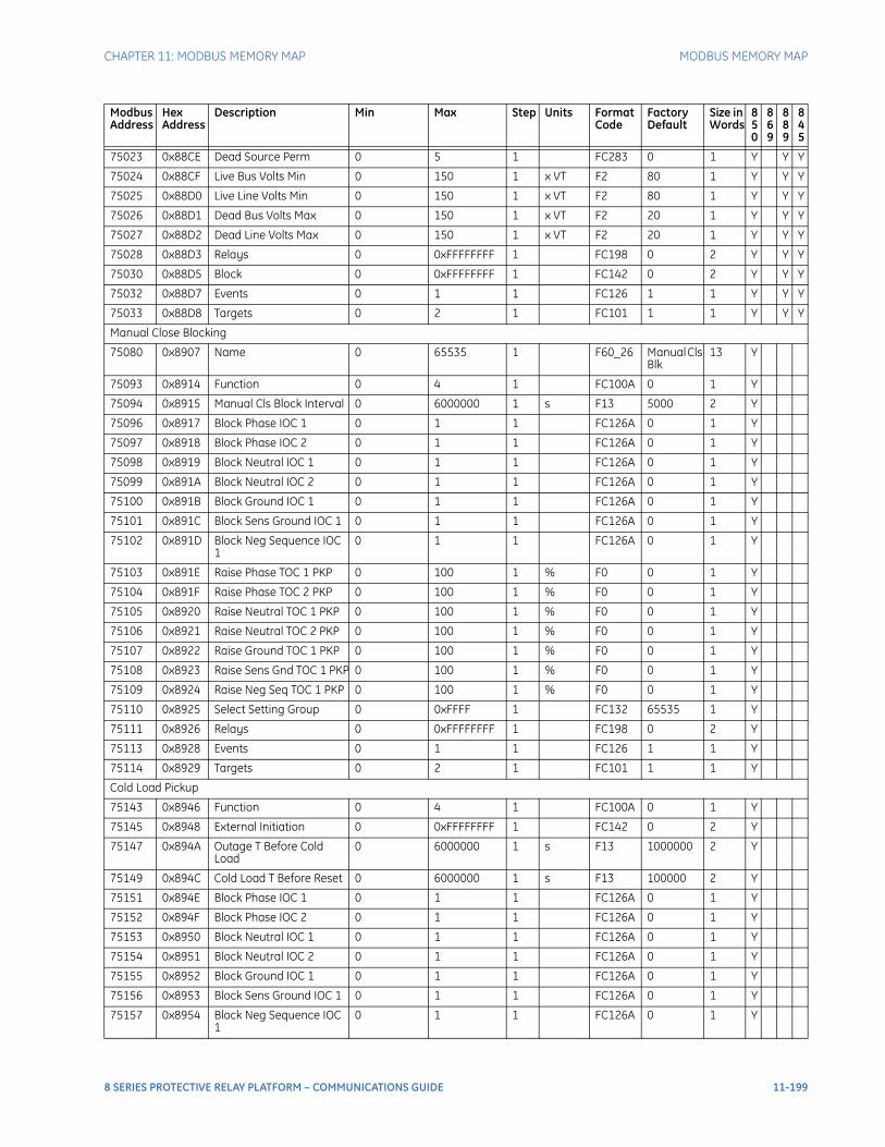
CHAPTER 11: MODBUS MEMORY MAP MODBUS MEMORY MAP
75023 0x88CE Dead Source Perm 0 5 1 FC283 0 1 Y Y Y
75024 0x88CF Live Bus Volts Min 0 150 1 x VT F2 80 1 Y Y Y
75025 0x88D0 Live Line Volts Min 0 150 1 x VT F2 80 1 Y Y Y
75026 0x88D1 Dead Bus Volts Max 0 150 1 x VT F2 20 1 Y Y Y
75027 0x88D2 Dead Line Volts Max 0 150 1 x VT F2 20 1 Y Y Y
75028 0x88D3 Relays 0 0xFFFFFFFF 1 FC198 0 2 Y Y Y
75030 0x88D5 Block 0 0xFFFFFFFF 1 FC142 0 2 Y Y Y
75032 0x88D7 Events 0 1 1 FC126 1 1 Y Y Y
75033 0x88D8 Targets 0 2 1 FC101 1 1 Y Y Y
Manual Close Blocking
75080 0x8907 Name 0 65535 1 F60_26 Manual Cls Blk
13 Y
75093 0x8914 Function 0 4 1 FC100A 0 1 Y
75094 0x8915 Manual Cls Block Interval 0 6000000 1 s F13 5000 2 Y
75096 0x8917 Block Phase IOC 1 0 1 1 FC126A 0 1 Y
75097 0x8918 Block Phase IOC 2 0 1 1 FC126A 0 1 Y
75098 0x8919 Block Neutral IOC 1 0 1 1 FC126A 0 1 Y
75099 0x891A Block Neutral IOC 2 0 1 1 FC126A 0 1 Y
75100 0x891B Block Ground IOC 1 0 1 1 FC126A 0 1 Y
75101 0x891C Block Sens Ground IOC 1 0 1 1 FC126A 0 1 Y
75102 0x891D Block Neg Sequence IOC 1
0 1 1 FC126A 0 1 Y
75103 0x891E Raise Phase TOC 1 PKP 0 100 1 % F0 0 1 Y
75104 0x891F Raise Phase TOC 2 PKP 0 100 1 % F0 0 1 Y
75105 0x8920 Raise Neutral TOC 1 PKP 0 100 1 % F0 0 1 Y
75106 0x8921 Raise Neutral TOC 2 PKP 0 100 1 % F0 0 1 Y
75107 0x8922 Raise Ground TOC 1 PKP 0 100 1 % F0 0 1 Y
75108 0x8923 Raise Sens Gnd TOC 1 PKP 0 100 1 % F0 0 1 Y
75109 0x8924 Raise Neg Seq TOC 1 PKP 0 100 1 % F0 0 1 Y
75110 0x8925 Select Setting Group 0 0xFFFF 1 FC132 65535 1 Y
75111 0x8926 Relays 0 0xFFFFFFFF 1 FC198 0 2 Y
75113 0x8928 Events 0 1 1 FC126 1 1 Y
75114 0x8929 Targets 0 2 1 FC101 1 1 Y
Cold Load Pickup
75143 0x8946 Function 0 4 1 FC100A 0 1 Y
75145 0x8948 External Initiation 0 0xFFFFFFFF 1 FC142 0 2 Y
75147 0x894A Outage T Before Cold Load
0 6000000 1 s F13 1000000 2 Y
75149 0x894C Cold Load T Before Reset 0 6000000 1 s F13 100000 2 Y
75151 0x894E Block Phase IOC 1 0 1 1 FC126A 0 1 Y
75152 0x894F Block Phase IOC 2 0 1 1 FC126A 0 1 Y
75153 0x8950 Block Neutral IOC 1 0 1 1 FC126A 0 1 Y
75154 0x8951 Block Neutral IOC 2 0 1 1 FC126A 0 1 Y
75155 0x8952 Block Ground IOC 1 0 1 1 FC126A 0 1 Y
75156 0x8953 Block Sens Ground IOC 1 0 1 1 FC126A 0 1 Y
75157 0x8954 Block Neg Sequence IOC 1
0 1 1 FC126A 0 1 Y
Modbus Address
Hex Address
Description Min Max Step Units Format Code
Factory Default
Size in Words
850
869
889
845
8 SERIES PROTECTIVE RELAY PLATFORM – COMMUNICATIONS GUIDE 11-199
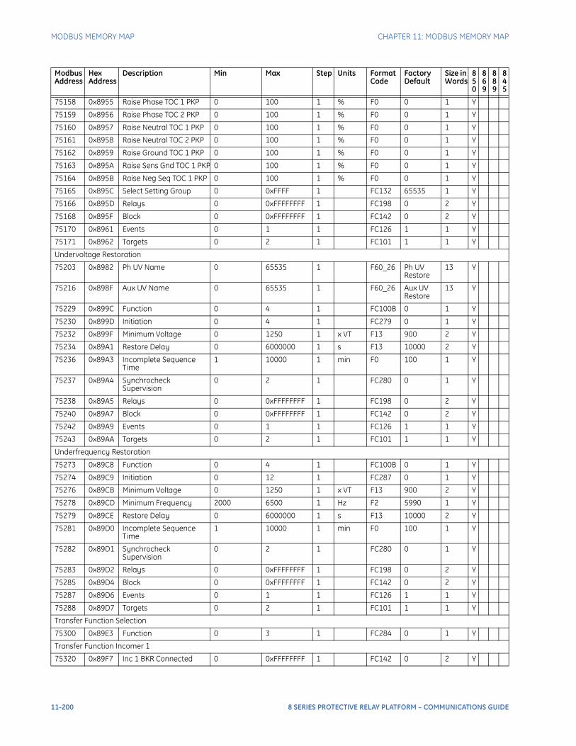
MODBUS MEMORY MAP CHAPTER 11: MODBUS MEMORY MAP
75158 0x8955 Raise Phase TOC 1 PKP 0 100 1 % F0 0 1 Y
75159 0x8956 Raise Phase TOC 2 PKP 0 100 1 % F0 0 1 Y
75160 0x8957 Raise Neutral TOC 1 PKP 0 100 1 % F0 0 1 Y
75161 0x8958 Raise Neutral TOC 2 PKP 0 100 1 % F0 0 1 Y
75162 0x8959 Raise Ground TOC 1 PKP 0 100 1 % F0 0 1 Y
75163 0x895A Raise Sens Gnd TOC 1 PKP 0 100 1 % F0 0 1 Y
75164 0x895B Raise Neg Seq TOC 1 PKP 0 100 1 % F0 0 1 Y
75165 0x895C Select Setting Group 0 0xFFFF 1 FC132 65535 1 Y
75166 0x895D Relays 0 0xFFFFFFFF 1 FC198 0 2 Y
75168 0x895F Block 0 0xFFFFFFFF 1 FC142 0 2 Y
75170 0x8961 Events 0 1 1 FC126 1 1 Y
75171 0x8962 Targets 0 2 1 FC101 1 1 Y
Undervoltage Restoration
75203 0x8982 Ph UV Name 0 65535 1 F60_26 Ph UV Restore
13 Y
75216 0x898F Aux UV Name 0 65535 1 F60_26 Aux UV Restore
13 Y
75229 0x899C Function 0 4 1 FC100B 0 1 Y
75230 0x899D Initiation 0 4 1 FC279 0 1 Y
75232 0x899F Minimum Voltage 0 1250 1 x VT F13 900 2 Y
75234 0x89A1 Restore Delay 0 6000000 1 s F13 10000 2 Y
75236 0x89A3 Incomplete Sequence Time
1 10000 1 min F0 100 1 Y
75237 0x89A4 Synchrocheck Supervision
0 2 1 FC280 0 1 Y
75238 0x89A5 Relays 0 0xFFFFFFFF 1 FC198 0 2 Y
75240 0x89A7 Block 0 0xFFFFFFFF 1 FC142 0 2 Y
75242 0x89A9 Events 0 1 1 FC126 1 1 Y
75243 0x89AA Targets 0 2 1 FC101 1 1 Y
Underfrequency Restoration
75273 0x89C8 Function 0 4 1 FC100B 0 1 Y
75274 0x89C9 Initiation 0 12 1 FC287 0 1 Y
75276 0x89CB Minimum Voltage 0 1250 1 x VT F13 900 2 Y
75278 0x89CD Minimum Frequency 2000 6500 1 Hz F2 5990 1 Y
75279 0x89CE Restore Delay 0 6000000 1 s F13 10000 2 Y
75281 0x89D0 Incomplete Sequence Time
1 10000 1 min F0 100 1 Y
75282 0x89D1 Synchrocheck Supervision
0 2 1 FC280 0 1 Y
75283 0x89D2 Relays 0 0xFFFFFFFF 1 FC198 0 2 Y
75285 0x89D4 Block 0 0xFFFFFFFF 1 FC142 0 2 Y
75287 0x89D6 Events 0 1 1 FC126 1 1 Y
75288 0x89D7 Targets 0 2 1 FC101 1 1 Y
Transfer Function Selection
75300 0x89E3 Function 0 3 1 FC284 0 1 Y
Transfer Function Incomer 1
75320 0x89F7 Inc 1 BKR Connected 0 0xFFFFFFFF 1 FC142 0 2 Y
Modbus Address
Hex Address
Description Min Max Step Units Format Code
Factory Default
Size in Words
850
869
889
845
11-200 8 SERIES PROTECTIVE RELAY PLATFORM – COMMUNICATIONS GUIDE
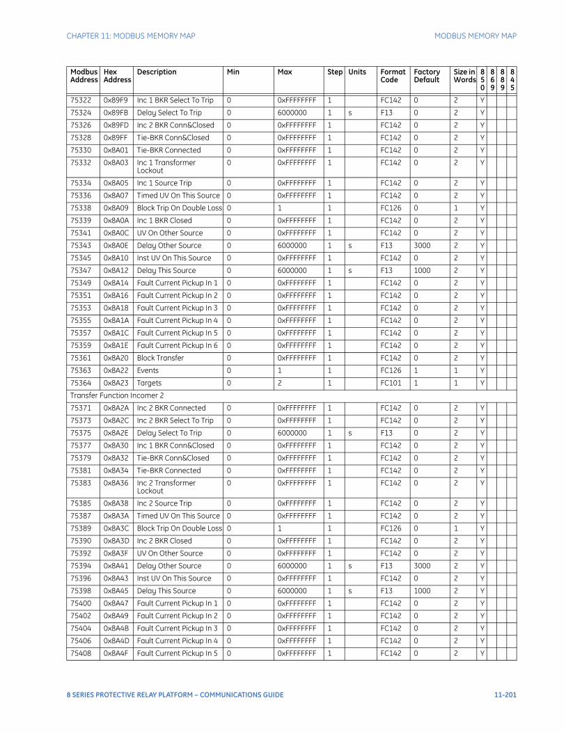
CHAPTER 11: MODBUS MEMORY MAP MODBUS MEMORY MAP
75322 0x89F9 Inc 1 BKR Select To Trip 0 0xFFFFFFFF 1 FC142 0 2 Y
75324 0x89FB Delay Select To Trip 0 6000000 1 s F13 0 2 Y
75326 0x89FD Inc 2 BKR Conn&Closed 0 0xFFFFFFFF 1 FC142 0 2 Y
75328 0x89FF Tie-BKR Conn&Closed 0 0xFFFFFFFF 1 FC142 0 2 Y
75330 0x8A01 Tie-BKR Connected 0 0xFFFFFFFF 1 FC142 0 2 Y
75332 0x8A03 Inc 1 Transformer Lockout
0 0xFFFFFFFF 1 FC142 0 2 Y
75334 0x8A05 Inc 1 Source Trip 0 0xFFFFFFFF 1 FC142 0 2 Y
75336 0x8A07 Timed UV On This Source 0 0xFFFFFFFF 1 FC142 0 2 Y
75338 0x8A09 Block Trip On Double Loss 0 1 1 FC126 0 1 Y
75339 0x8A0A Inc 1 BKR Closed 0 0xFFFFFFFF 1 FC142 0 2 Y
75341 0x8A0C UV On Other Source 0 0xFFFFFFFF 1 FC142 0 2 Y
75343 0x8A0E Delay Other Source 0 6000000 1 s F13 3000 2 Y
75345 0x8A10 Inst UV On This Source 0 0xFFFFFFFF 1 FC142 0 2 Y
75347 0x8A12 Delay This Source 0 6000000 1 s F13 1000 2 Y
75349 0x8A14 Fault Current Pickup In 1 0 0xFFFFFFFF 1 FC142 0 2 Y
75351 0x8A16 Fault Current Pickup In 2 0 0xFFFFFFFF 1 FC142 0 2 Y
75353 0x8A18 Fault Current Pickup In 3 0 0xFFFFFFFF 1 FC142 0 2 Y
75355 0x8A1A Fault Current Pickup In 4 0 0xFFFFFFFF 1 FC142 0 2 Y
75357 0x8A1C Fault Current Pickup In 5 0 0xFFFFFFFF 1 FC142 0 2 Y
75359 0x8A1E Fault Current Pickup In 6 0 0xFFFFFFFF 1 FC142 0 2 Y
75361 0x8A20 Block Transfer 0 0xFFFFFFFF 1 FC142 0 2 Y
75363 0x8A22 Events 0 1 1 FC126 1 1 Y
75364 0x8A23 Targets 0 2 1 FC101 1 1 Y
Transfer Function Incomer 2
75371 0x8A2A Inc 2 BKR Connected 0 0xFFFFFFFF 1 FC142 0 2 Y
75373 0x8A2C Inc 2 BKR Select To Trip 0 0xFFFFFFFF 1 FC142 0 2 Y
75375 0x8A2E Delay Select To Trip 0 6000000 1 s F13 0 2 Y
75377 0x8A30 Inc 1 BKR Conn&Closed 0 0xFFFFFFFF 1 FC142 0 2 Y
75379 0x8A32 Tie-BKR Conn&Closed 0 0xFFFFFFFF 1 FC142 0 2 Y
75381 0x8A34 Tie-BKR Connected 0 0xFFFFFFFF 1 FC142 0 2 Y
75383 0x8A36 Inc 2 Transformer Lockout
0 0xFFFFFFFF 1 FC142 0 2 Y
75385 0x8A38 Inc 2 Source Trip 0 0xFFFFFFFF 1 FC142 0 2 Y
75387 0x8A3A Timed UV On This Source 0 0xFFFFFFFF 1 FC142 0 2 Y
75389 0x8A3C Block Trip On Double Loss 0 1 1 FC126 0 1 Y
75390 0x8A3D Inc 2 BKR Closed 0 0xFFFFFFFF 1 FC142 0 2 Y
75392 0x8A3F UV On Other Source 0 0xFFFFFFFF 1 FC142 0 2 Y
75394 0x8A41 Delay Other Source 0 6000000 1 s F13 3000 2 Y
75396 0x8A43 Inst UV On This Source 0 0xFFFFFFFF 1 FC142 0 2 Y
75398 0x8A45 Delay This Source 0 6000000 1 s F13 1000 2 Y
75400 0x8A47 Fault Current Pickup In 1 0 0xFFFFFFFF 1 FC142 0 2 Y
75402 0x8A49 Fault Current Pickup In 2 0 0xFFFFFFFF 1 FC142 0 2 Y
75404 0x8A4B Fault Current Pickup In 3 0 0xFFFFFFFF 1 FC142 0 2 Y
75406 0x8A4D Fault Current Pickup In 4 0 0xFFFFFFFF 1 FC142 0 2 Y
75408 0x8A4F Fault Current Pickup In 5 0 0xFFFFFFFF 1 FC142 0 2 Y
Modbus Address
Hex Address
Description Min Max Step Units Format Code
Factory Default
Size in Words
850
869
889
845
8 SERIES PROTECTIVE RELAY PLATFORM – COMMUNICATIONS GUIDE 11-201
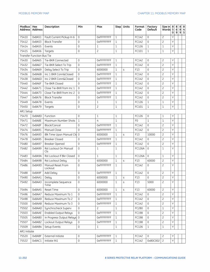
MODBUS MEMORY MAP CHAPTER 11: MODBUS MEMORY MAP
75410 0x8A51 Fault Current Pickup In 6 0 0xFFFFFFFF 1 FC142 0 2 Y
75412 0x8A53 Block Transfer 0 0xFFFFFFFF 1 FC142 0 2 Y
75414 0x8A55 Events 0 1 1 FC126 1 1 Y
75415 0x8A56 Targets 0 2 1 FC101 1 1 Y
Transfer Function Bus Tie
75430 0x8A65 Tie-BKR Connected 0 0xFFFFFFFF 1 FC142 0 2 Y
75432 0x8A67 Tie-BKR Select To Trip 0 0xFFFFFFFF 1 FC142 0 2 Y
75434 0x8A69 Delay Select To Trip 0 6000000 1 s F13 0 2 Y
75436 0x8A6B Inc 1 BKR Conn&Closed 0 0xFFFFFFFF 1 FC142 0 2 Y
75438 0x8A6D Inc 2 BKR Conn&Closed 0 0xFFFFFFFF 1 FC142 0 2 Y
75440 0x8A6F Tie-BKR Closed 0 0xFFFFFFFF 1 FC142 0 2 Y
75442 0x8A71 Close Tie-BKR from Inc 1 0 0xFFFFFFFF 1 FC142 0 2 Y
75444 0x8A73 Close Tie-BKR from Inc 2 0 0xFFFFFFFF 1 FC142 0 2 Y
75447 0x8A76 Block Transfer 0 0xFFFFFFFF 1 FC142 0 2 Y
75449 0x8A78 Events 0 1 1 FC126 1 1 Y
75450 0x8A79 Targets 0 2 1 FC101 1 1 Y
AR1 Setup
75470 0x8A8D Function 0 1 1 FC126 0 1 Y
75471 0x8A8E Maximum Number Shots 1 4 1 F0 1 1 Y
75472 0x8A8F Block/Cancel 0 0xFFFFFFFF 1 FC142 0 2 Y
75474 0x8A91 Manual Close 0 0xFFFFFFFF 1 FC142 0 2 Y
75476 0x8A93 Blk Time Upon Manual Cls 0 6000000 1 s F13 10000 2 Y
75478 0x8A95 Breaker Closed 0 0xFFFFFFFF 1 FC142 0 2 Y
75480 0x8A97 Breaker Opened 0 0xFFFFFFFF 1 FC142 0 2 Y
75482 0x8A99 Rst Lockout On Manual Cls
0 1 1 FC126A 0 1 Y
75483 0x8A9A Rst Lockout If Bkr Closed 0 1 1 FC126A 0 1 Y
75484 0x8A9B Rst Lockout Delay 0 6000000 1 s F13 60000 2 Y
75486 0x8A9D Manual Reset From Lockout
0 0xFFFFFFFF 1 FC142 0 2 Y
75488 0x8A9F Add Delay 0 0xFFFFFFFF 1 FC142 0 2 Y
75490 0x8AA1 Delay 0 6000000 1 s F13 0 2 Y
75492 0x8AA3 Incomplete Sequence Time
0 6000000 1 s F13 5000 2 Y
75494 0x8AA5 Reset Time 0 6000000 1 s F13 60000 2 Y
75496 0x8AA7 Reduce Maximum To 1 0 0xFFFFFFFF 1 FC142 0 2 Y
75498 0x8AA9 Reduce Maximum To 2 0 0xFFFFFFFF 1 FC142 0 2 Y
75500 0x8AAB Reduce Maximum To 3 0 0xFFFFFFFF 1 FC142 0 2 Y
75502 0x8AAD Synchrocheck Superv 0 2 1 FC280 0 1 Y
75503 0x8AAE Enabled Output Relays 0 0xFFFFFFFF 1 FC198 0 2 Y
75505 0x8AB0 In Progress Output Relays 0 0xFFFFFFFF 1 FC198 0 2 Y
75507 0x8AB2 Lockout Output Relays 0 0xFFFFFFFF 1 FC198 0 2 Y
75509 0x8AB4 Setup Events 0 1 1 FC126 1 1 Y
AR1 Initiate
75520 0x8ABF External Initiate 0 0xFFFFFFFF 1 FC142 0 2 Y
75522 0x8AC1 Initiate IN1 0 0xFFFFFFFF 1 FC142 0x80C002 2 Y
Modbus Address
Hex Address
Description Min Max Step Units Format Code
Factory Default
Size in Words
850
869
889
845
11-202 8 SERIES PROTECTIVE RELAY PLATFORM – COMMUNICATIONS GUIDE
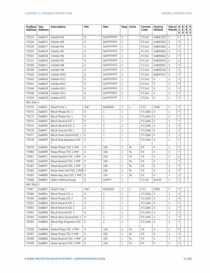
CHAPTER 11: MODBUS MEMORY MAP MODBUS MEMORY MAP
75524 0x8AC3 Initiate IN2 0 0xFFFFFFFF 1 FC142 0x80C202 2 Y
75526 0x8AC5 Initiate IN3 0 0xFFFFFFFF 1 FC142 0x80C602 2 Y
75528 0x8AC7 Initiate IN4 0 0xFFFFFFFF 1 FC142 0x80C802 2 Y
75530 0x8AC9 Initiate IN5 0 0xFFFFFFFF 1 FC142 0x80D802 2 Y
75532 0x8ACB Initiate IN6 0 0xFFFFFFFF 1 FC142 0x80DA02 2 Y
75534 0x8ACD Initiate IN7 0 0xFFFFFFFF 1 FC142 0x80DE02 2 Y
75536 0x8ACF Initiate IN8 0 0xFFFFFFFF 1 FC142 0x80E002 2 Y
75538 0x8AD1 Initiate IN9 0 0xFFFFFFFF 1 FC142 0x80EC02 2 Y
75540 0x8AD3 Initiate IN10 0 0xFFFFFFFF 1 FC142 0x80F202 2 Y
75542 0x8AD5 Initiate IN11 0 0xFFFFFFFF 1 FC142 0 2 Y
75544 0x8AD7 Initiate IN12 0 0xFFFFFFFF 1 FC142 0 2 Y
75546 0x8AD9 Initiate IN13 0 0xFFFFFFFF 1 FC142 0 2 Y
75548 0x8ADB Initiate IN14 0 0xFFFFFFFF 1 FC142 0 2 Y
75550 0x8ADD Initiate IN15 0 0xFFFFFFFF 1 FC142 0 2 Y
AR1 Shot 1
75570 0x8AF1 Dead Time 1 100 6000000 1 s F13 1000 2 Y
75572 0x8AF3 Block Phase IOC 1 0 1 1 FC126A 0 1 Y
75573 0x8AF4 Block Phase IOC 2 0 1 1 FC126A 0 1 Y
75574 0x8AF5 Block Neutral IOC 1 0 1 1 FC126A 0 1 Y
75575 0x8AF6 Block Neutral IOC 2 0 1 1 FC126A 0 1 Y
75576 0x8AF7 Block Ground IOC 1 0 1 1 FC126A 0 1 Y
75577 0x8AF8 Block Sens Ground IOC 1 0 1 1 FC126A 0 1 Y
75578 0x8AF9 Block Neg Sequence IOC 1
0 1 1 FC126A 0 1 Y
75579 0x8AFA Raise Phase TOC 1 PKP 0 100 1 % F0 0 1 Y
75580 0x8AFB Raise Phase TOC 2 PKP 0 100 1 % F0 0 1 Y
75581 0x8AFC Raise Neutral TOC 1 PKP 0 100 1 % F0 0 1 Y
75582 0x8AFD Raise Neutral TOC 2 PKP 0 100 1 % F0 0 1 Y
75583 0x8AFE Raise Ground TOC 1 PKP 0 100 1 % F0 0 1 Y
75584 0x8AFF Raise Sens Gnd TOC 1 PKP 0 100 1 % F0 0 1 Y
75585 0x8B00 Raise Neg Seq TOC 1 PKP 0 100 1 % F0 0 1 Y
75586 0x8B01 Select Setting Group 0 0xFFFF 1 FC132 65535 1 Y
AR1 Shot 2
75587 0x8B02 Dead Time 2 100 6000000 1 s F13 2000 2 Y
75589 0x8B04 Block Phase IOC 1 0 1 1 FC126A 0 1 Y
75590 0x8B05 Block Phase IOC 2 0 1 1 FC126A 0 1 Y
75591 0x8B06 Block Neutral IOC 1 0 1 1 FC126A 0 1 Y
75592 0x8B07 Block Neutral IOC 2 0 1 1 FC126A 0 1 Y
75593 0x8B08 Block Ground IOC 1 0 1 1 FC126A 0 1 Y
75594 0x8B09 Block Sens Ground IOC 1 0 1 1 FC126A 0 1 Y
75595 0x8B0A Block Neg Sequence IOC 1
0 1 1 FC126A 0 1 Y
75596 0x8B0B Raise Phase TOC 1 PKP 0 100 1 % F0 0 1 Y
75597 0x8B0C Raise Phase TOC 2 PKP 0 100 1 % F0 0 1 Y
75598 0x8B0D Raise Neutral TOC 1 PKP 0 100 1 % F0 0 1 Y
75599 0x8B0E Raise Neutral TOC 2 PKP 0 100 1 % F0 0 1 Y
Modbus Address
Hex Address
Description Min Max Step Units Format Code
Factory Default
Size in Words
850
869
889
845
8 SERIES PROTECTIVE RELAY PLATFORM – COMMUNICATIONS GUIDE 11-203
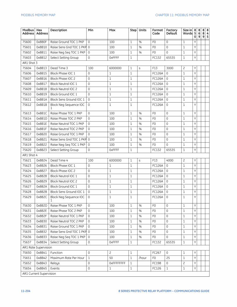
MODBUS MEMORY MAP CHAPTER 11: MODBUS MEMORY MAP
75600 0x8B0F Raise Ground TOC 1 PKP 0 100 1 % F0 0 1 Y
75601 0x8B10 Raise Sens Gnd TOC 1 PKP 0 100 1 % F0 0 1 Y
75602 0x8B11 Raise Neg Seq TOC 1 PKP 0 100 1 % F0 0 1 Y
75603 0x8B12 Select Setting Group 0 0xFFFF 1 FC132 65535 1 Y
AR1 Shot 3
75604 0x8B13 Dead Time 3 100 6000000 1 s F13 3000 2 Y
75606 0x8B15 Block Phase IOC 1 0 1 1 FC126A 0 1 Y
75607 0x8B16 Block Phase IOC 2 0 1 1 FC126A 0 1 Y
75608 0x8B17 Block Neutral IOC 1 0 1 1 FC126A 0 1 Y
75609 0x8B18 Block Neutral IOC 2 0 1 1 FC126A 0 1 Y
75610 0x8B19 Block Ground IOC 1 0 1 1 FC126A 0 1 Y
75611 0x8B1A Block Sens Ground IOC 1 0 1 1 FC126A 0 1 Y
75612 0x8B1B Block Neg Sequence IOC 1
0 1 1 FC126A 0 1 Y
75613 0x8B1C Raise Phase TOC 1 PKP 0 100 1 % F0 0 1 Y
75614 0x8B1D Raise Phase TOC 2 PKP 0 100 1 % F0 0 1 Y
75615 0x8B1E Raise Neutral TOC 1 PKP 0 100 1 % F0 0 1 Y
75616 0x8B1F Raise Neutral TOC 2 PKP 0 100 1 % F0 0 1 Y
75617 0x8B20 Raise Ground TOC 1 PKP 0 100 1 % F0 0 1 Y
75618 0x8B21 Raise Sens Gnd TOC 1 PKP 0 100 1 % F0 0 1 Y
75619 0x8B22 Raise Neg Seq TOC 1 PKP 0 100 1 % F0 0 1 Y
75620 0x8B23 Select Setting Group 0 0xFFFF 1 FC132 65535 1 Y
AR1 Shot 4
75621 0x8B24 Dead Time 4 100 6000000 1 s F13 4000 2 Y
75623 0x8B26 Block Phase IOC 1 0 1 1 FC126A 0 1 Y
75624 0x8B27 Block Phase IOC 2 0 1 1 FC126A 0 1 Y
75625 0x8B28 Block Neutral IOC 1 0 1 1 FC126A 0 1 Y
75626 0x8B29 Block Neutral IOC 2 0 1 1 FC126A 0 1 Y
75627 0x8B2A Block Ground IOC 1 0 1 1 FC126A 0 1 Y
75628 0x8B2B Block Sens Ground IOC 1 0 1 1 FC126A 0 1 Y
75629 0x8B2C Block Neg Sequence IOC 1
0 1 1 FC126A 0 1 Y
75630 0x8B2D Raise Phase TOC 1 PKP 0 100 1 % F0 0 1 Y
75631 0x8B2E Raise Phase TOC 2 PKP 0 100 1 % F0 0 1 Y
75632 0x8B2F Raise Neutral TOC 1 PKP 0 100 1 % F0 0 1 Y
75633 0x8B30 Raise Neutral TOC 2 PKP 0 100 1 % F0 0 1 Y
75634 0x8B31 Raise Ground TOC 1 PKP 0 100 1 % F0 0 1 Y
75635 0x8B32 Raise Sens Gnd TOC 1 PKP 0 100 1 % F0 0 1 Y
75636 0x8B33 Raise Neg Seq TOC 1 PKP 0 100 1 % F0 0 1 Y
75637 0x8B34 Select Setting Group 0 0xFFFF 1 FC132 65535 1 Y
AR1 Rate Supervision
75650 0x8B41 Function 0 2 1 FC267 0 1 Y
75651 0x8B42 Maximum Rate Per Hour 1 50 1 /hour F0 25 1 Y
75652 0x8B43 Relays 0 0xFFFFFFFF 1 FC198 0 2 Y
75654 0x8B45 Events 0 1 1 FC126 1 1 Y
AR1 Current Supervision
Modbus Address
Hex Address
Description Min Max Step Units Format Code
Factory Default
Size in Words
850
869
889
845
11-204 8 SERIES PROTECTIVE RELAY PLATFORM – COMMUNICATIONS GUIDE

CHAPTER 11: MODBUS MEMORY MAP MODBUS MEMORY MAP
75670 0x8B55 Function 0 1 1 FC126 0 1 Y
75672 0x8B57 3 Shots For Current Above 50 30000 1 x CT F13 17000 2 Y
75674 0x8B59 2 Shots For Current Above 50 30000 1 x CT F13 18000 2 Y
75676 0x8B5B 1 Shots For Current Above 50 30000 1 x CT F13 19000 2 Y
75678 0x8B5D Lockout For Current Above
50 30000 1 x CT F13 20000 2 Y
75680 0x8B5F Lockout 0 1 1 FC126 0 1 Y
75681 0x8B60 Events 0 1 1 FC126 1 1 Y
AR1 Zone Coordination
75700 0x8B73 Function 0 1 1 FC126 0 1 Y
75702 0x8B75 Phase Current Pickup 50 30000 1 x CT F13 1000 2 Y
75704 0x8B77 Neutral Current Pickup 50 30000 1 x CT F13 300 2 Y
75706 0x8B79 Pickup Time 0 6000000 1 s F13 20 2 Y
75708 0x8B7B Dropout Time 0 6000000 1 s F13 20 2 Y
75710 0x8B7D Events 0 1 1 FC126 1 1 Y
VT Fuse Fail 1
75990 0x8C95 Name 0 65535 1 F60_26 VT Fuse Fail1
13 Y Y Y Y
76003 0x8CA2 Function 0 4 1 FC100A 0 1 Y Y Y Y
76005 0x8CA4 Relays 0 0xFFFFFFFF 1 FC198 0 2 Y Y Y Y
76007 0x8CA6 Events 0 1 1 FC126 1 1 Y Y Y Y
76008 0x8CA7 Targets 0 2 1 FC101 1 1 Y Y Y Y
VT Fuse Fail 2
76015 0x8CAE Name 0 65535 1 F60_26 VT Fuse Fail2
13 Y
76028 0x8CBB Function 0 4 1 FC100A 0 1 Y
76030 0x8CBD Relays 0 0xFFFFFFFF 1 FC198 0 2 Y
76032 0x8CBF Events 0 1 1 FC126 1 1 Y
76033 0x8CC0 Targets 0 2 1 FC101 1 1 Y
Arc Flash 1
76050 0x8CD1 Function 0 4 1 FC100 0 1 Y Y Y Y
76051 0x8CD2 Signal Input 1 4 1 FC102A 1 1 Y Y
76052 0x8CD3 HS Phase Pickup 50 30000 1 x CT F3 2000 1 Y Y Y Y
76053 0x8CD4 HS Ground Pickup 50 30000 1 x CT F3 1000 1 Y Y Y Y
76054 0x8CD5 Light Sensor 1 0 1 1 FC126 0 1 Y Y Y Y
76055 0x8CD6 Light Sensor 2 0 1 1 FC126 0 1 Y Y Y Y
76056 0x8CD7 Light Sensor 3 0 1 1 FC126 0 1 Y Y Y Y
76057 0x8CD8 Light Sensor 4 0 1 1 FC126 0 1 Y Y Y Y
76070 0x8CE5 Block 0 0xFFFFFFFF 1 FC142 0 2 Y Y Y Y
76072 0x8CE7 Trip Output Relay 0 0xFFFFFFFF 1 FC198 0 2 Y Y Y Y
76074 0x8CE9 Events 0 1 1 FC126 1 1 Y Y Y Y
76075 0x8CEA Targets 0 2 1 FC101 2 1 Y Y Y Y
W1 Harmonic Derating
80000 0x9C3F Function 0 4 1 FC100A 0 1 Y
80001 0x9C40 Minimum Oper Current 3 100 1 x CT F2 10 1 Y
80002 0x9C41 Pickup 1 98 1 F2 90 1 Y
Modbus Address
Hex Address
Description Min Max Step Units Format Code
Factory Default
Size in Words
850
869
889
845
8 SERIES PROTECTIVE RELAY PLATFORM – COMMUNICATIONS GUIDE 11-205
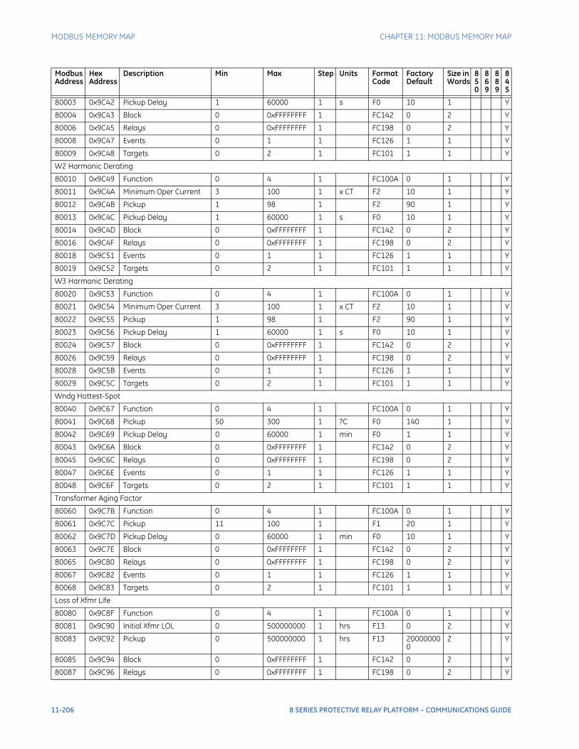
MODBUS MEMORY MAP CHAPTER 11: MODBUS MEMORY MAP
80003 0x9C42 Pickup Delay 1 60000 1 s F0 10 1 Y
80004 0x9C43 Block 0 0xFFFFFFFF 1 FC142 0 2 Y
80006 0x9C45 Relays 0 0xFFFFFFFF 1 FC198 0 2 Y
80008 0x9C47 Events 0 1 1 FC126 1 1 Y
80009 0x9C48 Targets 0 2 1 FC101 1 1 Y
W2 Harmonic Derating
80010 0x9C49 Function 0 4 1 FC100A 0 1 Y
80011 0x9C4A Minimum Oper Current 3 100 1 x CT F2 10 1 Y
80012 0x9C4B Pickup 1 98 1 F2 90 1 Y
80013 0x9C4C Pickup Delay 1 60000 1 s F0 10 1 Y
80014 0x9C4D Block 0 0xFFFFFFFF 1 FC142 0 2 Y
80016 0x9C4F Relays 0 0xFFFFFFFF 1 FC198 0 2 Y
80018 0x9C51 Events 0 1 1 FC126 1 1 Y
80019 0x9C52 Targets 0 2 1 FC101 1 1 Y
W3 Harmonic Derating
80020 0x9C53 Function 0 4 1 FC100A 0 1 Y
80021 0x9C54 Minimum Oper Current 3 100 1 x CT F2 10 1 Y
80022 0x9C55 Pickup 1 98 1 F2 90 1 Y
80023 0x9C56 Pickup Delay 1 60000 1 s F0 10 1 Y
80024 0x9C57 Block 0 0xFFFFFFFF 1 FC142 0 2 Y
80026 0x9C59 Relays 0 0xFFFFFFFF 1 FC198 0 2 Y
80028 0x9C5B Events 0 1 1 FC126 1 1 Y
80029 0x9C5C Targets 0 2 1 FC101 1 1 Y
Wndg Hottest-Spot
80040 0x9C67 Function 0 4 1 FC100A 0 1 Y
80041 0x9C68 Pickup 50 300 1 ?C F0 140 1 Y
80042 0x9C69 Pickup Delay 0 60000 1 min F0 1 1 Y
80043 0x9C6A Block 0 0xFFFFFFFF 1 FC142 0 2 Y
80045 0x9C6C Relays 0 0xFFFFFFFF 1 FC198 0 2 Y
80047 0x9C6E Events 0 1 1 FC126 1 1 Y
80048 0x9C6F Targets 0 2 1 FC101 1 1 Y
Transformer Aging Factor
80060 0x9C7B Function 0 4 1 FC100A 0 1 Y
80061 0x9C7C Pickup 11 100 1 F1 20 1 Y
80062 0x9C7D Pickup Delay 0 60000 1 min F0 10 1 Y
80063 0x9C7E Block 0 0xFFFFFFFF 1 FC142 0 2 Y
80065 0x9C80 Relays 0 0xFFFFFFFF 1 FC198 0 2 Y
80067 0x9C82 Events 0 1 1 FC126 1 1 Y
80068 0x9C83 Targets 0 2 1 FC101 1 1 Y
Loss of Xfmr Life
80080 0x9C8F Function 0 4 1 FC100A 0 1 Y
80081 0x9C90 Initial Xfmr LOL 0 500000000 1 hrs F13 0 2 Y
80083 0x9C92 Pickup 0 500000000 1 hrs F13 200000000
2 Y
80085 0x9C94 Block 0 0xFFFFFFFF 1 FC142 0 2 Y
80087 0x9C96 Relays 0 0xFFFFFFFF 1 FC198 0 2 Y
Modbus Address
Hex Address
Description Min Max Step Units Format Code
Factory Default
Size in Words
850
869
889
845
11-206 8 SERIES PROTECTIVE RELAY PLATFORM – COMMUNICATIONS GUIDE
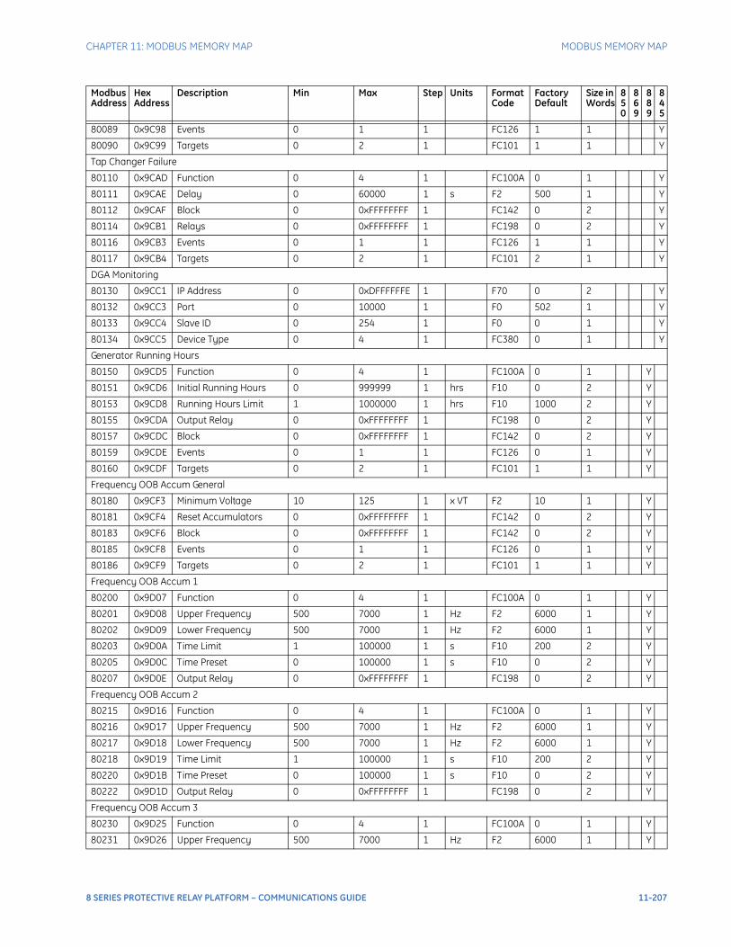
CHAPTER 11: MODBUS MEMORY MAP MODBUS MEMORY MAP
80089 0x9C98 Events 0 1 1 FC126 1 1 Y
80090 0x9C99 Targets 0 2 1 FC101 1 1 Y
Tap Changer Failure
80110 0x9CAD Function 0 4 1 FC100A 0 1 Y
80111 0x9CAE Delay 0 60000 1 s F2 500 1 Y
80112 0x9CAF Block 0 0xFFFFFFFF 1 FC142 0 2 Y
80114 0x9CB1 Relays 0 0xFFFFFFFF 1 FC198 0 2 Y
80116 0x9CB3 Events 0 1 1 FC126 1 1 Y
80117 0x9CB4 Targets 0 2 1 FC101 2 1 Y
DGA Monitoring
80130 0x9CC1 IP Address 0 0xDFFFFFFE 1 F70 0 2 Y
80132 0x9CC3 Port 0 10000 1 F0 502 1 Y
80133 0x9CC4 Slave ID 0 254 1 F0 0 1 Y
80134 0x9CC5 Device Type 0 4 1 FC380 0 1 Y
Generator Running Hours
80150 0x9CD5 Function 0 4 1 FC100A 0 1 Y
80151 0x9CD6 Initial Running Hours 0 999999 1 hrs F10 0 2 Y
80153 0x9CD8 Running Hours Limit 1 1000000 1 hrs F10 1000 2 Y
80155 0x9CDA Output Relay 0 0xFFFFFFFF 1 FC198 0 2 Y
80157 0x9CDC Block 0 0xFFFFFFFF 1 FC142 0 2 Y
80159 0x9CDE Events 0 1 1 FC126 0 1 Y
80160 0x9CDF Targets 0 2 1 FC101 1 1 Y
Frequency OOB Accum General
80180 0x9CF3 Minimum Voltage 10 125 1 x VT F2 10 1 Y
80181 0x9CF4 Reset Accumulators 0 0xFFFFFFFF 1 FC142 0 2 Y
80183 0x9CF6 Block 0 0xFFFFFFFF 1 FC142 0 2 Y
80185 0x9CF8 Events 0 1 1 FC126 0 1 Y
80186 0x9CF9 Targets 0 2 1 FC101 1 1 Y
Frequency OOB Accum 1
80200 0x9D07 Function 0 4 1 FC100A 0 1 Y
80201 0x9D08 Upper Frequency 500 7000 1 Hz F2 6000 1 Y
80202 0x9D09 Lower Frequency 500 7000 1 Hz F2 6000 1 Y
80203 0x9D0A Time Limit 1 100000 1 s F10 200 2 Y
80205 0x9D0C Time Preset 0 100000 1 s F10 0 2 Y
80207 0x9D0E Output Relay 0 0xFFFFFFFF 1 FC198 0 2 Y
Frequency OOB Accum 2
80215 0x9D16 Function 0 4 1 FC100A 0 1 Y
80216 0x9D17 Upper Frequency 500 7000 1 Hz F2 6000 1 Y
80217 0x9D18 Lower Frequency 500 7000 1 Hz F2 6000 1 Y
80218 0x9D19 Time Limit 1 100000 1 s F10 200 2 Y
80220 0x9D1B Time Preset 0 100000 1 s F10 0 2 Y
80222 0x9D1D Output Relay 0 0xFFFFFFFF 1 FC198 0 2 Y
Frequency OOB Accum 3
80230 0x9D25 Function 0 4 1 FC100A 0 1 Y
80231 0x9D26 Upper Frequency 500 7000 1 Hz F2 6000 1 Y
Modbus Address
Hex Address
Description Min Max Step Units Format Code
Factory Default
Size in Words
850
869
889
845
8 SERIES PROTECTIVE RELAY PLATFORM – COMMUNICATIONS GUIDE 11-207
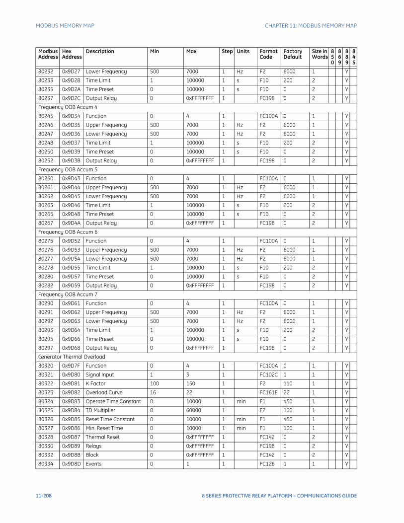
MODBUS MEMORY MAP CHAPTER 11: MODBUS MEMORY MAP
80232 0x9D27 Lower Frequency 500 7000 1 Hz F2 6000 1 Y
80233 0x9D28 Time Limit 1 100000 1 s F10 200 2 Y
80235 0x9D2A Time Preset 0 100000 1 s F10 0 2 Y
80237 0x9D2C Output Relay 0 0xFFFFFFFF 1 FC198 0 2 Y
Frequency OOB Accum 4
80245 0x9D34 Function 0 4 1 FC100A 0 1 Y
80246 0x9D35 Upper Frequency 500 7000 1 Hz F2 6000 1 Y
80247 0x9D36 Lower Frequency 500 7000 1 Hz F2 6000 1 Y
80248 0x9D37 Time Limit 1 100000 1 s F10 200 2 Y
80250 0x9D39 Time Preset 0 100000 1 s F10 0 2 Y
80252 0x9D3B Output Relay 0 0xFFFFFFFF 1 FC198 0 2 Y
Frequency OOB Accum 5
80260 0x9D43 Function 0 4 1 FC100A 0 1 Y
80261 0x9D44 Upper Frequency 500 7000 1 Hz F2 6000 1 Y
80262 0x9D45 Lower Frequency 500 7000 1 Hz F2 6000 1 Y
80263 0x9D46 Time Limit 1 100000 1 s F10 200 2 Y
80265 0x9D48 Time Preset 0 100000 1 s F10 0 2 Y
80267 0x9D4A Output Relay 0 0xFFFFFFFF 1 FC198 0 2 Y
Frequency OOB Accum 6
80275 0x9D52 Function 0 4 1 FC100A 0 1 Y
80276 0x9D53 Upper Frequency 500 7000 1 Hz F2 6000 1 Y
80277 0x9D54 Lower Frequency 500 7000 1 Hz F2 6000 1 Y
80278 0x9D55 Time Limit 1 100000 1 s F10 200 2 Y
80280 0x9D57 Time Preset 0 100000 1 s F10 0 2 Y
80282 0x9D59 Output Relay 0 0xFFFFFFFF 1 FC198 0 2 Y
Frequency OOB Accum 7
80290 0x9D61 Function 0 4 1 FC100A 0 1 Y
80291 0x9D62 Upper Frequency 500 7000 1 Hz F2 6000 1 Y
80292 0x9D63 Lower Frequency 500 7000 1 Hz F2 6000 1 Y
80293 0x9D64 Time Limit 1 100000 1 s F10 200 2 Y
80295 0x9D66 Time Preset 0 100000 1 s F10 0 2 Y
80297 0x9D68 Output Relay 0 0xFFFFFFFF 1 FC198 0 2 Y
Generator Thermal Overload
80320 0x9D7F Function 0 4 1 FC100A 0 1 Y
80321 0x9D80 Signal Input 1 3 1 FC102C 1 1 Y
80322 0x9D81 K Factor 100 150 1 F2 110 1 Y
80323 0x9D82 Overload Curve 16 22 1 FC161E 22 1 Y
80324 0x9D83 Operate Time Constant 0 10000 1 min F1 450 1 Y
80325 0x9D84 TD Multiplier 0 60000 1 F2 100 1 Y
80326 0x9D85 Reset Time Constant 0 10000 1 min F1 450 1 Y
80327 0x9D86 Min. Reset Time 0 10000 1 min F1 100 1 Y
80328 0x9D87 Thermal Reset 0 0xFFFFFFFF 1 FC142 0 2 Y
80330 0x9D89 Relays 0 0xFFFFFFFF 1 FC198 0 2 Y
80332 0x9D8B Block 0 0xFFFFFFFF 1 FC142 0 2 Y
80334 0x9D8D Events 0 1 1 FC126 1 1 Y
Modbus Address
Hex Address
Description Min Max Step Units Format Code
Factory Default
Size in Words
850
869
889
845
11-208 8 SERIES PROTECTIVE RELAY PLATFORM – COMMUNICATIONS GUIDE
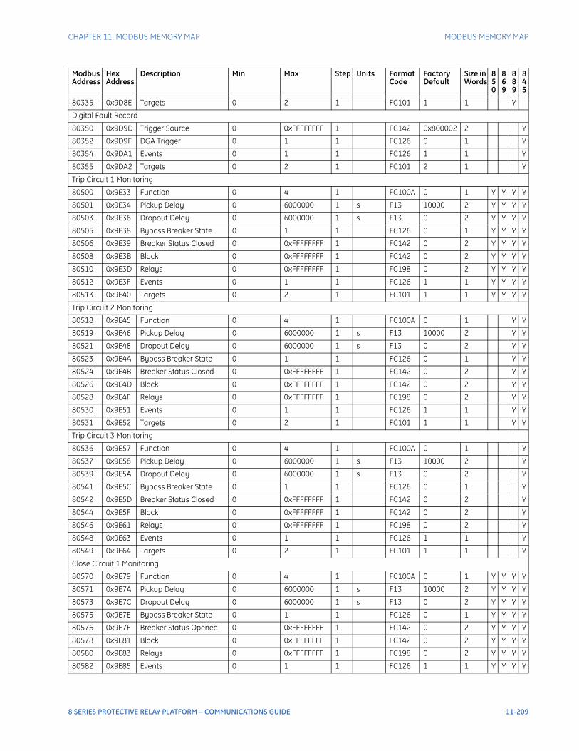
CHAPTER 11: MODBUS MEMORY MAP MODBUS MEMORY MAP
80335 0x9D8E Targets 0 2 1 FC101 1 1 Y
Digital Fault Record
80350 0x9D9D Trigger Source 0 0xFFFFFFFF 1 FC142 0x800002 2 Y
80352 0x9D9F DGA Trigger 0 1 1 FC126 0 1 Y
80354 0x9DA1 Events 0 1 1 FC126 1 1 Y
80355 0x9DA2 Targets 0 2 1 FC101 2 1 Y
Trip Circuit 1 Monitoring
80500 0x9E33 Function 0 4 1 FC100A 0 1 Y Y Y Y
80501 0x9E34 Pickup Delay 0 6000000 1 s F13 10000 2 Y Y Y Y
80503 0x9E36 Dropout Delay 0 6000000 1 s F13 0 2 Y Y Y Y
80505 0x9E38 Bypass Breaker State 0 1 1 FC126 0 1 Y Y Y Y
80506 0x9E39 Breaker Status Closed 0 0xFFFFFFFF 1 FC142 0 2 Y Y Y Y
80508 0x9E3B Block 0 0xFFFFFFFF 1 FC142 0 2 Y Y Y Y
80510 0x9E3D Relays 0 0xFFFFFFFF 1 FC198 0 2 Y Y Y Y
80512 0x9E3F Events 0 1 1 FC126 1 1 Y Y Y Y
80513 0x9E40 Targets 0 2 1 FC101 1 1 Y Y Y Y
Trip Circuit 2 Monitoring
80518 0x9E45 Function 0 4 1 FC100A 0 1 Y Y
80519 0x9E46 Pickup Delay 0 6000000 1 s F13 10000 2 Y Y
80521 0x9E48 Dropout Delay 0 6000000 1 s F13 0 2 Y Y
80523 0x9E4A Bypass Breaker State 0 1 1 FC126 0 1 Y Y
80524 0x9E4B Breaker Status Closed 0 0xFFFFFFFF 1 FC142 0 2 Y Y
80526 0x9E4D Block 0 0xFFFFFFFF 1 FC142 0 2 Y Y
80528 0x9E4F Relays 0 0xFFFFFFFF 1 FC198 0 2 Y Y
80530 0x9E51 Events 0 1 1 FC126 1 1 Y Y
80531 0x9E52 Targets 0 2 1 FC101 1 1 Y Y
Trip Circuit 3 Monitoring
80536 0x9E57 Function 0 4 1 FC100A 0 1 Y
80537 0x9E58 Pickup Delay 0 6000000 1 s F13 10000 2 Y
80539 0x9E5A Dropout Delay 0 6000000 1 s F13 0 2 Y
80541 0x9E5C Bypass Breaker State 0 1 1 FC126 0 1 Y
80542 0x9E5D Breaker Status Closed 0 0xFFFFFFFF 1 FC142 0 2 Y
80544 0x9E5F Block 0 0xFFFFFFFF 1 FC142 0 2 Y
80546 0x9E61 Relays 0 0xFFFFFFFF 1 FC198 0 2 Y
80548 0x9E63 Events 0 1 1 FC126 1 1 Y
80549 0x9E64 Targets 0 2 1 FC101 1 1 Y
Close Circuit 1 Monitoring
80570 0x9E79 Function 0 4 1 FC100A 0 1 Y Y Y Y
80571 0x9E7A Pickup Delay 0 6000000 1 s F13 10000 2 Y Y Y Y
80573 0x9E7C Dropout Delay 0 6000000 1 s F13 0 2 Y Y Y Y
80575 0x9E7E Bypass Breaker State 0 1 1 FC126 0 1 Y Y Y Y
80576 0x9E7F Breaker Status Opened 0 0xFFFFFFFF 1 FC142 0 2 Y Y Y Y
80578 0x9E81 Block 0 0xFFFFFFFF 1 FC142 0 2 Y Y Y Y
80580 0x9E83 Relays 0 0xFFFFFFFF 1 FC198 0 2 Y Y Y Y
80582 0x9E85 Events 0 1 1 FC126 1 1 Y Y Y Y
Modbus Address
Hex Address
Description Min Max Step Units Format Code
Factory Default
Size in Words
850
869
889
845
8 SERIES PROTECTIVE RELAY PLATFORM – COMMUNICATIONS GUIDE 11-209
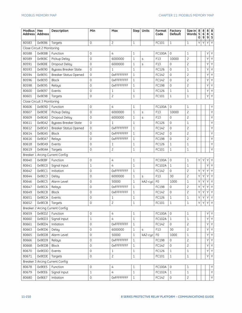
MODBUS MEMORY MAP CHAPTER 11: MODBUS MEMORY MAP
80583 0x9E86 Targets 0 2 1 FC101 1 1 Y Y Y Y
Close Circuit 2 Monitoring
80588 0x9E8B Function 0 4 1 FC100A 0 1 Y Y
80589 0x9E8C Pickup Delay 0 6000000 1 s F13 10000 2 Y Y
80591 0x9E8E Dropout Delay 0 6000000 1 s F13 0 2 Y Y
80593 0x9E90 Bypass Breaker State 0 1 1 FC126 0 1 Y Y
80594 0x9E91 Breaker Status Opened 0 0xFFFFFFFF 1 FC142 0 2 Y Y
80596 0x9E93 Block 0 0xFFFFFFFF 1 FC142 0 2 Y Y
80598 0x9E95 Relays 0 0xFFFFFFFF 1 FC198 0 2 Y Y
80600 0x9E97 Events 0 1 1 FC126 1 1 Y Y
80601 0x9E98 Targets 0 2 1 FC101 1 1 Y Y
Close Circuit 3 Monitoring
80606 0x9E9D Function 0 4 1 FC100A 0 1 Y
80607 0x9E9E Pickup Delay 0 6000000 1 s F13 10000 2 Y
80609 0x9EA0 Dropout Delay 0 6000000 1 s F13 0 2 Y
80611 0x9EA2 Bypass Breaker State 0 1 1 FC126 0 1 Y
80612 0x9EA3 Breaker Status Opened 0 0xFFFFFFFF 1 FC142 0 2 Y
80614 0x9EA5 Block 0 0xFFFFFFFF 1 FC142 0 2 Y
80616 0x9EA7 Relays 0 0xFFFFFFFF 1 FC198 0 2 Y
80618 0x9EA9 Events 0 1 1 FC126 1 1 Y
80619 0x9EAA Targets 0 2 1 FC101 1 1 Y
Breaker 1 Arcing Current Config
80640 0x9EBF Function 0 4 1 FC100A 0 1 Y Y Y Y
80641 0x9EC0 Signal Input 1 4 1 FC102A 1 1 Y Y
80642 0x9EC1 Initiation 0 0xFFFFFFFF 1 FC142 0 2 Y Y Y Y
80644 0x9EC3 Delay 0 6000000 1 s F13 30 2 Y Y Y Y
80646 0x9EC5 Alarm Level 0 50000 1 kA2-cyc F0 1000 1 Y Y Y Y
80647 0x9EC6 Relays 0 0xFFFFFFFF 1 FC198 0 2 Y Y Y Y
80649 0x9EC8 Block 0 0xFFFFFFFF 1 FC142 0 2 Y Y Y Y
80651 0x9ECA Events 0 1 1 FC126 1 1 Y Y Y Y
80652 0x9ECB Targets 0 2 1 FC101 1 1 Y Y Y Y
Breaker 2 Arcing Current Config
80659 0x9ED2 Function 0 4 1 FC100A 0 1 Y Y
80660 0x9ED3 Signal Input 1 4 1 FC102A 1 1 Y Y
80661 0x9ED4 Initiation 0 0xFFFFFFFF 1 FC142 0 2 Y Y
80663 0x9ED6 Delay 0 6000000 1 s F13 30 2 Y Y
80665 0x9ED8 Alarm Level 0 50000 1 kA2-cyc F0 1000 1 Y Y
80666 0x9ED9 Relays 0 0xFFFFFFFF 1 FC198 0 2 Y Y
80668 0x9EDB Block 0 0xFFFFFFFF 1 FC142 0 2 Y Y
80670 0x9EDD Events 0 1 1 FC126 1 1 Y Y
80671 0x9EDE Targets 0 2 1 FC101 1 1 Y Y
Breaker 3 Arcing Current Config
80678 0x9EE5 Function 0 4 1 FC100A 0 1 Y
80679 0x9EE6 Signal Input 1 4 1 FC102A 1 1 Y
80680 0x9EE7 Initiation 0 0xFFFFFFFF 1 FC142 0 2 Y
Modbus Address
Hex Address
Description Min Max Step Units Format Code
Factory Default
Size in Words
850
869
889
845
11-210 8 SERIES PROTECTIVE RELAY PLATFORM – COMMUNICATIONS GUIDE
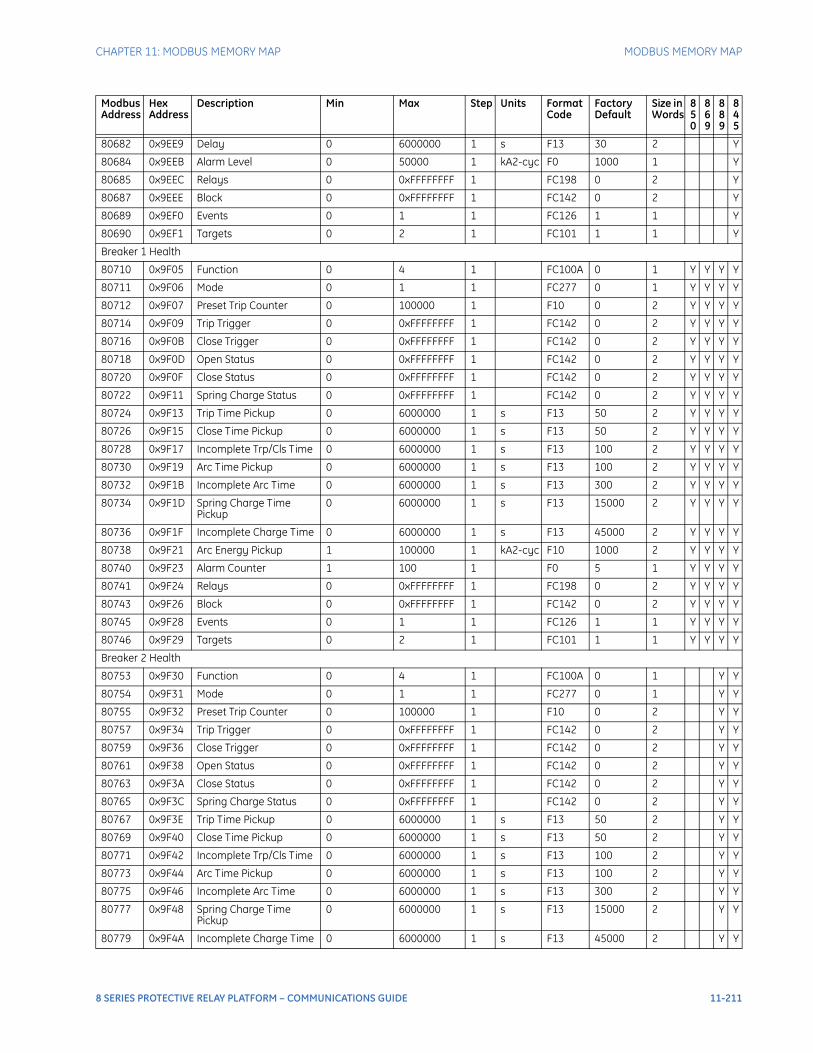
CHAPTER 11: MODBUS MEMORY MAP MODBUS MEMORY MAP
80682 0x9EE9 Delay 0 6000000 1 s F13 30 2 Y
80684 0x9EEB Alarm Level 0 50000 1 kA2-cyc F0 1000 1 Y
80685 0x9EEC Relays 0 0xFFFFFFFF 1 FC198 0 2 Y
80687 0x9EEE Block 0 0xFFFFFFFF 1 FC142 0 2 Y
80689 0x9EF0 Events 0 1 1 FC126 1 1 Y
80690 0x9EF1 Targets 0 2 1 FC101 1 1 Y
Breaker 1 Health
80710 0x9F05 Function 0 4 1 FC100A 0 1 Y Y Y Y
80711 0x9F06 Mode 0 1 1 FC277 0 1 Y Y Y Y
80712 0x9F07 Preset Trip Counter 0 100000 1 F10 0 2 Y Y Y Y
80714 0x9F09 Trip Trigger 0 0xFFFFFFFF 1 FC142 0 2 Y Y Y Y
80716 0x9F0B Close Trigger 0 0xFFFFFFFF 1 FC142 0 2 Y Y Y Y
80718 0x9F0D Open Status 0 0xFFFFFFFF 1 FC142 0 2 Y Y Y Y
80720 0x9F0F Close Status 0 0xFFFFFFFF 1 FC142 0 2 Y Y Y Y
80722 0x9F11 Spring Charge Status 0 0xFFFFFFFF 1 FC142 0 2 Y Y Y Y
80724 0x9F13 Trip Time Pickup 0 6000000 1 s F13 50 2 Y Y Y Y
80726 0x9F15 Close Time Pickup 0 6000000 1 s F13 50 2 Y Y Y Y
80728 0x9F17 Incomplete Trp/Cls Time 0 6000000 1 s F13 100 2 Y Y Y Y
80730 0x9F19 Arc Time Pickup 0 6000000 1 s F13 100 2 Y Y Y Y
80732 0x9F1B Incomplete Arc Time 0 6000000 1 s F13 300 2 Y Y Y Y
80734 0x9F1D Spring Charge Time Pickup
0 6000000 1 s F13 15000 2 Y Y Y Y
80736 0x9F1F Incomplete Charge Time 0 6000000 1 s F13 45000 2 Y Y Y Y
80738 0x9F21 Arc Energy Pickup 1 100000 1 kA2-cyc F10 1000 2 Y Y Y Y
80740 0x9F23 Alarm Counter 1 100 1 F0 5 1 Y Y Y Y
80741 0x9F24 Relays 0 0xFFFFFFFF 1 FC198 0 2 Y Y Y Y
80743 0x9F26 Block 0 0xFFFFFFFF 1 FC142 0 2 Y Y Y Y
80745 0x9F28 Events 0 1 1 FC126 1 1 Y Y Y Y
80746 0x9F29 Targets 0 2 1 FC101 1 1 Y Y Y Y
Breaker 2 Health
80753 0x9F30 Function 0 4 1 FC100A 0 1 Y Y
80754 0x9F31 Mode 0 1 1 FC277 0 1 Y Y
80755 0x9F32 Preset Trip Counter 0 100000 1 F10 0 2 Y Y
80757 0x9F34 Trip Trigger 0 0xFFFFFFFF 1 FC142 0 2 Y Y
80759 0x9F36 Close Trigger 0 0xFFFFFFFF 1 FC142 0 2 Y Y
80761 0x9F38 Open Status 0 0xFFFFFFFF 1 FC142 0 2 Y Y
80763 0x9F3A Close Status 0 0xFFFFFFFF 1 FC142 0 2 Y Y
80765 0x9F3C Spring Charge Status 0 0xFFFFFFFF 1 FC142 0 2 Y Y
80767 0x9F3E Trip Time Pickup 0 6000000 1 s F13 50 2 Y Y
80769 0x9F40 Close Time Pickup 0 6000000 1 s F13 50 2 Y Y
80771 0x9F42 Incomplete Trp/Cls Time 0 6000000 1 s F13 100 2 Y Y
80773 0x9F44 Arc Time Pickup 0 6000000 1 s F13 100 2 Y Y
80775 0x9F46 Incomplete Arc Time 0 6000000 1 s F13 300 2 Y Y
80777 0x9F48 Spring Charge Time Pickup
0 6000000 1 s F13 15000 2 Y Y
80779 0x9F4A Incomplete Charge Time 0 6000000 1 s F13 45000 2 Y Y
Modbus Address
Hex Address
Description Min Max Step Units Format Code
Factory Default
Size in Words
850
869
889
845
8 SERIES PROTECTIVE RELAY PLATFORM – COMMUNICATIONS GUIDE 11-211
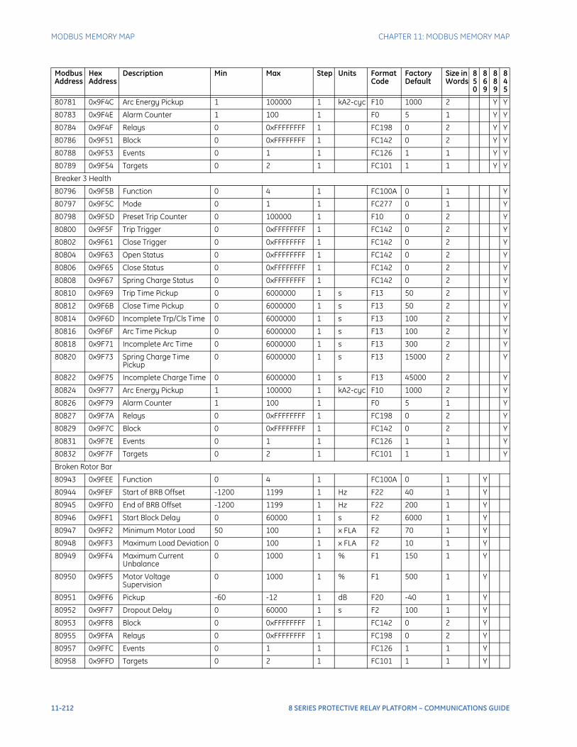
MODBUS MEMORY MAP CHAPTER 11: MODBUS MEMORY MAP
80781 0x9F4C Arc Energy Pickup 1 100000 1 kA2-cyc F10 1000 2 Y Y
80783 0x9F4E Alarm Counter 1 100 1 F0 5 1 Y Y
80784 0x9F4F Relays 0 0xFFFFFFFF 1 FC198 0 2 Y Y
80786 0x9F51 Block 0 0xFFFFFFFF 1 FC142 0 2 Y Y
80788 0x9F53 Events 0 1 1 FC126 1 1 Y Y
80789 0x9F54 Targets 0 2 1 FC101 1 1 Y Y
Breaker 3 Health
80796 0x9F5B Function 0 4 1 FC100A 0 1 Y
80797 0x9F5C Mode 0 1 1 FC277 0 1 Y
80798 0x9F5D Preset Trip Counter 0 100000 1 F10 0 2 Y
80800 0x9F5F Trip Trigger 0 0xFFFFFFFF 1 FC142 0 2 Y
80802 0x9F61 Close Trigger 0 0xFFFFFFFF 1 FC142 0 2 Y
80804 0x9F63 Open Status 0 0xFFFFFFFF 1 FC142 0 2 Y
80806 0x9F65 Close Status 0 0xFFFFFFFF 1 FC142 0 2 Y
80808 0x9F67 Spring Charge Status 0 0xFFFFFFFF 1 FC142 0 2 Y
80810 0x9F69 Trip Time Pickup 0 6000000 1 s F13 50 2 Y
80812 0x9F6B Close Time Pickup 0 6000000 1 s F13 50 2 Y
80814 0x9F6D Incomplete Trp/Cls Time 0 6000000 1 s F13 100 2 Y
80816 0x9F6F Arc Time Pickup 0 6000000 1 s F13 100 2 Y
80818 0x9F71 Incomplete Arc Time 0 6000000 1 s F13 300 2 Y
80820 0x9F73 Spring Charge Time Pickup
0 6000000 1 s F13 15000 2 Y
80822 0x9F75 Incomplete Charge Time 0 6000000 1 s F13 45000 2 Y
80824 0x9F77 Arc Energy Pickup 1 100000 1 kA2-cyc F10 1000 2 Y
80826 0x9F79 Alarm Counter 1 100 1 F0 5 1 Y
80827 0x9F7A Relays 0 0xFFFFFFFF 1 FC198 0 2 Y
80829 0x9F7C Block 0 0xFFFFFFFF 1 FC142 0 2 Y
80831 0x9F7E Events 0 1 1 FC126 1 1 Y
80832 0x9F7F Targets 0 2 1 FC101 1 1 Y
Broken Rotor Bar
80943 0x9FEE Function 0 4 1 FC100A 0 1 Y
80944 0x9FEF Start of BRB Offset -1200 1199 1 Hz F22 40 1 Y
80945 0x9FF0 End of BRB Offset -1200 1199 1 Hz F22 200 1 Y
80946 0x9FF1 Start Block Delay 0 60000 1 s F2 6000 1 Y
80947 0x9FF2 Minimum Motor Load 50 100 1 x FLA F2 70 1 Y
80948 0x9FF3 Maximum Load Deviation 0 100 1 x FLA F2 10 1 Y
80949 0x9FF4 Maximum Current Unbalance
0 1000 1 % F1 150 1 Y
80950 0x9FF5 Motor Voltage Supervision
0 1000 1 % F1 500 1 Y
80951 0x9FF6 Pickup -60 -12 1 dB F20 -40 1 Y
80952 0x9FF7 Dropout Delay 0 60000 1 s F2 100 1 Y
80953 0x9FF8 Block 0 0xFFFFFFFF 1 FC142 0 2 Y
80955 0x9FFA Relays 0 0xFFFFFFFF 1 FC198 0 2 Y
80957 0x9FFC Events 0 1 1 FC126 1 1 Y
80958 0x9FFD Targets 0 2 1 FC101 1 1 Y
Modbus Address
Hex Address
Description Min Max Step Units Format Code
Factory Default
Size in Words
850
869
889
845
11-212 8 SERIES PROTECTIVE RELAY PLATFORM – COMMUNICATIONS GUIDE
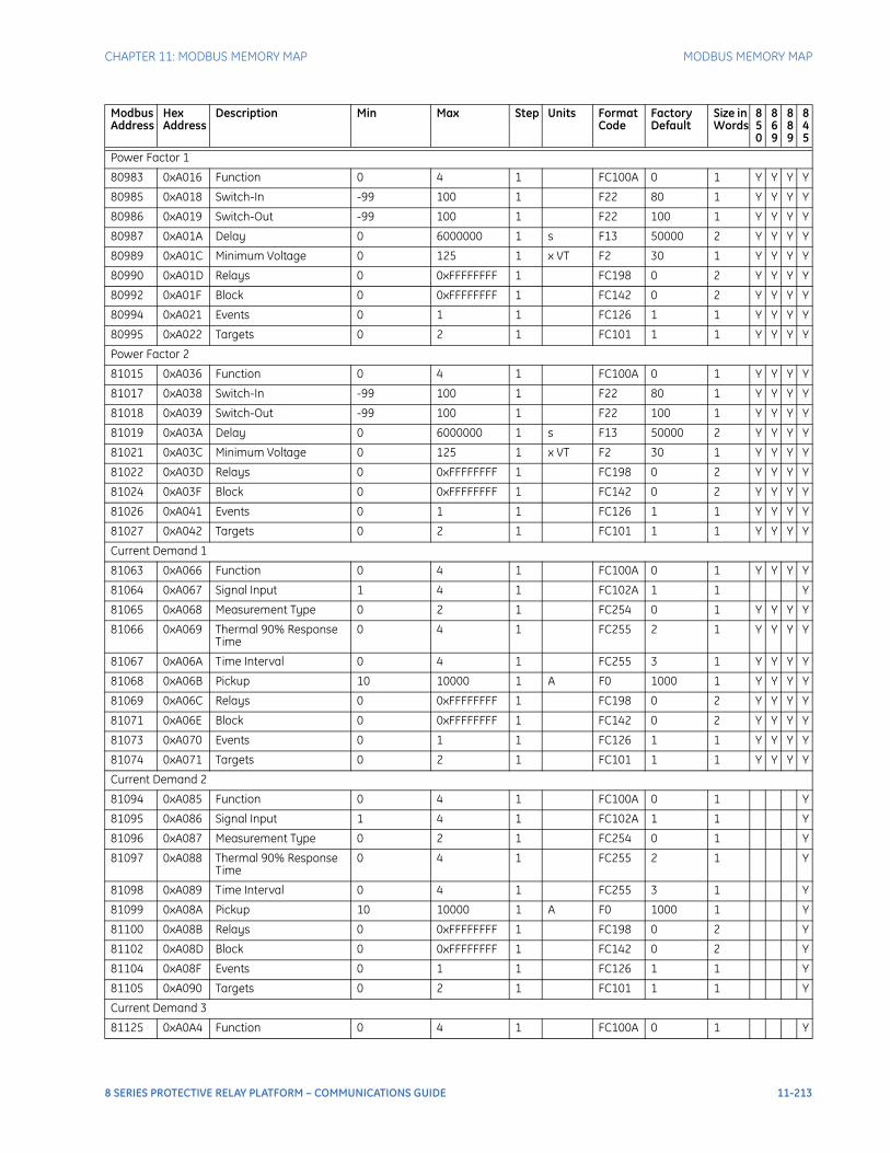
CHAPTER 11: MODBUS MEMORY MAP MODBUS MEMORY MAP
Power Factor 1
80983 0xA016 Function 0 4 1 FC100A 0 1 Y Y Y Y
80985 0xA018 Switch-In -99 100 1 F22 80 1 Y Y Y Y
80986 0xA019 Switch-Out -99 100 1 F22 100 1 Y Y Y Y
80987 0xA01A Delay 0 6000000 1 s F13 50000 2 Y Y Y Y
80989 0xA01C Minimum Voltage 0 125 1 x VT F2 30 1 Y Y Y Y
80990 0xA01D Relays 0 0xFFFFFFFF 1 FC198 0 2 Y Y Y Y
80992 0xA01F Block 0 0xFFFFFFFF 1 FC142 0 2 Y Y Y Y
80994 0xA021 Events 0 1 1 FC126 1 1 Y Y Y Y
80995 0xA022 Targets 0 2 1 FC101 1 1 Y Y Y Y
Power Factor 2
81015 0xA036 Function 0 4 1 FC100A 0 1 Y Y Y Y
81017 0xA038 Switch-In -99 100 1 F22 80 1 Y Y Y Y
81018 0xA039 Switch-Out -99 100 1 F22 100 1 Y Y Y Y
81019 0xA03A Delay 0 6000000 1 s F13 50000 2 Y Y Y Y
81021 0xA03C Minimum Voltage 0 125 1 x VT F2 30 1 Y Y Y Y
81022 0xA03D Relays 0 0xFFFFFFFF 1 FC198 0 2 Y Y Y Y
81024 0xA03F Block 0 0xFFFFFFFF 1 FC142 0 2 Y Y Y Y
81026 0xA041 Events 0 1 1 FC126 1 1 Y Y Y Y
81027 0xA042 Targets 0 2 1 FC101 1 1 Y Y Y Y
Current Demand 1
81063 0xA066 Function 0 4 1 FC100A 0 1 Y Y Y Y
81064 0xA067 Signal Input 1 4 1 FC102A 1 1 Y
81065 0xA068 Measurement Type 0 2 1 FC254 0 1 Y Y Y Y
81066 0xA069 Thermal 90% Response Time
0 4 1 FC255 2 1 Y Y Y Y
81067 0xA06A Time Interval 0 4 1 FC255 3 1 Y Y Y Y
81068 0xA06B Pickup 10 10000 1 A F0 1000 1 Y Y Y Y
81069 0xA06C Relays 0 0xFFFFFFFF 1 FC198 0 2 Y Y Y Y
81071 0xA06E Block 0 0xFFFFFFFF 1 FC142 0 2 Y Y Y Y
81073 0xA070 Events 0 1 1 FC126 1 1 Y Y Y Y
81074 0xA071 Targets 0 2 1 FC101 1 1 Y Y Y Y
Current Demand 2
81094 0xA085 Function 0 4 1 FC100A 0 1 Y
81095 0xA086 Signal Input 1 4 1 FC102A 1 1 Y
81096 0xA087 Measurement Type 0 2 1 FC254 0 1 Y
81097 0xA088 Thermal 90% Response Time
0 4 1 FC255 2 1 Y
81098 0xA089 Time Interval 0 4 1 FC255 3 1 Y
81099 0xA08A Pickup 10 10000 1 A F0 1000 1 Y
81100 0xA08B Relays 0 0xFFFFFFFF 1 FC198 0 2 Y
81102 0xA08D Block 0 0xFFFFFFFF 1 FC142 0 2 Y
81104 0xA08F Events 0 1 1 FC126 1 1 Y
81105 0xA090 Targets 0 2 1 FC101 1 1 Y
Current Demand 3
81125 0xA0A4 Function 0 4 1 FC100A 0 1 Y
Modbus Address
Hex Address
Description Min Max Step Units Format Code
Factory Default
Size in Words
850
869
889
845
8 SERIES PROTECTIVE RELAY PLATFORM – COMMUNICATIONS GUIDE 11-213
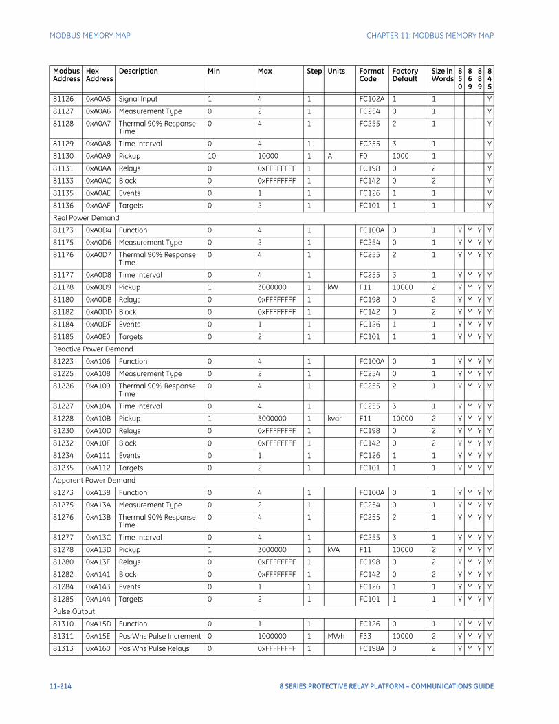
MODBUS MEMORY MAP CHAPTER 11: MODBUS MEMORY MAP
81126 0xA0A5 Signal Input 1 4 1 FC102A 1 1 Y
81127 0xA0A6 Measurement Type 0 2 1 FC254 0 1 Y
81128 0xA0A7 Thermal 90% Response Time
0 4 1 FC255 2 1 Y
81129 0xA0A8 Time Interval 0 4 1 FC255 3 1 Y
81130 0xA0A9 Pickup 10 10000 1 A F0 1000 1 Y
81131 0xA0AA Relays 0 0xFFFFFFFF 1 FC198 0 2 Y
81133 0xA0AC Block 0 0xFFFFFFFF 1 FC142 0 2 Y
81135 0xA0AE Events 0 1 1 FC126 1 1 Y
81136 0xA0AF Targets 0 2 1 FC101 1 1 Y
Real Power Demand
81173 0xA0D4 Function 0 4 1 FC100A 0 1 Y Y Y Y
81175 0xA0D6 Measurement Type 0 2 1 FC254 0 1 Y Y Y Y
81176 0xA0D7 Thermal 90% Response Time
0 4 1 FC255 2 1 Y Y Y Y
81177 0xA0D8 Time Interval 0 4 1 FC255 3 1 Y Y Y Y
81178 0xA0D9 Pickup 1 3000000 1 kW F11 10000 2 Y Y Y Y
81180 0xA0DB Relays 0 0xFFFFFFFF 1 FC198 0 2 Y Y Y Y
81182 0xA0DD Block 0 0xFFFFFFFF 1 FC142 0 2 Y Y Y Y
81184 0xA0DF Events 0 1 1 FC126 1 1 Y Y Y Y
81185 0xA0E0 Targets 0 2 1 FC101 1 1 Y Y Y Y
Reactive Power Demand
81223 0xA106 Function 0 4 1 FC100A 0 1 Y Y Y Y
81225 0xA108 Measurement Type 0 2 1 FC254 0 1 Y Y Y Y
81226 0xA109 Thermal 90% Response Time
0 4 1 FC255 2 1 Y Y Y Y
81227 0xA10A Time Interval 0 4 1 FC255 3 1 Y Y Y Y
81228 0xA10B Pickup 1 3000000 1 kvar F11 10000 2 Y Y Y Y
81230 0xA10D Relays 0 0xFFFFFFFF 1 FC198 0 2 Y Y Y Y
81232 0xA10F Block 0 0xFFFFFFFF 1 FC142 0 2 Y Y Y Y
81234 0xA111 Events 0 1 1 FC126 1 1 Y Y Y Y
81235 0xA112 Targets 0 2 1 FC101 1 1 Y Y Y Y
Apparent Power Demand
81273 0xA138 Function 0 4 1 FC100A 0 1 Y Y Y Y
81275 0xA13A Measurement Type 0 2 1 FC254 0 1 Y Y Y Y
81276 0xA13B Thermal 90% Response Time
0 4 1 FC255 2 1 Y Y Y Y
81277 0xA13C Time Interval 0 4 1 FC255 3 1 Y Y Y Y
81278 0xA13D Pickup 1 3000000 1 kVA F11 10000 2 Y Y Y Y
81280 0xA13F Relays 0 0xFFFFFFFF 1 FC198 0 2 Y Y Y Y
81282 0xA141 Block 0 0xFFFFFFFF 1 FC142 0 2 Y Y Y Y
81284 0xA143 Events 0 1 1 FC126 1 1 Y Y Y Y
81285 0xA144 Targets 0 2 1 FC101 1 1 Y Y Y Y
Pulse Output
81310 0xA15D Function 0 1 1 FC126 0 1 Y Y Y Y
81311 0xA15E Pos Whs Pulse Increment 0 1000000 1 MWh F33 10000 2 Y Y Y Y
81313 0xA160 Pos Whs Pulse Relays 0 0xFFFFFFFF 1 FC198A 0 2 Y Y Y Y
Modbus Address
Hex Address
Description Min Max Step Units Format Code
Factory Default
Size in Words
850
869
889
845
11-214 8 SERIES PROTECTIVE RELAY PLATFORM – COMMUNICATIONS GUIDE

CHAPTER 11: MODBUS MEMORY MAP MODBUS MEMORY MAP
81315 0xA162 Neg Whs Pulse Increment 0 1000000 1 MWh F33 10000 2 Y Y Y Y
81317 0xA164 Neg Whs Pulse Relays 0 0xFFFFFFFF 1 FC198A 0 2 Y Y Y Y
81319 0xA166 Pos VARhs Pulse Increment
0 1000000 1 Mvarh F33 10000 2 Y Y Y Y
81321 0xA168 Pos VARhs Pulse Relays 0 0xFFFFFFFF 1 FC198A 0 2 Y Y Y Y
81323 0xA16A Neg VARhs Pulse Increment
0 1000000 1 Mvarh F33 10000 2 Y Y Y Y
81325 0xA16C Neg VARhs Pulse Relays 0 0xFFFFFFFF 1 FC198A 0 2 Y Y Y Y
81327 0xA16E Events 0 1 1 FC126 1 1 Y Y Y Y
81328 0xA16F Targets 0 2 1 FC101 1 1 Y Y Y Y
Digital Counter 1
81360 0xA18F Function 0 1 1 FC126 0 1 Y Y Y Y
81361 0xA190 Name 0 65535 1 F60_26 Counter 1 13 Y Y Y Y
81374 0xA19D Units 0 65535 1 F60_6 units 3 Y Y Y Y
81377 0xA1A0 Pre-set -2147483648 2147483647 1 F30 0 2 Y Y Y Y
81379 0xA1A2 Compare -2147483648 2147483647 1 F30 0 2 Y Y Y Y
81381 0xA1A4 Up 0 0xFFFFFFFF 1 FC142 0 2 Y Y Y Y
81383 0xA1A6 Down 0 0xFFFFFFFF 1 FC142 0 2 Y Y Y Y
81385 0xA1A8 Set to Pre-set 0 0xFFFFFFFF 1 FC142 0 2 Y Y Y Y
81387 0xA1AA Reset 0 0xFFFFFFFF 1 FC142 0 2 Y Y Y Y
81389 0xA1AC Freeze/Reset 0 0xFFFFFFFF 1 FC142 0 2 Y Y Y Y
81391 0xA1AE Freeze/Count 0 0xFFFFFFFF 1 FC142 0 2 Y Y Y Y
81393 0xA1B0 Block 0 0xFFFFFFFF 1 FC142 0 2 Y Y Y Y
81395 0xA1B2 HI 1 Output Relays 0 0xFFFFFFFF 1 FC198 0 2 Y Y Y Y
81397 0xA1B4 EQL 1 Output Relays 0 0xFFFFFFFF 1 FC198 0 2 Y Y Y Y
81399 0xA1B6 LO 1 Output Relays 0 0xFFFFFFFF 1 FC198 0 2 Y Y Y Y
81401 0xA1B8 Events 0 1 1 FC126 1 1 Y Y Y Y
Digital Counter 2
81402 0xA1B9 Function 0 1 1 FC126 0 1 Y Y Y Y
81403 0xA1BA Name 0 65535 1 F60_26 Counter 2 13 Y Y Y Y
81416 0xA1C7 Units 0 65535 1 F60_6 units 3 Y Y Y Y
81419 0xA1CA Pre-set -2147483648 2147483647 1 F30 0 2 Y Y Y Y
81421 0xA1CC Compare -2147483648 2147483647 1 F30 0 2 Y Y Y Y
81423 0xA1CE Up 0 0xFFFFFFFF 1 FC142 0 2 Y Y Y Y
81425 0xA1D0 Down 0 0xFFFFFFFF 1 FC142 0 2 Y Y Y Y
81427 0xA1D2 Set to Pre-set 0 0xFFFFFFFF 1 FC142 0 2 Y Y Y Y
81429 0xA1D4 Reset 0 0xFFFFFFFF 1 FC142 0 2 Y Y Y Y
81431 0xA1D6 Freeze/Reset 0 0xFFFFFFFF 1 FC142 0 2 Y Y Y Y
81433 0xA1D8 Freeze/Count 0 0xFFFFFFFF 1 FC142 0 2 Y Y Y Y
81435 0xA1DA Block 0 0xFFFFFFFF 1 FC142 0 2 Y Y Y Y
81437 0xA1DC HI 2 Output Relays 0 0xFFFFFFFF 1 FC198 0 2 Y Y Y Y
81439 0xA1DE EQL 2 Output Relays 0 0xFFFFFFFF 1 FC198 0 2 Y Y Y Y
81441 0xA1E0 LO 2 Output Relays 0 0xFFFFFFFF 1 FC198 0 2 Y Y Y Y
81443 0xA1E2 Events 0 1 1 FC126 1 1 Y Y Y Y
Digital Counter 3
81444 0xA1E3 Function 0 1 1 FC126 0 1 Y Y Y Y
Modbus Address
Hex Address
Description Min Max Step Units Format Code
Factory Default
Size in Words
850
869
889
845
8 SERIES PROTECTIVE RELAY PLATFORM – COMMUNICATIONS GUIDE 11-215
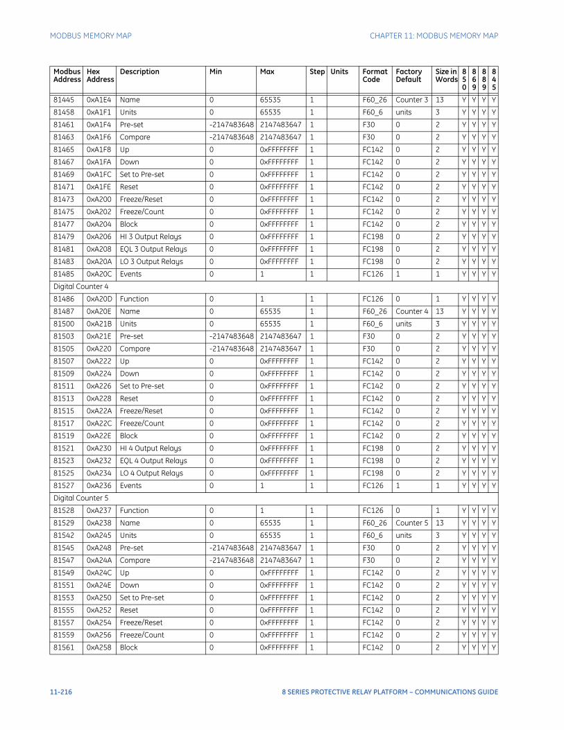
MODBUS MEMORY MAP CHAPTER 11: MODBUS MEMORY MAP
81445 0xA1E4 Name 0 65535 1 F60_26 Counter 3 13 Y Y Y Y
81458 0xA1F1 Units 0 65535 1 F60_6 units 3 Y Y Y Y
81461 0xA1F4 Pre-set -2147483648 2147483647 1 F30 0 2 Y Y Y Y
81463 0xA1F6 Compare -2147483648 2147483647 1 F30 0 2 Y Y Y Y
81465 0xA1F8 Up 0 0xFFFFFFFF 1 FC142 0 2 Y Y Y Y
81467 0xA1FA Down 0 0xFFFFFFFF 1 FC142 0 2 Y Y Y Y
81469 0xA1FC Set to Pre-set 0 0xFFFFFFFF 1 FC142 0 2 Y Y Y Y
81471 0xA1FE Reset 0 0xFFFFFFFF 1 FC142 0 2 Y Y Y Y
81473 0xA200 Freeze/Reset 0 0xFFFFFFFF 1 FC142 0 2 Y Y Y Y
81475 0xA202 Freeze/Count 0 0xFFFFFFFF 1 FC142 0 2 Y Y Y Y
81477 0xA204 Block 0 0xFFFFFFFF 1 FC142 0 2 Y Y Y Y
81479 0xA206 HI 3 Output Relays 0 0xFFFFFFFF 1 FC198 0 2 Y Y Y Y
81481 0xA208 EQL 3 Output Relays 0 0xFFFFFFFF 1 FC198 0 2 Y Y Y Y
81483 0xA20A LO 3 Output Relays 0 0xFFFFFFFF 1 FC198 0 2 Y Y Y Y
81485 0xA20C Events 0 1 1 FC126 1 1 Y Y Y Y
Digital Counter 4
81486 0xA20D Function 0 1 1 FC126 0 1 Y Y Y Y
81487 0xA20E Name 0 65535 1 F60_26 Counter 4 13 Y Y Y Y
81500 0xA21B Units 0 65535 1 F60_6 units 3 Y Y Y Y
81503 0xA21E Pre-set -2147483648 2147483647 1 F30 0 2 Y Y Y Y
81505 0xA220 Compare -2147483648 2147483647 1 F30 0 2 Y Y Y Y
81507 0xA222 Up 0 0xFFFFFFFF 1 FC142 0 2 Y Y Y Y
81509 0xA224 Down 0 0xFFFFFFFF 1 FC142 0 2 Y Y Y Y
81511 0xA226 Set to Pre-set 0 0xFFFFFFFF 1 FC142 0 2 Y Y Y Y
81513 0xA228 Reset 0 0xFFFFFFFF 1 FC142 0 2 Y Y Y Y
81515 0xA22A Freeze/Reset 0 0xFFFFFFFF 1 FC142 0 2 Y Y Y Y
81517 0xA22C Freeze/Count 0 0xFFFFFFFF 1 FC142 0 2 Y Y Y Y
81519 0xA22E Block 0 0xFFFFFFFF 1 FC142 0 2 Y Y Y Y
81521 0xA230 HI 4 Output Relays 0 0xFFFFFFFF 1 FC198 0 2 Y Y Y Y
81523 0xA232 EQL 4 Output Relays 0 0xFFFFFFFF 1 FC198 0 2 Y Y Y Y
81525 0xA234 LO 4 Output Relays 0 0xFFFFFFFF 1 FC198 0 2 Y Y Y Y
81527 0xA236 Events 0 1 1 FC126 1 1 Y Y Y Y
Digital Counter 5
81528 0xA237 Function 0 1 1 FC126 0 1 Y Y Y Y
81529 0xA238 Name 0 65535 1 F60_26 Counter 5 13 Y Y Y Y
81542 0xA245 Units 0 65535 1 F60_6 units 3 Y Y Y Y
81545 0xA248 Pre-set -2147483648 2147483647 1 F30 0 2 Y Y Y Y
81547 0xA24A Compare -2147483648 2147483647 1 F30 0 2 Y Y Y Y
81549 0xA24C Up 0 0xFFFFFFFF 1 FC142 0 2 Y Y Y Y
81551 0xA24E Down 0 0xFFFFFFFF 1 FC142 0 2 Y Y Y Y
81553 0xA250 Set to Pre-set 0 0xFFFFFFFF 1 FC142 0 2 Y Y Y Y
81555 0xA252 Reset 0 0xFFFFFFFF 1 FC142 0 2 Y Y Y Y
81557 0xA254 Freeze/Reset 0 0xFFFFFFFF 1 FC142 0 2 Y Y Y Y
81559 0xA256 Freeze/Count 0 0xFFFFFFFF 1 FC142 0 2 Y Y Y Y
81561 0xA258 Block 0 0xFFFFFFFF 1 FC142 0 2 Y Y Y Y
Modbus Address
Hex Address
Description Min Max Step Units Format Code
Factory Default
Size in Words
850
869
889
845
11-216 8 SERIES PROTECTIVE RELAY PLATFORM – COMMUNICATIONS GUIDE
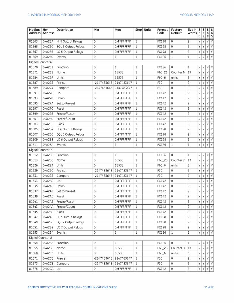
CHAPTER 11: MODBUS MEMORY MAP MODBUS MEMORY MAP
81563 0xA25A HI 5 Output Relays 0 0xFFFFFFFF 1 FC198 0 2 Y Y Y Y
81565 0xA25C EQL 5 Output Relays 0 0xFFFFFFFF 1 FC198 0 2 Y Y Y Y
81567 0xA25E LO 5 Output Relays 0 0xFFFFFFFF 1 FC198 0 2 Y Y Y Y
81569 0xA260 Events 0 1 1 FC126 1 1 Y Y Y Y
Digital Counter 6
81570 0xA261 Function 0 1 1 FC126 0 1 Y Y Y Y
81571 0xA262 Name 0 65535 1 F60_26 Counter 6 13 Y Y Y Y
81584 0xA26F Units 0 65535 1 F60_6 units 3 Y Y Y Y
81587 0xA272 Pre-set -2147483648 2147483647 1 F30 0 2 Y Y Y Y
81589 0xA274 Compare -2147483648 2147483647 1 F30 0 2 Y Y Y Y
81591 0xA276 Up 0 0xFFFFFFFF 1 FC142 0 2 Y Y Y Y
81593 0xA278 Down 0 0xFFFFFFFF 1 FC142 0 2 Y Y Y Y
81595 0xA27A Set to Pre-set 0 0xFFFFFFFF 1 FC142 0 2 Y Y Y Y
81597 0xA27C Reset 0 0xFFFFFFFF 1 FC142 0 2 Y Y Y Y
81599 0xA27E Freeze/Reset 0 0xFFFFFFFF 1 FC142 0 2 Y Y Y Y
81601 0xA280 Freeze/Count 0 0xFFFFFFFF 1 FC142 0 2 Y Y Y Y
81603 0xA282 Block 0 0xFFFFFFFF 1 FC142 0 2 Y Y Y Y
81605 0xA284 HI 6 Output Relays 0 0xFFFFFFFF 1 FC198 0 2 Y Y Y Y
81607 0xA286 EQL 6 Output Relays 0 0xFFFFFFFF 1 FC198 0 2 Y Y Y Y
81609 0xA288 LO 6 Output Relays 0 0xFFFFFFFF 1 FC198 0 2 Y Y Y Y
81611 0xA28A Events 0 1 1 FC126 1 1 Y Y Y Y
Digital Counter 7
81612 0xA28B Function 0 1 1 FC126 0 1 Y Y Y Y
81613 0xA28C Name 0 65535 1 F60_26 Counter 7 13 Y Y Y Y
81626 0xA299 Units 0 65535 1 F60_6 units 3 Y Y Y Y
81629 0xA29C Pre-set -2147483648 2147483647 1 F30 0 2 Y Y Y Y
81631 0xA29E Compare -2147483648 2147483647 1 F30 0 2 Y Y Y Y
81633 0xA2A0 Up 0 0xFFFFFFFF 1 FC142 0 2 Y Y Y Y
81635 0xA2A2 Down 0 0xFFFFFFFF 1 FC142 0 2 Y Y Y Y
81637 0xA2A4 Set to Pre-set 0 0xFFFFFFFF 1 FC142 0 2 Y Y Y Y
81639 0xA2A6 Reset 0 0xFFFFFFFF 1 FC142 0 2 Y Y Y Y
81641 0xA2A8 Freeze/Reset 0 0xFFFFFFFF 1 FC142 0 2 Y Y Y Y
81643 0xA2AA Freeze/Count 0 0xFFFFFFFF 1 FC142 0 2 Y Y Y Y
81645 0xA2AC Block 0 0xFFFFFFFF 1 FC142 0 2 Y Y Y Y
81647 0xA2AE HI 7 Output Relays 0 0xFFFFFFFF 1 FC198 0 2 Y Y Y Y
81649 0xA2B0 EQL 7 Output Relays 0 0xFFFFFFFF 1 FC198 0 2 Y Y Y Y
81651 0xA2B2 LO 7 Output Relays 0 0xFFFFFFFF 1 FC198 0 2 Y Y Y Y
81653 0xA2B4 Events 0 1 1 FC126 1 1 Y Y Y Y
Digital Counter 8
81654 0xA2B5 Function 0 1 1 FC126 0 1 Y Y Y Y
81655 0xA2B6 Name 0 65535 1 F60_26 Counter 8 13 Y Y Y Y
81668 0xA2C3 Units 0 65535 1 F60_6 units 3 Y Y Y Y
81671 0xA2C6 Pre-set -2147483648 2147483647 1 F30 0 2 Y Y Y Y
81673 0xA2C8 Compare -2147483648 2147483647 1 F30 0 2 Y Y Y Y
81675 0xA2CA Up 0 0xFFFFFFFF 1 FC142 0 2 Y Y Y Y
Modbus Address
Hex Address
Description Min Max Step Units Format Code
Factory Default
Size in Words
850
869
889
845
8 SERIES PROTECTIVE RELAY PLATFORM – COMMUNICATIONS GUIDE 11-217
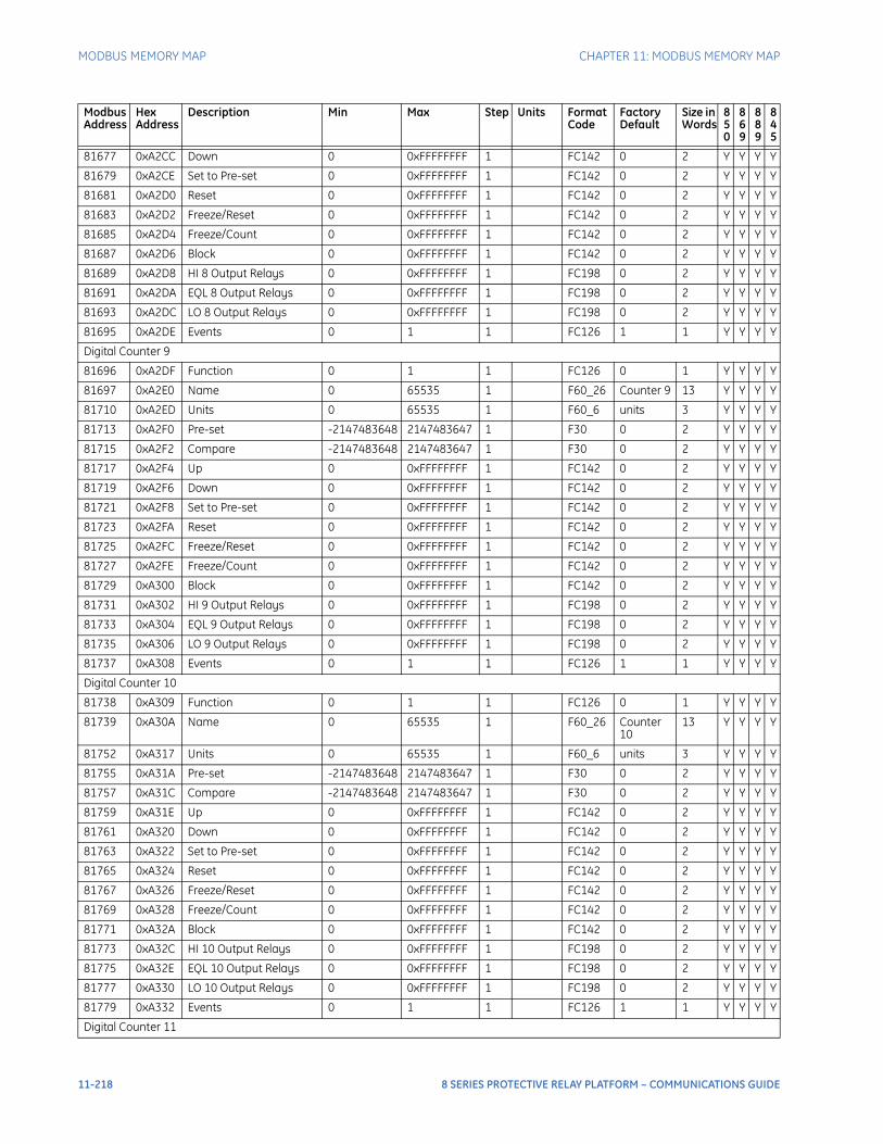
MODBUS MEMORY MAP CHAPTER 11: MODBUS MEMORY MAP
81677 0xA2CC Down 0 0xFFFFFFFF 1 FC142 0 2 Y Y Y Y
81679 0xA2CE Set to Pre-set 0 0xFFFFFFFF 1 FC142 0 2 Y Y Y Y
81681 0xA2D0 Reset 0 0xFFFFFFFF 1 FC142 0 2 Y Y Y Y
81683 0xA2D2 Freeze/Reset 0 0xFFFFFFFF 1 FC142 0 2 Y Y Y Y
81685 0xA2D4 Freeze/Count 0 0xFFFFFFFF 1 FC142 0 2 Y Y Y Y
81687 0xA2D6 Block 0 0xFFFFFFFF 1 FC142 0 2 Y Y Y Y
81689 0xA2D8 HI 8 Output Relays 0 0xFFFFFFFF 1 FC198 0 2 Y Y Y Y
81691 0xA2DA EQL 8 Output Relays 0 0xFFFFFFFF 1 FC198 0 2 Y Y Y Y
81693 0xA2DC LO 8 Output Relays 0 0xFFFFFFFF 1 FC198 0 2 Y Y Y Y
81695 0xA2DE Events 0 1 1 FC126 1 1 Y Y Y Y
Digital Counter 9
81696 0xA2DF Function 0 1 1 FC126 0 1 Y Y Y Y
81697 0xA2E0 Name 0 65535 1 F60_26 Counter 9 13 Y Y Y Y
81710 0xA2ED Units 0 65535 1 F60_6 units 3 Y Y Y Y
81713 0xA2F0 Pre-set -2147483648 2147483647 1 F30 0 2 Y Y Y Y
81715 0xA2F2 Compare -2147483648 2147483647 1 F30 0 2 Y Y Y Y
81717 0xA2F4 Up 0 0xFFFFFFFF 1 FC142 0 2 Y Y Y Y
81719 0xA2F6 Down 0 0xFFFFFFFF 1 FC142 0 2 Y Y Y Y
81721 0xA2F8 Set to Pre-set 0 0xFFFFFFFF 1 FC142 0 2 Y Y Y Y
81723 0xA2FA Reset 0 0xFFFFFFFF 1 FC142 0 2 Y Y Y Y
81725 0xA2FC Freeze/Reset 0 0xFFFFFFFF 1 FC142 0 2 Y Y Y Y
81727 0xA2FE Freeze/Count 0 0xFFFFFFFF 1 FC142 0 2 Y Y Y Y
81729 0xA300 Block 0 0xFFFFFFFF 1 FC142 0 2 Y Y Y Y
81731 0xA302 HI 9 Output Relays 0 0xFFFFFFFF 1 FC198 0 2 Y Y Y Y
81733 0xA304 EQL 9 Output Relays 0 0xFFFFFFFF 1 FC198 0 2 Y Y Y Y
81735 0xA306 LO 9 Output Relays 0 0xFFFFFFFF 1 FC198 0 2 Y Y Y Y
81737 0xA308 Events 0 1 1 FC126 1 1 Y Y Y Y
Digital Counter 10
81738 0xA309 Function 0 1 1 FC126 0 1 Y Y Y Y
81739 0xA30A Name 0 65535 1 F60_26 Counter 10
13 Y Y Y Y
81752 0xA317 Units 0 65535 1 F60_6 units 3 Y Y Y Y
81755 0xA31A Pre-set -2147483648 2147483647 1 F30 0 2 Y Y Y Y
81757 0xA31C Compare -2147483648 2147483647 1 F30 0 2 Y Y Y Y
81759 0xA31E Up 0 0xFFFFFFFF 1 FC142 0 2 Y Y Y Y
81761 0xA320 Down 0 0xFFFFFFFF 1 FC142 0 2 Y Y Y Y
81763 0xA322 Set to Pre-set 0 0xFFFFFFFF 1 FC142 0 2 Y Y Y Y
81765 0xA324 Reset 0 0xFFFFFFFF 1 FC142 0 2 Y Y Y Y
81767 0xA326 Freeze/Reset 0 0xFFFFFFFF 1 FC142 0 2 Y Y Y Y
81769 0xA328 Freeze/Count 0 0xFFFFFFFF 1 FC142 0 2 Y Y Y Y
81771 0xA32A Block 0 0xFFFFFFFF 1 FC142 0 2 Y Y Y Y
81773 0xA32C HI 10 Output Relays 0 0xFFFFFFFF 1 FC198 0 2 Y Y Y Y
81775 0xA32E EQL 10 Output Relays 0 0xFFFFFFFF 1 FC198 0 2 Y Y Y Y
81777 0xA330 LO 10 Output Relays 0 0xFFFFFFFF 1 FC198 0 2 Y Y Y Y
81779 0xA332 Events 0 1 1 FC126 1 1 Y Y Y Y
Digital Counter 11
Modbus Address
Hex Address
Description Min Max Step Units Format Code
Factory Default
Size in Words
850
869
889
845
11-218 8 SERIES PROTECTIVE RELAY PLATFORM – COMMUNICATIONS GUIDE
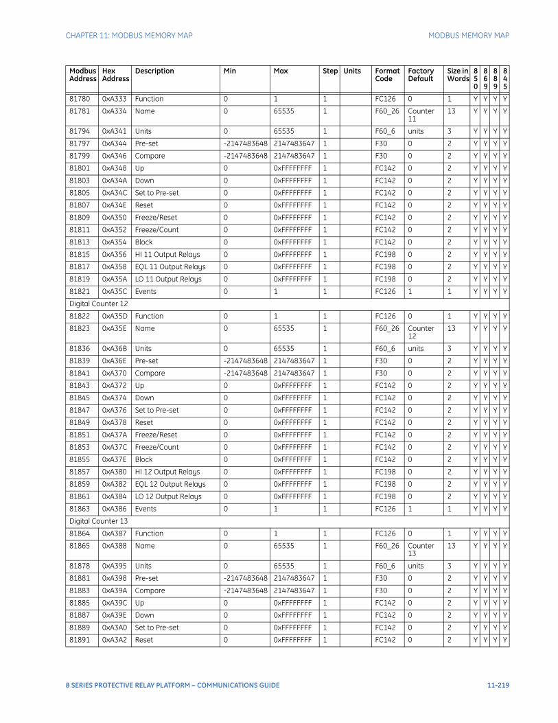
CHAPTER 11: MODBUS MEMORY MAP MODBUS MEMORY MAP
81780 0xA333 Function 0 1 1 FC126 0 1 Y Y Y Y
81781 0xA334 Name 0 65535 1 F60_26 Counter 11
13 Y Y Y Y
81794 0xA341 Units 0 65535 1 F60_6 units 3 Y Y Y Y
81797 0xA344 Pre-set -2147483648 2147483647 1 F30 0 2 Y Y Y Y
81799 0xA346 Compare -2147483648 2147483647 1 F30 0 2 Y Y Y Y
81801 0xA348 Up 0 0xFFFFFFFF 1 FC142 0 2 Y Y Y Y
81803 0xA34A Down 0 0xFFFFFFFF 1 FC142 0 2 Y Y Y Y
81805 0xA34C Set to Pre-set 0 0xFFFFFFFF 1 FC142 0 2 Y Y Y Y
81807 0xA34E Reset 0 0xFFFFFFFF 1 FC142 0 2 Y Y Y Y
81809 0xA350 Freeze/Reset 0 0xFFFFFFFF 1 FC142 0 2 Y Y Y Y
81811 0xA352 Freeze/Count 0 0xFFFFFFFF 1 FC142 0 2 Y Y Y Y
81813 0xA354 Block 0 0xFFFFFFFF 1 FC142 0 2 Y Y Y Y
81815 0xA356 HI 11 Output Relays 0 0xFFFFFFFF 1 FC198 0 2 Y Y Y Y
81817 0xA358 EQL 11 Output Relays 0 0xFFFFFFFF 1 FC198 0 2 Y Y Y Y
81819 0xA35A LO 11 Output Relays 0 0xFFFFFFFF 1 FC198 0 2 Y Y Y Y
81821 0xA35C Events 0 1 1 FC126 1 1 Y Y Y Y
Digital Counter 12
81822 0xA35D Function 0 1 1 FC126 0 1 Y Y Y Y
81823 0xA35E Name 0 65535 1 F60_26 Counter 12
13 Y Y Y Y
81836 0xA36B Units 0 65535 1 F60_6 units 3 Y Y Y Y
81839 0xA36E Pre-set -2147483648 2147483647 1 F30 0 2 Y Y Y Y
81841 0xA370 Compare -2147483648 2147483647 1 F30 0 2 Y Y Y Y
81843 0xA372 Up 0 0xFFFFFFFF 1 FC142 0 2 Y Y Y Y
81845 0xA374 Down 0 0xFFFFFFFF 1 FC142 0 2 Y Y Y Y
81847 0xA376 Set to Pre-set 0 0xFFFFFFFF 1 FC142 0 2 Y Y Y Y
81849 0xA378 Reset 0 0xFFFFFFFF 1 FC142 0 2 Y Y Y Y
81851 0xA37A Freeze/Reset 0 0xFFFFFFFF 1 FC142 0 2 Y Y Y Y
81853 0xA37C Freeze/Count 0 0xFFFFFFFF 1 FC142 0 2 Y Y Y Y
81855 0xA37E Block 0 0xFFFFFFFF 1 FC142 0 2 Y Y Y Y
81857 0xA380 HI 12 Output Relays 0 0xFFFFFFFF 1 FC198 0 2 Y Y Y Y
81859 0xA382 EQL 12 Output Relays 0 0xFFFFFFFF 1 FC198 0 2 Y Y Y Y
81861 0xA384 LO 12 Output Relays 0 0xFFFFFFFF 1 FC198 0 2 Y Y Y Y
81863 0xA386 Events 0 1 1 FC126 1 1 Y Y Y Y
Digital Counter 13
81864 0xA387 Function 0 1 1 FC126 0 1 Y Y Y Y
81865 0xA388 Name 0 65535 1 F60_26 Counter 13
13 Y Y Y Y
81878 0xA395 Units 0 65535 1 F60_6 units 3 Y Y Y Y
81881 0xA398 Pre-set -2147483648 2147483647 1 F30 0 2 Y Y Y Y
81883 0xA39A Compare -2147483648 2147483647 1 F30 0 2 Y Y Y Y
81885 0xA39C Up 0 0xFFFFFFFF 1 FC142 0 2 Y Y Y Y
81887 0xA39E Down 0 0xFFFFFFFF 1 FC142 0 2 Y Y Y Y
81889 0xA3A0 Set to Pre-set 0 0xFFFFFFFF 1 FC142 0 2 Y Y Y Y
81891 0xA3A2 Reset 0 0xFFFFFFFF 1 FC142 0 2 Y Y Y Y
Modbus Address
Hex Address
Description Min Max Step Units Format Code
Factory Default
Size in Words
850
869
889
845
8 SERIES PROTECTIVE RELAY PLATFORM – COMMUNICATIONS GUIDE 11-219
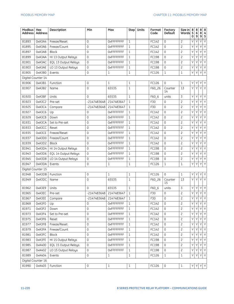
MODBUS MEMORY MAP CHAPTER 11: MODBUS MEMORY MAP
81893 0xA3A4 Freeze/Reset 0 0xFFFFFFFF 1 FC142 0 2 Y Y Y Y
81895 0xA3A6 Freeze/Count 0 0xFFFFFFFF 1 FC142 0 2 Y Y Y Y
81897 0xA3A8 Block 0 0xFFFFFFFF 1 FC142 0 2 Y Y Y Y
81899 0xA3AA HI 13 Output Relays 0 0xFFFFFFFF 1 FC198 0 2 Y Y Y Y
81901 0xA3AC EQL 13 Output Relays 0 0xFFFFFFFF 1 FC198 0 2 Y Y Y Y
81903 0xA3AE LO 13 Output Relays 0 0xFFFFFFFF 1 FC198 0 2 Y Y Y Y
81905 0xA3B0 Events 0 1 1 FC126 1 1 Y Y Y Y
Digital Counter 14
81906 0xA3B1 Function 0 1 1 FC126 0 1 Y Y Y Y
81907 0xA3B2 Name 0 65535 1 F60_26 Counter 14
13 Y Y Y Y
81920 0xA3BF Units 0 65535 1 F60_6 units 3 Y Y Y Y
81923 0xA3C2 Pre-set -2147483648 2147483647 1 F30 0 2 Y Y Y Y
81925 0xA3C4 Compare -2147483648 2147483647 1 F30 0 2 Y Y Y Y
81927 0xA3C6 Up 0 0xFFFFFFFF 1 FC142 0 2 Y Y Y Y
81929 0xA3C8 Down 0 0xFFFFFFFF 1 FC142 0 2 Y Y Y Y
81931 0xA3CA Set to Pre-set 0 0xFFFFFFFF 1 FC142 0 2 Y Y Y Y
81933 0xA3CC Reset 0 0xFFFFFFFF 1 FC142 0 2 Y Y Y Y
81935 0xA3CE Freeze/Reset 0 0xFFFFFFFF 1 FC142 0 2 Y Y Y Y
81937 0xA3D0 Freeze/Count 0 0xFFFFFFFF 1 FC142 0 2 Y Y Y Y
81939 0xA3D2 Block 0 0xFFFFFFFF 1 FC142 0 2 Y Y Y Y
81941 0xA3D4 HI 14 Output Relays 0 0xFFFFFFFF 1 FC198 0 2 Y Y Y Y
81943 0xA3D6 EQL 14 Output Relays 0 0xFFFFFFFF 1 FC198 0 2 Y Y Y Y
81945 0xA3D8 LO 14 Output Relays 0 0xFFFFFFFF 1 FC198 0 2 Y Y Y Y
81947 0xA3DA Events 0 1 1 FC126 1 1 Y Y Y Y
Digital Counter 15
81948 0xA3DB Function 0 1 1 FC126 0 1 Y Y Y Y
81949 0xA3DC Name 0 65535 1 F60_26 Counter 15
13 Y Y Y Y
81962 0xA3E9 Units 0 65535 1 F60_6 units 3 Y Y Y Y
81965 0xA3EC Pre-set -2147483648 2147483647 1 F30 0 2 Y Y Y Y
81967 0xA3EE Compare -2147483648 2147483647 1 F30 0 2 Y Y Y Y
81969 0xA3F0 Up 0 0xFFFFFFFF 1 FC142 0 2 Y Y Y Y
81971 0xA3F2 Down 0 0xFFFFFFFF 1 FC142 0 2 Y Y Y Y
81973 0xA3F4 Set to Pre-set 0 0xFFFFFFFF 1 FC142 0 2 Y Y Y Y
81975 0xA3F6 Reset 0 0xFFFFFFFF 1 FC142 0 2 Y Y Y Y
81977 0xA3F8 Freeze/Reset 0 0xFFFFFFFF 1 FC142 0 2 Y Y Y Y
81979 0xA3FA Freeze/Count 0 0xFFFFFFFF 1 FC142 0 2 Y Y Y Y
81981 0xA3FC Block 0 0xFFFFFFFF 1 FC142 0 2 Y Y Y Y
81983 0xA3FE HI 15 Output Relays 0 0xFFFFFFFF 1 FC198 0 2 Y Y Y Y
81985 0xA400 EQL 15 Output Relays 0 0xFFFFFFFF 1 FC198 0 2 Y Y Y Y
81987 0xA402 LO 15 Output Relays 0 0xFFFFFFFF 1 FC198 0 2 Y Y Y Y
81989 0xA404 Events 0 1 1 FC126 1 1 Y Y Y Y
Digital Counter 16
81990 0xA405 Function 0 1 1 FC126 0 1 Y Y Y Y
Modbus Address
Hex Address
Description Min Max Step Units Format Code
Factory Default
Size in Words
850
869
889
845
11-220 8 SERIES PROTECTIVE RELAY PLATFORM – COMMUNICATIONS GUIDE
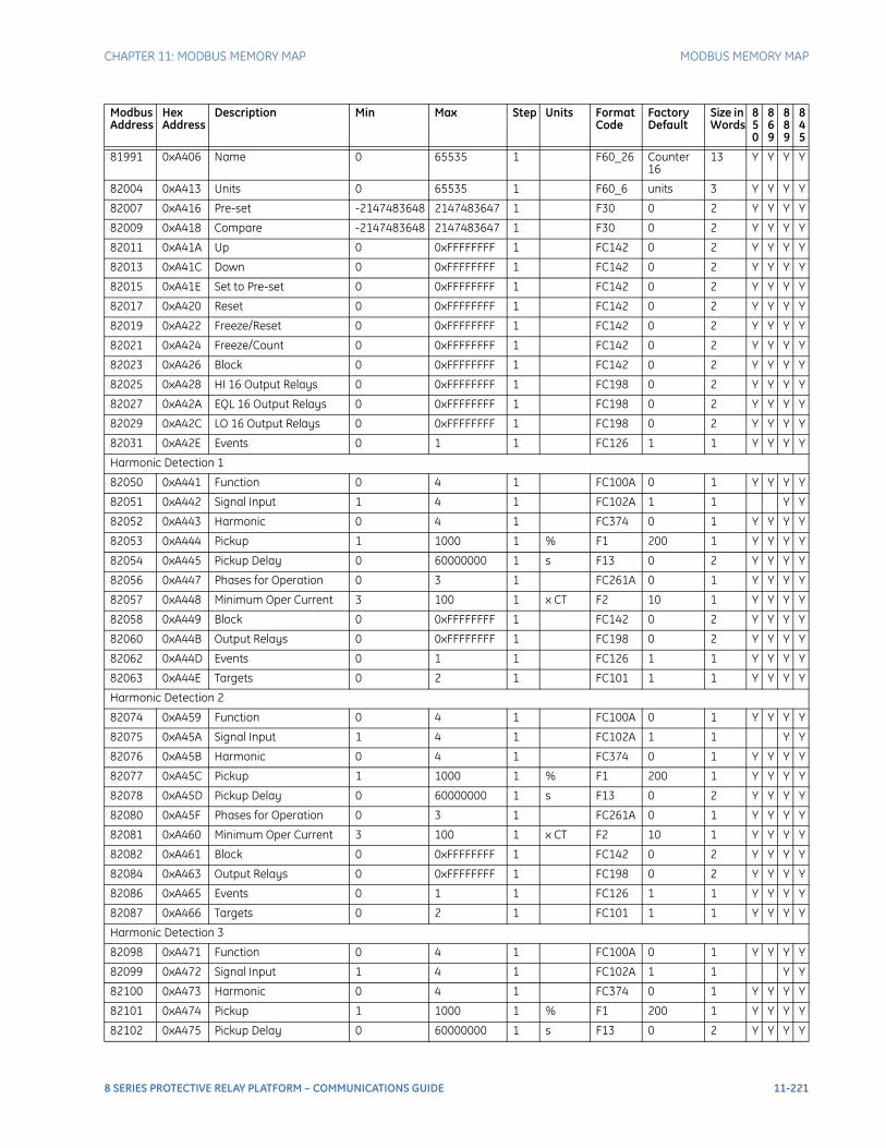
CHAPTER 11: MODBUS MEMORY MAP MODBUS MEMORY MAP
81991 0xA406 Name 0 65535 1 F60_26 Counter 16
13 Y Y Y Y
82004 0xA413 Units 0 65535 1 F60_6 units 3 Y Y Y Y
82007 0xA416 Pre-set -2147483648 2147483647 1 F30 0 2 Y Y Y Y
82009 0xA418 Compare -2147483648 2147483647 1 F30 0 2 Y Y Y Y
82011 0xA41A Up 0 0xFFFFFFFF 1 FC142 0 2 Y Y Y Y
82013 0xA41C Down 0 0xFFFFFFFF 1 FC142 0 2 Y Y Y Y
82015 0xA41E Set to Pre-set 0 0xFFFFFFFF 1 FC142 0 2 Y Y Y Y
82017 0xA420 Reset 0 0xFFFFFFFF 1 FC142 0 2 Y Y Y Y
82019 0xA422 Freeze/Reset 0 0xFFFFFFFF 1 FC142 0 2 Y Y Y Y
82021 0xA424 Freeze/Count 0 0xFFFFFFFF 1 FC142 0 2 Y Y Y Y
82023 0xA426 Block 0 0xFFFFFFFF 1 FC142 0 2 Y Y Y Y
82025 0xA428 HI 16 Output Relays 0 0xFFFFFFFF 1 FC198 0 2 Y Y Y Y
82027 0xA42A EQL 16 Output Relays 0 0xFFFFFFFF 1 FC198 0 2 Y Y Y Y
82029 0xA42C LO 16 Output Relays 0 0xFFFFFFFF 1 FC198 0 2 Y Y Y Y
82031 0xA42E Events 0 1 1 FC126 1 1 Y Y Y Y
Harmonic Detection 1
82050 0xA441 Function 0 4 1 FC100A 0 1 Y Y Y Y
82051 0xA442 Signal Input 1 4 1 FC102A 1 1 Y Y
82052 0xA443 Harmonic 0 4 1 FC374 0 1 Y Y Y Y
82053 0xA444 Pickup 1 1000 1 % F1 200 1 Y Y Y Y
82054 0xA445 Pickup Delay 0 60000000 1 s F13 0 2 Y Y Y Y
82056 0xA447 Phases for Operation 0 3 1 FC261A 0 1 Y Y Y Y
82057 0xA448 Minimum Oper Current 3 100 1 x CT F2 10 1 Y Y Y Y
82058 0xA449 Block 0 0xFFFFFFFF 1 FC142 0 2 Y Y Y Y
82060 0xA44B Output Relays 0 0xFFFFFFFF 1 FC198 0 2 Y Y Y Y
82062 0xA44D Events 0 1 1 FC126 1 1 Y Y Y Y
82063 0xA44E Targets 0 2 1 FC101 1 1 Y Y Y Y
Harmonic Detection 2
82074 0xA459 Function 0 4 1 FC100A 0 1 Y Y Y Y
82075 0xA45A Signal Input 1 4 1 FC102A 1 1 Y Y
82076 0xA45B Harmonic 0 4 1 FC374 0 1 Y Y Y Y
82077 0xA45C Pickup 1 1000 1 % F1 200 1 Y Y Y Y
82078 0xA45D Pickup Delay 0 60000000 1 s F13 0 2 Y Y Y Y
82080 0xA45F Phases for Operation 0 3 1 FC261A 0 1 Y Y Y Y
82081 0xA460 Minimum Oper Current 3 100 1 x CT F2 10 1 Y Y Y Y
82082 0xA461 Block 0 0xFFFFFFFF 1 FC142 0 2 Y Y Y Y
82084 0xA463 Output Relays 0 0xFFFFFFFF 1 FC198 0 2 Y Y Y Y
82086 0xA465 Events 0 1 1 FC126 1 1 Y Y Y Y
82087 0xA466 Targets 0 2 1 FC101 1 1 Y Y Y Y
Harmonic Detection 3
82098 0xA471 Function 0 4 1 FC100A 0 1 Y Y Y Y
82099 0xA472 Signal Input 1 4 1 FC102A 1 1 Y Y
82100 0xA473 Harmonic 0 4 1 FC374 0 1 Y Y Y Y
82101 0xA474 Pickup 1 1000 1 % F1 200 1 Y Y Y Y
82102 0xA475 Pickup Delay 0 60000000 1 s F13 0 2 Y Y Y Y
Modbus Address
Hex Address
Description Min Max Step Units Format Code
Factory Default
Size in Words
850
869
889
845
8 SERIES PROTECTIVE RELAY PLATFORM – COMMUNICATIONS GUIDE 11-221
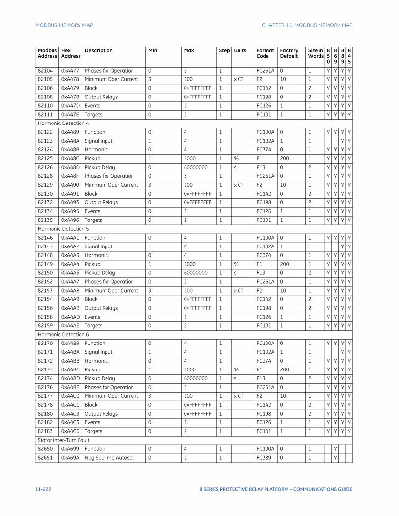
MODBUS MEMORY MAP CHAPTER 11: MODBUS MEMORY MAP
82104 0xA477 Phases for Operation 0 3 1 FC261A 0 1 Y Y Y Y
82105 0xA478 Minimum Oper Current 3 100 1 x CT F2 10 1 Y Y Y Y
82106 0xA479 Block 0 0xFFFFFFFF 1 FC142 0 2 Y Y Y Y
82108 0xA47B Output Relays 0 0xFFFFFFFF 1 FC198 0 2 Y Y Y Y
82110 0xA47D Events 0 1 1 FC126 1 1 Y Y Y Y
82111 0xA47E Targets 0 2 1 FC101 1 1 Y Y Y Y
Harmonic Detection 4
82122 0xA489 Function 0 4 1 FC100A 0 1 Y Y Y Y
82123 0xA48A Signal Input 1 4 1 FC102A 1 1 Y Y
82124 0xA48B Harmonic 0 4 1 FC374 0 1 Y Y Y Y
82125 0xA48C Pickup 1 1000 1 % F1 200 1 Y Y Y Y
82126 0xA48D Pickup Delay 0 60000000 1 s F13 0 2 Y Y Y Y
82128 0xA48F Phases for Operation 0 3 1 FC261A 0 1 Y Y Y Y
82129 0xA490 Minimum Oper Current 3 100 1 x CT F2 10 1 Y Y Y Y
82130 0xA491 Block 0 0xFFFFFFFF 1 FC142 0 2 Y Y Y Y
82132 0xA493 Output Relays 0 0xFFFFFFFF 1 FC198 0 2 Y Y Y Y
82134 0xA495 Events 0 1 1 FC126 1 1 Y Y Y Y
82135 0xA496 Targets 0 2 1 FC101 1 1 Y Y Y Y
Harmonic Detection 5
82146 0xA4A1 Function 0 4 1 FC100A 0 1 Y Y Y Y
82147 0xA4A2 Signal Input 1 4 1 FC102A 1 1 Y Y
82148 0xA4A3 Harmonic 0 4 1 FC374 0 1 Y Y Y Y
82149 0xA4A4 Pickup 1 1000 1 % F1 200 1 Y Y Y Y
82150 0xA4A5 Pickup Delay 0 60000000 1 s F13 0 2 Y Y Y Y
82152 0xA4A7 Phases for Operation 0 3 1 FC261A 0 1 Y Y Y Y
82153 0xA4A8 Minimum Oper Current 3 100 1 x CT F2 10 1 Y Y Y Y
82154 0xA4A9 Block 0 0xFFFFFFFF 1 FC142 0 2 Y Y Y Y
82156 0xA4AB Output Relays 0 0xFFFFFFFF 1 FC198 0 2 Y Y Y Y
82158 0xA4AD Events 0 1 1 FC126 1 1 Y Y Y Y
82159 0xA4AE Targets 0 2 1 FC101 1 1 Y Y Y Y
Harmonic Detection 6
82170 0xA4B9 Function 0 4 1 FC100A 0 1 Y Y Y Y
82171 0xA4BA Signal Input 1 4 1 FC102A 1 1 Y Y
82172 0xA4BB Harmonic 0 4 1 FC374 0 1 Y Y Y Y
82173 0xA4BC Pickup 1 1000 1 % F1 200 1 Y Y Y Y
82174 0xA4BD Pickup Delay 0 60000000 1 s F13 0 2 Y Y Y Y
82176 0xA4BF Phases for Operation 0 3 1 FC261A 0 1 Y Y Y Y
82177 0xA4C0 Minimum Oper Current 3 100 1 x CT F2 10 1 Y Y Y Y
82178 0xA4C1 Block 0 0xFFFFFFFF 1 FC142 0 2 Y Y Y Y
82180 0xA4C3 Output Relays 0 0xFFFFFFFF 1 FC198 0 2 Y Y Y Y
82182 0xA4C5 Events 0 1 1 FC126 1 1 Y Y Y Y
82183 0xA4C6 Targets 0 2 1 FC101 1 1 Y Y Y Y
Stator Inter-Turn Fault
82650 0xA699 Function 0 4 1 FC100A 0 1 Y
82651 0xA69A Neg Seq Imp Autoset 0 1 1 FC389 0 1 Y
Modbus Address
Hex Address
Description Min Max Step Units Format Code
Factory Default
Size in Words
850
869
889
845
11-222 8 SERIES PROTECTIVE RELAY PLATFORM – COMMUNICATIONS GUIDE
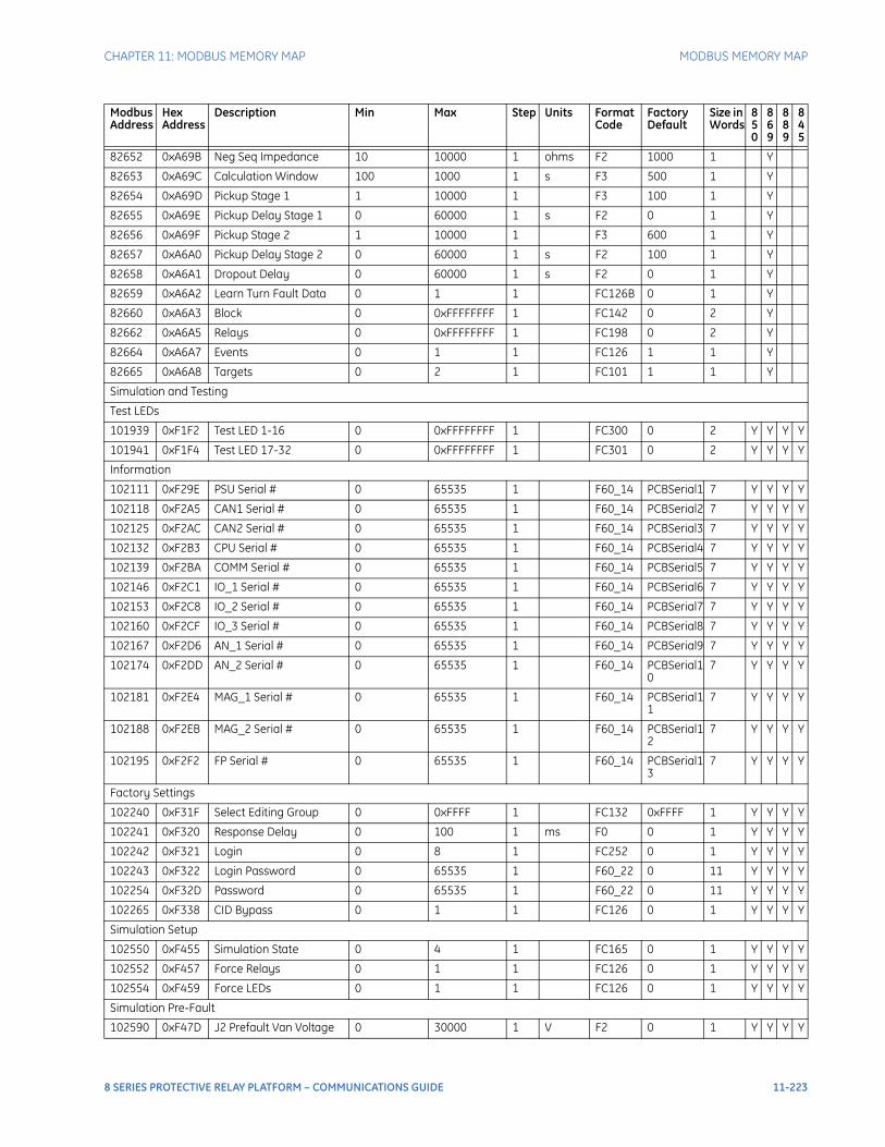
CHAPTER 11: MODBUS MEMORY MAP MODBUS MEMORY MAP
82652 0xA69B Neg Seq Impedance 10 10000 1 ohms F2 1000 1 Y
82653 0xA69C Calculation Window 100 1000 1 s F3 500 1 Y
82654 0xA69D Pickup Stage 1 1 10000 1 F3 100 1 Y
82655 0xA69E Pickup Delay Stage 1 0 60000 1 s F2 0 1 Y
82656 0xA69F Pickup Stage 2 1 10000 1 F3 600 1 Y
82657 0xA6A0 Pickup Delay Stage 2 0 60000 1 s F2 100 1 Y
82658 0xA6A1 Dropout Delay 0 60000 1 s F2 0 1 Y
82659 0xA6A2 Learn Turn Fault Data 0 1 1 FC126B 0 1 Y
82660 0xA6A3 Block 0 0xFFFFFFFF 1 FC142 0 2 Y
82662 0xA6A5 Relays 0 0xFFFFFFFF 1 FC198 0 2 Y
82664 0xA6A7 Events 0 1 1 FC126 1 1 Y
82665 0xA6A8 Targets 0 2 1 FC101 1 1 Y
Simulation and Testing
Test LEDs
101939 0xF1F2 Test LED 1-16 0 0xFFFFFFFF 1 FC300 0 2 Y Y Y Y
101941 0xF1F4 Test LED 17-32 0 0xFFFFFFFF 1 FC301 0 2 Y Y Y Y
Information
102111 0xF29E PSU Serial # 0 65535 1 F60_14 PCBSerial1 7 Y Y Y Y
102118 0xF2A5 CAN1 Serial # 0 65535 1 F60_14 PCBSerial2 7 Y Y Y Y
102125 0xF2AC CAN2 Serial # 0 65535 1 F60_14 PCBSerial3 7 Y Y Y Y
102132 0xF2B3 CPU Serial # 0 65535 1 F60_14 PCBSerial4 7 Y Y Y Y
102139 0xF2BA COMM Serial # 0 65535 1 F60_14 PCBSerial5 7 Y Y Y Y
102146 0xF2C1 IO_1 Serial # 0 65535 1 F60_14 PCBSerial6 7 Y Y Y Y
102153 0xF2C8 IO_2 Serial # 0 65535 1 F60_14 PCBSerial7 7 Y Y Y Y
102160 0xF2CF IO_3 Serial # 0 65535 1 F60_14 PCBSerial8 7 Y Y Y Y
102167 0xF2D6 AN_1 Serial # 0 65535 1 F60_14 PCBSerial9 7 Y Y Y Y
102174 0xF2DD AN_2 Serial # 0 65535 1 F60_14 PCBSerial10
7 Y Y Y Y
102181 0xF2E4 MAG_1 Serial # 0 65535 1 F60_14 PCBSerial11
7 Y Y Y Y
102188 0xF2EB MAG_2 Serial # 0 65535 1 F60_14 PCBSerial12
7 Y Y Y Y
102195 0xF2F2 FP Serial # 0 65535 1 F60_14 PCBSerial13
7 Y Y Y Y
Factory Settings
102240 0xF31F Select Editing Group 0 0xFFFF 1 FC132 0xFFFF 1 Y Y Y Y
102241 0xF320 Response Delay 0 100 1 ms F0 0 1 Y Y Y Y
102242 0xF321 Login 0 8 1 FC252 0 1 Y Y Y Y
102243 0xF322 Login Password 0 65535 1 F60_22 0 11 Y Y Y Y
102254 0xF32D Password 0 65535 1 F60_22 0 11 Y Y Y Y
102265 0xF338 CID Bypass 0 1 1 FC126 0 1 Y Y Y Y
Simulation Setup
102550 0xF455 Simulation State 0 4 1 FC165 0 1 Y Y Y Y
102552 0xF457 Force Relays 0 1 1 FC126 0 1 Y Y Y Y
102554 0xF459 Force LEDs 0 1 1 FC126 0 1 Y Y Y Y
Simulation Pre-Fault
102590 0xF47D J2 Prefault Van Voltage 0 30000 1 V F2 0 1 Y Y Y Y
Modbus Address
Hex Address
Description Min Max Step Units Format Code
Factory Default
Size in Words
850
869
889
845
8 SERIES PROTECTIVE RELAY PLATFORM – COMMUNICATIONS GUIDE 11-223
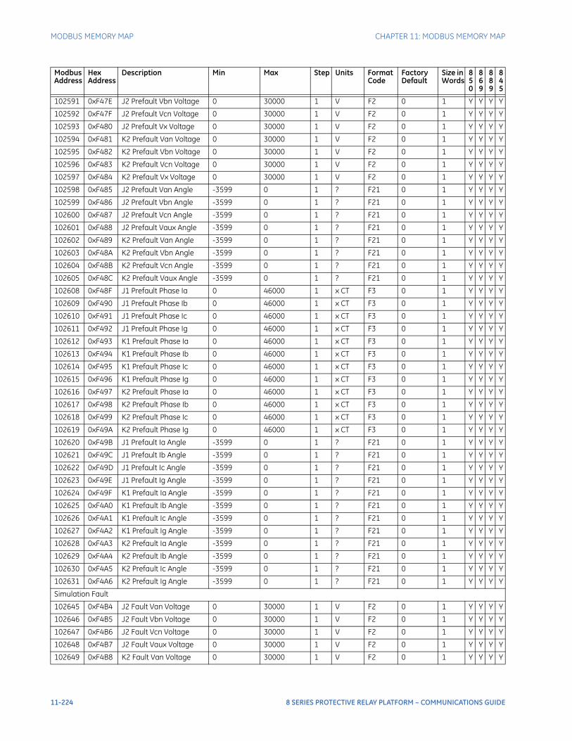
MODBUS MEMORY MAP CHAPTER 11: MODBUS MEMORY MAP
102591 0xF47E J2 Prefault Vbn Voltage 0 30000 1 V F2 0 1 Y Y Y Y
102592 0xF47F J2 Prefault Vcn Voltage 0 30000 1 V F2 0 1 Y Y Y Y
102593 0xF480 J2 Prefault Vx Voltage 0 30000 1 V F2 0 1 Y Y Y Y
102594 0xF481 K2 Prefault Van Voltage 0 30000 1 V F2 0 1 Y Y Y Y
102595 0xF482 K2 Prefault Vbn Voltage 0 30000 1 V F2 0 1 Y Y Y Y
102596 0xF483 K2 Prefault Vcn Voltage 0 30000 1 V F2 0 1 Y Y Y Y
102597 0xF484 K2 Prefault Vx Voltage 0 30000 1 V F2 0 1 Y Y Y Y
102598 0xF485 J2 Prefault Van Angle -3599 0 1 ? F21 0 1 Y Y Y Y
102599 0xF486 J2 Prefault Vbn Angle -3599 0 1 ? F21 0 1 Y Y Y Y
102600 0xF487 J2 Prefault Vcn Angle -3599 0 1 ? F21 0 1 Y Y Y Y
102601 0xF488 J2 Prefault Vaux Angle -3599 0 1 ? F21 0 1 Y Y Y Y
102602 0xF489 K2 Prefault Van Angle -3599 0 1 ? F21 0 1 Y Y Y Y
102603 0xF48A K2 Prefault Vbn Angle -3599 0 1 ? F21 0 1 Y Y Y Y
102604 0xF48B K2 Prefault Vcn Angle -3599 0 1 ? F21 0 1 Y Y Y Y
102605 0xF48C K2 Prefault Vaux Angle -3599 0 1 ? F21 0 1 Y Y Y Y
102608 0xF48F J1 Prefault Phase Ia 0 46000 1 x CT F3 0 1 Y Y Y Y
102609 0xF490 J1 Prefault Phase Ib 0 46000 1 x CT F3 0 1 Y Y Y Y
102610 0xF491 J1 Prefault Phase Ic 0 46000 1 x CT F3 0 1 Y Y Y Y
102611 0xF492 J1 Prefault Phase Ig 0 46000 1 x CT F3 0 1 Y Y Y Y
102612 0xF493 K1 Prefault Phase Ia 0 46000 1 x CT F3 0 1 Y Y Y Y
102613 0xF494 K1 Prefault Phase Ib 0 46000 1 x CT F3 0 1 Y Y Y Y
102614 0xF495 K1 Prefault Phase Ic 0 46000 1 x CT F3 0 1 Y Y Y Y
102615 0xF496 K1 Prefault Phase Ig 0 46000 1 x CT F3 0 1 Y Y Y Y
102616 0xF497 K2 Prefault Phase Ia 0 46000 1 x CT F3 0 1 Y Y Y Y
102617 0xF498 K2 Prefault Phase Ib 0 46000 1 x CT F3 0 1 Y Y Y Y
102618 0xF499 K2 Prefault Phase Ic 0 46000 1 x CT F3 0 1 Y Y Y Y
102619 0xF49A K2 Prefault Phase Ig 0 46000 1 x CT F3 0 1 Y Y Y Y
102620 0xF49B J1 Prefault Ia Angle -3599 0 1 ? F21 0 1 Y Y Y Y
102621 0xF49C J1 Prefault Ib Angle -3599 0 1 ? F21 0 1 Y Y Y Y
102622 0xF49D J1 Prefault Ic Angle -3599 0 1 ? F21 0 1 Y Y Y Y
102623 0xF49E J1 Prefault Ig Angle -3599 0 1 ? F21 0 1 Y Y Y Y
102624 0xF49F K1 Prefault Ia Angle -3599 0 1 ? F21 0 1 Y Y Y Y
102625 0xF4A0 K1 Prefault Ib Angle -3599 0 1 ? F21 0 1 Y Y Y Y
102626 0xF4A1 K1 Prefault Ic Angle -3599 0 1 ? F21 0 1 Y Y Y Y
102627 0xF4A2 K1 Prefault Ig Angle -3599 0 1 ? F21 0 1 Y Y Y Y
102628 0xF4A3 K2 Prefault Ia Angle -3599 0 1 ? F21 0 1 Y Y Y Y
102629 0xF4A4 K2 Prefault Ib Angle -3599 0 1 ? F21 0 1 Y Y Y Y
102630 0xF4A5 K2 Prefault Ic Angle -3599 0 1 ? F21 0 1 Y Y Y Y
102631 0xF4A6 K2 Prefault Ig Angle -3599 0 1 ? F21 0 1 Y Y Y Y
Simulation Fault
102645 0xF4B4 J2 Fault Van Voltage 0 30000 1 V F2 0 1 Y Y Y Y
102646 0xF4B5 J2 Fault Vbn Voltage 0 30000 1 V F2 0 1 Y Y Y Y
102647 0xF4B6 J2 Fault Vcn Voltage 0 30000 1 V F2 0 1 Y Y Y Y
102648 0xF4B7 J2 Fault Vaux Voltage 0 30000 1 V F2 0 1 Y Y Y Y
102649 0xF4B8 K2 Fault Van Voltage 0 30000 1 V F2 0 1 Y Y Y Y
Modbus Address
Hex Address
Description Min Max Step Units Format Code
Factory Default
Size in Words
850
869
889
845
11-224 8 SERIES PROTECTIVE RELAY PLATFORM – COMMUNICATIONS GUIDE
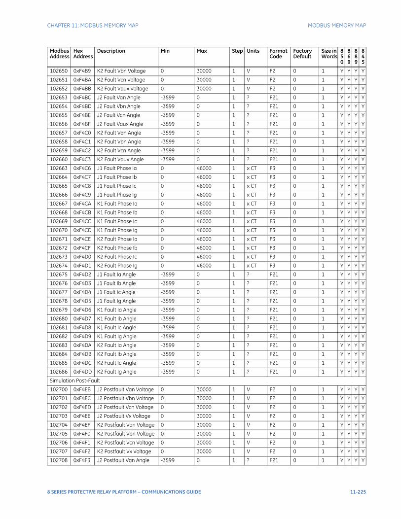
CHAPTER 11: MODBUS MEMORY MAP MODBUS MEMORY MAP
102650 0xF4B9 K2 Fault Vbn Voltage 0 30000 1 V F2 0 1 Y Y Y Y
102651 0xF4BA K2 Fault Vcn Voltage 0 30000 1 V F2 0 1 Y Y Y Y
102652 0xF4BB K2 Fault Vaux Voltage 0 30000 1 V F2 0 1 Y Y Y Y
102653 0xF4BC J2 Fault Van Angle -3599 0 1 ? F21 0 1 Y Y Y Y
102654 0xF4BD J2 Fault Vbn Angle -3599 0 1 ? F21 0 1 Y Y Y Y
102655 0xF4BE J2 Fault Vcn Angle -3599 0 1 ? F21 0 1 Y Y Y Y
102656 0xF4BF J2 Fault Vaux Angle -3599 0 1 ? F21 0 1 Y Y Y Y
102657 0xF4C0 K2 Fault Van Angle -3599 0 1 ? F21 0 1 Y Y Y Y
102658 0xF4C1 K2 Fault Vbn Angle -3599 0 1 ? F21 0 1 Y Y Y Y
102659 0xF4C2 K2 Fault Vcn Angle -3599 0 1 ? F21 0 1 Y Y Y Y
102660 0xF4C3 K2 Fault Vaux Angle -3599 0 1 ? F21 0 1 Y Y Y Y
102663 0xF4C6 J1 Fault Phase Ia 0 46000 1 x CT F3 0 1 Y Y Y Y
102664 0xF4C7 J1 Fault Phase Ib 0 46000 1 x CT F3 0 1 Y Y Y Y
102665 0xF4C8 J1 Fault Phase Ic 0 46000 1 x CT F3 0 1 Y Y Y Y
102666 0xF4C9 J1 Fault Phase Ig 0 46000 1 x CT F3 0 1 Y Y Y Y
102667 0xF4CA K1 Fault Phase Ia 0 46000 1 x CT F3 0 1 Y Y Y Y
102668 0xF4CB K1 Fault Phase Ib 0 46000 1 x CT F3 0 1 Y Y Y Y
102669 0xF4CC K1 Fault Phase Ic 0 46000 1 x CT F3 0 1 Y Y Y Y
102670 0xF4CD K1 Fault Phase Ig 0 46000 1 x CT F3 0 1 Y Y Y Y
102671 0xF4CE K2 Fault Phase Ia 0 46000 1 x CT F3 0 1 Y Y Y Y
102672 0xF4CF K2 Fault Phase Ib 0 46000 1 x CT F3 0 1 Y Y Y Y
102673 0xF4D0 K2 Fault Phase Ic 0 46000 1 x CT F3 0 1 Y Y Y Y
102674 0xF4D1 K2 Fault Phase Ig 0 46000 1 x CT F3 0 1 Y Y Y Y
102675 0xF4D2 J1 Fault Ia Angle -3599 0 1 ? F21 0 1 Y Y Y Y
102676 0xF4D3 J1 Fault Ib Angle -3599 0 1 ? F21 0 1 Y Y Y Y
102677 0xF4D4 J1 Fault Ic Angle -3599 0 1 ? F21 0 1 Y Y Y Y
102678 0xF4D5 J1 Fault Ig Angle -3599 0 1 ? F21 0 1 Y Y Y Y
102679 0xF4D6 K1 Fault Ia Angle -3599 0 1 ? F21 0 1 Y Y Y Y
102680 0xF4D7 K1 Fault Ib Angle -3599 0 1 ? F21 0 1 Y Y Y Y
102681 0xF4D8 K1 Fault Ic Angle -3599 0 1 ? F21 0 1 Y Y Y Y
102682 0xF4D9 K1 Fault Ig Angle -3599 0 1 ? F21 0 1 Y Y Y Y
102683 0xF4DA K2 Fault Ia Angle -3599 0 1 ? F21 0 1 Y Y Y Y
102684 0xF4DB K2 Fault Ib Angle -3599 0 1 ? F21 0 1 Y Y Y Y
102685 0xF4DC K2 Fault Ic Angle -3599 0 1 ? F21 0 1 Y Y Y Y
102686 0xF4DD K2 Fault Ig Angle -3599 0 1 ? F21 0 1 Y Y Y Y
Simulation Post-Fault
102700 0xF4EB J2 Postfault Van Voltage 0 30000 1 V F2 0 1 Y Y Y Y
102701 0xF4EC J2 Postfault Vbn Voltage 0 30000 1 V F2 0 1 Y Y Y Y
102702 0xF4ED J2 Postfault Vcn Voltage 0 30000 1 V F2 0 1 Y Y Y Y
102703 0xF4EE J2 Postfault Vx Voltage 0 30000 1 V F2 0 1 Y Y Y Y
102704 0xF4EF K2 Postfault Van Voltage 0 30000 1 V F2 0 1 Y Y Y Y
102705 0xF4F0 K2 Postfault Vbn Voltage 0 30000 1 V F2 0 1 Y Y Y Y
102706 0xF4F1 K2 Postfault Vcn Voltage 0 30000 1 V F2 0 1 Y Y Y Y
102707 0xF4F2 K2 Postfault Vx Voltage 0 30000 1 V F2 0 1 Y Y Y Y
102708 0xF4F3 J2 Postfault Van Angle -3599 0 1 ? F21 0 1 Y Y Y Y
Modbus Address
Hex Address
Description Min Max Step Units Format Code
Factory Default
Size in Words
850
869
889
845
8 SERIES PROTECTIVE RELAY PLATFORM – COMMUNICATIONS GUIDE 11-225
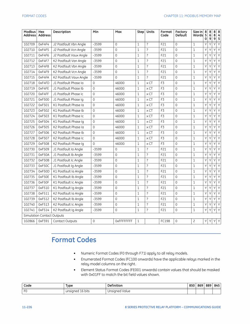
FORMAT CODES CHAPTER 11: MODBUS MEMORY MAP
Format Codes
• Numeric Format Codes (F0 through F71) apply to all relay models.
• Enumerated Format Codes (FC100 onwards) have the applicable relays marked in the relay model columns on the right.
• Element Status Format Codes (FE001 onwards) contain values that should be masked with 0x01FF to match the bit field values shown.
102709 0xF4F4 J2 Postfault Vbn Angle -3599 0 1 ? F21 0 1 Y Y Y Y
102710 0xF4F5 J2 Postfault Vcn Angle -3599 0 1 ? F21 0 1 Y Y Y Y
102711 0xF4F6 J2 Postfault Vaux Angle -3599 0 1 ? F21 0 1 Y Y Y Y
102712 0xF4F7 K2 Postfault Van Angle -3599 0 1 ? F21 0 1 Y Y Y Y
102713 0xF4F8 K2 Postfault Vbn Angle -3599 0 1 ? F21 0 1 Y Y Y Y
102714 0xF4F9 K2 Postfault Vcn Angle -3599 0 1 ? F21 0 1 Y Y Y Y
102715 0xF4FA K2 Postfault Vaux Angle -3599 0 1 ? F21 0 1 Y Y Y Y
102718 0xF4FD J1 Postfault Phase Ia 0 46000 1 x CT F3 0 1 Y Y Y Y
102719 0xF4FE J1 Postfault Phase Ib 0 46000 1 x CT F3 0 1 Y Y Y Y
102720 0xF4FF J1 Postfault Phase Ic 0 46000 1 x CT F3 0 1 Y Y Y Y
102721 0xF500 J1 Postfault Phase Ig 0 46000 1 x CT F3 0 1 Y Y Y Y
102722 0xF501 K1 Postfault Phase Ia 0 46000 1 x CT F3 0 1 Y Y Y Y
102723 0xF502 K1 Postfault Phase Ib 0 46000 1 x CT F3 0 1 Y Y Y Y
102724 0xF503 K1 Postfault Phase Ic 0 46000 1 x CT F3 0 1 Y Y Y Y
102725 0xF504 K1 Postfault Phase Ig 0 46000 1 x CT F3 0 1 Y Y Y Y
102726 0xF505 K2 Postfault Phase Ia 0 46000 1 x CT F3 0 1 Y Y Y Y
102727 0xF506 K2 Postfault Phase Ib 0 46000 1 x CT F3 0 1 Y Y Y Y
102728 0xF507 K2 Postfault Phase Ic 0 46000 1 x CT F3 0 1 Y Y Y Y
102729 0xF508 K2 Postfault Phase Ig 0 46000 1 x CT F3 0 1 Y Y Y Y
102730 0xF509 J1 Postfault Ia Angle -3599 0 1 ? F21 0 1 Y Y Y Y
102731 0xF50A J1 Postfault Ib Angle -3599 0 1 ? F21 0 1 Y Y Y Y
102732 0xF50B J1 Postfault Ic Angle -3599 0 1 ? F21 0 1 Y Y Y Y
102733 0xF50C J1 Postfault Ig Angle -3599 0 1 ? F21 0 1 Y Y Y Y
102734 0xF50D K1 Postfault Ia Angle -3599 0 1 ? F21 0 1 Y Y Y Y
102735 0xF50E K1 Postfault Ib Angle -3599 0 1 ? F21 0 1 Y Y Y Y
102736 0xF50F K1 Postfault Ic Angle -3599 0 1 ? F21 0 1 Y Y Y Y
102737 0xF510 K1 Postfault Ig Angle -3599 0 1 ? F21 0 1 Y Y Y Y
102738 0xF511 K2 Postfault Ia Angle -3599 0 1 ? F21 0 1 Y Y Y Y
102739 0xF512 K2 Postfault Ib Angle -3599 0 1 ? F21 0 1 Y Y Y Y
102740 0xF513 K2 Postfault Ic Angle -3599 0 1 ? F21 0 1 Y Y Y Y
102741 0xF514 K2 Postfault Ig Angle -3599 0 1 ? F21 0 1 Y Y Y Y
Simulation Contact Outputs
102866 0xF591 Contact Outputs 0 0xFFFFFFFF 1 FC198 0 2 Y Y Y Y
Modbus Address
Hex Address
Description Min Max Step Units Format Code
Factory Default
Size in Words
850
869
889
845
Code Type Definition 850 869 889 845
F0 unsigned 16 bits Unsigned Value
11-226 8 SERIES PROTECTIVE RELAY PLATFORM – COMMUNICATIONS GUIDE
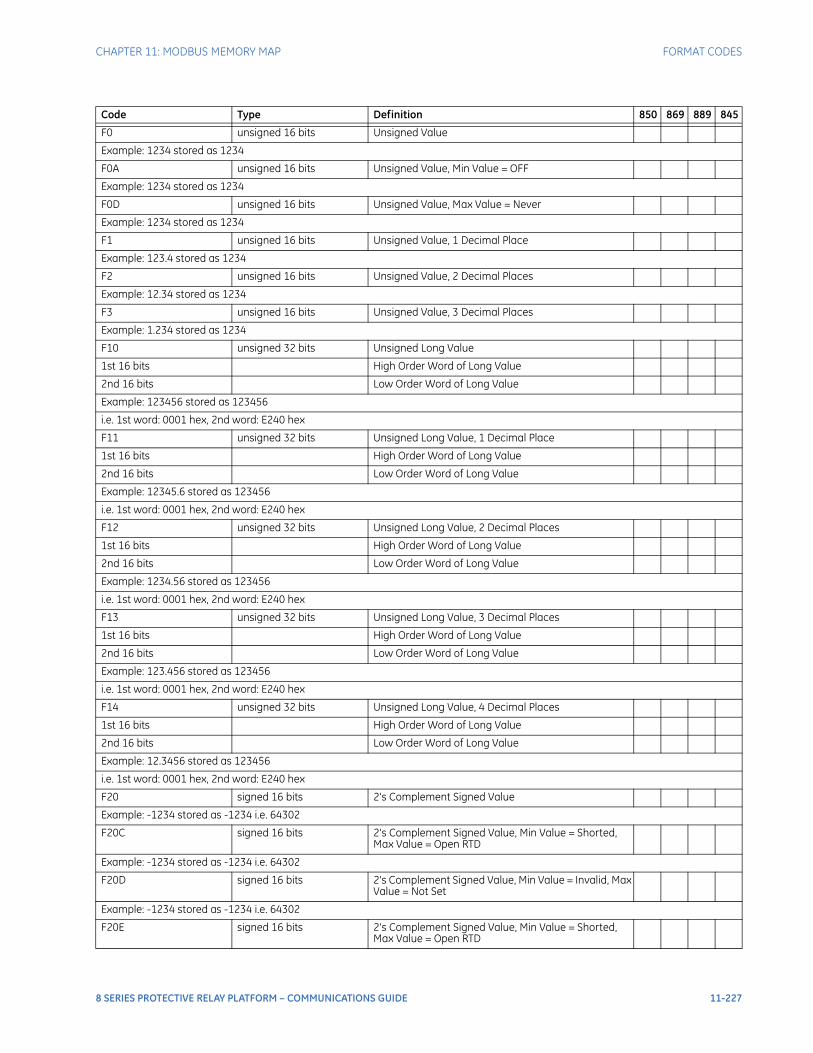
CHAPTER 11: MODBUS MEMORY MAP FORMAT CODES
Code Type Definition 850 869 889 845
F0 unsigned 16 bits Unsigned Value
Example: 1234 stored as 1234
F0A unsigned 16 bits Unsigned Value, Min Value = OFF
Example: 1234 stored as 1234
F0D unsigned 16 bits Unsigned Value, Max Value = Never
Example: 1234 stored as 1234
F1 unsigned 16 bits Unsigned Value, 1 Decimal Place
Example: 123.4 stored as 1234
F2 unsigned 16 bits Unsigned Value, 2 Decimal Places
Example: 12.34 stored as 1234
F3 unsigned 16 bits Unsigned Value, 3 Decimal Places
Example: 1.234 stored as 1234
F10 unsigned 32 bits Unsigned Long Value
1st 16 bits High Order Word of Long Value
2nd 16 bits Low Order Word of Long Value
Example: 123456 stored as 123456
i.e. 1st word: 0001 hex, 2nd word: E240 hex
F11 unsigned 32 bits Unsigned Long Value, 1 Decimal Place
1st 16 bits High Order Word of Long Value
2nd 16 bits Low Order Word of Long Value
Example: 12345.6 stored as 123456
i.e. 1st word: 0001 hex, 2nd word: E240 hex
F12 unsigned 32 bits Unsigned Long Value, 2 Decimal Places
1st 16 bits High Order Word of Long Value
2nd 16 bits Low Order Word of Long Value
Example: 1234.56 stored as 123456
i.e. 1st word: 0001 hex, 2nd word: E240 hex
F13 unsigned 32 bits Unsigned Long Value, 3 Decimal Places
1st 16 bits High Order Word of Long Value
2nd 16 bits Low Order Word of Long Value
Example: 123.456 stored as 123456
i.e. 1st word: 0001 hex, 2nd word: E240 hex
F14 unsigned 32 bits Unsigned Long Value, 4 Decimal Places
1st 16 bits High Order Word of Long Value
2nd 16 bits Low Order Word of Long Value
Example: 12.3456 stored as 123456
i.e. 1st word: 0001 hex, 2nd word: E240 hex
F20 signed 16 bits 2's Complement Signed Value
Example: -1234 stored as -1234 i.e. 64302
F20C signed 16 bits 2's Complement Signed Value, Min Value = Shorted, Max Value = Open RTD
Example: -1234 stored as -1234 i.e. 64302
F20D signed 16 bits 2's Complement Signed Value, Min Value = Invalid, Max Value = Not Set
Example: -1234 stored as -1234 i.e. 64302
F20E signed 16 bits 2's Complement Signed Value, Min Value = Shorted, Max Value = Open RTD
8 SERIES PROTECTIVE RELAY PLATFORM – COMMUNICATIONS GUIDE 11-227
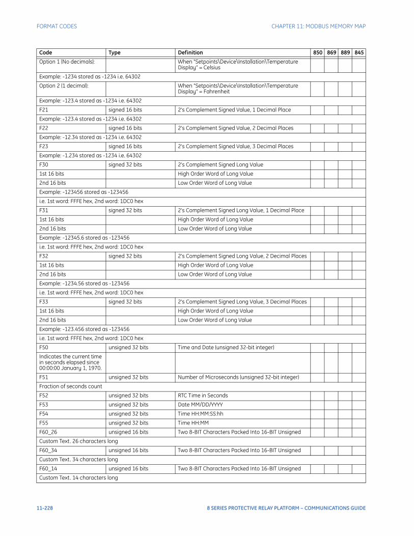
FORMAT CODES CHAPTER 11: MODBUS MEMORY MAP
Option 1 (No decimals): When "Setpoints\Device\Installation\Temperature Display” = Celsius
Example: -1234 stored as -1234 i.e. 64302
Option 2 (1 decimal): When "Setpoints\Device\Installation\Temperature Display” = Fahrenheit
Example: -123.4 stored as -1234 i.e. 64302
F21 signed 16 bits 2's Complement Signed Value, 1 Decimal Place
Example: -123.4 stored as -1234 i.e. 64302
F22 signed 16 bits 2's Complement Signed Value, 2 Decimal Places
Example: -12.34 stored as -1234 i.e. 64302
F23 signed 16 bits 2's Complement Signed Value, 3 Decimal Places
Example: -1.234 stored as -1234 i.e. 64302
F30 signed 32 bits 2's Complement Signed Long Value
1st 16 bits High Order Word of Long Value
2nd 16 bits Low Order Word of Long Value
Example: -123456 stored as -123456
i.e. 1st word: FFFE hex, 2nd word: 1DC0 hex
F31 signed 32 bits 2's Complement Signed Long Value, 1 Decimal Place
1st 16 bits High Order Word of Long Value
2nd 16 bits Low Order Word of Long Value
Example: -12345.6 stored as -123456
i.e. 1st word: FFFE hex, 2nd word: 1DC0 hex
F32 signed 32 bits 2's Complement Signed Long Value, 2 Decimal Places
1st 16 bits High Order Word of Long Value
2nd 16 bits Low Order Word of Long Value
Example: -1234.56 stored as -123456
i.e. 1st word: FFFE hex, 2nd word: 1DC0 hex
F33 signed 32 bits 2's Complement Signed Long Value, 3 Decimal Places
1st 16 bits High Order Word of Long Value
2nd 16 bits Low Order Word of Long Value
Example: -123.456 stored as -123456
i.e. 1st word: FFFE hex, 2nd word: 1DC0 hex
F50 unsigned 32 bits Time and Date (unsigned 32-bit integer)
Indicates the current time in seconds elapsed since 00:00:00 January 1, 1970.
F51 unsigned 32 bits Number of Microseconds (unsigned 32-bit integer)
Fraction of seconds count
F52 unsigned 32 bits RTC Time in Seconds
F53 unsigned 32 bits Date MM/DD/YYYY
F54 unsigned 32 bits Time HH:MM:SS:hh
F55 unsigned 32 bits Time HH:MM
F60_26 unsigned 16 bits Two 8-BIT Characters Packed Into 16-BIT Unsigned
Custom Text. 26 characters long
F60_34 unsigned 16 bits Two 8-BIT Characters Packed Into 16-BIT Unsigned
Custom Text. 34 characters long
F60_14 unsigned 16 bits Two 8-BIT Characters Packed Into 16-BIT Unsigned
Custom Text. 14 characters long
Code Type Definition 850 869 889 845
11-228 8 SERIES PROTECTIVE RELAY PLATFORM – COMMUNICATIONS GUIDE
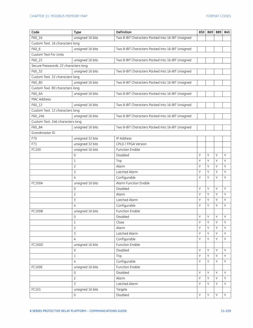
CHAPTER 11: MODBUS MEMORY MAP FORMAT CODES
F60_16 unsigned 16 bits Two 8-BIT Characters Packed Into 16-BIT Unsigned
Custom Text. 16 characters long
F60_6 unsigned 16 bits Two 8-BIT Characters Packed Into 16-BIT Unsigned
Custom Text For Units
F60_22 unsigned 16 bits Two 8-BIT Characters Packed Into 16-BIT Unsigned
Secure Passwords. 22 characters long
F60_32 unsigned 16 bits Two 8-BIT Characters Packed Into 16-BIT Unsigned
Custom Text. 32 characters long
F60_80 unsigned 16 bits Two 8-BIT Characters Packed Into 16-BIT Unsigned
Custom Text. 80 characters long
F60_6A unsigned 16 bits Two 8-BIT Characters Packed Into 16-BIT Unsigned
MAC Address
F60_12 unsigned 16 bits Two 8-BIT Characters Packed Into 16-BIT Unsigned
Custom Text. 12 characters long
F60_246 unsigned 16 bits Two 8-BIT Characters Packed Into 16-BIT Unsigned
Custom Text. 246 characters long
F60_8A unsigned 16 bits Two 8-BIT Characters Packed Into 16-BIT Unsigned
Grandmaster ID
F70 unsigned 32 bits IP Address
F71 unsigned 32 bits CPLD / FPGA Version
FC100 unsigned 16 bits Function Enable
0 Disabled Y Y Y Y
1 Trip Y Y Y Y
2 Alarm Y Y Y Y
3 Latched Alarm Y Y Y Y
4 Configurable Y Y Y Y
FC100A unsigned 16 bits Alarm Function Enable
0 Disabled Y Y Y Y
2 Alarm Y Y Y Y
3 Latched Alarm Y Y Y Y
4 Configurable Y Y Y Y
FC100B unsigned 16 bits Function Enable
0 Disabled Y Y Y Y
1 Close Y Y Y Y
2 Alarm Y Y Y Y
3 Latched Alarm Y Y Y Y
4 Configurable Y Y Y Y
FC100D unsigned 16 bits Function Enable
0 Disabled Y Y Y Y
1 Trip Y Y Y Y
4 Configurable Y Y Y Y
FC100E unsigned 16 bits Function Enable
0 Disabled Y Y Y Y
2 Alarm Y Y Y Y
3 Latched Alarm Y Y Y Y
FC101 unsigned 16 bits Targets
0 Disabled Y Y Y Y
Code Type Definition 850 869 889 845
8 SERIES PROTECTIVE RELAY PLATFORM – COMMUNICATIONS GUIDE 11-229
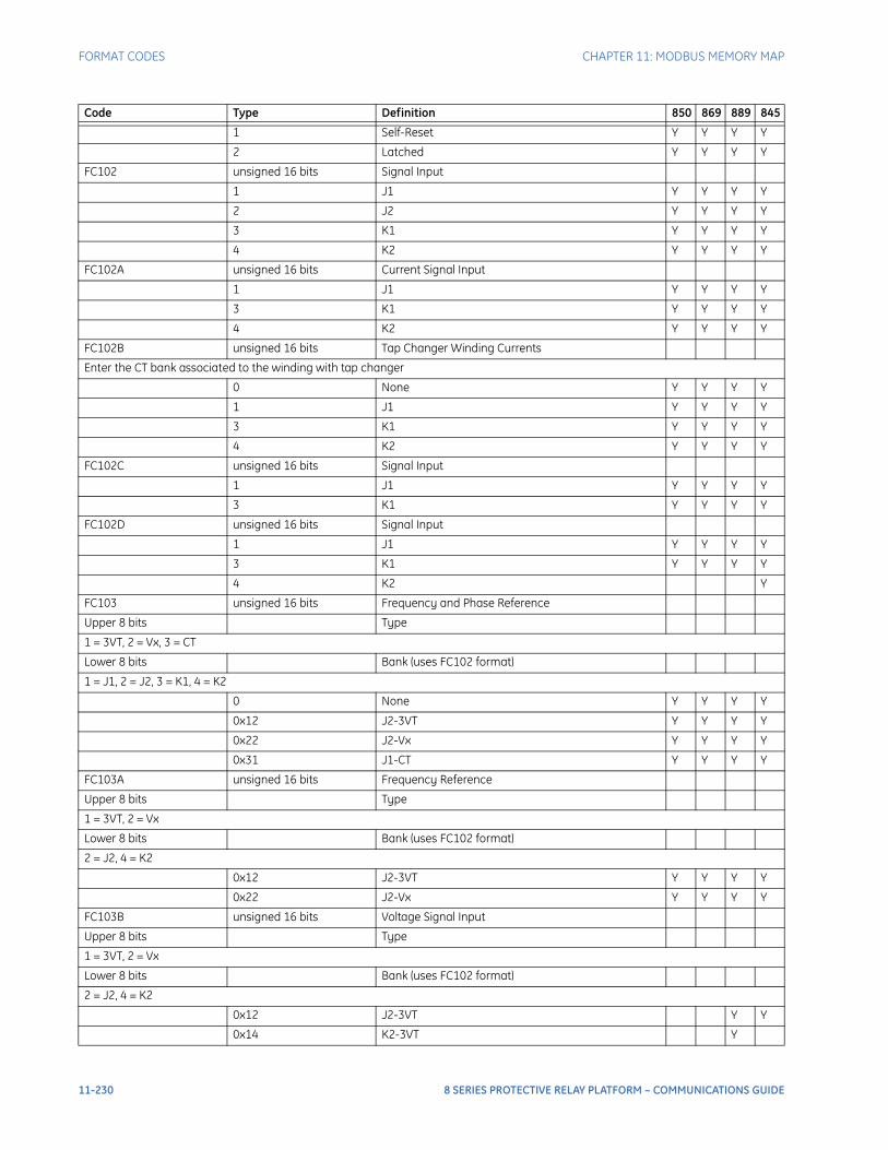
FORMAT CODES CHAPTER 11: MODBUS MEMORY MAP
1 Self-Reset Y Y Y Y
2 Latched Y Y Y Y
FC102 unsigned 16 bits Signal Input
1 J1 Y Y Y Y
2 J2 Y Y Y Y
3 K1 Y Y Y Y
4 K2 Y Y Y Y
FC102A unsigned 16 bits Current Signal Input
1 J1 Y Y Y Y
3 K1 Y Y Y Y
4 K2 Y Y Y Y
FC102B unsigned 16 bits Tap Changer Winding Currents
Enter the CT bank associated to the winding with tap changer
0 None Y Y Y Y
1 J1 Y Y Y Y
3 K1 Y Y Y Y
4 K2 Y Y Y Y
FC102C unsigned 16 bits Signal Input
1 J1 Y Y Y Y
3 K1 Y Y Y Y
FC102D unsigned 16 bits Signal Input
1 J1 Y Y Y Y
3 K1 Y Y Y Y
4 K2 Y
FC103 unsigned 16 bits Frequency and Phase Reference
Upper 8 bits Type
1 = 3VT, 2 = Vx, 3 = CT
Lower 8 bits Bank (uses FC102 format)
1 = J1, 2 = J2, 3 = K1, 4 = K2
0 None Y Y Y Y
0x12 J2-3VT Y Y Y Y
0x22 J2-Vx Y Y Y Y
0x31 J1-CT Y Y Y Y
FC103A unsigned 16 bits Frequency Reference
Upper 8 bits Type
1 = 3VT, 2 = Vx
Lower 8 bits Bank (uses FC102 format)
2 = J2, 4 = K2
0x12 J2-3VT Y Y Y Y
0x22 J2-Vx Y Y Y Y
FC103B unsigned 16 bits Voltage Signal Input
Upper 8 bits Type
1 = 3VT, 2 = Vx
Lower 8 bits Bank (uses FC102 format)
2 = J2, 4 = K2
0x12 J2-3VT Y Y
0x14 K2-3VT Y
Code Type Definition 850 869 889 845
11-230 8 SERIES PROTECTIVE RELAY PLATFORM – COMMUNICATIONS GUIDE
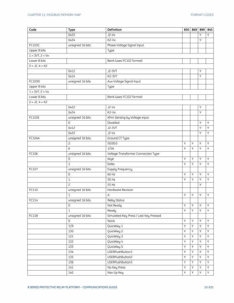
CHAPTER 11: MODBUS MEMORY MAP FORMAT CODES
0x22 J2-Vx Y Y
0x24 K2-Vx Y
FC103C unsigned 16 bits Phase Voltage Signal Input
Upper 8 bits Type
1 = 3VT, 2 = Vx
Lower 8 bits Bank (uses FC102 format)
2 = J2, 4 = K2
0x12 J2-3VT Y
0x14 K2-3VT Y
FC103D unsigned 16 bits Aux Voltage Signal Input
Upper 8 bits Type
1 = 3VT, 2 = Vx
Lower 8 bits Bank (uses FC102 format)
2 = J2, 4 = K2
0x22 J2-Vx Y
0x24 K2-Vx Y
FC103E unsigned 16 bits Xfmr Sensing by Voltage Input
0 Disabled Y Y
0x12 J2-3VT Y Y
0x22 J2-Vx Y Y
FC104A unsigned 16 bits Ground CT Type
2 50:00.0 Y Y Y Y
6 1/5A Y Y Y Y
FC106 unsigned 16 bits Voltage Transformer Connection Type
0 Wye Y Y Y Y
1 Delta Y Y Y Y
FC107 unsigned 16 bits Supply Frequency
0 60 Hz Y Y Y Y
1 50 Hz Y Y Y Y
2 25 Hz Y
FC110 unsigned 16 bits Hardware Revision
1 A Y Y Y Y
FC114 unsigned 16 bits Relay Status
0 Not Ready Y Y Y Y
1 Ready Y Y Y Y
FC118 unsigned 16 bits Simulated Key Press / Last Key Pressed
0 None Y Y Y Y
129 QuickKey 1 Y Y Y Y
130 QuickKey 2 Y Y Y Y
131 QuickKey 3 Y Y Y Y
132 QuickKey 4 Y Y Y Y
133 QuickKey 5 Y Y Y Y
134 USERPushButton1 Y Y Y Y
135 USERPushButton2 Y Y Y Y
136 USERPushButton3 Y Y Y Y
141 No Key Press Y Y Y Y
142 Nav Up Key Y Y Y Y
Code Type Definition 850 869 889 845
8 SERIES PROTECTIVE RELAY PLATFORM – COMMUNICATIONS GUIDE 11-231
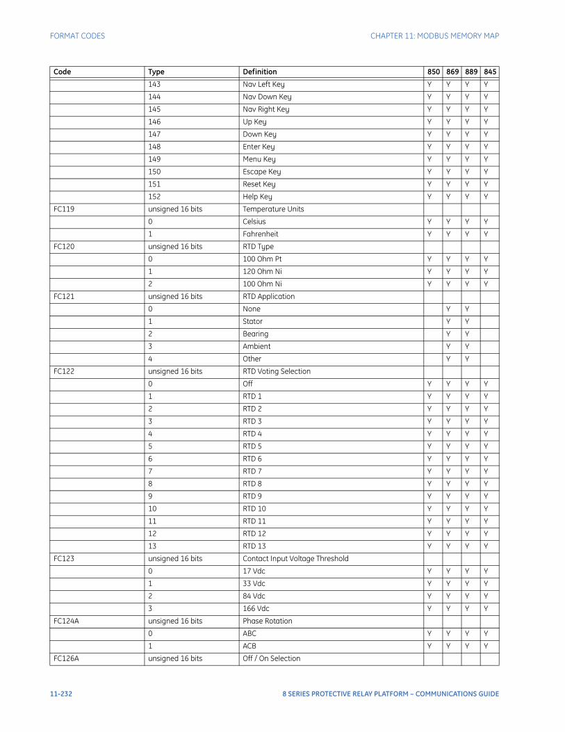
FORMAT CODES CHAPTER 11: MODBUS MEMORY MAP
143 Nav Left Key Y Y Y Y
144 Nav Down Key Y Y Y Y
145 Nav Right Key Y Y Y Y
146 Up Key Y Y Y Y
147 Down Key Y Y Y Y
148 Enter Key Y Y Y Y
149 Menu Key Y Y Y Y
150 Escape Key Y Y Y Y
151 Reset Key Y Y Y Y
152 Help Key Y Y Y Y
FC119 unsigned 16 bits Temperature Units
0 Celsius Y Y Y Y
1 Fahrenheit Y Y Y Y
FC120 unsigned 16 bits RTD Type
0 100 Ohm Pt Y Y Y Y
1 120 Ohm Ni Y Y Y Y
2 100 Ohm Ni Y Y Y Y
FC121 unsigned 16 bits RTD Application
0 None Y Y
1 Stator Y Y
2 Bearing Y Y
3 Ambient Y Y
4 Other Y Y
FC122 unsigned 16 bits RTD Voting Selection
0 Off Y Y Y Y
1 RTD 1 Y Y Y Y
2 RTD 2 Y Y Y Y
3 RTD 3 Y Y Y Y
4 RTD 4 Y Y Y Y
5 RTD 5 Y Y Y Y
6 RTD 6 Y Y Y Y
7 RTD 7 Y Y Y Y
8 RTD 8 Y Y Y Y
9 RTD 9 Y Y Y Y
10 RTD 10 Y Y Y Y
11 RTD 11 Y Y Y Y
12 RTD 12 Y Y Y Y
13 RTD 13 Y Y Y Y
FC123 unsigned 16 bits Contact Input Voltage Threshold
0 17 Vdc Y Y Y Y
1 33 Vdc Y Y Y Y
2 84 Vdc Y Y Y Y
3 166 Vdc Y Y Y Y
FC124A unsigned 16 bits Phase Rotation
0 ABC Y Y Y Y
1 ACB Y Y Y Y
FC126A unsigned 16 bits Off / On Selection
Code Type Definition 850 869 889 845
11-232 8 SERIES PROTECTIVE RELAY PLATFORM – COMMUNICATIONS GUIDE
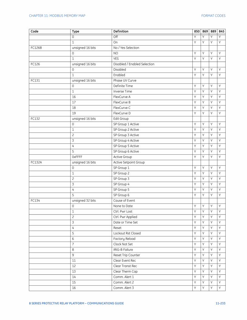
CHAPTER 11: MODBUS MEMORY MAP FORMAT CODES
0 Off Y Y Y Y
1 On Y Y Y Y
FC126B unsigned 16 bits No / Yes Selection
0 NO Y Y Y Y
1 YES Y Y Y Y
FC126 unsigned 16 bits Disabled / Enabled Selection
0 Disabled Y Y Y Y
1 Enabled Y Y Y Y
FC131 unsigned 16 bits Phase UV Curve
0 Definite Time Y Y Y Y
1 Inverse Time Y Y Y Y
16 FlexCurve A Y Y Y Y
17 FlexCurve B Y Y Y Y
18 FlexCurve C Y Y Y Y
19 FlexCurve D Y Y Y Y
FC132 unsigned 16 bits Edit Group
0 SP Group 1 Active Y Y Y Y
1 SP Group 2 Active Y Y Y Y
2 SP Group 3 Active Y Y Y Y
3 SP Group 4 Active Y Y Y Y
4 SP Group 5 Active Y Y Y Y
5 SP Group 6 Active Y Y Y Y
0xFFFF Active Group Y Y Y Y
FC132A unsigned 16 bits Active Setpoint Group
0 SP Group 1 Y Y Y Y
1 SP Group 2 Y Y Y Y
2 SP Group 3 Y Y Y Y
3 SP Group 4 Y Y Y Y
4 SP Group 5 Y Y Y Y
5 SP Group 6 Y Y Y Y
FC134 unsigned 32 bits Cause of Event
0 None to Date Y Y Y Y
1 Ctrl. Pwr Lost Y Y Y Y
2 Ctrl. Pwr Applied Y Y Y Y
3 Date or Time Set Y Y Y Y
4 Reset Y Y Y Y
5 Lockout Rst Closed Y Y Y Y
6 Factory Reload Y Y Y Y
7 Clock Not Set Y Y Y Y
8 IRIG-B Failure Y Y Y Y
9 Reset Trip Counter Y Y Y Y
11 Clear Event Rec Y Y Y Y
12 Clear Transt Rec Y Y Y Y
13 Clear Therm Cap Y Y Y Y
14 Comm. Alert 1 Y Y Y Y
15 Comm. Alert 2 Y Y Y Y
16 Comm. Alert 3 Y Y Y Y
Code Type Definition 850 869 889 845
8 SERIES PROTECTIVE RELAY PLATFORM – COMMUNICATIONS GUIDE 11-233
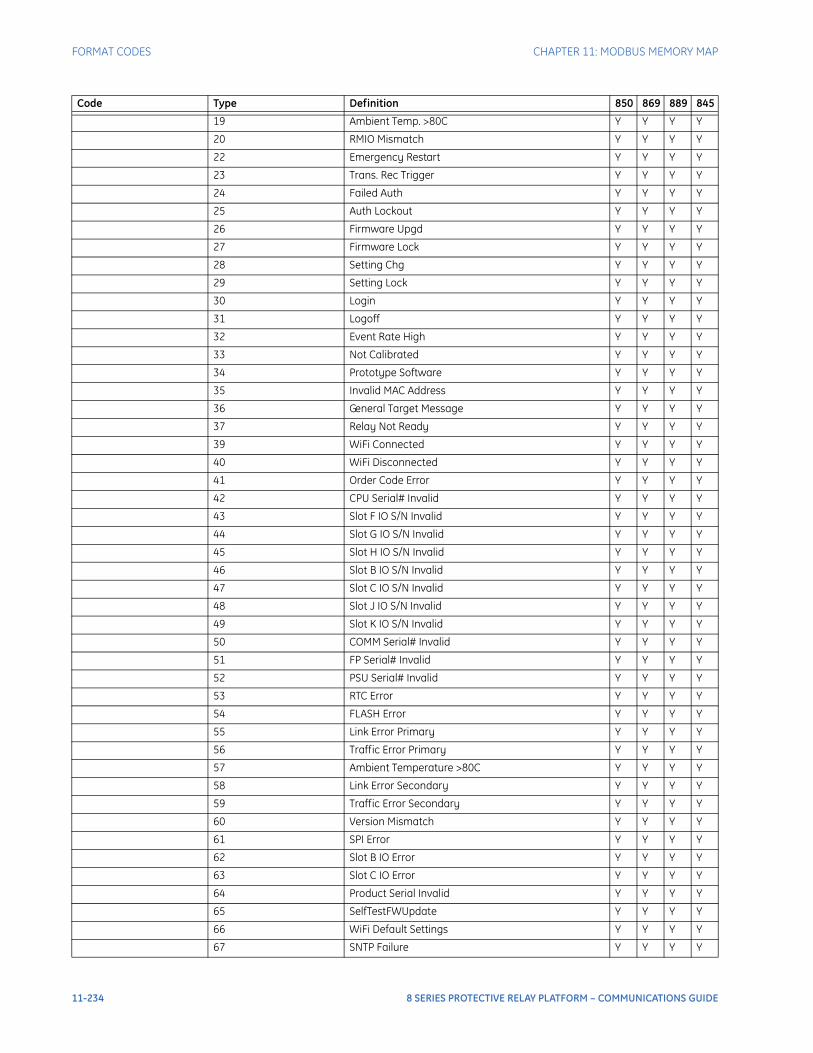
FORMAT CODES CHAPTER 11: MODBUS MEMORY MAP
19 Ambient Temp. >80C Y Y Y Y
20 RMIO Mismatch Y Y Y Y
22 Emergency Restart Y Y Y Y
23 Trans. Rec Trigger Y Y Y Y
24 Failed Auth Y Y Y Y
25 Auth Lockout Y Y Y Y
26 Firmware Upgd Y Y Y Y
27 Firmware Lock Y Y Y Y
28 Setting Chg Y Y Y Y
29 Setting Lock Y Y Y Y
30 Login Y Y Y Y
31 Logoff Y Y Y Y
32 Event Rate High Y Y Y Y
33 Not Calibrated Y Y Y Y
34 Prototype Software Y Y Y Y
35 Invalid MAC Address Y Y Y Y
36 General Target Message Y Y Y Y
37 Relay Not Ready Y Y Y Y
39 WiFi Connected Y Y Y Y
40 WiFi Disconnected Y Y Y Y
41 Order Code Error Y Y Y Y
42 CPU Serial# Invalid Y Y Y Y
43 Slot F IO S/N Invalid Y Y Y Y
44 Slot G IO S/N Invalid Y Y Y Y
45 Slot H IO S/N Invalid Y Y Y Y
46 Slot B IO S/N Invalid Y Y Y Y
47 Slot C IO S/N Invalid Y Y Y Y
48 Slot J IO S/N Invalid Y Y Y Y
49 Slot K IO S/N Invalid Y Y Y Y
50 COMM Serial# Invalid Y Y Y Y
51 FP Serial# Invalid Y Y Y Y
52 PSU Serial# Invalid Y Y Y Y
53 RTC Error Y Y Y Y
54 FLASH Error Y Y Y Y
55 Link Error Primary Y Y Y Y
56 Traffic Error Primary Y Y Y Y
57 Ambient Temperature >80C Y Y Y Y
58 Link Error Secondary Y Y Y Y
59 Traffic Error Secondary Y Y Y Y
60 Version Mismatch Y Y Y Y
61 SPI Error Y Y Y Y
62 Slot B IO Error Y Y Y Y
63 Slot C IO Error Y Y Y Y
64 Product Serial Invalid Y Y Y Y
65 SelfTestFWUpdate Y Y Y Y
66 WiFi Default Settings Y Y Y Y
67 SNTP Failure Y Y Y Y
Code Type Definition 850 869 889 845
11-234 8 SERIES PROTECTIVE RELAY PLATFORM – COMMUNICATIONS GUIDE
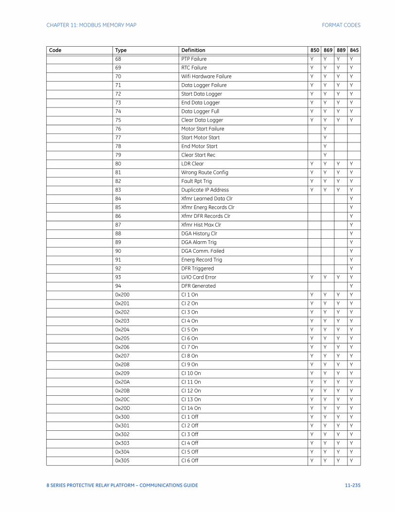
CHAPTER 11: MODBUS MEMORY MAP FORMAT CODES
68 PTP Failure Y Y Y Y
69 RTC Failure Y Y Y Y
70 Wifi Hardware Failure Y Y Y Y
71 Data Logger Failure Y Y Y Y
72 Start Data Logger Y Y Y Y
73 End Data Logger Y Y Y Y
74 Data Logger Full Y Y Y Y
75 Clear Data Logger Y Y Y Y
76 Motor Start Failure Y
77 Start Motor Start Y
78 End Motor Start Y
79 Clear Start Rec Y
80 LDR Clear Y Y Y Y
81 Wrong Route Config Y Y Y Y
82 Fault Rpt Trig Y Y Y Y
83 Duplicate IP Address Y Y Y Y
84 Xfmr Learned Data Clr Y
85 Xfmr Energ Records Clr Y
86 Xfmr DFR Records Clr Y
87 Xfmr Hist Max Clr Y
88 DGA History Clr Y
89 DGA Alarm Trig Y
90 DGA Comm. Failed Y
91 Energ Record Trig Y
92 DFR Triggered Y
93 LVIO Card Error Y Y Y Y
94 DFR Generated Y
0x200 CI 1 On Y Y Y Y
0x201 CI 2 On Y Y Y Y
0x202 CI 3 On Y Y Y Y
0x203 CI 4 On Y Y Y Y
0x204 CI 5 On Y Y Y Y
0x205 CI 6 On Y Y Y Y
0x206 CI 7 On Y Y Y Y
0x207 CI 8 On Y Y Y Y
0x208 CI 9 On Y Y Y Y
0x209 CI 10 On Y Y Y Y
0x20A CI 11 On Y Y Y Y
0x20B CI 12 On Y Y Y Y
0x20C CI 13 On Y Y Y Y
0x20D CI 14 On Y Y Y Y
0x300 CI 1 Off Y Y Y Y
0x301 CI 2 Off Y Y Y Y
0x302 CI 3 Off Y Y Y Y
0x303 CI 4 Off Y Y Y Y
0x304 CI 5 Off Y Y Y Y
0x305 CI 6 Off Y Y Y Y
Code Type Definition 850 869 889 845
8 SERIES PROTECTIVE RELAY PLATFORM – COMMUNICATIONS GUIDE 11-235
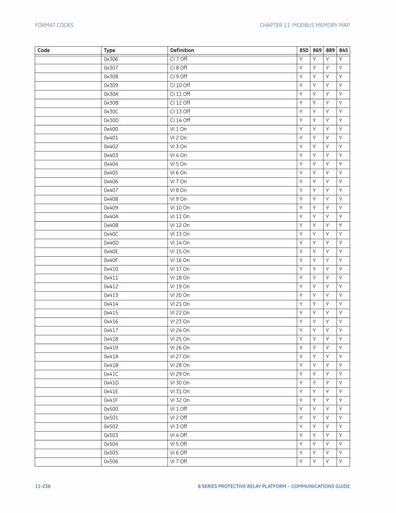
FORMAT CODES CHAPTER 11: MODBUS MEMORY MAP
0x306 CI 7 Off Y Y Y Y
0x307 CI 8 Off Y Y Y Y
0x308 CI 9 Off Y Y Y Y
0x309 CI 10 Off Y Y Y Y
0x30A CI 11 Off Y Y Y Y
0x30B CI 12 Off Y Y Y Y
0x30C CI 13 Off Y Y Y Y
0x30D CI 14 Off Y Y Y Y
0x400 VI 1 On Y Y Y Y
0x401 VI 2 On Y Y Y Y
0x402 VI 3 On Y Y Y Y
0x403 VI 4 On Y Y Y Y
0x404 VI 5 On Y Y Y Y
0x405 VI 6 On Y Y Y Y
0x406 VI 7 On Y Y Y Y
0x407 VI 8 On Y Y Y Y
0x408 VI 9 On Y Y Y Y
0x409 VI 10 On Y Y Y Y
0x40A VI 11 On Y Y Y Y
0x40B VI 12 On Y Y Y Y
0x40C VI 13 On Y Y Y Y
0x40D VI 14 On Y Y Y Y
0x40E VI 15 On Y Y Y Y
0x40F VI 16 On Y Y Y Y
0x410 VI 17 On Y Y Y Y
0x411 VI 18 On Y Y Y Y
0x412 VI 19 On Y Y Y Y
0x413 VI 20 On Y Y Y Y
0x414 VI 21 On Y Y Y Y
0x415 VI 22 On Y Y Y Y
0x416 VI 23 On Y Y Y Y
0x417 VI 24 On Y Y Y Y
0x418 VI 25 On Y Y Y Y
0x419 VI 26 On Y Y Y Y
0x41A VI 27 On Y Y Y Y
0x41B VI 28 On Y Y Y Y
0x41C VI 29 On Y Y Y Y
0x41D VI 30 On Y Y Y Y
0x41E VI 31 On Y Y Y Y
0x41F VI 32 On Y Y Y Y
0x500 VI 1 Off Y Y Y Y
0x501 VI 2 Off Y Y Y Y
0x502 VI 3 Off Y Y Y Y
0x503 VI 4 Off Y Y Y Y
0x504 VI 5 Off Y Y Y Y
0x505 VI 6 Off Y Y Y Y
0x506 VI 7 Off Y Y Y Y
Code Type Definition 850 869 889 845
11-236 8 SERIES PROTECTIVE RELAY PLATFORM – COMMUNICATIONS GUIDE
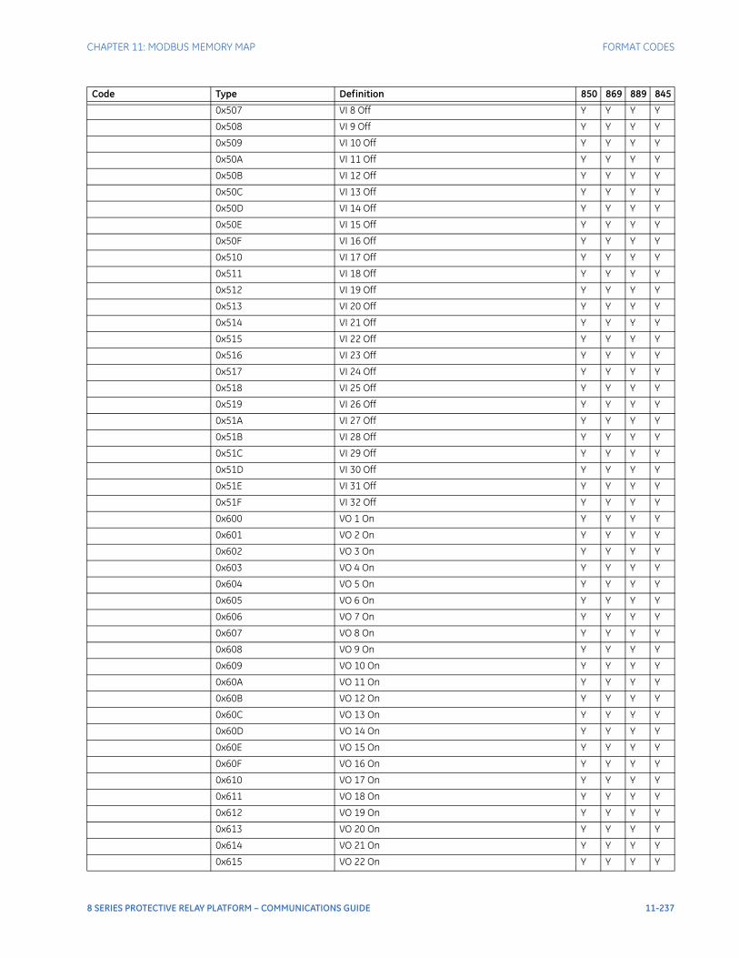
CHAPTER 11: MODBUS MEMORY MAP FORMAT CODES
0x507 VI 8 Off Y Y Y Y
0x508 VI 9 Off Y Y Y Y
0x509 VI 10 Off Y Y Y Y
0x50A VI 11 Off Y Y Y Y
0x50B VI 12 Off Y Y Y Y
0x50C VI 13 Off Y Y Y Y
0x50D VI 14 Off Y Y Y Y
0x50E VI 15 Off Y Y Y Y
0x50F VI 16 Off Y Y Y Y
0x510 VI 17 Off Y Y Y Y
0x511 VI 18 Off Y Y Y Y
0x512 VI 19 Off Y Y Y Y
0x513 VI 20 Off Y Y Y Y
0x514 VI 21 Off Y Y Y Y
0x515 VI 22 Off Y Y Y Y
0x516 VI 23 Off Y Y Y Y
0x517 VI 24 Off Y Y Y Y
0x518 VI 25 Off Y Y Y Y
0x519 VI 26 Off Y Y Y Y
0x51A VI 27 Off Y Y Y Y
0x51B VI 28 Off Y Y Y Y
0x51C VI 29 Off Y Y Y Y
0x51D VI 30 Off Y Y Y Y
0x51E VI 31 Off Y Y Y Y
0x51F VI 32 Off Y Y Y Y
0x600 VO 1 On Y Y Y Y
0x601 VO 2 On Y Y Y Y
0x602 VO 3 On Y Y Y Y
0x603 VO 4 On Y Y Y Y
0x604 VO 5 On Y Y Y Y
0x605 VO 6 On Y Y Y Y
0x606 VO 7 On Y Y Y Y
0x607 VO 8 On Y Y Y Y
0x608 VO 9 On Y Y Y Y
0x609 VO 10 On Y Y Y Y
0x60A VO 11 On Y Y Y Y
0x60B VO 12 On Y Y Y Y
0x60C VO 13 On Y Y Y Y
0x60D VO 14 On Y Y Y Y
0x60E VO 15 On Y Y Y Y
0x60F VO 16 On Y Y Y Y
0x610 VO 17 On Y Y Y Y
0x611 VO 18 On Y Y Y Y
0x612 VO 19 On Y Y Y Y
0x613 VO 20 On Y Y Y Y
0x614 VO 21 On Y Y Y Y
0x615 VO 22 On Y Y Y Y
Code Type Definition 850 869 889 845
8 SERIES PROTECTIVE RELAY PLATFORM – COMMUNICATIONS GUIDE 11-237
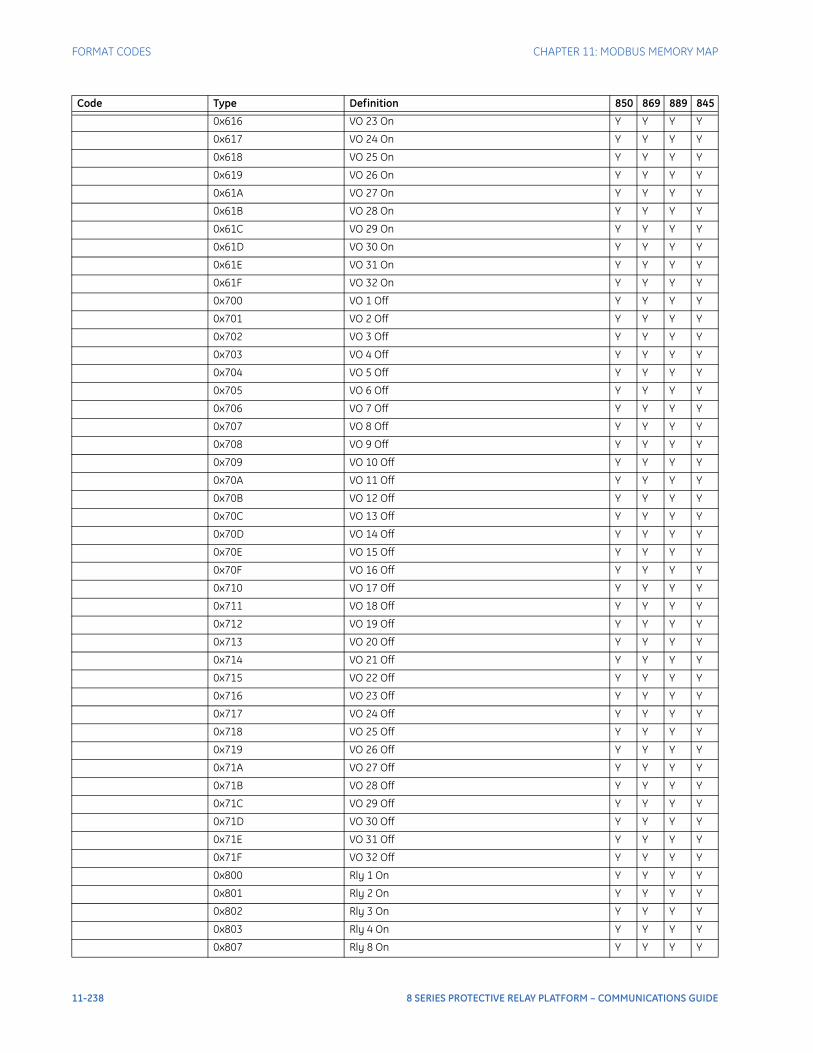
FORMAT CODES CHAPTER 11: MODBUS MEMORY MAP
0x616 VO 23 On Y Y Y Y
0x617 VO 24 On Y Y Y Y
0x618 VO 25 On Y Y Y Y
0x619 VO 26 On Y Y Y Y
0x61A VO 27 On Y Y Y Y
0x61B VO 28 On Y Y Y Y
0x61C VO 29 On Y Y Y Y
0x61D VO 30 On Y Y Y Y
0x61E VO 31 On Y Y Y Y
0x61F VO 32 On Y Y Y Y
0x700 VO 1 Off Y Y Y Y
0x701 VO 2 Off Y Y Y Y
0x702 VO 3 Off Y Y Y Y
0x703 VO 4 Off Y Y Y Y
0x704 VO 5 Off Y Y Y Y
0x705 VO 6 Off Y Y Y Y
0x706 VO 7 Off Y Y Y Y
0x707 VO 8 Off Y Y Y Y
0x708 VO 9 Off Y Y Y Y
0x709 VO 10 Off Y Y Y Y
0x70A VO 11 Off Y Y Y Y
0x70B VO 12 Off Y Y Y Y
0x70C VO 13 Off Y Y Y Y
0x70D VO 14 Off Y Y Y Y
0x70E VO 15 Off Y Y Y Y
0x70F VO 16 Off Y Y Y Y
0x710 VO 17 Off Y Y Y Y
0x711 VO 18 Off Y Y Y Y
0x712 VO 19 Off Y Y Y Y
0x713 VO 20 Off Y Y Y Y
0x714 VO 21 Off Y Y Y Y
0x715 VO 22 Off Y Y Y Y
0x716 VO 23 Off Y Y Y Y
0x717 VO 24 Off Y Y Y Y
0x718 VO 25 Off Y Y Y Y
0x719 VO 26 Off Y Y Y Y
0x71A VO 27 Off Y Y Y Y
0x71B VO 28 Off Y Y Y Y
0x71C VO 29 Off Y Y Y Y
0x71D VO 30 Off Y Y Y Y
0x71E VO 31 Off Y Y Y Y
0x71F VO 32 Off Y Y Y Y
0x800 Rly 1 On Y Y Y Y
0x801 Rly 2 On Y Y Y Y
0x802 Rly 3 On Y Y Y Y
0x803 Rly 4 On Y Y Y Y
0x807 Rly 8 On Y Y Y Y
Code Type Definition 850 869 889 845
11-238 8 SERIES PROTECTIVE RELAY PLATFORM – COMMUNICATIONS GUIDE
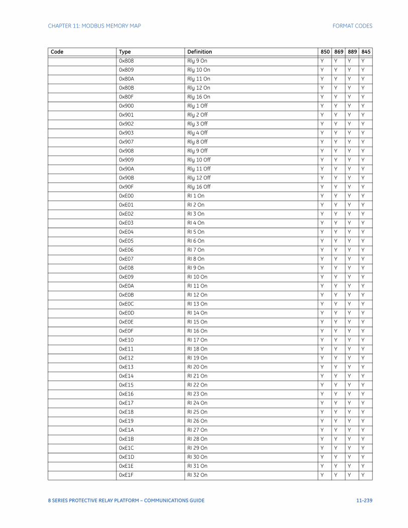
CHAPTER 11: MODBUS MEMORY MAP FORMAT CODES
0x808 Rly 9 On Y Y Y Y
0x809 Rly 10 On Y Y Y Y
0x80A Rly 11 On Y Y Y Y
0x80B Rly 12 On Y Y Y Y
0x80F Rly 16 On Y Y Y Y
0x900 Rly 1 Off Y Y Y Y
0x901 Rly 2 Off Y Y Y Y
0x902 Rly 3 Off Y Y Y Y
0x903 Rly 4 Off Y Y Y Y
0x907 Rly 8 Off Y Y Y Y
0x908 Rly 9 Off Y Y Y Y
0x909 Rly 10 Off Y Y Y Y
0x90A Rly 11 Off Y Y Y Y
0x90B Rly 12 Off Y Y Y Y
0x90F Rly 16 Off Y Y Y Y
0xE00 RI 1 On Y Y Y Y
0xE01 RI 2 On Y Y Y Y
0xE02 RI 3 On Y Y Y Y
0xE03 RI 4 On Y Y Y Y
0xE04 RI 5 On Y Y Y Y
0xE05 RI 6 On Y Y Y Y
0xE06 RI 7 On Y Y Y Y
0xE07 RI 8 On Y Y Y Y
0xE08 RI 9 On Y Y Y Y
0xE09 RI 10 On Y Y Y Y
0xE0A RI 11 On Y Y Y Y
0xE0B RI 12 On Y Y Y Y
0xE0C RI 13 On Y Y Y Y
0xE0D RI 14 On Y Y Y Y
0xE0E RI 15 On Y Y Y Y
0xE0F RI 16 On Y Y Y Y
0xE10 RI 17 On Y Y Y Y
0xE11 RI 18 On Y Y Y Y
0xE12 RI 19 On Y Y Y Y
0xE13 RI 20 On Y Y Y Y
0xE14 RI 21 On Y Y Y Y
0xE15 RI 22 On Y Y Y Y
0xE16 RI 23 On Y Y Y Y
0xE17 RI 24 On Y Y Y Y
0xE18 RI 25 On Y Y Y Y
0xE19 RI 26 On Y Y Y Y
0xE1A RI 27 On Y Y Y Y
0xE1B RI 28 On Y Y Y Y
0xE1C RI 29 On Y Y Y Y
0xE1D RI 30 On Y Y Y Y
0xE1E RI 31 On Y Y Y Y
0xE1F RI 32 On Y Y Y Y
Code Type Definition 850 869 889 845
8 SERIES PROTECTIVE RELAY PLATFORM – COMMUNICATIONS GUIDE 11-239
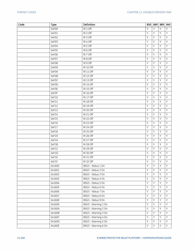
FORMAT CODES CHAPTER 11: MODBUS MEMORY MAP
0xF00 RI 1 Off Y Y Y Y
0xF01 RI 2 Off Y Y Y Y
0xF02 RI 3 Off Y Y Y Y
0xF03 RI 4 Off Y Y Y Y
0xF04 RI 5 Off Y Y Y Y
0xF05 RI 6 Off Y Y Y Y
0xF06 RI 7 Off Y Y Y Y
0xF07 RI 8 Off Y Y Y Y
0xF08 RI 9 Off Y Y Y Y
0xF09 RI 10 Off Y Y Y Y
0xF0A RI 11 Off Y Y Y Y
0xF0B RI 12 Off Y Y Y Y
0xF0C RI 13 Off Y Y Y Y
0xF0D RI 14 Off Y Y Y Y
0xF0E RI 15 Off Y Y Y Y
0xF0F RI 16 Off Y Y Y Y
0xF10 RI 17 Off Y Y Y Y
0xF11 RI 18 Off Y Y Y Y
0xF12 RI 19 Off Y Y Y Y
0xF13 RI 20 Off Y Y Y Y
0xF14 RI 21 Off Y Y Y Y
0xF15 RI 22 Off Y Y Y Y
0xF16 RI 23 Off Y Y Y Y
0xF17 RI 24 Off Y Y Y Y
0xF18 RI 25 Off Y Y Y Y
0xF19 RI 26 Off Y Y Y Y
0xF1A RI 27 Off Y Y Y Y
0xF1B RI 28 Off Y Y Y Y
0xF1C RI 29 Off Y Y Y Y
0xF1D RI 30 Off Y Y Y Y
0xF1E RI 31 Off Y Y Y Y
0xF1F RI 32 Off Y Y Y Y
0x1600 BSG3 - Status 1 On Y Y Y Y
0x1601 BSG3 - Status 2 On Y Y Y Y
0x1602 BSG3 - Status 3 On Y Y Y Y
0x1603 BSG3 - Status 4 On Y Y Y Y
0x1604 BSG3 - Status 5 On Y Y Y Y
0x1605 BSG3 - Status 6 On Y Y Y Y
0x1606 BSG3 - Status 7 On Y Y Y Y
0x1607 BSG3 - Status 8 On Y Y Y Y
0x1608 BSG3 - Status 9 On Y Y Y Y
0x1609 BSG3 - Warning 1 On Y Y Y Y
0x160A BSG3 - Warning 2 On Y Y Y Y
0x160B BSG3 - Warning 3 On Y Y Y Y
0x160C BSG3 - Warning 4 On Y Y Y Y
0x160D BSG3 - Warning 5 On Y Y Y Y
0x160E BSG3 - Warning 6 On Y Y Y Y
Code Type Definition 850 869 889 845
11-240 8 SERIES PROTECTIVE RELAY PLATFORM – COMMUNICATIONS GUIDE
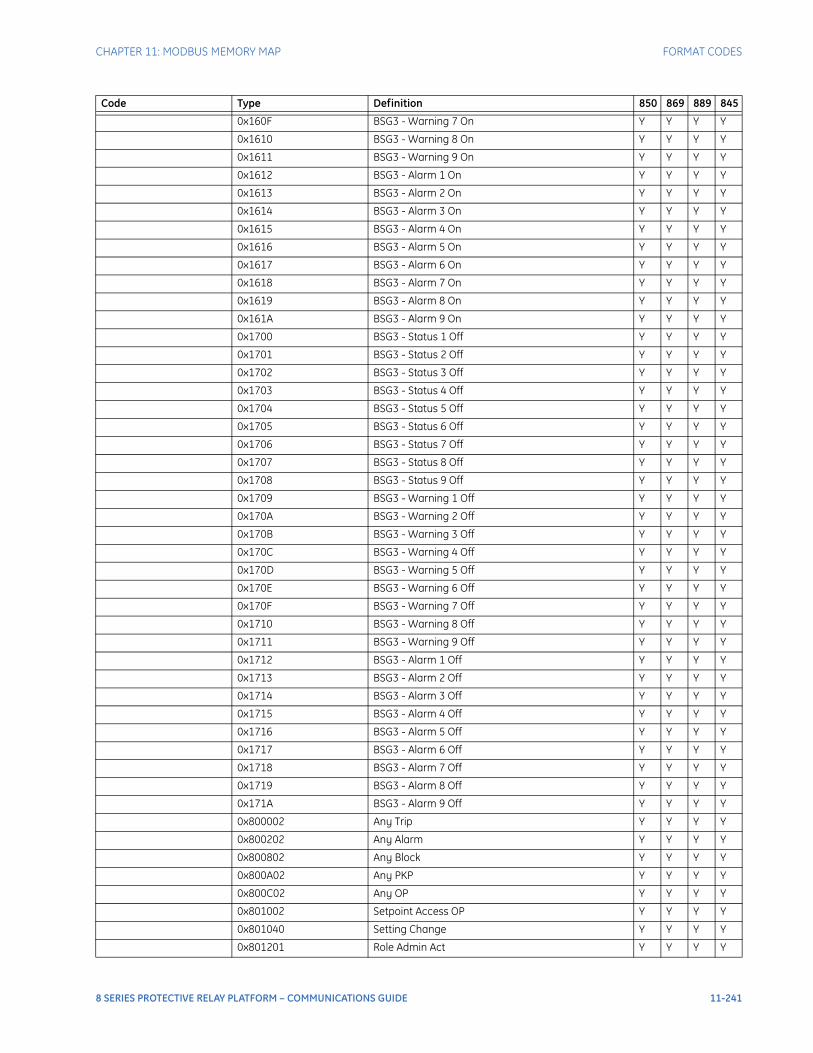
CHAPTER 11: MODBUS MEMORY MAP FORMAT CODES
0x160F BSG3 - Warning 7 On Y Y Y Y
0x1610 BSG3 - Warning 8 On Y Y Y Y
0x1611 BSG3 - Warning 9 On Y Y Y Y
0x1612 BSG3 - Alarm 1 On Y Y Y Y
0x1613 BSG3 - Alarm 2 On Y Y Y Y
0x1614 BSG3 - Alarm 3 On Y Y Y Y
0x1615 BSG3 - Alarm 4 On Y Y Y Y
0x1616 BSG3 - Alarm 5 On Y Y Y Y
0x1617 BSG3 - Alarm 6 On Y Y Y Y
0x1618 BSG3 - Alarm 7 On Y Y Y Y
0x1619 BSG3 - Alarm 8 On Y Y Y Y
0x161A BSG3 - Alarm 9 On Y Y Y Y
0x1700 BSG3 - Status 1 Off Y Y Y Y
0x1701 BSG3 - Status 2 Off Y Y Y Y
0x1702 BSG3 - Status 3 Off Y Y Y Y
0x1703 BSG3 - Status 4 Off Y Y Y Y
0x1704 BSG3 - Status 5 Off Y Y Y Y
0x1705 BSG3 - Status 6 Off Y Y Y Y
0x1706 BSG3 - Status 7 Off Y Y Y Y
0x1707 BSG3 - Status 8 Off Y Y Y Y
0x1708 BSG3 - Status 9 Off Y Y Y Y
0x1709 BSG3 - Warning 1 Off Y Y Y Y
0x170A BSG3 - Warning 2 Off Y Y Y Y
0x170B BSG3 - Warning 3 Off Y Y Y Y
0x170C BSG3 - Warning 4 Off Y Y Y Y
0x170D BSG3 - Warning 5 Off Y Y Y Y
0x170E BSG3 - Warning 6 Off Y Y Y Y
0x170F BSG3 - Warning 7 Off Y Y Y Y
0x1710 BSG3 - Warning 8 Off Y Y Y Y
0x1711 BSG3 - Warning 9 Off Y Y Y Y
0x1712 BSG3 - Alarm 1 Off Y Y Y Y
0x1713 BSG3 - Alarm 2 Off Y Y Y Y
0x1714 BSG3 - Alarm 3 Off Y Y Y Y
0x1715 BSG3 - Alarm 4 Off Y Y Y Y
0x1716 BSG3 - Alarm 5 Off Y Y Y Y
0x1717 BSG3 - Alarm 6 Off Y Y Y Y
0x1718 BSG3 - Alarm 7 Off Y Y Y Y
0x1719 BSG3 - Alarm 8 Off Y Y Y Y
0x171A BSG3 - Alarm 9 Off Y Y Y Y
0x800002 Any Trip Y Y Y Y
0x800202 Any Alarm Y Y Y Y
0x800802 Any Block Y Y Y Y
0x800A02 Any PKP Y Y Y Y
0x800C02 Any OP Y Y Y Y
0x801002 Setpoint Access OP Y Y Y Y
0x801040 Setting Change Y Y Y Y
0x801201 Role Admin Act Y Y Y Y
Code Type Definition 850 869 889 845
8 SERIES PROTECTIVE RELAY PLATFORM – COMMUNICATIONS GUIDE 11-241
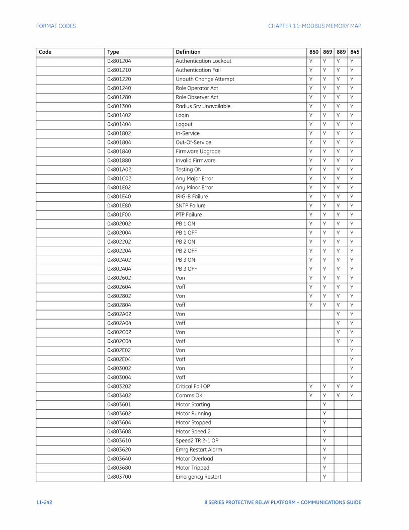
FORMAT CODES CHAPTER 11: MODBUS MEMORY MAP
0x801204 Authentication Lockout Y Y Y Y
0x801210 Authentication Fail Y Y Y Y
0x801220 Unauth Change Attempt Y Y Y Y
0x801240 Role Operator Act Y Y Y Y
0x801280 Role Observer Act Y Y Y Y
0x801300 Radius Srv Unavailable Y Y Y Y
0x801402 Login Y Y Y Y
0x801404 Logout Y Y Y Y
0x801802 In-Service Y Y Y Y
0x801804 Out-Of-Service Y Y Y Y
0x801840 Firmware Upgrade Y Y Y Y
0x801880 Invalid Firmware Y Y Y Y
0x801A02 Testing ON Y Y Y Y
0x801C02 Any Major Error Y Y Y Y
0x801E02 Any Minor Error Y Y Y Y
0x801E40 IRIG-B Failure Y Y Y Y
0x801E80 SNTP Failure Y Y Y Y
0x801F00 PTP Failure Y Y Y Y
0x802002 PB 1 ON Y Y Y Y
0x802004 PB 1 OFF Y Y Y Y
0x802202 PB 2 ON Y Y Y Y
0x802204 PB 2 OFF Y Y Y Y
0x802402 PB 3 ON Y Y Y Y
0x802404 PB 3 OFF Y Y Y Y
0x802602 Von Y Y Y Y
0x802604 Voff Y Y Y Y
0x802802 Von Y Y Y Y
0x802804 Voff Y Y Y Y
0x802A02 Von Y Y
0x802A04 Voff Y Y
0x802C02 Von Y Y
0x802C04 Voff Y Y
0x802E02 Von Y
0x802E04 Voff Y
0x803002 Von Y
0x803004 Voff Y
0x803202 Critical Fail OP Y Y Y Y
0x803402 Comms OK Y Y Y Y
0x803601 Motor Starting Y
0x803602 Motor Running Y
0x803604 Motor Stopped Y
0x803608 Motor Speed 2 Y
0x803610 Speed2 TR 2-1 OP Y
0x803620 Emrg Restart Alarm Y
0x803640 Motor Overload Y
0x803680 Motor Tripped Y
0x803700 Emergency Restart Y
Code Type Definition 850 869 889 845
11-242 8 SERIES PROTECTIVE RELAY PLATFORM – COMMUNICATIONS GUIDE
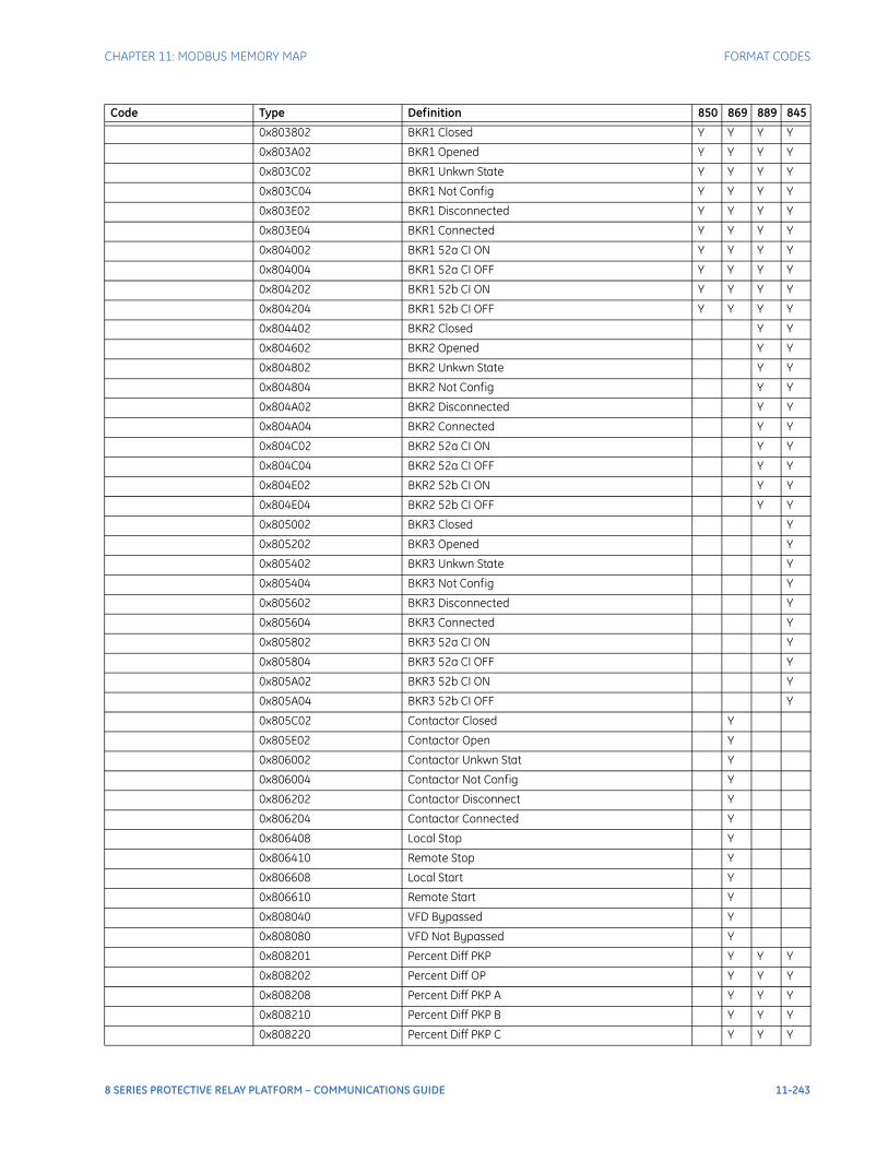
CHAPTER 11: MODBUS MEMORY MAP FORMAT CODES
0x803802 BKR1 Closed Y Y Y Y
0x803A02 BKR1 Opened Y Y Y Y
0x803C02 BKR1 Unkwn State Y Y Y Y
0x803C04 BKR1 Not Config Y Y Y Y
0x803E02 BKR1 Disconnected Y Y Y Y
0x803E04 BKR1 Connected Y Y Y Y
0x804002 BKR1 52a CI ON Y Y Y Y
0x804004 BKR1 52a CI OFF Y Y Y Y
0x804202 BKR1 52b CI ON Y Y Y Y
0x804204 BKR1 52b CI OFF Y Y Y Y
0x804402 BKR2 Closed Y Y
0x804602 BKR2 Opened Y Y
0x804802 BKR2 Unkwn State Y Y
0x804804 BKR2 Not Config Y Y
0x804A02 BKR2 Disconnected Y Y
0x804A04 BKR2 Connected Y Y
0x804C02 BKR2 52a CI ON Y Y
0x804C04 BKR2 52a CI OFF Y Y
0x804E02 BKR2 52b CI ON Y Y
0x804E04 BKR2 52b CI OFF Y Y
0x805002 BKR3 Closed Y
0x805202 BKR3 Opened Y
0x805402 BKR3 Unkwn State Y
0x805404 BKR3 Not Config Y
0x805602 BKR3 Disconnected Y
0x805604 BKR3 Connected Y
0x805802 BKR3 52a CI ON Y
0x805804 BKR3 52a CI OFF Y
0x805A02 BKR3 52b CI ON Y
0x805A04 BKR3 52b CI OFF Y
0x805C02 Contactor Closed Y
0x805E02 Contactor Open Y
0x806002 Contactor Unkwn Stat Y
0x806004 Contactor Not Config Y
0x806202 Contactor Disconnect Y
0x806204 Contactor Connected Y
0x806408 Local Stop Y
0x806410 Remote Stop Y
0x806608 Local Start Y
0x806610 Remote Start Y
0x808040 VFD Bypassed Y
0x808080 VFD Not Bypassed Y
0x808201 Percent Diff PKP Y Y Y
0x808202 Percent Diff OP Y Y Y
0x808208 Percent Diff PKP A Y Y Y
0x808210 Percent Diff PKP B Y Y Y
0x808220 Percent Diff PKP C Y Y Y
Code Type Definition 850 869 889 845
8 SERIES PROTECTIVE RELAY PLATFORM – COMMUNICATIONS GUIDE 11-243
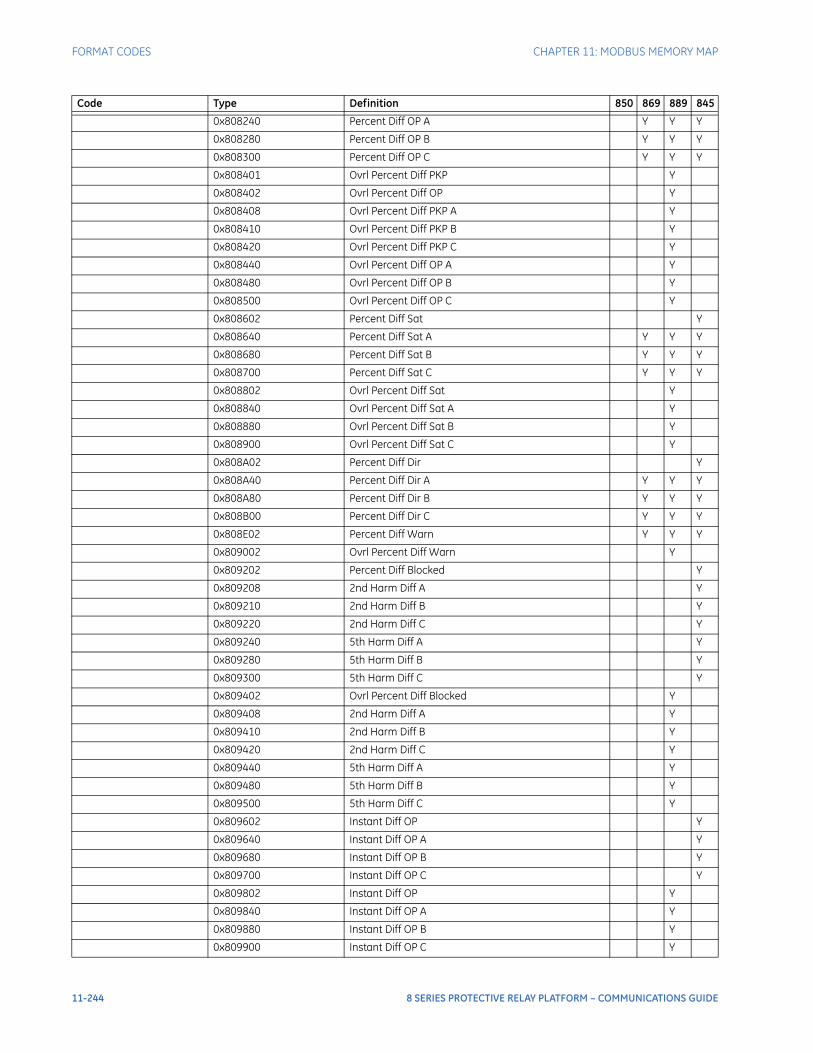
FORMAT CODES CHAPTER 11: MODBUS MEMORY MAP
0x808240 Percent Diff OP A Y Y Y
0x808280 Percent Diff OP B Y Y Y
0x808300 Percent Diff OP C Y Y Y
0x808401 Ovrl Percent Diff PKP Y
0x808402 Ovrl Percent Diff OP Y
0x808408 Ovrl Percent Diff PKP A Y
0x808410 Ovrl Percent Diff PKP B Y
0x808420 Ovrl Percent Diff PKP C Y
0x808440 Ovrl Percent Diff OP A Y
0x808480 Ovrl Percent Diff OP B Y
0x808500 Ovrl Percent Diff OP C Y
0x808602 Percent Diff Sat Y
0x808640 Percent Diff Sat A Y Y Y
0x808680 Percent Diff Sat B Y Y Y
0x808700 Percent Diff Sat C Y Y Y
0x808802 Ovrl Percent Diff Sat Y
0x808840 Ovrl Percent Diff Sat A Y
0x808880 Ovrl Percent Diff Sat B Y
0x808900 Ovrl Percent Diff Sat C Y
0x808A02 Percent Diff Dir Y
0x808A40 Percent Diff Dir A Y Y Y
0x808A80 Percent Diff Dir B Y Y Y
0x808B00 Percent Diff Dir C Y Y Y
0x808E02 Percent Diff Warn Y Y Y
0x809002 Ovrl Percent Diff Warn Y
0x809202 Percent Diff Blocked Y
0x809208 2nd Harm Diff A Y
0x809210 2nd Harm Diff B Y
0x809220 2nd Harm Diff C Y
0x809240 5th Harm Diff A Y
0x809280 5th Harm Diff B Y
0x809300 5th Harm Diff C Y
0x809402 Ovrl Percent Diff Blocked Y
0x809408 2nd Harm Diff A Y
0x809410 2nd Harm Diff B Y
0x809420 2nd Harm Diff C Y
0x809440 5th Harm Diff A Y
0x809480 5th Harm Diff B Y
0x809500 5th Harm Diff C Y
0x809602 Instant Diff OP Y
0x809640 Instant Diff OP A Y
0x809680 Instant Diff OP B Y
0x809700 Instant Diff OP C Y
0x809802 Instant Diff OP Y
0x809840 Instant Diff OP A Y
0x809880 Instant Diff OP B Y
0x809900 Instant Diff OP C Y
Code Type Definition 850 869 889 845
11-244 8 SERIES PROTECTIVE RELAY PLATFORM – COMMUNICATIONS GUIDE
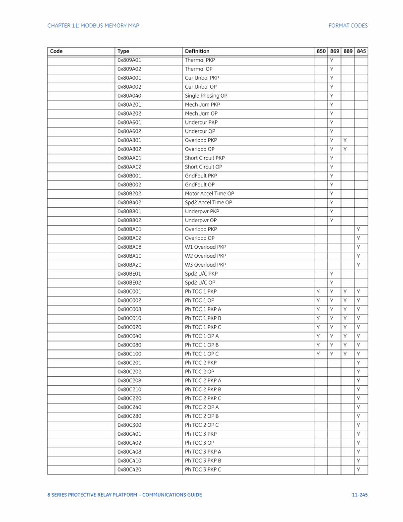
CHAPTER 11: MODBUS MEMORY MAP FORMAT CODES
0x809A01 Thermal PKP Y
0x809A02 Thermal OP Y
0x80A001 Cur Unbal PKP Y
0x80A002 Cur Unbal OP Y
0x80A040 Single Phasing OP Y
0x80A201 Mech Jam PKP Y
0x80A202 Mech Jam OP Y
0x80A601 Undercur PKP Y
0x80A602 Undercur OP Y
0x80A801 Overload PKP Y Y
0x80A802 Overload OP Y Y
0x80AA01 Short Circuit PKP Y
0x80AA02 Short Circuit OP Y
0x80B001 GndFault PKP Y
0x80B002 GndFault OP Y
0x80B202 Motor Accel Time OP Y
0x80B402 Spd2 Accel Time OP Y
0x80B801 Underpwr PKP Y
0x80B802 Underpwr OP Y
0x80BA01 Overload PKP Y
0x80BA02 Overload OP Y
0x80BA08 W1 Overload PKP Y
0x80BA10 W2 Overload PKP Y
0x80BA20 W3 Overload PKP Y
0x80BE01 Spd2 U/C PKP Y
0x80BE02 Spd2 U/C OP Y
0x80C001 Ph TOC 1 PKP Y Y Y Y
0x80C002 Ph TOC 1 OP Y Y Y Y
0x80C008 Ph TOC 1 PKP A Y Y Y Y
0x80C010 Ph TOC 1 PKP B Y Y Y Y
0x80C020 Ph TOC 1 PKP C Y Y Y Y
0x80C040 Ph TOC 1 OP A Y Y Y Y
0x80C080 Ph TOC 1 OP B Y Y Y Y
0x80C100 Ph TOC 1 OP C Y Y Y Y
0x80C201 Ph TOC 2 PKP Y
0x80C202 Ph TOC 2 OP Y
0x80C208 Ph TOC 2 PKP A Y
0x80C210 Ph TOC 2 PKP B Y
0x80C220 Ph TOC 2 PKP C Y
0x80C240 Ph TOC 2 OP A Y
0x80C280 Ph TOC 2 OP B Y
0x80C300 Ph TOC 2 OP C Y
0x80C401 Ph TOC 3 PKP Y
0x80C402 Ph TOC 3 OP Y
0x80C408 Ph TOC 3 PKP A Y
0x80C410 Ph TOC 3 PKP B Y
0x80C420 Ph TOC 3 PKP C Y
Code Type Definition 850 869 889 845
8 SERIES PROTECTIVE RELAY PLATFORM – COMMUNICATIONS GUIDE 11-245
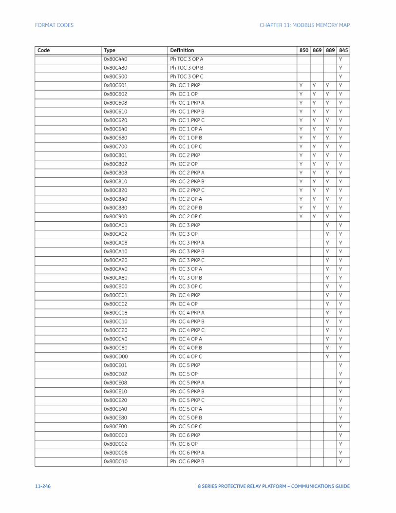
FORMAT CODES CHAPTER 11: MODBUS MEMORY MAP
0x80C440 Ph TOC 3 OP A Y
0x80C480 Ph TOC 3 OP B Y
0x80C500 Ph TOC 3 OP C Y
0x80C601 Ph IOC 1 PKP Y Y Y Y
0x80C602 Ph IOC 1 OP Y Y Y Y
0x80C608 Ph IOC 1 PKP A Y Y Y Y
0x80C610 Ph IOC 1 PKP B Y Y Y Y
0x80C620 Ph IOC 1 PKP C Y Y Y Y
0x80C640 Ph IOC 1 OP A Y Y Y Y
0x80C680 Ph IOC 1 OP B Y Y Y Y
0x80C700 Ph IOC 1 OP C Y Y Y Y
0x80C801 Ph IOC 2 PKP Y Y Y Y
0x80C802 Ph IOC 2 OP Y Y Y Y
0x80C808 Ph IOC 2 PKP A Y Y Y Y
0x80C810 Ph IOC 2 PKP B Y Y Y Y
0x80C820 Ph IOC 2 PKP C Y Y Y Y
0x80C840 Ph IOC 2 OP A Y Y Y Y
0x80C880 Ph IOC 2 OP B Y Y Y Y
0x80C900 Ph IOC 2 OP C Y Y Y Y
0x80CA01 Ph IOC 3 PKP Y Y
0x80CA02 Ph IOC 3 OP Y Y
0x80CA08 Ph IOC 3 PKP A Y Y
0x80CA10 Ph IOC 3 PKP B Y Y
0x80CA20 Ph IOC 3 PKP C Y Y
0x80CA40 Ph IOC 3 OP A Y Y
0x80CA80 Ph IOC 3 OP B Y Y
0x80CB00 Ph IOC 3 OP C Y Y
0x80CC01 Ph IOC 4 PKP Y Y
0x80CC02 Ph IOC 4 OP Y Y
0x80CC08 Ph IOC 4 PKP A Y Y
0x80CC10 Ph IOC 4 PKP B Y Y
0x80CC20 Ph IOC 4 PKP C Y Y
0x80CC40 Ph IOC 4 OP A Y Y
0x80CC80 Ph IOC 4 OP B Y Y
0x80CD00 Ph IOC 4 OP C Y Y
0x80CE01 Ph IOC 5 PKP Y
0x80CE02 Ph IOC 5 OP Y
0x80CE08 Ph IOC 5 PKP A Y
0x80CE10 Ph IOC 5 PKP B Y
0x80CE20 Ph IOC 5 PKP C Y
0x80CE40 Ph IOC 5 OP A Y
0x80CE80 Ph IOC 5 OP B Y
0x80CF00 Ph IOC 5 OP C Y
0x80D001 Ph IOC 6 PKP Y
0x80D002 Ph IOC 6 OP Y
0x80D008 Ph IOC 6 PKP A Y
0x80D010 Ph IOC 6 PKP B Y
Code Type Definition 850 869 889 845
11-246 8 SERIES PROTECTIVE RELAY PLATFORM – COMMUNICATIONS GUIDE
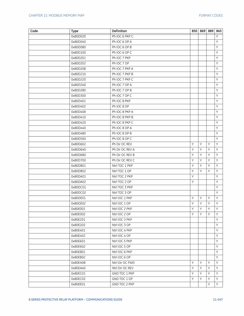
CHAPTER 11: MODBUS MEMORY MAP FORMAT CODES
0x80D020 Ph IOC 6 PKP C Y
0x80D040 Ph IOC 6 OP A Y
0x80D080 Ph IOC 6 OP B Y
0x80D100 Ph IOC 6 OP C Y
0x80D201 Ph IOC 7 PKP Y
0x80D202 Ph IOC 7 OP Y
0x80D208 Ph IOC 7 PKP A Y
0x80D210 Ph IOC 7 PKP B Y
0x80D220 Ph IOC 7 PKP C Y
0x80D240 Ph IOC 7 OP A Y
0x80D280 Ph IOC 7 OP B Y
0x80D300 Ph IOC 7 OP C Y
0x80D401 Ph IOC 8 PKP Y
0x80D402 Ph IOC 8 OP Y
0x80D408 Ph IOC 8 PKP A Y
0x80D410 Ph IOC 8 PKP B Y
0x80D420 Ph IOC 8 PKP C Y
0x80D440 Ph IOC 8 OP A Y
0x80D480 Ph IOC 8 OP B Y
0x80D500 Ph IOC 8 OP C Y
0x80D602 Ph Dir OC REV Y Y Y Y
0x80D640 Ph Dir OC REV A Y Y Y Y
0x80D680 Ph Dir OC REV B Y Y Y Y
0x80D700 Ph Dir OC REV C Y Y Y Y
0x80D801 Ntrl TOC 1 PKP Y Y Y Y
0x80D802 Ntrl TOC 1 OP Y Y Y Y
0x80DA01 Ntrl TOC 2 PKP Y Y
0x80DA02 Ntrl TOC 2 OP Y Y
0x80DC01 Ntrl TOC 3 PKP Y
0x80DC02 Ntrl TOC 3 OP Y
0x80DE01 Ntrl IOC 1 PKP Y Y Y Y
0x80DE02 Ntrl IOC 1 OP Y Y Y Y
0x80E001 Ntrl IOC 2 PKP Y Y Y Y
0x80E002 Ntrl IOC 2 OP Y Y Y Y
0x80E201 Ntrl IOC 3 PKP Y
0x80E202 Ntrl IOC 3 OP Y
0x80E401 Ntrl IOC 4 PKP Y
0x80E402 Ntrl IOC 4 OP Y
0x80E601 Ntrl IOC 5 PKP Y
0x80E602 Ntrl IOC 5 OP Y
0x80E801 Ntrl IOC 6 PKP Y
0x80E802 Ntrl IOC 6 OP Y
0x80EA08 Ntrl Dir OC FWD Y Y Y Y
0x80EA40 Ntrl Dir OC REV Y Y Y Y
0x80EC01 GND TOC 1 PKP Y Y Y Y
0x80EC02 GND TOC 1 OP Y Y Y Y
0x80EE01 GND TOC 2 PKP Y Y
Code Type Definition 850 869 889 845
8 SERIES PROTECTIVE RELAY PLATFORM – COMMUNICATIONS GUIDE 11-247
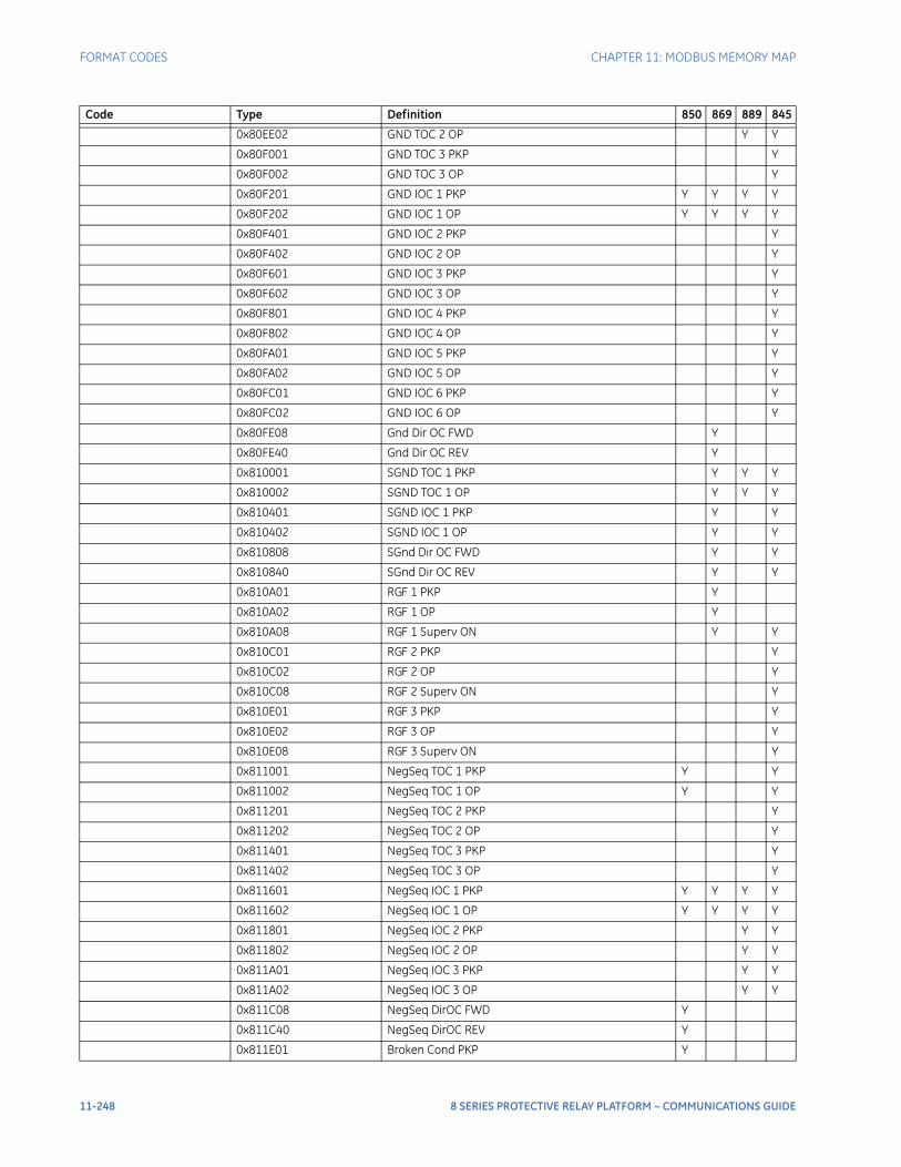
FORMAT CODES CHAPTER 11: MODBUS MEMORY MAP
0x80EE02 GND TOC 2 OP Y Y
0x80F001 GND TOC 3 PKP Y
0x80F002 GND TOC 3 OP Y
0x80F201 GND IOC 1 PKP Y Y Y Y
0x80F202 GND IOC 1 OP Y Y Y Y
0x80F401 GND IOC 2 PKP Y
0x80F402 GND IOC 2 OP Y
0x80F601 GND IOC 3 PKP Y
0x80F602 GND IOC 3 OP Y
0x80F801 GND IOC 4 PKP Y
0x80F802 GND IOC 4 OP Y
0x80FA01 GND IOC 5 PKP Y
0x80FA02 GND IOC 5 OP Y
0x80FC01 GND IOC 6 PKP Y
0x80FC02 GND IOC 6 OP Y
0x80FE08 Gnd Dir OC FWD Y
0x80FE40 Gnd Dir OC REV Y
0x810001 SGND TOC 1 PKP Y Y Y
0x810002 SGND TOC 1 OP Y Y Y
0x810401 SGND IOC 1 PKP Y Y
0x810402 SGND IOC 1 OP Y Y
0x810808 SGnd Dir OC FWD Y Y
0x810840 SGnd Dir OC REV Y Y
0x810A01 RGF 1 PKP Y
0x810A02 RGF 1 OP Y
0x810A08 RGF 1 Superv ON Y Y
0x810C01 RGF 2 PKP Y
0x810C02 RGF 2 OP Y
0x810C08 RGF 2 Superv ON Y
0x810E01 RGF 3 PKP Y
0x810E02 RGF 3 OP Y
0x810E08 RGF 3 Superv ON Y
0x811001 NegSeq TOC 1 PKP Y Y
0x811002 NegSeq TOC 1 OP Y Y
0x811201 NegSeq TOC 2 PKP Y
0x811202 NegSeq TOC 2 OP Y
0x811401 NegSeq TOC 3 PKP Y
0x811402 NegSeq TOC 3 OP Y
0x811601 NegSeq IOC 1 PKP Y Y Y Y
0x811602 NegSeq IOC 1 OP Y Y Y Y
0x811801 NegSeq IOC 2 PKP Y Y
0x811802 NegSeq IOC 2 OP Y Y
0x811A01 NegSeq IOC 3 PKP Y Y
0x811A02 NegSeq IOC 3 OP Y Y
0x811C08 NegSeq DirOC FWD Y
0x811C40 NegSeq DirOC REV Y
0x811E01 Broken Cond PKP Y
Code Type Definition 850 869 889 845
11-248 8 SERIES PROTECTIVE RELAY PLATFORM – COMMUNICATIONS GUIDE
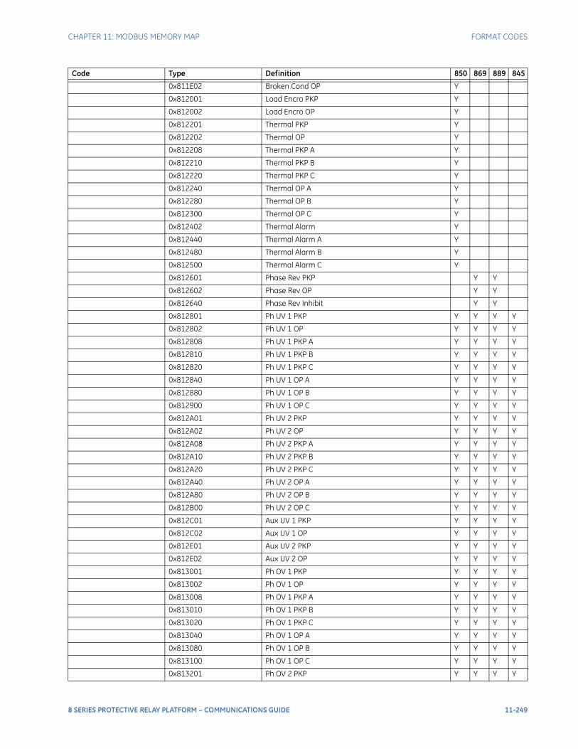
CHAPTER 11: MODBUS MEMORY MAP FORMAT CODES
0x811E02 Broken Cond OP Y
0x812001 Load Encro PKP Y
0x812002 Load Encro OP Y
0x812201 Thermal PKP Y
0x812202 Thermal OP Y
0x812208 Thermal PKP A Y
0x812210 Thermal PKP B Y
0x812220 Thermal PKP C Y
0x812240 Thermal OP A Y
0x812280 Thermal OP B Y
0x812300 Thermal OP C Y
0x812402 Thermal Alarm Y
0x812440 Thermal Alarm A Y
0x812480 Thermal Alarm B Y
0x812500 Thermal Alarm C Y
0x812601 Phase Rev PKP Y Y
0x812602 Phase Rev OP Y Y
0x812640 Phase Rev Inhibit Y Y
0x812801 Ph UV 1 PKP Y Y Y Y
0x812802 Ph UV 1 OP Y Y Y Y
0x812808 Ph UV 1 PKP A Y Y Y Y
0x812810 Ph UV 1 PKP B Y Y Y Y
0x812820 Ph UV 1 PKP C Y Y Y Y
0x812840 Ph UV 1 OP A Y Y Y Y
0x812880 Ph UV 1 OP B Y Y Y Y
0x812900 Ph UV 1 OP C Y Y Y Y
0x812A01 Ph UV 2 PKP Y Y Y Y
0x812A02 Ph UV 2 OP Y Y Y Y
0x812A08 Ph UV 2 PKP A Y Y Y Y
0x812A10 Ph UV 2 PKP B Y Y Y Y
0x812A20 Ph UV 2 PKP C Y Y Y Y
0x812A40 Ph UV 2 OP A Y Y Y Y
0x812A80 Ph UV 2 OP B Y Y Y Y
0x812B00 Ph UV 2 OP C Y Y Y Y
0x812C01 Aux UV 1 PKP Y Y Y Y
0x812C02 Aux UV 1 OP Y Y Y Y
0x812E01 Aux UV 2 PKP Y Y Y Y
0x812E02 Aux UV 2 OP Y Y Y Y
0x813001 Ph OV 1 PKP Y Y Y Y
0x813002 Ph OV 1 OP Y Y Y Y
0x813008 Ph OV 1 PKP A Y Y Y Y
0x813010 Ph OV 1 PKP B Y Y Y Y
0x813020 Ph OV 1 PKP C Y Y Y Y
0x813040 Ph OV 1 OP A Y Y Y Y
0x813080 Ph OV 1 OP B Y Y Y Y
0x813100 Ph OV 1 OP C Y Y Y Y
0x813201 Ph OV 2 PKP Y Y Y Y
Code Type Definition 850 869 889 845
8 SERIES PROTECTIVE RELAY PLATFORM – COMMUNICATIONS GUIDE 11-249
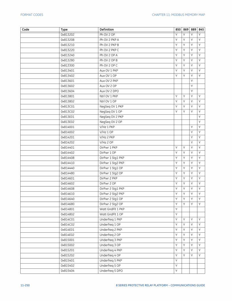
FORMAT CODES CHAPTER 11: MODBUS MEMORY MAP
0x813202 Ph OV 2 OP Y Y Y Y
0x813208 Ph OV 2 PKP A Y Y Y Y
0x813210 Ph OV 2 PKP B Y Y Y Y
0x813220 Ph OV 2 PKP C Y Y Y Y
0x813240 Ph OV 2 OP A Y Y Y Y
0x813280 Ph OV 2 OP B Y Y Y Y
0x813300 Ph OV 2 OP C Y Y Y Y
0x813401 Aux OV 1 PKP Y Y Y Y
0x813402 Aux OV 1 OP Y Y Y Y
0x813601 Aux OV 2 PKP Y
0x813602 Aux OV 2 OP Y
0x813604 Aux OV 2 DPO Y
0x813801 Ntrl OV 1 PKP Y Y Y Y
0x813802 Ntrl OV 1 OP Y Y Y Y
0x813C01 NegSeq OV 1 PKP Y Y Y Y
0x813C02 NegSeq OV 1 OP Y Y Y Y
0x813E01 NegSeq OV 2 PKP Y
0x813E02 NegSeq OV 2 OP Y
0x814001 V/Hz 1 PKP Y Y
0x814002 V/Hz 1 OP Y Y
0x814201 V/Hz 2 PKP Y Y
0x814202 V/Hz 2 OP Y Y
0x814401 DirPwr 1 PKP Y Y Y Y
0x814402 DirPwr 1 OP Y Y Y Y
0x814408 DirPwr 1 Stg1 PKP Y Y Y Y
0x814410 DirPwr 1 Stg2 PKP Y Y Y Y
0x814440 DirPwr 1 Stg1 OP Y Y Y Y
0x814480 DirPwr 1 Stg2 OP Y Y Y Y
0x814601 DirPwr 2 PKP Y Y Y Y
0x814602 DirPwr 2 OP Y Y Y Y
0x814608 DirPwr 2 Stg1 PKP Y Y Y Y
0x814610 DirPwr 2 Stg2 PKP Y Y Y Y
0x814640 DirPwr 2 Stg1 OP Y Y Y Y
0x814680 DirPwr 2 Stg2 OP Y Y Y Y
0x814801 Watt GndFlt 1 PKP Y
0x814802 Watt GndFlt 1 OP Y
0x814C01 Underfreq 1 PKP Y Y Y Y
0x814C02 Underfreq 1 OP Y Y Y Y
0x814E01 Underfreq 2 PKP Y Y Y Y
0x814E02 Underfreq 2 OP Y Y Y Y
0x815001 Underfreq 3 PKP Y Y Y Y
0x815002 Underfreq 3 OP Y Y Y Y
0x815201 Underfreq 4 PKP Y Y Y Y
0x815202 Underfreq 4 OP Y Y Y Y
0x815401 Underfreq 5 PKP Y
0x815402 Underfreq 5 OP Y
0x815404 Underfreq 5 DPO Y
Code Type Definition 850 869 889 845
11-250 8 SERIES PROTECTIVE RELAY PLATFORM – COMMUNICATIONS GUIDE
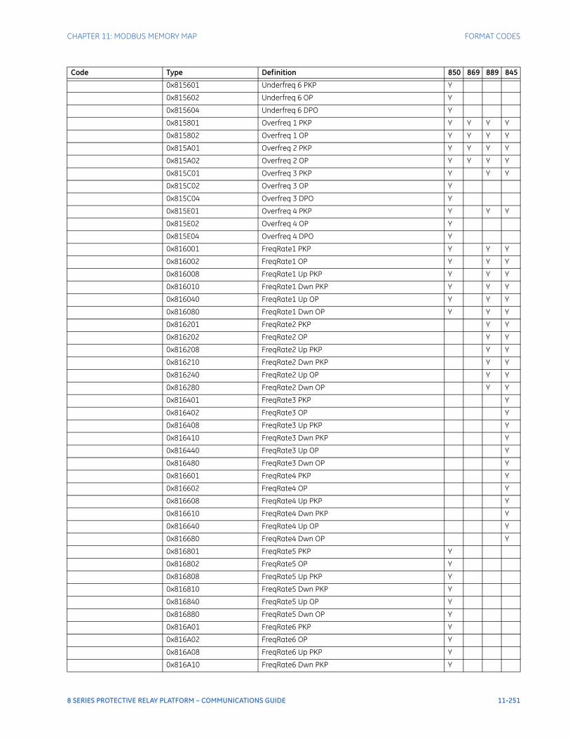
CHAPTER 11: MODBUS MEMORY MAP FORMAT CODES
0x815601 Underfreq 6 PKP Y
0x815602 Underfreq 6 OP Y
0x815604 Underfreq 6 DPO Y
0x815801 Overfreq 1 PKP Y Y Y Y
0x815802 Overfreq 1 OP Y Y Y Y
0x815A01 Overfreq 2 PKP Y Y Y Y
0x815A02 Overfreq 2 OP Y Y Y Y
0x815C01 Overfreq 3 PKP Y Y Y
0x815C02 Overfreq 3 OP Y
0x815C04 Overfreq 3 DPO Y
0x815E01 Overfreq 4 PKP Y Y Y
0x815E02 Overfreq 4 OP Y
0x815E04 Overfreq 4 DPO Y
0x816001 FreqRate1 PKP Y Y Y
0x816002 FreqRate1 OP Y Y Y
0x816008 FreqRate1 Up PKP Y Y Y
0x816010 FreqRate1 Dwn PKP Y Y Y
0x816040 FreqRate1 Up OP Y Y Y
0x816080 FreqRate1 Dwn OP Y Y Y
0x816201 FreqRate2 PKP Y Y
0x816202 FreqRate2 OP Y Y
0x816208 FreqRate2 Up PKP Y Y
0x816210 FreqRate2 Dwn PKP Y Y
0x816240 FreqRate2 Up OP Y Y
0x816280 FreqRate2 Dwn OP Y Y
0x816401 FreqRate3 PKP Y
0x816402 FreqRate3 OP Y
0x816408 FreqRate3 Up PKP Y
0x816410 FreqRate3 Dwn PKP Y
0x816440 FreqRate3 Up OP Y
0x816480 FreqRate3 Dwn OP Y
0x816601 FreqRate4 PKP Y
0x816602 FreqRate4 OP Y
0x816608 FreqRate4 Up PKP Y
0x816610 FreqRate4 Dwn PKP Y
0x816640 FreqRate4 Up OP Y
0x816680 FreqRate4 Dwn OP Y
0x816801 FreqRate5 PKP Y
0x816802 FreqRate5 OP Y
0x816808 FreqRate5 Up PKP Y
0x816810 FreqRate5 Dwn PKP Y
0x816840 FreqRate5 Up OP Y
0x816880 FreqRate5 Dwn OP Y
0x816A01 FreqRate6 PKP Y
0x816A02 FreqRate6 OP Y
0x816A08 FreqRate6 Up PKP Y
0x816A10 FreqRate6 Dwn PKP Y
Code Type Definition 850 869 889 845
8 SERIES PROTECTIVE RELAY PLATFORM – COMMUNICATIONS GUIDE 11-251
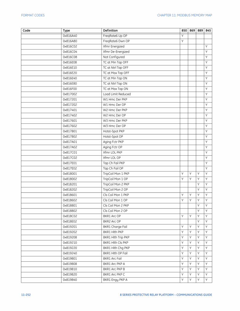
FORMAT CODES CHAPTER 11: MODBUS MEMORY MAP
0x816A40 FreqRate6 Up OP Y
0x816A80 FreqRate6 Dwn OP Y
0x816C02 Xfmr Energized Y
0x816C04 Xfmr De-Energized Y
0x816C08 Not Configured Y
0x816E08 TC at Min Tap OFF Y
0x816E10 TC at Ntrl Tap OFF Y
0x816E20 TC at Max Tap OFF Y
0x816E40 TC at Min Tap ON Y
0x816E80 TC at Ntrl Tap ON Y
0x816F00 TC at Max Tap ON Y
0x817002 Load Limit Reduced Y
0x817201 W1 Hmc Der PKP Y
0x817202 W1 Hmc Der OP Y
0x817401 W2 Hmc Der PKP Y
0x817402 W2 Hmc Der OP Y
0x817601 W3 Hmc Der PKP Y
0x817602 W3 Hmc Der OP Y
0x817801 Hotst-Spot PKP Y
0x817802 Hotst-Spot OP Y
0x817A01 Aging Fctr PKP Y
0x817A02 Aging Fctr OP Y
0x817C01 Xfmr LOL PKP Y
0x817C02 Xfmr LOL OP Y
0x817E01 Tap Ch Fail PKP Y
0x817E02 Tap Ch Fail OP Y
0x818001 TripCoil Mon 1 PKP Y Y Y Y
0x818002 TripCoil Mon 1 OP Y Y Y Y
0x818201 TripCoil Mon 2 PKP Y Y
0x818202 TripCoil Mon 2 OP Y Y
0x818601 Cls Coil Mon 1 PKP Y Y Y Y
0x818602 Cls Coil Mon 1 OP Y Y Y Y
0x818801 Cls Coil Mon 2 PKP Y Y
0x818802 Cls Coil Mon 2 OP Y Y
0x818C02 BKR1 Arc OP Y Y Y Y
0x818E02 BKR2 Arc OP Y Y
0x819201 BKR1 Charge Fail Y Y Y Y
0x819202 BKR1 Hlth PKP Y Y Y Y
0x819208 BKR1 Hlth Trip PKP Y Y Y Y
0x819210 BKR1 Hlth Cls PKP Y Y Y Y
0x819220 BKR1 Hlth Chg PKP Y Y Y Y
0x819240 BKR1 Hlth OP Fail Y Y Y Y
0x819801 BKR1 Arc Fail Y Y Y Y
0x819808 BKR1 Arc PKP A Y Y Y Y
0x819810 BKR1 Arc PKP B Y Y Y Y
0x819820 BKR1 Arc PKP C Y Y Y Y
0x819840 BKR1 Engy PKP A Y Y Y Y
Code Type Definition 850 869 889 845
11-252 8 SERIES PROTECTIVE RELAY PLATFORM – COMMUNICATIONS GUIDE
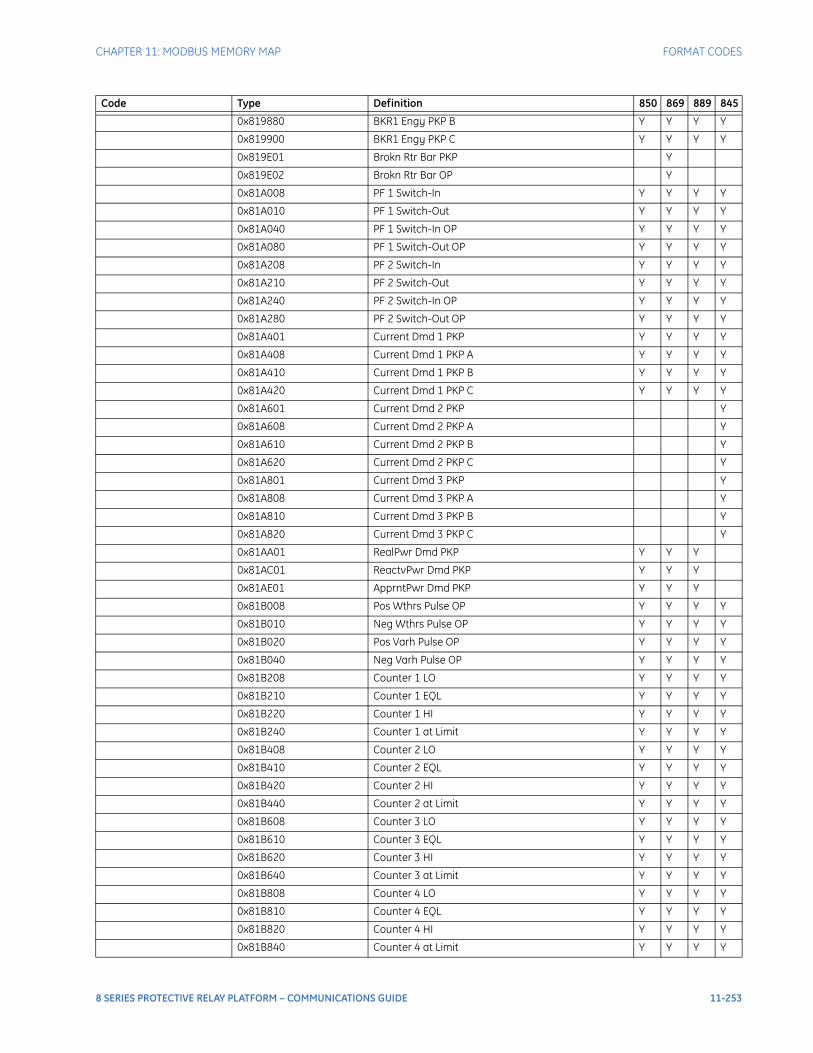
CHAPTER 11: MODBUS MEMORY MAP FORMAT CODES
0x819880 BKR1 Engy PKP B Y Y Y Y
0x819900 BKR1 Engy PKP C Y Y Y Y
0x819E01 Brokn Rtr Bar PKP Y
0x819E02 Brokn Rtr Bar OP Y
0x81A008 PF 1 Switch-In Y Y Y Y
0x81A010 PF 1 Switch-Out Y Y Y Y
0x81A040 PF 1 Switch-In OP Y Y Y Y
0x81A080 PF 1 Switch-Out OP Y Y Y Y
0x81A208 PF 2 Switch-In Y Y Y Y
0x81A210 PF 2 Switch-Out Y Y Y Y
0x81A240 PF 2 Switch-In OP Y Y Y Y
0x81A280 PF 2 Switch-Out OP Y Y Y Y
0x81A401 Current Dmd 1 PKP Y Y Y Y
0x81A408 Current Dmd 1 PKP A Y Y Y Y
0x81A410 Current Dmd 1 PKP B Y Y Y Y
0x81A420 Current Dmd 1 PKP C Y Y Y Y
0x81A601 Current Dmd 2 PKP Y
0x81A608 Current Dmd 2 PKP A Y
0x81A610 Current Dmd 2 PKP B Y
0x81A620 Current Dmd 2 PKP C Y
0x81A801 Current Dmd 3 PKP Y
0x81A808 Current Dmd 3 PKP A Y
0x81A810 Current Dmd 3 PKP B Y
0x81A820 Current Dmd 3 PKP C Y
0x81AA01 RealPwr Dmd PKP Y Y Y
0x81AC01 ReactvPwr Dmd PKP Y Y Y
0x81AE01 ApprntPwr Dmd PKP Y Y Y
0x81B008 Pos Wthrs Pulse OP Y Y Y Y
0x81B010 Neg Wthrs Pulse OP Y Y Y Y
0x81B020 Pos Varh Pulse OP Y Y Y Y
0x81B040 Neg Varh Pulse OP Y Y Y Y
0x81B208 Counter 1 LO Y Y Y Y
0x81B210 Counter 1 EQL Y Y Y Y
0x81B220 Counter 1 HI Y Y Y Y
0x81B240 Counter 1 at Limit Y Y Y Y
0x81B408 Counter 2 LO Y Y Y Y
0x81B410 Counter 2 EQL Y Y Y Y
0x81B420 Counter 2 HI Y Y Y Y
0x81B440 Counter 2 at Limit Y Y Y Y
0x81B608 Counter 3 LO Y Y Y Y
0x81B610 Counter 3 EQL Y Y Y Y
0x81B620 Counter 3 HI Y Y Y Y
0x81B640 Counter 3 at Limit Y Y Y Y
0x81B808 Counter 4 LO Y Y Y Y
0x81B810 Counter 4 EQL Y Y Y Y
0x81B820 Counter 4 HI Y Y Y Y
0x81B840 Counter 4 at Limit Y Y Y Y
Code Type Definition 850 869 889 845
8 SERIES PROTECTIVE RELAY PLATFORM – COMMUNICATIONS GUIDE 11-253
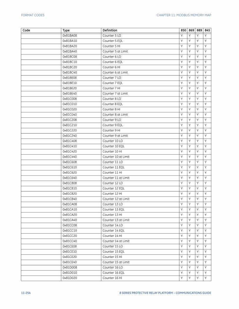
FORMAT CODES CHAPTER 11: MODBUS MEMORY MAP
0x81BA08 Counter 5 LO Y Y Y Y
0x81BA10 Counter 5 EQL Y Y Y Y
0x81BA20 Counter 5 HI Y Y Y Y
0x81BA40 Counter 5 at Limit Y Y Y Y
0x81BC08 Counter 6 LO Y Y Y Y
0x81BC10 Counter 6 EQL Y Y Y Y
0x81BC20 Counter 6 HI Y Y Y Y
0x81BC40 Counter 6 at Limit Y Y Y Y
0x81BE08 Counter 7 LO Y Y Y Y
0x81BE10 Counter 7 EQL Y Y Y Y
0x81BE20 Counter 7 HI Y Y Y Y
0x81BE40 Counter 7 at Limit Y Y Y Y
0x81C008 Counter 8 LO Y Y Y Y
0x81C010 Counter 8 EQL Y Y Y Y
0x81C020 Counter 8 HI Y Y Y Y
0x81C040 Counter 8 at Limit Y Y Y Y
0x81C208 Counter 9 LO Y Y Y Y
0x81C210 Counter 9 EQL Y Y Y Y
0x81C220 Counter 9 HI Y Y Y Y
0x81C240 Counter 9 at Limit Y Y Y Y
0x81C408 Counter 10 LO Y Y Y Y
0x81C410 Counter 10 EQL Y Y Y Y
0x81C420 Counter 10 HI Y Y Y Y
0x81C440 Counter 10 at Limit Y Y Y Y
0x81C608 Counter 11 LO Y Y Y Y
0x81C610 Counter 11 EQL Y Y Y Y
0x81C620 Counter 11 HI Y Y Y Y
0x81C640 Counter 11 at Limit Y Y Y Y
0x81C808 Counter 12 LO Y Y Y Y
0x81C810 Counter 12 EQL Y Y Y Y
0x81C820 Counter 12 HI Y Y Y Y
0x81C840 Counter 12 at Limit Y Y Y Y
0x81CA08 Counter 13 LO Y Y Y Y
0x81CA10 Counter 13 EQL Y Y Y Y
0x81CA20 Counter 13 HI Y Y Y Y
0x81CA40 Counter 13 at Limit Y Y Y Y
0x81CC08 Counter 14 LO Y Y Y Y
0x81CC10 Counter 14 EQL Y Y Y Y
0x81CC20 Counter 14 HI Y Y Y Y
0x81CC40 Counter 14 at Limit Y Y Y Y
0x81CE08 Counter 15 LO Y Y Y Y
0x81CE10 Counter 15 EQL Y Y Y Y
0x81CE20 Counter 15 HI Y Y Y Y
0x81CE40 Counter 15 at Limit Y Y Y Y
0x81D008 Counter 16 LO Y Y Y Y
0x81D010 Counter 16 EQL Y Y Y Y
0x81D020 Counter 16 HI Y Y Y Y
Code Type Definition 850 869 889 845
11-254 8 SERIES PROTECTIVE RELAY PLATFORM – COMMUNICATIONS GUIDE
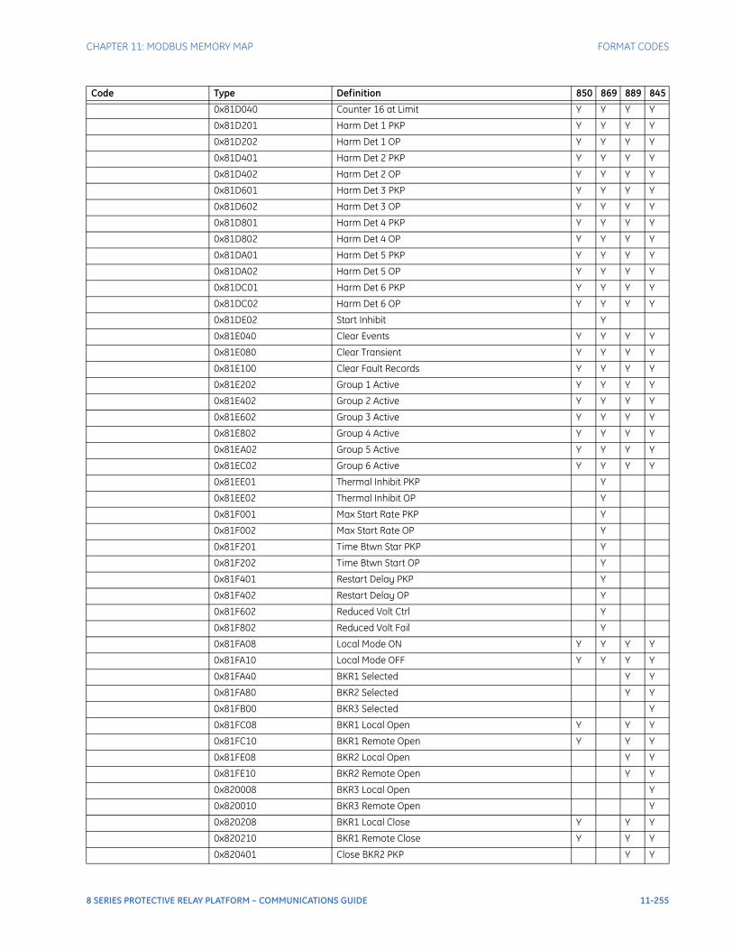
CHAPTER 11: MODBUS MEMORY MAP FORMAT CODES
0x81D040 Counter 16 at Limit Y Y Y Y
0x81D201 Harm Det 1 PKP Y Y Y Y
0x81D202 Harm Det 1 OP Y Y Y Y
0x81D401 Harm Det 2 PKP Y Y Y Y
0x81D402 Harm Det 2 OP Y Y Y Y
0x81D601 Harm Det 3 PKP Y Y Y Y
0x81D602 Harm Det 3 OP Y Y Y Y
0x81D801 Harm Det 4 PKP Y Y Y Y
0x81D802 Harm Det 4 OP Y Y Y Y
0x81DA01 Harm Det 5 PKP Y Y Y Y
0x81DA02 Harm Det 5 OP Y Y Y Y
0x81DC01 Harm Det 6 PKP Y Y Y Y
0x81DC02 Harm Det 6 OP Y Y Y Y
0x81DE02 Start Inhibit Y
0x81E040 Clear Events Y Y Y Y
0x81E080 Clear Transient Y Y Y Y
0x81E100 Clear Fault Records Y Y Y Y
0x81E202 Group 1 Active Y Y Y Y
0x81E402 Group 2 Active Y Y Y Y
0x81E602 Group 3 Active Y Y Y Y
0x81E802 Group 4 Active Y Y Y Y
0x81EA02 Group 5 Active Y Y Y Y
0x81EC02 Group 6 Active Y Y Y Y
0x81EE01 Thermal Inhibit PKP Y
0x81EE02 Thermal Inhibit OP Y
0x81F001 Max Start Rate PKP Y
0x81F002 Max Start Rate OP Y
0x81F201 Time Btwn Star PKP Y
0x81F202 Time Btwn Start OP Y
0x81F401 Restart Delay PKP Y
0x81F402 Restart Delay OP Y
0x81F602 Reduced Volt Ctrl Y
0x81F802 Reduced Volt Fail Y
0x81FA08 Local Mode ON Y Y Y Y
0x81FA10 Local Mode OFF Y Y Y Y
0x81FA40 BKR1 Selected Y Y
0x81FA80 BKR2 Selected Y Y
0x81FB00 BKR3 Selected Y
0x81FC08 BKR1 Local Open Y Y Y
0x81FC10 BKR1 Remote Open Y Y Y
0x81FE08 BKR2 Local Open Y Y
0x81FE10 BKR2 Remote Open Y Y
0x820008 BKR3 Local Open Y
0x820010 BKR3 Remote Open Y
0x820208 BKR1 Local Close Y Y Y
0x820210 BKR1 Remote Close Y Y Y
0x820401 Close BKR2 PKP Y Y
Code Type Definition 850 869 889 845
8 SERIES PROTECTIVE RELAY PLATFORM – COMMUNICATIONS GUIDE 11-255
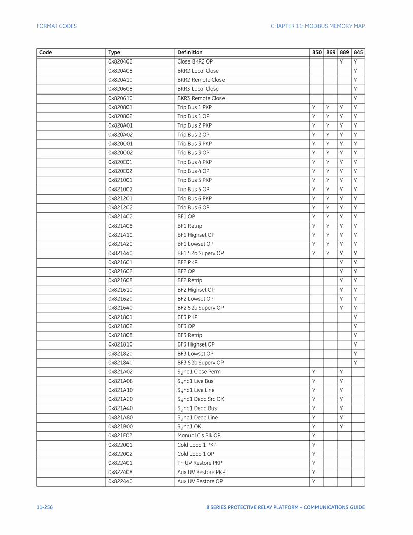
FORMAT CODES CHAPTER 11: MODBUS MEMORY MAP
0x820402 Close BKR2 OP Y Y
0x820408 BKR2 Local Close Y
0x820410 BKR2 Remote Close Y
0x820608 BKR3 Local Close Y
0x820610 BKR3 Remote Close Y
0x820801 Trip Bus 1 PKP Y Y Y Y
0x820802 Trip Bus 1 OP Y Y Y Y
0x820A01 Trip Bus 2 PKP Y Y Y Y
0x820A02 Trip Bus 2 OP Y Y Y Y
0x820C01 Trip Bus 3 PKP Y Y Y Y
0x820C02 Trip Bus 3 OP Y Y Y Y
0x820E01 Trip Bus 4 PKP Y Y Y Y
0x820E02 Trip Bus 4 OP Y Y Y Y
0x821001 Trip Bus 5 PKP Y Y Y Y
0x821002 Trip Bus 5 OP Y Y Y Y
0x821201 Trip Bus 6 PKP Y Y Y Y
0x821202 Trip Bus 6 OP Y Y Y Y
0x821402 BF1 OP Y Y Y Y
0x821408 BF1 Retrip Y Y Y Y
0x821410 BF1 Highset OP Y Y Y Y
0x821420 BF1 Lowset OP Y Y Y Y
0x821440 BF1 52b Superv OP Y Y Y Y
0x821601 BF2 PKP Y Y
0x821602 BF2 OP Y Y
0x821608 BF2 Retrip Y Y
0x821610 BF2 Highset OP Y Y
0x821620 BF2 Lowset OP Y Y
0x821640 BF2 52b Superv OP Y Y
0x821801 BF3 PKP Y
0x821802 BF3 OP Y
0x821808 BF3 Retrip Y
0x821810 BF3 Highset OP Y
0x821820 BF3 Lowset OP Y
0x821840 BF3 52b Superv OP Y
0x821A02 Sync1 Close Perm Y Y
0x821A08 Sync1 Live Bus Y Y
0x821A10 Sync1 Live Line Y Y
0x821A20 Sync1 Dead Src OK Y Y
0x821A40 Sync1 Dead Bus Y Y
0x821A80 Sync1 Dead Line Y Y
0x821B00 Sync1 OK Y Y
0x821E02 Manual Cls Blk OP Y
0x822001 Cold Load 1 PKP Y
0x822002 Cold Load 1 OP Y
0x822401 Ph UV Restore PKP Y
0x822408 Aux UV Restore PKP Y
0x822440 Aux UV Restore OP Y
Code Type Definition 850 869 889 845
11-256 8 SERIES PROTECTIVE RELAY PLATFORM – COMMUNICATIONS GUIDE
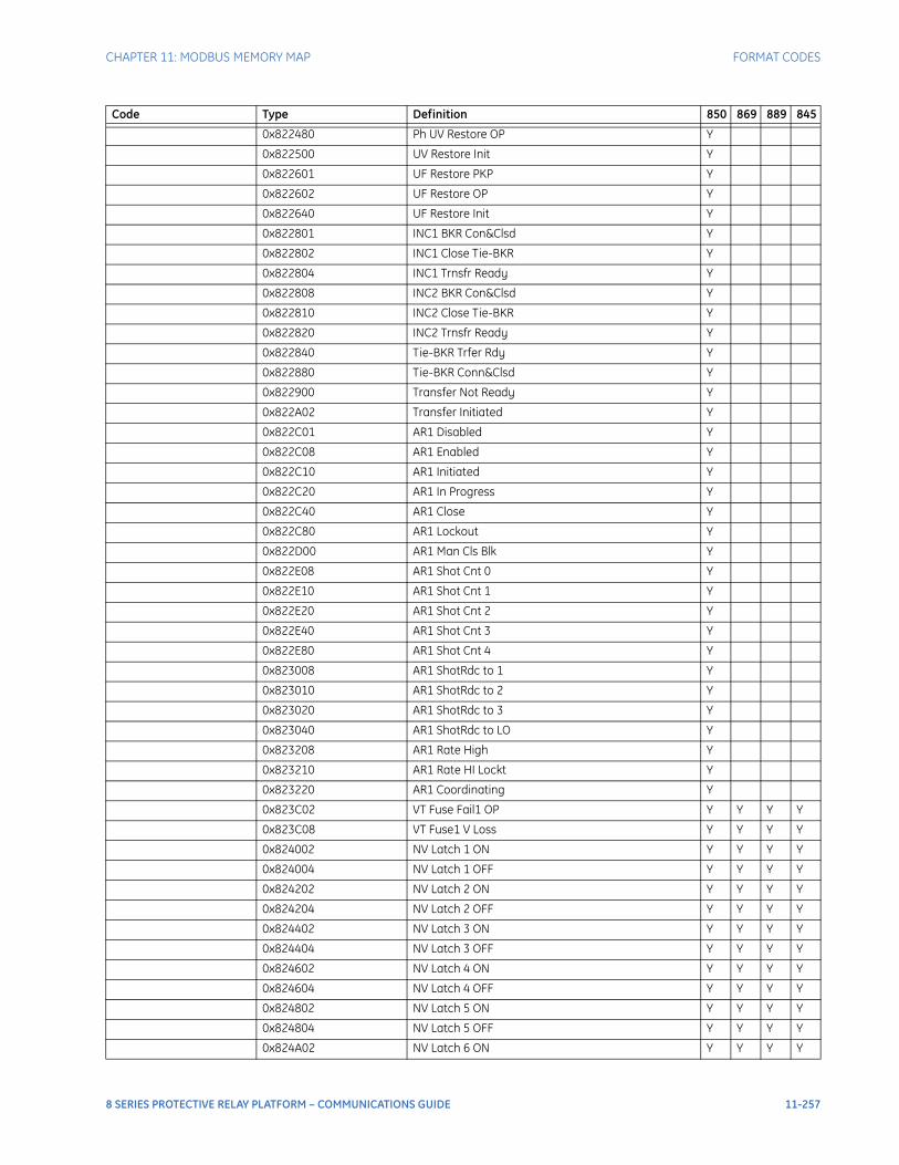
CHAPTER 11: MODBUS MEMORY MAP FORMAT CODES
0x822480 Ph UV Restore OP Y
0x822500 UV Restore Init Y
0x822601 UF Restore PKP Y
0x822602 UF Restore OP Y
0x822640 UF Restore Init Y
0x822801 INC1 BKR Con&Clsd Y
0x822802 INC1 Close Tie-BKR Y
0x822804 INC1 Trnsfr Ready Y
0x822808 INC2 BKR Con&Clsd Y
0x822810 INC2 Close Tie-BKR Y
0x822820 INC2 Trnsfr Ready Y
0x822840 Tie-BKR Trfer Rdy Y
0x822880 Tie-BKR Conn&Clsd Y
0x822900 Transfer Not Ready Y
0x822A02 Transfer Initiated Y
0x822C01 AR1 Disabled Y
0x822C08 AR1 Enabled Y
0x822C10 AR1 Initiated Y
0x822C20 AR1 In Progress Y
0x822C40 AR1 Close Y
0x822C80 AR1 Lockout Y
0x822D00 AR1 Man Cls Blk Y
0x822E08 AR1 Shot Cnt 0 Y
0x822E10 AR1 Shot Cnt 1 Y
0x822E20 AR1 Shot Cnt 2 Y
0x822E40 AR1 Shot Cnt 3 Y
0x822E80 AR1 Shot Cnt 4 Y
0x823008 AR1 ShotRdc to 1 Y
0x823010 AR1 ShotRdc to 2 Y
0x823020 AR1 ShotRdc to 3 Y
0x823040 AR1 ShotRdc to LO Y
0x823208 AR1 Rate High Y
0x823210 AR1 Rate HI Lockt Y
0x823220 AR1 Coordinating Y
0x823C02 VT Fuse Fail1 OP Y Y Y Y
0x823C08 VT Fuse1 V Loss Y Y Y Y
0x824002 NV Latch 1 ON Y Y Y Y
0x824004 NV Latch 1 OFF Y Y Y Y
0x824202 NV Latch 2 ON Y Y Y Y
0x824204 NV Latch 2 OFF Y Y Y Y
0x824402 NV Latch 3 ON Y Y Y Y
0x824404 NV Latch 3 OFF Y Y Y Y
0x824602 NV Latch 4 ON Y Y Y Y
0x824604 NV Latch 4 OFF Y Y Y Y
0x824802 NV Latch 5 ON Y Y Y Y
0x824804 NV Latch 5 OFF Y Y Y Y
0x824A02 NV Latch 6 ON Y Y Y Y
Code Type Definition 850 869 889 845
8 SERIES PROTECTIVE RELAY PLATFORM – COMMUNICATIONS GUIDE 11-257
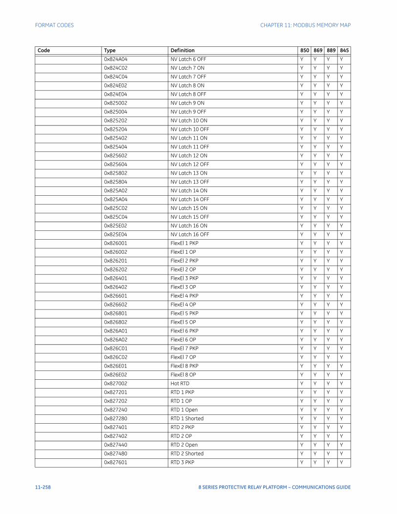
FORMAT CODES CHAPTER 11: MODBUS MEMORY MAP
0x824A04 NV Latch 6 OFF Y Y Y Y
0x824C02 NV Latch 7 ON Y Y Y Y
0x824C04 NV Latch 7 OFF Y Y Y Y
0x824E02 NV Latch 8 ON Y Y Y Y
0x824E04 NV Latch 8 OFF Y Y Y Y
0x825002 NV Latch 9 ON Y Y Y Y
0x825004 NV Latch 9 OFF Y Y Y Y
0x825202 NV Latch 10 ON Y Y Y Y
0x825204 NV Latch 10 OFF Y Y Y Y
0x825402 NV Latch 11 ON Y Y Y Y
0x825404 NV Latch 11 OFF Y Y Y Y
0x825602 NV Latch 12 ON Y Y Y Y
0x825604 NV Latch 12 OFF Y Y Y Y
0x825802 NV Latch 13 ON Y Y Y Y
0x825804 NV Latch 13 OFF Y Y Y Y
0x825A02 NV Latch 14 ON Y Y Y Y
0x825A04 NV Latch 14 OFF Y Y Y Y
0x825C02 NV Latch 15 ON Y Y Y Y
0x825C04 NV Latch 15 OFF Y Y Y Y
0x825E02 NV Latch 16 ON Y Y Y Y
0x825E04 NV Latch 16 OFF Y Y Y Y
0x826001 FlexEl 1 PKP Y Y Y Y
0x826002 FlexEl 1 OP Y Y Y Y
0x826201 FlexEl 2 PKP Y Y Y Y
0x826202 FlexEl 2 OP Y Y Y Y
0x826401 FlexEl 3 PKP Y Y Y Y
0x826402 FlexEl 3 OP Y Y Y Y
0x826601 FlexEl 4 PKP Y Y Y Y
0x826602 FlexEl 4 OP Y Y Y Y
0x826801 FlexEl 5 PKP Y Y Y Y
0x826802 FlexEl 5 OP Y Y Y Y
0x826A01 FlexEl 6 PKP Y Y Y Y
0x826A02 FlexEl 6 OP Y Y Y Y
0x826C01 FlexEl 7 PKP Y Y Y Y
0x826C02 FlexEl 7 OP Y Y Y Y
0x826E01 FlexEl 8 PKP Y Y Y Y
0x826E02 FlexEl 8 OP Y Y Y Y
0x827002 Hot RTD Y Y Y Y
0x827201 RTD 1 PKP Y Y Y Y
0x827202 RTD 1 OP Y Y Y Y
0x827240 RTD 1 Open Y Y Y Y
0x827280 RTD 1 Shorted Y Y Y Y
0x827401 RTD 2 PKP Y Y Y Y
0x827402 RTD 2 OP Y Y Y Y
0x827440 RTD 2 Open Y Y Y Y
0x827480 RTD 2 Shorted Y Y Y Y
0x827601 RTD 3 PKP Y Y Y Y
Code Type Definition 850 869 889 845
11-258 8 SERIES PROTECTIVE RELAY PLATFORM – COMMUNICATIONS GUIDE

CHAPTER 11: MODBUS MEMORY MAP FORMAT CODES
0x827602 RTD 3 OP Y Y Y Y
0x827640 RTD 3 Open Y Y Y Y
0x827680 RTD 3 Shorted Y Y Y Y
0x827801 RTD 4 PKP Y Y Y Y
0x827802 RTD 4 OP Y Y Y Y
0x827840 RTD 4 Open Y Y Y Y
0x827880 RTD 4 Shorted Y Y Y Y
0x827A01 RTD 5 PKP Y Y Y Y
0x827A02 RTD 5 OP Y Y Y Y
0x827A40 RTD 5 Open Y Y Y Y
0x827A80 RTD 5 Shorted Y Y Y Y
0x827C01 RTD 6 PKP Y Y Y Y
0x827C02 RTD 6 OP Y Y Y Y
0x827C40 RTD 6 Open Y Y Y Y
0x827C80 RTD 6 Shorted Y Y Y Y
0x827E01 RTD 7 PKP Y Y Y Y
0x827E02 RTD 7 OP Y Y Y Y
0x827E40 RTD 7 Open Y Y Y Y
0x827E80 RTD 7 Shorted Y Y Y Y
0x828001 RTD 8 PKP Y Y Y Y
0x828002 RTD 8 OP Y Y Y Y
0x828040 RTD 8 Open Y Y Y Y
0x828080 RTD 8 Shorted Y Y Y Y
0x828201 RTD 9 PKP Y Y Y Y
0x828202 RTD 9 OP Y Y Y Y
0x828240 RTD 9 Open Y Y Y Y
0x828280 RTD 9 Shorted Y Y Y Y
0x828401 RTD 10 PKP Y Y Y Y
0x828402 RTD 10 OP Y Y Y Y
0x828440 RTD 10 Open Y Y Y Y
0x828480 RTD 10 Shorted Y Y Y Y
0x828601 RTD 11 PKP Y Y Y Y
0x828602 RTD 11 OP Y Y Y Y
0x828640 RTD 11 Open Y Y Y Y
0x828680 RTD 11 Shorted Y Y Y Y
0x828801 RTD 12 PKP Y Y Y Y
0x828802 RTD 12 OP Y Y Y Y
0x828840 RTD 12 Open Y Y Y Y
0x828880 RTD 12 Shorted Y Y Y Y
0x828A01 RTD 13 PKP Y Y Y Y
0x828A02 RTD 13 OP Y Y Y Y
0x828A40 RTD 13 Open Y Y Y Y
0x828A80 RTD 13 Shorted Y Y Y Y
0x830201 Anlg Ip 1 PKP Y
0x830202 Anlg Ip 1 OP Y
0x830401 Anlg Ip 2 PKP Y
0x830402 Anlg Ip 2 OP Y
Code Type Definition 850 869 889 845
8 SERIES PROTECTIVE RELAY PLATFORM – COMMUNICATIONS GUIDE 11-259
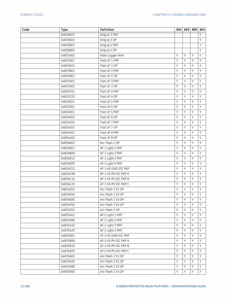
FORMAT CODES CHAPTER 11: MODBUS MEMORY MAP
0x830601 Anlg Ip 3 PKP Y
0x830602 Anlg Ip 3 OP Y
0x830801 Anlg Ip 4 PKP Y
0x830802 Anlg Ip 4 OP Y
0x833402 Data Logger Alrm Y Y Y Y
0x833601 Fast UF 1 PKP Y Y Y Y
0x833602 Fast UF 1 OP Y Y Y Y
0x833801 Fast UF 2 PKP Y Y Y Y
0x833802 Fast UF 2 OP Y Y Y Y
0x833A01 Fast UF 3 PKP Y Y Y Y
0x833A02 Fast UF 3 OP Y Y Y Y
0x833C01 Fast UF 4 PKP Y Y Y Y
0x833C02 Fast UF 4 OP Y Y Y Y
0x833E01 Fast UF 5 PKP Y Y Y Y
0x833E02 Fast UF 5 OP Y Y Y Y
0x834001 Fast UF 6 PKP Y Y Y Y
0x834002 Fast UF 6 OP Y Y Y Y
0x834201 Fast UF 7 PKP Y Y Y Y
0x834202 Fast UF 7 OP Y Y Y Y
0x834401 Fast UF 8 PKP Y Y Y Y
0x834402 Fast UF 8 OP Y Y Y Y
0x834602 Arc Flash 1 OP Y Y Y Y
0x834801 AF 1 Light 1 PKP Y Y Y Y
0x834808 AF 1 Light 2 PKP Y Y Y Y
0x834810 AF 1 Light 3 PKP Y Y Y Y
0x834820 AF 1 Light 4 PKP Y Y Y Y
0x834C01 AF 1 HS GND IOC PKP Y Y Y Y
0x834C08 AF 1 HS Ph IOC PKP A Y Y Y Y
0x834C10 AF 1 HS Ph IOC PKP B Y Y Y Y
0x834C20 AF 1 HS Ph IOC PKP C Y Y Y Y
0x834E02 Arc Flash 1 S1 OP Y Y Y Y
0x834E40 Arc Flash 1 S2 OP Y Y Y Y
0x834E80 Arc Flash 1 S3 OP Y Y Y Y
0x834F00 Arc Flash 1 S4 OP Y Y Y Y
0x835202 Arc Flash 2 OP Y Y Y Y
0x835401 AF 2 Light 1 PKP Y Y Y Y
0x835408 AF 2 Light 2 PKP Y Y Y Y
0x835410 AF 2 Light 3 PKP Y Y Y Y
0x835420 AF 2 Light 4 PKP Y Y Y Y
0x835801 AF 2 HS GND IOC PKP Y Y Y Y
0x835808 AF 2 HS Ph IOC PKP A Y Y Y Y
0x835810 AF 2 HS Ph IOC PKP B Y Y Y Y
0x835820 AF 2 HS Ph IOC PKP C Y Y Y Y
0x835A02 Arc Flash 2 S1 OP Y Y Y Y
0x835A40 Arc Flash 2 S2 OP Y Y Y Y
0x835A80 Arc Flash 2 S3 OP Y Y Y Y
0x835B00 Arc Flash 2 S4 OP Y Y Y Y
Code Type Definition 850 869 889 845
11-260 8 SERIES PROTECTIVE RELAY PLATFORM – COMMUNICATIONS GUIDE
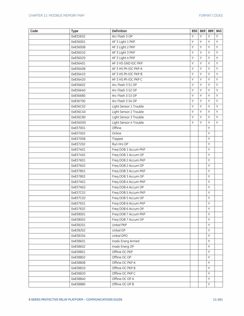
CHAPTER 11: MODBUS MEMORY MAP FORMAT CODES
0x835E02 Arc Flash 3 OP Y Y Y Y
0x836001 AF 3 Light 1 PKP Y Y Y Y
0x836008 AF 3 Light 2 PKP Y Y Y Y
0x836010 AF 3 Light 3 PKP Y Y Y Y
0x836020 AF 3 Light 4 PKP Y Y Y Y
0x836401 AF 3 HS GND IOC PKP Y Y Y Y
0x836408 AF 3 HS Ph IOC PKP A Y Y Y Y
0x836410 AF 3 HS Ph IOC PKP B Y Y Y Y
0x836420 AF 3 HS Ph IOC PKP C Y Y Y Y
0x836602 Arc Flash 3 S1 OP Y Y Y Y
0x836640 Arc Flash 3 S2 OP Y Y Y Y
0x836680 Arc Flash 3 S3 OP Y Y Y Y
0x836700 Arc Flash 3 S4 OP Y Y Y Y
0x836C02 Light Sensor 1 Trouble Y Y Y Y
0x836C40 Light Sensor 2 Trouble Y Y Y Y
0x836C80 Light Sensor 3 Trouble Y Y Y Y
0x836D00 Light Sensor 4 Trouble Y Y Y Y
0x837001 Offline Y
0x837002 Online Y
0x837008 Tripped Y
0x837202 Run Hrs OP Y
0x837401 Freq OOB 1 Accum PKP Y
0x837402 Freq OOB 1 Accum OP Y
0x837601 Freq OOB 2 Accum PKP Y
0x837602 Freq OOB 2 Accum OP Y
0x837801 Freq OOB 3 Accum PKP Y
0x837802 Freq OOB 3 Accum OP Y
0x837A01 Freq OOB 4 Accum PKP Y
0x837A02 Freq OOB 4 Accum OP Y
0x837C01 Freq OOB 5 Accum PKP Y
0x837C02 Freq OOB 5 Accum OP Y
0x837E01 Freq OOB 6 Accum PKP Y
0x837E02 Freq OOB 6 Accum OP Y
0x838001 Freq OOB 7 Accum PKP Y
0x838002 Freq OOB 7 Accum OP Y
0x838201 Unbal PKP Y
0x838202 Unbal OP Y
0x838204 Unbal DPO Y
0x838601 Inadv Energ Armed Y
0x838602 Inadv Energ OP Y
0x838801 Offline OC PKP Y
0x838802 Offline OC OP Y
0x838808 Offline OC PKP A Y
0x838810 Offline OC PKP B Y
0x838820 Offline OC PKP C Y
0x838840 Offline OC OP A Y
0x838880 Offline OC OP B Y
Code Type Definition 850 869 889 845
8 SERIES PROTECTIVE RELAY PLATFORM – COMMUNICATIONS GUIDE 11-261
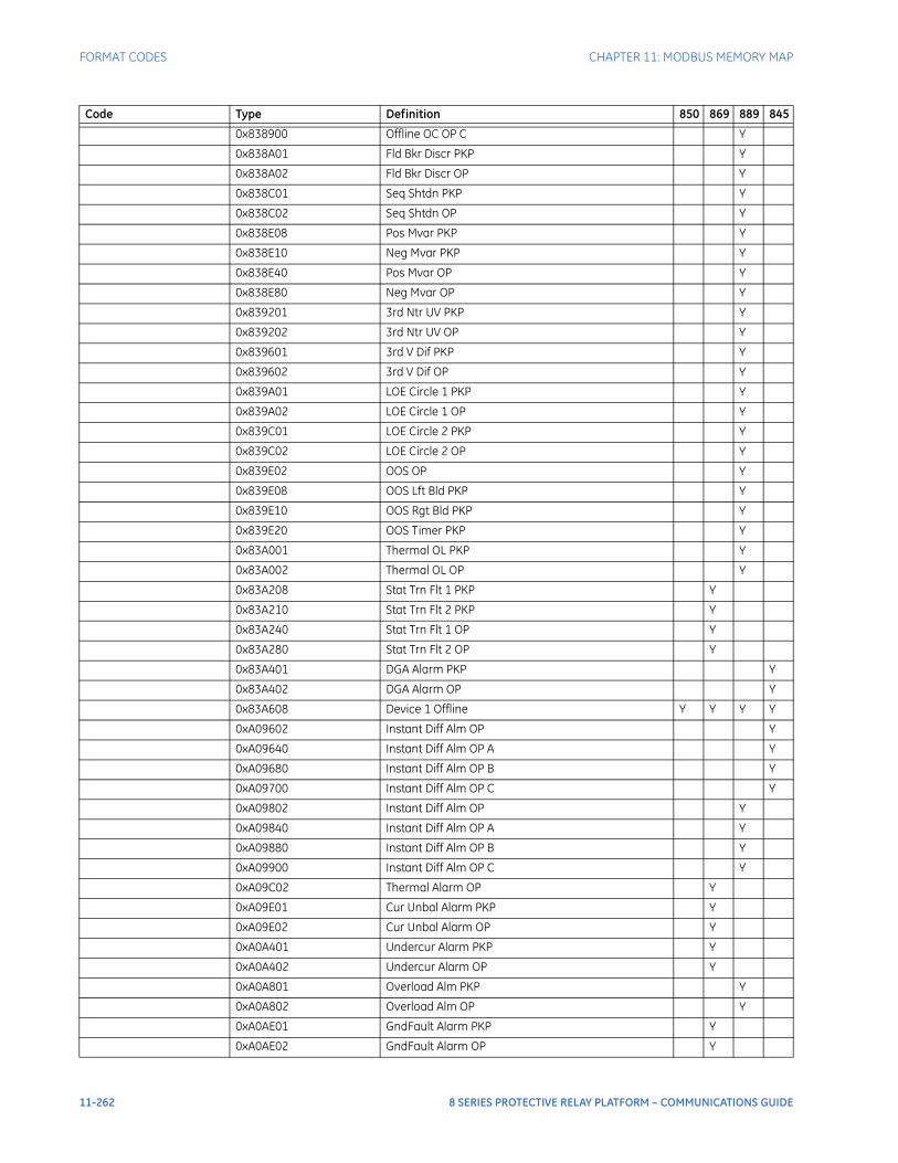
FORMAT CODES CHAPTER 11: MODBUS MEMORY MAP
0x838900 Offline OC OP C Y
0x838A01 Fld Bkr Discr PKP Y
0x838A02 Fld Bkr Discr OP Y
0x838C01 Seq Shtdn PKP Y
0x838C02 Seq Shtdn OP Y
0x838E08 Pos Mvar PKP Y
0x838E10 Neg Mvar PKP Y
0x838E40 Pos Mvar OP Y
0x838E80 Neg Mvar OP Y
0x839201 3rd Ntr UV PKP Y
0x839202 3rd Ntr UV OP Y
0x839601 3rd V Dif PKP Y
0x839602 3rd V Dif OP Y
0x839A01 LOE Circle 1 PKP Y
0x839A02 LOE Circle 1 OP Y
0x839C01 LOE Circle 2 PKP Y
0x839C02 LOE Circle 2 OP Y
0x839E02 OOS OP Y
0x839E08 OOS Lft Bld PKP Y
0x839E10 OOS Rgt Bld PKP Y
0x839E20 OOS Timer PKP Y
0x83A001 Thermal OL PKP Y
0x83A002 Thermal OL OP Y
0x83A208 Stat Trn Flt 1 PKP Y
0x83A210 Stat Trn Flt 2 PKP Y
0x83A240 Stat Trn Flt 1 OP Y
0x83A280 Stat Trn Flt 2 OP Y
0x83A401 DGA Alarm PKP Y
0x83A402 DGA Alarm OP Y
0x83A608 Device 1 Offline Y Y Y Y
0xA09602 Instant Diff Alm OP Y
0xA09640 Instant Diff Alm OP A Y
0xA09680 Instant Diff Alm OP B Y
0xA09700 Instant Diff Alm OP C Y
0xA09802 Instant Diff Alm OP Y
0xA09840 Instant Diff Alm OP A Y
0xA09880 Instant Diff Alm OP B Y
0xA09900 Instant Diff Alm OP C Y
0xA09C02 Thermal Alarm OP Y
0xA09E01 Cur Unbal Alarm PKP Y
0xA09E02 Cur Unbal Alarm OP Y
0xA0A401 Undercur Alarm PKP Y
0xA0A402 Undercur Alarm OP Y
0xA0A801 Overload Alm PKP Y
0xA0A802 Overload Alm OP Y
0xA0AE01 GndFault Alarm PKP Y
0xA0AE02 GndFault Alarm OP Y
Code Type Definition 850 869 889 845
11-262 8 SERIES PROTECTIVE RELAY PLATFORM – COMMUNICATIONS GUIDE
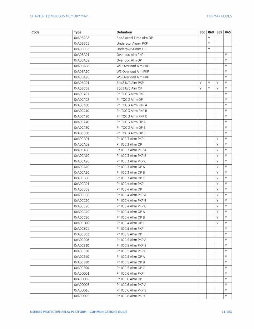
CHAPTER 11: MODBUS MEMORY MAP FORMAT CODES
0xA0B402 Spd2 Accel Time Alm OP Y
0xA0B601 Underpwr Alarm PKP Y
0xA0B602 Underpwr Alarm OP Y
0xA0BA01 Overload Alm PKP Y
0xA0BA02 Overload Alm OP Y
0xA0BA08 W1 Overload Alm PKP Y
0xA0BA10 W2 Overload Alm PKP Y
0xA0BA20 W3 Overload Alm PKP Y
0xA0BC01 Spd2 U/C Alm PKP Y Y Y Y
0xA0BC02 Spd2 U/C Alm OP Y Y Y Y
0xA0C401 Ph TOC 3 Alrm PKP Y
0xA0C402 Ph TOC 3 Alrm OP Y
0xA0C408 Ph TOC 3 Alrm PKP A Y
0xA0C410 Ph TOC 3 Alrm PKP B Y
0xA0C420 Ph TOC 3 Alrm PKP C Y
0xA0C440 Ph TOC 3 Alrm OP A Y
0xA0C480 Ph TOC 3 Alrm OP B Y
0xA0C500 Ph TOC 3 Alrm OP C Y
0xA0CA01 Ph IOC 3 Alrm PKP Y Y
0xA0CA02 Ph IOC 3 Alrm OP Y Y
0xA0CA08 Ph IOC 3 Alrm PKP A Y Y
0xA0CA10 Ph IOC 3 Alrm PKP B Y Y
0xA0CA20 Ph IOC 3 Alrm PKP C Y Y
0xA0CA40 Ph IOC 3 Alrm OP A Y Y
0xA0CA80 Ph IOC 3 Alrm OP B Y Y
0xA0CB00 Ph IOC 3 Alrm OP C Y Y
0xA0CC01 Ph IOC 4 Alrm PKP Y Y
0xA0CC02 Ph IOC 4 Alrm OP Y Y
0xA0CC08 Ph IOC 4 Alrm PKP A Y Y
0xA0CC10 Ph IOC 4 Alrm PKP B Y Y
0xA0CC20 Ph IOC 4 Alrm PKP C Y Y
0xA0CC40 Ph IOC 4 Alrm OP A Y Y
0xA0CC80 Ph IOC 4 Alrm OP B Y Y
0xA0CD00 Ph IOC 4 Alrm OP C Y Y
0xA0CE01 Ph IOC 5 Alrm PKP Y
0xA0CE02 Ph IOC 5 Alrm OP Y
0xA0CE08 Ph IOC 5 Alrm PKP A Y
0xA0CE10 Ph IOC 5 Alrm PKP B Y
0xA0CE20 Ph IOC 5 Alrm PKP C Y
0xA0CE40 Ph IOC 5 Alrm OP A Y
0xA0CE80 Ph IOC 5 Alrm OP B Y
0xA0CF00 Ph IOC 5 Alrm OP C Y
0xA0D001 Ph IOC 6 Alrm PKP Y
0xA0D002 Ph IOC 6 Alrm OP Y
0xA0D008 Ph IOC 6 Alrm PKP A Y
0xA0D010 Ph IOC 6 Alrm PKP B Y
0xA0D020 Ph IOC 6 Alrm PKP C Y
Code Type Definition 850 869 889 845
8 SERIES PROTECTIVE RELAY PLATFORM – COMMUNICATIONS GUIDE 11-263
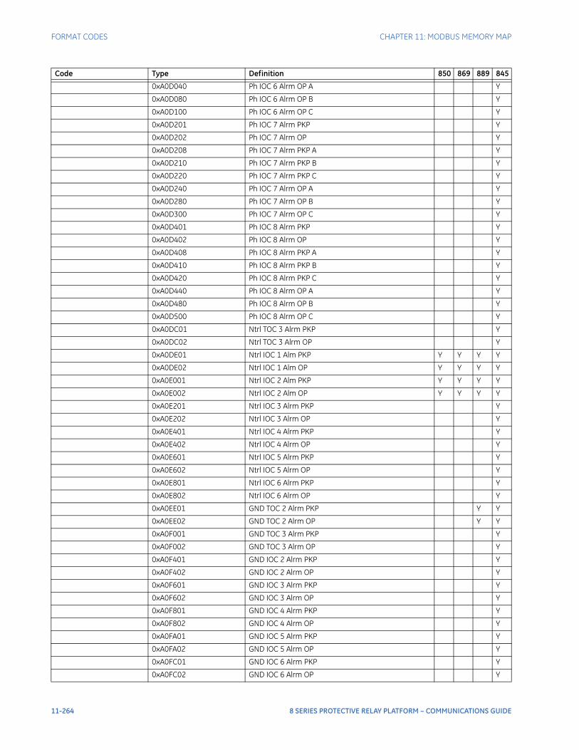
FORMAT CODES CHAPTER 11: MODBUS MEMORY MAP
0xA0D040 Ph IOC 6 Alrm OP A Y
0xA0D080 Ph IOC 6 Alrm OP B Y
0xA0D100 Ph IOC 6 Alrm OP C Y
0xA0D201 Ph IOC 7 Alrm PKP Y
0xA0D202 Ph IOC 7 Alrm OP Y
0xA0D208 Ph IOC 7 Alrm PKP A Y
0xA0D210 Ph IOC 7 Alrm PKP B Y
0xA0D220 Ph IOC 7 Alrm PKP C Y
0xA0D240 Ph IOC 7 Alrm OP A Y
0xA0D280 Ph IOC 7 Alrm OP B Y
0xA0D300 Ph IOC 7 Alrm OP C Y
0xA0D401 Ph IOC 8 Alrm PKP Y
0xA0D402 Ph IOC 8 Alrm OP Y
0xA0D408 Ph IOC 8 Alrm PKP A Y
0xA0D410 Ph IOC 8 Alrm PKP B Y
0xA0D420 Ph IOC 8 Alrm PKP C Y
0xA0D440 Ph IOC 8 Alrm OP A Y
0xA0D480 Ph IOC 8 Alrm OP B Y
0xA0D500 Ph IOC 8 Alrm OP C Y
0xA0DC01 Ntrl TOC 3 Alrm PKP Y
0xA0DC02 Ntrl TOC 3 Alrm OP Y
0xA0DE01 Ntrl IOC 1 Alm PKP Y Y Y Y
0xA0DE02 Ntrl IOC 1 Alm OP Y Y Y Y
0xA0E001 Ntrl IOC 2 Alm PKP Y Y Y Y
0xA0E002 Ntrl IOC 2 Alm OP Y Y Y Y
0xA0E201 Ntrl IOC 3 Alrm PKP Y
0xA0E202 Ntrl IOC 3 Alrm OP Y
0xA0E401 Ntrl IOC 4 Alrm PKP Y
0xA0E402 Ntrl IOC 4 Alrm OP Y
0xA0E601 Ntrl IOC 5 Alrm PKP Y
0xA0E602 Ntrl IOC 5 Alrm OP Y
0xA0E801 Ntrl IOC 6 Alrm PKP Y
0xA0E802 Ntrl IOC 6 Alrm OP Y
0xA0EE01 GND TOC 2 Alrm PKP Y Y
0xA0EE02 GND TOC 2 Alrm OP Y Y
0xA0F001 GND TOC 3 Alrm PKP Y
0xA0F002 GND TOC 3 Alrm OP Y
0xA0F401 GND IOC 2 Alrm PKP Y
0xA0F402 GND IOC 2 Alrm OP Y
0xA0F601 GND IOC 3 Alrm PKP Y
0xA0F602 GND IOC 3 Alrm OP Y
0xA0F801 GND IOC 4 Alrm PKP Y
0xA0F802 GND IOC 4 Alrm OP Y
0xA0FA01 GND IOC 5 Alrm PKP Y
0xA0FA02 GND IOC 5 Alrm OP Y
0xA0FC01 GND IOC 6 Alrm PKP Y
0xA0FC02 GND IOC 6 Alrm OP Y
Code Type Definition 850 869 889 845
11-264 8 SERIES PROTECTIVE RELAY PLATFORM – COMMUNICATIONS GUIDE
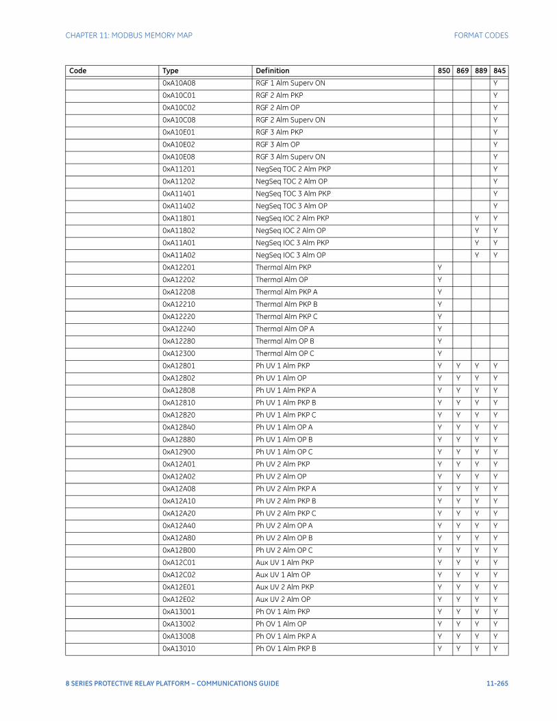
CHAPTER 11: MODBUS MEMORY MAP FORMAT CODES
0xA10A08 RGF 1 Alm Superv ON Y
0xA10C01 RGF 2 Alm PKP Y
0xA10C02 RGF 2 Alm OP Y
0xA10C08 RGF 2 Alm Superv ON Y
0xA10E01 RGF 3 Alm PKP Y
0xA10E02 RGF 3 Alm OP Y
0xA10E08 RGF 3 Alm Superv ON Y
0xA11201 NegSeq TOC 2 Alm PKP Y
0xA11202 NegSeq TOC 2 Alm OP Y
0xA11401 NegSeq TOC 3 Alm PKP Y
0xA11402 NegSeq TOC 3 Alm OP Y
0xA11801 NegSeq IOC 2 Alm PKP Y Y
0xA11802 NegSeq IOC 2 Alm OP Y Y
0xA11A01 NegSeq IOC 3 Alm PKP Y Y
0xA11A02 NegSeq IOC 3 Alm OP Y Y
0xA12201 Thermal Alm PKP Y
0xA12202 Thermal Alm OP Y
0xA12208 Thermal Alm PKP A Y
0xA12210 Thermal Alm PKP B Y
0xA12220 Thermal Alm PKP C Y
0xA12240 Thermal Alm OP A Y
0xA12280 Thermal Alm OP B Y
0xA12300 Thermal Alm OP C Y
0xA12801 Ph UV 1 Alm PKP Y Y Y Y
0xA12802 Ph UV 1 Alm OP Y Y Y Y
0xA12808 Ph UV 1 Alm PKP A Y Y Y Y
0xA12810 Ph UV 1 Alm PKP B Y Y Y Y
0xA12820 Ph UV 1 Alm PKP C Y Y Y Y
0xA12840 Ph UV 1 Alm OP A Y Y Y Y
0xA12880 Ph UV 1 Alm OP B Y Y Y Y
0xA12900 Ph UV 1 Alm OP C Y Y Y Y
0xA12A01 Ph UV 2 Alm PKP Y Y Y Y
0xA12A02 Ph UV 2 Alm OP Y Y Y Y
0xA12A08 Ph UV 2 Alm PKP A Y Y Y Y
0xA12A10 Ph UV 2 Alm PKP B Y Y Y Y
0xA12A20 Ph UV 2 Alm PKP C Y Y Y Y
0xA12A40 Ph UV 2 Alm OP A Y Y Y Y
0xA12A80 Ph UV 2 Alm OP B Y Y Y Y
0xA12B00 Ph UV 2 Alm OP C Y Y Y Y
0xA12C01 Aux UV 1 Alm PKP Y Y Y Y
0xA12C02 Aux UV 1 Alm OP Y Y Y Y
0xA12E01 Aux UV 2 Alm PKP Y Y Y Y
0xA12E02 Aux UV 2 Alm OP Y Y Y Y
0xA13001 Ph OV 1 Alm PKP Y Y Y Y
0xA13002 Ph OV 1 Alm OP Y Y Y Y
0xA13008 Ph OV 1 Alm PKP A Y Y Y Y
0xA13010 Ph OV 1 Alm PKP B Y Y Y Y
Code Type Definition 850 869 889 845
8 SERIES PROTECTIVE RELAY PLATFORM – COMMUNICATIONS GUIDE 11-265
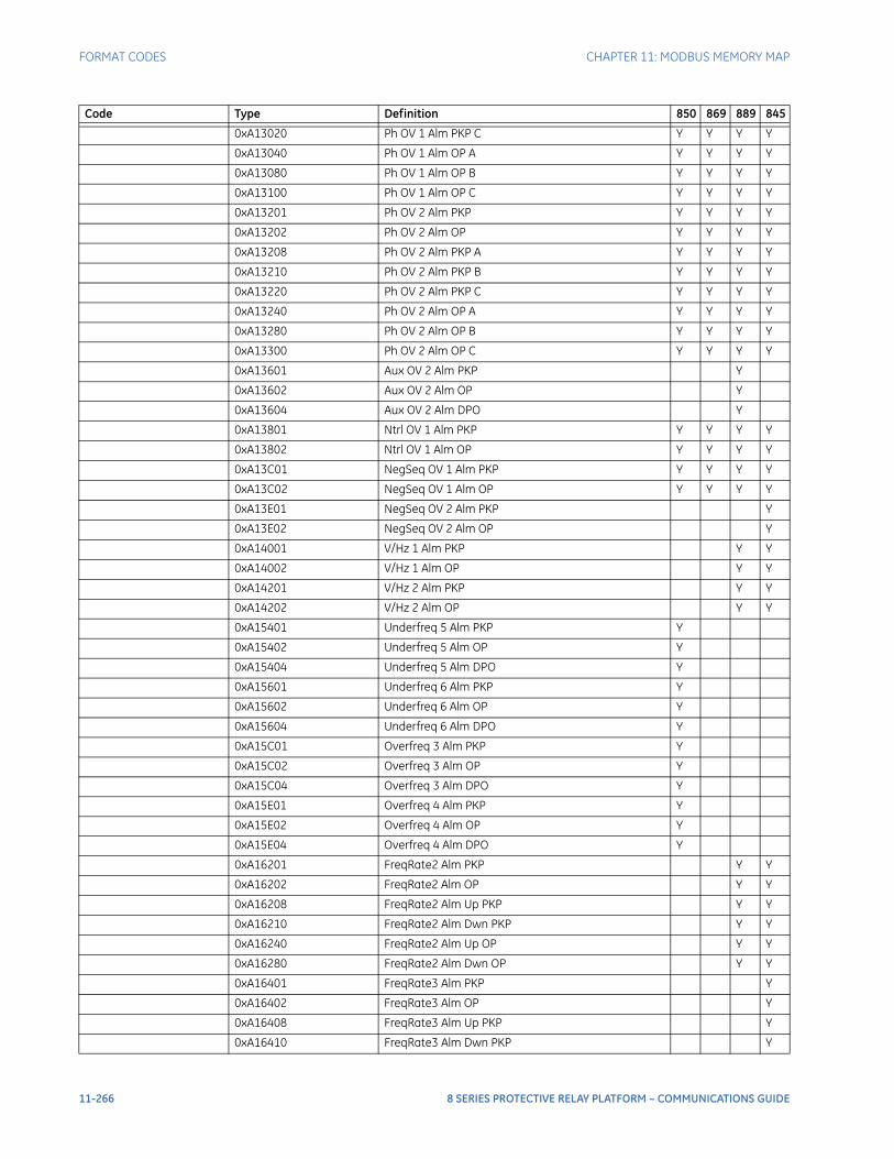
FORMAT CODES CHAPTER 11: MODBUS MEMORY MAP
0xA13020 Ph OV 1 Alm PKP C Y Y Y Y
0xA13040 Ph OV 1 Alm OP A Y Y Y Y
0xA13080 Ph OV 1 Alm OP B Y Y Y Y
0xA13100 Ph OV 1 Alm OP C Y Y Y Y
0xA13201 Ph OV 2 Alm PKP Y Y Y Y
0xA13202 Ph OV 2 Alm OP Y Y Y Y
0xA13208 Ph OV 2 Alm PKP A Y Y Y Y
0xA13210 Ph OV 2 Alm PKP B Y Y Y Y
0xA13220 Ph OV 2 Alm PKP C Y Y Y Y
0xA13240 Ph OV 2 Alm OP A Y Y Y Y
0xA13280 Ph OV 2 Alm OP B Y Y Y Y
0xA13300 Ph OV 2 Alm OP C Y Y Y Y
0xA13601 Aux OV 2 Alm PKP Y
0xA13602 Aux OV 2 Alm OP Y
0xA13604 Aux OV 2 Alm DPO Y
0xA13801 Ntrl OV 1 Alm PKP Y Y Y Y
0xA13802 Ntrl OV 1 Alm OP Y Y Y Y
0xA13C01 NegSeq OV 1 Alm PKP Y Y Y Y
0xA13C02 NegSeq OV 1 Alm OP Y Y Y Y
0xA13E01 NegSeq OV 2 Alm PKP Y
0xA13E02 NegSeq OV 2 Alm OP Y
0xA14001 V/Hz 1 Alm PKP Y Y
0xA14002 V/Hz 1 Alm OP Y Y
0xA14201 V/Hz 2 Alm PKP Y Y
0xA14202 V/Hz 2 Alm OP Y Y
0xA15401 Underfreq 5 Alm PKP Y
0xA15402 Underfreq 5 Alm OP Y
0xA15404 Underfreq 5 Alm DPO Y
0xA15601 Underfreq 6 Alm PKP Y
0xA15602 Underfreq 6 Alm OP Y
0xA15604 Underfreq 6 Alm DPO Y
0xA15C01 Overfreq 3 Alm PKP Y
0xA15C02 Overfreq 3 Alm OP Y
0xA15C04 Overfreq 3 Alm DPO Y
0xA15E01 Overfreq 4 Alm PKP Y
0xA15E02 Overfreq 4 Alm OP Y
0xA15E04 Overfreq 4 Alm DPO Y
0xA16201 FreqRate2 Alm PKP Y Y
0xA16202 FreqRate2 Alm OP Y Y
0xA16208 FreqRate2 Alm Up PKP Y Y
0xA16210 FreqRate2 Alm Dwn PKP Y Y
0xA16240 FreqRate2 Alm Up OP Y Y
0xA16280 FreqRate2 Alm Dwn OP Y Y
0xA16401 FreqRate3 Alm PKP Y
0xA16402 FreqRate3 Alm OP Y
0xA16408 FreqRate3 Alm Up PKP Y
0xA16410 FreqRate3 Alm Dwn PKP Y
Code Type Definition 850 869 889 845
11-266 8 SERIES PROTECTIVE RELAY PLATFORM – COMMUNICATIONS GUIDE
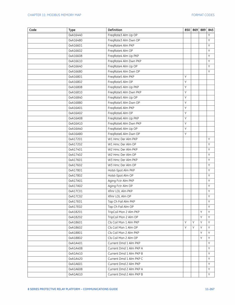
CHAPTER 11: MODBUS MEMORY MAP FORMAT CODES
0xA16440 FreqRate3 Alm Up OP Y
0xA16480 FreqRate3 Alm Dwn OP Y
0xA16601 FreqRate4 Alm PKP Y
0xA16602 FreqRate4 Alm OP Y
0xA16608 FreqRate4 Alm Up PKP Y
0xA16610 FreqRate4 Alm Dwn PKP Y
0xA16640 FreqRate4 Alm Up OP Y
0xA16680 FreqRate4 Alm Dwn OP Y
0xA16801 FreqRate5 Alm PKP Y
0xA16802 FreqRate5 Alm OP Y
0xA16808 FreqRate5 Alm Up PKP Y
0xA16810 FreqRate5 Alm Dwn PKP Y
0xA16840 FreqRate5 Alm Up OP Y
0xA16880 FreqRate5 Alm Dwn OP Y
0xA16A01 FreqRate6 Alm PKP Y
0xA16A02 FreqRate6 Alm OP Y
0xA16A08 FreqRate6 Alm Up PKP Y
0xA16A10 FreqRate6 Alm Dwn PKP Y
0xA16A40 FreqRate6 Alm Up OP Y
0xA16A80 FreqRate6 Alm Dwn OP Y
0xA17201 W1 Hmc Der Alm PKP Y
0xA17202 W1 Hmc Der Alm OP Y
0xA17401 W2 Hmc Der Alm PKP Y
0xA17402 W2 Hmc Der Alm OP Y
0xA17601 W3 Hmc Der Alm PKP Y
0xA17602 W3 Hmc Der Alm OP Y
0xA17801 Hotst-Spot Alm PKP Y
0xA17802 Hotst-Spot Alm OP Y
0xA17A01 Aging Fctr Alm PKP Y
0xA17A02 Aging Fctr Alm OP Y
0xA17C01 Xfmr LOL Alm PKP Y
0xA17C02 Xfmr LOL Alm OP Y
0xA17E01 Tap Ch Fail Alm PKP Y
0xA17E02 Tap Ch Fail Alm OP Y
0xA18201 TripCoil Mon 2 Alm PKP Y Y
0xA18202 TripCoil Mon 2 Alm OP Y Y
0xA18601 Cls Coil Mon 1 Alm PKP Y Y Y Y
0xA18602 Cls Coil Mon 1 Alm OP Y Y Y Y
0xA18801 Cls Coil Mon 2 Alm PKP Y Y
0xA18802 Cls Coil Mon 2 Alm OP Y Y
0xA1A401 Current Dmd 1 Alm PKP Y
0xA1A408 Current Dmd 1 Alm PKP A Y
0xA1A410 Current Dmd 1 Alm PKP B Y
0xA1A420 Current Dmd 1 Alm PKP C Y
0xA1A601 Current Dmd 2 Alm PKP Y
0xA1A608 Current Dmd 2 Alm PKP A Y
0xA1A610 Current Dmd 2 Alm PKP B Y
Code Type Definition 850 869 889 845
8 SERIES PROTECTIVE RELAY PLATFORM – COMMUNICATIONS GUIDE 11-267
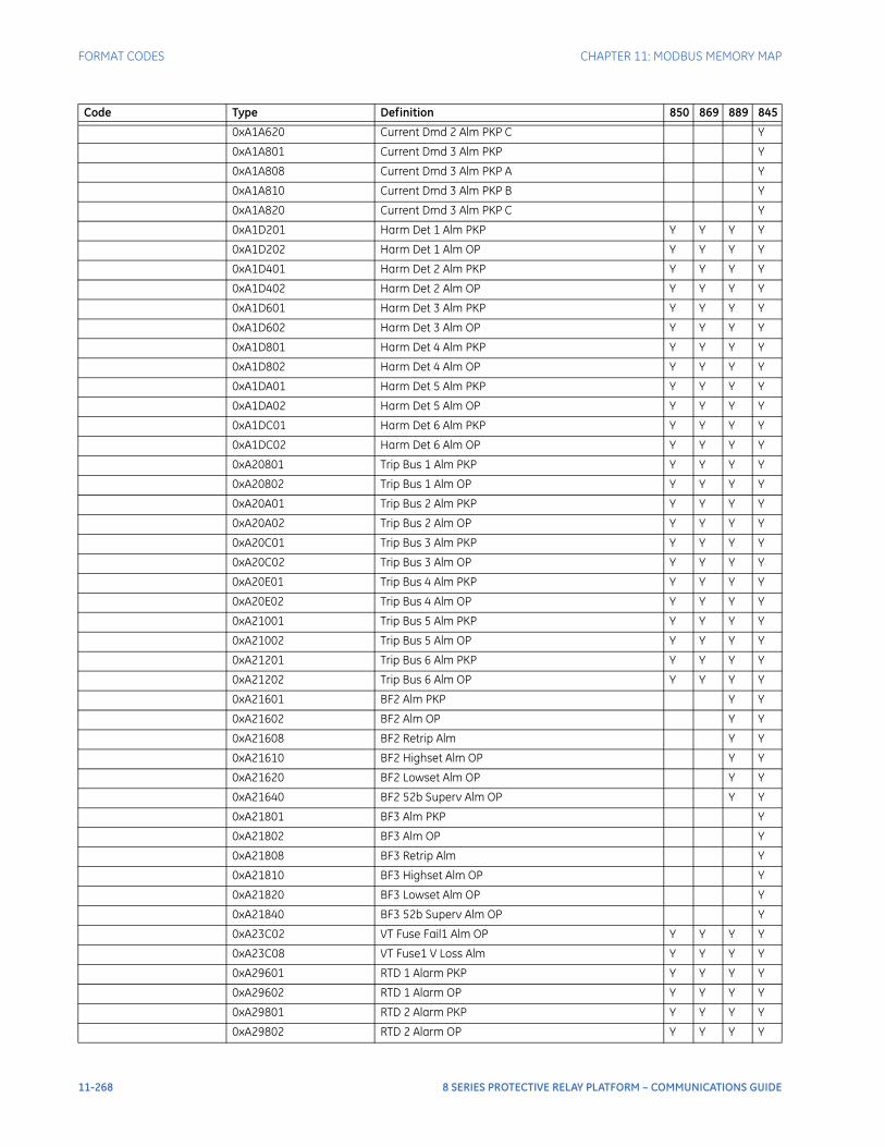
FORMAT CODES CHAPTER 11: MODBUS MEMORY MAP
0xA1A620 Current Dmd 2 Alm PKP C Y
0xA1A801 Current Dmd 3 Alm PKP Y
0xA1A808 Current Dmd 3 Alm PKP A Y
0xA1A810 Current Dmd 3 Alm PKP B Y
0xA1A820 Current Dmd 3 Alm PKP C Y
0xA1D201 Harm Det 1 Alm PKP Y Y Y Y
0xA1D202 Harm Det 1 Alm OP Y Y Y Y
0xA1D401 Harm Det 2 Alm PKP Y Y Y Y
0xA1D402 Harm Det 2 Alm OP Y Y Y Y
0xA1D601 Harm Det 3 Alm PKP Y Y Y Y
0xA1D602 Harm Det 3 Alm OP Y Y Y Y
0xA1D801 Harm Det 4 Alm PKP Y Y Y Y
0xA1D802 Harm Det 4 Alm OP Y Y Y Y
0xA1DA01 Harm Det 5 Alm PKP Y Y Y Y
0xA1DA02 Harm Det 5 Alm OP Y Y Y Y
0xA1DC01 Harm Det 6 Alm PKP Y Y Y Y
0xA1DC02 Harm Det 6 Alm OP Y Y Y Y
0xA20801 Trip Bus 1 Alm PKP Y Y Y Y
0xA20802 Trip Bus 1 Alm OP Y Y Y Y
0xA20A01 Trip Bus 2 Alm PKP Y Y Y Y
0xA20A02 Trip Bus 2 Alm OP Y Y Y Y
0xA20C01 Trip Bus 3 Alm PKP Y Y Y Y
0xA20C02 Trip Bus 3 Alm OP Y Y Y Y
0xA20E01 Trip Bus 4 Alm PKP Y Y Y Y
0xA20E02 Trip Bus 4 Alm OP Y Y Y Y
0xA21001 Trip Bus 5 Alm PKP Y Y Y Y
0xA21002 Trip Bus 5 Alm OP Y Y Y Y
0xA21201 Trip Bus 6 Alm PKP Y Y Y Y
0xA21202 Trip Bus 6 Alm OP Y Y Y Y
0xA21601 BF2 Alm PKP Y Y
0xA21602 BF2 Alm OP Y Y
0xA21608 BF2 Retrip Alm Y Y
0xA21610 BF2 Highset Alm OP Y Y
0xA21620 BF2 Lowset Alm OP Y Y
0xA21640 BF2 52b Superv Alm OP Y Y
0xA21801 BF3 Alm PKP Y
0xA21802 BF3 Alm OP Y
0xA21808 BF3 Retrip Alm Y
0xA21810 BF3 Highset Alm OP Y
0xA21820 BF3 Lowset Alm OP Y
0xA21840 BF3 52b Superv Alm OP Y
0xA23C02 VT Fuse Fail1 Alm OP Y Y Y Y
0xA23C08 VT Fuse1 V Loss Alm Y Y Y Y
0xA29601 RTD 1 Alarm PKP Y Y Y Y
0xA29602 RTD 1 Alarm OP Y Y Y Y
0xA29801 RTD 2 Alarm PKP Y Y Y Y
0xA29802 RTD 2 Alarm OP Y Y Y Y
Code Type Definition 850 869 889 845
11-268 8 SERIES PROTECTIVE RELAY PLATFORM – COMMUNICATIONS GUIDE
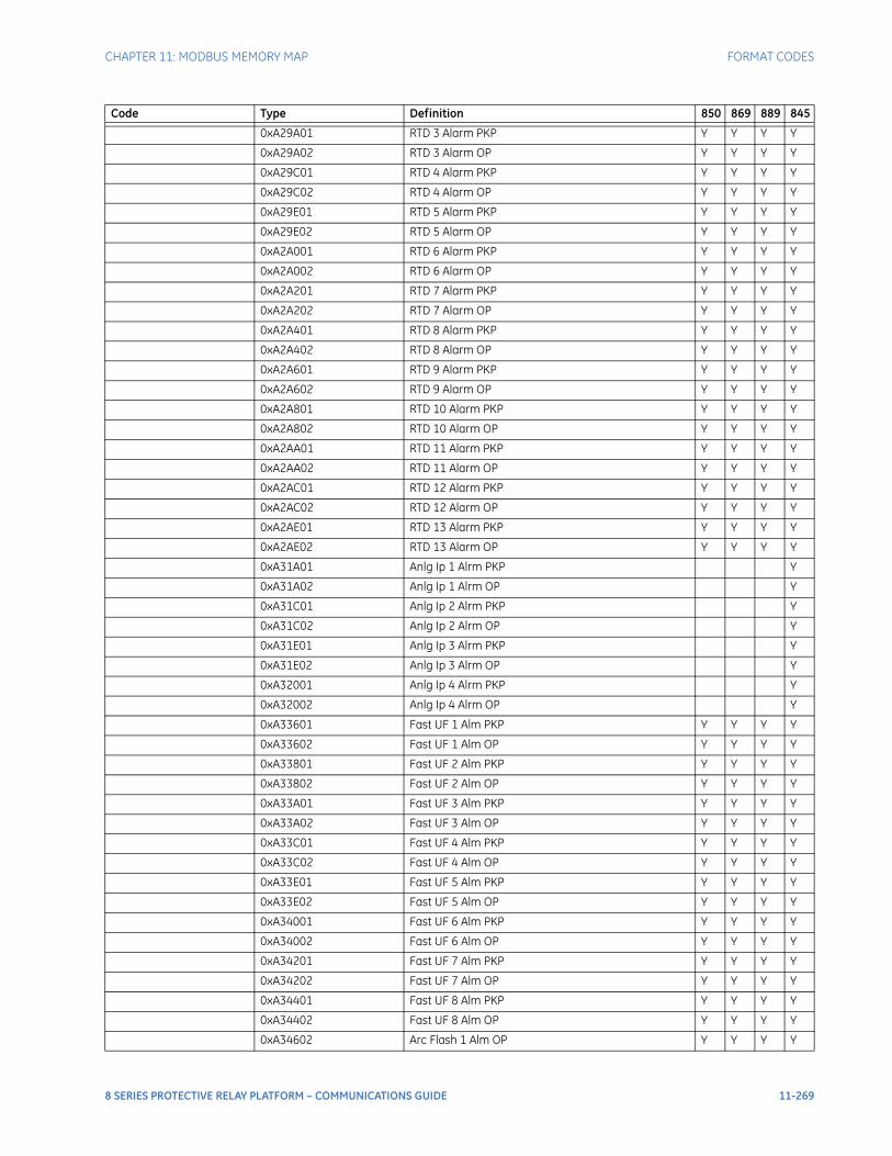
CHAPTER 11: MODBUS MEMORY MAP FORMAT CODES
0xA29A01 RTD 3 Alarm PKP Y Y Y Y
0xA29A02 RTD 3 Alarm OP Y Y Y Y
0xA29C01 RTD 4 Alarm PKP Y Y Y Y
0xA29C02 RTD 4 Alarm OP Y Y Y Y
0xA29E01 RTD 5 Alarm PKP Y Y Y Y
0xA29E02 RTD 5 Alarm OP Y Y Y Y
0xA2A001 RTD 6 Alarm PKP Y Y Y Y
0xA2A002 RTD 6 Alarm OP Y Y Y Y
0xA2A201 RTD 7 Alarm PKP Y Y Y Y
0xA2A202 RTD 7 Alarm OP Y Y Y Y
0xA2A401 RTD 8 Alarm PKP Y Y Y Y
0xA2A402 RTD 8 Alarm OP Y Y Y Y
0xA2A601 RTD 9 Alarm PKP Y Y Y Y
0xA2A602 RTD 9 Alarm OP Y Y Y Y
0xA2A801 RTD 10 Alarm PKP Y Y Y Y
0xA2A802 RTD 10 Alarm OP Y Y Y Y
0xA2AA01 RTD 11 Alarm PKP Y Y Y Y
0xA2AA02 RTD 11 Alarm OP Y Y Y Y
0xA2AC01 RTD 12 Alarm PKP Y Y Y Y
0xA2AC02 RTD 12 Alarm OP Y Y Y Y
0xA2AE01 RTD 13 Alarm PKP Y Y Y Y
0xA2AE02 RTD 13 Alarm OP Y Y Y Y
0xA31A01 Anlg Ip 1 Alrm PKP Y
0xA31A02 Anlg Ip 1 Alrm OP Y
0xA31C01 Anlg Ip 2 Alrm PKP Y
0xA31C02 Anlg Ip 2 Alrm OP Y
0xA31E01 Anlg Ip 3 Alrm PKP Y
0xA31E02 Anlg Ip 3 Alrm OP Y
0xA32001 Anlg Ip 4 Alrm PKP Y
0xA32002 Anlg Ip 4 Alrm OP Y
0xA33601 Fast UF 1 Alm PKP Y Y Y Y
0xA33602 Fast UF 1 Alm OP Y Y Y Y
0xA33801 Fast UF 2 Alm PKP Y Y Y Y
0xA33802 Fast UF 2 Alm OP Y Y Y Y
0xA33A01 Fast UF 3 Alm PKP Y Y Y Y
0xA33A02 Fast UF 3 Alm OP Y Y Y Y
0xA33C01 Fast UF 4 Alm PKP Y Y Y Y
0xA33C02 Fast UF 4 Alm OP Y Y Y Y
0xA33E01 Fast UF 5 Alm PKP Y Y Y Y
0xA33E02 Fast UF 5 Alm OP Y Y Y Y
0xA34001 Fast UF 6 Alm PKP Y Y Y Y
0xA34002 Fast UF 6 Alm OP Y Y Y Y
0xA34201 Fast UF 7 Alm PKP Y Y Y Y
0xA34202 Fast UF 7 Alm OP Y Y Y Y
0xA34401 Fast UF 8 Alm PKP Y Y Y Y
0xA34402 Fast UF 8 Alm OP Y Y Y Y
0xA34602 Arc Flash 1 Alm OP Y Y Y Y
Code Type Definition 850 869 889 845
8 SERIES PROTECTIVE RELAY PLATFORM – COMMUNICATIONS GUIDE 11-269
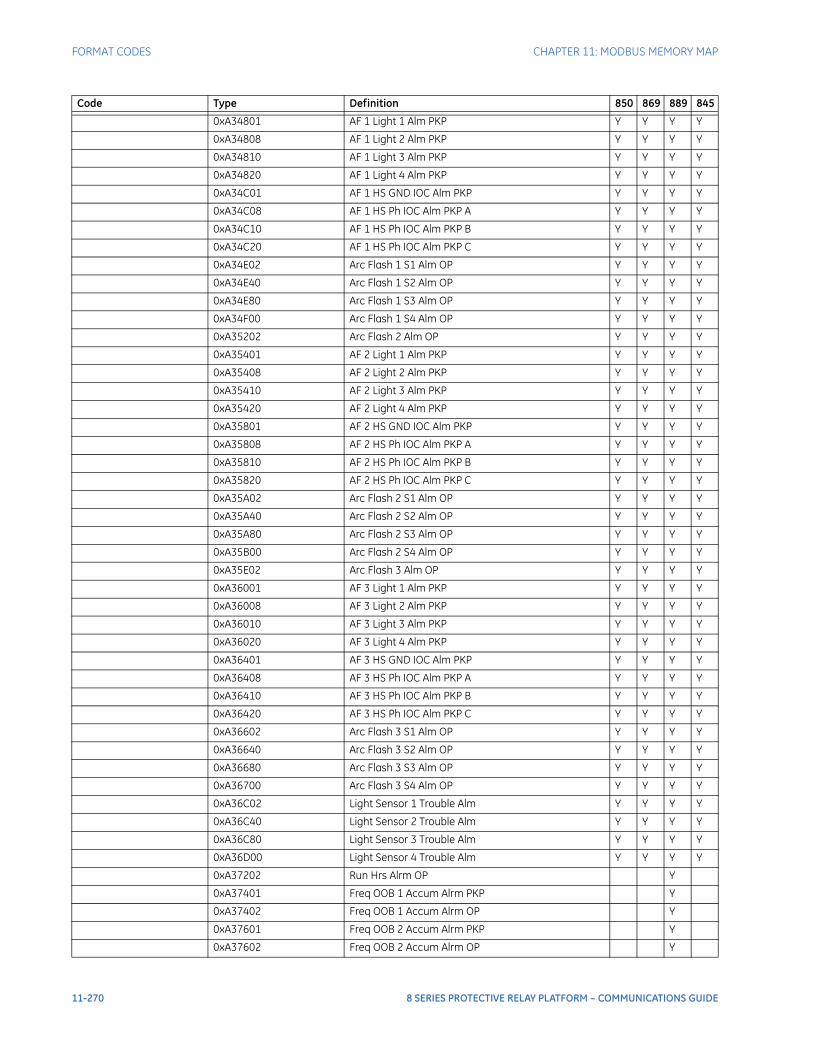
FORMAT CODES CHAPTER 11: MODBUS MEMORY MAP
0xA34801 AF 1 Light 1 Alm PKP Y Y Y Y
0xA34808 AF 1 Light 2 Alm PKP Y Y Y Y
0xA34810 AF 1 Light 3 Alm PKP Y Y Y Y
0xA34820 AF 1 Light 4 Alm PKP Y Y Y Y
0xA34C01 AF 1 HS GND IOC Alm PKP Y Y Y Y
0xA34C08 AF 1 HS Ph IOC Alm PKP A Y Y Y Y
0xA34C10 AF 1 HS Ph IOC Alm PKP B Y Y Y Y
0xA34C20 AF 1 HS Ph IOC Alm PKP C Y Y Y Y
0xA34E02 Arc Flash 1 S1 Alm OP Y Y Y Y
0xA34E40 Arc Flash 1 S2 Alm OP Y Y Y Y
0xA34E80 Arc Flash 1 S3 Alm OP Y Y Y Y
0xA34F00 Arc Flash 1 S4 Alm OP Y Y Y Y
0xA35202 Arc Flash 2 Alm OP Y Y Y Y
0xA35401 AF 2 Light 1 Alm PKP Y Y Y Y
0xA35408 AF 2 Light 2 Alm PKP Y Y Y Y
0xA35410 AF 2 Light 3 Alm PKP Y Y Y Y
0xA35420 AF 2 Light 4 Alm PKP Y Y Y Y
0xA35801 AF 2 HS GND IOC Alm PKP Y Y Y Y
0xA35808 AF 2 HS Ph IOC Alm PKP A Y Y Y Y
0xA35810 AF 2 HS Ph IOC Alm PKP B Y Y Y Y
0xA35820 AF 2 HS Ph IOC Alm PKP C Y Y Y Y
0xA35A02 Arc Flash 2 S1 Alm OP Y Y Y Y
0xA35A40 Arc Flash 2 S2 Alm OP Y Y Y Y
0xA35A80 Arc Flash 2 S3 Alm OP Y Y Y Y
0xA35B00 Arc Flash 2 S4 Alm OP Y Y Y Y
0xA35E02 Arc Flash 3 Alm OP Y Y Y Y
0xA36001 AF 3 Light 1 Alm PKP Y Y Y Y
0xA36008 AF 3 Light 2 Alm PKP Y Y Y Y
0xA36010 AF 3 Light 3 Alm PKP Y Y Y Y
0xA36020 AF 3 Light 4 Alm PKP Y Y Y Y
0xA36401 AF 3 HS GND IOC Alm PKP Y Y Y Y
0xA36408 AF 3 HS Ph IOC Alm PKP A Y Y Y Y
0xA36410 AF 3 HS Ph IOC Alm PKP B Y Y Y Y
0xA36420 AF 3 HS Ph IOC Alm PKP C Y Y Y Y
0xA36602 Arc Flash 3 S1 Alm OP Y Y Y Y
0xA36640 Arc Flash 3 S2 Alm OP Y Y Y Y
0xA36680 Arc Flash 3 S3 Alm OP Y Y Y Y
0xA36700 Arc Flash 3 S4 Alm OP Y Y Y Y
0xA36C02 Light Sensor 1 Trouble Alm Y Y Y Y
0xA36C40 Light Sensor 2 Trouble Alm Y Y Y Y
0xA36C80 Light Sensor 3 Trouble Alm Y Y Y Y
0xA36D00 Light Sensor 4 Trouble Alm Y Y Y Y
0xA37202 Run Hrs Alrm OP Y
0xA37401 Freq OOB 1 Accum Alrm PKP Y
0xA37402 Freq OOB 1 Accum Alrm OP Y
0xA37601 Freq OOB 2 Accum Alrm PKP Y
0xA37602 Freq OOB 2 Accum Alrm OP Y
Code Type Definition 850 869 889 845
11-270 8 SERIES PROTECTIVE RELAY PLATFORM – COMMUNICATIONS GUIDE
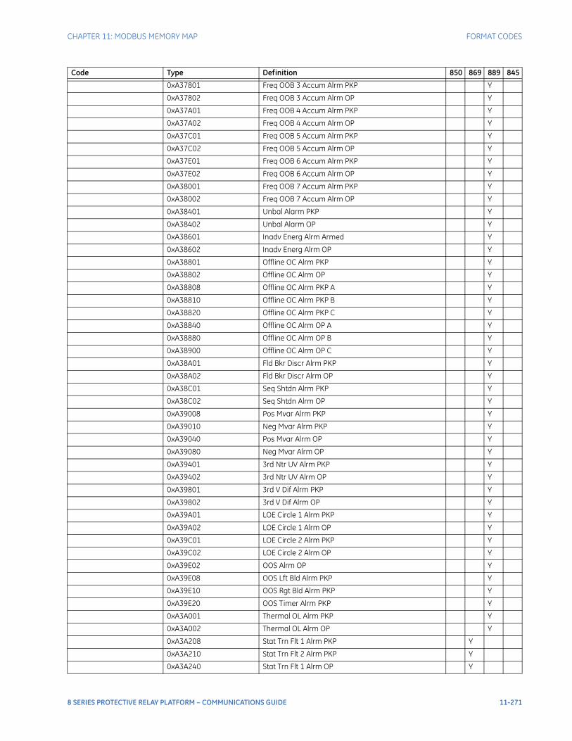
CHAPTER 11: MODBUS MEMORY MAP FORMAT CODES
0xA37801 Freq OOB 3 Accum Alrm PKP Y
0xA37802 Freq OOB 3 Accum Alrm OP Y
0xA37A01 Freq OOB 4 Accum Alrm PKP Y
0xA37A02 Freq OOB 4 Accum Alrm OP Y
0xA37C01 Freq OOB 5 Accum Alrm PKP Y
0xA37C02 Freq OOB 5 Accum Alrm OP Y
0xA37E01 Freq OOB 6 Accum Alrm PKP Y
0xA37E02 Freq OOB 6 Accum Alrm OP Y
0xA38001 Freq OOB 7 Accum Alrm PKP Y
0xA38002 Freq OOB 7 Accum Alrm OP Y
0xA38401 Unbal Alarm PKP Y
0xA38402 Unbal Alarm OP Y
0xA38601 Inadv Energ Alrm Armed Y
0xA38602 Inadv Energ Alrm OP Y
0xA38801 Offline OC Alrm PKP Y
0xA38802 Offline OC Alrm OP Y
0xA38808 Offline OC Alrm PKP A Y
0xA38810 Offline OC Alrm PKP B Y
0xA38820 Offline OC Alrm PKP C Y
0xA38840 Offline OC Alrm OP A Y
0xA38880 Offline OC Alrm OP B Y
0xA38900 Offline OC Alrm OP C Y
0xA38A01 Fld Bkr Discr Alrm PKP Y
0xA38A02 Fld Bkr Discr Alrm OP Y
0xA38C01 Seq Shtdn Alrm PKP Y
0xA38C02 Seq Shtdn Alrm OP Y
0xA39008 Pos Mvar Alrm PKP Y
0xA39010 Neg Mvar Alrm PKP Y
0xA39040 Pos Mvar Alrm OP Y
0xA39080 Neg Mvar Alrm OP Y
0xA39401 3rd Ntr UV Alrm PKP Y
0xA39402 3rd Ntr UV Alrm OP Y
0xA39801 3rd V Dif Alrm PKP Y
0xA39802 3rd V Dif Alrm OP Y
0xA39A01 LOE Circle 1 Alrm PKP Y
0xA39A02 LOE Circle 1 Alrm OP Y
0xA39C01 LOE Circle 2 Alrm PKP Y
0xA39C02 LOE Circle 2 Alrm OP Y
0xA39E02 OOS Alrm OP Y
0xA39E08 OOS Lft Bld Alrm PKP Y
0xA39E10 OOS Rgt Bld Alrm PKP Y
0xA39E20 OOS Timer Alrm PKP Y
0xA3A001 Thermal OL Alrm PKP Y
0xA3A002 Thermal OL Alrm OP Y
0xA3A208 Stat Trn Flt 1 Alrm PKP Y
0xA3A210 Stat Trn Flt 2 Alrm PKP Y
0xA3A240 Stat Trn Flt 1 Alrm OP Y
Code Type Definition 850 869 889 845
8 SERIES PROTECTIVE RELAY PLATFORM – COMMUNICATIONS GUIDE 11-271
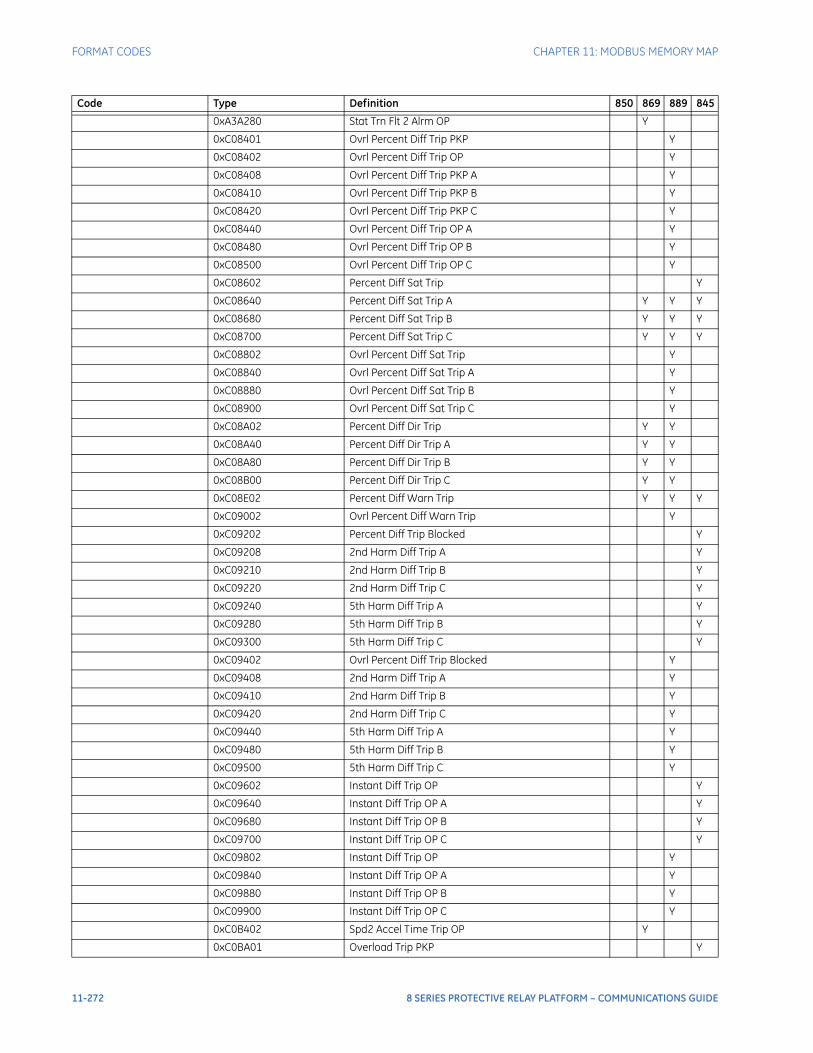
FORMAT CODES CHAPTER 11: MODBUS MEMORY MAP
0xA3A280 Stat Trn Flt 2 Alrm OP Y
0xC08401 Ovrl Percent Diff Trip PKP Y
0xC08402 Ovrl Percent Diff Trip OP Y
0xC08408 Ovrl Percent Diff Trip PKP A Y
0xC08410 Ovrl Percent Diff Trip PKP B Y
0xC08420 Ovrl Percent Diff Trip PKP C Y
0xC08440 Ovrl Percent Diff Trip OP A Y
0xC08480 Ovrl Percent Diff Trip OP B Y
0xC08500 Ovrl Percent Diff Trip OP C Y
0xC08602 Percent Diff Sat Trip Y
0xC08640 Percent Diff Sat Trip A Y Y Y
0xC08680 Percent Diff Sat Trip B Y Y Y
0xC08700 Percent Diff Sat Trip C Y Y Y
0xC08802 Ovrl Percent Diff Sat Trip Y
0xC08840 Ovrl Percent Diff Sat Trip A Y
0xC08880 Ovrl Percent Diff Sat Trip B Y
0xC08900 Ovrl Percent Diff Sat Trip C Y
0xC08A02 Percent Diff Dir Trip Y Y
0xC08A40 Percent Diff Dir Trip A Y Y
0xC08A80 Percent Diff Dir Trip B Y Y
0xC08B00 Percent Diff Dir Trip C Y Y
0xC08E02 Percent Diff Warn Trip Y Y Y
0xC09002 Ovrl Percent Diff Warn Trip Y
0xC09202 Percent Diff Trip Blocked Y
0xC09208 2nd Harm Diff Trip A Y
0xC09210 2nd Harm Diff Trip B Y
0xC09220 2nd Harm Diff Trip C Y
0xC09240 5th Harm Diff Trip A Y
0xC09280 5th Harm Diff Trip B Y
0xC09300 5th Harm Diff Trip C Y
0xC09402 Ovrl Percent Diff Trip Blocked Y
0xC09408 2nd Harm Diff Trip A Y
0xC09410 2nd Harm Diff Trip B Y
0xC09420 2nd Harm Diff Trip C Y
0xC09440 5th Harm Diff Trip A Y
0xC09480 5th Harm Diff Trip B Y
0xC09500 5th Harm Diff Trip C Y
0xC09602 Instant Diff Trip OP Y
0xC09640 Instant Diff Trip OP A Y
0xC09680 Instant Diff Trip OP B Y
0xC09700 Instant Diff Trip OP C Y
0xC09802 Instant Diff Trip OP Y
0xC09840 Instant Diff Trip OP A Y
0xC09880 Instant Diff Trip OP B Y
0xC09900 Instant Diff Trip OP C Y
0xC0B402 Spd2 Accel Time Trip OP Y
0xC0BA01 Overload Trip PKP Y
Code Type Definition 850 869 889 845
11-272 8 SERIES PROTECTIVE RELAY PLATFORM – COMMUNICATIONS GUIDE
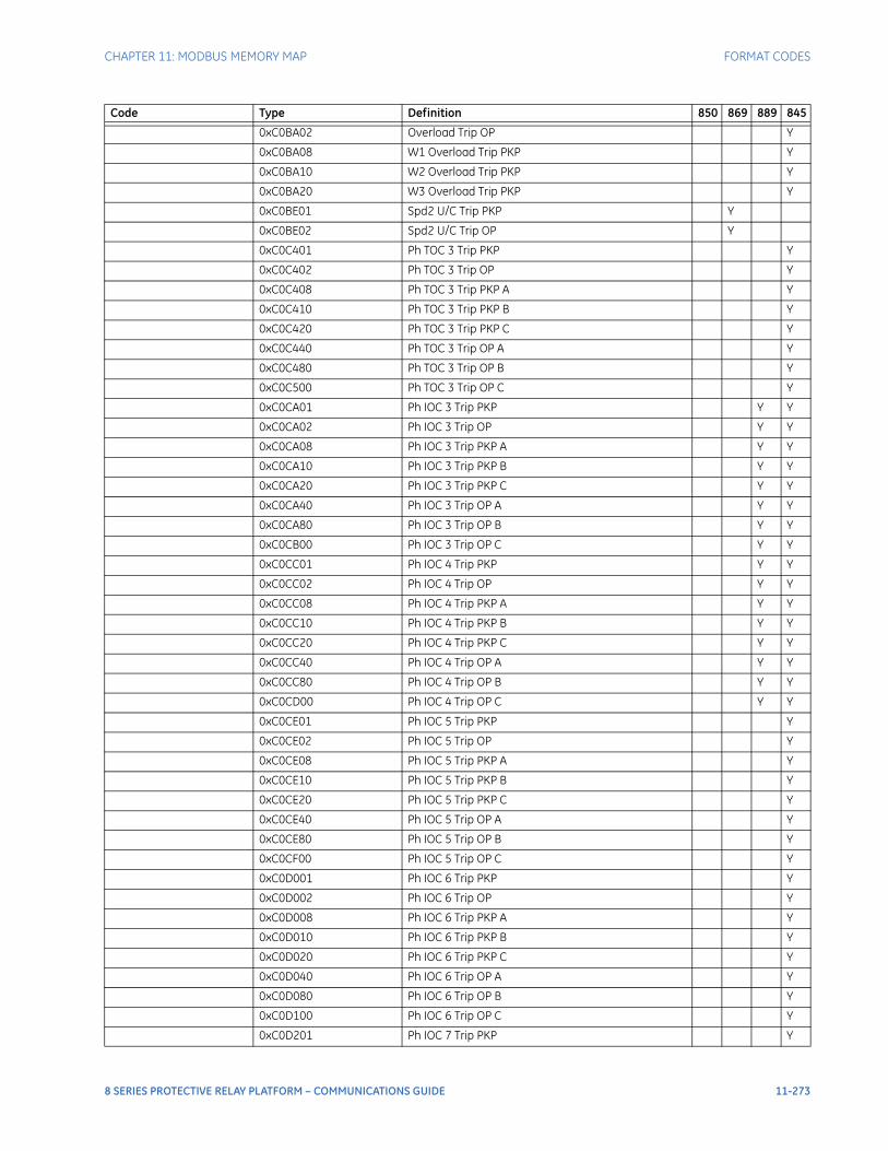
CHAPTER 11: MODBUS MEMORY MAP FORMAT CODES
0xC0BA02 Overload Trip OP Y
0xC0BA08 W1 Overload Trip PKP Y
0xC0BA10 W2 Overload Trip PKP Y
0xC0BA20 W3 Overload Trip PKP Y
0xC0BE01 Spd2 U/C Trip PKP Y
0xC0BE02 Spd2 U/C Trip OP Y
0xC0C401 Ph TOC 3 Trip PKP Y
0xC0C402 Ph TOC 3 Trip OP Y
0xC0C408 Ph TOC 3 Trip PKP A Y
0xC0C410 Ph TOC 3 Trip PKP B Y
0xC0C420 Ph TOC 3 Trip PKP C Y
0xC0C440 Ph TOC 3 Trip OP A Y
0xC0C480 Ph TOC 3 Trip OP B Y
0xC0C500 Ph TOC 3 Trip OP C Y
0xC0CA01 Ph IOC 3 Trip PKP Y Y
0xC0CA02 Ph IOC 3 Trip OP Y Y
0xC0CA08 Ph IOC 3 Trip PKP A Y Y
0xC0CA10 Ph IOC 3 Trip PKP B Y Y
0xC0CA20 Ph IOC 3 Trip PKP C Y Y
0xC0CA40 Ph IOC 3 Trip OP A Y Y
0xC0CA80 Ph IOC 3 Trip OP B Y Y
0xC0CB00 Ph IOC 3 Trip OP C Y Y
0xC0CC01 Ph IOC 4 Trip PKP Y Y
0xC0CC02 Ph IOC 4 Trip OP Y Y
0xC0CC08 Ph IOC 4 Trip PKP A Y Y
0xC0CC10 Ph IOC 4 Trip PKP B Y Y
0xC0CC20 Ph IOC 4 Trip PKP C Y Y
0xC0CC40 Ph IOC 4 Trip OP A Y Y
0xC0CC80 Ph IOC 4 Trip OP B Y Y
0xC0CD00 Ph IOC 4 Trip OP C Y Y
0xC0CE01 Ph IOC 5 Trip PKP Y
0xC0CE02 Ph IOC 5 Trip OP Y
0xC0CE08 Ph IOC 5 Trip PKP A Y
0xC0CE10 Ph IOC 5 Trip PKP B Y
0xC0CE20 Ph IOC 5 Trip PKP C Y
0xC0CE40 Ph IOC 5 Trip OP A Y
0xC0CE80 Ph IOC 5 Trip OP B Y
0xC0CF00 Ph IOC 5 Trip OP C Y
0xC0D001 Ph IOC 6 Trip PKP Y
0xC0D002 Ph IOC 6 Trip OP Y
0xC0D008 Ph IOC 6 Trip PKP A Y
0xC0D010 Ph IOC 6 Trip PKP B Y
0xC0D020 Ph IOC 6 Trip PKP C Y
0xC0D040 Ph IOC 6 Trip OP A Y
0xC0D080 Ph IOC 6 Trip OP B Y
0xC0D100 Ph IOC 6 Trip OP C Y
0xC0D201 Ph IOC 7 Trip PKP Y
Code Type Definition 850 869 889 845
8 SERIES PROTECTIVE RELAY PLATFORM – COMMUNICATIONS GUIDE 11-273
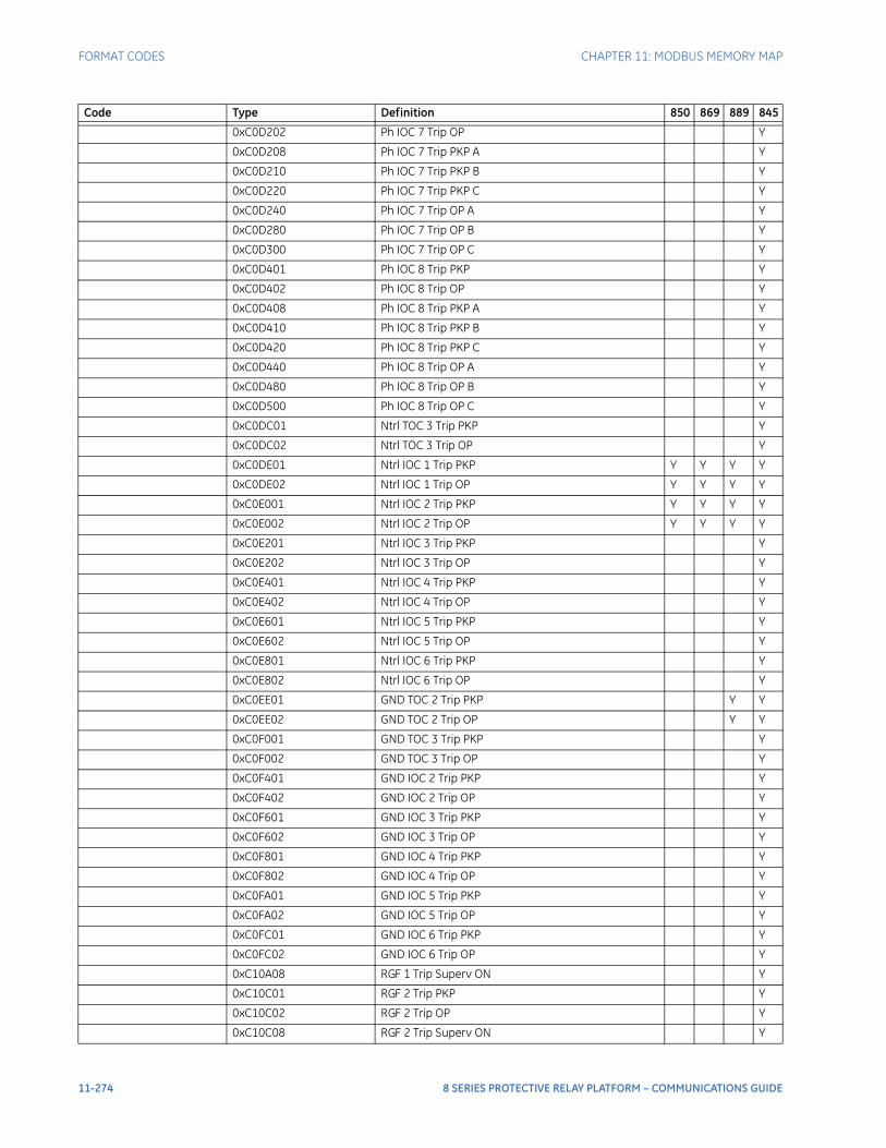
FORMAT CODES CHAPTER 11: MODBUS MEMORY MAP
0xC0D202 Ph IOC 7 Trip OP Y
0xC0D208 Ph IOC 7 Trip PKP A Y
0xC0D210 Ph IOC 7 Trip PKP B Y
0xC0D220 Ph IOC 7 Trip PKP C Y
0xC0D240 Ph IOC 7 Trip OP A Y
0xC0D280 Ph IOC 7 Trip OP B Y
0xC0D300 Ph IOC 7 Trip OP C Y
0xC0D401 Ph IOC 8 Trip PKP Y
0xC0D402 Ph IOC 8 Trip OP Y
0xC0D408 Ph IOC 8 Trip PKP A Y
0xC0D410 Ph IOC 8 Trip PKP B Y
0xC0D420 Ph IOC 8 Trip PKP C Y
0xC0D440 Ph IOC 8 Trip OP A Y
0xC0D480 Ph IOC 8 Trip OP B Y
0xC0D500 Ph IOC 8 Trip OP C Y
0xC0DC01 Ntrl TOC 3 Trip PKP Y
0xC0DC02 Ntrl TOC 3 Trip OP Y
0xC0DE01 Ntrl IOC 1 Trip PKP Y Y Y Y
0xC0DE02 Ntrl IOC 1 Trip OP Y Y Y Y
0xC0E001 Ntrl IOC 2 Trip PKP Y Y Y Y
0xC0E002 Ntrl IOC 2 Trip OP Y Y Y Y
0xC0E201 Ntrl IOC 3 Trip PKP Y
0xC0E202 Ntrl IOC 3 Trip OP Y
0xC0E401 Ntrl IOC 4 Trip PKP Y
0xC0E402 Ntrl IOC 4 Trip OP Y
0xC0E601 Ntrl IOC 5 Trip PKP Y
0xC0E602 Ntrl IOC 5 Trip OP Y
0xC0E801 Ntrl IOC 6 Trip PKP Y
0xC0E802 Ntrl IOC 6 Trip OP Y
0xC0EE01 GND TOC 2 Trip PKP Y Y
0xC0EE02 GND TOC 2 Trip OP Y Y
0xC0F001 GND TOC 3 Trip PKP Y
0xC0F002 GND TOC 3 Trip OP Y
0xC0F401 GND IOC 2 Trip PKP Y
0xC0F402 GND IOC 2 Trip OP Y
0xC0F601 GND IOC 3 Trip PKP Y
0xC0F602 GND IOC 3 Trip OP Y
0xC0F801 GND IOC 4 Trip PKP Y
0xC0F802 GND IOC 4 Trip OP Y
0xC0FA01 GND IOC 5 Trip PKP Y
0xC0FA02 GND IOC 5 Trip OP Y
0xC0FC01 GND IOC 6 Trip PKP Y
0xC0FC02 GND IOC 6 Trip OP Y
0xC10A08 RGF 1 Trip Superv ON Y
0xC10C01 RGF 2 Trip PKP Y
0xC10C02 RGF 2 Trip OP Y
0xC10C08 RGF 2 Trip Superv ON Y
Code Type Definition 850 869 889 845
11-274 8 SERIES PROTECTIVE RELAY PLATFORM – COMMUNICATIONS GUIDE
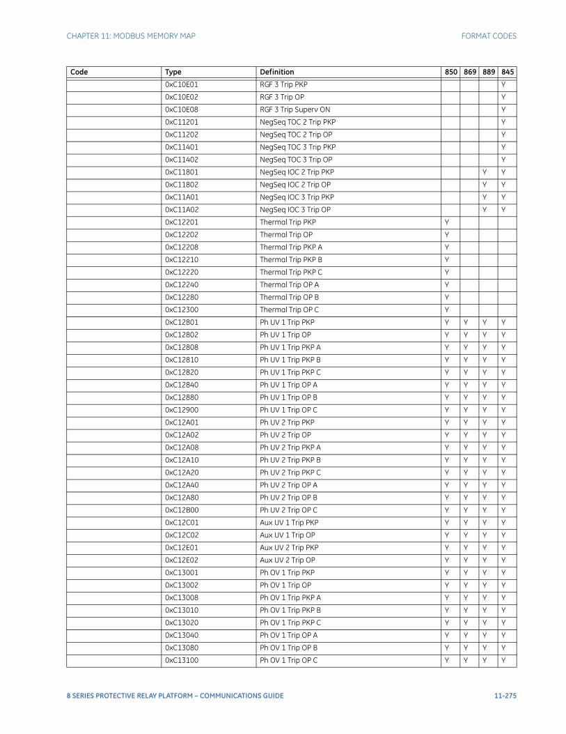
CHAPTER 11: MODBUS MEMORY MAP FORMAT CODES
0xC10E01 RGF 3 Trip PKP Y
0xC10E02 RGF 3 Trip OP Y
0xC10E08 RGF 3 Trip Superv ON Y
0xC11201 NegSeq TOC 2 Trip PKP Y
0xC11202 NegSeq TOC 2 Trip OP Y
0xC11401 NegSeq TOC 3 Trip PKP Y
0xC11402 NegSeq TOC 3 Trip OP Y
0xC11801 NegSeq IOC 2 Trip PKP Y Y
0xC11802 NegSeq IOC 2 Trip OP Y Y
0xC11A01 NegSeq IOC 3 Trip PKP Y Y
0xC11A02 NegSeq IOC 3 Trip OP Y Y
0xC12201 Thermal Trip PKP Y
0xC12202 Thermal Trip OP Y
0xC12208 Thermal Trip PKP A Y
0xC12210 Thermal Trip PKP B Y
0xC12220 Thermal Trip PKP C Y
0xC12240 Thermal Trip OP A Y
0xC12280 Thermal Trip OP B Y
0xC12300 Thermal Trip OP C Y
0xC12801 Ph UV 1 Trip PKP Y Y Y Y
0xC12802 Ph UV 1 Trip OP Y Y Y Y
0xC12808 Ph UV 1 Trip PKP A Y Y Y Y
0xC12810 Ph UV 1 Trip PKP B Y Y Y Y
0xC12820 Ph UV 1 Trip PKP C Y Y Y Y
0xC12840 Ph UV 1 Trip OP A Y Y Y Y
0xC12880 Ph UV 1 Trip OP B Y Y Y Y
0xC12900 Ph UV 1 Trip OP C Y Y Y Y
0xC12A01 Ph UV 2 Trip PKP Y Y Y Y
0xC12A02 Ph UV 2 Trip OP Y Y Y Y
0xC12A08 Ph UV 2 Trip PKP A Y Y Y Y
0xC12A10 Ph UV 2 Trip PKP B Y Y Y Y
0xC12A20 Ph UV 2 Trip PKP C Y Y Y Y
0xC12A40 Ph UV 2 Trip OP A Y Y Y Y
0xC12A80 Ph UV 2 Trip OP B Y Y Y Y
0xC12B00 Ph UV 2 Trip OP C Y Y Y Y
0xC12C01 Aux UV 1 Trip PKP Y Y Y Y
0xC12C02 Aux UV 1 Trip OP Y Y Y Y
0xC12E01 Aux UV 2 Trip PKP Y Y Y Y
0xC12E02 Aux UV 2 Trip OP Y Y Y Y
0xC13001 Ph OV 1 Trip PKP Y Y Y Y
0xC13002 Ph OV 1 Trip OP Y Y Y Y
0xC13008 Ph OV 1 Trip PKP A Y Y Y Y
0xC13010 Ph OV 1 Trip PKP B Y Y Y Y
0xC13020 Ph OV 1 Trip PKP C Y Y Y Y
0xC13040 Ph OV 1 Trip OP A Y Y Y Y
0xC13080 Ph OV 1 Trip OP B Y Y Y Y
0xC13100 Ph OV 1 Trip OP C Y Y Y Y
Code Type Definition 850 869 889 845
8 SERIES PROTECTIVE RELAY PLATFORM – COMMUNICATIONS GUIDE 11-275
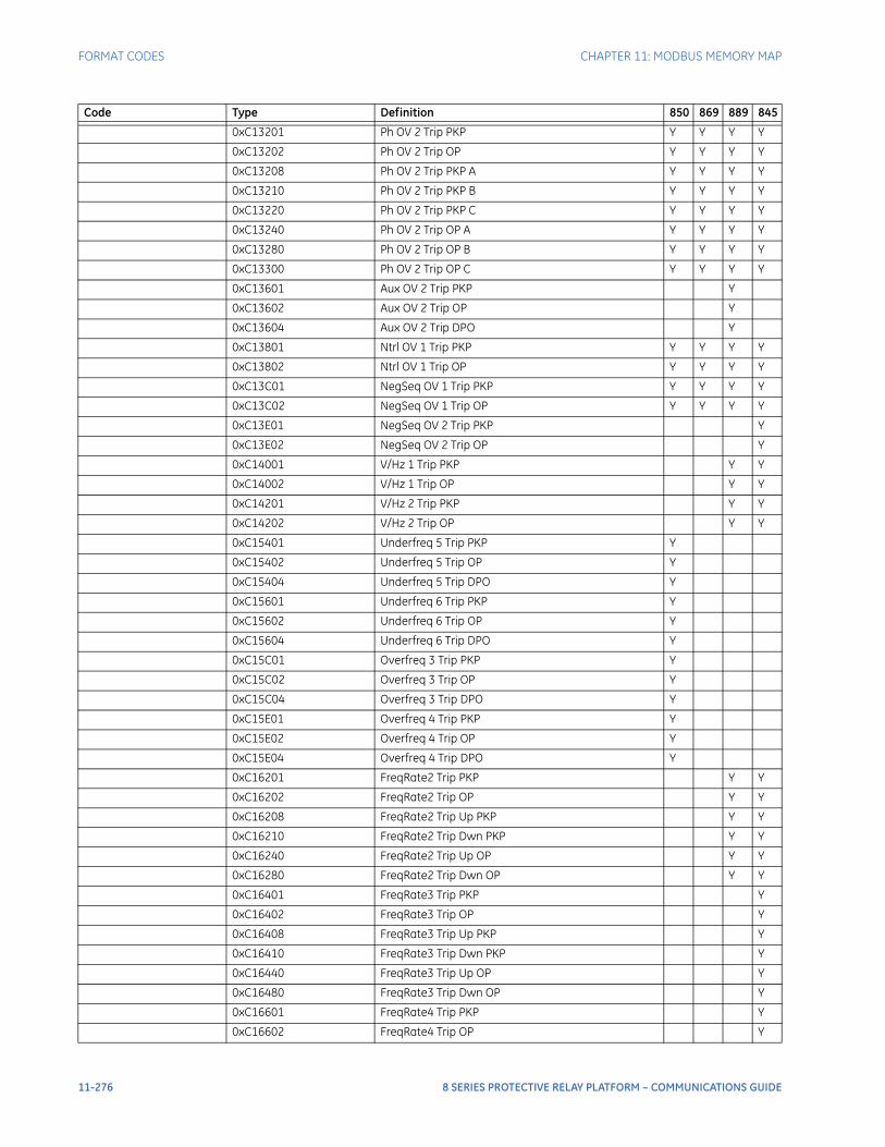
FORMAT CODES CHAPTER 11: MODBUS MEMORY MAP
0xC13201 Ph OV 2 Trip PKP Y Y Y Y
0xC13202 Ph OV 2 Trip OP Y Y Y Y
0xC13208 Ph OV 2 Trip PKP A Y Y Y Y
0xC13210 Ph OV 2 Trip PKP B Y Y Y Y
0xC13220 Ph OV 2 Trip PKP C Y Y Y Y
0xC13240 Ph OV 2 Trip OP A Y Y Y Y
0xC13280 Ph OV 2 Trip OP B Y Y Y Y
0xC13300 Ph OV 2 Trip OP C Y Y Y Y
0xC13601 Aux OV 2 Trip PKP Y
0xC13602 Aux OV 2 Trip OP Y
0xC13604 Aux OV 2 Trip DPO Y
0xC13801 Ntrl OV 1 Trip PKP Y Y Y Y
0xC13802 Ntrl OV 1 Trip OP Y Y Y Y
0xC13C01 NegSeq OV 1 Trip PKP Y Y Y Y
0xC13C02 NegSeq OV 1 Trip OP Y Y Y Y
0xC13E01 NegSeq OV 2 Trip PKP Y
0xC13E02 NegSeq OV 2 Trip OP Y
0xC14001 V/Hz 1 Trip PKP Y Y
0xC14002 V/Hz 1 Trip OP Y Y
0xC14201 V/Hz 2 Trip PKP Y Y
0xC14202 V/Hz 2 Trip OP Y Y
0xC15401 Underfreq 5 Trip PKP Y
0xC15402 Underfreq 5 Trip OP Y
0xC15404 Underfreq 5 Trip DPO Y
0xC15601 Underfreq 6 Trip PKP Y
0xC15602 Underfreq 6 Trip OP Y
0xC15604 Underfreq 6 Trip DPO Y
0xC15C01 Overfreq 3 Trip PKP Y
0xC15C02 Overfreq 3 Trip OP Y
0xC15C04 Overfreq 3 Trip DPO Y
0xC15E01 Overfreq 4 Trip PKP Y
0xC15E02 Overfreq 4 Trip OP Y
0xC15E04 Overfreq 4 Trip DPO Y
0xC16201 FreqRate2 Trip PKP Y Y
0xC16202 FreqRate2 Trip OP Y Y
0xC16208 FreqRate2 Trip Up PKP Y Y
0xC16210 FreqRate2 Trip Dwn PKP Y Y
0xC16240 FreqRate2 Trip Up OP Y Y
0xC16280 FreqRate2 Trip Dwn OP Y Y
0xC16401 FreqRate3 Trip PKP Y
0xC16402 FreqRate3 Trip OP Y
0xC16408 FreqRate3 Trip Up PKP Y
0xC16410 FreqRate3 Trip Dwn PKP Y
0xC16440 FreqRate3 Trip Up OP Y
0xC16480 FreqRate3 Trip Dwn OP Y
0xC16601 FreqRate4 Trip PKP Y
0xC16602 FreqRate4 Trip OP Y
Code Type Definition 850 869 889 845
11-276 8 SERIES PROTECTIVE RELAY PLATFORM – COMMUNICATIONS GUIDE

CHAPTER 11: MODBUS MEMORY MAP FORMAT CODES
0xC16608 FreqRate4 Trip Up PKP Y
0xC16610 FreqRate4 Trip Dwn PKP Y
0xC16640 FreqRate4 Trip Up OP Y
0xC16680 FreqRate4 Trip Dwn OP Y
0xC16801 FreqRate5 Trip PKP Y
0xC16802 FreqRate5 Trip OP Y
0xC16808 FreqRate5 Trip Up PKP Y
0xC16810 FreqRate5 Trip Dwn PKP Y
0xC16840 FreqRate5 Trip Up OP Y
0xC16880 FreqRate5 Trip Dwn OP Y
0xC16A01 FreqRate6 Trip PKP Y
0xC16A02 FreqRate6 Trip OP Y
0xC16A08 FreqRate6 Trip Up PKP Y
0xC16A10 FreqRate6 Trip Dwn PKP Y
0xC16A40 FreqRate6 Trip Up OP Y
0xC16A80 FreqRate6 Trip Dwn OP Y
0xC20801 Trip Bus 1 Trip PKP Y Y Y Y
0xC20802 Trip Bus 1 Trip OP Y Y Y Y
0xC20A01 Trip Bus 2 Trip PKP Y Y Y Y
0xC20A02 Trip Bus 2 Trip OP Y Y Y Y
0xC20C01 Trip Bus 3 Trip PKP Y Y Y Y
0xC20C02 Trip Bus 3 Trip OP Y Y Y Y
0xC20E01 Trip Bus 4 Trip PKP Y Y Y Y
0xC20E02 Trip Bus 4 Trip OP Y Y Y Y
0xC21001 Trip Bus 5 Trip PKP Y Y Y Y
0xC21002 Trip Bus 5 Trip OP Y Y Y Y
0xC21201 Trip Bus 6 Trip PKP Y Y Y Y
0xC21202 Trip Bus 6 Trip OP Y Y Y Y
0xC21402 BF1 Trip OP Y Y Y Y
0xC21408 BF1 Trip Retrip Y Y Y Y
0xC21410 BF1 Trip Highset OP Y Y Y Y
0xC21420 BF1 Trip Lowset OP Y Y Y Y
0xC21440 BF1 52b Trip Superv OP Y Y Y Y
0xC27201 RTD 1 Trip PKP Y Y Y Y
0xC27202 RTD 1 Trip OP Y Y Y Y
0xC27240 RTD 1 Open Y Y Y Y
0xC27280 RTD 1 Shorted Y Y Y Y
0xC27401 RTD 2 Trip PKP Y Y Y Y
0xC27402 RTD 2 Trip OP Y Y Y Y
0xC27440 RTD 2 Open Y Y Y Y
0xC27480 RTD 2 Shorted Y Y Y Y
0xC27601 RTD 3 Trip PKP Y Y Y Y
0xC27602 RTD 3 Trip OP Y Y Y Y
0xC27640 RTD 3 Open Y Y Y Y
0xC27680 RTD 3 Shorted Y Y Y Y
0xC27801 RTD 4 Trip PKP Y Y Y Y
0xC27802 RTD 4 Trip OP Y Y Y Y
Code Type Definition 850 869 889 845
8 SERIES PROTECTIVE RELAY PLATFORM – COMMUNICATIONS GUIDE 11-277

FORMAT CODES CHAPTER 11: MODBUS MEMORY MAP
0xC27840 RTD 4 Open Y Y Y Y
0xC27880 RTD 4 Shorted Y Y Y Y
0xC27A01 RTD 5 Trip PKP Y Y Y Y
0xC27A02 RTD 5 Trip OP Y Y Y Y
0xC27A40 RTD 5 Open Y Y Y Y
0xC27A80 RTD 5 Shorted Y Y Y Y
0xC27C01 RTD 6 Trip PKP Y Y Y Y
0xC27C02 RTD 6 Trip OP Y Y Y Y
0xC27C40 RTD 6 Open Y Y Y Y
0xC27C80 RTD 6 Shorted Y Y Y Y
0xC27E01 RTD 7 Trip PKP Y Y Y Y
0xC27E02 RTD 7 Trip OP Y Y Y Y
0xC27E40 RTD 7 Open Y Y Y Y
0xC27E80 RTD 7 Shorted Y Y Y Y
0xC28001 RTD 8 Trip PKP Y Y Y Y
0xC28002 RTD 8 Trip OP Y Y Y Y
0xC28040 RTD 8 Open Y Y Y Y
0xC28080 RTD 8 Shorted Y Y Y Y
0xC28201 RTD 9 Trip PKP Y Y Y Y
0xC28202 RTD 9 Trip OP Y Y Y Y
0xC28240 RTD 9 Open Y Y Y Y
0xC28280 RTD 9 Shorted Y Y Y Y
0xC28401 RTD 10 Trip PKP Y Y Y Y
0xC28402 RTD 10 Trip OP Y Y Y Y
0xC28440 RTD 10 Open Y Y Y Y
0xC28480 RTD 10 Shorted Y Y Y Y
0xC28601 RTD 11 Trip PKP Y Y Y Y
0xC28602 RTD 11 Trip OP Y Y Y Y
0xC28640 RTD 11 Open Y Y Y Y
0xC28680 RTD 11 Shorted Y Y Y Y
0xC28801 RTD 12 Trip PKP Y Y Y Y
0xC28802 RTD 12 Trip OP Y Y Y Y
0xC28840 RTD 12 Open Y Y Y Y
0xC28880 RTD 12 Shorted Y Y Y Y
0xC28A01 RTD 13 Trip PKP Y Y Y Y
0xC28A02 RTD 13 Trip OP Y Y Y Y
0xC28A40 RTD 13 Open Y Y Y Y
0xC28A80 RTD 13 Shorted Y Y Y Y
0xC30201 Anlg Ip 1 Trip PKP Y Y Y Y
0xC30202 Anlg Ip 1 Trip OP Y Y Y Y
0xC30401 Anlg Ip 2 Trip PKP Y Y Y Y
0xC30402 Anlg Ip 2 Trip OP Y Y Y Y
0xC30601 Anlg Ip 3 Trip PKP Y Y Y Y
0xC30602 Anlg Ip 3 Trip OP Y Y Y Y
0xC30801 Anlg Ip 4 Trip PKP Y Y Y Y
0xC30802 Anlg Ip 4 Trip OP Y Y Y Y
0xC33601 Fast UF 1 Trip PKP Y
Code Type Definition 850 869 889 845
11-278 8 SERIES PROTECTIVE RELAY PLATFORM – COMMUNICATIONS GUIDE
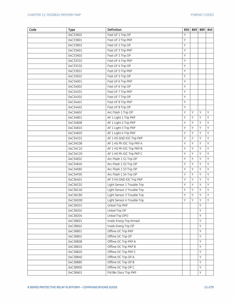
CHAPTER 11: MODBUS MEMORY MAP FORMAT CODES
0xC33602 Fast UF 1 Trip OP Y
0xC33801 Fast UF 2 Trip PKP Y
0xC33802 Fast UF 2 Trip OP Y
0xC33A01 Fast UF 3 Trip PKP Y
0xC33A02 Fast UF 3 Trip OP Y
0xC33C01 Fast UF 4 Trip PKP Y
0xC33C02 Fast UF 4 Trip OP Y
0xC33E01 Fast UF 5 Trip PKP Y
0xC33E02 Fast UF 5 Trip OP Y
0xC34001 Fast UF 6 Trip PKP Y
0xC34002 Fast UF 6 Trip OP Y
0xC34201 Fast UF 7 Trip PKP Y
0xC34202 Fast UF 7 Trip OP Y
0xC34401 Fast UF 8 Trip PKP Y
0xC34402 Fast UF 8 Trip OP Y
0xC34602 Arc Flash 1 Trip OP Y Y Y Y
0xC34801 AF 1 Light 1 Trip PKP Y Y Y Y
0xC34808 AF 1 Light 2 Trip PKP Y Y Y Y
0xC34810 AF 1 Light 3 Trip PKP Y Y Y Y
0xC34820 AF 1 Light 4 Trip PKP Y Y Y Y
0xC34C01 AF 1 HS GND IOC Trip PKP Y Y Y Y
0xC34C08 AF 1 HS Ph IOC Trip PKP A Y Y Y Y
0xC34C10 AF 1 HS Ph IOC Trip PKP B Y Y Y Y
0xC34C20 AF 1 HS Ph IOC Trip PKP C Y Y Y Y
0xC34E02 Arc Flash 1 S1 Trip OP Y Y Y Y
0xC34E40 Arc Flash 1 S2 Trip OP Y Y Y Y
0xC34E80 Arc Flash 1 S3 Trip OP Y Y Y Y
0xC34F00 Arc Flash 1 S4 Trip OP Y Y Y Y
0xC36401 AF 3 HS GND IOC Trip PKP Y Y Y Y
0xC36C02 Light Sensor 1 Trouble Trip Y Y Y Y
0xC36C40 Light Sensor 2 Trouble Trip Y Y Y Y
0xC36C80 Light Sensor 3 Trouble Trip Y Y Y Y
0xC36D00 Light Sensor 4 Trouble Trip Y Y Y Y
0xC38201 Unbal Trip PKP Y
0xC38202 Unbal Trip OP Y
0xC38204 Unbal Trip DPO Y
0xC38601 Inadv Energ Trip Armed Y
0xC38602 Inadv Energ Trip OP Y
0xC38801 Offline OC Trip PKP Y
0xC38802 Offline OC Trip OP Y
0xC38808 Offline OC Trip PKP A Y
0xC38810 Offline OC Trip PKP B Y
0xC38820 Offline OC Trip PKP C Y
0xC38840 Offline OC Trip OP A Y
0xC38880 Offline OC Trip OP B Y
0xC38900 Offline OC Trip OP C Y
0xC38A01 Fld Bkr Discr Trip PKP Y
Code Type Definition 850 869 889 845
8 SERIES PROTECTIVE RELAY PLATFORM – COMMUNICATIONS GUIDE 11-279
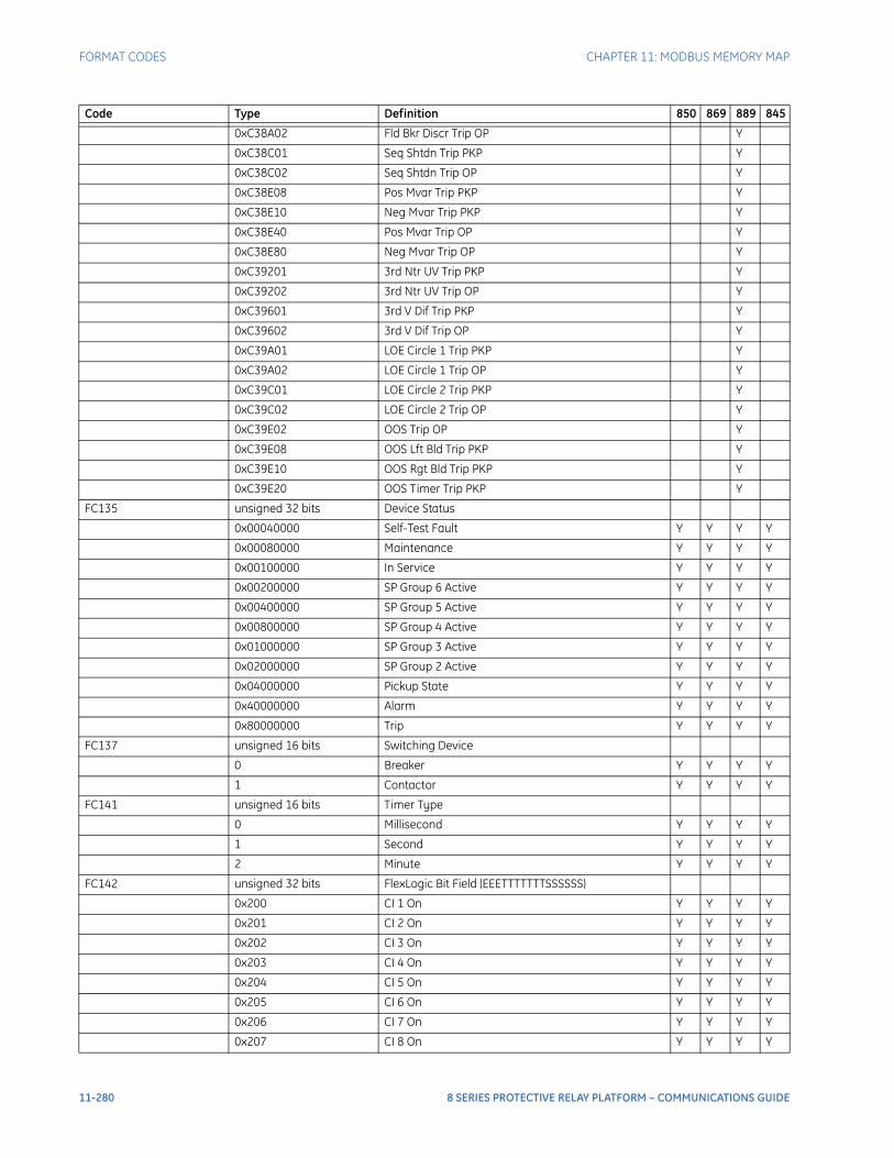
FORMAT CODES CHAPTER 11: MODBUS MEMORY MAP
0xC38A02 Fld Bkr Discr Trip OP Y
0xC38C01 Seq Shtdn Trip PKP Y
0xC38C02 Seq Shtdn Trip OP Y
0xC38E08 Pos Mvar Trip PKP Y
0xC38E10 Neg Mvar Trip PKP Y
0xC38E40 Pos Mvar Trip OP Y
0xC38E80 Neg Mvar Trip OP Y
0xC39201 3rd Ntr UV Trip PKP Y
0xC39202 3rd Ntr UV Trip OP Y
0xC39601 3rd V Dif Trip PKP Y
0xC39602 3rd V Dif Trip OP Y
0xC39A01 LOE Circle 1 Trip PKP Y
0xC39A02 LOE Circle 1 Trip OP Y
0xC39C01 LOE Circle 2 Trip PKP Y
0xC39C02 LOE Circle 2 Trip OP Y
0xC39E02 OOS Trip OP Y
0xC39E08 OOS Lft Bld Trip PKP Y
0xC39E10 OOS Rgt Bld Trip PKP Y
0xC39E20 OOS Timer Trip PKP Y
FC135 unsigned 32 bits Device Status
0x00040000 Self-Test Fault Y Y Y Y
0x00080000 Maintenance Y Y Y Y
0x00100000 In Service Y Y Y Y
0x00200000 SP Group 6 Active Y Y Y Y
0x00400000 SP Group 5 Active Y Y Y Y
0x00800000 SP Group 4 Active Y Y Y Y
0x01000000 SP Group 3 Active Y Y Y Y
0x02000000 SP Group 2 Active Y Y Y Y
0x04000000 Pickup State Y Y Y Y
0x40000000 Alarm Y Y Y Y
0x80000000 Trip Y Y Y Y
FC137 unsigned 16 bits Switching Device
0 Breaker Y Y Y Y
1 Contactor Y Y Y Y
FC141 unsigned 16 bits Timer Type
0 Millisecond Y Y Y Y
1 Second Y Y Y Y
2 Minute Y Y Y Y
FC142 unsigned 32 bits FlexLogic Bit Field (EEETTTTTTTSSSSSS)
0x200 CI 1 On Y Y Y Y
0x201 CI 2 On Y Y Y Y
0x202 CI 3 On Y Y Y Y
0x203 CI 4 On Y Y Y Y
0x204 CI 5 On Y Y Y Y
0x205 CI 6 On Y Y Y Y
0x206 CI 7 On Y Y Y Y
0x207 CI 8 On Y Y Y Y
Code Type Definition 850 869 889 845
11-280 8 SERIES PROTECTIVE RELAY PLATFORM – COMMUNICATIONS GUIDE

CHAPTER 11: MODBUS MEMORY MAP FORMAT CODES
0x208 CI 9 On Y Y Y Y
0x209 CI 10 On Y Y Y Y
0x20A CI 11 On Y Y Y Y
0x20B CI 12 On Y Y Y Y
0x20C CI 13 On Y Y Y Y
0x20D CI 14 On Y Y Y Y
0x20E CI 15 On Y Y Y Y
0x20F CI 16 On Y Y Y Y
0x210 CI 17 On Y Y Y Y
0x211 CI 18 On Y Y Y Y
0x212 CI 19 On Y Y Y Y
0x213 CI 20 On Y Y Y Y
0x214 CI 21 On Y Y Y Y
0x215 CI 22 On Y Y Y Y
0x216 CI 23 On Y Y Y Y
0x217 CI 24 On Y Y Y Y
0x218 CI 25 On Y Y Y Y
0x219 CI 26 On Y Y Y Y
0x21A CI 27 On Y Y Y Y
0x21B CI 28 On Y Y Y Y
0x21C CI 29 On Y Y Y Y
0x21D CI 30 On Y Y Y Y
0x21E CI 31 On Y Y Y Y
0x21F CI 32 On Y Y Y Y
0x220 CI 33 On Y Y Y Y
0x221 CI 34 On Y Y Y Y
0x222 CI 35 On Y Y Y Y
0x223 CI 36 On Y Y Y Y
0x224 CI 37 On Y Y Y Y
0x225 CI 38 On Y Y Y Y
0x226 CI 39 On Y Y Y Y
0x227 CI 40 On Y Y Y Y
0x228 CI 41 On Y Y Y Y
0x229 CI 42 On Y Y Y Y
0x22A CI 43 On Y Y Y Y
0x22B CI 44 On Y Y Y Y
0x22C CI 45 On Y Y Y Y
0x22D CI 46 On Y Y Y Y
0x22E CI 47 On Y Y Y Y
0x22F CI 48 On Y Y Y Y
0x230 CI 49 On Y Y Y Y
0x231 CI 50 On Y Y Y Y
0x232 CI 51 On Y Y Y Y
0x233 CI 52 On Y Y Y Y
0x234 CI 53 On Y Y Y Y
0x235 CI 54 On Y Y Y Y
0x236 CI 55 On Y Y Y Y
Code Type Definition 850 869 889 845
8 SERIES PROTECTIVE RELAY PLATFORM – COMMUNICATIONS GUIDE 11-281
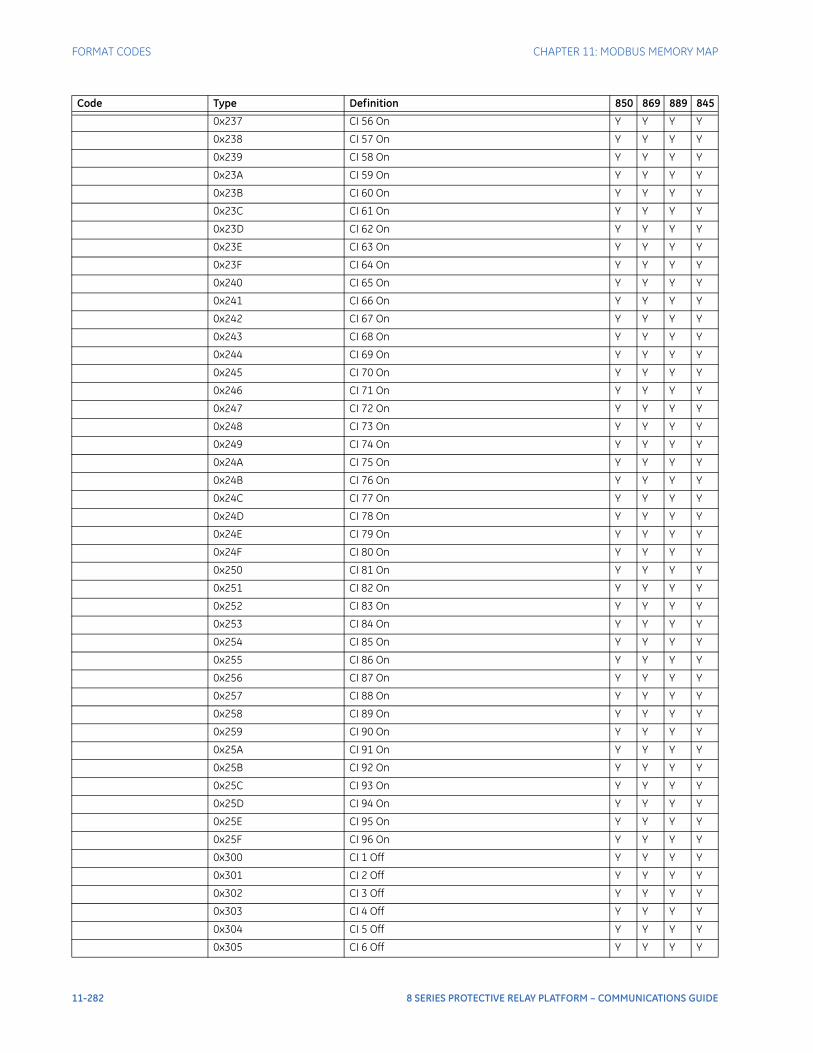
FORMAT CODES CHAPTER 11: MODBUS MEMORY MAP
0x237 CI 56 On Y Y Y Y
0x238 CI 57 On Y Y Y Y
0x239 CI 58 On Y Y Y Y
0x23A CI 59 On Y Y Y Y
0x23B CI 60 On Y Y Y Y
0x23C CI 61 On Y Y Y Y
0x23D CI 62 On Y Y Y Y
0x23E CI 63 On Y Y Y Y
0x23F CI 64 On Y Y Y Y
0x240 CI 65 On Y Y Y Y
0x241 CI 66 On Y Y Y Y
0x242 CI 67 On Y Y Y Y
0x243 CI 68 On Y Y Y Y
0x244 CI 69 On Y Y Y Y
0x245 CI 70 On Y Y Y Y
0x246 CI 71 On Y Y Y Y
0x247 CI 72 On Y Y Y Y
0x248 CI 73 On Y Y Y Y
0x249 CI 74 On Y Y Y Y
0x24A CI 75 On Y Y Y Y
0x24B CI 76 On Y Y Y Y
0x24C CI 77 On Y Y Y Y
0x24D CI 78 On Y Y Y Y
0x24E CI 79 On Y Y Y Y
0x24F CI 80 On Y Y Y Y
0x250 CI 81 On Y Y Y Y
0x251 CI 82 On Y Y Y Y
0x252 CI 83 On Y Y Y Y
0x253 CI 84 On Y Y Y Y
0x254 CI 85 On Y Y Y Y
0x255 CI 86 On Y Y Y Y
0x256 CI 87 On Y Y Y Y
0x257 CI 88 On Y Y Y Y
0x258 CI 89 On Y Y Y Y
0x259 CI 90 On Y Y Y Y
0x25A CI 91 On Y Y Y Y
0x25B CI 92 On Y Y Y Y
0x25C CI 93 On Y Y Y Y
0x25D CI 94 On Y Y Y Y
0x25E CI 95 On Y Y Y Y
0x25F CI 96 On Y Y Y Y
0x300 CI 1 Off Y Y Y Y
0x301 CI 2 Off Y Y Y Y
0x302 CI 3 Off Y Y Y Y
0x303 CI 4 Off Y Y Y Y
0x304 CI 5 Off Y Y Y Y
0x305 CI 6 Off Y Y Y Y
Code Type Definition 850 869 889 845
11-282 8 SERIES PROTECTIVE RELAY PLATFORM – COMMUNICATIONS GUIDE
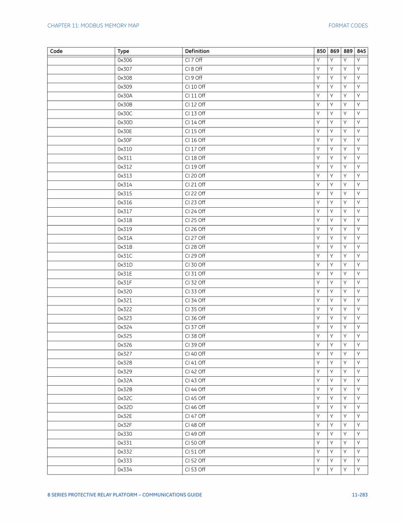
CHAPTER 11: MODBUS MEMORY MAP FORMAT CODES
0x306 CI 7 Off Y Y Y Y
0x307 CI 8 Off Y Y Y Y
0x308 CI 9 Off Y Y Y Y
0x309 CI 10 Off Y Y Y Y
0x30A CI 11 Off Y Y Y Y
0x30B CI 12 Off Y Y Y Y
0x30C CI 13 Off Y Y Y Y
0x30D CI 14 Off Y Y Y Y
0x30E CI 15 Off Y Y Y Y
0x30F CI 16 Off Y Y Y Y
0x310 CI 17 Off Y Y Y Y
0x311 CI 18 Off Y Y Y Y
0x312 CI 19 Off Y Y Y Y
0x313 CI 20 Off Y Y Y Y
0x314 CI 21 Off Y Y Y Y
0x315 CI 22 Off Y Y Y Y
0x316 CI 23 Off Y Y Y Y
0x317 CI 24 Off Y Y Y Y
0x318 CI 25 Off Y Y Y Y
0x319 CI 26 Off Y Y Y Y
0x31A CI 27 Off Y Y Y Y
0x31B CI 28 Off Y Y Y Y
0x31C CI 29 Off Y Y Y Y
0x31D CI 30 Off Y Y Y Y
0x31E CI 31 Off Y Y Y Y
0x31F CI 32 Off Y Y Y Y
0x320 CI 33 Off Y Y Y Y
0x321 CI 34 Off Y Y Y Y
0x322 CI 35 Off Y Y Y Y
0x323 CI 36 Off Y Y Y Y
0x324 CI 37 Off Y Y Y Y
0x325 CI 38 Off Y Y Y Y
0x326 CI 39 Off Y Y Y Y
0x327 CI 40 Off Y Y Y Y
0x328 CI 41 Off Y Y Y Y
0x329 CI 42 Off Y Y Y Y
0x32A CI 43 Off Y Y Y Y
0x32B CI 44 Off Y Y Y Y
0x32C CI 45 Off Y Y Y Y
0x32D CI 46 Off Y Y Y Y
0x32E CI 47 Off Y Y Y Y
0x32F CI 48 Off Y Y Y Y
0x330 CI 49 Off Y Y Y Y
0x331 CI 50 Off Y Y Y Y
0x332 CI 51 Off Y Y Y Y
0x333 CI 52 Off Y Y Y Y
0x334 CI 53 Off Y Y Y Y
Code Type Definition 850 869 889 845
8 SERIES PROTECTIVE RELAY PLATFORM – COMMUNICATIONS GUIDE 11-283

FORMAT CODES CHAPTER 11: MODBUS MEMORY MAP
0x335 CI 54 Off Y Y Y Y
0x336 CI 55 Off Y Y Y Y
0x337 CI 56 Off Y Y Y Y
0x338 CI 57 Off Y Y Y Y
0x339 CI 58 Off Y Y Y Y
0x33A CI 59 Off Y Y Y Y
0x33B CI 60 Off Y Y Y Y
0x33C CI 61 Off Y Y Y Y
0x33D CI 62 Off Y Y Y Y
0x33E CI 63 Off Y Y Y Y
0x33F CI 64 Off Y Y Y Y
0x340 CI 65 Off Y Y Y Y
0x341 CI 66 Off Y Y Y Y
0x342 CI 67 Off Y Y Y Y
0x343 CI 68 Off Y Y Y Y
0x344 CI 69 Off Y Y Y Y
0x345 CI 70 Off Y Y Y Y
0x346 CI 71 Off Y Y Y Y
0x347 CI 72 Off Y Y Y Y
0x348 CI 73 Off Y Y Y Y
0x349 CI 74 Off Y Y Y Y
0x34A CI 75 Off Y Y Y Y
0x34B CI 76 Off Y Y Y Y
0x34C CI 77 Off Y Y Y Y
0x34D CI 78 Off Y Y Y Y
0x34E CI 79 Off Y Y Y Y
0x34F CI 80 Off Y Y Y Y
0x350 CI 81 Off Y Y Y Y
0x351 CI 82 Off Y Y Y Y
0x352 CI 83 Off Y Y Y Y
0x353 CI 84 Off Y Y Y Y
0x354 CI 85 Off Y Y Y Y
0x355 CI 86 Off Y Y Y Y
0x356 CI 87 Off Y Y Y Y
0x357 CI 88 Off Y Y Y Y
0x358 CI 89 Off Y Y Y Y
0x359 CI 90 Off Y Y Y Y
0x35A CI 91 Off Y Y Y Y
0x35B CI 92 Off Y Y Y Y
0x35C CI 93 Off Y Y Y Y
0x35D CI 94 Off Y Y Y Y
0x35E CI 95 Off Y Y Y Y
0x35F CI 96 Off Y Y Y Y
0x400 VI 1 On Y Y Y Y
0x401 VI 2 On Y Y Y Y
0x402 VI 3 On Y Y Y Y
0x403 VI 4 On Y Y Y Y
Code Type Definition 850 869 889 845
11-284 8 SERIES PROTECTIVE RELAY PLATFORM – COMMUNICATIONS GUIDE
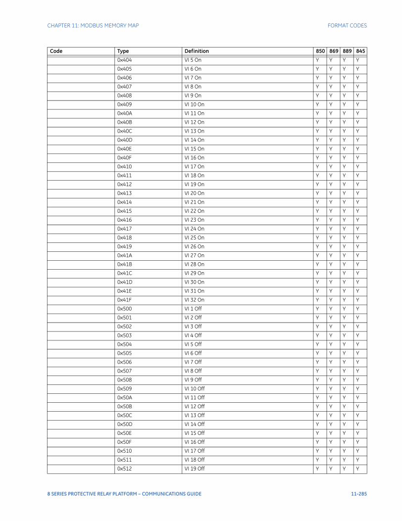
CHAPTER 11: MODBUS MEMORY MAP FORMAT CODES
0x404 VI 5 On Y Y Y Y
0x405 VI 6 On Y Y Y Y
0x406 VI 7 On Y Y Y Y
0x407 VI 8 On Y Y Y Y
0x408 VI 9 On Y Y Y Y
0x409 VI 10 On Y Y Y Y
0x40A VI 11 On Y Y Y Y
0x40B VI 12 On Y Y Y Y
0x40C VI 13 On Y Y Y Y
0x40D VI 14 On Y Y Y Y
0x40E VI 15 On Y Y Y Y
0x40F VI 16 On Y Y Y Y
0x410 VI 17 On Y Y Y Y
0x411 VI 18 On Y Y Y Y
0x412 VI 19 On Y Y Y Y
0x413 VI 20 On Y Y Y Y
0x414 VI 21 On Y Y Y Y
0x415 VI 22 On Y Y Y Y
0x416 VI 23 On Y Y Y Y
0x417 VI 24 On Y Y Y Y
0x418 VI 25 On Y Y Y Y
0x419 VI 26 On Y Y Y Y
0x41A VI 27 On Y Y Y Y
0x41B VI 28 On Y Y Y Y
0x41C VI 29 On Y Y Y Y
0x41D VI 30 On Y Y Y Y
0x41E VI 31 On Y Y Y Y
0x41F VI 32 On Y Y Y Y
0x500 VI 1 Off Y Y Y Y
0x501 VI 2 Off Y Y Y Y
0x502 VI 3 Off Y Y Y Y
0x503 VI 4 Off Y Y Y Y
0x504 VI 5 Off Y Y Y Y
0x505 VI 6 Off Y Y Y Y
0x506 VI 7 Off Y Y Y Y
0x507 VI 8 Off Y Y Y Y
0x508 VI 9 Off Y Y Y Y
0x509 VI 10 Off Y Y Y Y
0x50A VI 11 Off Y Y Y Y
0x50B VI 12 Off Y Y Y Y
0x50C VI 13 Off Y Y Y Y
0x50D VI 14 Off Y Y Y Y
0x50E VI 15 Off Y Y Y Y
0x50F VI 16 Off Y Y Y Y
0x510 VI 17 Off Y Y Y Y
0x511 VI 18 Off Y Y Y Y
0x512 VI 19 Off Y Y Y Y
Code Type Definition 850 869 889 845
8 SERIES PROTECTIVE RELAY PLATFORM – COMMUNICATIONS GUIDE 11-285
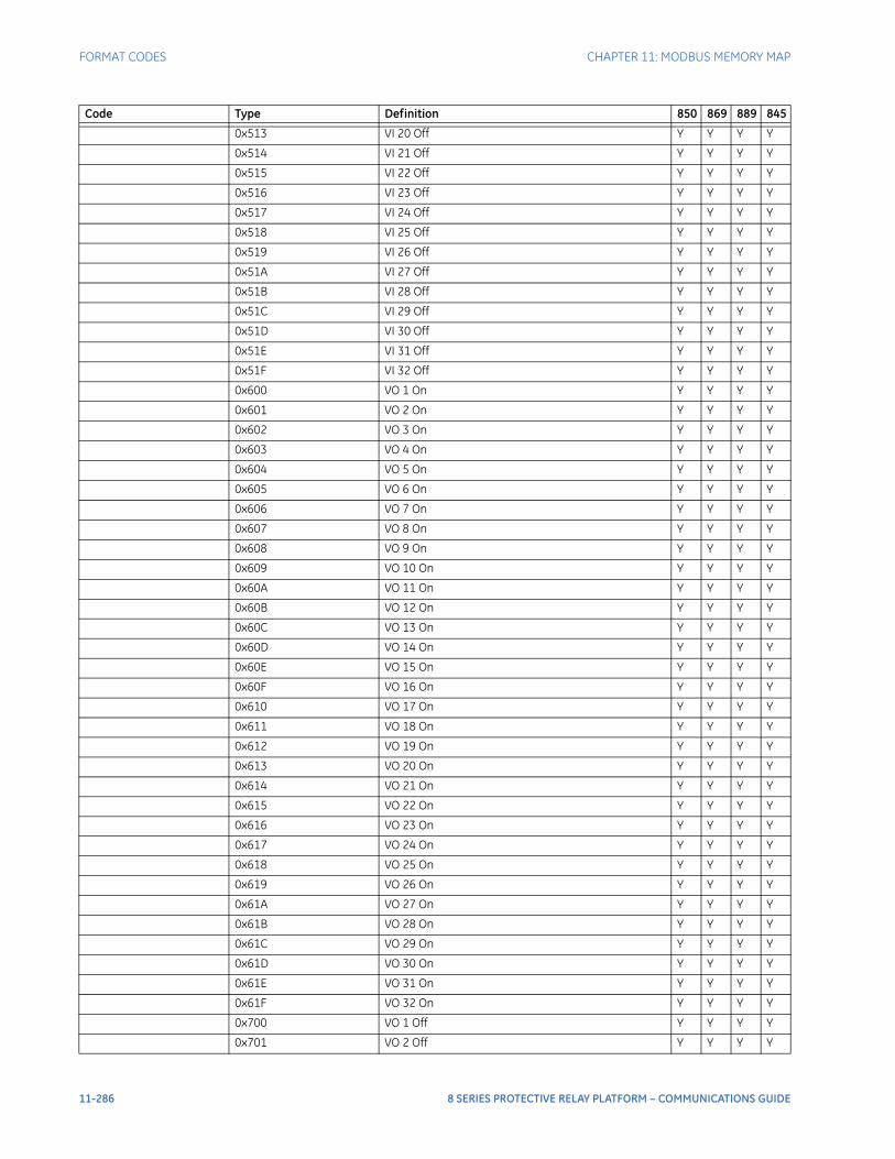
FORMAT CODES CHAPTER 11: MODBUS MEMORY MAP
0x513 VI 20 Off Y Y Y Y
0x514 VI 21 Off Y Y Y Y
0x515 VI 22 Off Y Y Y Y
0x516 VI 23 Off Y Y Y Y
0x517 VI 24 Off Y Y Y Y
0x518 VI 25 Off Y Y Y Y
0x519 VI 26 Off Y Y Y Y
0x51A VI 27 Off Y Y Y Y
0x51B VI 28 Off Y Y Y Y
0x51C VI 29 Off Y Y Y Y
0x51D VI 30 Off Y Y Y Y
0x51E VI 31 Off Y Y Y Y
0x51F VI 32 Off Y Y Y Y
0x600 VO 1 On Y Y Y Y
0x601 VO 2 On Y Y Y Y
0x602 VO 3 On Y Y Y Y
0x603 VO 4 On Y Y Y Y
0x604 VO 5 On Y Y Y Y
0x605 VO 6 On Y Y Y Y
0x606 VO 7 On Y Y Y Y
0x607 VO 8 On Y Y Y Y
0x608 VO 9 On Y Y Y Y
0x609 VO 10 On Y Y Y Y
0x60A VO 11 On Y Y Y Y
0x60B VO 12 On Y Y Y Y
0x60C VO 13 On Y Y Y Y
0x60D VO 14 On Y Y Y Y
0x60E VO 15 On Y Y Y Y
0x60F VO 16 On Y Y Y Y
0x610 VO 17 On Y Y Y Y
0x611 VO 18 On Y Y Y Y
0x612 VO 19 On Y Y Y Y
0x613 VO 20 On Y Y Y Y
0x614 VO 21 On Y Y Y Y
0x615 VO 22 On Y Y Y Y
0x616 VO 23 On Y Y Y Y
0x617 VO 24 On Y Y Y Y
0x618 VO 25 On Y Y Y Y
0x619 VO 26 On Y Y Y Y
0x61A VO 27 On Y Y Y Y
0x61B VO 28 On Y Y Y Y
0x61C VO 29 On Y Y Y Y
0x61D VO 30 On Y Y Y Y
0x61E VO 31 On Y Y Y Y
0x61F VO 32 On Y Y Y Y
0x700 VO 1 Off Y Y Y Y
0x701 VO 2 Off Y Y Y Y
Code Type Definition 850 869 889 845
11-286 8 SERIES PROTECTIVE RELAY PLATFORM – COMMUNICATIONS GUIDE
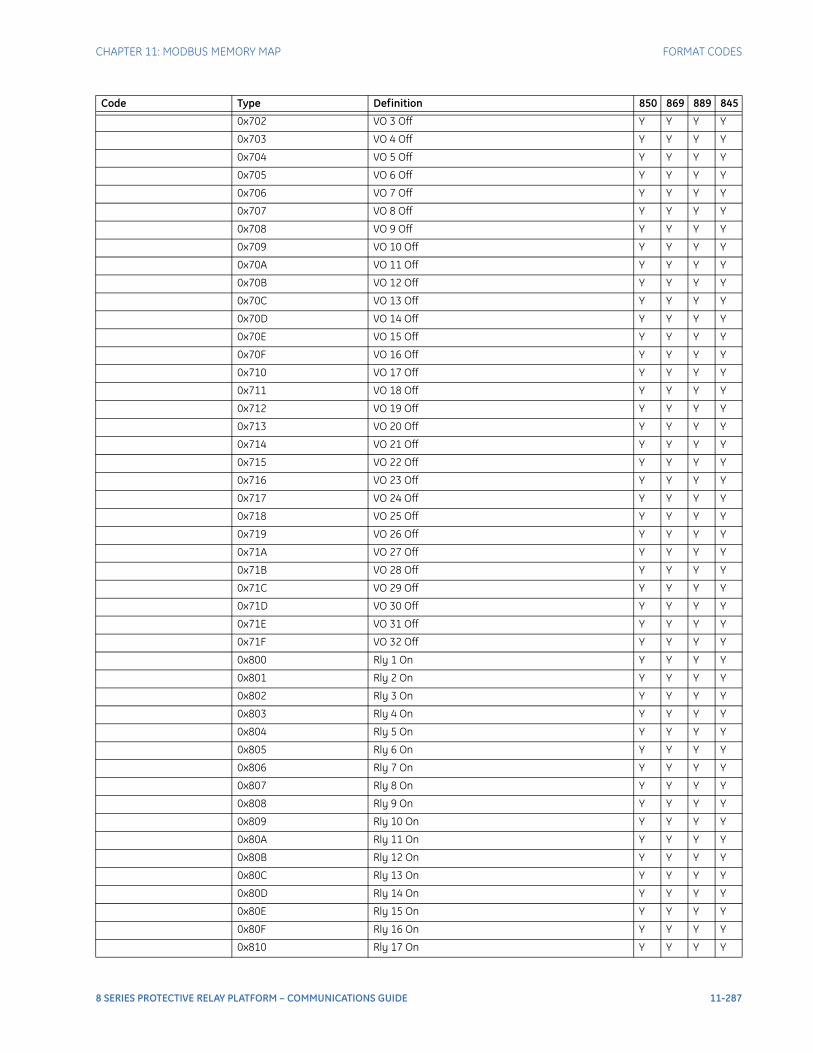
CHAPTER 11: MODBUS MEMORY MAP FORMAT CODES
0x702 VO 3 Off Y Y Y Y
0x703 VO 4 Off Y Y Y Y
0x704 VO 5 Off Y Y Y Y
0x705 VO 6 Off Y Y Y Y
0x706 VO 7 Off Y Y Y Y
0x707 VO 8 Off Y Y Y Y
0x708 VO 9 Off Y Y Y Y
0x709 VO 10 Off Y Y Y Y
0x70A VO 11 Off Y Y Y Y
0x70B VO 12 Off Y Y Y Y
0x70C VO 13 Off Y Y Y Y
0x70D VO 14 Off Y Y Y Y
0x70E VO 15 Off Y Y Y Y
0x70F VO 16 Off Y Y Y Y
0x710 VO 17 Off Y Y Y Y
0x711 VO 18 Off Y Y Y Y
0x712 VO 19 Off Y Y Y Y
0x713 VO 20 Off Y Y Y Y
0x714 VO 21 Off Y Y Y Y
0x715 VO 22 Off Y Y Y Y
0x716 VO 23 Off Y Y Y Y
0x717 VO 24 Off Y Y Y Y
0x718 VO 25 Off Y Y Y Y
0x719 VO 26 Off Y Y Y Y
0x71A VO 27 Off Y Y Y Y
0x71B VO 28 Off Y Y Y Y
0x71C VO 29 Off Y Y Y Y
0x71D VO 30 Off Y Y Y Y
0x71E VO 31 Off Y Y Y Y
0x71F VO 32 Off Y Y Y Y
0x800 Rly 1 On Y Y Y Y
0x801 Rly 2 On Y Y Y Y
0x802 Rly 3 On Y Y Y Y
0x803 Rly 4 On Y Y Y Y
0x804 Rly 5 On Y Y Y Y
0x805 Rly 6 On Y Y Y Y
0x806 Rly 7 On Y Y Y Y
0x807 Rly 8 On Y Y Y Y
0x808 Rly 9 On Y Y Y Y
0x809 Rly 10 On Y Y Y Y
0x80A Rly 11 On Y Y Y Y
0x80B Rly 12 On Y Y Y Y
0x80C Rly 13 On Y Y Y Y
0x80D Rly 14 On Y Y Y Y
0x80E Rly 15 On Y Y Y Y
0x80F Rly 16 On Y Y Y Y
0x810 Rly 17 On Y Y Y Y
Code Type Definition 850 869 889 845
8 SERIES PROTECTIVE RELAY PLATFORM – COMMUNICATIONS GUIDE 11-287
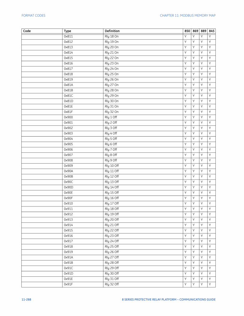
FORMAT CODES CHAPTER 11: MODBUS MEMORY MAP
0x811 Rly 18 On Y Y Y Y
0x812 Rly 19 On Y Y Y Y
0x813 Rly 20 On Y Y Y Y
0x814 Rly 21 On Y Y Y Y
0x815 Rly 22 On Y Y Y Y
0x816 Rly 23 On Y Y Y Y
0x817 Rly 24 On Y Y Y Y
0x818 Rly 25 On Y Y Y Y
0x819 Rly 26 On Y Y Y Y
0x81A Rly 27 On Y Y Y Y
0x81B Rly 28 On Y Y Y Y
0x81C Rly 29 On Y Y Y Y
0x81D Rly 30 On Y Y Y Y
0x81E Rly 31 On Y Y Y Y
0x81F Rly 32 On Y Y Y Y
0x900 Rly 1 Off Y Y Y Y
0x901 Rly 2 Off Y Y Y Y
0x902 Rly 3 Off Y Y Y Y
0x903 Rly 4 Off Y Y Y Y
0x904 Rly 5 Off Y Y Y Y
0x905 Rly 6 Off Y Y Y Y
0x906 Rly 7 Off Y Y Y Y
0x907 Rly 8 Off Y Y Y Y
0x908 Rly 9 Off Y Y Y Y
0x909 Rly 10 Off Y Y Y Y
0x90A Rly 11 Off Y Y Y Y
0x90B Rly 12 Off Y Y Y Y
0x90C Rly 13 Off Y Y Y Y
0x90D Rly 14 Off Y Y Y Y
0x90E Rly 15 Off Y Y Y Y
0x90F Rly 16 Off Y Y Y Y
0x910 Rly 17 Off Y Y Y Y
0x911 Rly 18 Off Y Y Y Y
0x912 Rly 19 Off Y Y Y Y
0x913 Rly 20 Off Y Y Y Y
0x914 Rly 21 Off Y Y Y Y
0x915 Rly 22 Off Y Y Y Y
0x916 Rly 23 Off Y Y Y Y
0x917 Rly 24 Off Y Y Y Y
0x918 Rly 25 Off Y Y Y Y
0x919 Rly 26 Off Y Y Y Y
0x91A Rly 27 Off Y Y Y Y
0x91B Rly 28 Off Y Y Y Y
0x91C Rly 29 Off Y Y Y Y
0x91D Rly 30 Off Y Y Y Y
0x91E Rly 31 Off Y Y Y Y
0x91F Rly 32 Off Y Y Y Y
Code Type Definition 850 869 889 845
11-288 8 SERIES PROTECTIVE RELAY PLATFORM – COMMUNICATIONS GUIDE
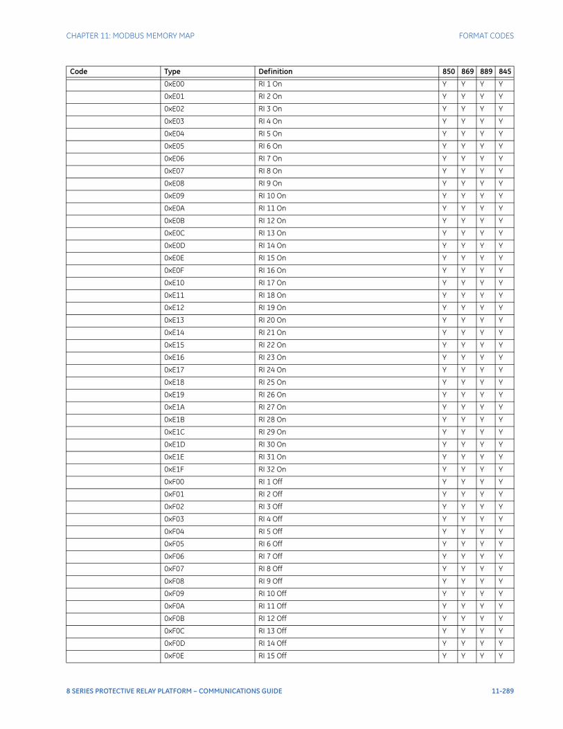
CHAPTER 11: MODBUS MEMORY MAP FORMAT CODES
0xE00 RI 1 On Y Y Y Y
0xE01 RI 2 On Y Y Y Y
0xE02 RI 3 On Y Y Y Y
0xE03 RI 4 On Y Y Y Y
0xE04 RI 5 On Y Y Y Y
0xE05 RI 6 On Y Y Y Y
0xE06 RI 7 On Y Y Y Y
0xE07 RI 8 On Y Y Y Y
0xE08 RI 9 On Y Y Y Y
0xE09 RI 10 On Y Y Y Y
0xE0A RI 11 On Y Y Y Y
0xE0B RI 12 On Y Y Y Y
0xE0C RI 13 On Y Y Y Y
0xE0D RI 14 On Y Y Y Y
0xE0E RI 15 On Y Y Y Y
0xE0F RI 16 On Y Y Y Y
0xE10 RI 17 On Y Y Y Y
0xE11 RI 18 On Y Y Y Y
0xE12 RI 19 On Y Y Y Y
0xE13 RI 20 On Y Y Y Y
0xE14 RI 21 On Y Y Y Y
0xE15 RI 22 On Y Y Y Y
0xE16 RI 23 On Y Y Y Y
0xE17 RI 24 On Y Y Y Y
0xE18 RI 25 On Y Y Y Y
0xE19 RI 26 On Y Y Y Y
0xE1A RI 27 On Y Y Y Y
0xE1B RI 28 On Y Y Y Y
0xE1C RI 29 On Y Y Y Y
0xE1D RI 30 On Y Y Y Y
0xE1E RI 31 On Y Y Y Y
0xE1F RI 32 On Y Y Y Y
0xF00 RI 1 Off Y Y Y Y
0xF01 RI 2 Off Y Y Y Y
0xF02 RI 3 Off Y Y Y Y
0xF03 RI 4 Off Y Y Y Y
0xF04 RI 5 Off Y Y Y Y
0xF05 RI 6 Off Y Y Y Y
0xF06 RI 7 Off Y Y Y Y
0xF07 RI 8 Off Y Y Y Y
0xF08 RI 9 Off Y Y Y Y
0xF09 RI 10 Off Y Y Y Y
0xF0A RI 11 Off Y Y Y Y
0xF0B RI 12 Off Y Y Y Y
0xF0C RI 13 Off Y Y Y Y
0xF0D RI 14 Off Y Y Y Y
0xF0E RI 15 Off Y Y Y Y
Code Type Definition 850 869 889 845
8 SERIES PROTECTIVE RELAY PLATFORM – COMMUNICATIONS GUIDE 11-289
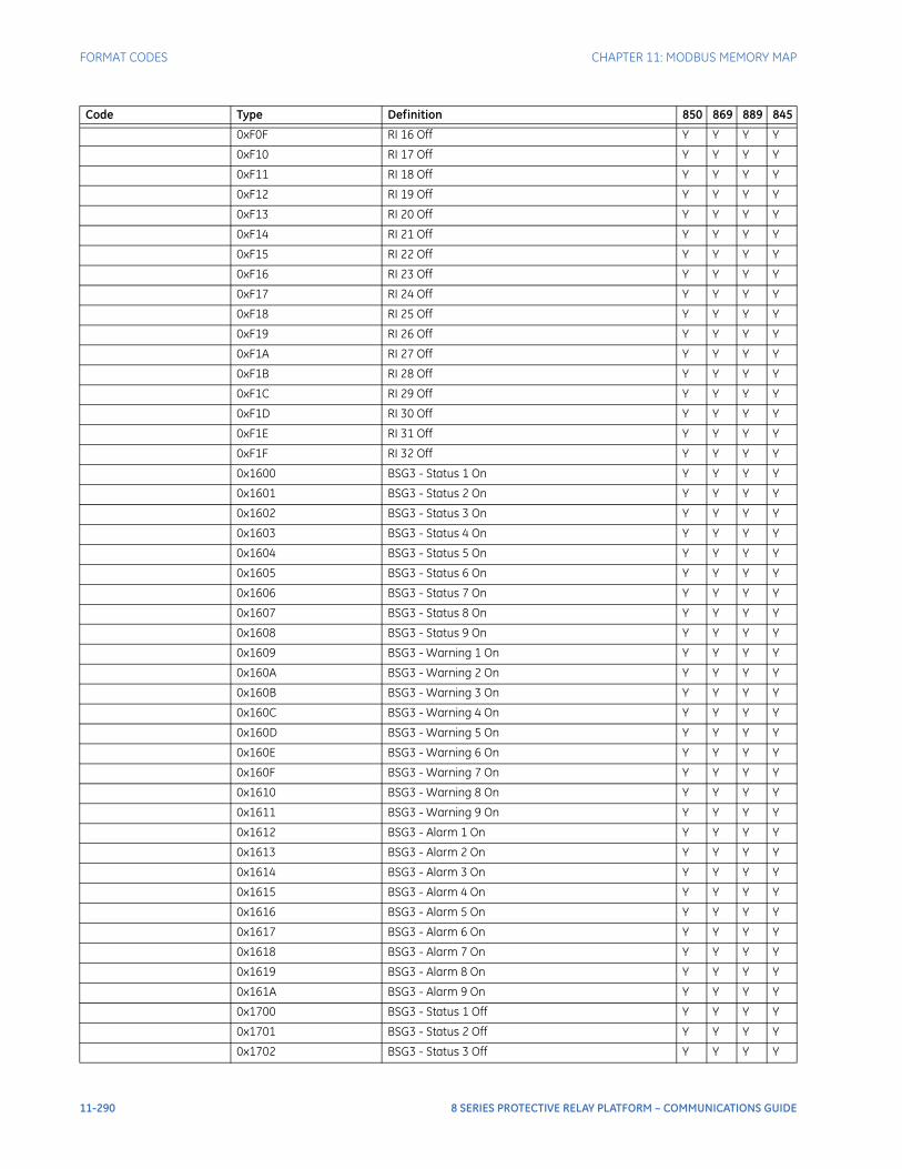
FORMAT CODES CHAPTER 11: MODBUS MEMORY MAP
0xF0F RI 16 Off Y Y Y Y
0xF10 RI 17 Off Y Y Y Y
0xF11 RI 18 Off Y Y Y Y
0xF12 RI 19 Off Y Y Y Y
0xF13 RI 20 Off Y Y Y Y
0xF14 RI 21 Off Y Y Y Y
0xF15 RI 22 Off Y Y Y Y
0xF16 RI 23 Off Y Y Y Y
0xF17 RI 24 Off Y Y Y Y
0xF18 RI 25 Off Y Y Y Y
0xF19 RI 26 Off Y Y Y Y
0xF1A RI 27 Off Y Y Y Y
0xF1B RI 28 Off Y Y Y Y
0xF1C RI 29 Off Y Y Y Y
0xF1D RI 30 Off Y Y Y Y
0xF1E RI 31 Off Y Y Y Y
0xF1F RI 32 Off Y Y Y Y
0x1600 BSG3 - Status 1 On Y Y Y Y
0x1601 BSG3 - Status 2 On Y Y Y Y
0x1602 BSG3 - Status 3 On Y Y Y Y
0x1603 BSG3 - Status 4 On Y Y Y Y
0x1604 BSG3 - Status 5 On Y Y Y Y
0x1605 BSG3 - Status 6 On Y Y Y Y
0x1606 BSG3 - Status 7 On Y Y Y Y
0x1607 BSG3 - Status 8 On Y Y Y Y
0x1608 BSG3 - Status 9 On Y Y Y Y
0x1609 BSG3 - Warning 1 On Y Y Y Y
0x160A BSG3 - Warning 2 On Y Y Y Y
0x160B BSG3 - Warning 3 On Y Y Y Y
0x160C BSG3 - Warning 4 On Y Y Y Y
0x160D BSG3 - Warning 5 On Y Y Y Y
0x160E BSG3 - Warning 6 On Y Y Y Y
0x160F BSG3 - Warning 7 On Y Y Y Y
0x1610 BSG3 - Warning 8 On Y Y Y Y
0x1611 BSG3 - Warning 9 On Y Y Y Y
0x1612 BSG3 - Alarm 1 On Y Y Y Y
0x1613 BSG3 - Alarm 2 On Y Y Y Y
0x1614 BSG3 - Alarm 3 On Y Y Y Y
0x1615 BSG3 - Alarm 4 On Y Y Y Y
0x1616 BSG3 - Alarm 5 On Y Y Y Y
0x1617 BSG3 - Alarm 6 On Y Y Y Y
0x1618 BSG3 - Alarm 7 On Y Y Y Y
0x1619 BSG3 - Alarm 8 On Y Y Y Y
0x161A BSG3 - Alarm 9 On Y Y Y Y
0x1700 BSG3 - Status 1 Off Y Y Y Y
0x1701 BSG3 - Status 2 Off Y Y Y Y
0x1702 BSG3 - Status 3 Off Y Y Y Y
Code Type Definition 850 869 889 845
11-290 8 SERIES PROTECTIVE RELAY PLATFORM – COMMUNICATIONS GUIDE
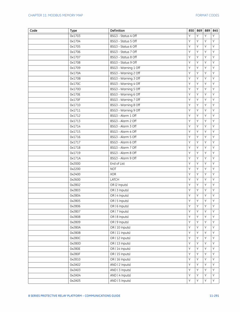
CHAPTER 11: MODBUS MEMORY MAP FORMAT CODES
0x1703 BSG3 - Status 4 Off Y Y Y Y
0x1704 BSG3 - Status 5 Off Y Y Y Y
0x1705 BSG3 - Status 6 Off Y Y Y Y
0x1706 BSG3 - Status 7 Off Y Y Y Y
0x1707 BSG3 - Status 8 Off Y Y Y Y
0x1708 BSG3 - Status 9 Off Y Y Y Y
0x1709 BSG3 - Warning 1 Off Y Y Y Y
0x170A BSG3 - Warning 2 Off Y Y Y Y
0x170B BSG3 - Warning 3 Off Y Y Y Y
0x170C BSG3 - Warning 4 Off Y Y Y Y
0x170D BSG3 - Warning 5 Off Y Y Y Y
0x170E BSG3 - Warning 6 Off Y Y Y Y
0x170F BSG3 - Warning 7 Off Y Y Y Y
0x1710 BSG3 - Warning 8 Off Y Y Y Y
0x1711 BSG3 - Warning 9 Off Y Y Y Y
0x1712 BSG3 - Alarm 1 Off Y Y Y Y
0x1713 BSG3 - Alarm 2 Off Y Y Y Y
0x1714 BSG3 - Alarm 3 Off Y Y Y Y
0x1715 BSG3 - Alarm 4 Off Y Y Y Y
0x1716 BSG3 - Alarm 5 Off Y Y Y Y
0x1717 BSG3 - Alarm 6 Off Y Y Y Y
0x1718 BSG3 - Alarm 7 Off Y Y Y Y
0x1719 BSG3 - Alarm 8 Off Y Y Y Y
0x171A BSG3 - Alarm 9 Off Y Y Y Y
0x2000 End of List Y Y Y Y
0x2200 NOT Y Y Y Y
0x2400 XOR Y Y Y Y
0x2600 LATCH Y Y Y Y
0x2802 OR (2 Inputs) Y Y Y Y
0x2803 OR ( 3 Inputs) Y Y Y Y
0x2804 OR ( 4 Inputs) Y Y Y Y
0x2805 OR ( 5 Inputs) Y Y Y Y
0x2806 OR ( 6 Inputs) Y Y Y Y
0x2807 OR ( 7 Inputs) Y Y Y Y
0x2808 OR ( 8 Inputs) Y Y Y Y
0x2809 OR ( 9 Inputs) Y Y Y Y
0x280A OR ( 10 Inputs) Y Y Y Y
0x280B OR ( 11 Inputs) Y Y Y Y
0x280C OR ( 12 Inputs) Y Y Y Y
0x280D OR ( 13 Inputs) Y Y Y Y
0x280E OR ( 14 Inputs) Y Y Y Y
0x280F OR ( 15 Inputs) Y Y Y Y
0x2810 OR ( 16 Inputs) Y Y Y Y
0x2A02 AND ( 2 Inputs) Y Y Y Y
0x2A03 AND ( 3 Inputs) Y Y Y Y
0x2A04 AND ( 4 Inputs) Y Y Y Y
0x2A05 AND ( 5 Inputs) Y Y Y Y
Code Type Definition 850 869 889 845
8 SERIES PROTECTIVE RELAY PLATFORM – COMMUNICATIONS GUIDE 11-291
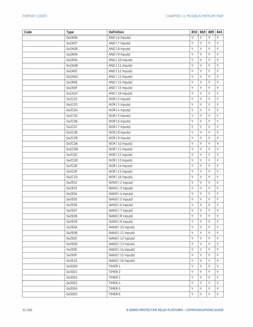
FORMAT CODES CHAPTER 11: MODBUS MEMORY MAP
0x2A06 AND ( 6 Inputs) Y Y Y Y
0x2A07 AND ( 7 Inputs) Y Y Y Y
0x2A08 AND ( 8 Inputs) Y Y Y Y
0x2A09 AND ( 9 Inputs) Y Y Y Y
0x2A0A AND ( 10 Inputs) Y Y Y Y
0x2A0B AND ( 11 Inputs) Y Y Y Y
0x2A0C AND ( 12 Inputs) Y Y Y Y
0x2A0D AND ( 13 Inputs) Y Y Y Y
0x2A0E AND ( 14 Inputs) Y Y Y Y
0x2A0F AND ( 15 Inputs) Y Y Y Y
0x2A10 AND ( 16 Inputs) Y Y Y Y
0x2C02 NOR ( 2 Inputs) Y Y Y Y
0x2C03 NOR ( 3 Inputs) Y Y Y Y
0x2C04 NOR ( 4 Inputs) Y Y Y Y
0x2C05 NOR ( 5 Inputs) Y Y Y Y
0x2C06 NOR ( 6 Inputs) Y Y Y Y
0x2C07 NOR ( 7 Inputs) Y Y Y Y
0x2C08 NOR ( 8 Inputs) Y Y Y Y
0x2C09 NOR ( 9 Inputs) Y Y Y Y
0x2C0A NOR ( 10 Inputs) Y Y Y Y
0x2C0B NOR ( 11 Inputs) Y Y Y Y
0x2C0C NOR ( 12 Inputs) Y Y Y Y
0x2C0D NOR ( 13 Inputs) Y Y Y Y
0x2C0E NOR ( 14 Inputs) Y Y Y Y
0x2C0F NOR ( 15 Inputs) Y Y Y Y
0x2C10 NOR ( 16 Inputs) Y Y Y Y
0x2E02 NAND ( 2 Inputs) Y Y Y Y
0x2E03 NAND ( 3 Inputs) Y Y Y Y
0x2E04 NAND ( 4 Inputs) Y Y Y Y
0x2E05 NAND ( 5 Inputs) Y Y Y Y
0x2E06 NAND ( 6 Inputs) Y Y Y Y
0x2E07 NAND ( 7 Inputs) Y Y Y Y
0x2E08 NAND ( 8 Inputs) Y Y Y Y
0x2E09 NAND ( 9 Inputs) Y Y Y Y
0x2E0A NAND ( 10 Inputs) Y Y Y Y
0x2E0B NAND ( 11 Inputs) Y Y Y Y
0x2E0C NAND ( 12 Inputs) Y Y Y Y
0x2E0D NAND ( 13 Inputs) Y Y Y Y
0x2E0E NAND ( 14 Inputs) Y Y Y Y
0x2E0F NAND ( 15 Inputs) Y Y Y Y
0x2E10 NAND ( 16 Inputs) Y Y Y Y
0x3000 TIMER 1 Y Y Y Y
0x3001 TIMER 2 Y Y Y Y
0x3002 TIMER 3 Y Y Y Y
0x3003 TIMER 4 Y Y Y Y
0x3004 TIMER 5 Y Y Y Y
0x3005 TIMER 6 Y Y Y Y
Code Type Definition 850 869 889 845
11-292 8 SERIES PROTECTIVE RELAY PLATFORM – COMMUNICATIONS GUIDE
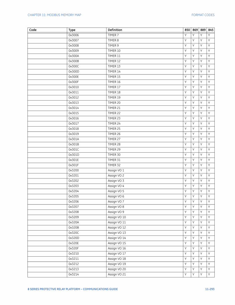
CHAPTER 11: MODBUS MEMORY MAP FORMAT CODES
0x3006 TIMER 7 Y Y Y Y
0x3007 TIMER 8 Y Y Y Y
0x3008 TIMER 9 Y Y Y Y
0x3009 TIMER 10 Y Y Y Y
0x300A TIMER 11 Y Y Y Y
0x300B TIMER 12 Y Y Y Y
0x300C TIMER 13 Y Y Y Y
0x300D TIMER 14 Y Y Y Y
0x300E TIMER 15 Y Y Y Y
0x300F TIMER 16 Y Y Y Y
0x3010 TIMER 17 Y Y Y Y
0x3011 TIMER 18 Y Y Y Y
0x3012 TIMER 19 Y Y Y Y
0x3013 TIMER 20 Y Y Y Y
0x3014 TIMER 21 Y Y Y Y
0x3015 TIMER 22 Y Y Y Y
0x3016 TIMER 23 Y Y Y Y
0x3017 TIMER 24 Y Y Y Y
0x3018 TIMER 25 Y Y Y Y
0x3019 TIMER 26 Y Y Y Y
0x301A TIMER 27 Y Y Y Y
0x301B TIMER 28 Y Y Y Y
0x301C TIMER 29 Y Y Y Y
0x301D TIMER 30 Y Y Y Y
0x301E TIMER 31 Y Y Y Y
0x301F TIMER 32 Y Y Y Y
0x3200 Assign VO 1 Y Y Y Y
0x3201 Assign VO 2 Y Y Y Y
0x3202 Assign VO 3 Y Y Y Y
0x3203 Assign VO 4 Y Y Y Y
0x3204 Assign VO 5 Y Y Y Y
0x3205 Assign VO 6 Y Y Y Y
0x3206 Assign VO 7 Y Y Y Y
0x3207 Assign VO 8 Y Y Y Y
0x3208 Assign VO 9 Y Y Y Y
0x3209 Assign VO 10 Y Y Y Y
0x320A Assign VO 11 Y Y Y Y
0x320B Assign VO 12 Y Y Y Y
0x320C Assign VO 13 Y Y Y Y
0x320D Assign VO 14 Y Y Y Y
0x320E Assign VO 15 Y Y Y Y
0x320F Assign VO 16 Y Y Y Y
0x3210 Assign VO 17 Y Y Y Y
0x3211 Assign VO 18 Y Y Y Y
0x3212 Assign VO 19 Y Y Y Y
0x3213 Assign VO 20 Y Y Y Y
0x3214 Assign VO 21 Y Y Y Y
Code Type Definition 850 869 889 845
8 SERIES PROTECTIVE RELAY PLATFORM – COMMUNICATIONS GUIDE 11-293
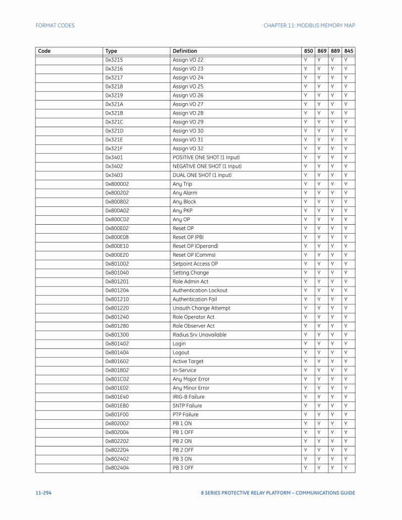
FORMAT CODES CHAPTER 11: MODBUS MEMORY MAP
0x3215 Assign VO 22 Y Y Y Y
0x3216 Assign VO 23 Y Y Y Y
0x3217 Assign VO 24 Y Y Y Y
0x3218 Assign VO 25 Y Y Y Y
0x3219 Assign VO 26 Y Y Y Y
0x321A Assign VO 27 Y Y Y Y
0x321B Assign VO 28 Y Y Y Y
0x321C Assign VO 29 Y Y Y Y
0x321D Assign VO 30 Y Y Y Y
0x321E Assign VO 31 Y Y Y Y
0x321F Assign VO 32 Y Y Y Y
0x3401 POSITIVE ONE SHOT (1 Input) Y Y Y Y
0x3402 NEGATIVE ONE SHOT (1 Input) Y Y Y Y
0x3403 DUAL ONE SHOT (1 Input) Y Y Y Y
0x800002 Any Trip Y Y Y Y
0x800202 Any Alarm Y Y Y Y
0x800802 Any Block Y Y Y Y
0x800A02 Any PKP Y Y Y Y
0x800C02 Any OP Y Y Y Y
0x800E02 Reset OP Y Y Y Y
0x800E08 Reset OP (PB) Y Y Y Y
0x800E10 Reset OP (Operand) Y Y Y Y
0x800E20 Reset OP (Comms) Y Y Y Y
0x801002 Setpoint Access OP Y Y Y Y
0x801040 Setting Change Y Y Y Y
0x801201 Role Admin Act Y Y Y Y
0x801204 Authentication Lockout Y Y Y Y
0x801210 Authentication Fail Y Y Y Y
0x801220 Unauth Change Attempt Y Y Y Y
0x801240 Role Operator Act Y Y Y Y
0x801280 Role Observer Act Y Y Y Y
0x801300 Radius Srv Unavailable Y Y Y Y
0x801402 Login Y Y Y Y
0x801404 Logout Y Y Y Y
0x801602 Active Target Y Y Y Y
0x801802 In-Service Y Y Y Y
0x801C02 Any Major Error Y Y Y Y
0x801E02 Any Minor Error Y Y Y Y
0x801E40 IRIG-B Failure Y Y Y Y
0x801E80 SNTP Failure Y Y Y Y
0x801F00 PTP Failure Y Y Y Y
0x802002 PB 1 ON Y Y Y Y
0x802004 PB 1 OFF Y Y Y Y
0x802202 PB 2 ON Y Y Y Y
0x802204 PB 2 OFF Y Y Y Y
0x802402 PB 3 ON Y Y Y Y
0x802404 PB 3 OFF Y Y Y Y
Code Type Definition 850 869 889 845
11-294 8 SERIES PROTECTIVE RELAY PLATFORM – COMMUNICATIONS GUIDE
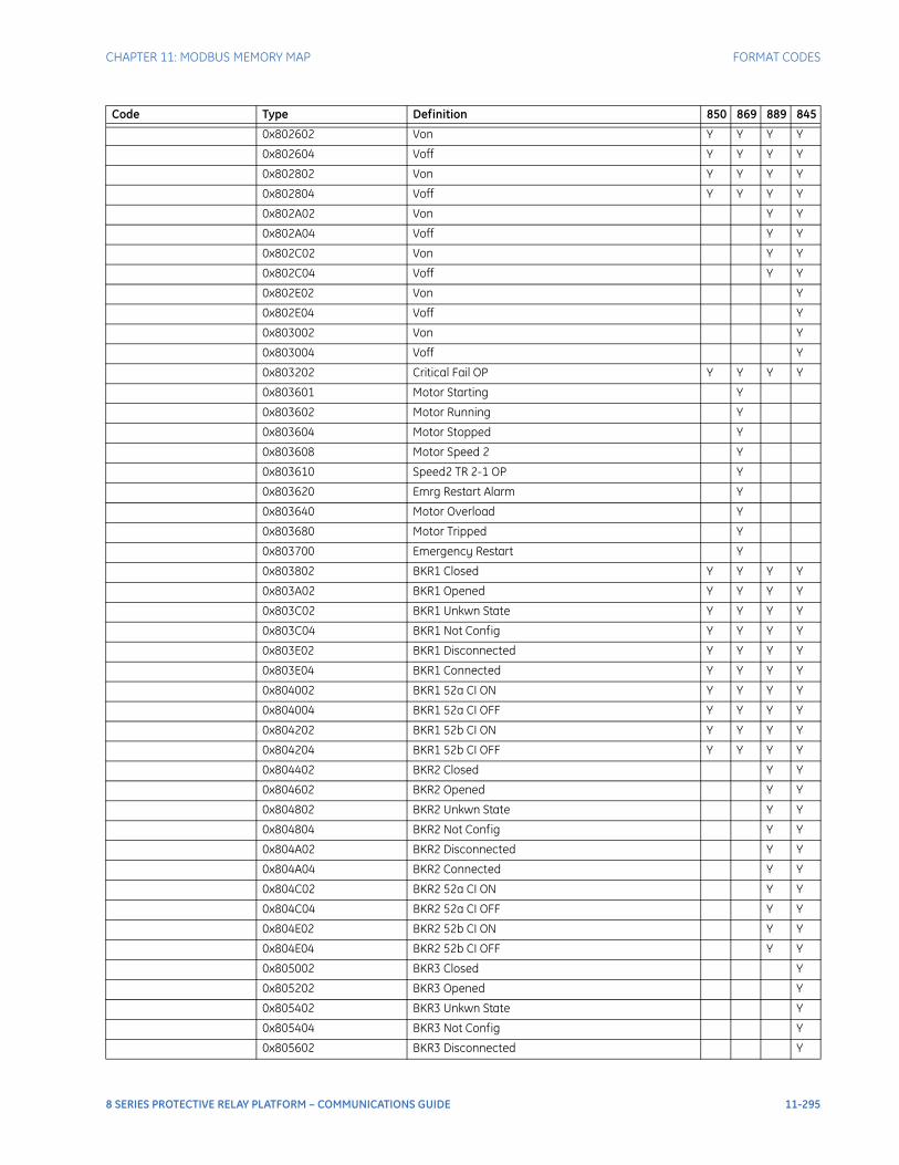
CHAPTER 11: MODBUS MEMORY MAP FORMAT CODES
0x802602 Von Y Y Y Y
0x802604 Voff Y Y Y Y
0x802802 Von Y Y Y Y
0x802804 Voff Y Y Y Y
0x802A02 Von Y Y
0x802A04 Voff Y Y
0x802C02 Von Y Y
0x802C04 Voff Y Y
0x802E02 Von Y
0x802E04 Voff Y
0x803002 Von Y
0x803004 Voff Y
0x803202 Critical Fail OP Y Y Y Y
0x803601 Motor Starting Y
0x803602 Motor Running Y
0x803604 Motor Stopped Y
0x803608 Motor Speed 2 Y
0x803610 Speed2 TR 2-1 OP Y
0x803620 Emrg Restart Alarm Y
0x803640 Motor Overload Y
0x803680 Motor Tripped Y
0x803700 Emergency Restart Y
0x803802 BKR1 Closed Y Y Y Y
0x803A02 BKR1 Opened Y Y Y Y
0x803C02 BKR1 Unkwn State Y Y Y Y
0x803C04 BKR1 Not Config Y Y Y Y
0x803E02 BKR1 Disconnected Y Y Y Y
0x803E04 BKR1 Connected Y Y Y Y
0x804002 BKR1 52a CI ON Y Y Y Y
0x804004 BKR1 52a CI OFF Y Y Y Y
0x804202 BKR1 52b CI ON Y Y Y Y
0x804204 BKR1 52b CI OFF Y Y Y Y
0x804402 BKR2 Closed Y Y
0x804602 BKR2 Opened Y Y
0x804802 BKR2 Unkwn State Y Y
0x804804 BKR2 Not Config Y Y
0x804A02 BKR2 Disconnected Y Y
0x804A04 BKR2 Connected Y Y
0x804C02 BKR2 52a CI ON Y Y
0x804C04 BKR2 52a CI OFF Y Y
0x804E02 BKR2 52b CI ON Y Y
0x804E04 BKR2 52b CI OFF Y Y
0x805002 BKR3 Closed Y
0x805202 BKR3 Opened Y
0x805402 BKR3 Unkwn State Y
0x805404 BKR3 Not Config Y
0x805602 BKR3 Disconnected Y
Code Type Definition 850 869 889 845
8 SERIES PROTECTIVE RELAY PLATFORM – COMMUNICATIONS GUIDE 11-295
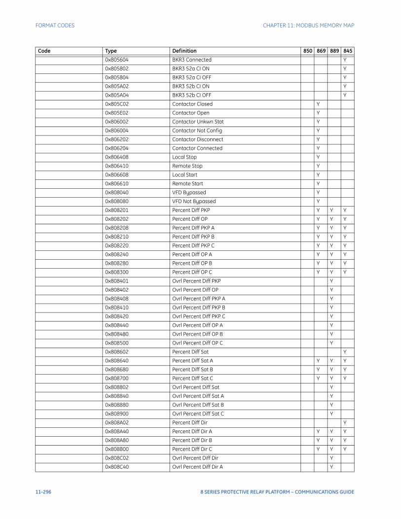
FORMAT CODES CHAPTER 11: MODBUS MEMORY MAP
0x805604 BKR3 Connected Y
0x805802 BKR3 52a CI ON Y
0x805804 BKR3 52a CI OFF Y
0x805A02 BKR3 52b CI ON Y
0x805A04 BKR3 52b CI OFF Y
0x805C02 Contactor Closed Y
0x805E02 Contactor Open Y
0x806002 Contactor Unkwn Stat Y
0x806004 Contactor Not Config Y
0x806202 Contactor Disconnect Y
0x806204 Contactor Connected Y
0x806408 Local Stop Y
0x806410 Remote Stop Y
0x806608 Local Start Y
0x806610 Remote Start Y
0x808040 VFD Bypassed Y
0x808080 VFD Not Bypassed Y
0x808201 Percent Diff PKP Y Y Y
0x808202 Percent Diff OP Y Y Y
0x808208 Percent Diff PKP A Y Y Y
0x808210 Percent Diff PKP B Y Y Y
0x808220 Percent Diff PKP C Y Y Y
0x808240 Percent Diff OP A Y Y Y
0x808280 Percent Diff OP B Y Y Y
0x808300 Percent Diff OP C Y Y Y
0x808401 Ovrl Percent Diff PKP Y
0x808402 Ovrl Percent Diff OP Y
0x808408 Ovrl Percent Diff PKP A Y
0x808410 Ovrl Percent Diff PKP B Y
0x808420 Ovrl Percent Diff PKP C Y
0x808440 Ovrl Percent Diff OP A Y
0x808480 Ovrl Percent Diff OP B Y
0x808500 Ovrl Percent Diff OP C Y
0x808602 Percent Diff Sat Y
0x808640 Percent Diff Sat A Y Y Y
0x808680 Percent Diff Sat B Y Y Y
0x808700 Percent Diff Sat C Y Y Y
0x808802 Ovrl Percent Diff Sat Y
0x808840 Ovrl Percent Diff Sat A Y
0x808880 Ovrl Percent Diff Sat B Y
0x808900 Ovrl Percent Diff Sat C Y
0x808A02 Percent Diff Dir Y
0x808A40 Percent Diff Dir A Y Y Y
0x808A80 Percent Diff Dir B Y Y Y
0x808B00 Percent Diff Dir C Y Y Y
0x808C02 Ovrl Percent Diff Dir Y
0x808C40 Ovrl Percent Diff Dir A Y
Code Type Definition 850 869 889 845
11-296 8 SERIES PROTECTIVE RELAY PLATFORM – COMMUNICATIONS GUIDE
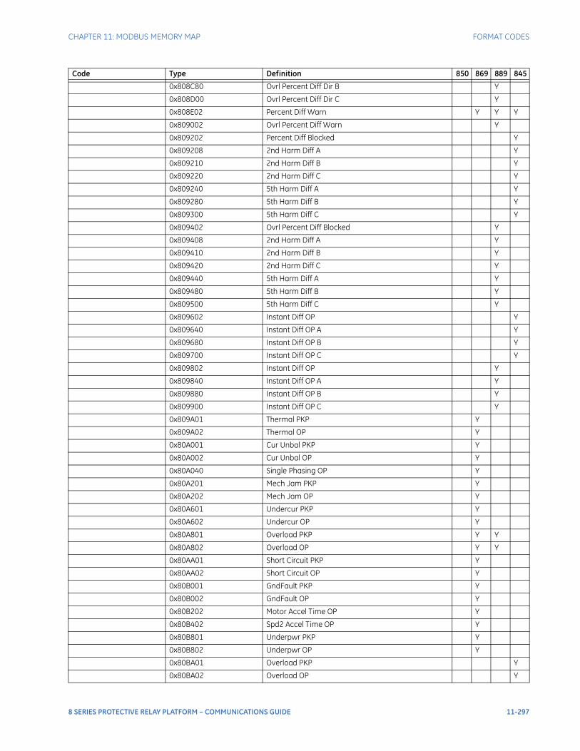
CHAPTER 11: MODBUS MEMORY MAP FORMAT CODES
0x808C80 Ovrl Percent Diff Dir B Y
0x808D00 Ovrl Percent Diff Dir C Y
0x808E02 Percent Diff Warn Y Y Y
0x809002 Ovrl Percent Diff Warn Y
0x809202 Percent Diff Blocked Y
0x809208 2nd Harm Diff A Y
0x809210 2nd Harm Diff B Y
0x809220 2nd Harm Diff C Y
0x809240 5th Harm Diff A Y
0x809280 5th Harm Diff B Y
0x809300 5th Harm Diff C Y
0x809402 Ovrl Percent Diff Blocked Y
0x809408 2nd Harm Diff A Y
0x809410 2nd Harm Diff B Y
0x809420 2nd Harm Diff C Y
0x809440 5th Harm Diff A Y
0x809480 5th Harm Diff B Y
0x809500 5th Harm Diff C Y
0x809602 Instant Diff OP Y
0x809640 Instant Diff OP A Y
0x809680 Instant Diff OP B Y
0x809700 Instant Diff OP C Y
0x809802 Instant Diff OP Y
0x809840 Instant Diff OP A Y
0x809880 Instant Diff OP B Y
0x809900 Instant Diff OP C Y
0x809A01 Thermal PKP Y
0x809A02 Thermal OP Y
0x80A001 Cur Unbal PKP Y
0x80A002 Cur Unbal OP Y
0x80A040 Single Phasing OP Y
0x80A201 Mech Jam PKP Y
0x80A202 Mech Jam OP Y
0x80A601 Undercur PKP Y
0x80A602 Undercur OP Y
0x80A801 Overload PKP Y Y
0x80A802 Overload OP Y Y
0x80AA01 Short Circuit PKP Y
0x80AA02 Short Circuit OP Y
0x80B001 GndFault PKP Y
0x80B002 GndFault OP Y
0x80B202 Motor Accel Time OP Y
0x80B402 Spd2 Accel Time OP Y
0x80B801 Underpwr PKP Y
0x80B802 Underpwr OP Y
0x80BA01 Overload PKP Y
0x80BA02 Overload OP Y
Code Type Definition 850 869 889 845
8 SERIES PROTECTIVE RELAY PLATFORM – COMMUNICATIONS GUIDE 11-297
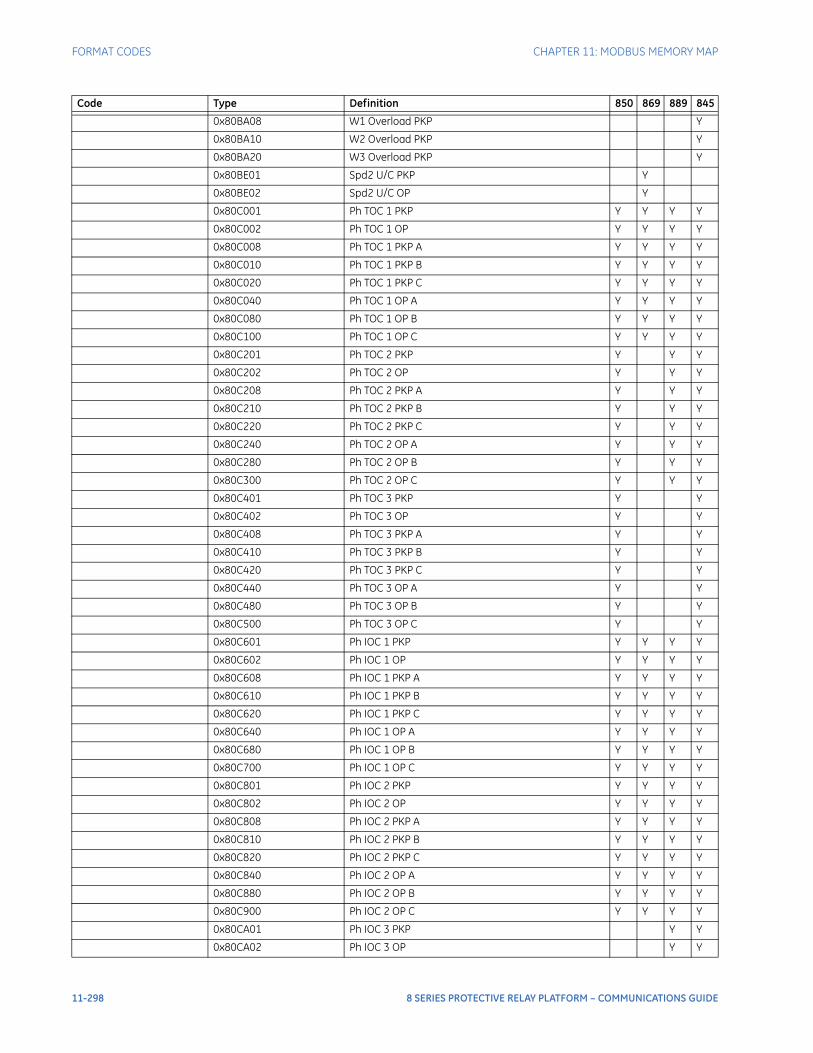
FORMAT CODES CHAPTER 11: MODBUS MEMORY MAP
0x80BA08 W1 Overload PKP Y
0x80BA10 W2 Overload PKP Y
0x80BA20 W3 Overload PKP Y
0x80BE01 Spd2 U/C PKP Y
0x80BE02 Spd2 U/C OP Y
0x80C001 Ph TOC 1 PKP Y Y Y Y
0x80C002 Ph TOC 1 OP Y Y Y Y
0x80C008 Ph TOC 1 PKP A Y Y Y Y
0x80C010 Ph TOC 1 PKP B Y Y Y Y
0x80C020 Ph TOC 1 PKP C Y Y Y Y
0x80C040 Ph TOC 1 OP A Y Y Y Y
0x80C080 Ph TOC 1 OP B Y Y Y Y
0x80C100 Ph TOC 1 OP C Y Y Y Y
0x80C201 Ph TOC 2 PKP Y Y Y
0x80C202 Ph TOC 2 OP Y Y Y
0x80C208 Ph TOC 2 PKP A Y Y Y
0x80C210 Ph TOC 2 PKP B Y Y Y
0x80C220 Ph TOC 2 PKP C Y Y Y
0x80C240 Ph TOC 2 OP A Y Y Y
0x80C280 Ph TOC 2 OP B Y Y Y
0x80C300 Ph TOC 2 OP C Y Y Y
0x80C401 Ph TOC 3 PKP Y Y
0x80C402 Ph TOC 3 OP Y Y
0x80C408 Ph TOC 3 PKP A Y Y
0x80C410 Ph TOC 3 PKP B Y Y
0x80C420 Ph TOC 3 PKP C Y Y
0x80C440 Ph TOC 3 OP A Y Y
0x80C480 Ph TOC 3 OP B Y Y
0x80C500 Ph TOC 3 OP C Y Y
0x80C601 Ph IOC 1 PKP Y Y Y Y
0x80C602 Ph IOC 1 OP Y Y Y Y
0x80C608 Ph IOC 1 PKP A Y Y Y Y
0x80C610 Ph IOC 1 PKP B Y Y Y Y
0x80C620 Ph IOC 1 PKP C Y Y Y Y
0x80C640 Ph IOC 1 OP A Y Y Y Y
0x80C680 Ph IOC 1 OP B Y Y Y Y
0x80C700 Ph IOC 1 OP C Y Y Y Y
0x80C801 Ph IOC 2 PKP Y Y Y Y
0x80C802 Ph IOC 2 OP Y Y Y Y
0x80C808 Ph IOC 2 PKP A Y Y Y Y
0x80C810 Ph IOC 2 PKP B Y Y Y Y
0x80C820 Ph IOC 2 PKP C Y Y Y Y
0x80C840 Ph IOC 2 OP A Y Y Y Y
0x80C880 Ph IOC 2 OP B Y Y Y Y
0x80C900 Ph IOC 2 OP C Y Y Y Y
0x80CA01 Ph IOC 3 PKP Y Y
0x80CA02 Ph IOC 3 OP Y Y
Code Type Definition 850 869 889 845
11-298 8 SERIES PROTECTIVE RELAY PLATFORM – COMMUNICATIONS GUIDE
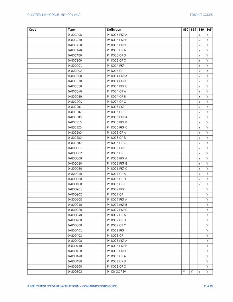
CHAPTER 11: MODBUS MEMORY MAP FORMAT CODES
0x80CA08 Ph IOC 3 PKP A Y Y
0x80CA10 Ph IOC 3 PKP B Y Y
0x80CA20 Ph IOC 3 PKP C Y Y
0x80CA40 Ph IOC 3 OP A Y Y
0x80CA80 Ph IOC 3 OP B Y Y
0x80CB00 Ph IOC 3 OP C Y Y
0x80CC01 Ph IOC 4 PKP Y Y
0x80CC02 Ph IOC 4 OP Y Y
0x80CC08 Ph IOC 4 PKP A Y Y
0x80CC10 Ph IOC 4 PKP B Y Y
0x80CC20 Ph IOC 4 PKP C Y Y
0x80CC40 Ph IOC 4 OP A Y Y
0x80CC80 Ph IOC 4 OP B Y Y
0x80CD00 Ph IOC 4 OP C Y Y
0x80CE01 Ph IOC 5 PKP Y Y
0x80CE02 Ph IOC 5 OP Y Y
0x80CE08 Ph IOC 5 PKP A Y Y
0x80CE10 Ph IOC 5 PKP B Y Y
0x80CE20 Ph IOC 5 PKP C Y Y
0x80CE40 Ph IOC 5 OP A Y Y
0x80CE80 Ph IOC 5 OP B Y Y
0x80CF00 Ph IOC 5 OP C Y Y
0x80D001 Ph IOC 6 PKP Y Y
0x80D002 Ph IOC 6 OP Y Y
0x80D008 Ph IOC 6 PKP A Y Y
0x80D010 Ph IOC 6 PKP B Y Y
0x80D020 Ph IOC 6 PKP C Y Y
0x80D040 Ph IOC 6 OP A Y Y
0x80D080 Ph IOC 6 OP B Y Y
0x80D100 Ph IOC 6 OP C Y Y
0x80D201 Ph IOC 7 PKP Y
0x80D202 Ph IOC 7 OP Y
0x80D208 Ph IOC 7 PKP A Y
0x80D210 Ph IOC 7 PKP B Y
0x80D220 Ph IOC 7 PKP C Y
0x80D240 Ph IOC 7 OP A Y
0x80D280 Ph IOC 7 OP B Y
0x80D300 Ph IOC 7 OP C Y
0x80D401 Ph IOC 8 PKP Y
0x80D402 Ph IOC 8 OP Y
0x80D408 Ph IOC 8 PKP A Y
0x80D410 Ph IOC 8 PKP B Y
0x80D420 Ph IOC 8 PKP C Y
0x80D440 Ph IOC 8 OP A Y
0x80D480 Ph IOC 8 OP B Y
0x80D500 Ph IOC 8 OP C Y
0x80D602 Ph Dir OC REV Y Y Y Y
Code Type Definition 850 869 889 845
8 SERIES PROTECTIVE RELAY PLATFORM – COMMUNICATIONS GUIDE 11-299
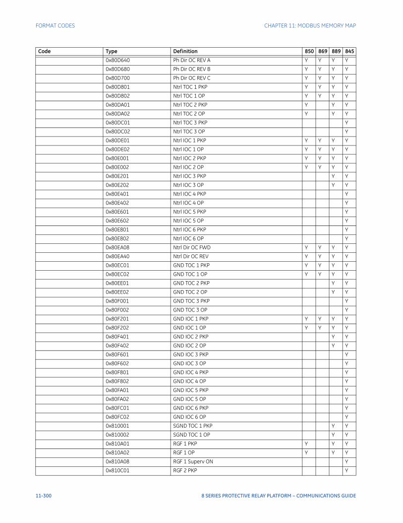
FORMAT CODES CHAPTER 11: MODBUS MEMORY MAP
0x80D640 Ph Dir OC REV A Y Y Y Y
0x80D680 Ph Dir OC REV B Y Y Y Y
0x80D700 Ph Dir OC REV C Y Y Y Y
0x80D801 Ntrl TOC 1 PKP Y Y Y Y
0x80D802 Ntrl TOC 1 OP Y Y Y Y
0x80DA01 Ntrl TOC 2 PKP Y Y Y
0x80DA02 Ntrl TOC 2 OP Y Y Y
0x80DC01 Ntrl TOC 3 PKP Y
0x80DC02 Ntrl TOC 3 OP Y
0x80DE01 Ntrl IOC 1 PKP Y Y Y Y
0x80DE02 Ntrl IOC 1 OP Y Y Y Y
0x80E001 Ntrl IOC 2 PKP Y Y Y Y
0x80E002 Ntrl IOC 2 OP Y Y Y Y
0x80E201 Ntrl IOC 3 PKP Y Y
0x80E202 Ntrl IOC 3 OP Y Y
0x80E401 Ntrl IOC 4 PKP Y
0x80E402 Ntrl IOC 4 OP Y
0x80E601 Ntrl IOC 5 PKP Y
0x80E602 Ntrl IOC 5 OP Y
0x80E801 Ntrl IOC 6 PKP Y
0x80E802 Ntrl IOC 6 OP Y
0x80EA08 Ntrl Dir OC FWD Y Y Y Y
0x80EA40 Ntrl Dir OC REV Y Y Y Y
0x80EC01 GND TOC 1 PKP Y Y Y Y
0x80EC02 GND TOC 1 OP Y Y Y Y
0x80EE01 GND TOC 2 PKP Y Y
0x80EE02 GND TOC 2 OP Y Y
0x80F001 GND TOC 3 PKP Y
0x80F002 GND TOC 3 OP Y
0x80F201 GND IOC 1 PKP Y Y Y Y
0x80F202 GND IOC 1 OP Y Y Y Y
0x80F401 GND IOC 2 PKP Y Y
0x80F402 GND IOC 2 OP Y Y
0x80F601 GND IOC 3 PKP Y
0x80F602 GND IOC 3 OP Y
0x80F801 GND IOC 4 PKP Y
0x80F802 GND IOC 4 OP Y
0x80FA01 GND IOC 5 PKP Y
0x80FA02 GND IOC 5 OP Y
0x80FC01 GND IOC 6 PKP Y
0x80FC02 GND IOC 6 OP Y
0x810001 SGND TOC 1 PKP Y Y
0x810002 SGND TOC 1 OP Y Y
0x810A01 RGF 1 PKP Y Y Y
0x810A02 RGF 1 OP Y Y Y
0x810A08 RGF 1 Superv ON Y
0x810C01 RGF 2 PKP Y
Code Type Definition 850 869 889 845
11-300 8 SERIES PROTECTIVE RELAY PLATFORM – COMMUNICATIONS GUIDE
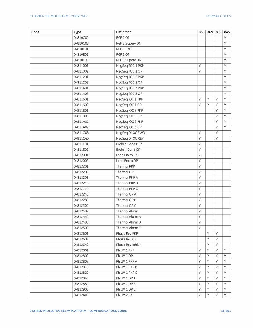
CHAPTER 11: MODBUS MEMORY MAP FORMAT CODES
0x810C02 RGF 2 OP Y
0x810C08 RGF 2 Superv ON Y
0x810E01 RGF 3 PKP Y
0x810E02 RGF 3 OP Y
0x810E08 RGF 3 Superv ON Y
0x811001 NegSeq TOC 1 PKP Y Y
0x811002 NegSeq TOC 1 OP Y Y
0x811201 NegSeq TOC 2 PKP Y
0x811202 NegSeq TOC 2 OP Y
0x811401 NegSeq TOC 3 PKP Y
0x811402 NegSeq TOC 3 OP Y
0x811601 NegSeq IOC 1 PKP Y Y Y Y
0x811602 NegSeq IOC 1 OP Y Y Y Y
0x811801 NegSeq IOC 2 PKP Y Y
0x811802 NegSeq IOC 2 OP Y Y
0x811A01 NegSeq IOC 3 PKP Y Y
0x811A02 NegSeq IOC 3 OP Y Y
0x811C08 NegSeq DirOC FWD Y Y
0x811C40 NegSeq DirOC REV Y Y
0x811E01 Broken Cond PKP Y
0x811E02 Broken Cond OP Y
0x812001 Load Encro PKP Y
0x812002 Load Encro OP Y
0x812201 Thermal PKP Y
0x812202 Thermal OP Y
0x812208 Thermal PKP A Y
0x812210 Thermal PKP B Y
0x812220 Thermal PKP C Y
0x812240 Thermal OP A Y
0x812280 Thermal OP B Y
0x812300 Thermal OP C Y
0x812402 Thermal Alarm Y
0x812440 Thermal Alarm A Y
0x812480 Thermal Alarm B Y
0x812500 Thermal Alarm C Y
0x812601 Phase Rev PKP Y Y
0x812602 Phase Rev OP Y Y
0x812640 Phase Rev Inhibit Y Y
0x812801 Ph UV 1 PKP Y Y Y Y
0x812802 Ph UV 1 OP Y Y Y Y
0x812808 Ph UV 1 PKP A Y Y Y Y
0x812810 Ph UV 1 PKP B Y Y Y Y
0x812820 Ph UV 1 PKP C Y Y Y Y
0x812840 Ph UV 1 OP A Y Y Y Y
0x812880 Ph UV 1 OP B Y Y Y Y
0x812900 Ph UV 1 OP C Y Y Y Y
0x812A01 Ph UV 2 PKP Y Y Y Y
Code Type Definition 850 869 889 845
8 SERIES PROTECTIVE RELAY PLATFORM – COMMUNICATIONS GUIDE 11-301
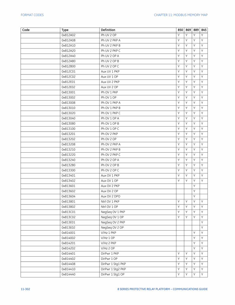
FORMAT CODES CHAPTER 11: MODBUS MEMORY MAP
0x812A02 Ph UV 2 OP Y Y Y Y
0x812A08 Ph UV 2 PKP A Y Y Y Y
0x812A10 Ph UV 2 PKP B Y Y Y Y
0x812A20 Ph UV 2 PKP C Y Y Y Y
0x812A40 Ph UV 2 OP A Y Y Y Y
0x812A80 Ph UV 2 OP B Y Y Y Y
0x812B00 Ph UV 2 OP C Y Y Y Y
0x812C01 Aux UV 1 PKP Y Y Y Y
0x812C02 Aux UV 1 OP Y Y Y Y
0x812E01 Aux UV 2 PKP Y Y Y Y
0x812E02 Aux UV 2 OP Y Y Y Y
0x813001 Ph OV 1 PKP Y Y Y Y
0x813002 Ph OV 1 OP Y Y Y Y
0x813008 Ph OV 1 PKP A Y Y Y Y
0x813010 Ph OV 1 PKP B Y Y Y Y
0x813020 Ph OV 1 PKP C Y Y Y Y
0x813040 Ph OV 1 OP A Y Y Y Y
0x813080 Ph OV 1 OP B Y Y Y Y
0x813100 Ph OV 1 OP C Y Y Y Y
0x813201 Ph OV 2 PKP Y Y Y Y
0x813202 Ph OV 2 OP Y Y Y Y
0x813208 Ph OV 2 PKP A Y Y Y Y
0x813210 Ph OV 2 PKP B Y Y Y Y
0x813220 Ph OV 2 PKP C Y Y Y Y
0x813240 Ph OV 2 OP A Y Y Y Y
0x813280 Ph OV 2 OP B Y Y Y Y
0x813300 Ph OV 2 OP C Y Y Y Y
0x813401 Aux OV 1 PKP Y Y Y Y
0x813402 Aux OV 1 OP Y Y Y Y
0x813601 Aux OV 2 PKP Y
0x813602 Aux OV 2 OP Y
0x813604 Aux OV 2 DPO Y
0x813801 Ntrl OV 1 PKP Y Y Y Y
0x813802 Ntrl OV 1 OP Y Y Y Y
0x813C01 NegSeq OV 1 PKP Y Y Y Y
0x813C02 NegSeq OV 1 OP Y Y Y Y
0x813E01 NegSeq OV 2 PKP Y
0x813E02 NegSeq OV 2 OP Y
0x814001 V/Hz 1 PKP Y Y
0x814002 V/Hz 1 OP Y Y
0x814201 V/Hz 2 PKP Y Y
0x814202 V/Hz 2 OP Y Y
0x814401 DirPwr 1 PKP Y Y Y Y
0x814402 DirPwr 1 OP Y Y Y Y
0x814408 DirPwr 1 Stg1 PKP Y Y Y Y
0x814410 DirPwr 1 Stg2 PKP Y Y Y Y
0x814440 DirPwr 1 Stg1 OP Y Y Y Y
Code Type Definition 850 869 889 845
11-302 8 SERIES PROTECTIVE RELAY PLATFORM – COMMUNICATIONS GUIDE
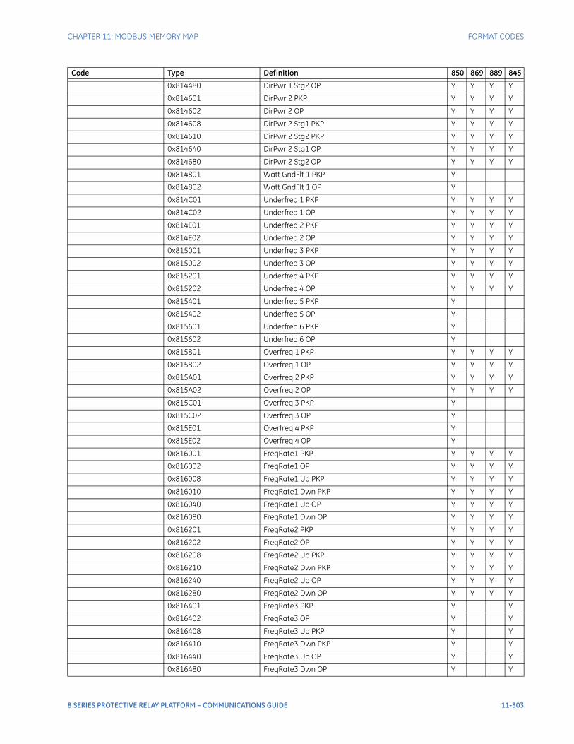
CHAPTER 11: MODBUS MEMORY MAP FORMAT CODES
0x814480 DirPwr 1 Stg2 OP Y Y Y Y
0x814601 DirPwr 2 PKP Y Y Y Y
0x814602 DirPwr 2 OP Y Y Y Y
0x814608 DirPwr 2 Stg1 PKP Y Y Y Y
0x814610 DirPwr 2 Stg2 PKP Y Y Y Y
0x814640 DirPwr 2 Stg1 OP Y Y Y Y
0x814680 DirPwr 2 Stg2 OP Y Y Y Y
0x814801 Watt GndFlt 1 PKP Y
0x814802 Watt GndFlt 1 OP Y
0x814C01 Underfreq 1 PKP Y Y Y Y
0x814C02 Underfreq 1 OP Y Y Y Y
0x814E01 Underfreq 2 PKP Y Y Y Y
0x814E02 Underfreq 2 OP Y Y Y Y
0x815001 Underfreq 3 PKP Y Y Y Y
0x815002 Underfreq 3 OP Y Y Y Y
0x815201 Underfreq 4 PKP Y Y Y Y
0x815202 Underfreq 4 OP Y Y Y Y
0x815401 Underfreq 5 PKP Y
0x815402 Underfreq 5 OP Y
0x815601 Underfreq 6 PKP Y
0x815602 Underfreq 6 OP Y
0x815801 Overfreq 1 PKP Y Y Y Y
0x815802 Overfreq 1 OP Y Y Y Y
0x815A01 Overfreq 2 PKP Y Y Y Y
0x815A02 Overfreq 2 OP Y Y Y Y
0x815C01 Overfreq 3 PKP Y
0x815C02 Overfreq 3 OP Y
0x815E01 Overfreq 4 PKP Y
0x815E02 Overfreq 4 OP Y
0x816001 FreqRate1 PKP Y Y Y Y
0x816002 FreqRate1 OP Y Y Y Y
0x816008 FreqRate1 Up PKP Y Y Y Y
0x816010 FreqRate1 Dwn PKP Y Y Y Y
0x816040 FreqRate1 Up OP Y Y Y Y
0x816080 FreqRate1 Dwn OP Y Y Y Y
0x816201 FreqRate2 PKP Y Y Y Y
0x816202 FreqRate2 OP Y Y Y Y
0x816208 FreqRate2 Up PKP Y Y Y Y
0x816210 FreqRate2 Dwn PKP Y Y Y Y
0x816240 FreqRate2 Up OP Y Y Y Y
0x816280 FreqRate2 Dwn OP Y Y Y Y
0x816401 FreqRate3 PKP Y Y
0x816402 FreqRate3 OP Y Y
0x816408 FreqRate3 Up PKP Y Y
0x816410 FreqRate3 Dwn PKP Y Y
0x816440 FreqRate3 Up OP Y Y
0x816480 FreqRate3 Dwn OP Y Y
Code Type Definition 850 869 889 845
8 SERIES PROTECTIVE RELAY PLATFORM – COMMUNICATIONS GUIDE 11-303
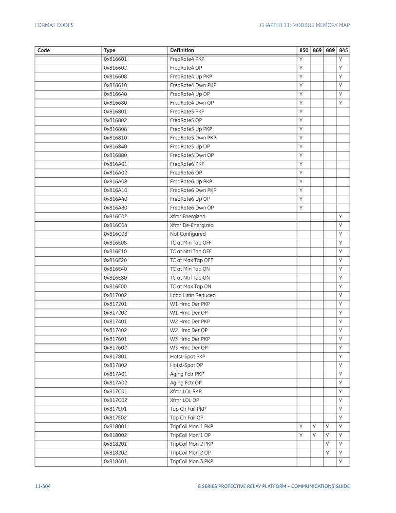
FORMAT CODES CHAPTER 11: MODBUS MEMORY MAP
0x816601 FreqRate4 PKP Y Y
0x816602 FreqRate4 OP Y Y
0x816608 FreqRate4 Up PKP Y Y
0x816610 FreqRate4 Dwn PKP Y Y
0x816640 FreqRate4 Up OP Y Y
0x816680 FreqRate4 Dwn OP Y Y
0x816801 FreqRate5 PKP Y
0x816802 FreqRate5 OP Y
0x816808 FreqRate5 Up PKP Y
0x816810 FreqRate5 Dwn PKP Y
0x816840 FreqRate5 Up OP Y
0x816880 FreqRate5 Dwn OP Y
0x816A01 FreqRate6 PKP Y
0x816A02 FreqRate6 OP Y
0x816A08 FreqRate6 Up PKP Y
0x816A10 FreqRate6 Dwn PKP Y
0x816A40 FreqRate6 Up OP Y
0x816A80 FreqRate6 Dwn OP Y
0x816C02 Xfmr Energized Y
0x816C04 Xfmr De-Energized Y
0x816C08 Not Configured Y
0x816E08 TC at Min Tap OFF Y
0x816E10 TC at Ntrl Tap OFF Y
0x816E20 TC at Max Tap OFF Y
0x816E40 TC at Min Tap ON Y
0x816E80 TC at Ntrl Tap ON Y
0x816F00 TC at Max Tap ON Y
0x817002 Load Limit Reduced Y
0x817201 W1 Hmc Der PKP Y
0x817202 W1 Hmc Der OP Y
0x817401 W2 Hmc Der PKP Y
0x817402 W2 Hmc Der OP Y
0x817601 W3 Hmc Der PKP Y
0x817602 W3 Hmc Der OP Y
0x817801 Hotst-Spot PKP Y
0x817802 Hotst-Spot OP Y
0x817A01 Aging Fctr PKP Y
0x817A02 Aging Fctr OP Y
0x817C01 Xfmr LOL PKP Y
0x817C02 Xfmr LOL OP Y
0x817E01 Tap Ch Fail PKP Y
0x817E02 Tap Ch Fail OP Y
0x818001 TripCoil Mon 1 PKP Y Y Y Y
0x818002 TripCoil Mon 1 OP Y Y Y Y
0x818201 TripCoil Mon 2 PKP Y Y
0x818202 TripCoil Mon 2 OP Y Y
0x818401 TripCoil Mon 3 PKP Y
Code Type Definition 850 869 889 845
11-304 8 SERIES PROTECTIVE RELAY PLATFORM – COMMUNICATIONS GUIDE

CHAPTER 11: MODBUS MEMORY MAP FORMAT CODES
0x818402 TripCoil Mon 3 OP Y
0x818601 Cls Coil Mon 1 PKP Y Y Y Y
0x818602 Cls Coil Mon 1 OP Y Y Y Y
0x818801 Cls Coil Mon 2 PKP Y Y
0x818802 Cls Coil Mon 2 OP Y Y
0x818A01 Cls Coil Mon 3 PKP Y
0x818A02 Cls Coil Mon 3 OP Y
0x818C02 BKR1 Arc OP Y Y Y Y
0x818E02 BKR2 Arc OP Y Y
0x819002 BKR3 Arc OP Y
0x819201 BKR1 Charge Fail Y Y Y Y
0x819202 BKR1 Hlth PKP Y Y Y Y
0x819208 BKR1 Hlth Trip PKP Y Y Y Y
0x819210 BKR1 Hlth Cls PKP Y Y Y Y
0x819220 BKR1 Hlth Chg PKP Y Y Y Y
0x819240 BKR1 Hlth OP Fail Y Y Y Y
0x819401 BKR2 Charge Fail Y
0x819402 BKR2 Hlth PKP Y
0x819408 BKR2 Hlth Trip PKP Y
0x819410 BKR2 Hlth Cls PKP Y
0x819420 BKR2 Hlth Chg PKP Y
0x819440 BKR2 Hlth OP Fail Y
0x819601 BKR3 Charge Fail Y
0x819602 BKR3 Hlth PKP Y
0x819608 BKR3 Hlth Trip PKP Y
0x819610 BKR3 Hlth Cls PKP Y
0x819620 BKR3 Hlth Chg PKP Y
0x819640 BKR3 Hlth OP Fail Y
0x819801 BKR1 Arc Fail Y Y Y Y
0x819808 BKR1 Arc PKP A Y Y Y Y
0x819810 BKR1 Arc PKP B Y Y Y Y
0x819820 BKR1 Arc PKP C Y Y Y Y
0x819840 BKR1 Engy PKP A Y Y Y Y
0x819880 BKR1 Engy PKP B Y Y Y Y
0x819900 BKR1 Engy PKP C Y Y Y Y
0x819A01 BKR2 Arc Fail Y Y
0x819A08 BKR2 Arc PKP A Y Y
0x819A10 BKR2 Arc PKP B Y Y
0x819A20 BKR2 Arc PKP C Y Y
0x819A40 BKR2 Engy PKP A Y Y
0x819A80 BKR2 Engy PKP B Y Y
0x819B00 BKR2 Engy PKP C Y Y
0x819E01 Brokn Rtr Bar PKP Y
0x819E02 Brokn Rtr Bar OP Y
0x81A008 PF 1 Switch-In Y Y Y Y
0x81A010 PF 1 Switch-Out Y Y Y Y
0x81A040 PF 1 Switch-In OP Y Y Y Y
Code Type Definition 850 869 889 845
8 SERIES PROTECTIVE RELAY PLATFORM – COMMUNICATIONS GUIDE 11-305
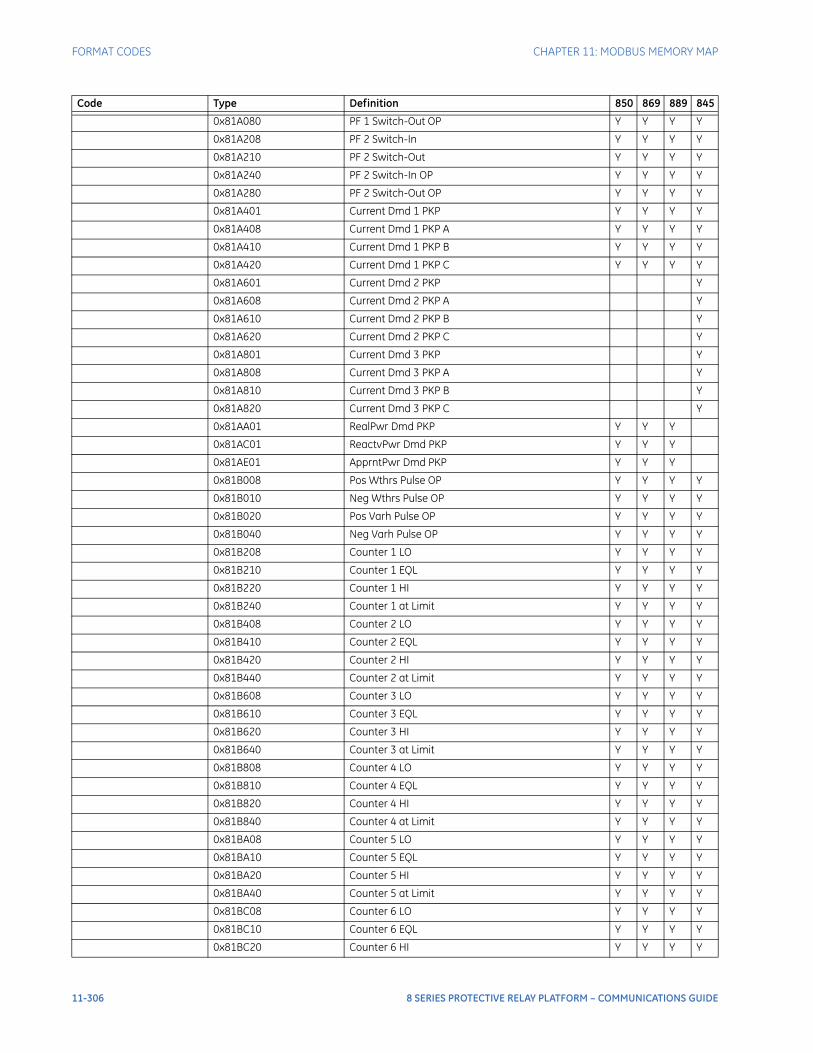
FORMAT CODES CHAPTER 11: MODBUS MEMORY MAP
0x81A080 PF 1 Switch-Out OP Y Y Y Y
0x81A208 PF 2 Switch-In Y Y Y Y
0x81A210 PF 2 Switch-Out Y Y Y Y
0x81A240 PF 2 Switch-In OP Y Y Y Y
0x81A280 PF 2 Switch-Out OP Y Y Y Y
0x81A401 Current Dmd 1 PKP Y Y Y Y
0x81A408 Current Dmd 1 PKP A Y Y Y Y
0x81A410 Current Dmd 1 PKP B Y Y Y Y
0x81A420 Current Dmd 1 PKP C Y Y Y Y
0x81A601 Current Dmd 2 PKP Y
0x81A608 Current Dmd 2 PKP A Y
0x81A610 Current Dmd 2 PKP B Y
0x81A620 Current Dmd 2 PKP C Y
0x81A801 Current Dmd 3 PKP Y
0x81A808 Current Dmd 3 PKP A Y
0x81A810 Current Dmd 3 PKP B Y
0x81A820 Current Dmd 3 PKP C Y
0x81AA01 RealPwr Dmd PKP Y Y Y
0x81AC01 ReactvPwr Dmd PKP Y Y Y
0x81AE01 ApprntPwr Dmd PKP Y Y Y
0x81B008 Pos Wthrs Pulse OP Y Y Y Y
0x81B010 Neg Wthrs Pulse OP Y Y Y Y
0x81B020 Pos Varh Pulse OP Y Y Y Y
0x81B040 Neg Varh Pulse OP Y Y Y Y
0x81B208 Counter 1 LO Y Y Y Y
0x81B210 Counter 1 EQL Y Y Y Y
0x81B220 Counter 1 HI Y Y Y Y
0x81B240 Counter 1 at Limit Y Y Y Y
0x81B408 Counter 2 LO Y Y Y Y
0x81B410 Counter 2 EQL Y Y Y Y
0x81B420 Counter 2 HI Y Y Y Y
0x81B440 Counter 2 at Limit Y Y Y Y
0x81B608 Counter 3 LO Y Y Y Y
0x81B610 Counter 3 EQL Y Y Y Y
0x81B620 Counter 3 HI Y Y Y Y
0x81B640 Counter 3 at Limit Y Y Y Y
0x81B808 Counter 4 LO Y Y Y Y
0x81B810 Counter 4 EQL Y Y Y Y
0x81B820 Counter 4 HI Y Y Y Y
0x81B840 Counter 4 at Limit Y Y Y Y
0x81BA08 Counter 5 LO Y Y Y Y
0x81BA10 Counter 5 EQL Y Y Y Y
0x81BA20 Counter 5 HI Y Y Y Y
0x81BA40 Counter 5 at Limit Y Y Y Y
0x81BC08 Counter 6 LO Y Y Y Y
0x81BC10 Counter 6 EQL Y Y Y Y
0x81BC20 Counter 6 HI Y Y Y Y
Code Type Definition 850 869 889 845
11-306 8 SERIES PROTECTIVE RELAY PLATFORM – COMMUNICATIONS GUIDE
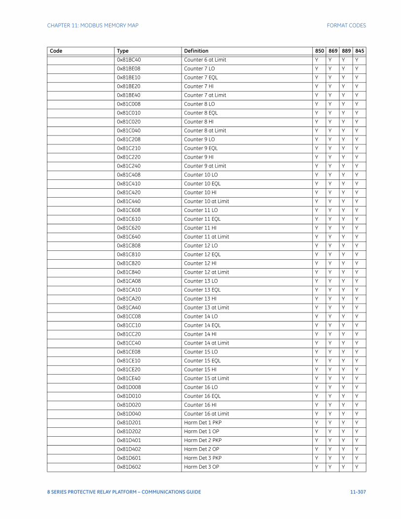
CHAPTER 11: MODBUS MEMORY MAP FORMAT CODES
0x81BC40 Counter 6 at Limit Y Y Y Y
0x81BE08 Counter 7 LO Y Y Y Y
0x81BE10 Counter 7 EQL Y Y Y Y
0x81BE20 Counter 7 HI Y Y Y Y
0x81BE40 Counter 7 at Limit Y Y Y Y
0x81C008 Counter 8 LO Y Y Y Y
0x81C010 Counter 8 EQL Y Y Y Y
0x81C020 Counter 8 HI Y Y Y Y
0x81C040 Counter 8 at Limit Y Y Y Y
0x81C208 Counter 9 LO Y Y Y Y
0x81C210 Counter 9 EQL Y Y Y Y
0x81C220 Counter 9 HI Y Y Y Y
0x81C240 Counter 9 at Limit Y Y Y Y
0x81C408 Counter 10 LO Y Y Y Y
0x81C410 Counter 10 EQL Y Y Y Y
0x81C420 Counter 10 HI Y Y Y Y
0x81C440 Counter 10 at Limit Y Y Y Y
0x81C608 Counter 11 LO Y Y Y Y
0x81C610 Counter 11 EQL Y Y Y Y
0x81C620 Counter 11 HI Y Y Y Y
0x81C640 Counter 11 at Limit Y Y Y Y
0x81C808 Counter 12 LO Y Y Y Y
0x81C810 Counter 12 EQL Y Y Y Y
0x81C820 Counter 12 HI Y Y Y Y
0x81C840 Counter 12 at Limit Y Y Y Y
0x81CA08 Counter 13 LO Y Y Y Y
0x81CA10 Counter 13 EQL Y Y Y Y
0x81CA20 Counter 13 HI Y Y Y Y
0x81CA40 Counter 13 at Limit Y Y Y Y
0x81CC08 Counter 14 LO Y Y Y Y
0x81CC10 Counter 14 EQL Y Y Y Y
0x81CC20 Counter 14 HI Y Y Y Y
0x81CC40 Counter 14 at Limit Y Y Y Y
0x81CE08 Counter 15 LO Y Y Y Y
0x81CE10 Counter 15 EQL Y Y Y Y
0x81CE20 Counter 15 HI Y Y Y Y
0x81CE40 Counter 15 at Limit Y Y Y Y
0x81D008 Counter 16 LO Y Y Y Y
0x81D010 Counter 16 EQL Y Y Y Y
0x81D020 Counter 16 HI Y Y Y Y
0x81D040 Counter 16 at Limit Y Y Y Y
0x81D201 Harm Det 1 PKP Y Y Y Y
0x81D202 Harm Det 1 OP Y Y Y Y
0x81D401 Harm Det 2 PKP Y Y Y Y
0x81D402 Harm Det 2 OP Y Y Y Y
0x81D601 Harm Det 3 PKP Y Y Y Y
0x81D602 Harm Det 3 OP Y Y Y Y
Code Type Definition 850 869 889 845
8 SERIES PROTECTIVE RELAY PLATFORM – COMMUNICATIONS GUIDE 11-307
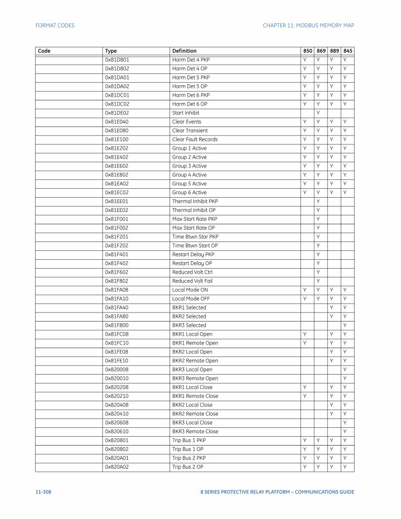
FORMAT CODES CHAPTER 11: MODBUS MEMORY MAP
0x81D801 Harm Det 4 PKP Y Y Y Y
0x81D802 Harm Det 4 OP Y Y Y Y
0x81DA01 Harm Det 5 PKP Y Y Y Y
0x81DA02 Harm Det 5 OP Y Y Y Y
0x81DC01 Harm Det 6 PKP Y Y Y Y
0x81DC02 Harm Det 6 OP Y Y Y Y
0x81DE02 Start Inhibit Y
0x81E040 Clear Events Y Y Y Y
0x81E080 Clear Transient Y Y Y Y
0x81E100 Clear Fault Records Y Y Y Y
0x81E202 Group 1 Active Y Y Y Y
0x81E402 Group 2 Active Y Y Y Y
0x81E602 Group 3 Active Y Y Y Y
0x81E802 Group 4 Active Y Y Y Y
0x81EA02 Group 5 Active Y Y Y Y
0x81EC02 Group 6 Active Y Y Y Y
0x81EE01 Thermal Inhibit PKP Y
0x81EE02 Thermal Inhibit OP Y
0x81F001 Max Start Rate PKP Y
0x81F002 Max Start Rate OP Y
0x81F201 Time Btwn Star PKP Y
0x81F202 Time Btwn Start OP Y
0x81F401 Restart Delay PKP Y
0x81F402 Restart Delay OP Y
0x81F602 Reduced Volt Ctrl Y
0x81F802 Reduced Volt Fail Y
0x81FA08 Local Mode ON Y Y Y Y
0x81FA10 Local Mode OFF Y Y Y Y
0x81FA40 BKR1 Selected Y Y
0x81FA80 BKR2 Selected Y Y
0x81FB00 BKR3 Selected Y
0x81FC08 BKR1 Local Open Y Y Y
0x81FC10 BKR1 Remote Open Y Y Y
0x81FE08 BKR2 Local Open Y Y
0x81FE10 BKR2 Remote Open Y Y
0x820008 BKR3 Local Open Y
0x820010 BKR3 Remote Open Y
0x820208 BKR1 Local Close Y Y Y
0x820210 BKR1 Remote Close Y Y Y
0x820408 BKR2 Local Close Y Y
0x820410 BKR2 Remote Close Y Y
0x820608 BKR3 Local Close Y
0x820610 BKR3 Remote Close Y
0x820801 Trip Bus 1 PKP Y Y Y Y
0x820802 Trip Bus 1 OP Y Y Y Y
0x820A01 Trip Bus 2 PKP Y Y Y Y
0x820A02 Trip Bus 2 OP Y Y Y Y
Code Type Definition 850 869 889 845
11-308 8 SERIES PROTECTIVE RELAY PLATFORM – COMMUNICATIONS GUIDE
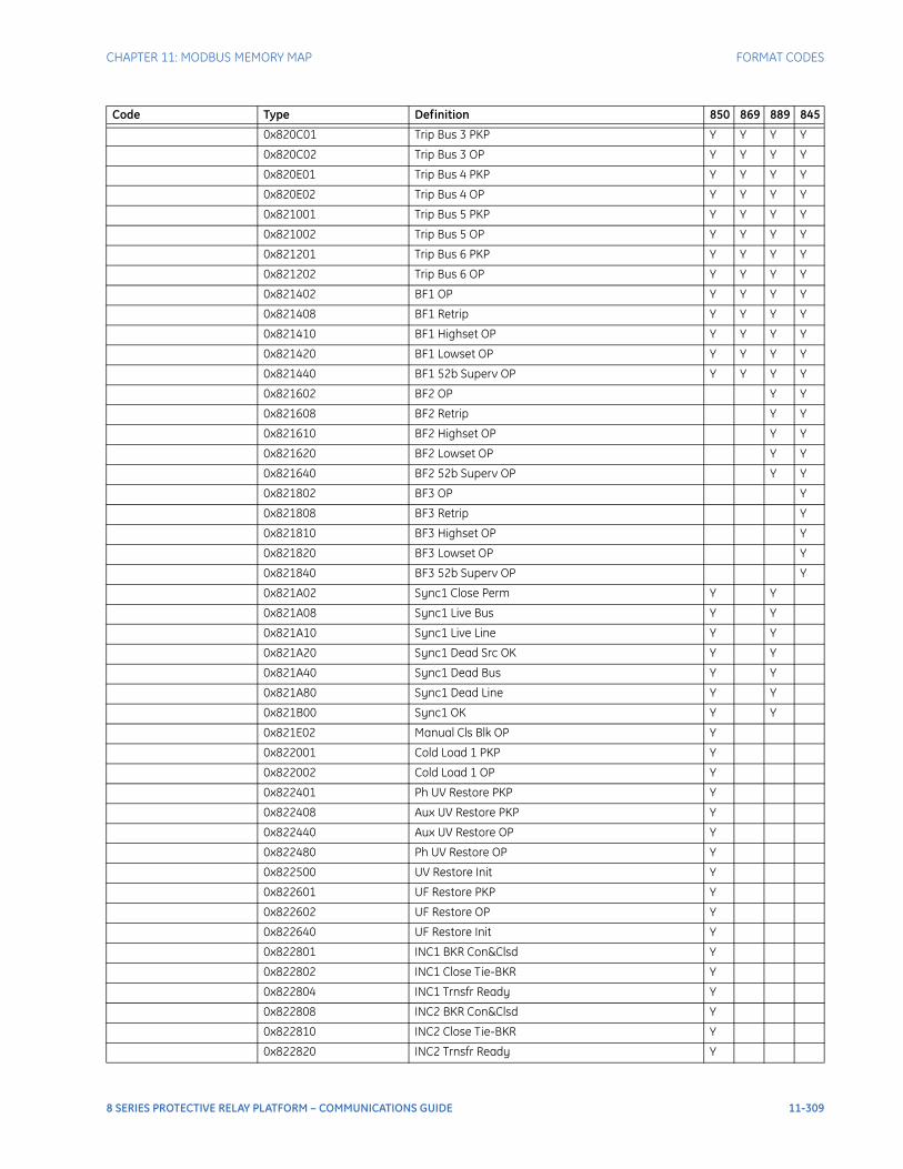
CHAPTER 11: MODBUS MEMORY MAP FORMAT CODES
0x820C01 Trip Bus 3 PKP Y Y Y Y
0x820C02 Trip Bus 3 OP Y Y Y Y
0x820E01 Trip Bus 4 PKP Y Y Y Y
0x820E02 Trip Bus 4 OP Y Y Y Y
0x821001 Trip Bus 5 PKP Y Y Y Y
0x821002 Trip Bus 5 OP Y Y Y Y
0x821201 Trip Bus 6 PKP Y Y Y Y
0x821202 Trip Bus 6 OP Y Y Y Y
0x821402 BF1 OP Y Y Y Y
0x821408 BF1 Retrip Y Y Y Y
0x821410 BF1 Highset OP Y Y Y Y
0x821420 BF1 Lowset OP Y Y Y Y
0x821440 BF1 52b Superv OP Y Y Y Y
0x821602 BF2 OP Y Y
0x821608 BF2 Retrip Y Y
0x821610 BF2 Highset OP Y Y
0x821620 BF2 Lowset OP Y Y
0x821640 BF2 52b Superv OP Y Y
0x821802 BF3 OP Y
0x821808 BF3 Retrip Y
0x821810 BF3 Highset OP Y
0x821820 BF3 Lowset OP Y
0x821840 BF3 52b Superv OP Y
0x821A02 Sync1 Close Perm Y Y
0x821A08 Sync1 Live Bus Y Y
0x821A10 Sync1 Live Line Y Y
0x821A20 Sync1 Dead Src OK Y Y
0x821A40 Sync1 Dead Bus Y Y
0x821A80 Sync1 Dead Line Y Y
0x821B00 Sync1 OK Y Y
0x821E02 Manual Cls Blk OP Y
0x822001 Cold Load 1 PKP Y
0x822002 Cold Load 1 OP Y
0x822401 Ph UV Restore PKP Y
0x822408 Aux UV Restore PKP Y
0x822440 Aux UV Restore OP Y
0x822480 Ph UV Restore OP Y
0x822500 UV Restore Init Y
0x822601 UF Restore PKP Y
0x822602 UF Restore OP Y
0x822640 UF Restore Init Y
0x822801 INC1 BKR Con&Clsd Y
0x822802 INC1 Close Tie-BKR Y
0x822804 INC1 Trnsfr Ready Y
0x822808 INC2 BKR Con&Clsd Y
0x822810 INC2 Close Tie-BKR Y
0x822820 INC2 Trnsfr Ready Y
Code Type Definition 850 869 889 845
8 SERIES PROTECTIVE RELAY PLATFORM – COMMUNICATIONS GUIDE 11-309
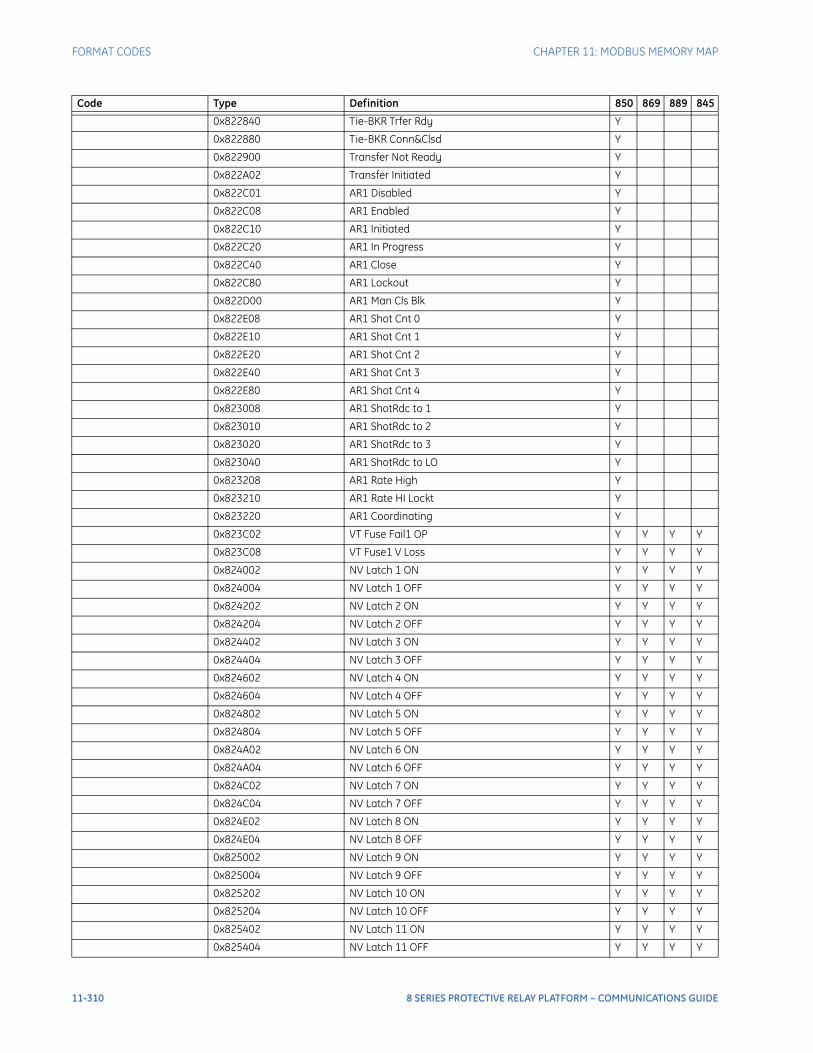
FORMAT CODES CHAPTER 11: MODBUS MEMORY MAP
0x822840 Tie-BKR Trfer Rdy Y
0x822880 Tie-BKR Conn&Clsd Y
0x822900 Transfer Not Ready Y
0x822A02 Transfer Initiated Y
0x822C01 AR1 Disabled Y
0x822C08 AR1 Enabled Y
0x822C10 AR1 Initiated Y
0x822C20 AR1 In Progress Y
0x822C40 AR1 Close Y
0x822C80 AR1 Lockout Y
0x822D00 AR1 Man Cls Blk Y
0x822E08 AR1 Shot Cnt 0 Y
0x822E10 AR1 Shot Cnt 1 Y
0x822E20 AR1 Shot Cnt 2 Y
0x822E40 AR1 Shot Cnt 3 Y
0x822E80 AR1 Shot Cnt 4 Y
0x823008 AR1 ShotRdc to 1 Y
0x823010 AR1 ShotRdc to 2 Y
0x823020 AR1 ShotRdc to 3 Y
0x823040 AR1 ShotRdc to LO Y
0x823208 AR1 Rate High Y
0x823210 AR1 Rate HI Lockt Y
0x823220 AR1 Coordinating Y
0x823C02 VT Fuse Fail1 OP Y Y Y Y
0x823C08 VT Fuse1 V Loss Y Y Y Y
0x824002 NV Latch 1 ON Y Y Y Y
0x824004 NV Latch 1 OFF Y Y Y Y
0x824202 NV Latch 2 ON Y Y Y Y
0x824204 NV Latch 2 OFF Y Y Y Y
0x824402 NV Latch 3 ON Y Y Y Y
0x824404 NV Latch 3 OFF Y Y Y Y
0x824602 NV Latch 4 ON Y Y Y Y
0x824604 NV Latch 4 OFF Y Y Y Y
0x824802 NV Latch 5 ON Y Y Y Y
0x824804 NV Latch 5 OFF Y Y Y Y
0x824A02 NV Latch 6 ON Y Y Y Y
0x824A04 NV Latch 6 OFF Y Y Y Y
0x824C02 NV Latch 7 ON Y Y Y Y
0x824C04 NV Latch 7 OFF Y Y Y Y
0x824E02 NV Latch 8 ON Y Y Y Y
0x824E04 NV Latch 8 OFF Y Y Y Y
0x825002 NV Latch 9 ON Y Y Y Y
0x825004 NV Latch 9 OFF Y Y Y Y
0x825202 NV Latch 10 ON Y Y Y Y
0x825204 NV Latch 10 OFF Y Y Y Y
0x825402 NV Latch 11 ON Y Y Y Y
0x825404 NV Latch 11 OFF Y Y Y Y
Code Type Definition 850 869 889 845
11-310 8 SERIES PROTECTIVE RELAY PLATFORM – COMMUNICATIONS GUIDE
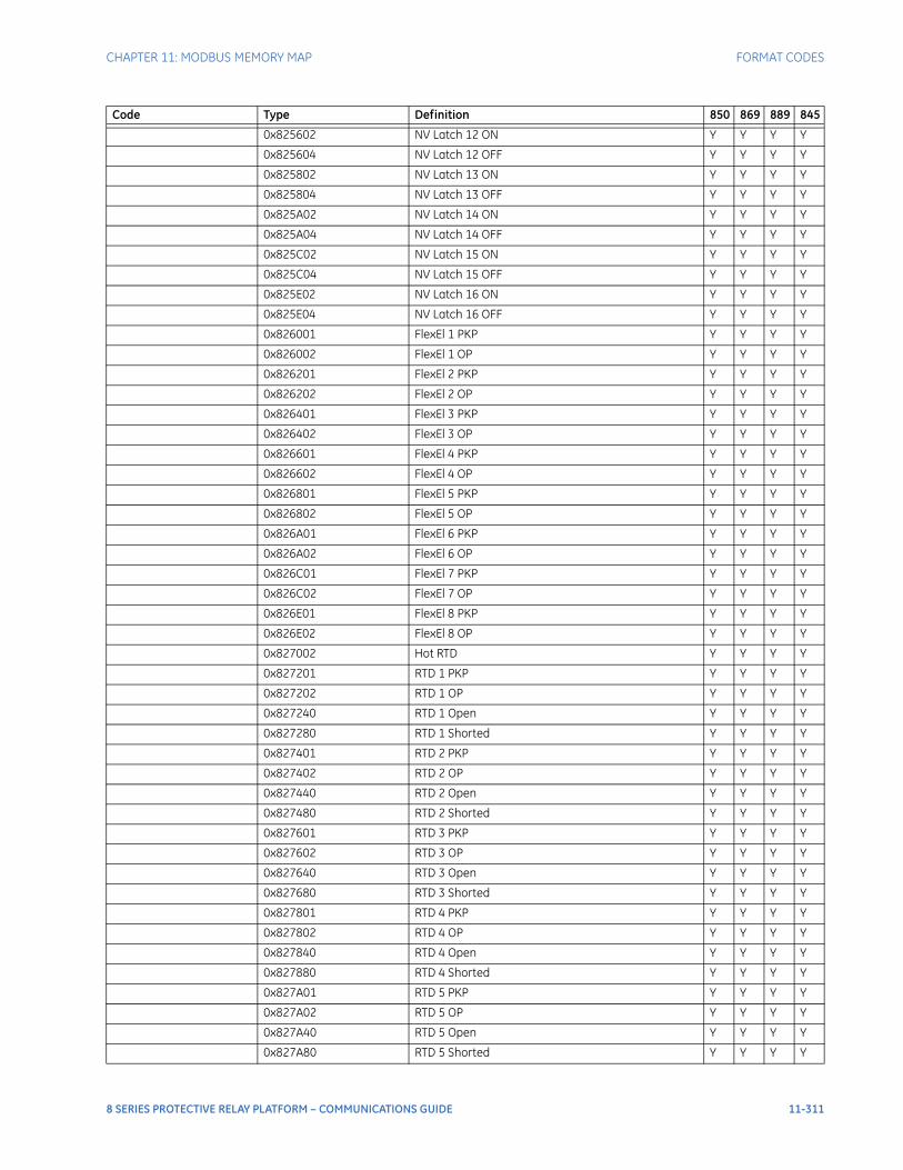
CHAPTER 11: MODBUS MEMORY MAP FORMAT CODES
0x825602 NV Latch 12 ON Y Y Y Y
0x825604 NV Latch 12 OFF Y Y Y Y
0x825802 NV Latch 13 ON Y Y Y Y
0x825804 NV Latch 13 OFF Y Y Y Y
0x825A02 NV Latch 14 ON Y Y Y Y
0x825A04 NV Latch 14 OFF Y Y Y Y
0x825C02 NV Latch 15 ON Y Y Y Y
0x825C04 NV Latch 15 OFF Y Y Y Y
0x825E02 NV Latch 16 ON Y Y Y Y
0x825E04 NV Latch 16 OFF Y Y Y Y
0x826001 FlexEl 1 PKP Y Y Y Y
0x826002 FlexEl 1 OP Y Y Y Y
0x826201 FlexEl 2 PKP Y Y Y Y
0x826202 FlexEl 2 OP Y Y Y Y
0x826401 FlexEl 3 PKP Y Y Y Y
0x826402 FlexEl 3 OP Y Y Y Y
0x826601 FlexEl 4 PKP Y Y Y Y
0x826602 FlexEl 4 OP Y Y Y Y
0x826801 FlexEl 5 PKP Y Y Y Y
0x826802 FlexEl 5 OP Y Y Y Y
0x826A01 FlexEl 6 PKP Y Y Y Y
0x826A02 FlexEl 6 OP Y Y Y Y
0x826C01 FlexEl 7 PKP Y Y Y Y
0x826C02 FlexEl 7 OP Y Y Y Y
0x826E01 FlexEl 8 PKP Y Y Y Y
0x826E02 FlexEl 8 OP Y Y Y Y
0x827002 Hot RTD Y Y Y Y
0x827201 RTD 1 PKP Y Y Y Y
0x827202 RTD 1 OP Y Y Y Y
0x827240 RTD 1 Open Y Y Y Y
0x827280 RTD 1 Shorted Y Y Y Y
0x827401 RTD 2 PKP Y Y Y Y
0x827402 RTD 2 OP Y Y Y Y
0x827440 RTD 2 Open Y Y Y Y
0x827480 RTD 2 Shorted Y Y Y Y
0x827601 RTD 3 PKP Y Y Y Y
0x827602 RTD 3 OP Y Y Y Y
0x827640 RTD 3 Open Y Y Y Y
0x827680 RTD 3 Shorted Y Y Y Y
0x827801 RTD 4 PKP Y Y Y Y
0x827802 RTD 4 OP Y Y Y Y
0x827840 RTD 4 Open Y Y Y Y
0x827880 RTD 4 Shorted Y Y Y Y
0x827A01 RTD 5 PKP Y Y Y Y
0x827A02 RTD 5 OP Y Y Y Y
0x827A40 RTD 5 Open Y Y Y Y
0x827A80 RTD 5 Shorted Y Y Y Y
Code Type Definition 850 869 889 845
8 SERIES PROTECTIVE RELAY PLATFORM – COMMUNICATIONS GUIDE 11-311
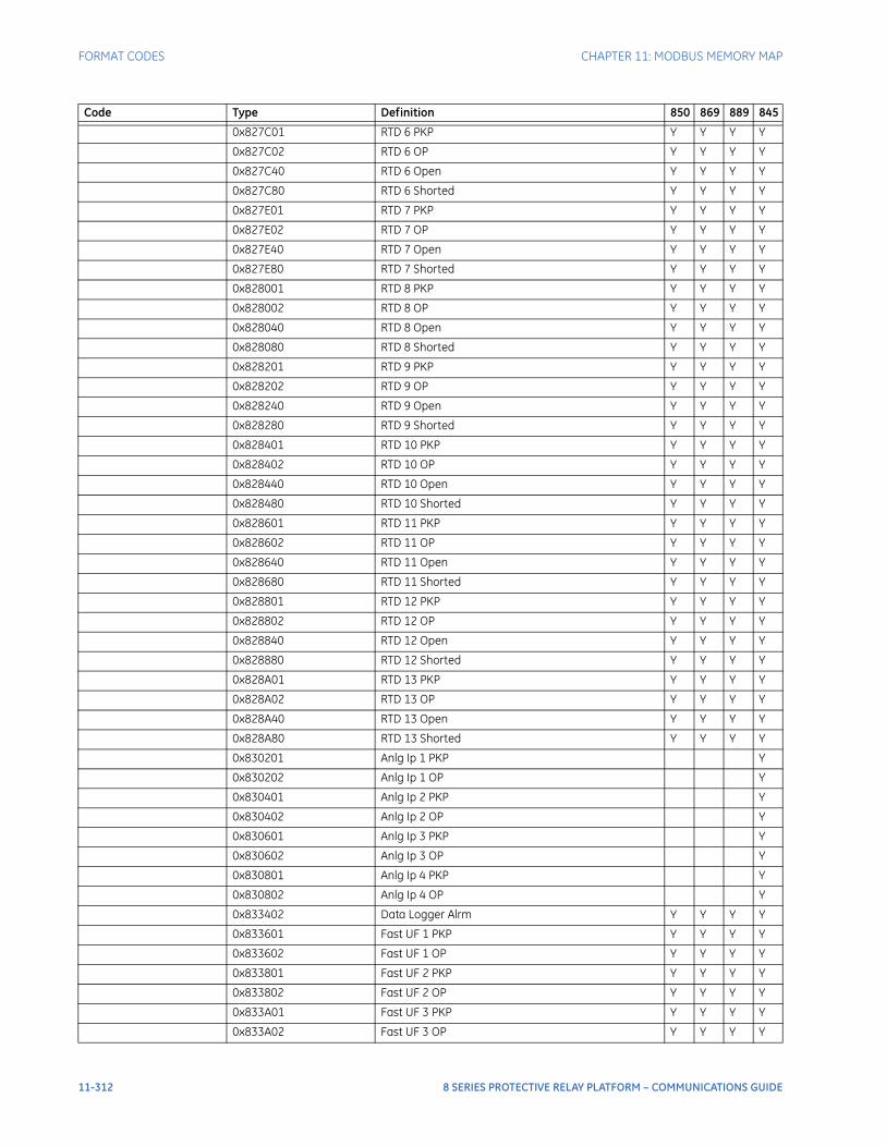
FORMAT CODES CHAPTER 11: MODBUS MEMORY MAP
0x827C01 RTD 6 PKP Y Y Y Y
0x827C02 RTD 6 OP Y Y Y Y
0x827C40 RTD 6 Open Y Y Y Y
0x827C80 RTD 6 Shorted Y Y Y Y
0x827E01 RTD 7 PKP Y Y Y Y
0x827E02 RTD 7 OP Y Y Y Y
0x827E40 RTD 7 Open Y Y Y Y
0x827E80 RTD 7 Shorted Y Y Y Y
0x828001 RTD 8 PKP Y Y Y Y
0x828002 RTD 8 OP Y Y Y Y
0x828040 RTD 8 Open Y Y Y Y
0x828080 RTD 8 Shorted Y Y Y Y
0x828201 RTD 9 PKP Y Y Y Y
0x828202 RTD 9 OP Y Y Y Y
0x828240 RTD 9 Open Y Y Y Y
0x828280 RTD 9 Shorted Y Y Y Y
0x828401 RTD 10 PKP Y Y Y Y
0x828402 RTD 10 OP Y Y Y Y
0x828440 RTD 10 Open Y Y Y Y
0x828480 RTD 10 Shorted Y Y Y Y
0x828601 RTD 11 PKP Y Y Y Y
0x828602 RTD 11 OP Y Y Y Y
0x828640 RTD 11 Open Y Y Y Y
0x828680 RTD 11 Shorted Y Y Y Y
0x828801 RTD 12 PKP Y Y Y Y
0x828802 RTD 12 OP Y Y Y Y
0x828840 RTD 12 Open Y Y Y Y
0x828880 RTD 12 Shorted Y Y Y Y
0x828A01 RTD 13 PKP Y Y Y Y
0x828A02 RTD 13 OP Y Y Y Y
0x828A40 RTD 13 Open Y Y Y Y
0x828A80 RTD 13 Shorted Y Y Y Y
0x830201 Anlg Ip 1 PKP Y
0x830202 Anlg Ip 1 OP Y
0x830401 Anlg Ip 2 PKP Y
0x830402 Anlg Ip 2 OP Y
0x830601 Anlg Ip 3 PKP Y
0x830602 Anlg Ip 3 OP Y
0x830801 Anlg Ip 4 PKP Y
0x830802 Anlg Ip 4 OP Y
0x833402 Data Logger Alrm Y Y Y Y
0x833601 Fast UF 1 PKP Y Y Y Y
0x833602 Fast UF 1 OP Y Y Y Y
0x833801 Fast UF 2 PKP Y Y Y Y
0x833802 Fast UF 2 OP Y Y Y Y
0x833A01 Fast UF 3 PKP Y Y Y Y
0x833A02 Fast UF 3 OP Y Y Y Y
Code Type Definition 850 869 889 845
11-312 8 SERIES PROTECTIVE RELAY PLATFORM – COMMUNICATIONS GUIDE
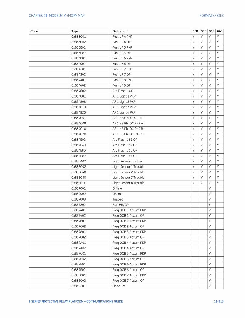
CHAPTER 11: MODBUS MEMORY MAP FORMAT CODES
0x833C01 Fast UF 4 PKP Y Y Y Y
0x833C02 Fast UF 4 OP Y Y Y Y
0x833E01 Fast UF 5 PKP Y Y Y Y
0x833E02 Fast UF 5 OP Y Y Y Y
0x834001 Fast UF 6 PKP Y Y Y Y
0x834002 Fast UF 6 OP Y Y Y Y
0x834201 Fast UF 7 PKP Y Y Y Y
0x834202 Fast UF 7 OP Y Y Y Y
0x834401 Fast UF 8 PKP Y Y Y Y
0x834402 Fast UF 8 OP Y Y Y Y
0x834602 Arc Flash 1 OP Y Y Y Y
0x834801 AF 1 Light 1 PKP Y Y Y Y
0x834808 AF 1 Light 2 PKP Y Y Y Y
0x834810 AF 1 Light 3 PKP Y Y Y Y
0x834820 AF 1 Light 4 PKP Y Y Y Y
0x834C01 AF 1 HS GND IOC PKP Y Y Y Y
0x834C08 AF 1 HS Ph IOC PKP A Y Y Y Y
0x834C10 AF 1 HS Ph IOC PKP B Y Y Y Y
0x834C20 AF 1 HS Ph IOC PKP C Y Y Y Y
0x834E02 Arc Flash 1 S1 OP Y Y Y Y
0x834E40 Arc Flash 1 S2 OP Y Y Y Y
0x834E80 Arc Flash 1 S3 OP Y Y Y Y
0x834F00 Arc Flash 1 S4 OP Y Y Y Y
0x836A02 Light Sensor Trouble Y Y Y Y
0x836C02 Light Sensor 1 Trouble Y Y Y Y
0x836C40 Light Sensor 2 Trouble Y Y Y Y
0x836C80 Light Sensor 3 Trouble Y Y Y Y
0x836D00 Light Sensor 4 Trouble Y Y Y Y
0x837001 Offline Y
0x837002 Online Y
0x837008 Tripped Y
0x837202 Run Hrs OP Y
0x837401 Freq OOB 1 Accum PKP Y
0x837402 Freq OOB 1 Accum OP Y
0x837601 Freq OOB 2 Accum PKP Y
0x837602 Freq OOB 2 Accum OP Y
0x837801 Freq OOB 3 Accum PKP Y
0x837802 Freq OOB 3 Accum OP Y
0x837A01 Freq OOB 4 Accum PKP Y
0x837A02 Freq OOB 4 Accum OP Y
0x837C01 Freq OOB 5 Accum PKP Y
0x837C02 Freq OOB 5 Accum OP Y
0x837E01 Freq OOB 6 Accum PKP Y
0x837E02 Freq OOB 6 Accum OP Y
0x838001 Freq OOB 7 Accum PKP Y
0x838002 Freq OOB 7 Accum OP Y
0x838201 Unbal PKP Y
Code Type Definition 850 869 889 845
8 SERIES PROTECTIVE RELAY PLATFORM – COMMUNICATIONS GUIDE 11-313
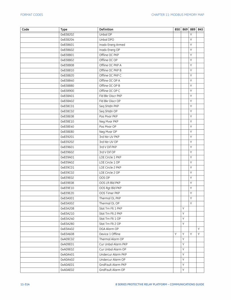
FORMAT CODES CHAPTER 11: MODBUS MEMORY MAP
0x838202 Unbal OP Y
0x838204 Unbal DPO Y
0x838601 Inadv Energ Armed Y
0x838602 Inadv Energ OP Y
0x838801 Offline OC PKP Y
0x838802 Offline OC OP Y
0x838808 Offline OC PKP A Y
0x838810 Offline OC PKP B Y
0x838820 Offline OC PKP C Y
0x838840 Offline OC OP A Y
0x838880 Offline OC OP B Y
0x838900 Offline OC OP C Y
0x838A01 Fld Bkr Discr PKP Y
0x838A02 Fld Bkr Discr OP Y
0x838C01 Seq Shtdn PKP Y
0x838C02 Seq Shtdn OP Y
0x838E08 Pos Mvar PKP Y
0x838E10 Neg Mvar PKP Y
0x838E40 Pos Mvar OP Y
0x838E80 Neg Mvar OP Y
0x839201 3rd Ntr UV PKP Y
0x839202 3rd Ntr UV OP Y
0x839601 3rd V Dif PKP Y
0x839602 3rd V Dif OP Y
0x839A01 LOE Circle 1 PKP Y
0x839A02 LOE Circle 1 OP Y
0x839C01 LOE Circle 2 PKP Y
0x839C02 LOE Circle 2 OP Y
0x839E02 OOS OP Y
0x839E08 OOS Lft Bld PKP Y
0x839E10 OOS Rgt Bld PKP Y
0x839E20 OOS Timer PKP Y
0x83A001 Thermal OL PKP Y
0x83A002 Thermal OL OP Y
0x83A208 Stat Trn Flt 1 PKP Y
0x83A210 Stat Trn Flt 2 PKP Y
0x83A240 Stat Trn Flt 1 OP Y
0x83A280 Stat Trn Flt 2 OP Y
0x83A402 DGA Alarm OP Y
0x83A608 Device 1 Offline Y Y Y Y
0xA09C02 Thermal Alarm OP Y
0xA09E01 Cur Unbal Alarm PKP Y
0xA09E02 Cur Unbal Alarm OP Y
0xA0A401 Undercur Alarm PKP Y
0xA0A402 Undercur Alarm OP Y
0xA0AE01 GndFault Alarm PKP Y
0xA0AE02 GndFault Alarm OP Y
Code Type Definition 850 869 889 845
11-314 8 SERIES PROTECTIVE RELAY PLATFORM – COMMUNICATIONS GUIDE
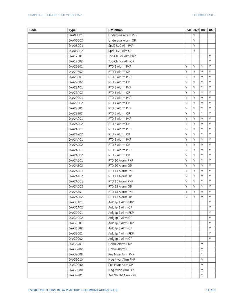
CHAPTER 11: MODBUS MEMORY MAP FORMAT CODES
0xA0B601 Underpwr Alarm PKP Y
0xA0B602 Underpwr Alarm OP Y
0xA0BC01 Spd2 U/C Alm PKP Y
0xA0BC02 Spd2 U/C Alm OP Y
0xA17E01 Tap Ch Fail Alm PKP Y
0xA17E02 Tap Ch Fail Alm OP Y
0xA29601 RTD 1 Alarm PKP Y Y Y Y
0xA29602 RTD 1 Alarm OP Y Y Y Y
0xA29801 RTD 2 Alarm PKP Y Y Y Y
0xA29802 RTD 2 Alarm OP Y Y Y Y
0xA29A01 RTD 3 Alarm PKP Y Y Y Y
0xA29A02 RTD 3 Alarm OP Y Y Y Y
0xA29C01 RTD 4 Alarm PKP Y Y Y Y
0xA29C02 RTD 4 Alarm OP Y Y Y Y
0xA29E01 RTD 5 Alarm PKP Y Y Y Y
0xA29E02 RTD 5 Alarm OP Y Y Y Y
0xA2A001 RTD 6 Alarm PKP Y Y Y Y
0xA2A002 RTD 6 Alarm OP Y Y Y Y
0xA2A201 RTD 7 Alarm PKP Y Y Y Y
0xA2A202 RTD 7 Alarm OP Y Y Y Y
0xA2A401 RTD 8 Alarm PKP Y Y Y Y
0xA2A402 RTD 8 Alarm OP Y Y Y Y
0xA2A601 RTD 9 Alarm PKP Y Y Y Y
0xA2A602 RTD 9 Alarm OP Y Y Y Y
0xA2A801 RTD 10 Alarm PKP Y Y Y Y
0xA2A802 RTD 10 Alarm OP Y Y Y Y
0xA2AA01 RTD 11 Alarm PKP Y Y Y Y
0xA2AA02 RTD 11 Alarm OP Y Y Y Y
0xA2AC01 RTD 12 Alarm PKP Y Y Y Y
0xA2AC02 RTD 12 Alarm OP Y Y Y Y
0xA2AE01 RTD 13 Alarm PKP Y Y Y Y
0xA2AE02 RTD 13 Alarm OP Y Y Y Y
0xA31A01 Anlg Ip 1 Alrm PKP Y
0xA31A02 Anlg Ip 1 Alrm OP Y
0xA31C01 Anlg Ip 2 Alrm PKP Y
0xA31C02 Anlg Ip 2 Alrm OP Y
0xA31E01 Anlg Ip 3 Alrm PKP Y
0xA31E02 Anlg Ip 3 Alrm OP Y
0xA32001 Anlg Ip 4 Alrm PKP Y
0xA32002 Anlg Ip 4 Alrm OP Y
0xA38401 Unbal Alarm PKP Y
0xA38402 Unbal Alarm OP Y
0xA39008 Pos Mvar Alrm PKP Y
0xA39010 Neg Mvar Alrm PKP Y
0xA39040 Pos Mvar Alrm OP Y
0xA39080 Neg Mvar Alrm OP Y
0xA39401 3rd Ntr UV Alrm PKP Y
Code Type Definition 850 869 889 845
8 SERIES PROTECTIVE RELAY PLATFORM – COMMUNICATIONS GUIDE 11-315
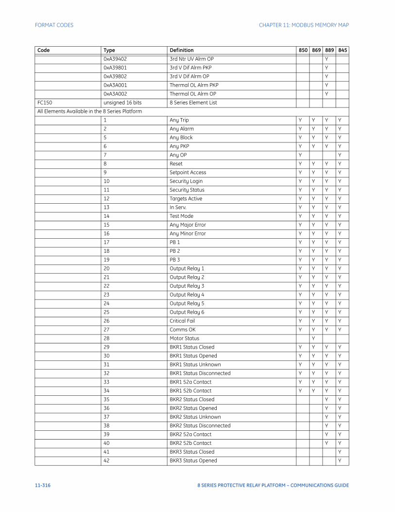
FORMAT CODES CHAPTER 11: MODBUS MEMORY MAP
0xA39402 3rd Ntr UV Alrm OP Y
0xA39801 3rd V Dif Alrm PKP Y
0xA39802 3rd V Dif Alrm OP Y
0xA3A001 Thermal OL Alrm PKP Y
0xA3A002 Thermal OL Alrm OP Y
FC150 unsigned 16 bits 8 Series Element List
All Elements Available in the 8 Series Platform
1 Any Trip Y Y Y Y
2 Any Alarm Y Y Y Y
5 Any Block Y Y Y Y
6 Any PKP Y Y Y Y
7 Any OP Y Y
8 Reset Y Y Y Y
9 Setpoint Access Y Y Y Y
10 Security Login Y Y Y Y
11 Security Status Y Y Y Y
12 Targets Active Y Y Y Y
13 In Serv. Y Y Y Y
14 Test Mode Y Y Y Y
15 Any Major Error Y Y Y Y
16 Any Minor Error Y Y Y Y
17 PB 1 Y Y Y Y
18 PB 2 Y Y Y Y
19 PB 3 Y Y Y Y
20 Output Relay 1 Y Y Y Y
21 Output Relay 2 Y Y Y Y
22 Output Relay 3 Y Y Y Y
23 Output Relay 4 Y Y Y Y
24 Output Relay 5 Y Y Y Y
25 Output Relay 6 Y Y Y Y
26 Critical Fail Y Y Y Y
27 Comms OK Y Y Y Y
28 Motor Status Y
29 BKR1 Status Closed Y Y Y Y
30 BKR1 Status Opened Y Y Y Y
31 BKR1 Status Unknown Y Y Y Y
32 BKR1 Status Disconnected Y Y Y Y
33 BKR1 52a Contact Y Y Y Y
34 BKR1 52b Contact Y Y Y Y
35 BKR2 Status Closed Y Y
36 BKR2 Status Opened Y Y
37 BKR2 Status Unknown Y Y
38 BKR2 Status Disconnected Y Y
39 BKR2 52a Contact Y Y
40 BKR2 52b Contact Y Y
41 BKR3 Status Closed Y
42 BKR3 Status Opened Y
Code Type Definition 850 869 889 845
11-316 8 SERIES PROTECTIVE RELAY PLATFORM – COMMUNICATIONS GUIDE
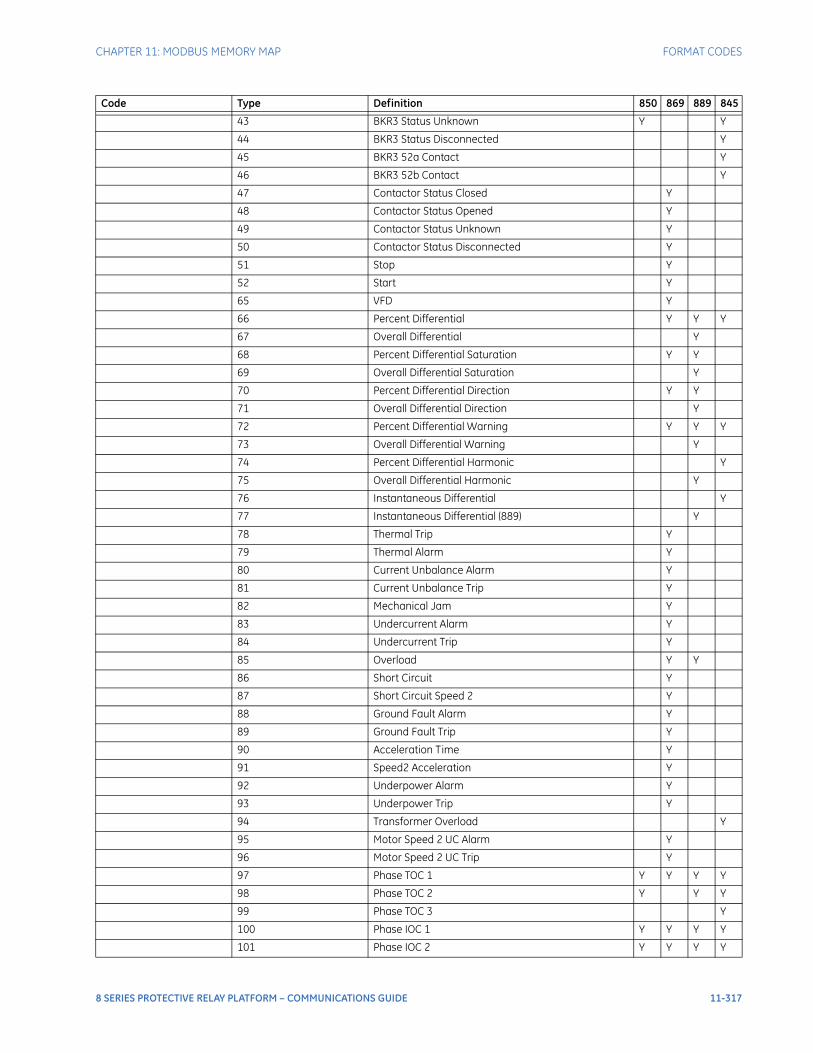
CHAPTER 11: MODBUS MEMORY MAP FORMAT CODES
43 BKR3 Status Unknown Y Y
44 BKR3 Status Disconnected Y
45 BKR3 52a Contact Y
46 BKR3 52b Contact Y
47 Contactor Status Closed Y
48 Contactor Status Opened Y
49 Contactor Status Unknown Y
50 Contactor Status Disconnected Y
51 Stop Y
52 Start Y
65 VFD Y
66 Percent Differential Y Y Y
67 Overall Differential Y
68 Percent Differential Saturation Y Y
69 Overall Differential Saturation Y
70 Percent Differential Direction Y Y
71 Overall Differential Direction Y
72 Percent Differential Warning Y Y Y
73 Overall Differential Warning Y
74 Percent Differential Harmonic Y
75 Overall Differential Harmonic Y
76 Instantaneous Differential Y
77 Instantaneous Differential (889) Y
78 Thermal Trip Y
79 Thermal Alarm Y
80 Current Unbalance Alarm Y
81 Current Unbalance Trip Y
82 Mechanical Jam Y
83 Undercurrent Alarm Y
84 Undercurrent Trip Y
85 Overload Y Y
86 Short Circuit Y
87 Short Circuit Speed 2 Y
88 Ground Fault Alarm Y
89 Ground Fault Trip Y
90 Acceleration Time Y
91 Speed2 Acceleration Y
92 Underpower Alarm Y
93 Underpower Trip Y
94 Transformer Overload Y
95 Motor Speed 2 UC Alarm Y
96 Motor Speed 2 UC Trip Y
97 Phase TOC 1 Y Y Y Y
98 Phase TOC 2 Y Y Y
99 Phase TOC 3 Y
100 Phase IOC 1 Y Y Y Y
101 Phase IOC 2 Y Y Y Y
Code Type Definition 850 869 889 845
8 SERIES PROTECTIVE RELAY PLATFORM – COMMUNICATIONS GUIDE 11-317
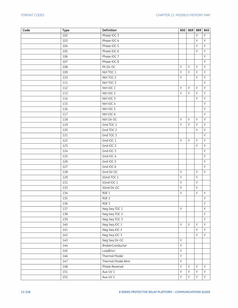
FORMAT CODES CHAPTER 11: MODBUS MEMORY MAP
102 Phase IOC 3 Y Y
103 Phase IOC 4 Y Y
104 Phase IOC 5 Y Y
105 Phase IOC 6 Y Y
106 Phase IOC 7 Y
107 Phase IOC 8 Y
108 Ph Dir OC Y Y Y Y
109 Ntrl TOC 1 Y Y Y Y
110 Ntrl TOC 2 Y Y Y
111 Ntrl TOC 3 Y
112 Ntrl IOC 1 Y Y Y Y
113 Ntrl IOC 2 Y Y Y Y
114 Ntrl IOC 3 Y Y
115 Ntrl IOC 4 Y
116 Ntrl IOC 5 Y
117 Ntrl IOC 6 Y
118 Ntrl Dir OC Y Y Y Y
119 Gnd TOC 1 Y Y Y Y
120 Gnd TOC 2 Y Y
121 Gnd TOC 3 Y
122 Gnd IOC 1 Y Y Y Y
123 Gnd IOC 2 Y Y
124 Gnd IOC 3 Y
125 Gnd IOC 4 Y
126 Gnd IOC 5 Y
127 Gnd IOC 6 Y
128 Gnd Dir OC Y Y Y
129 SGnd TOC 1 Y Y
131 SGnd IOC 1 Y Y
133 SGnd Dir OC Y Y
134 RGF 1 Y Y Y
135 RGF 2 Y
136 RGF 3 Y
137 Neg Seq TOC 1 Y Y
138 Neg Seq TOC 2 Y
139 Neg Seq TOC 3 Y
140 Neg Seq IOC 1 Y Y Y Y
141 Neg Seq IOC 2 Y Y
142 Neg Seq IOC 3 Y Y
143 Neg Seq Dir OC Y
144 BrokenConductor Y
145 LoadEncr Y
146 Thermal Model Y
147 Thermal Model Alrm Y
148 Phase Reversal Y Y Y Y
151 Aux UV 1 Y Y Y Y
152 Aux UV 2 Y Y Y Y
Code Type Definition 850 869 889 845
11-318 8 SERIES PROTECTIVE RELAY PLATFORM – COMMUNICATIONS GUIDE
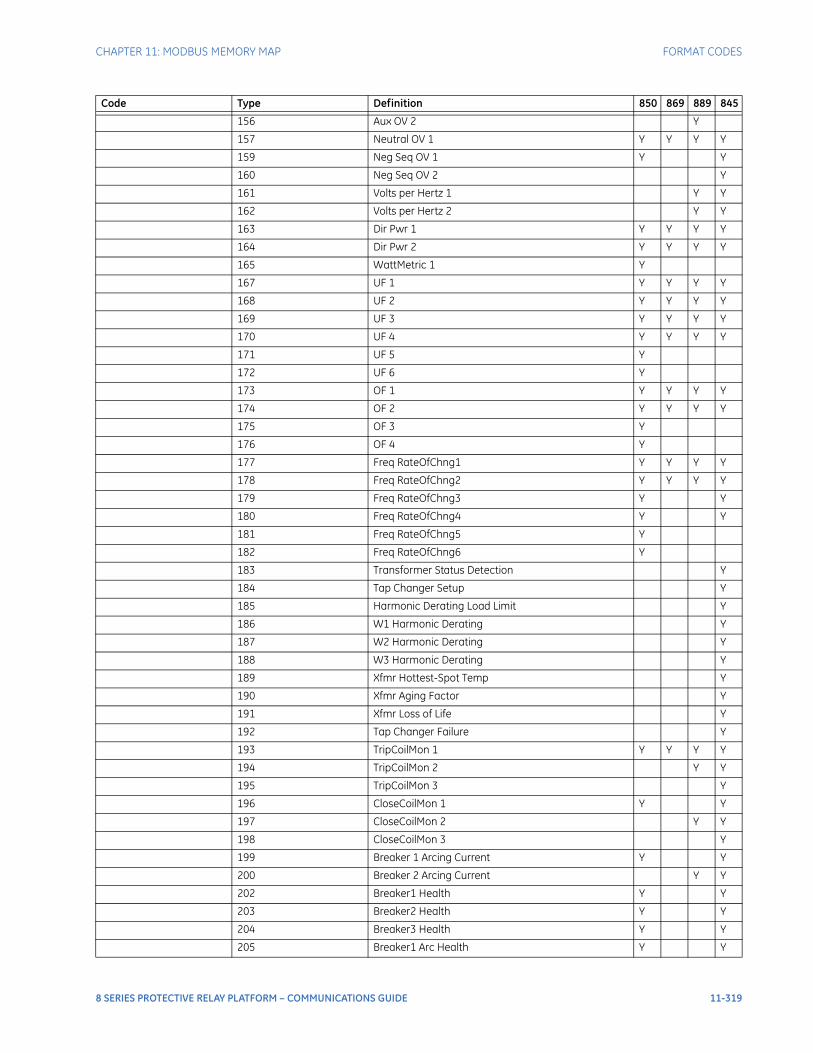
CHAPTER 11: MODBUS MEMORY MAP FORMAT CODES
156 Aux OV 2 Y
157 Neutral OV 1 Y Y Y Y
159 Neg Seq OV 1 Y Y
160 Neg Seq OV 2 Y
161 Volts per Hertz 1 Y Y
162 Volts per Hertz 2 Y Y
163 Dir Pwr 1 Y Y Y Y
164 Dir Pwr 2 Y Y Y Y
165 WattMetric 1 Y
167 UF 1 Y Y Y Y
168 UF 2 Y Y Y Y
169 UF 3 Y Y Y Y
170 UF 4 Y Y Y Y
171 UF 5 Y
172 UF 6 Y
173 OF 1 Y Y Y Y
174 OF 2 Y Y Y Y
175 OF 3 Y
176 OF 4 Y
177 Freq RateOfChng1 Y Y Y Y
178 Freq RateOfChng2 Y Y Y Y
179 Freq RateOfChng3 Y Y
180 Freq RateOfChng4 Y Y
181 Freq RateOfChng5 Y
182 Freq RateOfChng6 Y
183 Transformer Status Detection Y
184 Tap Changer Setup Y
185 Harmonic Derating Load Limit Y
186 W1 Harmonic Derating Y
187 W2 Harmonic Derating Y
188 W3 Harmonic Derating Y
189 Xfmr Hottest-Spot Temp Y
190 Xfmr Aging Factor Y
191 Xfmr Loss of Life Y
192 Tap Changer Failure Y
193 TripCoilMon 1 Y Y Y Y
194 TripCoilMon 2 Y Y
195 TripCoilMon 3 Y
196 CloseCoilMon 1 Y Y
197 CloseCoilMon 2 Y Y
198 CloseCoilMon 3 Y
199 Breaker 1 Arcing Current Y Y
200 Breaker 2 Arcing Current Y Y
202 Breaker1 Health Y Y
203 Breaker2 Health Y Y
204 Breaker3 Health Y Y
205 Breaker1 Arc Health Y Y
Code Type Definition 850 869 889 845
8 SERIES PROTECTIVE RELAY PLATFORM – COMMUNICATIONS GUIDE 11-319
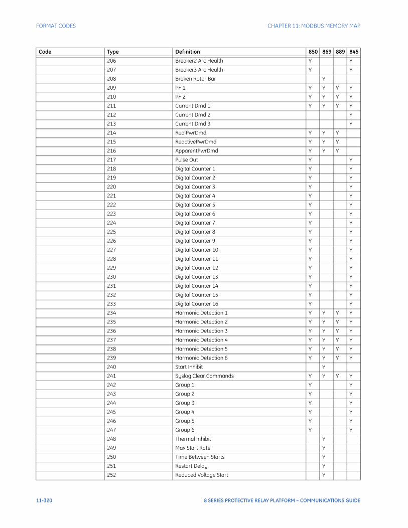
FORMAT CODES CHAPTER 11: MODBUS MEMORY MAP
206 Breaker2 Arc Health Y Y
207 Breaker3 Arc Health Y Y
208 Broken Rotor Bar Y
209 PF 1 Y Y Y Y
210 PF 2 Y Y Y Y
211 Current Dmd 1 Y Y Y Y
212 Current Dmd 2 Y
213 Current Dmd 3 Y
214 RealPwrDmd Y Y Y
215 ReactivePwrDmd Y Y Y
216 ApparentPwrDmd Y Y Y
217 Pulse Out Y Y
218 Digital Counter 1 Y Y
219 Digital Counter 2 Y Y
220 Digital Counter 3 Y Y
221 Digital Counter 4 Y Y
222 Digital Counter 5 Y Y
223 Digital Counter 6 Y Y
224 Digital Counter 7 Y Y
225 Digital Counter 8 Y Y
226 Digital Counter 9 Y Y
227 Digital Counter 10 Y Y
228 Digital Counter 11 Y Y
229 Digital Counter 12 Y Y
230 Digital Counter 13 Y Y
231 Digital Counter 14 Y Y
232 Digital Counter 15 Y Y
233 Digital Counter 16 Y Y
234 Harmonic Detection 1 Y Y Y Y
235 Harmonic Detection 2 Y Y Y Y
236 Harmonic Detection 3 Y Y Y Y
237 Harmonic Detection 4 Y Y Y Y
238 Harmonic Detection 5 Y Y Y Y
239 Harmonic Detection 6 Y Y Y Y
240 Start Inhibit Y
241 Syslog Clear Commands Y Y Y Y
242 Group 1 Y Y
243 Group 2 Y Y
244 Group 3 Y Y
245 Group 4 Y Y
246 Group 5 Y Y
247 Group 6 Y Y
248 Thermal Inhibit Y
249 Max Start Rate Y
250 Time Between Starts Y
251 Restart Delay Y
252 Reduced Voltage Start Y
Code Type Definition 850 869 889 845
11-320 8 SERIES PROTECTIVE RELAY PLATFORM – COMMUNICATIONS GUIDE

CHAPTER 11: MODBUS MEMORY MAP FORMAT CODES
253 Reduced Voltage Fail Y
254 Local Mode Y Y Y
255 Open BKR 1 Y Y
256 Open BKR 2 Y Y
258 Close BKR 1 Y Y
259 Close BKR 2 Y Y
261 Trip Bus 1 Y Y
262 Trip Bus 2 Y Y
263 Trip Bus 3 Y Y
264 Trip Bus 4 Y Y
265 Trip Bus 5 Y Y
266 Trip Bus 6 Y Y
267 BKR Fail 1 Y Y
268 BKR Fail 2 Y Y
269 BKR Fail 3 Y
270 Sync Check 1 Y Y Y
272 Manual Cls Blk Y
273 CLP 1 Y
275 UV Restore Y
276 UF Restore Y
277 Bus Transfer Y
278 Transfer Initiated Y
279 AR1 Y
280 AR1 Shot Cnt Y
281 AR1 Shot Cnt Reduction Y
282 AR1 Rate Supervision Y
287 VTFF 1 Y Y
289 NV Latch 1 Y Y
290 NV Latch 2 Y Y
291 NV Latch 3 Y Y
292 NV Latch 4 Y Y
293 NV Latch 5 Y Y
294 NV Latch 6 Y Y
295 NV Latch 7 Y Y
296 NV Latch 8 Y Y
297 NV Latch 9 Y Y
298 NV Latch 10 Y Y
299 NV Latch 11 Y Y
300 NV Latch 12 Y Y
301 NV Latch 13 Y Y
302 NV Latch 14 Y Y
303 NV Latch 15 Y Y
304 NV Latch 16 Y Y
305 FlexElement 1 Y Y Y Y
306 FlexElement 2 Y Y Y Y
307 FlexElement 3 Y Y Y Y
308 FlexElement 4 Y Y Y Y
Code Type Definition 850 869 889 845
8 SERIES PROTECTIVE RELAY PLATFORM – COMMUNICATIONS GUIDE 11-321
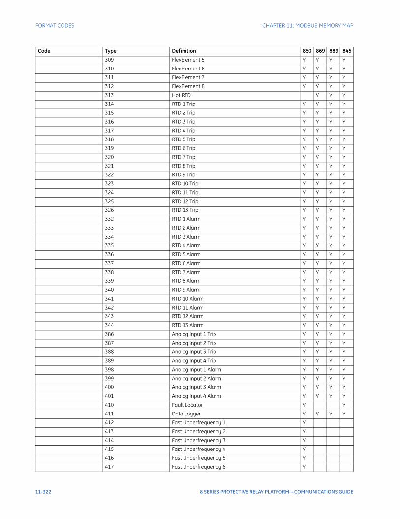
FORMAT CODES CHAPTER 11: MODBUS MEMORY MAP
309 FlexElement 5 Y Y Y Y
310 FlexElement 6 Y Y Y Y
311 FlexElement 7 Y Y Y Y
312 FlexElement 8 Y Y Y Y
313 Hot RTD Y Y Y
314 RTD 1 Trip Y Y Y Y
315 RTD 2 Trip Y Y Y Y
316 RTD 3 Trip Y Y Y Y
317 RTD 4 Trip Y Y Y Y
318 RTD 5 Trip Y Y Y Y
319 RTD 6 Trip Y Y Y Y
320 RTD 7 Trip Y Y Y Y
321 RTD 8 Trip Y Y Y Y
322 RTD 9 Trip Y Y Y Y
323 RTD 10 Trip Y Y Y Y
324 RTD 11 Trip Y Y Y Y
325 RTD 12 Trip Y Y Y Y
326 RTD 13 Trip Y Y Y Y
332 RTD 1 Alarm Y Y Y Y
333 RTD 2 Alarm Y Y Y Y
334 RTD 3 Alarm Y Y Y Y
335 RTD 4 Alarm Y Y Y Y
336 RTD 5 Alarm Y Y Y Y
337 RTD 6 Alarm Y Y Y Y
338 RTD 7 Alarm Y Y Y Y
339 RTD 8 Alarm Y Y Y Y
340 RTD 9 Alarm Y Y Y Y
341 RTD 10 Alarm Y Y Y Y
342 RTD 11 Alarm Y Y Y Y
343 RTD 12 Alarm Y Y Y Y
344 RTD 13 Alarm Y Y Y Y
386 Analog Input 1 Trip Y Y Y Y
387 Analog Input 2 Trip Y Y Y Y
388 Analog Input 3 Trip Y Y Y Y
389 Analog Input 4 Trip Y Y Y Y
398 Analog Input 1 Alarm Y Y Y Y
399 Analog Input 2 Alarm Y Y Y Y
400 Analog Input 3 Alarm Y Y Y Y
401 Analog Input 4 Alarm Y Y Y Y
410 Fault Locator Y Y
411 Data Logger Y Y Y Y
412 Fast Underfrequency 1 Y
413 Fast Underfrequency 2 Y
414 Fast Underfrequency 3 Y
415 Fast Underfrequency 4 Y
416 Fast Underfrequency 5 Y
417 Fast Underfrequency 6 Y
Code Type Definition 850 869 889 845
11-322 8 SERIES PROTECTIVE RELAY PLATFORM – COMMUNICATIONS GUIDE
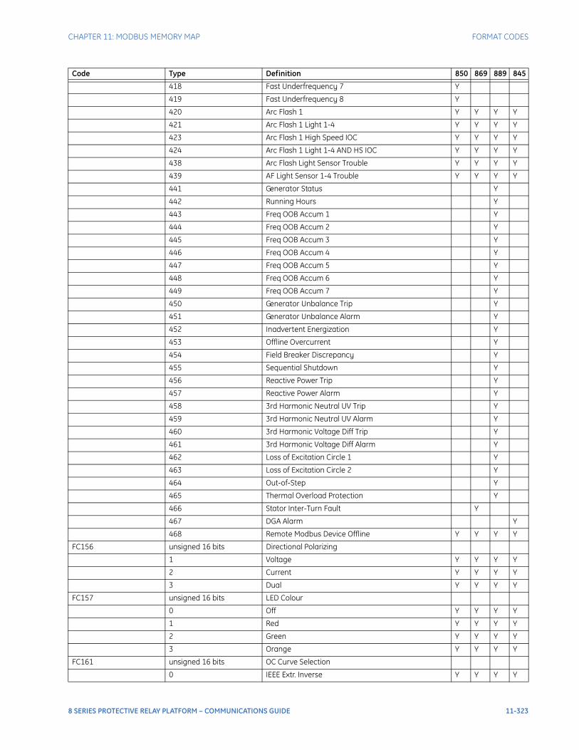
CHAPTER 11: MODBUS MEMORY MAP FORMAT CODES
418 Fast Underfrequency 7 Y
419 Fast Underfrequency 8 Y
420 Arc Flash 1 Y Y Y Y
421 Arc Flash 1 Light 1-4 Y Y Y Y
423 Arc Flash 1 High Speed IOC Y Y Y Y
424 Arc Flash 1 Light 1-4 AND HS IOC Y Y Y Y
438 Arc Flash Light Sensor Trouble Y Y Y Y
439 AF Light Sensor 1-4 Trouble Y Y Y Y
441 Generator Status Y
442 Running Hours Y
443 Freq OOB Accum 1 Y
444 Freq OOB Accum 2 Y
445 Freq OOB Accum 3 Y
446 Freq OOB Accum 4 Y
447 Freq OOB Accum 5 Y
448 Freq OOB Accum 6 Y
449 Freq OOB Accum 7 Y
450 Generator Unbalance Trip Y
451 Generator Unbalance Alarm Y
452 Inadvertent Energization Y
453 Offline Overcurrent Y
454 Field Breaker Discrepancy Y
455 Sequential Shutdown Y
456 Reactive Power Trip Y
457 Reactive Power Alarm Y
458 3rd Harmonic Neutral UV Trip Y
459 3rd Harmonic Neutral UV Alarm Y
460 3rd Harmonic Voltage Diff Trip Y
461 3rd Harmonic Voltage Diff Alarm Y
462 Loss of Excitation Circle 1 Y
463 Loss of Excitation Circle 2 Y
464 Out-of-Step Y
465 Thermal Overload Protection Y
466 Stator Inter-Turn Fault Y
467 DGA Alarm Y
468 Remote Modbus Device Offline Y Y Y Y
FC156 unsigned 16 bits Directional Polarizing
1 Voltage Y Y Y Y
2 Current Y Y Y Y
3 Dual Y Y Y Y
FC157 unsigned 16 bits LED Colour
0 Off Y Y Y Y
1 Red Y Y Y Y
2 Green Y Y Y Y
3 Orange Y Y Y Y
FC161 unsigned 16 bits OC Curve Selection
0 IEEE Extr. Inverse Y Y Y Y
Code Type Definition 850 869 889 845
8 SERIES PROTECTIVE RELAY PLATFORM – COMMUNICATIONS GUIDE 11-323
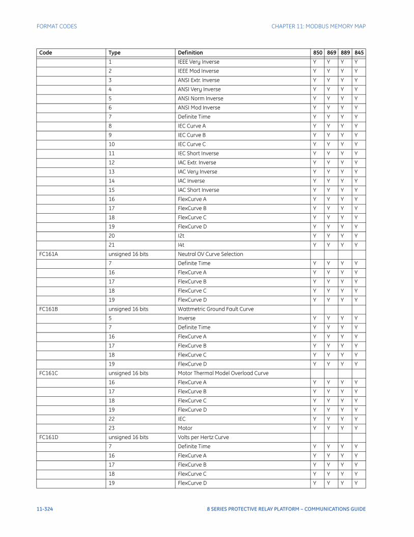
FORMAT CODES CHAPTER 11: MODBUS MEMORY MAP
1 IEEE Very Inverse Y Y Y Y
2 IEEE Mod Inverse Y Y Y Y
3 ANSI Extr. Inverse Y Y Y Y
4 ANSI Very Inverse Y Y Y Y
5 ANSI Norm Inverse Y Y Y Y
6 ANSI Mod Inverse Y Y Y Y
7 Definite Time Y Y Y Y
8 IEC Curve A Y Y Y Y
9 IEC Curve B Y Y Y Y
10 IEC Curve C Y Y Y Y
11 IEC Short Inverse Y Y Y Y
12 IAC Extr. Inverse Y Y Y Y
13 IAC Very Inverse Y Y Y Y
14 IAC Inverse Y Y Y Y
15 IAC Short Inverse Y Y Y Y
16 FlexCurve A Y Y Y Y
17 FlexCurve B Y Y Y Y
18 FlexCurve C Y Y Y Y
19 FlexCurve D Y Y Y Y
20 I2t Y Y Y Y
21 I4t Y Y Y Y
FC161A unsigned 16 bits Neutral OV Curve Selection
7 Definite Time Y Y Y Y
16 FlexCurve A Y Y Y Y
17 FlexCurve B Y Y Y Y
18 FlexCurve C Y Y Y Y
19 FlexCurve D Y Y Y Y
FC161B unsigned 16 bits Wattmetric Ground Fault Curve
5 Inverse Y Y Y Y
7 Definite Time Y Y Y Y
16 FlexCurve A Y Y Y Y
17 FlexCurve B Y Y Y Y
18 FlexCurve C Y Y Y Y
19 FlexCurve D Y Y Y Y
FC161C unsigned 16 bits Motor Thermal Model Overload Curve
16 FlexCurve A Y Y Y Y
17 FlexCurve B Y Y Y Y
18 FlexCurve C Y Y Y Y
19 FlexCurve D Y Y Y Y
22 IEC Y Y Y Y
23 Motor Y Y Y Y
FC161D unsigned 16 bits Volts per Hertz Curve
7 Definite Time Y Y Y Y
16 FlexCurve A Y Y Y Y
17 FlexCurve B Y Y Y Y
18 FlexCurve C Y Y Y Y
19 FlexCurve D Y Y Y Y
Code Type Definition 850 869 889 845
11-324 8 SERIES PROTECTIVE RELAY PLATFORM – COMMUNICATIONS GUIDE
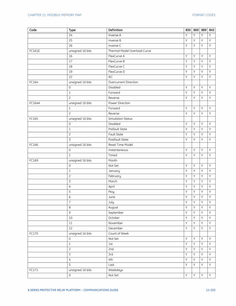
CHAPTER 11: MODBUS MEMORY MAP FORMAT CODES
24 Inverse A Y Y Y Y
25 Inverse B Y Y Y Y
26 Inverse C Y Y Y Y
FC161E unsigned 16 bits Thermal Model Overload Curve
16 FlexCurve A Y Y Y Y
17 FlexCurve B Y Y Y Y
18 FlexCurve C Y Y Y Y
19 FlexCurve D Y Y Y Y
22 IEC Y Y Y Y
FC164 unsigned 16 bits Overcurrent Direction
0 Disabled Y Y Y Y
1 Forward Y Y Y Y
2 Reverse Y Y Y Y
FC164A unsigned 16 bits Power Direction
1 Forward Y Y Y Y
2 Reverse Y Y Y Y
FC165 unsigned 16 bits Simulation Status
0 Disabled Y Y Y Y
1 Prefault State Y Y Y Y
2 Fault State Y Y Y Y
3 Postfault State Y Y Y Y
FC166 unsigned 16 bits Reset Time Model
0 Instantaneous Y Y Y Y
1 Timed Y Y Y Y
FC169 unsigned 16 bits Month
0 Not Set Y Y Y Y
1 January Y Y Y Y
2 February Y Y Y Y
3 March Y Y Y Y
4 April Y Y Y Y
5 May Y Y Y Y
6 June Y Y Y Y
7 July Y Y Y Y
8 August Y Y Y Y
9 September Y Y Y Y
10 October Y Y Y Y
11 November Y Y Y Y
12 December Y Y Y Y
FC170 unsigned 16 bits Count of Week
0 Not Set Y Y Y Y
1 1st Y Y Y Y
2 2nd Y Y Y Y
3 3rd Y Y Y Y
4 4th Y Y Y Y
5 Last Y Y Y Y
FC171 unsigned 16 bits Weekdays
0 Not Set Y Y Y Y
Code Type Definition 850 869 889 845
8 SERIES PROTECTIVE RELAY PLATFORM – COMMUNICATIONS GUIDE 11-325

FORMAT CODES CHAPTER 11: MODBUS MEMORY MAP
1 SUN Y Y Y Y
2 MON Y Y Y Y
3 TUE Y Y Y Y
4 WED Y Y Y Y
5 THU Y Y Y Y
6 FRI Y Y Y Y
7 SAT Y Y Y Y
FC176 unsigned 16 bits Auxiliary VT Connection
0 Vab VT Y Y Y Y
1 Vbc VT Y Y Y Y
2 Vca VT Y Y Y Y
3 Van VT Y Y Y Y
4 Vbn VT Y Y Y Y
5 Vcn VT Y Y Y Y
6 Vn Y Y Y Y
FC177 unsigned 16 bits
0 Auxiliary 52a Y Y Y Y
1 Auxiliary 52b Y Y Y Y
FC181 unsigned 16 bits Transient Recorder Trigger Mode
0 Overwrite Y Y Y Y
1 Protected Y Y Y Y
FC182 unsigned 16 bits Transient Recorder Samples Per Cycle
0 128 /c Y Y Y Y
1 64 /c Y Y Y Y
2 32 /c Y Y Y Y
3 16 /c Y Y Y Y
4 8 /c Y Y Y Y
FC183 unsigned 16 bits Data Logger Sample Rate
0 1 Cycle Y Y Y Y
1 1 Second Y Y Y Y
2 30 Seconds Y Y Y Y
3 1 Minute Y Y Y Y
4 15 Minutes Y Y Y Y
5 30 Minutes Y Y Y Y
6 1 Hour Y Y Y Y
FC186 unsigned 16 bits DataLogger Collection Mode
0 Disabled Y Y Y Y
1 Continuous Y Y Y Y
2 Triggered Y Y Y Y
FC187 unsigned 16 bits Data Logger Channel Mode
0 Sample Y Y Y Y
1 Max Y Y Y Y
2 Min Y Y Y Y
3 Mean Y Y Y Y
FC191 unsigned 32 bits Remote Input Operation
0x00000001 Remote Input 1 Y Y Y Y
0x00000002 Remote Input 2 Y Y Y Y
Code Type Definition 850 869 889 845
11-326 8 SERIES PROTECTIVE RELAY PLATFORM – COMMUNICATIONS GUIDE
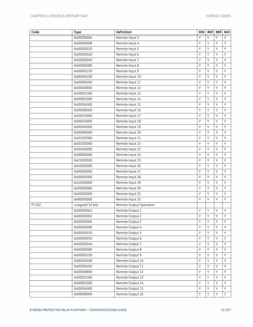
CHAPTER 11: MODBUS MEMORY MAP FORMAT CODES
0x00000004 Remote Input 3 Y Y Y Y
0x00000008 Remote Input 4 Y Y Y Y
0x00000010 Remote Input 5 Y Y Y Y
0x00000020 Remote Input 6 Y Y Y Y
0x00000040 Remote Input 7 Y Y Y Y
0x00000080 Remote Input 8 Y Y Y Y
0x00000100 Remote Input 9 Y Y Y Y
0x00000200 Remote Input 10 Y Y Y Y
0x00000400 Remote Input 11 Y Y Y Y
0x00000800 Remote Input 12 Y Y Y Y
0x00001000 Remote Input 13 Y Y Y Y
0x00002000 Remote Input 14 Y Y Y Y
0x00004000 Remote Input 15 Y Y Y Y
0x00008000 Remote Input 16 Y Y Y Y
0x00010000 Remote Input 17 Y Y Y Y
0x00020000 Remote Input 18 Y Y Y Y
0x00040000 Remote Input 19 Y Y Y Y
0x00080000 Remote Input 20 Y Y Y Y
0x00100000 Remote Input 21 Y Y Y Y
0x00200000 Remote Input 22 Y Y Y Y
0x00400000 Remote Input 23 Y Y Y Y
0x00800000 Remote Input 24 Y Y Y Y
0x01000000 Remote Input 25 Y Y Y Y
0x02000000 Remote Input 26 Y Y Y Y
0x04000000 Remote Input 27 Y Y Y Y
0x08000000 Remote Input 28 Y Y Y Y
0x10000000 Remote Input 29 Y Y Y Y
0x20000000 Remote Input 30 Y Y Y Y
0x40000000 Remote Input 31 Y Y Y Y
0x80000000 Remote Input 32 Y Y Y Y
FC192 unsigned 32 bits Remote Output Operation
0x00000001 Remote Output 1 Y Y Y Y
0x00000002 Remote Output 2 Y Y Y Y
0x00000004 Remote Output 3 Y Y Y Y
0x00000008 Remote Output 4 Y Y Y Y
0x00000010 Remote Output 5 Y Y Y Y
0x00000020 Remote Output 6 Y Y Y Y
0x00000040 Remote Output 7 Y Y Y Y
0x00000080 Remote Output 8 Y Y Y Y
0x00000100 Remote Output 9 Y Y Y Y
0x00000200 Remote Output 10 Y Y Y Y
0x00000400 Remote Output 11 Y Y Y Y
0x00000800 Remote Output 12 Y Y Y Y
0x00001000 Remote Output 13 Y Y Y Y
0x00002000 Remote Output 14 Y Y Y Y
0x00004000 Remote Output 15 Y Y Y Y
0x00008000 Remote Output 16 Y Y Y Y
Code Type Definition 850 869 889 845
8 SERIES PROTECTIVE RELAY PLATFORM – COMMUNICATIONS GUIDE 11-327
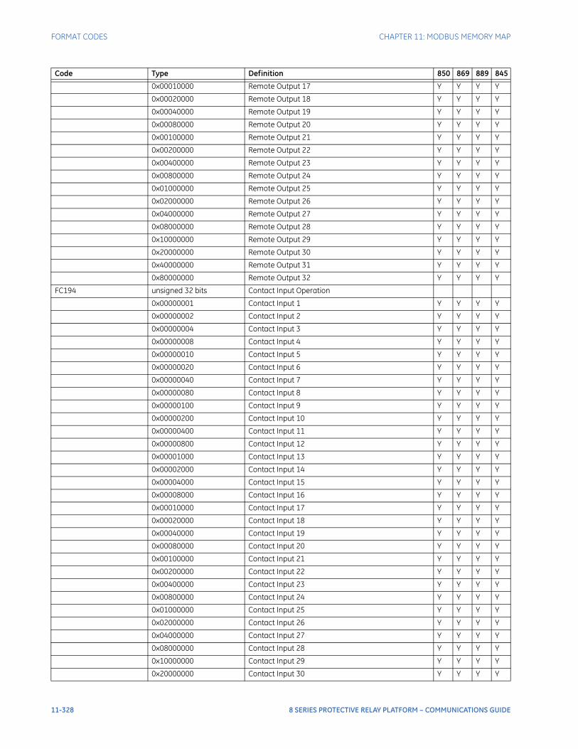
FORMAT CODES CHAPTER 11: MODBUS MEMORY MAP
0x00010000 Remote Output 17 Y Y Y Y
0x00020000 Remote Output 18 Y Y Y Y
0x00040000 Remote Output 19 Y Y Y Y
0x00080000 Remote Output 20 Y Y Y Y
0x00100000 Remote Output 21 Y Y Y Y
0x00200000 Remote Output 22 Y Y Y Y
0x00400000 Remote Output 23 Y Y Y Y
0x00800000 Remote Output 24 Y Y Y Y
0x01000000 Remote Output 25 Y Y Y Y
0x02000000 Remote Output 26 Y Y Y Y
0x04000000 Remote Output 27 Y Y Y Y
0x08000000 Remote Output 28 Y Y Y Y
0x10000000 Remote Output 29 Y Y Y Y
0x20000000 Remote Output 30 Y Y Y Y
0x40000000 Remote Output 31 Y Y Y Y
0x80000000 Remote Output 32 Y Y Y Y
FC194 unsigned 32 bits Contact Input Operation
0x00000001 Contact Input 1 Y Y Y Y
0x00000002 Contact Input 2 Y Y Y Y
0x00000004 Contact Input 3 Y Y Y Y
0x00000008 Contact Input 4 Y Y Y Y
0x00000010 Contact Input 5 Y Y Y Y
0x00000020 Contact Input 6 Y Y Y Y
0x00000040 Contact Input 7 Y Y Y Y
0x00000080 Contact Input 8 Y Y Y Y
0x00000100 Contact Input 9 Y Y Y Y
0x00000200 Contact Input 10 Y Y Y Y
0x00000400 Contact Input 11 Y Y Y Y
0x00000800 Contact Input 12 Y Y Y Y
0x00001000 Contact Input 13 Y Y Y Y
0x00002000 Contact Input 14 Y Y Y Y
0x00004000 Contact Input 15 Y Y Y Y
0x00008000 Contact Input 16 Y Y Y Y
0x00010000 Contact Input 17 Y Y Y Y
0x00020000 Contact Input 18 Y Y Y Y
0x00040000 Contact Input 19 Y Y Y Y
0x00080000 Contact Input 20 Y Y Y Y
0x00100000 Contact Input 21 Y Y Y Y
0x00200000 Contact Input 22 Y Y Y Y
0x00400000 Contact Input 23 Y Y Y Y
0x00800000 Contact Input 24 Y Y Y Y
0x01000000 Contact Input 25 Y Y Y Y
0x02000000 Contact Input 26 Y Y Y Y
0x04000000 Contact Input 27 Y Y Y Y
0x08000000 Contact Input 28 Y Y Y Y
0x10000000 Contact Input 29 Y Y Y Y
0x20000000 Contact Input 30 Y Y Y Y
Code Type Definition 850 869 889 845
11-328 8 SERIES PROTECTIVE RELAY PLATFORM – COMMUNICATIONS GUIDE
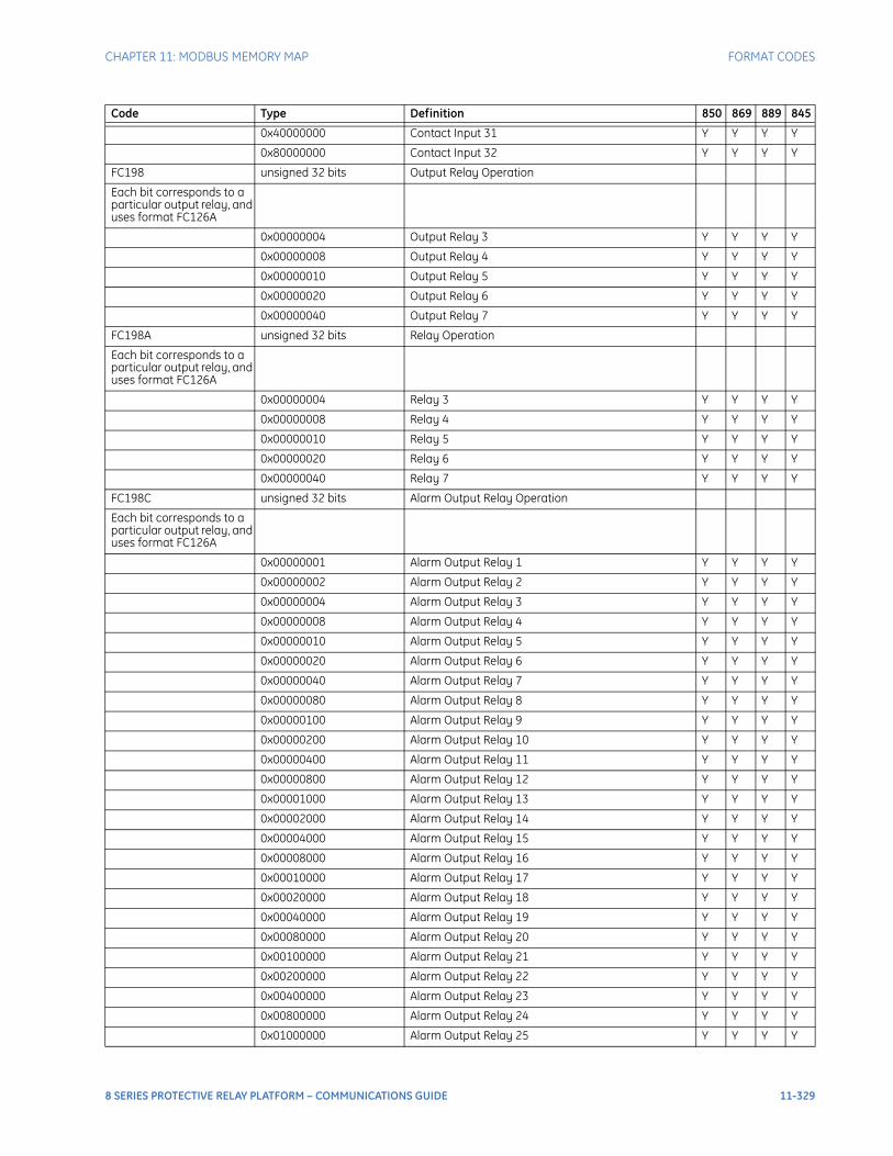
CHAPTER 11: MODBUS MEMORY MAP FORMAT CODES
0x40000000 Contact Input 31 Y Y Y Y
0x80000000 Contact Input 32 Y Y Y Y
FC198 unsigned 32 bits Output Relay Operation
Each bit corresponds to a particular output relay, and uses format FC126A
0x00000004 Output Relay 3 Y Y Y Y
0x00000008 Output Relay 4 Y Y Y Y
0x00000010 Output Relay 5 Y Y Y Y
0x00000020 Output Relay 6 Y Y Y Y
0x00000040 Output Relay 7 Y Y Y Y
FC198A unsigned 32 bits Relay Operation
Each bit corresponds to a particular output relay, and uses format FC126A
0x00000004 Relay 3 Y Y Y Y
0x00000008 Relay 4 Y Y Y Y
0x00000010 Relay 5 Y Y Y Y
0x00000020 Relay 6 Y Y Y Y
0x00000040 Relay 7 Y Y Y Y
FC198C unsigned 32 bits Alarm Output Relay Operation
Each bit corresponds to a particular output relay, and uses format FC126A
0x00000001 Alarm Output Relay 1 Y Y Y Y
0x00000002 Alarm Output Relay 2 Y Y Y Y
0x00000004 Alarm Output Relay 3 Y Y Y Y
0x00000008 Alarm Output Relay 4 Y Y Y Y
0x00000010 Alarm Output Relay 5 Y Y Y Y
0x00000020 Alarm Output Relay 6 Y Y Y Y
0x00000040 Alarm Output Relay 7 Y Y Y Y
0x00000080 Alarm Output Relay 8 Y Y Y Y
0x00000100 Alarm Output Relay 9 Y Y Y Y
0x00000200 Alarm Output Relay 10 Y Y Y Y
0x00000400 Alarm Output Relay 11 Y Y Y Y
0x00000800 Alarm Output Relay 12 Y Y Y Y
0x00001000 Alarm Output Relay 13 Y Y Y Y
0x00002000 Alarm Output Relay 14 Y Y Y Y
0x00004000 Alarm Output Relay 15 Y Y Y Y
0x00008000 Alarm Output Relay 16 Y Y Y Y
0x00010000 Alarm Output Relay 17 Y Y Y Y
0x00020000 Alarm Output Relay 18 Y Y Y Y
0x00040000 Alarm Output Relay 19 Y Y Y Y
0x00080000 Alarm Output Relay 20 Y Y Y Y
0x00100000 Alarm Output Relay 21 Y Y Y Y
0x00200000 Alarm Output Relay 22 Y Y Y Y
0x00400000 Alarm Output Relay 23 Y Y Y Y
0x00800000 Alarm Output Relay 24 Y Y Y Y
0x01000000 Alarm Output Relay 25 Y Y Y Y
Code Type Definition 850 869 889 845
8 SERIES PROTECTIVE RELAY PLATFORM – COMMUNICATIONS GUIDE 11-329
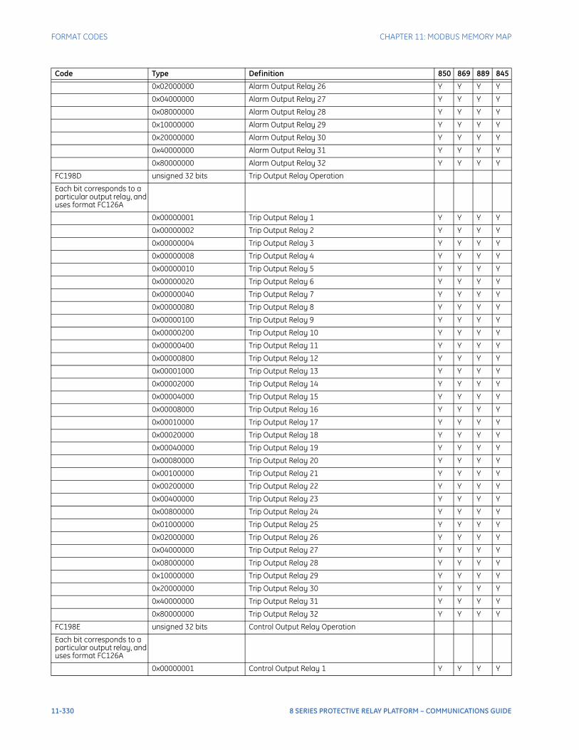
FORMAT CODES CHAPTER 11: MODBUS MEMORY MAP
0x02000000 Alarm Output Relay 26 Y Y Y Y
0x04000000 Alarm Output Relay 27 Y Y Y Y
0x08000000 Alarm Output Relay 28 Y Y Y Y
0x10000000 Alarm Output Relay 29 Y Y Y Y
0x20000000 Alarm Output Relay 30 Y Y Y Y
0x40000000 Alarm Output Relay 31 Y Y Y Y
0x80000000 Alarm Output Relay 32 Y Y Y Y
FC198D unsigned 32 bits Trip Output Relay Operation
Each bit corresponds to a particular output relay, and uses format FC126A
0x00000001 Trip Output Relay 1 Y Y Y Y
0x00000002 Trip Output Relay 2 Y Y Y Y
0x00000004 Trip Output Relay 3 Y Y Y Y
0x00000008 Trip Output Relay 4 Y Y Y Y
0x00000010 Trip Output Relay 5 Y Y Y Y
0x00000020 Trip Output Relay 6 Y Y Y Y
0x00000040 Trip Output Relay 7 Y Y Y Y
0x00000080 Trip Output Relay 8 Y Y Y Y
0x00000100 Trip Output Relay 9 Y Y Y Y
0x00000200 Trip Output Relay 10 Y Y Y Y
0x00000400 Trip Output Relay 11 Y Y Y Y
0x00000800 Trip Output Relay 12 Y Y Y Y
0x00001000 Trip Output Relay 13 Y Y Y Y
0x00002000 Trip Output Relay 14 Y Y Y Y
0x00004000 Trip Output Relay 15 Y Y Y Y
0x00008000 Trip Output Relay 16 Y Y Y Y
0x00010000 Trip Output Relay 17 Y Y Y Y
0x00020000 Trip Output Relay 18 Y Y Y Y
0x00040000 Trip Output Relay 19 Y Y Y Y
0x00080000 Trip Output Relay 20 Y Y Y Y
0x00100000 Trip Output Relay 21 Y Y Y Y
0x00200000 Trip Output Relay 22 Y Y Y Y
0x00400000 Trip Output Relay 23 Y Y Y Y
0x00800000 Trip Output Relay 24 Y Y Y Y
0x01000000 Trip Output Relay 25 Y Y Y Y
0x02000000 Trip Output Relay 26 Y Y Y Y
0x04000000 Trip Output Relay 27 Y Y Y Y
0x08000000 Trip Output Relay 28 Y Y Y Y
0x10000000 Trip Output Relay 29 Y Y Y Y
0x20000000 Trip Output Relay 30 Y Y Y Y
0x40000000 Trip Output Relay 31 Y Y Y Y
0x80000000 Trip Output Relay 32 Y Y Y Y
FC198E unsigned 32 bits Control Output Relay Operation
Each bit corresponds to a particular output relay, and uses format FC126A
0x00000001 Control Output Relay 1 Y Y Y Y
Code Type Definition 850 869 889 845
11-330 8 SERIES PROTECTIVE RELAY PLATFORM – COMMUNICATIONS GUIDE
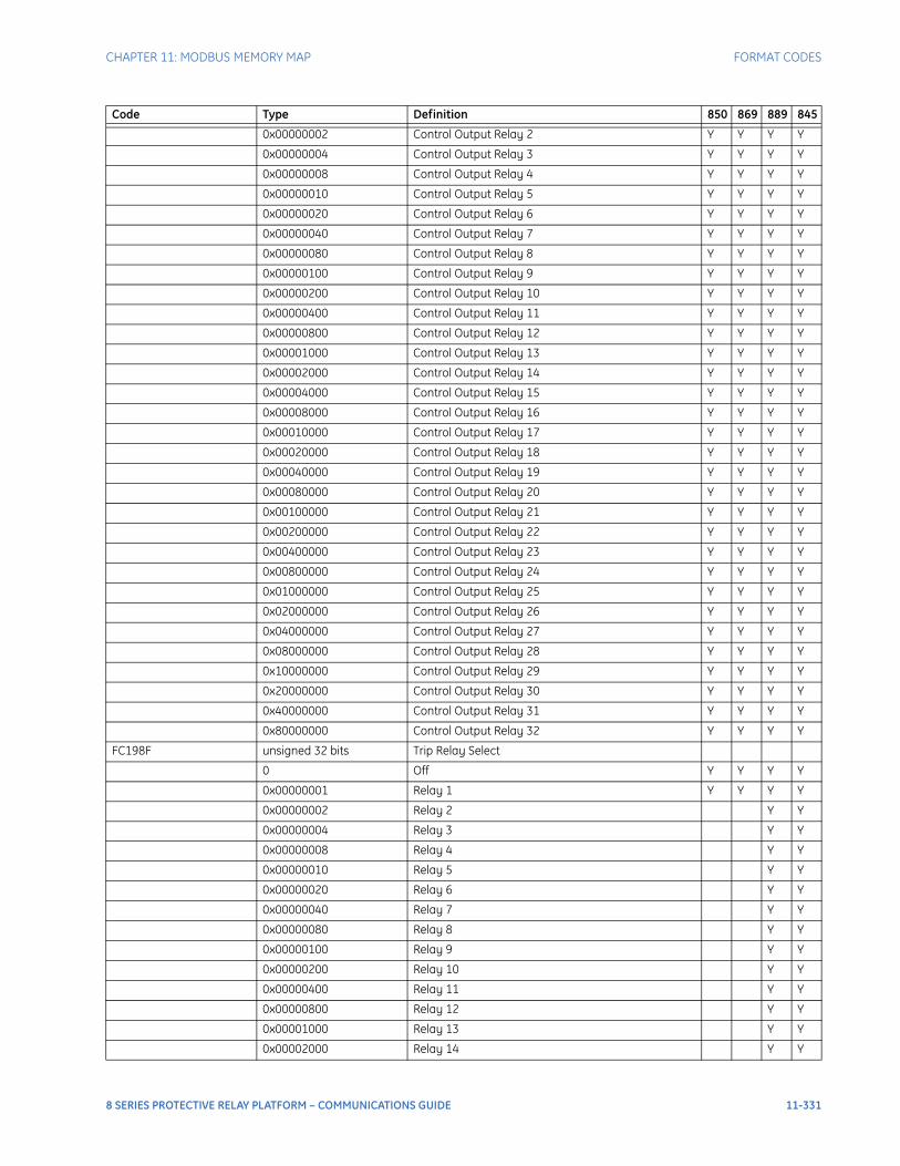
CHAPTER 11: MODBUS MEMORY MAP FORMAT CODES
0x00000002 Control Output Relay 2 Y Y Y Y
0x00000004 Control Output Relay 3 Y Y Y Y
0x00000008 Control Output Relay 4 Y Y Y Y
0x00000010 Control Output Relay 5 Y Y Y Y
0x00000020 Control Output Relay 6 Y Y Y Y
0x00000040 Control Output Relay 7 Y Y Y Y
0x00000080 Control Output Relay 8 Y Y Y Y
0x00000100 Control Output Relay 9 Y Y Y Y
0x00000200 Control Output Relay 10 Y Y Y Y
0x00000400 Control Output Relay 11 Y Y Y Y
0x00000800 Control Output Relay 12 Y Y Y Y
0x00001000 Control Output Relay 13 Y Y Y Y
0x00002000 Control Output Relay 14 Y Y Y Y
0x00004000 Control Output Relay 15 Y Y Y Y
0x00008000 Control Output Relay 16 Y Y Y Y
0x00010000 Control Output Relay 17 Y Y Y Y
0x00020000 Control Output Relay 18 Y Y Y Y
0x00040000 Control Output Relay 19 Y Y Y Y
0x00080000 Control Output Relay 20 Y Y Y Y
0x00100000 Control Output Relay 21 Y Y Y Y
0x00200000 Control Output Relay 22 Y Y Y Y
0x00400000 Control Output Relay 23 Y Y Y Y
0x00800000 Control Output Relay 24 Y Y Y Y
0x01000000 Control Output Relay 25 Y Y Y Y
0x02000000 Control Output Relay 26 Y Y Y Y
0x04000000 Control Output Relay 27 Y Y Y Y
0x08000000 Control Output Relay 28 Y Y Y Y
0x10000000 Control Output Relay 29 Y Y Y Y
0x20000000 Control Output Relay 30 Y Y Y Y
0x40000000 Control Output Relay 31 Y Y Y Y
0x80000000 Control Output Relay 32 Y Y Y Y
FC198F unsigned 32 bits Trip Relay Select
0 Off Y Y Y Y
0x00000001 Relay 1 Y Y Y Y
0x00000002 Relay 2 Y Y
0x00000004 Relay 3 Y Y
0x00000008 Relay 4 Y Y
0x00000010 Relay 5 Y Y
0x00000020 Relay 6 Y Y
0x00000040 Relay 7 Y Y
0x00000080 Relay 8 Y Y
0x00000100 Relay 9 Y Y
0x00000200 Relay 10 Y Y
0x00000400 Relay 11 Y Y
0x00000800 Relay 12 Y Y
0x00001000 Relay 13 Y Y
0x00002000 Relay 14 Y Y
Code Type Definition 850 869 889 845
8 SERIES PROTECTIVE RELAY PLATFORM – COMMUNICATIONS GUIDE 11-331
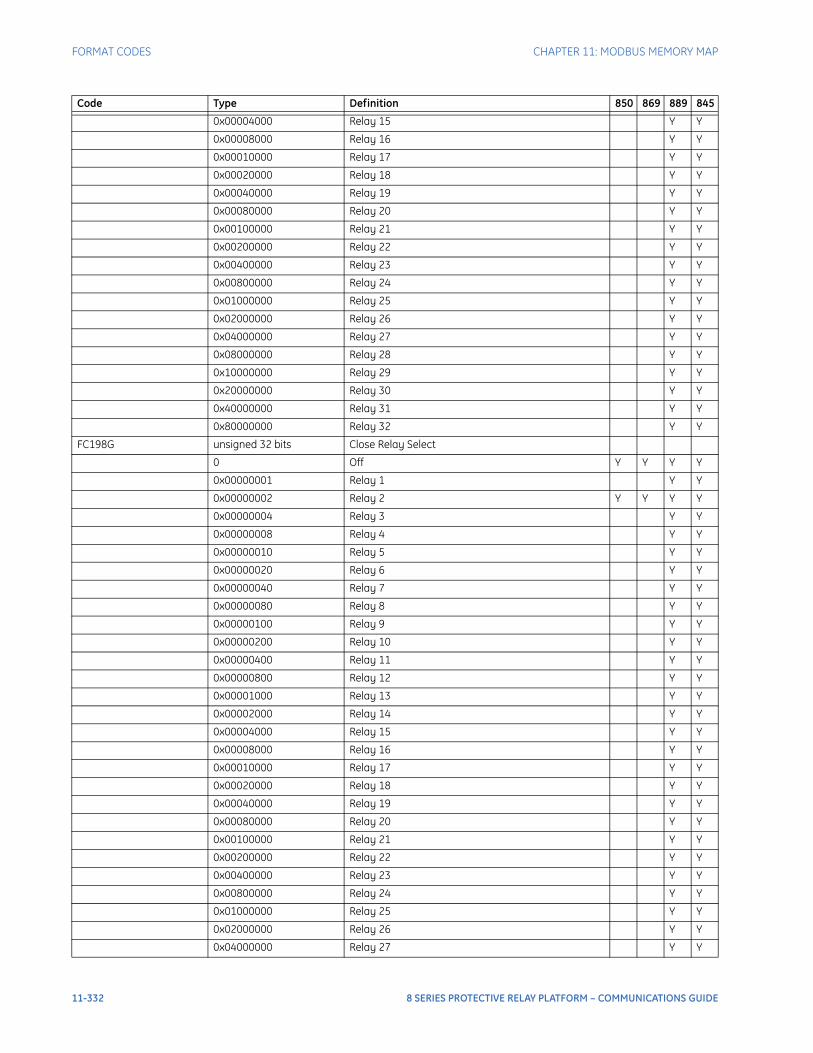
FORMAT CODES CHAPTER 11: MODBUS MEMORY MAP
0x00004000 Relay 15 Y Y
0x00008000 Relay 16 Y Y
0x00010000 Relay 17 Y Y
0x00020000 Relay 18 Y Y
0x00040000 Relay 19 Y Y
0x00080000 Relay 20 Y Y
0x00100000 Relay 21 Y Y
0x00200000 Relay 22 Y Y
0x00400000 Relay 23 Y Y
0x00800000 Relay 24 Y Y
0x01000000 Relay 25 Y Y
0x02000000 Relay 26 Y Y
0x04000000 Relay 27 Y Y
0x08000000 Relay 28 Y Y
0x10000000 Relay 29 Y Y
0x20000000 Relay 30 Y Y
0x40000000 Relay 31 Y Y
0x80000000 Relay 32 Y Y
FC198G unsigned 32 bits Close Relay Select
0 Off Y Y Y Y
0x00000001 Relay 1 Y Y
0x00000002 Relay 2 Y Y Y Y
0x00000004 Relay 3 Y Y
0x00000008 Relay 4 Y Y
0x00000010 Relay 5 Y Y
0x00000020 Relay 6 Y Y
0x00000040 Relay 7 Y Y
0x00000080 Relay 8 Y Y
0x00000100 Relay 9 Y Y
0x00000200 Relay 10 Y Y
0x00000400 Relay 11 Y Y
0x00000800 Relay 12 Y Y
0x00001000 Relay 13 Y Y
0x00002000 Relay 14 Y Y
0x00004000 Relay 15 Y Y
0x00008000 Relay 16 Y Y
0x00010000 Relay 17 Y Y
0x00020000 Relay 18 Y Y
0x00040000 Relay 19 Y Y
0x00080000 Relay 20 Y Y
0x00100000 Relay 21 Y Y
0x00200000 Relay 22 Y Y
0x00400000 Relay 23 Y Y
0x00800000 Relay 24 Y Y
0x01000000 Relay 25 Y Y
0x02000000 Relay 26 Y Y
0x04000000 Relay 27 Y Y
Code Type Definition 850 869 889 845
11-332 8 SERIES PROTECTIVE RELAY PLATFORM – COMMUNICATIONS GUIDE

CHAPTER 11: MODBUS MEMORY MAP FORMAT CODES
0x08000000 Relay 28 Y Y
0x10000000 Relay 29 Y Y
0x20000000 Relay 30 Y Y
0x40000000 Relay 31 Y Y
0x80000000 Relay 32 Y Y
FC198H unsigned 32 bits Percent Differential Relays
Each bit corresponds to a particular output relay, and uses format FC126A
0x00000001 Output Relay 1 Y Y Y Y
0x00000002 Output Relay 2 Y Y Y Y
0x00000004 Output Relay 3 Y Y Y Y
0x00000008 Output Relay 4 Y Y Y Y
0x00000010 Output Relay 5 Y Y Y Y
0x00000020 Output Relay 6 Y Y Y Y
0x00000040 Output Relay 7 Y Y Y Y
0x00000080 Output Relay 8 Y Y Y Y
0x00000100 Output Relay 9 Y Y Y Y
0x00000200 Output Relay 10 Y Y Y Y
0x00000400 Output Relay 11 Y Y Y Y
0x00000800 Output Relay 12 Y Y Y Y
0x00001000 Output Relay 13 Y Y Y Y
0x00002000 Output Relay 14 Y Y Y Y
0x00004000 Output Relay 15 Y Y Y Y
0x00008000 Output Relay 16 Y Y Y Y
0x00010000 Output Relay 17 Y Y Y Y
0x00020000 Output Relay 18 Y Y Y Y
0x00040000 Output Relay 19 Y Y Y Y
0x00080000 Output Relay 20 Y Y Y Y
0x00100000 Output Relay 21 Y Y Y Y
0x00200000 Output Relay 22 Y Y Y Y
0x00400000 Output Relay 23 Y Y Y Y
0x00800000 Output Relay 24 Y Y Y Y
0x01000000 Output Relay 25 Y Y Y Y
0x02000000 Output Relay 26 Y Y Y Y
0x04000000 Output Relay 27 Y Y Y Y
0x08000000 Output Relay 28 Y Y Y Y
0x10000000 Output Relay 29 Y Y Y Y
0x20000000 Output Relay 30 Y Y Y Y
0x40000000 Output Relay 31 Y Y Y Y
0x80000000 Output Relay 32 Y Y Y Y
FC198I unsigned 32 bits Instantaneous Differential Relays
Each bit corresponds to a particular output relay, and uses format FC126A
0x00000001 Inst Diff Output Relay 1 Y Y Y Y
0x00000002 Inst Diff Output Relay 2 Y Y Y Y
0x00000004 Inst Diff Output Relay 3 Y Y Y Y
Code Type Definition 850 869 889 845
8 SERIES PROTECTIVE RELAY PLATFORM – COMMUNICATIONS GUIDE 11-333
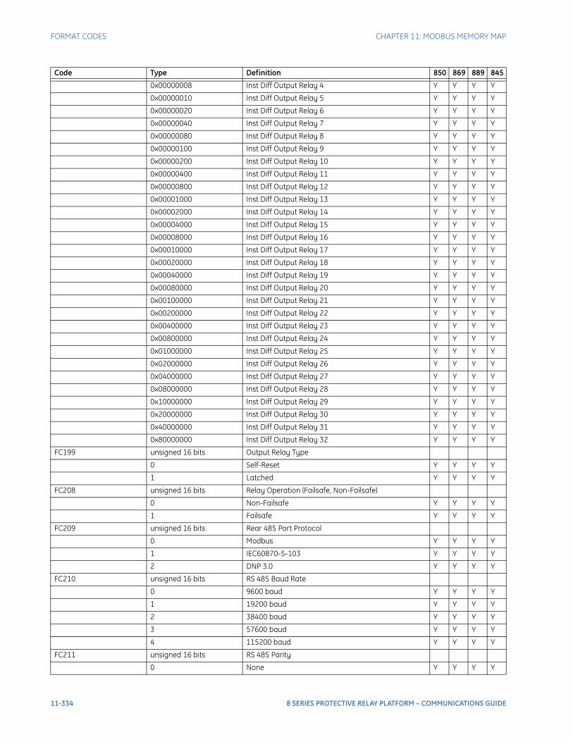
FORMAT CODES CHAPTER 11: MODBUS MEMORY MAP
0x00000008 Inst Diff Output Relay 4 Y Y Y Y
0x00000010 Inst Diff Output Relay 5 Y Y Y Y
0x00000020 Inst Diff Output Relay 6 Y Y Y Y
0x00000040 Inst Diff Output Relay 7 Y Y Y Y
0x00000080 Inst Diff Output Relay 8 Y Y Y Y
0x00000100 Inst Diff Output Relay 9 Y Y Y Y
0x00000200 Inst Diff Output Relay 10 Y Y Y Y
0x00000400 Inst Diff Output Relay 11 Y Y Y Y
0x00000800 Inst Diff Output Relay 12 Y Y Y Y
0x00001000 Inst Diff Output Relay 13 Y Y Y Y
0x00002000 Inst Diff Output Relay 14 Y Y Y Y
0x00004000 Inst Diff Output Relay 15 Y Y Y Y
0x00008000 Inst Diff Output Relay 16 Y Y Y Y
0x00010000 Inst Diff Output Relay 17 Y Y Y Y
0x00020000 Inst Diff Output Relay 18 Y Y Y Y
0x00040000 Inst Diff Output Relay 19 Y Y Y Y
0x00080000 Inst Diff Output Relay 20 Y Y Y Y
0x00100000 Inst Diff Output Relay 21 Y Y Y Y
0x00200000 Inst Diff Output Relay 22 Y Y Y Y
0x00400000 Inst Diff Output Relay 23 Y Y Y Y
0x00800000 Inst Diff Output Relay 24 Y Y Y Y
0x01000000 Inst Diff Output Relay 25 Y Y Y Y
0x02000000 Inst Diff Output Relay 26 Y Y Y Y
0x04000000 Inst Diff Output Relay 27 Y Y Y Y
0x08000000 Inst Diff Output Relay 28 Y Y Y Y
0x10000000 Inst Diff Output Relay 29 Y Y Y Y
0x20000000 Inst Diff Output Relay 30 Y Y Y Y
0x40000000 Inst Diff Output Relay 31 Y Y Y Y
0x80000000 Inst Diff Output Relay 32 Y Y Y Y
FC199 unsigned 16 bits Output Relay Type
0 Self-Reset Y Y Y Y
1 Latched Y Y Y Y
FC208 unsigned 16 bits Relay Operation (Failsafe, Non-Failsafe)
0 Non-Failsafe Y Y Y Y
1 Failsafe Y Y Y Y
FC209 unsigned 16 bits Rear 485 Port Protocol
0 Modbus Y Y Y Y
1 IEC60870-5-103 Y Y Y Y
2 DNP 3.0 Y Y Y Y
FC210 unsigned 16 bits RS 485 Baud Rate
0 9600 baud Y Y Y Y
1 19200 baud Y Y Y Y
2 38400 baud Y Y Y Y
3 57600 baud Y Y Y Y
4 115200 baud Y Y Y Y
FC211 unsigned 16 bits RS 485 Parity
0 None Y Y Y Y
Code Type Definition 850 869 889 845
11-334 8 SERIES PROTECTIVE RELAY PLATFORM – COMMUNICATIONS GUIDE
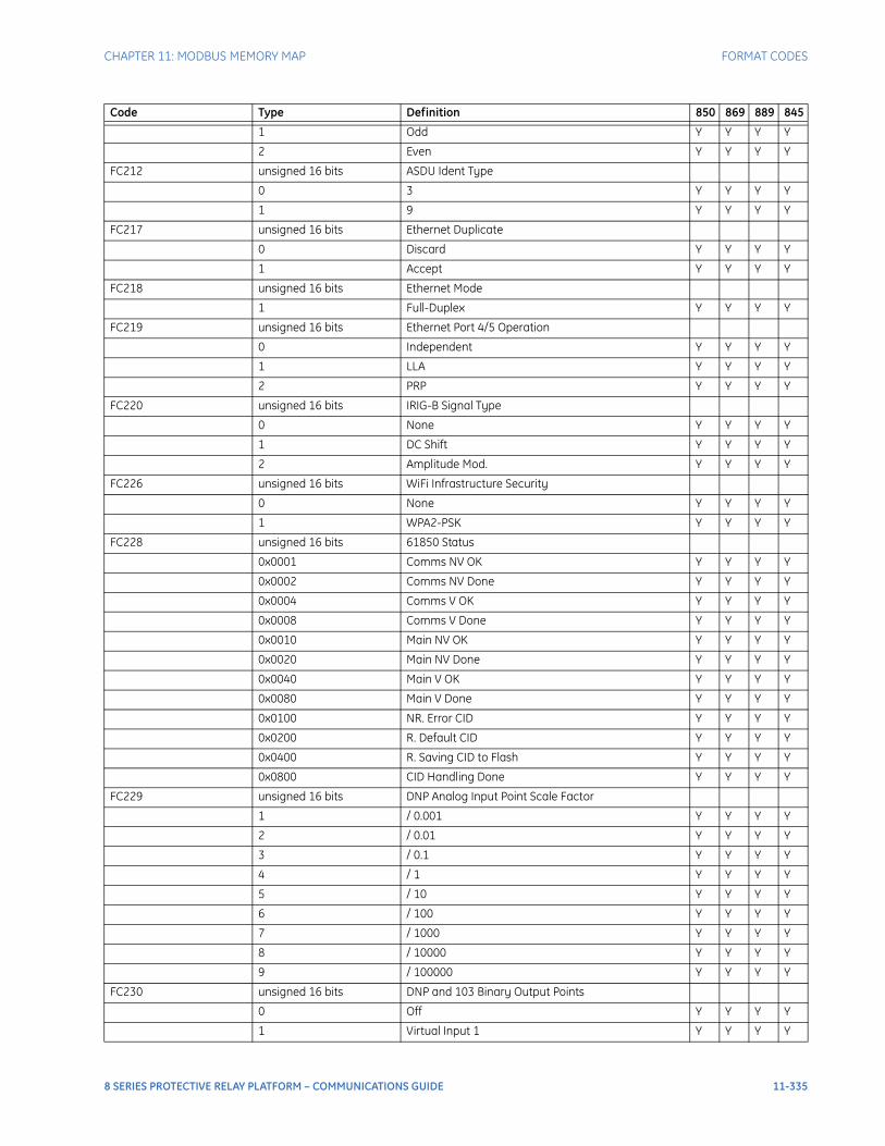
CHAPTER 11: MODBUS MEMORY MAP FORMAT CODES
1 Odd Y Y Y Y
2 Even Y Y Y Y
FC212 unsigned 16 bits ASDU Ident Type
0 3 Y Y Y Y
1 9 Y Y Y Y
FC217 unsigned 16 bits Ethernet Duplicate
0 Discard Y Y Y Y
1 Accept Y Y Y Y
FC218 unsigned 16 bits Ethernet Mode
1 Full-Duplex Y Y Y Y
FC219 unsigned 16 bits Ethernet Port 4/5 Operation
0 Independent Y Y Y Y
1 LLA Y Y Y Y
2 PRP Y Y Y Y
FC220 unsigned 16 bits IRIG-B Signal Type
0 None Y Y Y Y
1 DC Shift Y Y Y Y
2 Amplitude Mod. Y Y Y Y
FC226 unsigned 16 bits WiFi Infrastructure Security
0 None Y Y Y Y
1 WPA2-PSK Y Y Y Y
FC228 unsigned 16 bits 61850 Status
0x0001 Comms NV OK Y Y Y Y
0x0002 Comms NV Done Y Y Y Y
0x0004 Comms V OK Y Y Y Y
0x0008 Comms V Done Y Y Y Y
0x0010 Main NV OK Y Y Y Y
0x0020 Main NV Done Y Y Y Y
0x0040 Main V OK Y Y Y Y
0x0080 Main V Done Y Y Y Y
0x0100 NR. Error CID Y Y Y Y
0x0200 R. Default CID Y Y Y Y
0x0400 R. Saving CID to Flash Y Y Y Y
0x0800 CID Handling Done Y Y Y Y
FC229 unsigned 16 bits DNP Analog Input Point Scale Factor
1 / 0.001 Y Y Y Y
2 / 0.01 Y Y Y Y
3 / 0.1 Y Y Y Y
4 / 1 Y Y Y Y
5 / 10 Y Y Y Y
6 / 100 Y Y Y Y
7 / 1000 Y Y Y Y
8 / 10000 Y Y Y Y
9 / 100000 Y Y Y Y
FC230 unsigned 16 bits DNP and 103 Binary Output Points
0 Off Y Y Y Y
1 Virtual Input 1 Y Y Y Y
Code Type Definition 850 869 889 845
8 SERIES PROTECTIVE RELAY PLATFORM – COMMUNICATIONS GUIDE 11-335
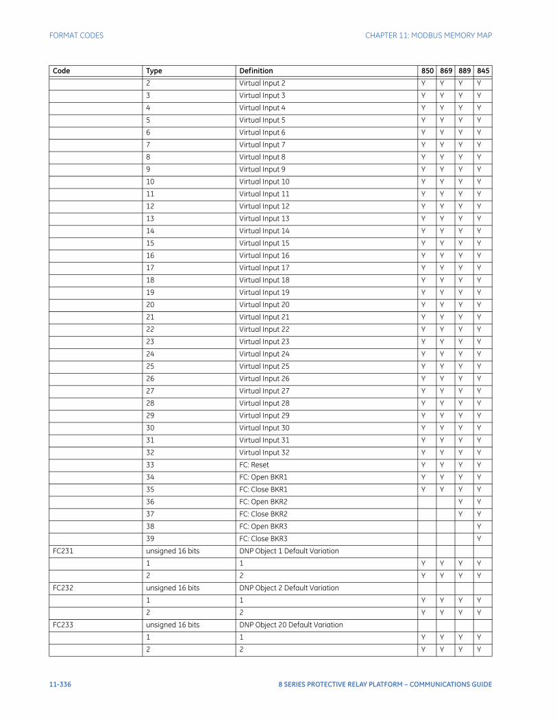
FORMAT CODES CHAPTER 11: MODBUS MEMORY MAP
2 Virtual Input 2 Y Y Y Y
3 Virtual Input 3 Y Y Y Y
4 Virtual Input 4 Y Y Y Y
5 Virtual Input 5 Y Y Y Y
6 Virtual Input 6 Y Y Y Y
7 Virtual Input 7 Y Y Y Y
8 Virtual Input 8 Y Y Y Y
9 Virtual Input 9 Y Y Y Y
10 Virtual Input 10 Y Y Y Y
11 Virtual Input 11 Y Y Y Y
12 Virtual Input 12 Y Y Y Y
13 Virtual Input 13 Y Y Y Y
14 Virtual Input 14 Y Y Y Y
15 Virtual Input 15 Y Y Y Y
16 Virtual Input 16 Y Y Y Y
17 Virtual Input 17 Y Y Y Y
18 Virtual Input 18 Y Y Y Y
19 Virtual Input 19 Y Y Y Y
20 Virtual Input 20 Y Y Y Y
21 Virtual Input 21 Y Y Y Y
22 Virtual Input 22 Y Y Y Y
23 Virtual Input 23 Y Y Y Y
24 Virtual Input 24 Y Y Y Y
25 Virtual Input 25 Y Y Y Y
26 Virtual Input 26 Y Y Y Y
27 Virtual Input 27 Y Y Y Y
28 Virtual Input 28 Y Y Y Y
29 Virtual Input 29 Y Y Y Y
30 Virtual Input 30 Y Y Y Y
31 Virtual Input 31 Y Y Y Y
32 Virtual Input 32 Y Y Y Y
33 FC: Reset Y Y Y Y
34 FC: Open BKR1 Y Y Y Y
35 FC: Close BKR1 Y Y Y Y
36 FC: Open BKR2 Y Y
37 FC: Close BKR2 Y Y
38 FC: Open BKR3 Y
39 FC: Close BKR3 Y
FC231 unsigned 16 bits DNP Object 1 Default Variation
1 1 Y Y Y Y
2 2 Y Y Y Y
FC232 unsigned 16 bits DNP Object 2 Default Variation
1 1 Y Y Y Y
2 2 Y Y Y Y
FC233 unsigned 16 bits DNP Object 20 Default Variation
1 1 Y Y Y Y
2 2 Y Y Y Y
Code Type Definition 850 869 889 845
11-336 8 SERIES PROTECTIVE RELAY PLATFORM – COMMUNICATIONS GUIDE
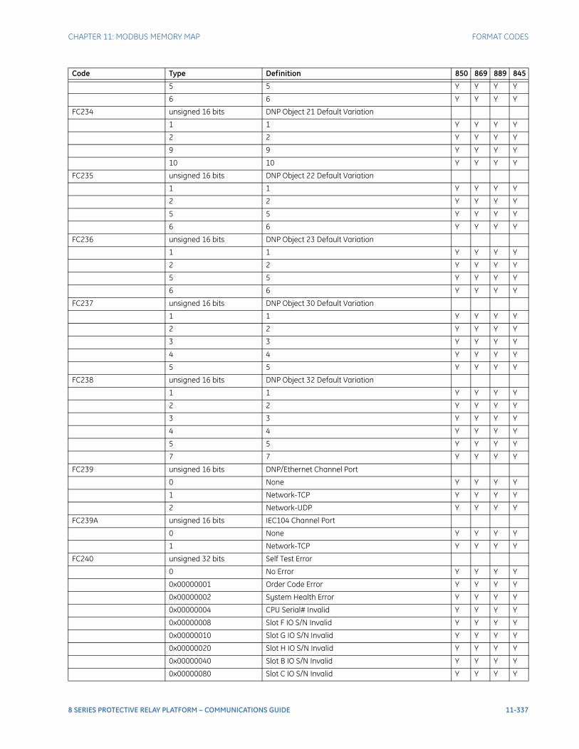
CHAPTER 11: MODBUS MEMORY MAP FORMAT CODES
5 5 Y Y Y Y
6 6 Y Y Y Y
FC234 unsigned 16 bits DNP Object 21 Default Variation
1 1 Y Y Y Y
2 2 Y Y Y Y
9 9 Y Y Y Y
10 10 Y Y Y Y
FC235 unsigned 16 bits DNP Object 22 Default Variation
1 1 Y Y Y Y
2 2 Y Y Y Y
5 5 Y Y Y Y
6 6 Y Y Y Y
FC236 unsigned 16 bits DNP Object 23 Default Variation
1 1 Y Y Y Y
2 2 Y Y Y Y
5 5 Y Y Y Y
6 6 Y Y Y Y
FC237 unsigned 16 bits DNP Object 30 Default Variation
1 1 Y Y Y Y
2 2 Y Y Y Y
3 3 Y Y Y Y
4 4 Y Y Y Y
5 5 Y Y Y Y
FC238 unsigned 16 bits DNP Object 32 Default Variation
1 1 Y Y Y Y
2 2 Y Y Y Y
3 3 Y Y Y Y
4 4 Y Y Y Y
5 5 Y Y Y Y
7 7 Y Y Y Y
FC239 unsigned 16 bits DNP/Ethernet Channel Port
0 None Y Y Y Y
1 Network-TCP Y Y Y Y
2 Network-UDP Y Y Y Y
FC239A unsigned 16 bits IEC104 Channel Port
0 None Y Y Y Y
1 Network-TCP Y Y Y Y
FC240 unsigned 32 bits Self Test Error
0 No Error Y Y Y Y
0x00000001 Order Code Error Y Y Y Y
0x00000002 System Health Error Y Y Y Y
0x00000004 CPU Serial# Invalid Y Y Y Y
0x00000008 Slot F IO S/N Invalid Y Y Y Y
0x00000010 Slot G IO S/N Invalid Y Y Y Y
0x00000020 Slot H IO S/N Invalid Y Y Y Y
0x00000040 Slot B IO S/N Invalid Y Y Y Y
0x00000080 Slot C IO S/N Invalid Y Y Y Y
Code Type Definition 850 869 889 845
8 SERIES PROTECTIVE RELAY PLATFORM – COMMUNICATIONS GUIDE 11-337
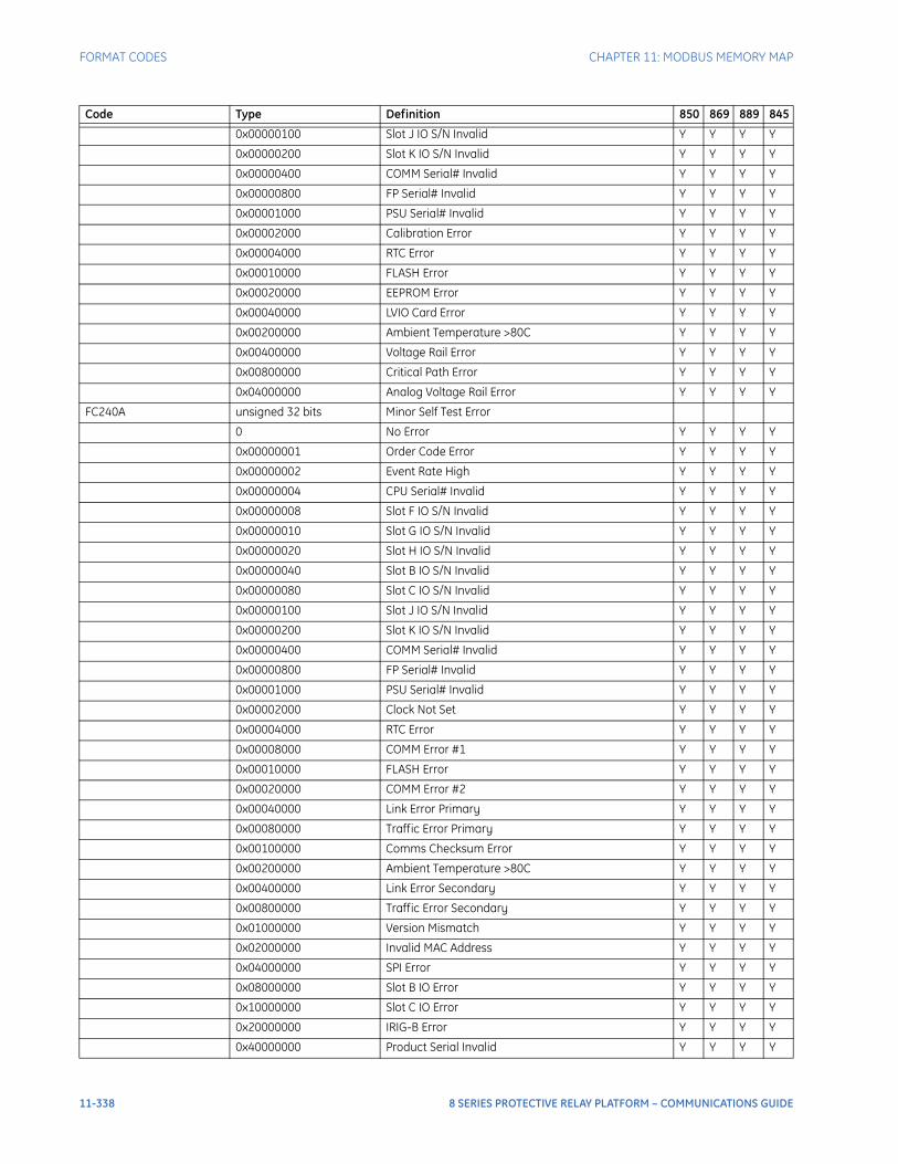
FORMAT CODES CHAPTER 11: MODBUS MEMORY MAP
0x00000100 Slot J IO S/N Invalid Y Y Y Y
0x00000200 Slot K IO S/N Invalid Y Y Y Y
0x00000400 COMM Serial# Invalid Y Y Y Y
0x00000800 FP Serial# Invalid Y Y Y Y
0x00001000 PSU Serial# Invalid Y Y Y Y
0x00002000 Calibration Error Y Y Y Y
0x00004000 RTC Error Y Y Y Y
0x00010000 FLASH Error Y Y Y Y
0x00020000 EEPROM Error Y Y Y Y
0x00040000 LVIO Card Error Y Y Y Y
0x00200000 Ambient Temperature >80C Y Y Y Y
0x00400000 Voltage Rail Error Y Y Y Y
0x00800000 Critical Path Error Y Y Y Y
0x04000000 Analog Voltage Rail Error Y Y Y Y
FC240A unsigned 32 bits Minor Self Test Error
0 No Error Y Y Y Y
0x00000001 Order Code Error Y Y Y Y
0x00000002 Event Rate High Y Y Y Y
0x00000004 CPU Serial# Invalid Y Y Y Y
0x00000008 Slot F IO S/N Invalid Y Y Y Y
0x00000010 Slot G IO S/N Invalid Y Y Y Y
0x00000020 Slot H IO S/N Invalid Y Y Y Y
0x00000040 Slot B IO S/N Invalid Y Y Y Y
0x00000080 Slot C IO S/N Invalid Y Y Y Y
0x00000100 Slot J IO S/N Invalid Y Y Y Y
0x00000200 Slot K IO S/N Invalid Y Y Y Y
0x00000400 COMM Serial# Invalid Y Y Y Y
0x00000800 FP Serial# Invalid Y Y Y Y
0x00001000 PSU Serial# Invalid Y Y Y Y
0x00002000 Clock Not Set Y Y Y Y
0x00004000 RTC Error Y Y Y Y
0x00008000 COMM Error #1 Y Y Y Y
0x00010000 FLASH Error Y Y Y Y
0x00020000 COMM Error #2 Y Y Y Y
0x00040000 Link Error Primary Y Y Y Y
0x00080000 Traffic Error Primary Y Y Y Y
0x00100000 Comms Checksum Error Y Y Y Y
0x00200000 Ambient Temperature >80C Y Y Y Y
0x00400000 Link Error Secondary Y Y Y Y
0x00800000 Traffic Error Secondary Y Y Y Y
0x01000000 Version Mismatch Y Y Y Y
0x02000000 Invalid MAC Address Y Y Y Y
0x04000000 SPI Error Y Y Y Y
0x08000000 Slot B IO Error Y Y Y Y
0x10000000 Slot C IO Error Y Y Y Y
0x20000000 IRIG-B Error Y Y Y Y
0x40000000 Product Serial Invalid Y Y Y Y
Code Type Definition 850 869 889 845
11-338 8 SERIES PROTECTIVE RELAY PLATFORM – COMMUNICATIONS GUIDE
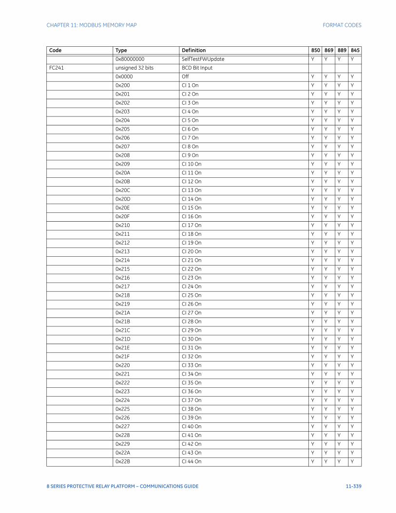
CHAPTER 11: MODBUS MEMORY MAP FORMAT CODES
0x80000000 SelfTestFWUpdate Y Y Y Y
FC241 unsigned 32 bits BCD Bit Input
0x0000 Off Y Y Y Y
0x200 CI 1 On Y Y Y Y
0x201 CI 2 On Y Y Y Y
0x202 CI 3 On Y Y Y Y
0x203 CI 4 On Y Y Y Y
0x204 CI 5 On Y Y Y Y
0x205 CI 6 On Y Y Y Y
0x206 CI 7 On Y Y Y Y
0x207 CI 8 On Y Y Y Y
0x208 CI 9 On Y Y Y Y
0x209 CI 10 On Y Y Y Y
0x20A CI 11 On Y Y Y Y
0x20B CI 12 On Y Y Y Y
0x20C CI 13 On Y Y Y Y
0x20D CI 14 On Y Y Y Y
0x20E CI 15 On Y Y Y Y
0x20F CI 16 On Y Y Y Y
0x210 CI 17 On Y Y Y Y
0x211 CI 18 On Y Y Y Y
0x212 CI 19 On Y Y Y Y
0x213 CI 20 On Y Y Y Y
0x214 CI 21 On Y Y Y Y
0x215 CI 22 On Y Y Y Y
0x216 CI 23 On Y Y Y Y
0x217 CI 24 On Y Y Y Y
0x218 CI 25 On Y Y Y Y
0x219 CI 26 On Y Y Y Y
0x21A CI 27 On Y Y Y Y
0x21B CI 28 On Y Y Y Y
0x21C CI 29 On Y Y Y Y
0x21D CI 30 On Y Y Y Y
0x21E CI 31 On Y Y Y Y
0x21F CI 32 On Y Y Y Y
0x220 CI 33 On Y Y Y Y
0x221 CI 34 On Y Y Y Y
0x222 CI 35 On Y Y Y Y
0x223 CI 36 On Y Y Y Y
0x224 CI 37 On Y Y Y Y
0x225 CI 38 On Y Y Y Y
0x226 CI 39 On Y Y Y Y
0x227 CI 40 On Y Y Y Y
0x228 CI 41 On Y Y Y Y
0x229 CI 42 On Y Y Y Y
0x22A CI 43 On Y Y Y Y
0x22B CI 44 On Y Y Y Y
Code Type Definition 850 869 889 845
8 SERIES PROTECTIVE RELAY PLATFORM – COMMUNICATIONS GUIDE 11-339
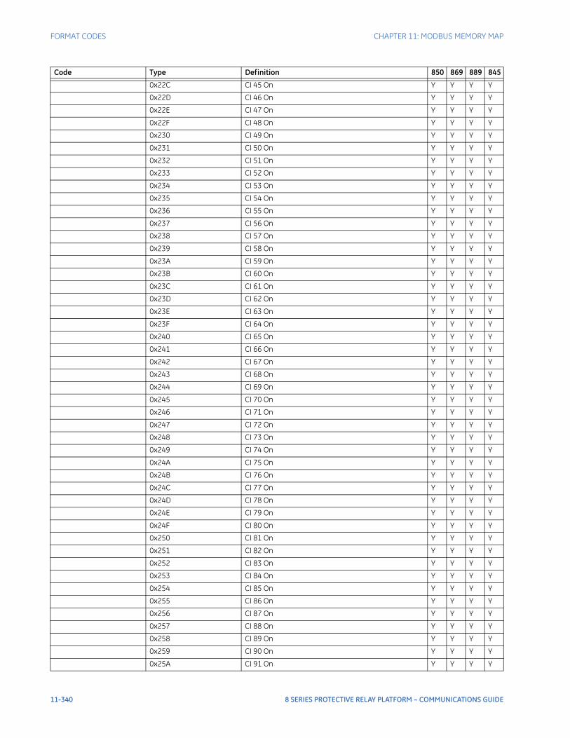
FORMAT CODES CHAPTER 11: MODBUS MEMORY MAP
0x22C CI 45 On Y Y Y Y
0x22D CI 46 On Y Y Y Y
0x22E CI 47 On Y Y Y Y
0x22F CI 48 On Y Y Y Y
0x230 CI 49 On Y Y Y Y
0x231 CI 50 On Y Y Y Y
0x232 CI 51 On Y Y Y Y
0x233 CI 52 On Y Y Y Y
0x234 CI 53 On Y Y Y Y
0x235 CI 54 On Y Y Y Y
0x236 CI 55 On Y Y Y Y
0x237 CI 56 On Y Y Y Y
0x238 CI 57 On Y Y Y Y
0x239 CI 58 On Y Y Y Y
0x23A CI 59 On Y Y Y Y
0x23B CI 60 On Y Y Y Y
0x23C CI 61 On Y Y Y Y
0x23D CI 62 On Y Y Y Y
0x23E CI 63 On Y Y Y Y
0x23F CI 64 On Y Y Y Y
0x240 CI 65 On Y Y Y Y
0x241 CI 66 On Y Y Y Y
0x242 CI 67 On Y Y Y Y
0x243 CI 68 On Y Y Y Y
0x244 CI 69 On Y Y Y Y
0x245 CI 70 On Y Y Y Y
0x246 CI 71 On Y Y Y Y
0x247 CI 72 On Y Y Y Y
0x248 CI 73 On Y Y Y Y
0x249 CI 74 On Y Y Y Y
0x24A CI 75 On Y Y Y Y
0x24B CI 76 On Y Y Y Y
0x24C CI 77 On Y Y Y Y
0x24D CI 78 On Y Y Y Y
0x24E CI 79 On Y Y Y Y
0x24F CI 80 On Y Y Y Y
0x250 CI 81 On Y Y Y Y
0x251 CI 82 On Y Y Y Y
0x252 CI 83 On Y Y Y Y
0x253 CI 84 On Y Y Y Y
0x254 CI 85 On Y Y Y Y
0x255 CI 86 On Y Y Y Y
0x256 CI 87 On Y Y Y Y
0x257 CI 88 On Y Y Y Y
0x258 CI 89 On Y Y Y Y
0x259 CI 90 On Y Y Y Y
0x25A CI 91 On Y Y Y Y
Code Type Definition 850 869 889 845
11-340 8 SERIES PROTECTIVE RELAY PLATFORM – COMMUNICATIONS GUIDE
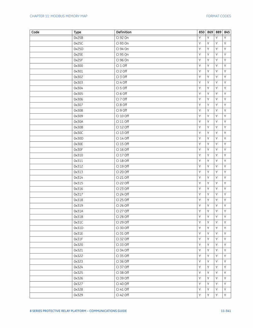
CHAPTER 11: MODBUS MEMORY MAP FORMAT CODES
0x25B CI 92 On Y Y Y Y
0x25C CI 93 On Y Y Y Y
0x25D CI 94 On Y Y Y Y
0x25E CI 95 On Y Y Y Y
0x25F CI 96 On Y Y Y Y
0x300 CI 1 Off Y Y Y Y
0x301 CI 2 Off Y Y Y Y
0x302 CI 3 Off Y Y Y Y
0x303 CI 4 Off Y Y Y Y
0x304 CI 5 Off Y Y Y Y
0x305 CI 6 Off Y Y Y Y
0x306 CI 7 Off Y Y Y Y
0x307 CI 8 Off Y Y Y Y
0x308 CI 9 Off Y Y Y Y
0x309 CI 10 Off Y Y Y Y
0x30A CI 11 Off Y Y Y Y
0x30B CI 12 Off Y Y Y Y
0x30C CI 13 Off Y Y Y Y
0x30D CI 14 Off Y Y Y Y
0x30E CI 15 Off Y Y Y Y
0x30F CI 16 Off Y Y Y Y
0x310 CI 17 Off Y Y Y Y
0x311 CI 18 Off Y Y Y Y
0x312 CI 19 Off Y Y Y Y
0x313 CI 20 Off Y Y Y Y
0x314 CI 21 Off Y Y Y Y
0x315 CI 22 Off Y Y Y Y
0x316 CI 23 Off Y Y Y Y
0x317 CI 24 Off Y Y Y Y
0x318 CI 25 Off Y Y Y Y
0x319 CI 26 Off Y Y Y Y
0x31A CI 27 Off Y Y Y Y
0x31B CI 28 Off Y Y Y Y
0x31C CI 29 Off Y Y Y Y
0x31D CI 30 Off Y Y Y Y
0x31E CI 31 Off Y Y Y Y
0x31F CI 32 Off Y Y Y Y
0x320 CI 33 Off Y Y Y Y
0x321 CI 34 Off Y Y Y Y
0x322 CI 35 Off Y Y Y Y
0x323 CI 36 Off Y Y Y Y
0x324 CI 37 Off Y Y Y Y
0x325 CI 38 Off Y Y Y Y
0x326 CI 39 Off Y Y Y Y
0x327 CI 40 Off Y Y Y Y
0x328 CI 41 Off Y Y Y Y
0x329 CI 42 Off Y Y Y Y
Code Type Definition 850 869 889 845
8 SERIES PROTECTIVE RELAY PLATFORM – COMMUNICATIONS GUIDE 11-341
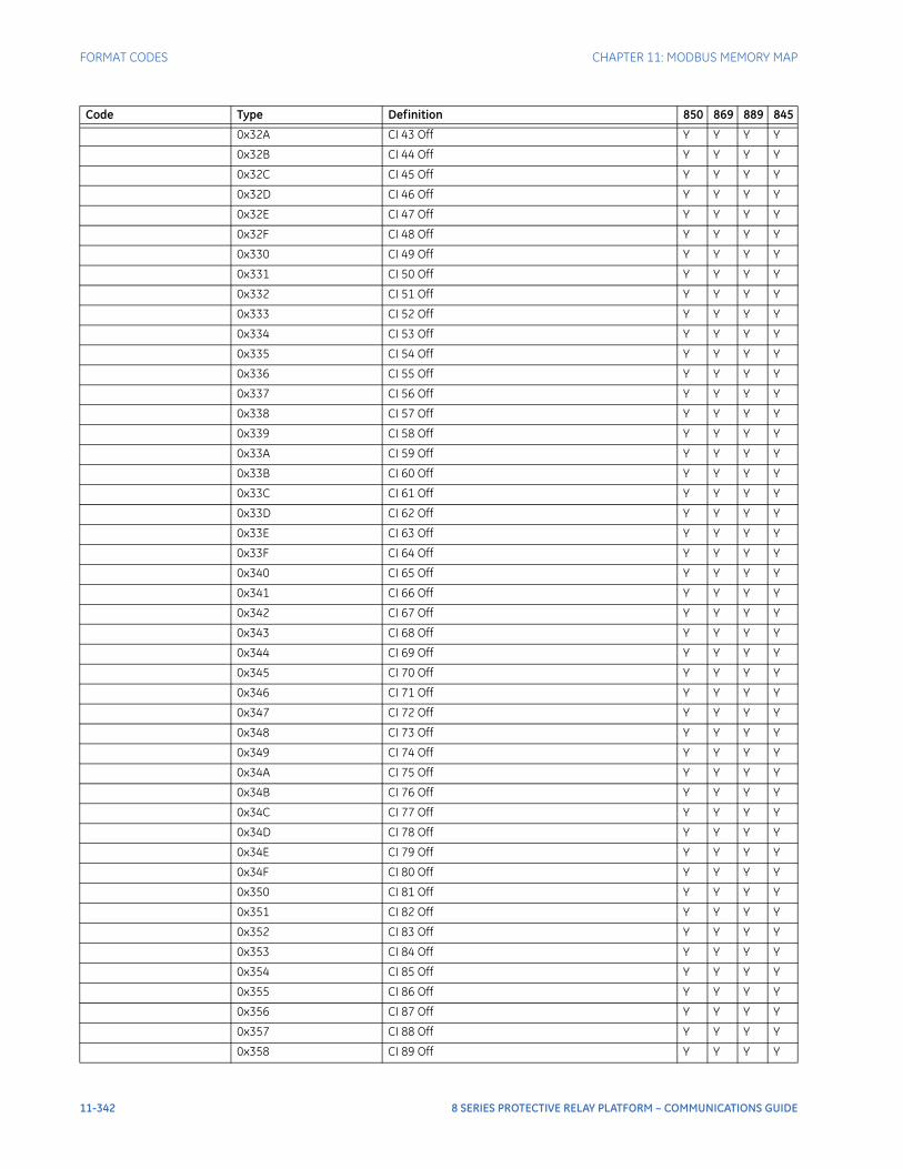
FORMAT CODES CHAPTER 11: MODBUS MEMORY MAP
0x32A CI 43 Off Y Y Y Y
0x32B CI 44 Off Y Y Y Y
0x32C CI 45 Off Y Y Y Y
0x32D CI 46 Off Y Y Y Y
0x32E CI 47 Off Y Y Y Y
0x32F CI 48 Off Y Y Y Y
0x330 CI 49 Off Y Y Y Y
0x331 CI 50 Off Y Y Y Y
0x332 CI 51 Off Y Y Y Y
0x333 CI 52 Off Y Y Y Y
0x334 CI 53 Off Y Y Y Y
0x335 CI 54 Off Y Y Y Y
0x336 CI 55 Off Y Y Y Y
0x337 CI 56 Off Y Y Y Y
0x338 CI 57 Off Y Y Y Y
0x339 CI 58 Off Y Y Y Y
0x33A CI 59 Off Y Y Y Y
0x33B CI 60 Off Y Y Y Y
0x33C CI 61 Off Y Y Y Y
0x33D CI 62 Off Y Y Y Y
0x33E CI 63 Off Y Y Y Y
0x33F CI 64 Off Y Y Y Y
0x340 CI 65 Off Y Y Y Y
0x341 CI 66 Off Y Y Y Y
0x342 CI 67 Off Y Y Y Y
0x343 CI 68 Off Y Y Y Y
0x344 CI 69 Off Y Y Y Y
0x345 CI 70 Off Y Y Y Y
0x346 CI 71 Off Y Y Y Y
0x347 CI 72 Off Y Y Y Y
0x348 CI 73 Off Y Y Y Y
0x349 CI 74 Off Y Y Y Y
0x34A CI 75 Off Y Y Y Y
0x34B CI 76 Off Y Y Y Y
0x34C CI 77 Off Y Y Y Y
0x34D CI 78 Off Y Y Y Y
0x34E CI 79 Off Y Y Y Y
0x34F CI 80 Off Y Y Y Y
0x350 CI 81 Off Y Y Y Y
0x351 CI 82 Off Y Y Y Y
0x352 CI 83 Off Y Y Y Y
0x353 CI 84 Off Y Y Y Y
0x354 CI 85 Off Y Y Y Y
0x355 CI 86 Off Y Y Y Y
0x356 CI 87 Off Y Y Y Y
0x357 CI 88 Off Y Y Y Y
0x358 CI 89 Off Y Y Y Y
Code Type Definition 850 869 889 845
11-342 8 SERIES PROTECTIVE RELAY PLATFORM – COMMUNICATIONS GUIDE
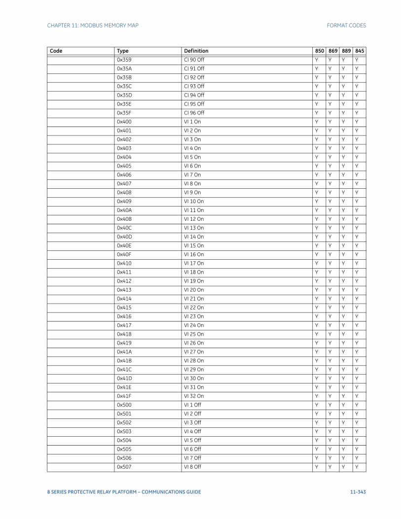
CHAPTER 11: MODBUS MEMORY MAP FORMAT CODES
0x359 CI 90 Off Y Y Y Y
0x35A CI 91 Off Y Y Y Y
0x35B CI 92 Off Y Y Y Y
0x35C CI 93 Off Y Y Y Y
0x35D CI 94 Off Y Y Y Y
0x35E CI 95 Off Y Y Y Y
0x35F CI 96 Off Y Y Y Y
0x400 VI 1 On Y Y Y Y
0x401 VI 2 On Y Y Y Y
0x402 VI 3 On Y Y Y Y
0x403 VI 4 On Y Y Y Y
0x404 VI 5 On Y Y Y Y
0x405 VI 6 On Y Y Y Y
0x406 VI 7 On Y Y Y Y
0x407 VI 8 On Y Y Y Y
0x408 VI 9 On Y Y Y Y
0x409 VI 10 On Y Y Y Y
0x40A VI 11 On Y Y Y Y
0x40B VI 12 On Y Y Y Y
0x40C VI 13 On Y Y Y Y
0x40D VI 14 On Y Y Y Y
0x40E VI 15 On Y Y Y Y
0x40F VI 16 On Y Y Y Y
0x410 VI 17 On Y Y Y Y
0x411 VI 18 On Y Y Y Y
0x412 VI 19 On Y Y Y Y
0x413 VI 20 On Y Y Y Y
0x414 VI 21 On Y Y Y Y
0x415 VI 22 On Y Y Y Y
0x416 VI 23 On Y Y Y Y
0x417 VI 24 On Y Y Y Y
0x418 VI 25 On Y Y Y Y
0x419 VI 26 On Y Y Y Y
0x41A VI 27 On Y Y Y Y
0x41B VI 28 On Y Y Y Y
0x41C VI 29 On Y Y Y Y
0x41D VI 30 On Y Y Y Y
0x41E VI 31 On Y Y Y Y
0x41F VI 32 On Y Y Y Y
0x500 VI 1 Off Y Y Y Y
0x501 VI 2 Off Y Y Y Y
0x502 VI 3 Off Y Y Y Y
0x503 VI 4 Off Y Y Y Y
0x504 VI 5 Off Y Y Y Y
0x505 VI 6 Off Y Y Y Y
0x506 VI 7 Off Y Y Y Y
0x507 VI 8 Off Y Y Y Y
Code Type Definition 850 869 889 845
8 SERIES PROTECTIVE RELAY PLATFORM – COMMUNICATIONS GUIDE 11-343
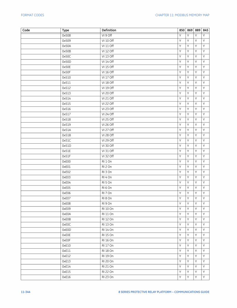
FORMAT CODES CHAPTER 11: MODBUS MEMORY MAP
0x508 VI 9 Off Y Y Y Y
0x509 VI 10 Off Y Y Y Y
0x50A VI 11 Off Y Y Y Y
0x50B VI 12 Off Y Y Y Y
0x50C VI 13 Off Y Y Y Y
0x50D VI 14 Off Y Y Y Y
0x50E VI 15 Off Y Y Y Y
0x50F VI 16 Off Y Y Y Y
0x510 VI 17 Off Y Y Y Y
0x511 VI 18 Off Y Y Y Y
0x512 VI 19 Off Y Y Y Y
0x513 VI 20 Off Y Y Y Y
0x514 VI 21 Off Y Y Y Y
0x515 VI 22 Off Y Y Y Y
0x516 VI 23 Off Y Y Y Y
0x517 VI 24 Off Y Y Y Y
0x518 VI 25 Off Y Y Y Y
0x519 VI 26 Off Y Y Y Y
0x51A VI 27 Off Y Y Y Y
0x51B VI 28 Off Y Y Y Y
0x51C VI 29 Off Y Y Y Y
0x51D VI 30 Off Y Y Y Y
0x51E VI 31 Off Y Y Y Y
0x51F VI 32 Off Y Y Y Y
0xE00 RI 1 On Y Y Y Y
0xE01 RI 2 On Y Y Y Y
0xE02 RI 3 On Y Y Y Y
0xE03 RI 4 On Y Y Y Y
0xE04 RI 5 On Y Y Y Y
0xE05 RI 6 On Y Y Y Y
0xE06 RI 7 On Y Y Y Y
0xE07 RI 8 On Y Y Y Y
0xE08 RI 9 On Y Y Y Y
0xE09 RI 10 On Y Y Y Y
0xE0A RI 11 On Y Y Y Y
0xE0B RI 12 On Y Y Y Y
0xE0C RI 13 On Y Y Y Y
0xE0D RI 14 On Y Y Y Y
0xE0E RI 15 On Y Y Y Y
0xE0F RI 16 On Y Y Y Y
0xE10 RI 17 On Y Y Y Y
0xE11 RI 18 On Y Y Y Y
0xE12 RI 19 On Y Y Y Y
0xE13 RI 20 On Y Y Y Y
0xE14 RI 21 On Y Y Y Y
0xE15 RI 22 On Y Y Y Y
0xE16 RI 23 On Y Y Y Y
Code Type Definition 850 869 889 845
11-344 8 SERIES PROTECTIVE RELAY PLATFORM – COMMUNICATIONS GUIDE
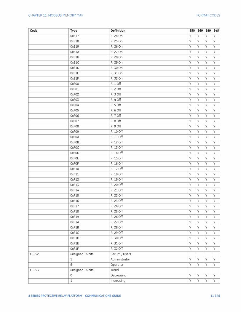
CHAPTER 11: MODBUS MEMORY MAP FORMAT CODES
0xE17 RI 24 On Y Y Y Y
0xE18 RI 25 On Y Y Y Y
0xE19 RI 26 On Y Y Y Y
0xE1A RI 27 On Y Y Y Y
0xE1B RI 28 On Y Y Y Y
0xE1C RI 29 On Y Y Y Y
0xE1D RI 30 On Y Y Y Y
0xE1E RI 31 On Y Y Y Y
0xE1F RI 32 On Y Y Y Y
0xF00 RI 1 Off Y Y Y Y
0xF01 RI 2 Off Y Y Y Y
0xF02 RI 3 Off Y Y Y Y
0xF03 RI 4 Off Y Y Y Y
0xF04 RI 5 Off Y Y Y Y
0xF05 RI 6 Off Y Y Y Y
0xF06 RI 7 Off Y Y Y Y
0xF07 RI 8 Off Y Y Y Y
0xF08 RI 9 Off Y Y Y Y
0xF09 RI 10 Off Y Y Y Y
0xF0A RI 11 Off Y Y Y Y
0xF0B RI 12 Off Y Y Y Y
0xF0C RI 13 Off Y Y Y Y
0xF0D RI 14 Off Y Y Y Y
0xF0E RI 15 Off Y Y Y Y
0xF0F RI 16 Off Y Y Y Y
0xF10 RI 17 Off Y Y Y Y
0xF11 RI 18 Off Y Y Y Y
0xF12 RI 19 Off Y Y Y Y
0xF13 RI 20 Off Y Y Y Y
0xF14 RI 21 Off Y Y Y Y
0xF15 RI 22 Off Y Y Y Y
0xF16 RI 23 Off Y Y Y Y
0xF17 RI 24 Off Y Y Y Y
0xF18 RI 25 Off Y Y Y Y
0xF19 RI 26 Off Y Y Y Y
0xF1A RI 27 Off Y Y Y Y
0xF1B RI 28 Off Y Y Y Y
0xF1C RI 29 Off Y Y Y Y
0xF1D RI 30 Off Y Y Y Y
0xF1E RI 31 Off Y Y Y Y
0xF1F RI 32 Off Y Y Y Y
FC252 unsigned 16 bits Security Users
1 Administrator Y Y Y Y
6 Operator Y Y Y Y
FC253 unsigned 16 bits Trend
0 Decreasing Y Y Y Y
1 Increasing Y Y Y Y
Code Type Definition 850 869 889 845
8 SERIES PROTECTIVE RELAY PLATFORM – COMMUNICATIONS GUIDE 11-345
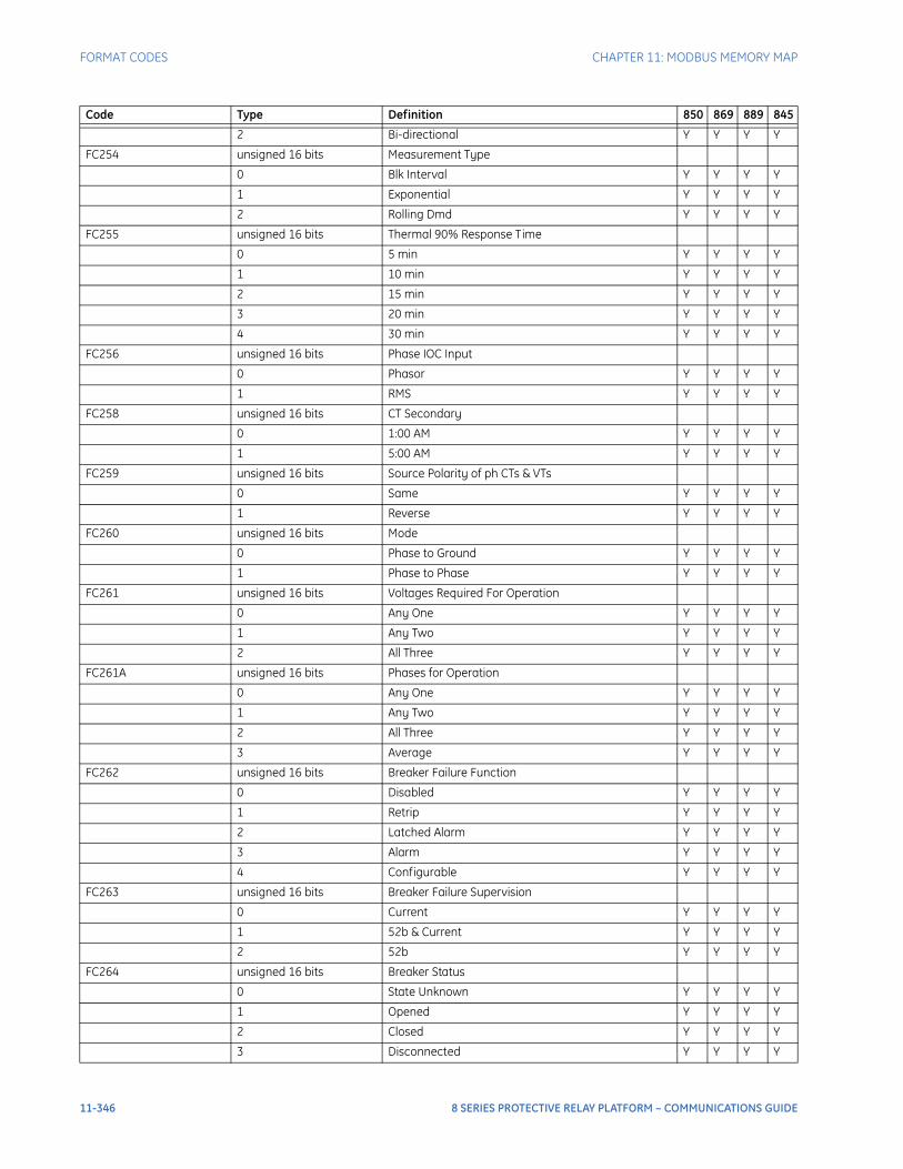
FORMAT CODES CHAPTER 11: MODBUS MEMORY MAP
2 Bi-directional Y Y Y Y
FC254 unsigned 16 bits Measurement Type
0 Blk Interval Y Y Y Y
1 Exponential Y Y Y Y
2 Rolling Dmd Y Y Y Y
FC255 unsigned 16 bits Thermal 90% Response Time
0 5 min Y Y Y Y
1 10 min Y Y Y Y
2 15 min Y Y Y Y
3 20 min Y Y Y Y
4 30 min Y Y Y Y
FC256 unsigned 16 bits Phase IOC Input
0 Phasor Y Y Y Y
1 RMS Y Y Y Y
FC258 unsigned 16 bits CT Secondary
0 1:00 AM Y Y Y Y
1 5:00 AM Y Y Y Y
FC259 unsigned 16 bits Source Polarity of ph CTs & VTs
0 Same Y Y Y Y
1 Reverse Y Y Y Y
FC260 unsigned 16 bits Mode
0 Phase to Ground Y Y Y Y
1 Phase to Phase Y Y Y Y
FC261 unsigned 16 bits Voltages Required For Operation
0 Any One Y Y Y Y
1 Any Two Y Y Y Y
2 All Three Y Y Y Y
FC261A unsigned 16 bits Phases for Operation
0 Any One Y Y Y Y
1 Any Two Y Y Y Y
2 All Three Y Y Y Y
3 Average Y Y Y Y
FC262 unsigned 16 bits Breaker Failure Function
0 Disabled Y Y Y Y
1 Retrip Y Y Y Y
2 Latched Alarm Y Y Y Y
3 Alarm Y Y Y Y
4 Configurable Y Y Y Y
FC263 unsigned 16 bits Breaker Failure Supervision
0 Current Y Y Y Y
1 52b & Current Y Y Y Y
2 52b Y Y Y Y
FC264 unsigned 16 bits Breaker Status
0 State Unknown Y Y Y Y
1 Opened Y Y Y Y
2 Closed Y Y Y Y
3 Disconnected Y Y Y Y
Code Type Definition 850 869 889 845
11-346 8 SERIES PROTECTIVE RELAY PLATFORM – COMMUNICATIONS GUIDE
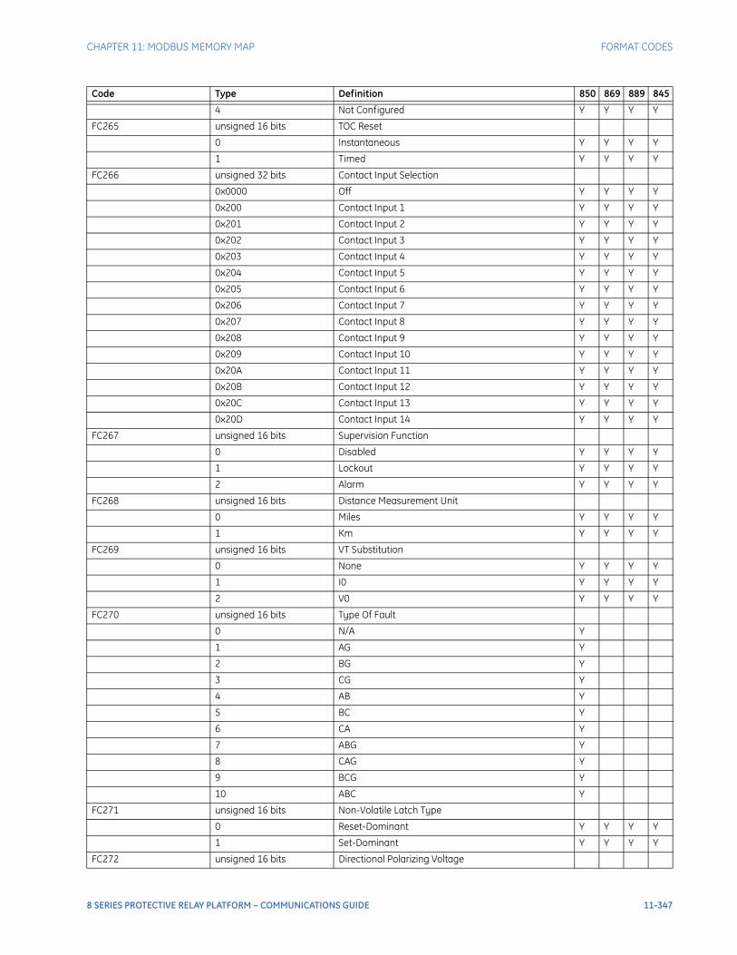
CHAPTER 11: MODBUS MEMORY MAP FORMAT CODES
4 Not Configured Y Y Y Y
FC265 unsigned 16 bits TOC Reset
0 Instantaneous Y Y Y Y
1 Timed Y Y Y Y
FC266 unsigned 32 bits Contact Input Selection
0x0000 Off Y Y Y Y
0x200 Contact Input 1 Y Y Y Y
0x201 Contact Input 2 Y Y Y Y
0x202 Contact Input 3 Y Y Y Y
0x203 Contact Input 4 Y Y Y Y
0x204 Contact Input 5 Y Y Y Y
0x205 Contact Input 6 Y Y Y Y
0x206 Contact Input 7 Y Y Y Y
0x207 Contact Input 8 Y Y Y Y
0x208 Contact Input 9 Y Y Y Y
0x209 Contact Input 10 Y Y Y Y
0x20A Contact Input 11 Y Y Y Y
0x20B Contact Input 12 Y Y Y Y
0x20C Contact Input 13 Y Y Y Y
0x20D Contact Input 14 Y Y Y Y
FC267 unsigned 16 bits Supervision Function
0 Disabled Y Y Y Y
1 Lockout Y Y Y Y
2 Alarm Y Y Y Y
FC268 unsigned 16 bits Distance Measurement Unit
0 Miles Y Y Y Y
1 Km Y Y Y Y
FC269 unsigned 16 bits VT Substitution
0 None Y Y Y Y
1 I0 Y Y Y Y
2 V0 Y Y Y Y
FC270 unsigned 16 bits Type Of Fault
0 N/A Y
1 AG Y
2 BG Y
3 CG Y
4 AB Y
5 BC Y
6 CA Y
7 ABG Y
8 CAG Y
9 BCG Y
10 ABC Y
FC271 unsigned 16 bits Non-Volatile Latch Type
0 Reset-Dominant Y Y Y Y
1 Set-Dominant Y Y Y Y
FC272 unsigned 16 bits Directional Polarizing Voltage
Code Type Definition 850 869 889 845
8 SERIES PROTECTIVE RELAY PLATFORM – COMMUNICATIONS GUIDE 11-347
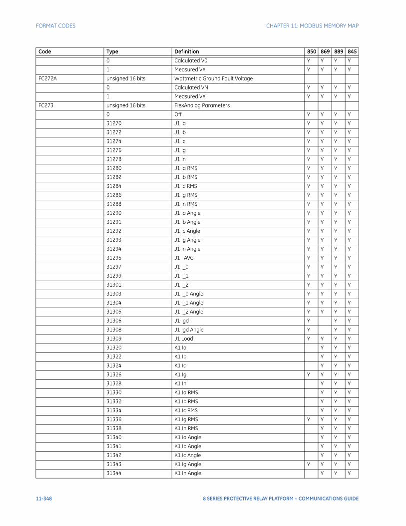
FORMAT CODES CHAPTER 11: MODBUS MEMORY MAP
0 Calculated V0 Y Y Y Y
1 Measured VX Y Y Y Y
FC272A unsigned 16 bits Wattmetric Ground Fault Voltage
0 Calculated VN Y Y Y Y
1 Measured VX Y Y Y Y
FC273 unsigned 16 bits FlexAnalog Parameters
0 Off Y Y Y Y
31270 J1 Ia Y Y Y Y
31272 J1 Ib Y Y Y Y
31274 J1 Ic Y Y Y Y
31276 J1 Ig Y Y Y Y
31278 J1 In Y Y Y Y
31280 J1 Ia RMS Y Y Y Y
31282 J1 Ib RMS Y Y Y Y
31284 J1 Ic RMS Y Y Y Y
31286 J1 Ig RMS Y Y Y Y
31288 J1 In RMS Y Y Y Y
31290 J1 Ia Angle Y Y Y Y
31291 J1 Ib Angle Y Y Y Y
31292 J1 Ic Angle Y Y Y Y
31293 J1 Ig Angle Y Y Y Y
31294 J1 In Angle Y Y Y Y
31295 J1 I AVG Y Y Y Y
31297 J1 I_0 Y Y Y Y
31299 J1 I_1 Y Y Y Y
31301 J1 I_2 Y Y Y Y
31303 J1 I_0 Angle Y Y Y Y
31304 J1 I_1 Angle Y Y Y Y
31305 J1 I_2 Angle Y Y Y Y
31306 J1 Igd Y Y Y
31308 J1 Igd Angle Y Y Y
31309 J1 Load Y Y Y Y
31320 K1 Ia Y Y Y
31322 K1 Ib Y Y Y
31324 K1 Ic Y Y Y
31326 K1 Ig Y Y Y Y
31328 K1 In Y Y Y
31330 K1 Ia RMS Y Y Y
31332 K1 Ib RMS Y Y Y
31334 K1 Ic RMS Y Y Y
31336 K1 Ig RMS Y Y Y Y
31338 K1 In RMS Y Y Y
31340 K1 Ia Angle Y Y Y
31341 K1 Ib Angle Y Y Y
31342 K1 Ic Angle Y Y Y
31343 K1 Ig Angle Y Y Y Y
31344 K1 In Angle Y Y Y
Code Type Definition 850 869 889 845
11-348 8 SERIES PROTECTIVE RELAY PLATFORM – COMMUNICATIONS GUIDE
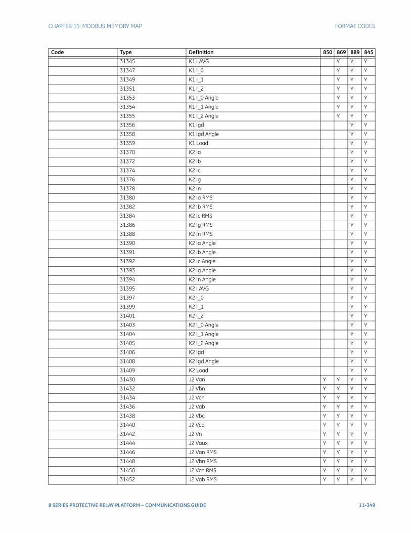
CHAPTER 11: MODBUS MEMORY MAP FORMAT CODES
31345 K1 I AVG Y Y Y
31347 K1 I_0 Y Y Y
31349 K1 I_1 Y Y Y
31351 K1 I_2 Y Y Y
31353 K1 I_0 Angle Y Y Y
31354 K1 I_1 Angle Y Y Y
31355 K1 I_2 Angle Y Y Y
31356 K1 Igd Y Y
31358 K1 Igd Angle Y Y
31359 K1 Load Y Y
31370 K2 Ia Y Y
31372 K2 Ib Y Y
31374 K2 Ic Y Y
31376 K2 Ig Y Y
31378 K2 In Y Y
31380 K2 Ia RMS Y Y
31382 K2 Ib RMS Y Y
31384 K2 Ic RMS Y Y
31386 K2 Ig RMS Y Y
31388 K2 In RMS Y Y
31390 K2 Ia Angle Y Y
31391 K2 Ib Angle Y Y
31392 K2 Ic Angle Y Y
31393 K2 Ig Angle Y Y
31394 K2 In Angle Y Y
31395 K2 I AVG Y Y
31397 K2 I_0 Y Y
31399 K2 I_1 Y Y
31401 K2 I_2 Y Y
31403 K2 I_0 Angle Y Y
31404 K2 I_1 Angle Y Y
31405 K2 I_2 Angle Y Y
31406 K2 Igd Y Y
31408 K2 Igd Angle Y Y
31409 K2 Load Y Y
31430 J2 Van Y Y Y Y
31432 J2 Vbn Y Y Y Y
31434 J2 Vcn Y Y Y Y
31436 J2 Vab Y Y Y Y
31438 J2 Vbc Y Y Y Y
31440 J2 Vca Y Y Y Y
31442 J2 Vn Y Y Y Y
31444 J2 Vaux Y Y Y Y
31446 J2 Van RMS Y Y Y Y
31448 J2 Vbn RMS Y Y Y Y
31450 J2 Vcn RMS Y Y Y Y
31452 J2 Vab RMS Y Y Y Y
Code Type Definition 850 869 889 845
8 SERIES PROTECTIVE RELAY PLATFORM – COMMUNICATIONS GUIDE 11-349
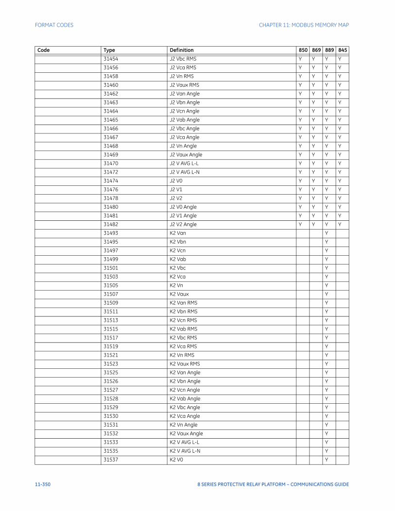
FORMAT CODES CHAPTER 11: MODBUS MEMORY MAP
31454 J2 Vbc RMS Y Y Y Y
31456 J2 Vca RMS Y Y Y Y
31458 J2 Vn RMS Y Y Y Y
31460 J2 Vaux RMS Y Y Y Y
31462 J2 Van Angle Y Y Y Y
31463 J2 Vbn Angle Y Y Y Y
31464 J2 Vcn Angle Y Y Y Y
31465 J2 Vab Angle Y Y Y Y
31466 J2 Vbc Angle Y Y Y Y
31467 J2 Vca Angle Y Y Y Y
31468 J2 Vn Angle Y Y Y Y
31469 J2 Vaux Angle Y Y Y Y
31470 J2 V AVG L-L Y Y Y Y
31472 J2 V AVG L-N Y Y Y Y
31474 J2 V0 Y Y Y Y
31476 J2 V1 Y Y Y Y
31478 J2 V2 Y Y Y Y
31480 J2 V0 Angle Y Y Y Y
31481 J2 V1 Angle Y Y Y Y
31482 J2 V2 Angle Y Y Y Y
31493 K2 Van Y
31495 K2 Vbn Y
31497 K2 Vcn Y
31499 K2 Vab Y
31501 K2 Vbc Y
31503 K2 Vca Y
31505 K2 Vn Y
31507 K2 Vaux Y
31509 K2 Van RMS Y
31511 K2 Vbn RMS Y
31513 K2 Vcn RMS Y
31515 K2 Vab RMS Y
31517 K2 Vbc RMS Y
31519 K2 Vca RMS Y
31521 K2 Vn RMS Y
31523 K2 Vaux RMS Y
31525 K2 Van Angle Y
31526 K2 Vbn Angle Y
31527 K2 Vcn Angle Y
31528 K2 Vab Angle Y
31529 K2 Vbc Angle Y
31530 K2 Vca Angle Y
31531 K2 Vn Angle Y
31532 K2 Vaux Angle Y
31533 K2 V AVG L-L Y
31535 K2 V AVG L-N Y
31537 K2 V0 Y
Code Type Definition 850 869 889 845
11-350 8 SERIES PROTECTIVE RELAY PLATFORM – COMMUNICATIONS GUIDE
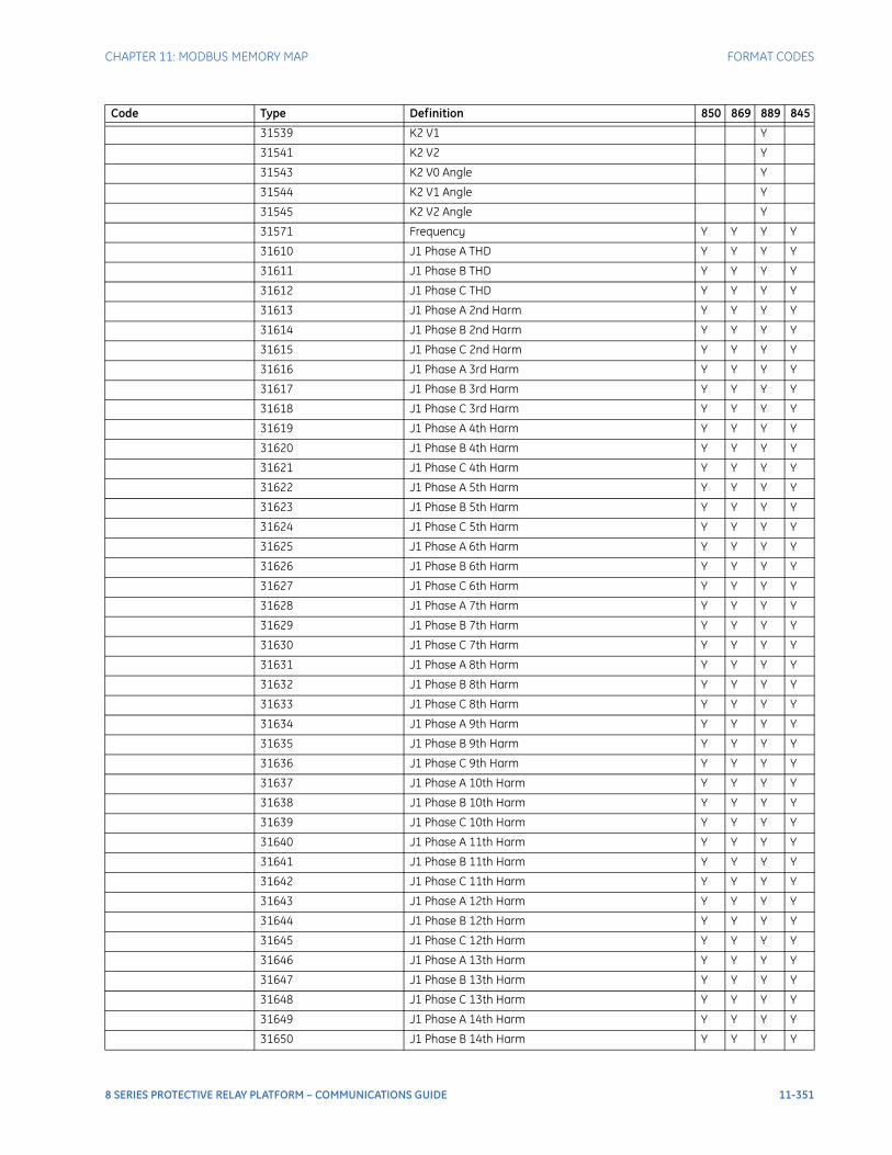
CHAPTER 11: MODBUS MEMORY MAP FORMAT CODES
31539 K2 V1 Y
31541 K2 V2 Y
31543 K2 V0 Angle Y
31544 K2 V1 Angle Y
31545 K2 V2 Angle Y
31571 Frequency Y Y Y Y
31610 J1 Phase A THD Y Y Y Y
31611 J1 Phase B THD Y Y Y Y
31612 J1 Phase C THD Y Y Y Y
31613 J1 Phase A 2nd Harm Y Y Y Y
31614 J1 Phase B 2nd Harm Y Y Y Y
31615 J1 Phase C 2nd Harm Y Y Y Y
31616 J1 Phase A 3rd Harm Y Y Y Y
31617 J1 Phase B 3rd Harm Y Y Y Y
31618 J1 Phase C 3rd Harm Y Y Y Y
31619 J1 Phase A 4th Harm Y Y Y Y
31620 J1 Phase B 4th Harm Y Y Y Y
31621 J1 Phase C 4th Harm Y Y Y Y
31622 J1 Phase A 5th Harm Y Y Y Y
31623 J1 Phase B 5th Harm Y Y Y Y
31624 J1 Phase C 5th Harm Y Y Y Y
31625 J1 Phase A 6th Harm Y Y Y Y
31626 J1 Phase B 6th Harm Y Y Y Y
31627 J1 Phase C 6th Harm Y Y Y Y
31628 J1 Phase A 7th Harm Y Y Y Y
31629 J1 Phase B 7th Harm Y Y Y Y
31630 J1 Phase C 7th Harm Y Y Y Y
31631 J1 Phase A 8th Harm Y Y Y Y
31632 J1 Phase B 8th Harm Y Y Y Y
31633 J1 Phase C 8th Harm Y Y Y Y
31634 J1 Phase A 9th Harm Y Y Y Y
31635 J1 Phase B 9th Harm Y Y Y Y
31636 J1 Phase C 9th Harm Y Y Y Y
31637 J1 Phase A 10th Harm Y Y Y Y
31638 J1 Phase B 10th Harm Y Y Y Y
31639 J1 Phase C 10th Harm Y Y Y Y
31640 J1 Phase A 11th Harm Y Y Y Y
31641 J1 Phase B 11th Harm Y Y Y Y
31642 J1 Phase C 11th Harm Y Y Y Y
31643 J1 Phase A 12th Harm Y Y Y Y
31644 J1 Phase B 12th Harm Y Y Y Y
31645 J1 Phase C 12th Harm Y Y Y Y
31646 J1 Phase A 13th Harm Y Y Y Y
31647 J1 Phase B 13th Harm Y Y Y Y
31648 J1 Phase C 13th Harm Y Y Y Y
31649 J1 Phase A 14th Harm Y Y Y Y
31650 J1 Phase B 14th Harm Y Y Y Y
Code Type Definition 850 869 889 845
8 SERIES PROTECTIVE RELAY PLATFORM – COMMUNICATIONS GUIDE 11-351
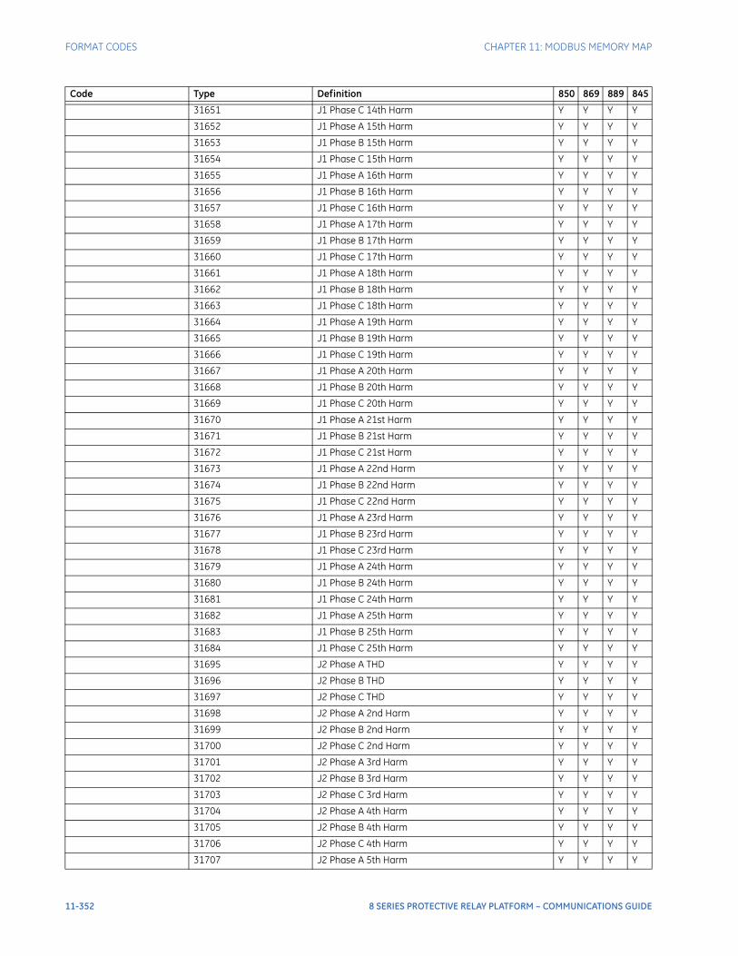
FORMAT CODES CHAPTER 11: MODBUS MEMORY MAP
31651 J1 Phase C 14th Harm Y Y Y Y
31652 J1 Phase A 15th Harm Y Y Y Y
31653 J1 Phase B 15th Harm Y Y Y Y
31654 J1 Phase C 15th Harm Y Y Y Y
31655 J1 Phase A 16th Harm Y Y Y Y
31656 J1 Phase B 16th Harm Y Y Y Y
31657 J1 Phase C 16th Harm Y Y Y Y
31658 J1 Phase A 17th Harm Y Y Y Y
31659 J1 Phase B 17th Harm Y Y Y Y
31660 J1 Phase C 17th Harm Y Y Y Y
31661 J1 Phase A 18th Harm Y Y Y Y
31662 J1 Phase B 18th Harm Y Y Y Y
31663 J1 Phase C 18th Harm Y Y Y Y
31664 J1 Phase A 19th Harm Y Y Y Y
31665 J1 Phase B 19th Harm Y Y Y Y
31666 J1 Phase C 19th Harm Y Y Y Y
31667 J1 Phase A 20th Harm Y Y Y Y
31668 J1 Phase B 20th Harm Y Y Y Y
31669 J1 Phase C 20th Harm Y Y Y Y
31670 J1 Phase A 21st Harm Y Y Y Y
31671 J1 Phase B 21st Harm Y Y Y Y
31672 J1 Phase C 21st Harm Y Y Y Y
31673 J1 Phase A 22nd Harm Y Y Y Y
31674 J1 Phase B 22nd Harm Y Y Y Y
31675 J1 Phase C 22nd Harm Y Y Y Y
31676 J1 Phase A 23rd Harm Y Y Y Y
31677 J1 Phase B 23rd Harm Y Y Y Y
31678 J1 Phase C 23rd Harm Y Y Y Y
31679 J1 Phase A 24th Harm Y Y Y Y
31680 J1 Phase B 24th Harm Y Y Y Y
31681 J1 Phase C 24th Harm Y Y Y Y
31682 J1 Phase A 25th Harm Y Y Y Y
31683 J1 Phase B 25th Harm Y Y Y Y
31684 J1 Phase C 25th Harm Y Y Y Y
31695 J2 Phase A THD Y Y Y Y
31696 J2 Phase B THD Y Y Y Y
31697 J2 Phase C THD Y Y Y Y
31698 J2 Phase A 2nd Harm Y Y Y Y
31699 J2 Phase B 2nd Harm Y Y Y Y
31700 J2 Phase C 2nd Harm Y Y Y Y
31701 J2 Phase A 3rd Harm Y Y Y Y
31702 J2 Phase B 3rd Harm Y Y Y Y
31703 J2 Phase C 3rd Harm Y Y Y Y
31704 J2 Phase A 4th Harm Y Y Y Y
31705 J2 Phase B 4th Harm Y Y Y Y
31706 J2 Phase C 4th Harm Y Y Y Y
31707 J2 Phase A 5th Harm Y Y Y Y
Code Type Definition 850 869 889 845
11-352 8 SERIES PROTECTIVE RELAY PLATFORM – COMMUNICATIONS GUIDE
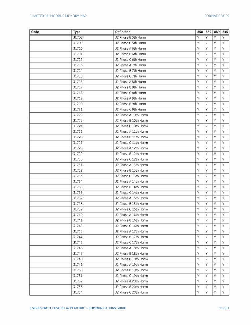
CHAPTER 11: MODBUS MEMORY MAP FORMAT CODES
31708 J2 Phase B 5th Harm Y Y Y Y
31709 J2 Phase C 5th Harm Y Y Y Y
31710 J2 Phase A 6th Harm Y Y Y Y
31711 J2 Phase B 6th Harm Y Y Y Y
31712 J2 Phase C 6th Harm Y Y Y Y
31713 J2 Phase A 7th Harm Y Y Y Y
31714 J2 Phase B 7th Harm Y Y Y Y
31715 J2 Phase C 7th Harm Y Y Y Y
31716 J2 Phase A 8th Harm Y Y Y Y
31717 J2 Phase B 8th Harm Y Y Y Y
31718 J2 Phase C 8th Harm Y Y Y Y
31719 J2 Phase A 9th Harm Y Y Y Y
31720 J2 Phase B 9th Harm Y Y Y Y
31721 J2 Phase C 9th Harm Y Y Y Y
31722 J2 Phase A 10th Harm Y Y Y Y
31723 J2 Phase B 10th Harm Y Y Y Y
31724 J2 Phase C 10th Harm Y Y Y Y
31725 J2 Phase A 11th Harm Y Y Y Y
31726 J2 Phase B 11th Harm Y Y Y Y
31727 J2 Phase C 11th Harm Y Y Y Y
31728 J2 Phase A 12th Harm Y Y Y Y
31729 J2 Phase B 12th Harm Y Y Y Y
31730 J2 Phase C 12th Harm Y Y Y Y
31731 J2 Phase A 13th Harm Y Y Y Y
31732 J2 Phase B 13th Harm Y Y Y Y
31733 J2 Phase C 13th Harm Y Y Y Y
31734 J2 Phase A 14th Harm Y Y Y Y
31735 J2 Phase B 14th Harm Y Y Y Y
31736 J2 Phase C 14th Harm Y Y Y Y
31737 J2 Phase A 15th Harm Y Y Y Y
31738 J2 Phase B 15th Harm Y Y Y Y
31739 J2 Phase C 15th Harm Y Y Y Y
31740 J2 Phase A 16th Harm Y Y Y Y
31741 J2 Phase B 16th Harm Y Y Y Y
31742 J2 Phase C 16th Harm Y Y Y Y
31743 J2 Phase A 17th Harm Y Y Y Y
31744 J2 Phase B 17th Harm Y Y Y Y
31745 J2 Phase C 17th Harm Y Y Y Y
31746 J2 Phase A 18th Harm Y Y Y Y
31747 J2 Phase B 18th Harm Y Y Y Y
31748 J2 Phase C 18th Harm Y Y Y Y
31749 J2 Phase A 19th Harm Y Y Y Y
31750 J2 Phase B 19th Harm Y Y Y Y
31751 J2 Phase C 19th Harm Y Y Y Y
31752 J2 Phase A 20th Harm Y Y Y Y
31753 J2 Phase B 20th Harm Y Y Y Y
31754 J2 Phase C 20th Harm Y Y Y Y
Code Type Definition 850 869 889 845
8 SERIES PROTECTIVE RELAY PLATFORM – COMMUNICATIONS GUIDE 11-353
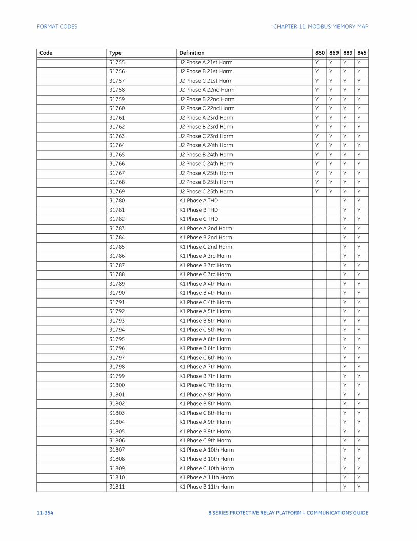
FORMAT CODES CHAPTER 11: MODBUS MEMORY MAP
31755 J2 Phase A 21st Harm Y Y Y Y
31756 J2 Phase B 21st Harm Y Y Y Y
31757 J2 Phase C 21st Harm Y Y Y Y
31758 J2 Phase A 22nd Harm Y Y Y Y
31759 J2 Phase B 22nd Harm Y Y Y Y
31760 J2 Phase C 22nd Harm Y Y Y Y
31761 J2 Phase A 23rd Harm Y Y Y Y
31762 J2 Phase B 23rd Harm Y Y Y Y
31763 J2 Phase C 23rd Harm Y Y Y Y
31764 J2 Phase A 24th Harm Y Y Y Y
31765 J2 Phase B 24th Harm Y Y Y Y
31766 J2 Phase C 24th Harm Y Y Y Y
31767 J2 Phase A 25th Harm Y Y Y Y
31768 J2 Phase B 25th Harm Y Y Y Y
31769 J2 Phase C 25th Harm Y Y Y Y
31780 K1 Phase A THD Y Y
31781 K1 Phase B THD Y Y
31782 K1 Phase C THD Y Y
31783 K1 Phase A 2nd Harm Y Y
31784 K1 Phase B 2nd Harm Y Y
31785 K1 Phase C 2nd Harm Y Y
31786 K1 Phase A 3rd Harm Y Y
31787 K1 Phase B 3rd Harm Y Y
31788 K1 Phase C 3rd Harm Y Y
31789 K1 Phase A 4th Harm Y Y
31790 K1 Phase B 4th Harm Y Y
31791 K1 Phase C 4th Harm Y Y
31792 K1 Phase A 5th Harm Y Y
31793 K1 Phase B 5th Harm Y Y
31794 K1 Phase C 5th Harm Y Y
31795 K1 Phase A 6th Harm Y Y
31796 K1 Phase B 6th Harm Y Y
31797 K1 Phase C 6th Harm Y Y
31798 K1 Phase A 7th Harm Y Y
31799 K1 Phase B 7th Harm Y Y
31800 K1 Phase C 7th Harm Y Y
31801 K1 Phase A 8th Harm Y Y
31802 K1 Phase B 8th Harm Y Y
31803 K1 Phase C 8th Harm Y Y
31804 K1 Phase A 9th Harm Y Y
31805 K1 Phase B 9th Harm Y Y
31806 K1 Phase C 9th Harm Y Y
31807 K1 Phase A 10th Harm Y Y
31808 K1 Phase B 10th Harm Y Y
31809 K1 Phase C 10th Harm Y Y
31810 K1 Phase A 11th Harm Y Y
31811 K1 Phase B 11th Harm Y Y
Code Type Definition 850 869 889 845
11-354 8 SERIES PROTECTIVE RELAY PLATFORM – COMMUNICATIONS GUIDE
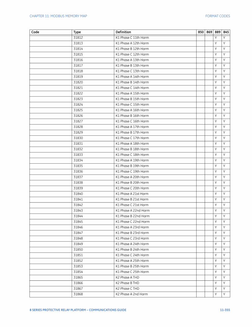
CHAPTER 11: MODBUS MEMORY MAP FORMAT CODES
31812 K1 Phase C 11th Harm Y Y
31813 K1 Phase A 12th Harm Y Y
31814 K1 Phase B 12th Harm Y Y
31815 K1 Phase C 12th Harm Y Y
31816 K1 Phase A 13th Harm Y Y
31817 K1 Phase B 13th Harm Y Y
31818 K1 Phase C 13th Harm Y Y
31819 K1 Phase A 14th Harm Y Y
31820 K1 Phase B 14th Harm Y Y
31821 K1 Phase C 14th Harm Y Y
31822 K1 Phase A 15th Harm Y Y
31823 K1 Phase B 15th Harm Y Y
31824 K1 Phase C 15th Harm Y Y
31825 K1 Phase A 16th Harm Y Y
31826 K1 Phase B 16th Harm Y Y
31827 K1 Phase C 16th Harm Y Y
31828 K1 Phase A 17th Harm Y Y
31829 K1 Phase B 17th Harm Y Y
31830 K1 Phase C 17th Harm Y Y
31831 K1 Phase A 18th Harm Y Y
31832 K1 Phase B 18th Harm Y Y
31833 K1 Phase C 18th Harm Y Y
31834 K1 Phase A 19th Harm Y Y
31835 K1 Phase B 19th Harm Y Y
31836 K1 Phase C 19th Harm Y Y
31837 K1 Phase A 20th Harm Y Y
31838 K1 Phase B 20th Harm Y Y
31839 K1 Phase C 20th Harm Y Y
31840 K1 Phase A 21st Harm Y Y
31841 K1 Phase B 21st Harm Y Y
31842 K1 Phase C 21st Harm Y Y
31843 K1 Phase A 22nd Harm Y Y
31844 K1 Phase B 22nd Harm Y Y
31845 K1 Phase C 22nd Harm Y Y
31846 K1 Phase A 23rd Harm Y Y
31847 K1 Phase B 23rd Harm Y Y
31848 K1 Phase C 23rd Harm Y Y
31849 K1 Phase A 24th Harm Y Y
31850 K1 Phase B 24th Harm Y Y
31851 K1 Phase C 24th Harm Y Y
31852 K1 Phase A 25th Harm Y Y
31853 K1 Phase B 25th Harm Y Y
31854 K1 Phase C 25th Harm Y Y
31865 K2 Phase A THD Y Y
31866 K2 Phase B THD Y Y
31867 K2 Phase C THD Y Y
31868 K2 Phase A 2nd Harm Y Y
Code Type Definition 850 869 889 845
8 SERIES PROTECTIVE RELAY PLATFORM – COMMUNICATIONS GUIDE 11-355
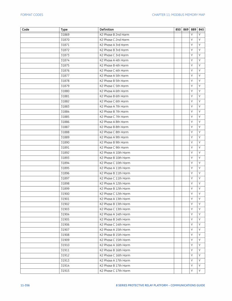
FORMAT CODES CHAPTER 11: MODBUS MEMORY MAP
31869 K2 Phase B 2nd Harm Y Y
31870 K2 Phase C 2nd Harm Y Y
31871 K2 Phase A 3rd Harm Y Y
31872 K2 Phase B 3rd Harm Y Y
31873 K2 Phase C 3rd Harm Y Y
31874 K2 Phase A 4th Harm Y Y
31875 K2 Phase B 4th Harm Y Y
31876 K2 Phase C 4th Harm Y Y
31877 K2 Phase A 5th Harm Y Y
31878 K2 Phase B 5th Harm Y Y
31879 K2 Phase C 5th Harm Y Y
31880 K2 Phase A 6th Harm Y Y
31881 K2 Phase B 6th Harm Y Y
31882 K2 Phase C 6th Harm Y Y
31883 K2 Phase A 7th Harm Y Y
31884 K2 Phase B 7th Harm Y Y
31885 K2 Phase C 7th Harm Y Y
31886 K2 Phase A 8th Harm Y Y
31887 K2 Phase B 8th Harm Y Y
31888 K2 Phase C 8th Harm Y Y
31889 K2 Phase A 9th Harm Y Y
31890 K2 Phase B 9th Harm Y Y
31891 K2 Phase C 9th Harm Y Y
31892 K2 Phase A 10th Harm Y Y
31893 K2 Phase B 10th Harm Y Y
31894 K2 Phase C 10th Harm Y Y
31895 K2 Phase A 11th Harm Y Y
31896 K2 Phase B 11th Harm Y Y
31897 K2 Phase C 11th Harm Y Y
31898 K2 Phase A 12th Harm Y Y
31899 K2 Phase B 12th Harm Y Y
31900 K2 Phase C 12th Harm Y Y
31901 K2 Phase A 13th Harm Y Y
31902 K2 Phase B 13th Harm Y Y
31903 K2 Phase C 13th Harm Y Y
31904 K2 Phase A 14th Harm Y Y
31905 K2 Phase B 14th Harm Y Y
31906 K2 Phase C 14th Harm Y Y
31907 K2 Phase A 15th Harm Y Y
31908 K2 Phase B 15th Harm Y Y
31909 K2 Phase C 15th Harm Y Y
31910 K2 Phase A 16th Harm Y Y
31911 K2 Phase B 16th Harm Y Y
31912 K2 Phase C 16th Harm Y Y
31913 K2 Phase A 17th Harm Y Y
31914 K2 Phase B 17th Harm Y Y
31915 K2 Phase C 17th Harm Y Y
Code Type Definition 850 869 889 845
11-356 8 SERIES PROTECTIVE RELAY PLATFORM – COMMUNICATIONS GUIDE
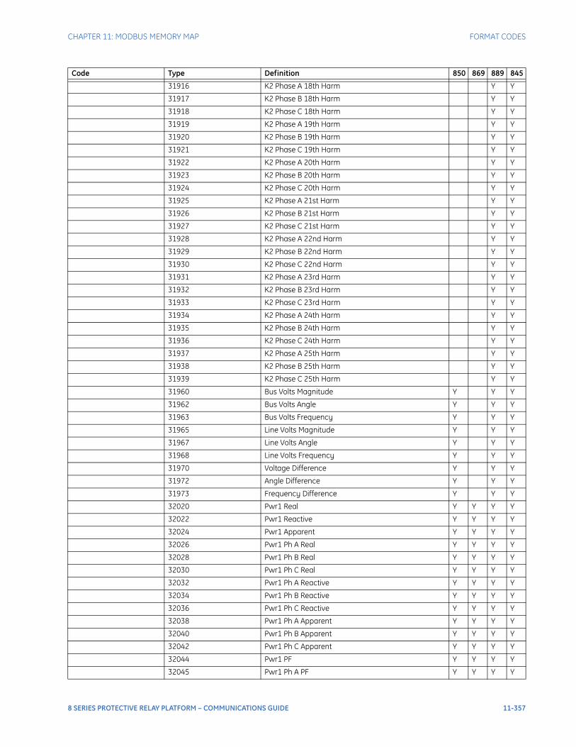
CHAPTER 11: MODBUS MEMORY MAP FORMAT CODES
31916 K2 Phase A 18th Harm Y Y
31917 K2 Phase B 18th Harm Y Y
31918 K2 Phase C 18th Harm Y Y
31919 K2 Phase A 19th Harm Y Y
31920 K2 Phase B 19th Harm Y Y
31921 K2 Phase C 19th Harm Y Y
31922 K2 Phase A 20th Harm Y Y
31923 K2 Phase B 20th Harm Y Y
31924 K2 Phase C 20th Harm Y Y
31925 K2 Phase A 21st Harm Y Y
31926 K2 Phase B 21st Harm Y Y
31927 K2 Phase C 21st Harm Y Y
31928 K2 Phase A 22nd Harm Y Y
31929 K2 Phase B 22nd Harm Y Y
31930 K2 Phase C 22nd Harm Y Y
31931 K2 Phase A 23rd Harm Y Y
31932 K2 Phase B 23rd Harm Y Y
31933 K2 Phase C 23rd Harm Y Y
31934 K2 Phase A 24th Harm Y Y
31935 K2 Phase B 24th Harm Y Y
31936 K2 Phase C 24th Harm Y Y
31937 K2 Phase A 25th Harm Y Y
31938 K2 Phase B 25th Harm Y Y
31939 K2 Phase C 25th Harm Y Y
31960 Bus Volts Magnitude Y Y Y
31962 Bus Volts Angle Y Y Y
31963 Bus Volts Frequency Y Y Y
31965 Line Volts Magnitude Y Y Y
31967 Line Volts Angle Y Y Y
31968 Line Volts Frequency Y Y Y
31970 Voltage Difference Y Y Y
31972 Angle Difference Y Y Y
31973 Frequency Difference Y Y Y
32020 Pwr1 Real Y Y Y Y
32022 Pwr1 Reactive Y Y Y Y
32024 Pwr1 Apparent Y Y Y Y
32026 Pwr1 Ph A Real Y Y Y Y
32028 Pwr1 Ph B Real Y Y Y Y
32030 Pwr1 Ph C Real Y Y Y Y
32032 Pwr1 Ph A Reactive Y Y Y Y
32034 Pwr1 Ph B Reactive Y Y Y Y
32036 Pwr1 Ph C Reactive Y Y Y Y
32038 Pwr1 Ph A Apparent Y Y Y Y
32040 Pwr1 Ph B Apparent Y Y Y Y
32042 Pwr1 Ph C Apparent Y Y Y Y
32044 Pwr1 PF Y Y Y Y
32045 Pwr1 Ph A PF Y Y Y Y
Code Type Definition 850 869 889 845
8 SERIES PROTECTIVE RELAY PLATFORM – COMMUNICATIONS GUIDE 11-357
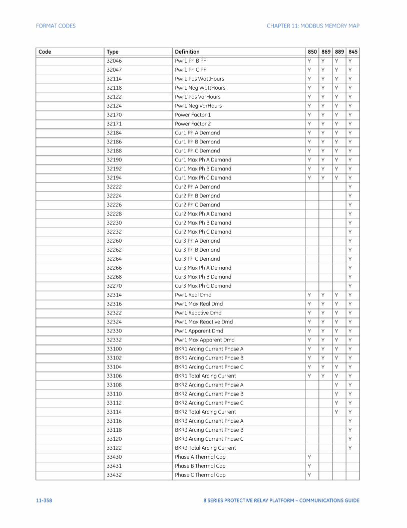
FORMAT CODES CHAPTER 11: MODBUS MEMORY MAP
32046 Pwr1 Ph B PF Y Y Y Y
32047 Pwr1 Ph C PF Y Y Y Y
32114 Pwr1 Pos WattHours Y Y Y Y
32118 Pwr1 Neg WattHours Y Y Y Y
32122 Pwr1 Pos VarHours Y Y Y Y
32124 Pwr1 Neg VarHours Y Y Y Y
32170 Power Factor 1 Y Y Y Y
32171 Power Factor 2 Y Y Y Y
32184 Cur1 Ph A Demand Y Y Y Y
32186 Cur1 Ph B Demand Y Y Y Y
32188 Cur1 Ph C Demand Y Y Y Y
32190 Cur1 Max Ph A Demand Y Y Y Y
32192 Cur1 Max Ph B Demand Y Y Y Y
32194 Cur1 Max Ph C Demand Y Y Y Y
32222 Cur2 Ph A Demand Y
32224 Cur2 Ph B Demand Y
32226 Cur2 Ph C Demand Y
32228 Cur2 Max Ph A Demand Y
32230 Cur2 Max Ph B Demand Y
32232 Cur2 Max Ph C Demand Y
32260 Cur3 Ph A Demand Y
32262 Cur3 Ph B Demand Y
32264 Cur3 Ph C Demand Y
32266 Cur3 Max Ph A Demand Y
32268 Cur3 Max Ph B Demand Y
32270 Cur3 Max Ph C Demand Y
32314 Pwr1 Real Dmd Y Y Y Y
32316 Pwr1 Max Real Dmd Y Y Y Y
32322 Pwr1 Reactive Dmd Y Y Y Y
32324 Pwr1 Max Reactive Dmd Y Y Y Y
32330 Pwr1 Apparent Dmd Y Y Y Y
32332 Pwr1 Max Apparent Dmd Y Y Y Y
33100 BKR1 Arcing Current Phase A Y Y Y Y
33102 BKR1 Arcing Current Phase B Y Y Y Y
33104 BKR1 Arcing Current Phase C Y Y Y Y
33106 BKR1 Total Arcing Current Y Y Y Y
33108 BKR2 Arcing Current Phase A Y Y
33110 BKR2 Arcing Current Phase B Y Y
33112 BKR2 Arcing Current Phase C Y Y
33114 BKR2 Total Arcing Current Y Y
33116 BKR3 Arcing Current Phase A Y
33118 BKR3 Arcing Current Phase B Y
33120 BKR3 Arcing Current Phase C Y
33122 BKR3 Total Arcing Current Y
33430 Phase A Thermal Cap Y
33431 Phase B Thermal Cap Y
33432 Phase C Thermal Cap Y
Code Type Definition 850 869 889 845
11-358 8 SERIES PROTECTIVE RELAY PLATFORM – COMMUNICATIONS GUIDE
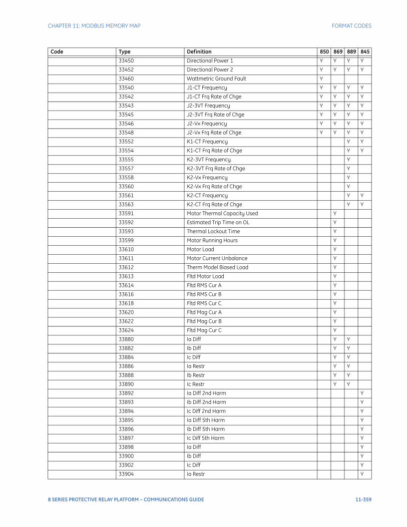
CHAPTER 11: MODBUS MEMORY MAP FORMAT CODES
33450 Directional Power 1 Y Y Y Y
33452 Directional Power 2 Y Y Y Y
33460 Wattmetric Ground Fault Y
33540 J1-CT Frequency Y Y Y Y
33542 J1-CT Frq Rate of Chge Y Y Y Y
33543 J2-3VT Frequency Y Y Y Y
33545 J2-3VT Frq Rate of Chge Y Y Y Y
33546 J2-Vx Frequency Y Y Y Y
33548 J2-Vx Frq Rate of Chge Y Y Y Y
33552 K1-CT Frequency Y Y
33554 K1-CT Frq Rate of Chge Y Y
33555 K2-3VT Frequency Y
33557 K2-3VT Frq Rate of Chge Y
33558 K2-Vx Frequency Y
33560 K2-Vx Frq Rate of Chge Y
33561 K2-CT Frequency Y Y
33563 K2-CT Frq Rate of Chge Y Y
33591 Motor Thermal Capacity Used Y
33592 Estimated Trip Time on OL Y
33593 Thermal Lockout Time Y
33599 Motor Running Hours Y
33610 Motor Load Y
33611 Motor Current Unbalance Y
33612 Therm Model Biased Load Y
33613 Fltd Motor Load Y
33614 Fltd RMS Cur A Y
33616 Fltd RMS Cur B Y
33618 Fltd RMS Cur C Y
33620 Fltd Mag Cur A Y
33622 Fltd Mag Cur B Y
33624 Fltd Mag Cur C Y
33880 Ia Diff Y Y
33882 Ib Diff Y Y
33884 Ic Diff Y Y
33886 Ia Restr Y Y
33888 Ib Restr Y Y
33890 Ic Restr Y Y
33892 Ia Diff 2nd Harm Y
33893 Ib Diff 2nd Harm Y
33894 Ic Diff 2nd Harm Y
33895 Ia Diff 5th Harm Y
33896 Ib Diff 5th Harm Y
33897 Ic Diff 5th Harm Y
33898 Ia Diff Y
33900 Ib Diff Y
33902 Ic Diff Y
33904 Ia Restr Y
Code Type Definition 850 869 889 845
8 SERIES PROTECTIVE RELAY PLATFORM – COMMUNICATIONS GUIDE 11-359
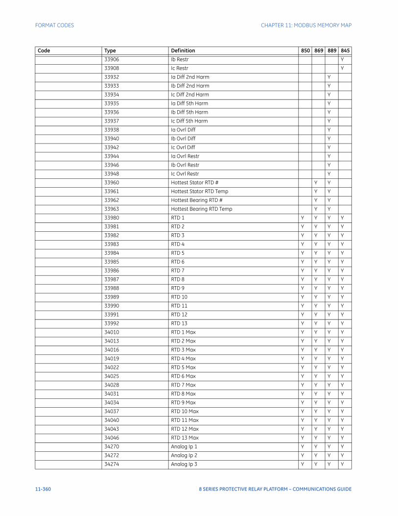
FORMAT CODES CHAPTER 11: MODBUS MEMORY MAP
33906 Ib Restr Y
33908 Ic Restr Y
33932 Ia Diff 2nd Harm Y
33933 Ib Diff 2nd Harm Y
33934 Ic Diff 2nd Harm Y
33935 Ia Diff 5th Harm Y
33936 Ib Diff 5th Harm Y
33937 Ic Diff 5th Harm Y
33938 Ia Ovrl Diff Y
33940 Ib Ovrl Diff Y
33942 Ic Ovrl Diff Y
33944 Ia Ovrl Restr Y
33946 Ib Ovrl Restr Y
33948 Ic Ovrl Restr Y
33960 Hottest Stator RTD # Y Y
33961 Hottest Stator RTD Temp Y Y
33962 Hottest Bearing RTD # Y Y
33963 Hottest Bearing RTD Temp Y Y
33980 RTD 1 Y Y Y Y
33981 RTD 2 Y Y Y Y
33982 RTD 3 Y Y Y Y
33983 RTD 4 Y Y Y Y
33984 RTD 5 Y Y Y Y
33985 RTD 6 Y Y Y Y
33986 RTD 7 Y Y Y Y
33987 RTD 8 Y Y Y Y
33988 RTD 9 Y Y Y Y
33989 RTD 10 Y Y Y Y
33990 RTD 11 Y Y Y Y
33991 RTD 12 Y Y Y Y
33992 RTD 13 Y Y Y Y
34010 RTD 1 Max Y Y Y Y
34013 RTD 2 Max Y Y Y Y
34016 RTD 3 Max Y Y Y Y
34019 RTD 4 Max Y Y Y Y
34022 RTD 5 Max Y Y Y Y
34025 RTD 6 Max Y Y Y Y
34028 RTD 7 Max Y Y Y Y
34031 RTD 8 Max Y Y Y Y
34034 RTD 9 Max Y Y Y Y
34037 RTD 10 Max Y Y Y Y
34040 RTD 11 Max Y Y Y Y
34043 RTD 12 Max Y Y Y Y
34046 RTD 13 Max Y Y Y Y
34270 Analog Ip 1 Y Y Y Y
34272 Analog Ip 2 Y Y Y Y
34274 Analog Ip 3 Y Y Y Y
Code Type Definition 850 869 889 845
11-360 8 SERIES PROTECTIVE RELAY PLATFORM – COMMUNICATIONS GUIDE
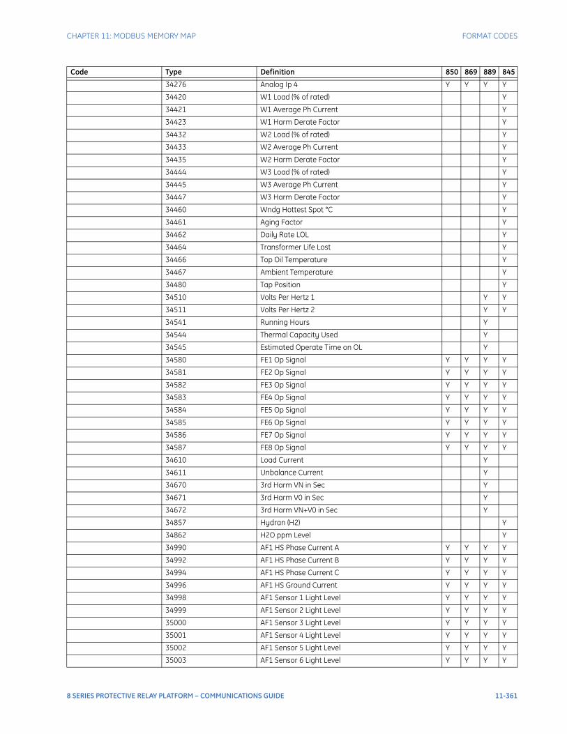
CHAPTER 11: MODBUS MEMORY MAP FORMAT CODES
34276 Analog Ip 4 Y Y Y Y
34420 W1 Load (% of rated) Y
34421 W1 Average Ph Current Y
34423 W1 Harm Derate Factor Y
34432 W2 Load (% of rated) Y
34433 W2 Average Ph Current Y
34435 W2 Harm Derate Factor Y
34444 W3 Load (% of rated) Y
34445 W3 Average Ph Current Y
34447 W3 Harm Derate Factor Y
34460 Wndg Hottest Spot °C Y
34461 Aging Factor Y
34462 Daily Rate LOL Y
34464 Transformer Life Lost Y
34466 Top Oil Temperature Y
34467 Ambient Temperature Y
34480 Tap Position Y
34510 Volts Per Hertz 1 Y Y
34511 Volts Per Hertz 2 Y Y
34541 Running Hours Y
34544 Thermal Capacity Used Y
34545 Estimated Operate Time on OL Y
34580 FE1 Op Signal Y Y Y Y
34581 FE2 Op Signal Y Y Y Y
34582 FE3 Op Signal Y Y Y Y
34583 FE4 Op Signal Y Y Y Y
34584 FE5 Op Signal Y Y Y Y
34585 FE6 Op Signal Y Y Y Y
34586 FE7 Op Signal Y Y Y Y
34587 FE8 Op Signal Y Y Y Y
34610 Load Current Y
34611 Unbalance Current Y
34670 3rd Harm VN in Sec Y
34671 3rd Harm V0 in Sec Y
34672 3rd Harm VN+V0 in Sec Y
34857 Hydran (H2) Y
34862 H2O ppm Level Y
34990 AF1 HS Phase Current A Y Y Y Y
34992 AF1 HS Phase Current B Y Y Y Y
34994 AF1 HS Phase Current C Y Y Y Y
34996 AF1 HS Ground Current Y Y Y Y
34998 AF1 Sensor 1 Light Level Y Y Y Y
34999 AF1 Sensor 2 Light Level Y Y Y Y
35000 AF1 Sensor 3 Light Level Y Y Y Y
35001 AF1 Sensor 4 Light Level Y Y Y Y
35002 AF1 Sensor 5 Light Level Y Y Y Y
35003 AF1 Sensor 6 Light Level Y Y Y Y
Code Type Definition 850 869 889 845
8 SERIES PROTECTIVE RELAY PLATFORM – COMMUNICATIONS GUIDE 11-361
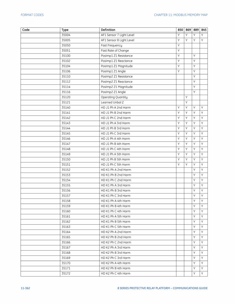
FORMAT CODES CHAPTER 11: MODBUS MEMORY MAP
35004 AF1 Sensor 7 Light Level Y Y Y Y
35005 AF1 Sensor 8 Light Level Y Y Y Y
35050 Fast Frequency Y
35051 Fast Rate of Change Y
35100 PosImp1 Z1 Resistance Y Y
35102 PosImp1 Z1 Reactance Y Y
35104 PosImp1 Z1 Magnitude Y Y
35106 PosImp1 Z1 Angle Y Y
35110 PosImp2 Z1 Resistance Y
35112 PosImp2 Z1 Reactance Y
35114 PosImp2 Z1 Magnitude Y
35116 PosImp2 Z1 Angle Y
35120 Operating Quantity Y
35121 Learned Unbal Z Y
35140 HD J1 Ph A 2nd Harm Y Y Y Y
35141 HD J1 Ph B 2nd Harm Y Y Y Y
35142 HD J1 Ph C 2nd Harm Y Y Y Y
35143 HD J1 Ph A 3rd Harm Y Y Y Y
35144 HD J1 Ph B 3rd Harm Y Y Y Y
35145 HD J1 Ph C 3rd Harm Y Y Y Y
35146 HD J1 Ph A 4th Harm Y Y Y Y
35147 HD J1 Ph B 4th Harm Y Y Y Y
35148 HD J1 Ph C 4th Harm Y Y Y Y
35149 HD J1 Ph A 5th Harm Y Y Y Y
35150 HD J1 Ph B 5th Harm Y Y Y Y
35151 HD J1 Ph C 5th Harm Y Y Y Y
35152 HD K1 Ph A 2nd Harm Y Y
35153 HD K1 Ph B 2nd Harm Y Y
35154 HD K1 Ph C 2nd Harm Y Y
35155 HD K1 Ph A 3rd Harm Y Y
35156 HD K1 Ph B 3rd Harm Y Y
35157 HD K1 Ph C 3rd Harm Y Y
35158 HD K1 Ph A 4th Harm Y Y
35159 HD K1 Ph B 4th Harm Y Y
35160 HD K1 Ph C 4th Harm Y Y
35161 HD K1 Ph A 5th Harm Y Y
35162 HD K1 Ph B 5th Harm Y Y
35163 HD K1 Ph C 5th Harm Y Y
35164 HD K2 Ph A 2nd Harm Y Y
35165 HD K2 Ph B 2nd Harm Y Y
35166 HD K2 Ph C 2nd Harm Y Y
35167 HD K2 Ph A 3rd Harm Y Y
35168 HD K2 Ph B 3rd Harm Y Y
35169 HD K2 Ph C 3rd Harm Y Y
35170 HD K2 Ph A 4th Harm Y Y
35171 HD K2 Ph B 4th Harm Y Y
35172 HD K2 Ph C 4th Harm Y Y
Code Type Definition 850 869 889 845
11-362 8 SERIES PROTECTIVE RELAY PLATFORM – COMMUNICATIONS GUIDE
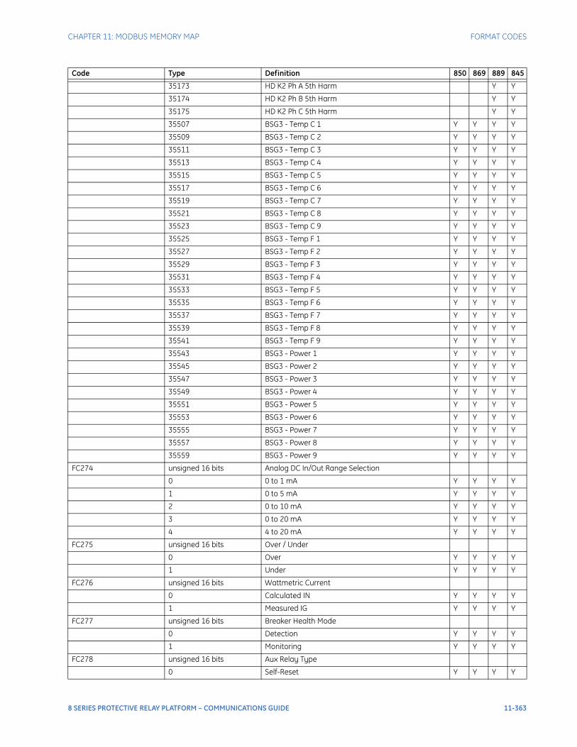
CHAPTER 11: MODBUS MEMORY MAP FORMAT CODES
35173 HD K2 Ph A 5th Harm Y Y
35174 HD K2 Ph B 5th Harm Y Y
35175 HD K2 Ph C 5th Harm Y Y
35507 BSG3 - Temp C 1 Y Y Y Y
35509 BSG3 - Temp C 2 Y Y Y Y
35511 BSG3 - Temp C 3 Y Y Y Y
35513 BSG3 - Temp C 4 Y Y Y Y
35515 BSG3 - Temp C 5 Y Y Y Y
35517 BSG3 - Temp C 6 Y Y Y Y
35519 BSG3 - Temp C 7 Y Y Y Y
35521 BSG3 - Temp C 8 Y Y Y Y
35523 BSG3 - Temp C 9 Y Y Y Y
35525 BSG3 - Temp F 1 Y Y Y Y
35527 BSG3 - Temp F 2 Y Y Y Y
35529 BSG3 - Temp F 3 Y Y Y Y
35531 BSG3 - Temp F 4 Y Y Y Y
35533 BSG3 - Temp F 5 Y Y Y Y
35535 BSG3 - Temp F 6 Y Y Y Y
35537 BSG3 - Temp F 7 Y Y Y Y
35539 BSG3 - Temp F 8 Y Y Y Y
35541 BSG3 - Temp F 9 Y Y Y Y
35543 BSG3 - Power 1 Y Y Y Y
35545 BSG3 - Power 2 Y Y Y Y
35547 BSG3 - Power 3 Y Y Y Y
35549 BSG3 - Power 4 Y Y Y Y
35551 BSG3 - Power 5 Y Y Y Y
35553 BSG3 - Power 6 Y Y Y Y
35555 BSG3 - Power 7 Y Y Y Y
35557 BSG3 - Power 8 Y Y Y Y
35559 BSG3 - Power 9 Y Y Y Y
FC274 unsigned 16 bits Analog DC In/Out Range Selection
0 0 to 1 mA Y Y Y Y
1 0 to 5 mA Y Y Y Y
2 0 to 10 mA Y Y Y Y
3 0 to 20 mA Y Y Y Y
4 4 to 20 mA Y Y Y Y
FC275 unsigned 16 bits Over / Under
0 Over Y Y Y Y
1 Under Y Y Y Y
FC276 unsigned 16 bits Wattmetric Current
0 Calculated IN Y Y Y Y
1 Measured IG Y Y Y Y
FC277 unsigned 16 bits Breaker Health Mode
0 Detection Y Y Y Y
1 Monitoring Y Y Y Y
FC278 unsigned 16 bits Aux Relay Type
0 Self-Reset Y Y Y Y
Code Type Definition 850 869 889 845
8 SERIES PROTECTIVE RELAY PLATFORM – COMMUNICATIONS GUIDE 11-363

FORMAT CODES CHAPTER 11: MODBUS MEMORY MAP
1 Latched Y Y Y Y
2 Pulsed Y Y Y Y
FC279 unsigned 16 bits UV Restoration Initiation
0 Off Y Y Y Y
1 Ph UV 1 OP Y Y Y Y
2 Ph UV 2 OP Y Y Y Y
3 Aux UV 1 OP Y Y Y Y
4 Aux UV 2 OP Y Y Y Y
FC280 unsigned 16 bits Close Syncrocheck Supervision
0 Bypass Y Y Y Y
1 Sync1 Close Perm Y Y Y Y
FC283 unsigned 16 bits Synchrocheck Dead Source Permit
0 Disabled Y Y Y
1 LB & DL Y Y Y
2 DB & LL Y Y Y
3 DB & DL Y Y Y
4 DB OR DL Y Y Y
5 DB XOR DL Y Y Y
FC284 unsigned 16 bits Transfer Function Scheme
0 Disabled Y Y Y Y
1 Incomer 1 Y Y Y Y
2 Incomer 2 Y Y Y Y
3 Bus Tie Y Y Y Y
FC286 unsigned 16 bits Power Factor Power Input
0 Power 1 Y
1 Power 2 Y
FC287 unsigned 16 bits UF Restoration Initiation
0 Off Y
1 UnderFreq 1 OP Y
2 UnderFreq 2 OP Y
3 UnderFreq 3 OP Y
4 UnderFreq 4 OP Y
5 UnderFreq 5 OP Y
6 UnderFreq 6 OP Y
7 Freq ROC 1 DWN OP Y
8 Freq ROC 2 DWN OP Y
9 Freq ROC 3 DWN OP Y
10 Freq ROC 4 DWN OP Y
11 Freq ROC 5 DWN OP Y
12 Freq ROC 6 DWN OP Y
FC288 unsigned 16 bits Three State Security Model
0 No Security Y Y Y Y
1 Passwords Enabled Y Y Y Y
2 Full Security Y Y Y Y
FC289 unsigned 16 bits Breaker Status
0 Not Set Y Y Y Y
1 Fail Y Y Y Y
Code Type Definition 850 869 889 845
11-364 8 SERIES PROTECTIVE RELAY PLATFORM – COMMUNICATIONS GUIDE

CHAPTER 11: MODBUS MEMORY MAP FORMAT CODES
2 OK Y Y Y Y
FC290 unsigned 16 bits Default Screen Index
0 Off Y Y Y Y
7 BKR1 Y Y Y Y
8 BKR2 Y Y Y Y
9 BKR3 Y Y Y Y
11 CONT Y Y Y Y
15 AF 1 Y Y Y Y
16 AF 2 Y Y Y Y
17 AF 3 Y Y Y Y
18 Inputs Y Y Y Y
19 Relays Y Y Y Y
20 V Inputs Y Y Y Y
21 V Outpts Y Y Y Y
30 Info Y Y Y Y
34 Dev Stat Y Y Y Y
35 Clock Y Y Y Y
36 PTP Y Y Y Y
37 Fault Loc Y Y Y Y
39 Arcing I Y Y Y Y
42 Values Y Y Y Y
43 SLD Y Y Y Y
44 Phasor J Y Y Y Y
45 Seq J Y Y Y Y
46 Phasor K Y Y Y Y
47 Seq K Y Y Y Y
68 CT1-J1 Y Y Y Y
69 CT2-K1 Y Y Y Y
70 CT3-K2 Y Y Y Y
71 VT1-J2 Y Y Y Y
72 VT2-K2 Y Y Y Y
73 VT1x-J2 Y Y Y Y
74 VT2x-K2 Y Y Y Y
79 Harm1-J1 Y Y Y Y
80 Harm2-J2 Y Y Y Y
81 Harm3-K1 Y Y Y Y
82 Harm4-K2 Y Y Y Y
86 Power 1 Y Y Y Y
87 Power 2 Y Y Y Y
88 Energy 1 Y Y Y Y
89 Energy 2 Y Y Y Y
91 CurDmnd 1 Y Y Y Y
92 CurDmnd 2 Y Y Y Y
93 CurDmnd 3 Y Y Y Y
94 Pwr Dmd1 Y Y Y Y
95 Pwr Dmd2 Y Y Y Y
FC300 unsigned 32 bits LEDs 1-16
Code Type Definition 850 869 889 845
8 SERIES PROTECTIVE RELAY PLATFORM – COMMUNICATIONS GUIDE 11-365

FORMAT CODES CHAPTER 11: MODBUS MEMORY MAP
0x00000000 Off Y Y Y Y
0x00000001 LED 1 Red Y Y Y Y
0x00000002 LED 1 Green Y Y Y Y
0x00000003 LED 1 Orange Y Y Y Y
0x00000004 LED 2 Red Y Y Y Y
0x00000008 LED 2 Green Y Y Y Y
0x0000000C LED 2 Orange Y Y Y Y
0x00000010 LED 3 Red Y Y Y Y
0x00000020 LED 3 Green Y Y Y Y
0x00000030 LED 3 Orange Y Y Y Y
0x00000040 LED 4 Red Y Y Y Y
0x00000080 LED 4 Green Y Y Y Y
0x000000C0 LED 4 Orange Y Y Y Y
0x00000100 LED 5 Red Y Y Y Y
0x00000200 LED 5 Green Y Y Y Y
0x00000300 LED 5 Orange Y Y Y Y
0x00000400 LED 6 Red Y Y Y Y
0x00000800 LED 6 Green Y Y Y Y
0x00000C00 LED 6 Orange Y Y Y Y
0x00001000 LED 7 Red Y Y Y Y
0x00002000 LED 7 Green Y Y Y Y
0x00003000 LED 7 Orange Y Y Y Y
0x00004000 LED 8 Red Y Y Y Y
0x00008000 LED 8 Green Y Y Y Y
0x0000C000 LED 8 Orange Y Y Y Y
0x00010000 LED 9 Red Y Y Y Y
0x00020000 LED 9 Green Y Y Y Y
0x00030000 LED 9 Orange Y Y Y Y
0x00040000 LED 10 Red Y Y Y Y
0x00080000 LED 10 Green Y Y Y Y
0x000C0000 LED 10 Orange Y Y Y Y
0x00100000 LED 11 Red Y Y Y Y
0x00200000 LED 11 Green Y Y Y Y
0x00300000 LED 11 Orange Y Y Y Y
0x00400000 LED 12 Red Y Y Y Y
0x00800000 LED 12 Green Y Y Y Y
0x00C00000 LED 12 Orange Y Y Y Y
0x01000000 LED 13 Red Y Y Y Y
0x02000000 LED 13 Green Y Y Y Y
0x03000000 LED 13 Orange Y Y Y Y
0x04000000 LED 14 Red Y Y Y Y
0x08000000 LED 14 Green Y Y Y Y
0x0C000000 LED 14 Orange Y Y Y Y
0x10000000 LED 15 Red Y Y Y Y
0x20000000 LED 15 Green Y Y Y Y
0x30000000 LED 15 Orange Y Y Y Y
0x40000000 LED 16 Red Y Y Y Y
Code Type Definition 850 869 889 845
11-366 8 SERIES PROTECTIVE RELAY PLATFORM – COMMUNICATIONS GUIDE
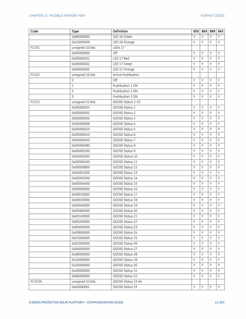
CHAPTER 11: MODBUS MEMORY MAP FORMAT CODES
0x80000000 LED 16 Green Y Y Y Y
0xC0000000 LED 16 Orange Y Y Y Y
FC301 unsigned 32 bits LEDs 17
0x00000000 Off Y Y Y Y
0x00000001 LED 17 Red Y Y Y Y
0x00000002 LED 17 Green Y Y Y Y
0x00000003 LED 17 Orange Y Y Y Y
FC322 unsigned 16 bits Active Pushbutton
0 Off Y Y Y Y
1 Pushbutton 1 ON Y Y Y Y
2 Pushbutton 2 ON Y Y Y Y
3 Pushbutton 3 ON Y Y Y Y
FC323 unsigned 32 bits GOOSE Status 1-32
0x00000001 GOOSE Status 1 Y Y Y Y
0x00000002 GOOSE Status 2 Y Y Y Y
0x00000004 GOOSE Status 3 Y Y Y Y
0x00000008 GOOSE Status 4 Y Y Y Y
0x00000010 GOOSE Status 5 Y Y Y Y
0x00000020 GOOSE Status 6 Y Y Y Y
0x00000040 GOOSE Status 7 Y Y Y Y
0x00000080 GOOSE Status 8 Y Y Y Y
0x00000100 GOOSE Status 9 Y Y Y Y
0x00000200 GOOSE Status 10 Y Y Y Y
0x00000400 GOOSE Status 11 Y Y Y Y
0x00000800 GOOSE Status 12 Y Y Y Y
0x00001000 GOOSE Status 13 Y Y Y Y
0x00002000 GOOSE Status 14 Y Y Y Y
0x00004000 GOOSE Status 15 Y Y Y Y
0x00008000 GOOSE Status 16 Y Y Y Y
0x00010000 GOOSE Status 17 Y Y Y Y
0x00020000 GOOSE Status 18 Y Y Y Y
0x00040000 GOOSE Status 19 Y Y Y Y
0x00080000 GOOSE Status 20 Y Y Y Y
0x00100000 GOOSE Status 21 Y Y Y Y
0x00200000 GOOSE Status 22 Y Y Y Y
0x00400000 GOOSE Status 23 Y Y Y Y
0x00800000 GOOSE Status 24 Y Y Y Y
0x01000000 GOOSE Status 25 Y Y Y Y
0x02000000 GOOSE Status 26 Y Y Y Y
0x04000000 GOOSE Status 27 Y Y Y Y
0x08000000 GOOSE Status 28 Y Y Y Y
0x10000000 GOOSE Status 29 Y Y Y Y
0x20000000 GOOSE Status 30 Y Y Y Y
0x40000000 GOOSE Status 31 Y Y Y Y
0x80000000 GOOSE Status 32 Y Y Y Y
FC323A unsigned 32 bits GOOSE Status 33-64
0x00000001 GOOSE Status 33 Y Y Y Y
Code Type Definition 850 869 889 845
8 SERIES PROTECTIVE RELAY PLATFORM – COMMUNICATIONS GUIDE 11-367

FORMAT CODES CHAPTER 11: MODBUS MEMORY MAP
0x00000002 GOOSE Status 34 Y Y Y Y
0x00000004 GOOSE Status 35 Y Y Y Y
0x00000008 GOOSE Status 36 Y Y Y Y
0x00000010 GOOSE Status 37 Y Y Y Y
0x00000020 GOOSE Status 38 Y Y Y Y
0x00000040 GOOSE Status 39 Y Y Y Y
0x00000080 GOOSE Status 40 Y Y Y Y
0x00000100 GOOSE Status 41 Y Y Y Y
0x00000200 GOOSE Status 42 Y Y Y Y
0x00000400 GOOSE Status 43 Y Y Y Y
0x00000800 GOOSE Status 44 Y Y Y Y
0x00001000 GOOSE Status 45 Y Y Y Y
0x00002000 GOOSE Status 46 Y Y Y Y
0x00004000 GOOSE Status 47 Y Y Y Y
0x00008000 GOOSE Status 48 Y Y Y Y
0x00010000 GOOSE Status 49 Y Y Y Y
0x00020000 GOOSE Status 50 Y Y Y Y
0x00040000 GOOSE Status 51 Y Y Y Y
0x00080000 GOOSE Status 52 Y Y Y Y
0x00100000 GOOSE Status 53 Y Y Y Y
0x00200000 GOOSE Status 54 Y Y Y Y
0x00400000 GOOSE Status 55 Y Y Y Y
0x00800000 GOOSE Status 56 Y Y Y Y
0x01000000 GOOSE Status 57 Y Y Y Y
0x02000000 GOOSE Status 58 Y Y Y Y
0x04000000 GOOSE Status 59 Y Y Y Y
0x08000000 GOOSE Status 60 Y Y Y Y
0x10000000 GOOSE Status 61 Y Y Y Y
0x20000000 GOOSE Status 62 Y Y Y Y
0x40000000 GOOSE Status 63 Y Y Y Y
0x80000000 GOOSE Status 64 Y Y Y Y
FC324 unsigned 16 bits File Transfer Mode
0 Read Y Y Y Y
1 Write Y Y Y Y
FC340 unsigned 16 bits Security Bypass Access
0 Disabled Y Y Y Y
1 Local Y Y Y Y
2 Remote Y Y Y Y
3 Local&Remote Y Y Y Y
FC341 unsigned 16 bits Radius Authentication Method
0 EAP-TTLS Y Y Y Y
FC342 unsigned 16 bits RTC Sync Source
0 None Y Y Y Y
1 Port 4 PTP Clock Y Y Y Y
2 Port 5 PTP Clock Y Y Y Y
3 IRIG B Y Y Y Y
4 SNTP Y Y Y Y
Code Type Definition 850 869 889 845
11-368 8 SERIES PROTECTIVE RELAY PLATFORM – COMMUNICATIONS GUIDE
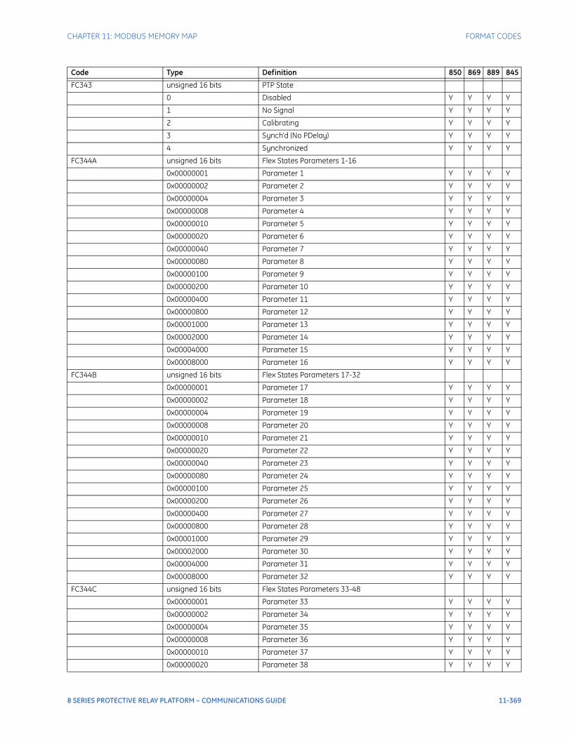
CHAPTER 11: MODBUS MEMORY MAP FORMAT CODES
FC343 unsigned 16 bits PTP State
0 Disabled Y Y Y Y
1 No Signal Y Y Y Y
2 Calibrating Y Y Y Y
3 Synch'd (No PDelay) Y Y Y Y
4 Synchronized Y Y Y Y
FC344A unsigned 16 bits Flex States Parameters 1-16
0x00000001 Parameter 1 Y Y Y Y
0x00000002 Parameter 2 Y Y Y Y
0x00000004 Parameter 3 Y Y Y Y
0x00000008 Parameter 4 Y Y Y Y
0x00000010 Parameter 5 Y Y Y Y
0x00000020 Parameter 6 Y Y Y Y
0x00000040 Parameter 7 Y Y Y Y
0x00000080 Parameter 8 Y Y Y Y
0x00000100 Parameter 9 Y Y Y Y
0x00000200 Parameter 10 Y Y Y Y
0x00000400 Parameter 11 Y Y Y Y
0x00000800 Parameter 12 Y Y Y Y
0x00001000 Parameter 13 Y Y Y Y
0x00002000 Parameter 14 Y Y Y Y
0x00004000 Parameter 15 Y Y Y Y
0x00008000 Parameter 16 Y Y Y Y
FC344B unsigned 16 bits Flex States Parameters 17-32
0x00000001 Parameter 17 Y Y Y Y
0x00000002 Parameter 18 Y Y Y Y
0x00000004 Parameter 19 Y Y Y Y
0x00000008 Parameter 20 Y Y Y Y
0x00000010 Parameter 21 Y Y Y Y
0x00000020 Parameter 22 Y Y Y Y
0x00000040 Parameter 23 Y Y Y Y
0x00000080 Parameter 24 Y Y Y Y
0x00000100 Parameter 25 Y Y Y Y
0x00000200 Parameter 26 Y Y Y Y
0x00000400 Parameter 27 Y Y Y Y
0x00000800 Parameter 28 Y Y Y Y
0x00001000 Parameter 29 Y Y Y Y
0x00002000 Parameter 30 Y Y Y Y
0x00004000 Parameter 31 Y Y Y Y
0x00008000 Parameter 32 Y Y Y Y
FC344C unsigned 16 bits Flex States Parameters 33-48
0x00000001 Parameter 33 Y Y Y Y
0x00000002 Parameter 34 Y Y Y Y
0x00000004 Parameter 35 Y Y Y Y
0x00000008 Parameter 36 Y Y Y Y
0x00000010 Parameter 37 Y Y Y Y
0x00000020 Parameter 38 Y Y Y Y
Code Type Definition 850 869 889 845
8 SERIES PROTECTIVE RELAY PLATFORM – COMMUNICATIONS GUIDE 11-369
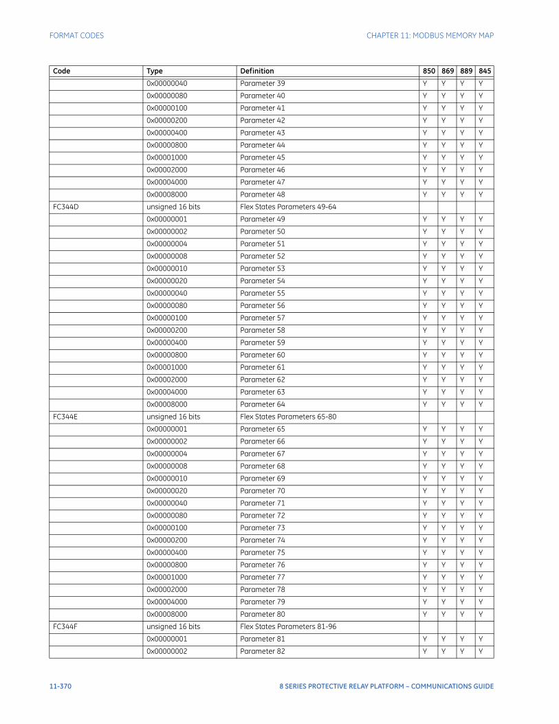
FORMAT CODES CHAPTER 11: MODBUS MEMORY MAP
0x00000040 Parameter 39 Y Y Y Y
0x00000080 Parameter 40 Y Y Y Y
0x00000100 Parameter 41 Y Y Y Y
0x00000200 Parameter 42 Y Y Y Y
0x00000400 Parameter 43 Y Y Y Y
0x00000800 Parameter 44 Y Y Y Y
0x00001000 Parameter 45 Y Y Y Y
0x00002000 Parameter 46 Y Y Y Y
0x00004000 Parameter 47 Y Y Y Y
0x00008000 Parameter 48 Y Y Y Y
FC344D unsigned 16 bits Flex States Parameters 49-64
0x00000001 Parameter 49 Y Y Y Y
0x00000002 Parameter 50 Y Y Y Y
0x00000004 Parameter 51 Y Y Y Y
0x00000008 Parameter 52 Y Y Y Y
0x00000010 Parameter 53 Y Y Y Y
0x00000020 Parameter 54 Y Y Y Y
0x00000040 Parameter 55 Y Y Y Y
0x00000080 Parameter 56 Y Y Y Y
0x00000100 Parameter 57 Y Y Y Y
0x00000200 Parameter 58 Y Y Y Y
0x00000400 Parameter 59 Y Y Y Y
0x00000800 Parameter 60 Y Y Y Y
0x00001000 Parameter 61 Y Y Y Y
0x00002000 Parameter 62 Y Y Y Y
0x00004000 Parameter 63 Y Y Y Y
0x00008000 Parameter 64 Y Y Y Y
FC344E unsigned 16 bits Flex States Parameters 65-80
0x00000001 Parameter 65 Y Y Y Y
0x00000002 Parameter 66 Y Y Y Y
0x00000004 Parameter 67 Y Y Y Y
0x00000008 Parameter 68 Y Y Y Y
0x00000010 Parameter 69 Y Y Y Y
0x00000020 Parameter 70 Y Y Y Y
0x00000040 Parameter 71 Y Y Y Y
0x00000080 Parameter 72 Y Y Y Y
0x00000100 Parameter 73 Y Y Y Y
0x00000200 Parameter 74 Y Y Y Y
0x00000400 Parameter 75 Y Y Y Y
0x00000800 Parameter 76 Y Y Y Y
0x00001000 Parameter 77 Y Y Y Y
0x00002000 Parameter 78 Y Y Y Y
0x00004000 Parameter 79 Y Y Y Y
0x00008000 Parameter 80 Y Y Y Y
FC344F unsigned 16 bits Flex States Parameters 81-96
0x00000001 Parameter 81 Y Y Y Y
0x00000002 Parameter 82 Y Y Y Y
Code Type Definition 850 869 889 845
11-370 8 SERIES PROTECTIVE RELAY PLATFORM – COMMUNICATIONS GUIDE
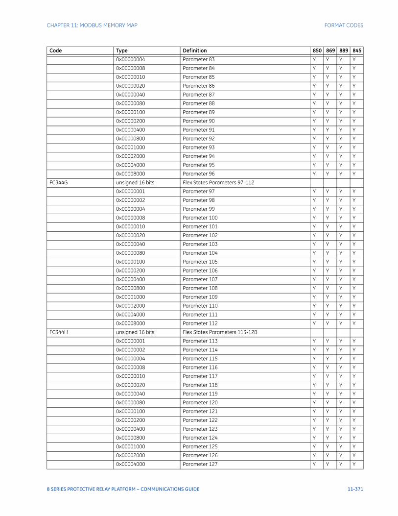
CHAPTER 11: MODBUS MEMORY MAP FORMAT CODES
0x00000004 Parameter 83 Y Y Y Y
0x00000008 Parameter 84 Y Y Y Y
0x00000010 Parameter 85 Y Y Y Y
0x00000020 Parameter 86 Y Y Y Y
0x00000040 Parameter 87 Y Y Y Y
0x00000080 Parameter 88 Y Y Y Y
0x00000100 Parameter 89 Y Y Y Y
0x00000200 Parameter 90 Y Y Y Y
0x00000400 Parameter 91 Y Y Y Y
0x00000800 Parameter 92 Y Y Y Y
0x00001000 Parameter 93 Y Y Y Y
0x00002000 Parameter 94 Y Y Y Y
0x00004000 Parameter 95 Y Y Y Y
0x00008000 Parameter 96 Y Y Y Y
FC344G unsigned 16 bits Flex States Parameters 97-112
0x00000001 Parameter 97 Y Y Y Y
0x00000002 Parameter 98 Y Y Y Y
0x00000004 Parameter 99 Y Y Y Y
0x00000008 Parameter 100 Y Y Y Y
0x00000010 Parameter 101 Y Y Y Y
0x00000020 Parameter 102 Y Y Y Y
0x00000040 Parameter 103 Y Y Y Y
0x00000080 Parameter 104 Y Y Y Y
0x00000100 Parameter 105 Y Y Y Y
0x00000200 Parameter 106 Y Y Y Y
0x00000400 Parameter 107 Y Y Y Y
0x00000800 Parameter 108 Y Y Y Y
0x00001000 Parameter 109 Y Y Y Y
0x00002000 Parameter 110 Y Y Y Y
0x00004000 Parameter 111 Y Y Y Y
0x00008000 Parameter 112 Y Y Y Y
FC344H unsigned 16 bits Flex States Parameters 113-128
0x00000001 Parameter 113 Y Y Y Y
0x00000002 Parameter 114 Y Y Y Y
0x00000004 Parameter 115 Y Y Y Y
0x00000008 Parameter 116 Y Y Y Y
0x00000010 Parameter 117 Y Y Y Y
0x00000020 Parameter 118 Y Y Y Y
0x00000040 Parameter 119 Y Y Y Y
0x00000080 Parameter 120 Y Y Y Y
0x00000100 Parameter 121 Y Y Y Y
0x00000200 Parameter 122 Y Y Y Y
0x00000400 Parameter 123 Y Y Y Y
0x00000800 Parameter 124 Y Y Y Y
0x00001000 Parameter 125 Y Y Y Y
0x00002000 Parameter 126 Y Y Y Y
0x00004000 Parameter 127 Y Y Y Y
Code Type Definition 850 869 889 845
8 SERIES PROTECTIVE RELAY PLATFORM – COMMUNICATIONS GUIDE 11-371
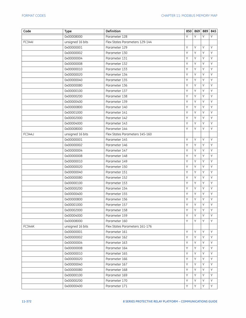
FORMAT CODES CHAPTER 11: MODBUS MEMORY MAP
0x00008000 Parameter 128 Y Y Y Y
FC344I unsigned 16 bits Flex States Parameters 129-144
0x00000001 Parameter 129 Y Y Y Y
0x00000002 Parameter 130 Y Y Y Y
0x00000004 Parameter 131 Y Y Y Y
0x00000008 Parameter 132 Y Y Y Y
0x00000010 Parameter 133 Y Y Y Y
0x00000020 Parameter 134 Y Y Y Y
0x00000040 Parameter 135 Y Y Y Y
0x00000080 Parameter 136 Y Y Y Y
0x00000100 Parameter 137 Y Y Y Y
0x00000200 Parameter 138 Y Y Y Y
0x00000400 Parameter 139 Y Y Y Y
0x00000800 Parameter 140 Y Y Y Y
0x00001000 Parameter 141 Y Y Y Y
0x00002000 Parameter 142 Y Y Y Y
0x00004000 Parameter 143 Y Y Y Y
0x00008000 Parameter 144 Y Y Y Y
FC344J unsigned 16 bits Flex States Parameters 145-160
0x00000001 Parameter 145 Y Y Y Y
0x00000002 Parameter 146 Y Y Y Y
0x00000004 Parameter 147 Y Y Y Y
0x00000008 Parameter 148 Y Y Y Y
0x00000010 Parameter 149 Y Y Y Y
0x00000020 Parameter 150 Y Y Y Y
0x00000040 Parameter 151 Y Y Y Y
0x00000080 Parameter 152 Y Y Y Y
0x00000100 Parameter 153 Y Y Y Y
0x00000200 Parameter 154 Y Y Y Y
0x00000400 Parameter 155 Y Y Y Y
0x00000800 Parameter 156 Y Y Y Y
0x00001000 Parameter 157 Y Y Y Y
0x00002000 Parameter 158 Y Y Y Y
0x00004000 Parameter 159 Y Y Y Y
0x00008000 Parameter 160 Y Y Y Y
FC344K unsigned 16 bits Flex States Parameters 161-176
0x00000001 Parameter 161 Y Y Y Y
0x00000002 Parameter 162 Y Y Y Y
0x00000004 Parameter 163 Y Y Y Y
0x00000008 Parameter 164 Y Y Y Y
0x00000010 Parameter 165 Y Y Y Y
0x00000020 Parameter 166 Y Y Y Y
0x00000040 Parameter 167 Y Y Y Y
0x00000080 Parameter 168 Y Y Y Y
0x00000100 Parameter 169 Y Y Y Y
0x00000200 Parameter 170 Y Y Y Y
0x00000400 Parameter 171 Y Y Y Y
Code Type Definition 850 869 889 845
11-372 8 SERIES PROTECTIVE RELAY PLATFORM – COMMUNICATIONS GUIDE

CHAPTER 11: MODBUS MEMORY MAP FORMAT CODES
0x00000800 Parameter 172 Y Y Y Y
0x00001000 Parameter 173 Y Y Y Y
0x00002000 Parameter 174 Y Y Y Y
0x00004000 Parameter 175 Y Y Y Y
0x00008000 Parameter 176 Y Y Y Y
FC344L unsigned 16 bits Flex States Parameters 177-192
0x00000001 Parameter 177 Y Y Y Y
0x00000002 Parameter 178 Y Y Y Y
0x00000004 Parameter 179 Y Y Y Y
0x00000008 Parameter 180 Y Y Y Y
0x00000010 Parameter 181 Y Y Y Y
0x00000020 Parameter 182 Y Y Y Y
0x00000040 Parameter 183 Y Y Y Y
0x00000080 Parameter 184 Y Y Y Y
0x00000100 Parameter 185 Y Y Y Y
0x00000200 Parameter 186 Y Y Y Y
0x00000400 Parameter 187 Y Y Y Y
0x00000800 Parameter 188 Y Y Y Y
0x00001000 Parameter 189 Y Y Y Y
0x00002000 Parameter 190 Y Y Y Y
0x00004000 Parameter 191 Y Y Y Y
0x00008000 Parameter 192 Y Y Y Y
FC344M unsigned 16 bits Flex States Parameters 193-208
0x00000001 Parameter 193 Y Y Y Y
0x00000002 Parameter 194 Y Y Y Y
0x00000004 Parameter 195 Y Y Y Y
0x00000008 Parameter 196 Y Y Y Y
0x00000010 Parameter 197 Y Y Y Y
0x00000020 Parameter 198 Y Y Y Y
0x00000040 Parameter 199 Y Y Y Y
0x00000080 Parameter 200 Y Y Y Y
0x00000100 Parameter 201 Y Y Y Y
0x00000200 Parameter 202 Y Y Y Y
0x00000400 Parameter 203 Y Y Y Y
0x00000800 Parameter 204 Y Y Y Y
0x00001000 Parameter 205 Y Y Y Y
0x00002000 Parameter 206 Y Y Y Y
0x00004000 Parameter 207 Y Y Y Y
0x00008000 Parameter 208 Y Y Y Y
FC344N unsigned 16 bits Flex States Parameters 209-224
0x00000001 Parameter 209 Y Y Y Y
0x00000002 Parameter 210 Y Y Y Y
0x00000004 Parameter 211 Y Y Y Y
0x00000008 Parameter 212 Y Y Y Y
0x00000010 Parameter 213 Y Y Y Y
0x00000020 Parameter 214 Y Y Y Y
0x00000040 Parameter 215 Y Y Y Y
Code Type Definition 850 869 889 845
8 SERIES PROTECTIVE RELAY PLATFORM – COMMUNICATIONS GUIDE 11-373
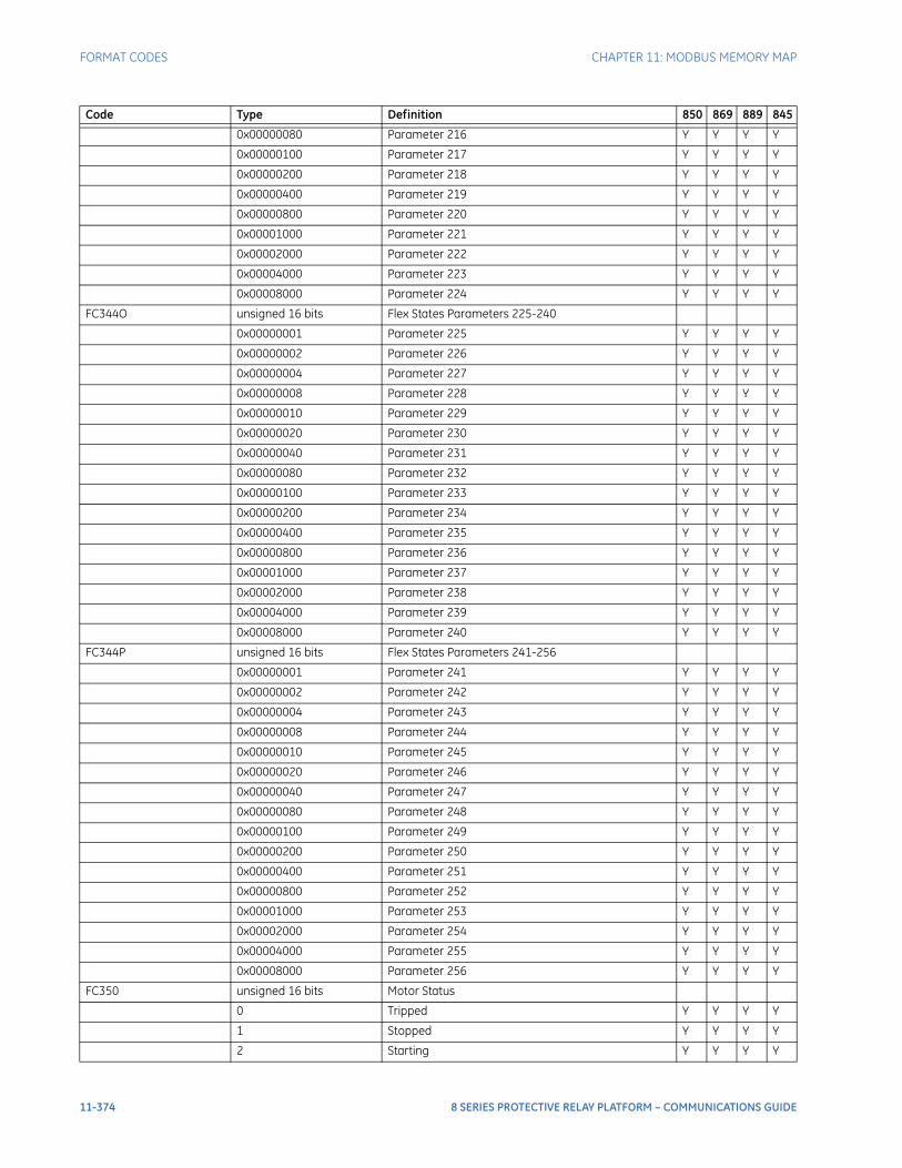
FORMAT CODES CHAPTER 11: MODBUS MEMORY MAP
0x00000080 Parameter 216 Y Y Y Y
0x00000100 Parameter 217 Y Y Y Y
0x00000200 Parameter 218 Y Y Y Y
0x00000400 Parameter 219 Y Y Y Y
0x00000800 Parameter 220 Y Y Y Y
0x00001000 Parameter 221 Y Y Y Y
0x00002000 Parameter 222 Y Y Y Y
0x00004000 Parameter 223 Y Y Y Y
0x00008000 Parameter 224 Y Y Y Y
FC344O unsigned 16 bits Flex States Parameters 225-240
0x00000001 Parameter 225 Y Y Y Y
0x00000002 Parameter 226 Y Y Y Y
0x00000004 Parameter 227 Y Y Y Y
0x00000008 Parameter 228 Y Y Y Y
0x00000010 Parameter 229 Y Y Y Y
0x00000020 Parameter 230 Y Y Y Y
0x00000040 Parameter 231 Y Y Y Y
0x00000080 Parameter 232 Y Y Y Y
0x00000100 Parameter 233 Y Y Y Y
0x00000200 Parameter 234 Y Y Y Y
0x00000400 Parameter 235 Y Y Y Y
0x00000800 Parameter 236 Y Y Y Y
0x00001000 Parameter 237 Y Y Y Y
0x00002000 Parameter 238 Y Y Y Y
0x00004000 Parameter 239 Y Y Y Y
0x00008000 Parameter 240 Y Y Y Y
FC344P unsigned 16 bits Flex States Parameters 241-256
0x00000001 Parameter 241 Y Y Y Y
0x00000002 Parameter 242 Y Y Y Y
0x00000004 Parameter 243 Y Y Y Y
0x00000008 Parameter 244 Y Y Y Y
0x00000010 Parameter 245 Y Y Y Y
0x00000020 Parameter 246 Y Y Y Y
0x00000040 Parameter 247 Y Y Y Y
0x00000080 Parameter 248 Y Y Y Y
0x00000100 Parameter 249 Y Y Y Y
0x00000200 Parameter 250 Y Y Y Y
0x00000400 Parameter 251 Y Y Y Y
0x00000800 Parameter 252 Y Y Y Y
0x00001000 Parameter 253 Y Y Y Y
0x00002000 Parameter 254 Y Y Y Y
0x00004000 Parameter 255 Y Y Y Y
0x00008000 Parameter 256 Y Y Y Y
FC350 unsigned 16 bits Motor Status
0 Tripped Y Y Y Y
1 Stopped Y Y Y Y
2 Starting Y Y Y Y
Code Type Definition 850 869 889 845
11-374 8 SERIES PROTECTIVE RELAY PLATFORM – COMMUNICATIONS GUIDE
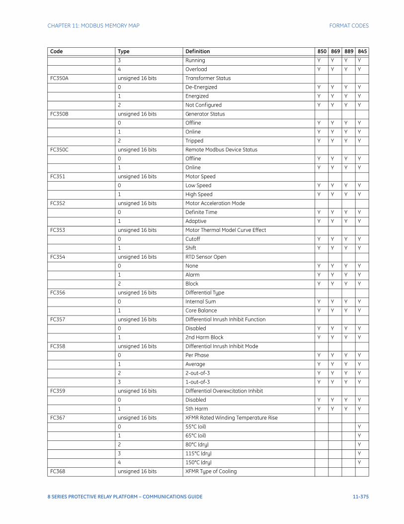
CHAPTER 11: MODBUS MEMORY MAP FORMAT CODES
3 Running Y Y Y Y
4 Overload Y Y Y Y
FC350A unsigned 16 bits Transformer Status
0 De-Energized Y Y Y Y
1 Energized Y Y Y Y
2 Not Configured Y Y Y Y
FC350B unsigned 16 bits Generator Status
0 Offline Y Y Y Y
1 Online Y Y Y Y
2 Tripped Y Y Y Y
FC350C unsigned 16 bits Remote Modbus Device Status
0 Offline Y Y Y Y
1 Online Y Y Y Y
FC351 unsigned 16 bits Motor Speed
0 Low Speed Y Y Y Y
1 High Speed Y Y Y Y
FC352 unsigned 16 bits Motor Acceleration Mode
0 Definite Time Y Y Y Y
1 Adaptive Y Y Y Y
FC353 unsigned 16 bits Motor Thermal Model Curve Effect
0 Cutoff Y Y Y Y
1 Shift Y Y Y Y
FC354 unsigned 16 bits RTD Sensor Open
0 None Y Y Y Y
1 Alarm Y Y Y Y
2 Block Y Y Y Y
FC356 unsigned 16 bits Differential Type
0 Internal Sum Y Y Y Y
1 Core Balance Y Y Y Y
FC357 unsigned 16 bits Differential Inrush Inhibit Function
0 Disabled Y Y Y Y
1 2nd Harm Block Y Y Y Y
FC358 unsigned 16 bits Differential Inrush Inhibit Mode
0 Per Phase Y Y Y Y
1 Average Y Y Y Y
2 2-out-of-3 Y Y Y Y
3 1-out-of-3 Y Y Y Y
FC359 unsigned 16 bits Differential Overexcitation Inhibit
0 Disabled Y Y Y Y
1 5th Harm Y Y Y Y
FC367 unsigned 16 bits XFMR Rated Winding Temperature Rise
0 55°C (oil) Y
1 65°C (oil) Y
2 80°C (dry) Y
3 115°C (dry) Y
4 150°C (dry) Y
FC368 unsigned 16 bits XFMR Type of Cooling
Code Type Definition 850 869 889 845
8 SERIES PROTECTIVE RELAY PLATFORM – COMMUNICATIONS GUIDE 11-375
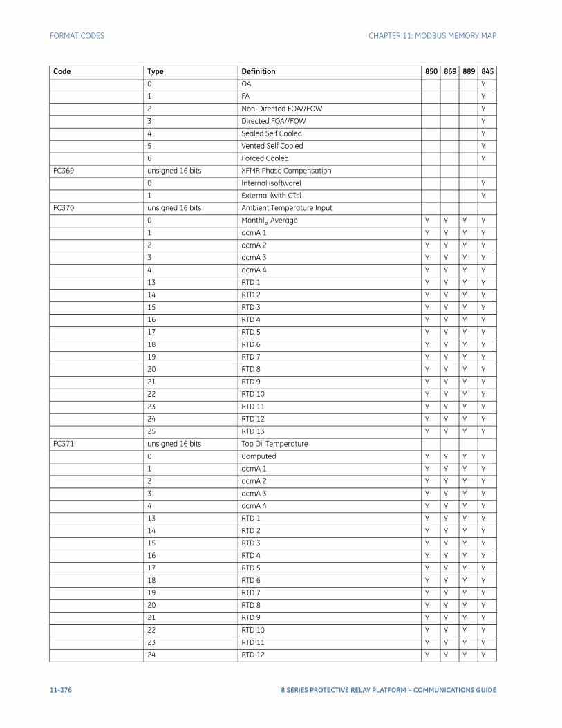
FORMAT CODES CHAPTER 11: MODBUS MEMORY MAP
0 OA Y
1 FA Y
2 Non-Directed FOA//FOW Y
3 Directed FOA//FOW Y
4 Sealed Self Cooled Y
5 Vented Self Cooled Y
6 Forced Cooled Y
FC369 unsigned 16 bits XFMR Phase Compensation
0 Internal (software) Y
1 External (with CTs) Y
FC370 unsigned 16 bits Ambient Temperature Input
0 Monthly Average Y Y Y Y
1 dcmA 1 Y Y Y Y
2 dcmA 2 Y Y Y Y
3 dcmA 3 Y Y Y Y
4 dcmA 4 Y Y Y Y
13 RTD 1 Y Y Y Y
14 RTD 2 Y Y Y Y
15 RTD 3 Y Y Y Y
16 RTD 4 Y Y Y Y
17 RTD 5 Y Y Y Y
18 RTD 6 Y Y Y Y
19 RTD 7 Y Y Y Y
20 RTD 8 Y Y Y Y
21 RTD 9 Y Y Y Y
22 RTD 10 Y Y Y Y
23 RTD 11 Y Y Y Y
24 RTD 12 Y Y Y Y
25 RTD 13 Y Y Y Y
FC371 unsigned 16 bits Top Oil Temperature
0 Computed Y Y Y Y
1 dcmA 1 Y Y Y Y
2 dcmA 2 Y Y Y Y
3 dcmA 3 Y Y Y Y
4 dcmA 4 Y Y Y Y
13 RTD 1 Y Y Y Y
14 RTD 2 Y Y Y Y
15 RTD 3 Y Y Y Y
16 RTD 4 Y Y Y Y
17 RTD 5 Y Y Y Y
18 RTD 6 Y Y Y Y
19 RTD 7 Y Y Y Y
20 RTD 8 Y Y Y Y
21 RTD 9 Y Y Y Y
22 RTD 10 Y Y Y Y
23 RTD 11 Y Y Y Y
24 RTD 12 Y Y Y Y
Code Type Definition 850 869 889 845
11-376 8 SERIES PROTECTIVE RELAY PLATFORM – COMMUNICATIONS GUIDE
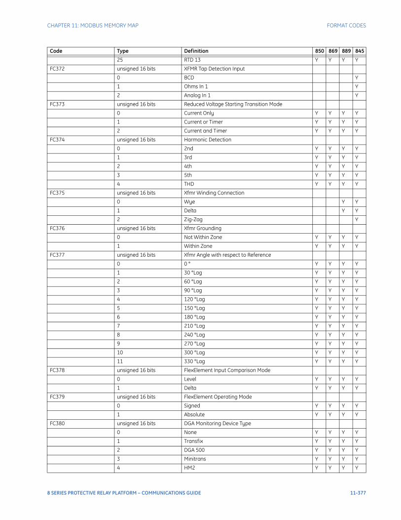
CHAPTER 11: MODBUS MEMORY MAP FORMAT CODES
25 RTD 13 Y Y Y Y
FC372 unsigned 16 bits XFMR Tap Detection Input
0 BCD Y
1 Ohms In 1 Y
2 Analog In 1 Y
FC373 unsigned 16 bits Reduced Voltage Starting Transition Mode
0 Current Only Y Y Y Y
1 Current or Timer Y Y Y Y
2 Current and Timer Y Y Y Y
FC374 unsigned 16 bits Harmonic Detection
0 2nd Y Y Y Y
1 3rd Y Y Y Y
2 4th Y Y Y Y
3 5th Y Y Y Y
4 THD Y Y Y Y
FC375 unsigned 16 bits Xfmr Winding Connection
0 Wye Y Y
1 Delta Y Y
2 Zig-Zag Y
FC376 unsigned 16 bits Xfmr Grounding
0 Not Within Zone Y Y Y Y
1 Within Zone Y Y Y Y
FC377 unsigned 16 bits Xfmr Angle with respect to Reference
0 0 ° Y Y Y Y
1 30 °Lag Y Y Y Y
2 60 °Lag Y Y Y Y
3 90 °Lag Y Y Y Y
4 120 °Lag Y Y Y Y
5 150 °Lag Y Y Y Y
6 180 °Lag Y Y Y Y
7 210 °Lag Y Y Y Y
8 240 °Lag Y Y Y Y
9 270 °Lag Y Y Y Y
10 300 °Lag Y Y Y Y
11 330 °Lag Y Y Y Y
FC378 unsigned 16 bits FlexElement Input Comparison Mode
0 Level Y Y Y Y
1 Delta Y Y Y Y
FC379 unsigned 16 bits FlexElement Operating Mode
0 Signed Y Y Y Y
1 Absolute Y Y Y Y
FC380 unsigned 16 bits DGA Monitoring Device Type
0 None Y Y Y Y
1 Transfix Y Y Y Y
2 DGA 500 Y Y Y Y
3 Minitrans Y Y Y Y
4 HM2 Y Y Y Y
Code Type Definition 850 869 889 845
8 SERIES PROTECTIVE RELAY PLATFORM – COMMUNICATIONS GUIDE 11-377
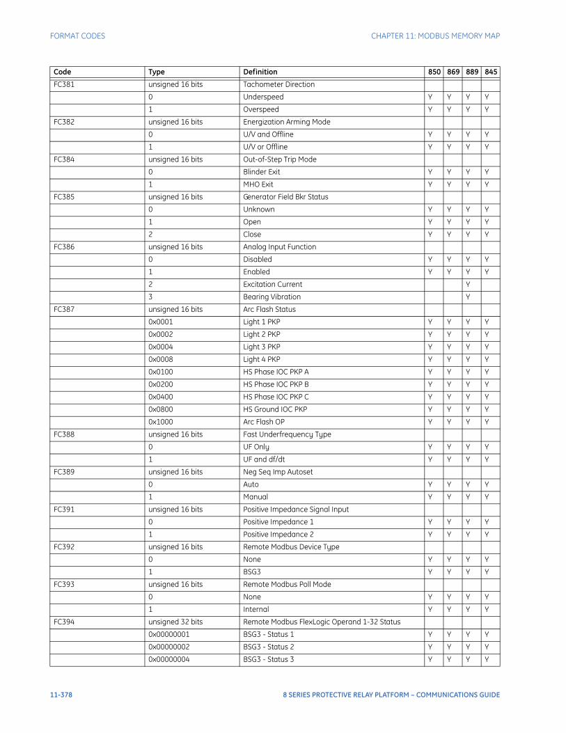
FORMAT CODES CHAPTER 11: MODBUS MEMORY MAP
FC381 unsigned 16 bits Tachometer Direction
0 Underspeed Y Y Y Y
1 Overspeed Y Y Y Y
FC382 unsigned 16 bits Energization Arming Mode
0 U/V and Offline Y Y Y Y
1 U/V or Offline Y Y Y Y
FC384 unsigned 16 bits Out-of-Step Trip Mode
0 Blinder Exit Y Y Y Y
1 MHO Exit Y Y Y Y
FC385 unsigned 16 bits Generator Field Bkr Status
0 Unknown Y Y Y Y
1 Open Y Y Y Y
2 Close Y Y Y Y
FC386 unsigned 16 bits Analog Input Function
0 Disabled Y Y Y Y
1 Enabled Y Y Y Y
2 Excitation Current Y
3 Bearing Vibration Y
FC387 unsigned 16 bits Arc Flash Status
0x0001 Light 1 PKP Y Y Y Y
0x0002 Light 2 PKP Y Y Y Y
0x0004 Light 3 PKP Y Y Y Y
0x0008 Light 4 PKP Y Y Y Y
0x0100 HS Phase IOC PKP A Y Y Y Y
0x0200 HS Phase IOC PKP B Y Y Y Y
0x0400 HS Phase IOC PKP C Y Y Y Y
0x0800 HS Ground IOC PKP Y Y Y Y
0x1000 Arc Flash OP Y Y Y Y
FC388 unsigned 16 bits Fast Underfrequency Type
0 UF Only Y Y Y Y
1 UF and df/dt Y Y Y Y
FC389 unsigned 16 bits Neg Seq Imp Autoset
0 Auto Y Y Y Y
1 Manual Y Y Y Y
FC391 unsigned 16 bits Positive Impedance Signal Input
0 Positive Impedance 1 Y Y Y Y
1 Positive Impedance 2 Y Y Y Y
FC392 unsigned 16 bits Remote Modbus Device Type
0 None Y Y Y Y
1 BSG3 Y Y Y Y
FC393 unsigned 16 bits Remote Modbus Poll Mode
0 None Y Y Y Y
1 Internal Y Y Y Y
FC394 unsigned 32 bits Remote Modbus FlexLogic Operand 1-32 Status
0x00000001 BSG3 - Status 1 Y Y Y Y
0x00000002 BSG3 - Status 2 Y Y Y Y
0x00000004 BSG3 - Status 3 Y Y Y Y
Code Type Definition 850 869 889 845
11-378 8 SERIES PROTECTIVE RELAY PLATFORM – COMMUNICATIONS GUIDE
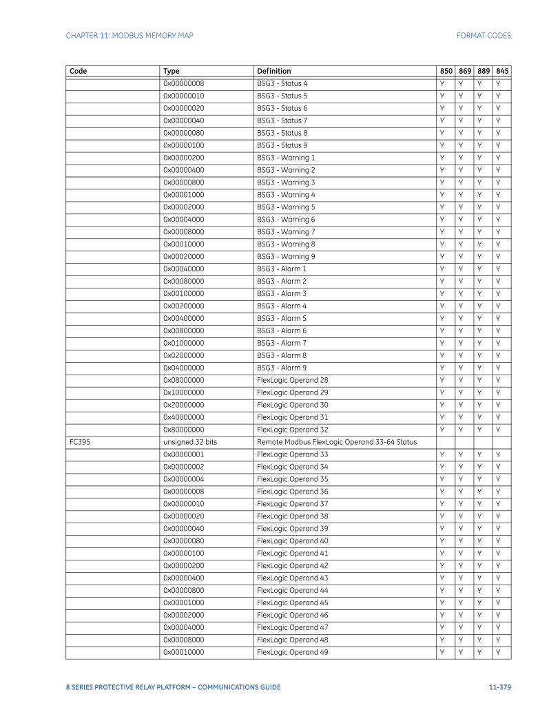
CHAPTER 11: MODBUS MEMORY MAP FORMAT CODES
0x00000008 BSG3 - Status 4 Y Y Y Y
0x00000010 BSG3 - Status 5 Y Y Y Y
0x00000020 BSG3 - Status 6 Y Y Y Y
0x00000040 BSG3 - Status 7 Y Y Y Y
0x00000080 BSG3 - Status 8 Y Y Y Y
0x00000100 BSG3 - Status 9 Y Y Y Y
0x00000200 BSG3 - Warning 1 Y Y Y Y
0x00000400 BSG3 - Warning 2 Y Y Y Y
0x00000800 BSG3 - Warning 3 Y Y Y Y
0x00001000 BSG3 - Warning 4 Y Y Y Y
0x00002000 BSG3 - Warning 5 Y Y Y Y
0x00004000 BSG3 - Warning 6 Y Y Y Y
0x00008000 BSG3 - Warning 7 Y Y Y Y
0x00010000 BSG3 - Warning 8 Y Y Y Y
0x00020000 BSG3 - Warning 9 Y Y Y Y
0x00040000 BSG3 - Alarm 1 Y Y Y Y
0x00080000 BSG3 - Alarm 2 Y Y Y Y
0x00100000 BSG3 - Alarm 3 Y Y Y Y
0x00200000 BSG3 - Alarm 4 Y Y Y Y
0x00400000 BSG3 - Alarm 5 Y Y Y Y
0x00800000 BSG3 - Alarm 6 Y Y Y Y
0x01000000 BSG3 - Alarm 7 Y Y Y Y
0x02000000 BSG3 - Alarm 8 Y Y Y Y
0x04000000 BSG3 - Alarm 9 Y Y Y Y
0x08000000 FlexLogic Operand 28 Y Y Y Y
0x10000000 FlexLogic Operand 29 Y Y Y Y
0x20000000 FlexLogic Operand 30 Y Y Y Y
0x40000000 FlexLogic Operand 31 Y Y Y Y
0x80000000 FlexLogic Operand 32 Y Y Y Y
FC395 unsigned 32 bits Remote Modbus FlexLogic Operand 33-64 Status
0x00000001 FlexLogic Operand 33 Y Y Y Y
0x00000002 FlexLogic Operand 34 Y Y Y Y
0x00000004 FlexLogic Operand 35 Y Y Y Y
0x00000008 FlexLogic Operand 36 Y Y Y Y
0x00000010 FlexLogic Operand 37 Y Y Y Y
0x00000020 FlexLogic Operand 38 Y Y Y Y
0x00000040 FlexLogic Operand 39 Y Y Y Y
0x00000080 FlexLogic Operand 40 Y Y Y Y
0x00000100 FlexLogic Operand 41 Y Y Y Y
0x00000200 FlexLogic Operand 42 Y Y Y Y
0x00000400 FlexLogic Operand 43 Y Y Y Y
0x00000800 FlexLogic Operand 44 Y Y Y Y
0x00001000 FlexLogic Operand 45 Y Y Y Y
0x00002000 FlexLogic Operand 46 Y Y Y Y
0x00004000 FlexLogic Operand 47 Y Y Y Y
0x00008000 FlexLogic Operand 48 Y Y Y Y
0x00010000 FlexLogic Operand 49 Y Y Y Y
Code Type Definition 850 869 889 845
8 SERIES PROTECTIVE RELAY PLATFORM – COMMUNICATIONS GUIDE 11-379
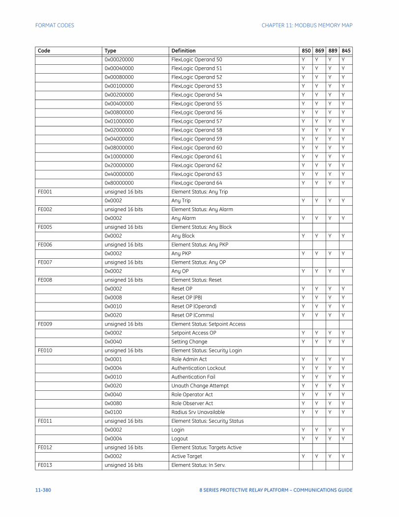
FORMAT CODES CHAPTER 11: MODBUS MEMORY MAP
0x00020000 FlexLogic Operand 50 Y Y Y Y
0x00040000 FlexLogic Operand 51 Y Y Y Y
0x00080000 FlexLogic Operand 52 Y Y Y Y
0x00100000 FlexLogic Operand 53 Y Y Y Y
0x00200000 FlexLogic Operand 54 Y Y Y Y
0x00400000 FlexLogic Operand 55 Y Y Y Y
0x00800000 FlexLogic Operand 56 Y Y Y Y
0x01000000 FlexLogic Operand 57 Y Y Y Y
0x02000000 FlexLogic Operand 58 Y Y Y Y
0x04000000 FlexLogic Operand 59 Y Y Y Y
0x08000000 FlexLogic Operand 60 Y Y Y Y
0x10000000 FlexLogic Operand 61 Y Y Y Y
0x20000000 FlexLogic Operand 62 Y Y Y Y
0x40000000 FlexLogic Operand 63 Y Y Y Y
0x80000000 FlexLogic Operand 64 Y Y Y Y
FE001 unsigned 16 bits Element Status: Any Trip
0x0002 Any Trip Y Y Y Y
FE002 unsigned 16 bits Element Status: Any Alarm
0x0002 Any Alarm Y Y Y Y
FE005 unsigned 16 bits Element Status: Any Block
0x0002 Any Block Y Y Y Y
FE006 unsigned 16 bits Element Status: Any PKP
0x0002 Any PKP Y Y Y Y
FE007 unsigned 16 bits Element Status: Any OP
0x0002 Any OP Y Y Y Y
FE008 unsigned 16 bits Element Status: Reset
0x0002 Reset OP Y Y Y Y
0x0008 Reset OP (PB) Y Y Y Y
0x0010 Reset OP (Operand) Y Y Y Y
0x0020 Reset OP (Comms) Y Y Y Y
FE009 unsigned 16 bits Element Status: Setpoint Access
0x0002 Setpoint Access OP Y Y Y Y
0x0040 Setting Change Y Y Y Y
FE010 unsigned 16 bits Element Status: Security Login
0x0001 Role Admin Act Y Y Y Y
0x0004 Authentication Lockout Y Y Y Y
0x0010 Authentication Fail Y Y Y Y
0x0020 Unauth Change Attempt Y Y Y Y
0x0040 Role Operator Act Y Y Y Y
0x0080 Role Observer Act Y Y Y Y
0x0100 Radius Srv Unavailable Y Y Y Y
FE011 unsigned 16 bits Element Status: Security Status
0x0002 Login Y Y Y Y
0x0004 Logout Y Y Y Y
FE012 unsigned 16 bits Element Status: Targets Active
0x0002 Active Target Y Y Y Y
FE013 unsigned 16 bits Element Status: In Serv.
Code Type Definition 850 869 889 845
11-380 8 SERIES PROTECTIVE RELAY PLATFORM – COMMUNICATIONS GUIDE
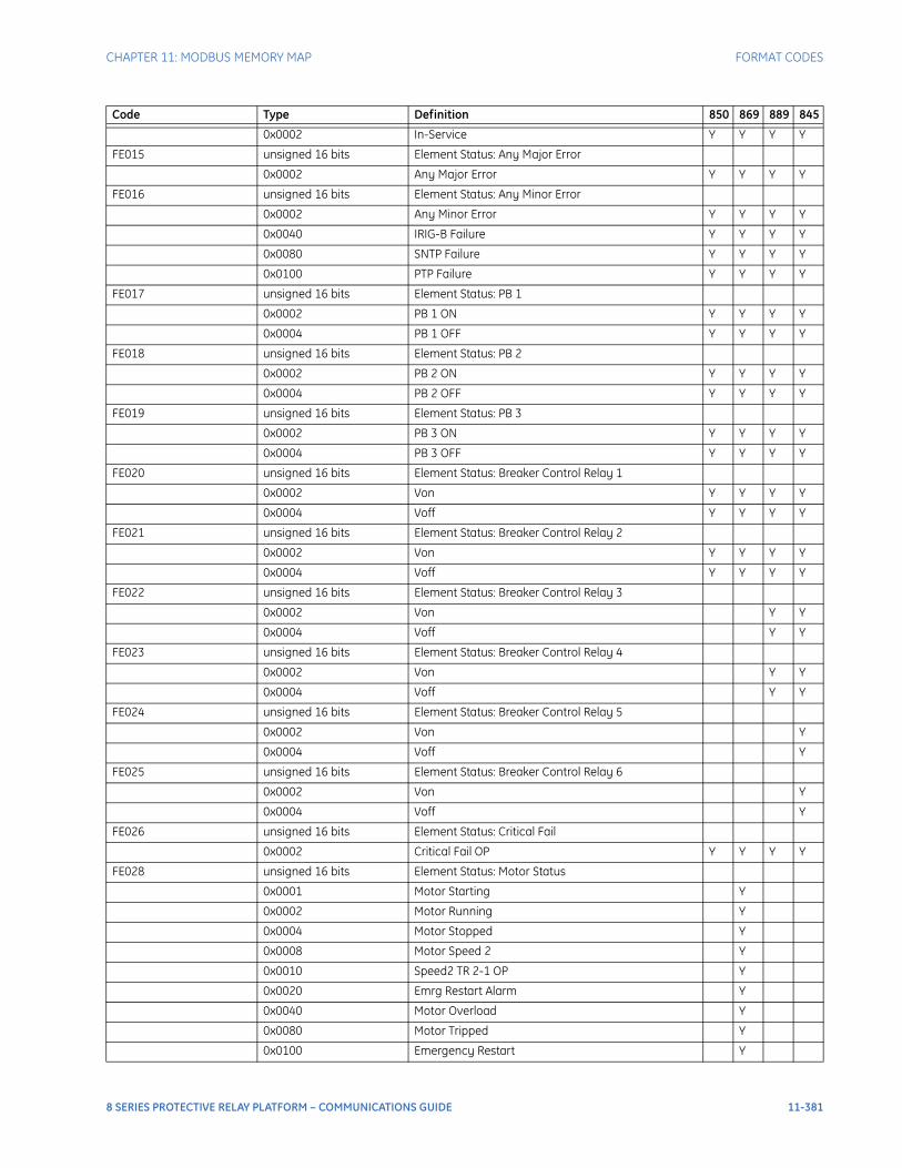
CHAPTER 11: MODBUS MEMORY MAP FORMAT CODES
0x0002 In-Service Y Y Y Y
FE015 unsigned 16 bits Element Status: Any Major Error
0x0002 Any Major Error Y Y Y Y
FE016 unsigned 16 bits Element Status: Any Minor Error
0x0002 Any Minor Error Y Y Y Y
0x0040 IRIG-B Failure Y Y Y Y
0x0080 SNTP Failure Y Y Y Y
0x0100 PTP Failure Y Y Y Y
FE017 unsigned 16 bits Element Status: PB 1
0x0002 PB 1 ON Y Y Y Y
0x0004 PB 1 OFF Y Y Y Y
FE018 unsigned 16 bits Element Status: PB 2
0x0002 PB 2 ON Y Y Y Y
0x0004 PB 2 OFF Y Y Y Y
FE019 unsigned 16 bits Element Status: PB 3
0x0002 PB 3 ON Y Y Y Y
0x0004 PB 3 OFF Y Y Y Y
FE020 unsigned 16 bits Element Status: Breaker Control Relay 1
0x0002 Von Y Y Y Y
0x0004 Voff Y Y Y Y
FE021 unsigned 16 bits Element Status: Breaker Control Relay 2
0x0002 Von Y Y Y Y
0x0004 Voff Y Y Y Y
FE022 unsigned 16 bits Element Status: Breaker Control Relay 3
0x0002 Von Y Y
0x0004 Voff Y Y
FE023 unsigned 16 bits Element Status: Breaker Control Relay 4
0x0002 Von Y Y
0x0004 Voff Y Y
FE024 unsigned 16 bits Element Status: Breaker Control Relay 5
0x0002 Von Y
0x0004 Voff Y
FE025 unsigned 16 bits Element Status: Breaker Control Relay 6
0x0002 Von Y
0x0004 Voff Y
FE026 unsigned 16 bits Element Status: Critical Fail
0x0002 Critical Fail OP Y Y Y Y
FE028 unsigned 16 bits Element Status: Motor Status
0x0001 Motor Starting Y
0x0002 Motor Running Y
0x0004 Motor Stopped Y
0x0008 Motor Speed 2 Y
0x0010 Speed2 TR 2-1 OP Y
0x0020 Emrg Restart Alarm Y
0x0040 Motor Overload Y
0x0080 Motor Tripped Y
0x0100 Emergency Restart Y
Code Type Definition 850 869 889 845
8 SERIES PROTECTIVE RELAY PLATFORM – COMMUNICATIONS GUIDE 11-381

FORMAT CODES CHAPTER 11: MODBUS MEMORY MAP
FE029 unsigned 16 bits Element Status: BKR1 Status Closed
0x0002 BKR1 Closed Y Y Y Y
FE030 unsigned 16 bits Element Status: BKR1 Status Opened
0x0002 BKR1 Opened Y Y Y Y
FE031 unsigned 16 bits Element Status: BKR1 Status Unknown
0x0002 BKR1 Unkwn State Y Y Y Y
0x0004 BKR1 Not Config Y Y Y Y
FE032 unsigned 16 bits Element Status: BKR1 Status Disconnected
0x0002 BKR1 Disconnected Y Y Y Y
0x0004 BKR1 Connected Y Y Y Y
FE033 unsigned 16 bits Element Status: BKR1 52a Contact
0x0002 BKR1 52a CI ON Y Y Y Y
0x0004 BKR1 52a CI OFF Y Y Y Y
FE034 unsigned 16 bits Element Status: BKR1 52b Contact
0x0002 BKR1 52b CI ON Y Y Y Y
0x0004 BKR1 52b CI OFF Y Y Y Y
FE035 unsigned 16 bits Element Status: BKR2 Status Closed
0x0002 BKR2 Closed Y Y
FE036 unsigned 16 bits Element Status: BKR2 Status Opened
0x0002 BKR2 Opened Y Y
FE037 unsigned 16 bits Element Status: BKR2 Status Unknown
0x0002 BKR2 Unkwn State Y Y
0x0004 BKR2 Not Config Y Y
FE038 unsigned 16 bits Element Status: BKR2 Status Disconnected
0x0002 BKR2 Disconnected Y Y
0x0004 BKR2 Connected Y Y
FE039 unsigned 16 bits Element Status: BKR2 52a Contact
0x0002 BKR2 52a CI ON Y Y
0x0004 BKR2 52a CI OFF Y Y
FE040 unsigned 16 bits Element Status: BKR2 52b Contact
0x0002 BKR2 52b CI ON Y Y
0x0004 BKR2 52b CI OFF Y Y
FE041 unsigned 16 bits Element Status: BKR3 Status Closed
0x0002 BKR3 Closed Y
FE042 unsigned 16 bits Element Status: BKR3 Status Opened
0x0002 BKR3 Opened Y
FE043 unsigned 16 bits Element Status: BKR3 Status Unknown
0x0002 BKR3 Unkwn State Y
0x0004 BKR3 Not Config Y
FE044 unsigned 16 bits Element Status: BKR3 Status Disconnected
0x0002 BKR3 Disconnected Y
0x0004 BKR3 Connected Y
FE045 unsigned 16 bits Element Status: BKR3 52a Contact
0x0002 BKR3 52a CI ON Y
0x0004 BKR3 52a CI OFF Y
FE046 unsigned 16 bits Element Status: BKR3 52b Contact
0x0002 BKR3 52b CI ON Y
Code Type Definition 850 869 889 845
11-382 8 SERIES PROTECTIVE RELAY PLATFORM – COMMUNICATIONS GUIDE
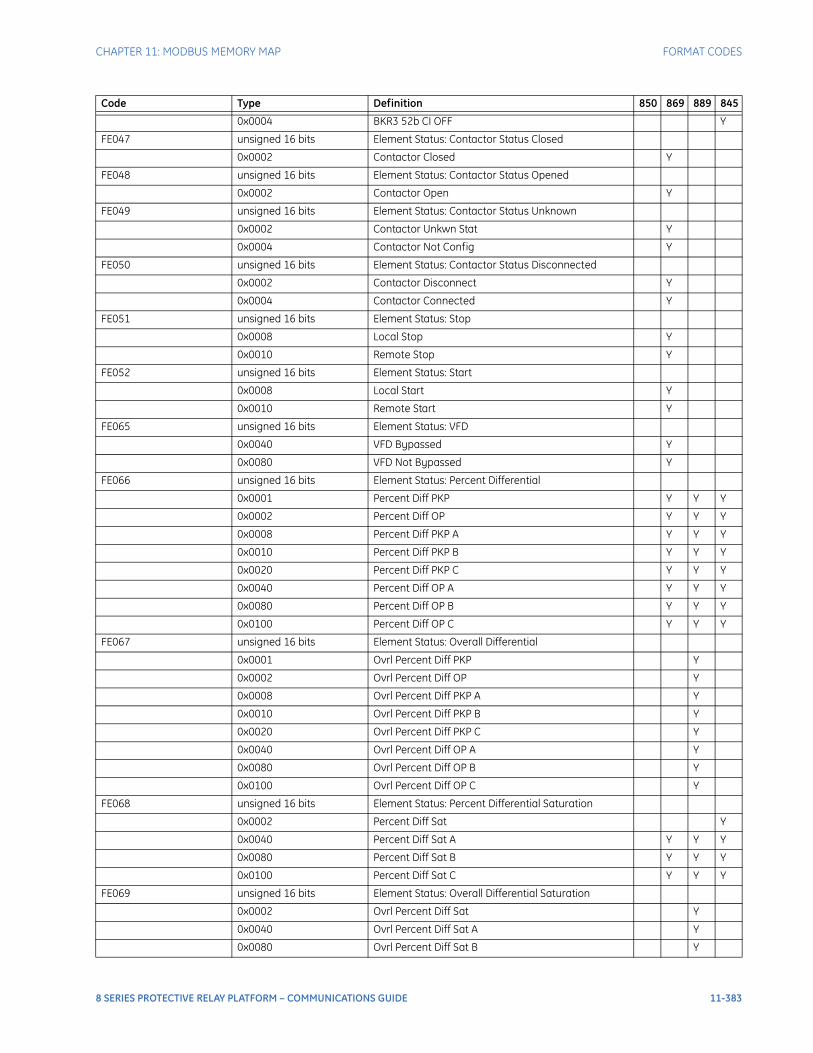
CHAPTER 11: MODBUS MEMORY MAP FORMAT CODES
0x0004 BKR3 52b CI OFF Y
FE047 unsigned 16 bits Element Status: Contactor Status Closed
0x0002 Contactor Closed Y
FE048 unsigned 16 bits Element Status: Contactor Status Opened
0x0002 Contactor Open Y
FE049 unsigned 16 bits Element Status: Contactor Status Unknown
0x0002 Contactor Unkwn Stat Y
0x0004 Contactor Not Config Y
FE050 unsigned 16 bits Element Status: Contactor Status Disconnected
0x0002 Contactor Disconnect Y
0x0004 Contactor Connected Y
FE051 unsigned 16 bits Element Status: Stop
0x0008 Local Stop Y
0x0010 Remote Stop Y
FE052 unsigned 16 bits Element Status: Start
0x0008 Local Start Y
0x0010 Remote Start Y
FE065 unsigned 16 bits Element Status: VFD
0x0040 VFD Bypassed Y
0x0080 VFD Not Bypassed Y
FE066 unsigned 16 bits Element Status: Percent Differential
0x0001 Percent Diff PKP Y Y Y
0x0002 Percent Diff OP Y Y Y
0x0008 Percent Diff PKP A Y Y Y
0x0010 Percent Diff PKP B Y Y Y
0x0020 Percent Diff PKP C Y Y Y
0x0040 Percent Diff OP A Y Y Y
0x0080 Percent Diff OP B Y Y Y
0x0100 Percent Diff OP C Y Y Y
FE067 unsigned 16 bits Element Status: Overall Differential
0x0001 Ovrl Percent Diff PKP Y
0x0002 Ovrl Percent Diff OP Y
0x0008 Ovrl Percent Diff PKP A Y
0x0010 Ovrl Percent Diff PKP B Y
0x0020 Ovrl Percent Diff PKP C Y
0x0040 Ovrl Percent Diff OP A Y
0x0080 Ovrl Percent Diff OP B Y
0x0100 Ovrl Percent Diff OP C Y
FE068 unsigned 16 bits Element Status: Percent Differential Saturation
0x0002 Percent Diff Sat Y
0x0040 Percent Diff Sat A Y Y Y
0x0080 Percent Diff Sat B Y Y Y
0x0100 Percent Diff Sat C Y Y Y
FE069 unsigned 16 bits Element Status: Overall Differential Saturation
0x0002 Ovrl Percent Diff Sat Y
0x0040 Ovrl Percent Diff Sat A Y
0x0080 Ovrl Percent Diff Sat B Y
Code Type Definition 850 869 889 845
8 SERIES PROTECTIVE RELAY PLATFORM – COMMUNICATIONS GUIDE 11-383

FORMAT CODES CHAPTER 11: MODBUS MEMORY MAP
0x0100 Ovrl Percent Diff Sat C Y
FE070 unsigned 16 bits Element Status: Percent Differential Direction
0x0002 Percent Diff Dir Y
0x0040 Percent Diff Dir A Y Y Y
0x0080 Percent Diff Dir B Y Y Y
0x0100 Percent Diff Dir C Y Y Y
FE071 unsigned 16 bits Element Status: Overall Differential Direction
0x0002 Ovrl Percent Diff Dir Y
0x0040 Ovrl Percent Diff Dir A Y
0x0080 Ovrl Percent Diff Dir B Y
0x0100 Ovrl Percent Diff Dir C Y
FE072 unsigned 16 bits Element Status: Percent Differential Warning
0x0002 Percent Diff Warn Y Y Y
FE073 unsigned 16 bits Element Status: Overall Differential Warning
0x0002 Ovrl Percent Diff Warn Y
FE074 unsigned 16 bits Element Status: Percent Differential Harmonic
0x0002 Percent Diff Blocked Y
0x0008 2nd Harm Diff A Y
0x0010 2nd Harm Diff B Y
0x0020 2nd Harm Diff C Y
0x0040 5th Harm Diff A Y
0x0080 5th Harm Diff B Y
0x0100 5th Harm Diff C Y
FE075 unsigned 16 bits Element Status: Overall Differential Harmonic
0x0002 Ovrl Percent Diff Blocked Y
0x0008 2nd Harm Diff A Y
0x0010 2nd Harm Diff B Y
0x0020 2nd Harm Diff C Y
0x0040 5th Harm Diff A Y
0x0080 5th Harm Diff B Y
0x0100 5th Harm Diff C Y
FE076 unsigned 16 bits Element Status: Instantaneous Differential
0x0002 Instant Diff OP Y
0x0040 Instant Diff OP A Y
0x0080 Instant Diff OP B Y
0x0100 Instant Diff OP C Y
FE077 unsigned 16 bits Element Status: Overall Instantaneous Differential
0x0002 Instant Diff OP Y
0x0040 Instant Diff OP A Y
0x0080 Instant Diff OP B Y
0x0100 Instant Diff OP C Y
FE078 unsigned 16 bits Element Status: Thermal Trip
0x0001 Thermal PKP Y
0x0002 Thermal OP Y
FE079 unsigned 16 bits Element Status: Thermal Alarm
0x0002 Thermal Alarm OP Y
FE080 unsigned 16 bits Element Status: Current Unbalance Alarm
Code Type Definition 850 869 889 845
11-384 8 SERIES PROTECTIVE RELAY PLATFORM – COMMUNICATIONS GUIDE
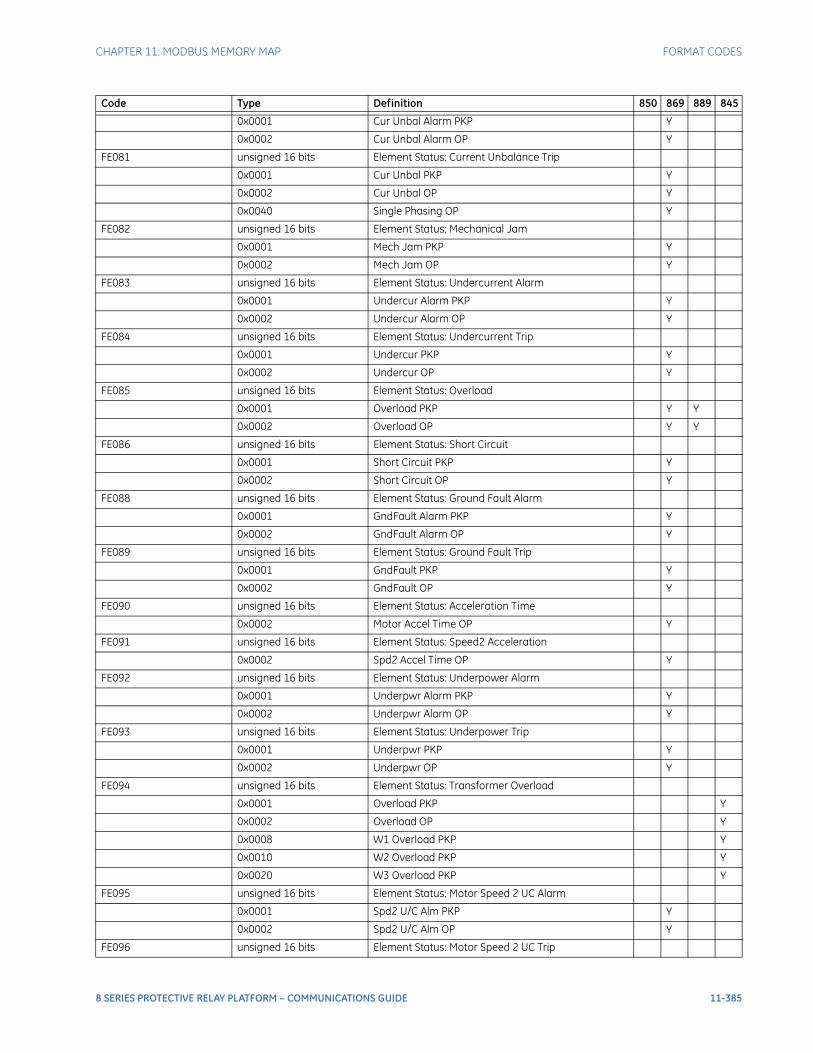
CHAPTER 11: MODBUS MEMORY MAP FORMAT CODES
0x0001 Cur Unbal Alarm PKP Y
0x0002 Cur Unbal Alarm OP Y
FE081 unsigned 16 bits Element Status: Current Unbalance Trip
0x0001 Cur Unbal PKP Y
0x0002 Cur Unbal OP Y
0x0040 Single Phasing OP Y
FE082 unsigned 16 bits Element Status: Mechanical Jam
0x0001 Mech Jam PKP Y
0x0002 Mech Jam OP Y
FE083 unsigned 16 bits Element Status: Undercurrent Alarm
0x0001 Undercur Alarm PKP Y
0x0002 Undercur Alarm OP Y
FE084 unsigned 16 bits Element Status: Undercurrent Trip
0x0001 Undercur PKP Y
0x0002 Undercur OP Y
FE085 unsigned 16 bits Element Status: Overload
0x0001 Overload PKP Y Y
0x0002 Overload OP Y Y
FE086 unsigned 16 bits Element Status: Short Circuit
0x0001 Short Circuit PKP Y
0x0002 Short Circuit OP Y
FE088 unsigned 16 bits Element Status: Ground Fault Alarm
0x0001 GndFault Alarm PKP Y
0x0002 GndFault Alarm OP Y
FE089 unsigned 16 bits Element Status: Ground Fault Trip
0x0001 GndFault PKP Y
0x0002 GndFault OP Y
FE090 unsigned 16 bits Element Status: Acceleration Time
0x0002 Motor Accel Time OP Y
FE091 unsigned 16 bits Element Status: Speed2 Acceleration
0x0002 Spd2 Accel Time OP Y
FE092 unsigned 16 bits Element Status: Underpower Alarm
0x0001 Underpwr Alarm PKP Y
0x0002 Underpwr Alarm OP Y
FE093 unsigned 16 bits Element Status: Underpower Trip
0x0001 Underpwr PKP Y
0x0002 Underpwr OP Y
FE094 unsigned 16 bits Element Status: Transformer Overload
0x0001 Overload PKP Y
0x0002 Overload OP Y
0x0008 W1 Overload PKP Y
0x0010 W2 Overload PKP Y
0x0020 W3 Overload PKP Y
FE095 unsigned 16 bits Element Status: Motor Speed 2 UC Alarm
0x0001 Spd2 U/C Alm PKP Y
0x0002 Spd2 U/C Alm OP Y
FE096 unsigned 16 bits Element Status: Motor Speed 2 UC Trip
Code Type Definition 850 869 889 845
8 SERIES PROTECTIVE RELAY PLATFORM – COMMUNICATIONS GUIDE 11-385
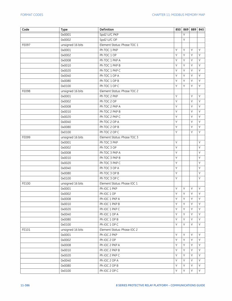
FORMAT CODES CHAPTER 11: MODBUS MEMORY MAP
0x0001 Spd2 U/C PKP Y
0x0002 Spd2 U/C OP Y
FE097 unsigned 16 bits Element Status: Phase TOC 1
0x0001 Ph TOC 1 PKP Y Y Y Y
0x0002 Ph TOC 1 OP Y Y Y Y
0x0008 Ph TOC 1 PKP A Y Y Y Y
0x0010 Ph TOC 1 PKP B Y Y Y Y
0x0020 Ph TOC 1 PKP C Y Y Y Y
0x0040 Ph TOC 1 OP A Y Y Y Y
0x0080 Ph TOC 1 OP B Y Y Y Y
0x0100 Ph TOC 1 OP C Y Y Y Y
FE098 unsigned 16 bits Element Status: Phase TOC 2
0x0001 Ph TOC 2 PKP Y Y Y
0x0002 Ph TOC 2 OP Y Y Y
0x0008 Ph TOC 2 PKP A Y Y Y
0x0010 Ph TOC 2 PKP B Y Y Y
0x0020 Ph TOC 2 PKP C Y Y Y
0x0040 Ph TOC 2 OP A Y Y Y
0x0080 Ph TOC 2 OP B Y Y Y
0x0100 Ph TOC 2 OP C Y Y Y
FE099 unsigned 16 bits Element Status: Phase TOC 3
0x0001 Ph TOC 3 PKP Y Y
0x0002 Ph TOC 3 OP Y Y
0x0008 Ph TOC 3 PKP A Y Y
0x0010 Ph TOC 3 PKP B Y Y
0x0020 Ph TOC 3 PKP C Y Y
0x0040 Ph TOC 3 OP A Y Y
0x0080 Ph TOC 3 OP B Y Y
0x0100 Ph TOC 3 OP C Y Y
FE100 unsigned 16 bits Element Status: Phase IOC 1
0x0001 Ph IOC 1 PKP Y Y Y Y
0x0002 Ph IOC 1 OP Y Y Y Y
0x0008 Ph IOC 1 PKP A Y Y Y Y
0x0010 Ph IOC 1 PKP B Y Y Y Y
0x0020 Ph IOC 1 PKP C Y Y Y Y
0x0040 Ph IOC 1 OP A Y Y Y Y
0x0080 Ph IOC 1 OP B Y Y Y Y
0x0100 Ph IOC 1 OP C Y Y Y Y
FE101 unsigned 16 bits Element Status: Phase IOC 2
0x0001 Ph IOC 2 PKP Y Y Y Y
0x0002 Ph IOC 2 OP Y Y Y Y
0x0008 Ph IOC 2 PKP A Y Y Y Y
0x0010 Ph IOC 2 PKP B Y Y Y Y
0x0020 Ph IOC 2 PKP C Y Y Y Y
0x0040 Ph IOC 2 OP A Y Y Y Y
0x0080 Ph IOC 2 OP B Y Y Y Y
0x0100 Ph IOC 2 OP C Y Y Y Y
Code Type Definition 850 869 889 845
11-386 8 SERIES PROTECTIVE RELAY PLATFORM – COMMUNICATIONS GUIDE
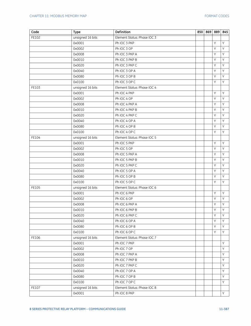
CHAPTER 11: MODBUS MEMORY MAP FORMAT CODES
FE102 unsigned 16 bits Element Status: Phase IOC 3
0x0001 Ph IOC 3 PKP Y Y
0x0002 Ph IOC 3 OP Y Y
0x0008 Ph IOC 3 PKP A Y Y
0x0010 Ph IOC 3 PKP B Y Y
0x0020 Ph IOC 3 PKP C Y Y
0x0040 Ph IOC 3 OP A Y Y
0x0080 Ph IOC 3 OP B Y Y
0x0100 Ph IOC 3 OP C Y Y
FE103 unsigned 16 bits Element Status: Phase IOC 4
0x0001 Ph IOC 4 PKP Y Y
0x0002 Ph IOC 4 OP Y Y
0x0008 Ph IOC 4 PKP A Y Y
0x0010 Ph IOC 4 PKP B Y Y
0x0020 Ph IOC 4 PKP C Y Y
0x0040 Ph IOC 4 OP A Y Y
0x0080 Ph IOC 4 OP B Y Y
0x0100 Ph IOC 4 OP C Y Y
FE104 unsigned 16 bits Element Status: Phase IOC 5
0x0001 Ph IOC 5 PKP Y Y
0x0002 Ph IOC 5 OP Y Y
0x0008 Ph IOC 5 PKP A Y Y
0x0010 Ph IOC 5 PKP B Y Y
0x0020 Ph IOC 5 PKP C Y Y
0x0040 Ph IOC 5 OP A Y Y
0x0080 Ph IOC 5 OP B Y Y
0x0100 Ph IOC 5 OP C Y Y
FE105 unsigned 16 bits Element Status: Phase IOC 6
0x0001 Ph IOC 6 PKP Y Y
0x0002 Ph IOC 6 OP Y Y
0x0008 Ph IOC 6 PKP A Y Y
0x0010 Ph IOC 6 PKP B Y Y
0x0020 Ph IOC 6 PKP C Y Y
0x0040 Ph IOC 6 OP A Y Y
0x0080 Ph IOC 6 OP B Y Y
0x0100 Ph IOC 6 OP C Y Y
FE106 unsigned 16 bits Element Status: Phase IOC 7
0x0001 Ph IOC 7 PKP Y
0x0002 Ph IOC 7 OP Y
0x0008 Ph IOC 7 PKP A Y
0x0010 Ph IOC 7 PKP B Y
0x0020 Ph IOC 7 PKP C Y
0x0040 Ph IOC 7 OP A Y
0x0080 Ph IOC 7 OP B Y
0x0100 Ph IOC 7 OP C Y
FE107 unsigned 16 bits Element Status: Phase IOC 8
0x0001 Ph IOC 8 PKP Y
Code Type Definition 850 869 889 845
8 SERIES PROTECTIVE RELAY PLATFORM – COMMUNICATIONS GUIDE 11-387
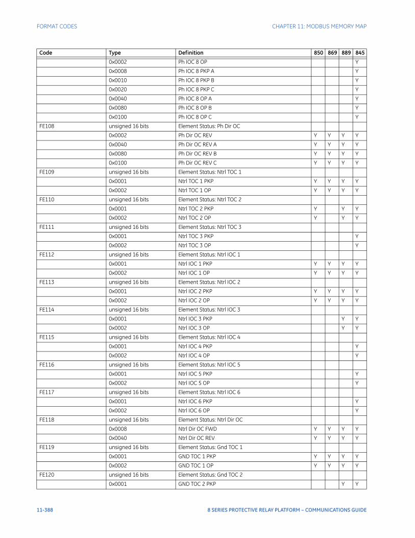
FORMAT CODES CHAPTER 11: MODBUS MEMORY MAP
0x0002 Ph IOC 8 OP Y
0x0008 Ph IOC 8 PKP A Y
0x0010 Ph IOC 8 PKP B Y
0x0020 Ph IOC 8 PKP C Y
0x0040 Ph IOC 8 OP A Y
0x0080 Ph IOC 8 OP B Y
0x0100 Ph IOC 8 OP C Y
FE108 unsigned 16 bits Element Status: Ph Dir OC
0x0002 Ph Dir OC REV Y Y Y Y
0x0040 Ph Dir OC REV A Y Y Y Y
0x0080 Ph Dir OC REV B Y Y Y Y
0x0100 Ph Dir OC REV C Y Y Y Y
FE109 unsigned 16 bits Element Status: Ntrl TOC 1
0x0001 Ntrl TOC 1 PKP Y Y Y Y
0x0002 Ntrl TOC 1 OP Y Y Y Y
FE110 unsigned 16 bits Element Status: Ntrl TOC 2
0x0001 Ntrl TOC 2 PKP Y Y Y
0x0002 Ntrl TOC 2 OP Y Y Y
FE111 unsigned 16 bits Element Status: Ntrl TOC 3
0x0001 Ntrl TOC 3 PKP Y
0x0002 Ntrl TOC 3 OP Y
FE112 unsigned 16 bits Element Status: Ntrl IOC 1
0x0001 Ntrl IOC 1 PKP Y Y Y Y
0x0002 Ntrl IOC 1 OP Y Y Y Y
FE113 unsigned 16 bits Element Status: Ntrl IOC 2
0x0001 Ntrl IOC 2 PKP Y Y Y Y
0x0002 Ntrl IOC 2 OP Y Y Y Y
FE114 unsigned 16 bits Element Status: Ntrl IOC 3
0x0001 Ntrl IOC 3 PKP Y Y
0x0002 Ntrl IOC 3 OP Y Y
FE115 unsigned 16 bits Element Status: Ntrl IOC 4
0x0001 Ntrl IOC 4 PKP Y
0x0002 Ntrl IOC 4 OP Y
FE116 unsigned 16 bits Element Status: Ntrl IOC 5
0x0001 Ntrl IOC 5 PKP Y
0x0002 Ntrl IOC 5 OP Y
FE117 unsigned 16 bits Element Status: Ntrl IOC 6
0x0001 Ntrl IOC 6 PKP Y
0x0002 Ntrl IOC 6 OP Y
FE118 unsigned 16 bits Element Status: Ntrl Dir OC
0x0008 Ntrl Dir OC FWD Y Y Y Y
0x0040 Ntrl Dir OC REV Y Y Y Y
FE119 unsigned 16 bits Element Status: Gnd TOC 1
0x0001 GND TOC 1 PKP Y Y Y Y
0x0002 GND TOC 1 OP Y Y Y Y
FE120 unsigned 16 bits Element Status: Gnd TOC 2
0x0001 GND TOC 2 PKP Y Y
Code Type Definition 850 869 889 845
11-388 8 SERIES PROTECTIVE RELAY PLATFORM – COMMUNICATIONS GUIDE
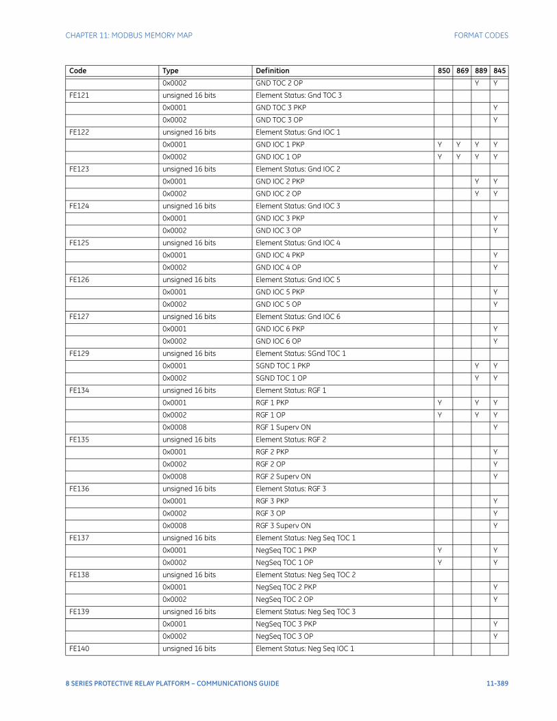
CHAPTER 11: MODBUS MEMORY MAP FORMAT CODES
0x0002 GND TOC 2 OP Y Y
FE121 unsigned 16 bits Element Status: Gnd TOC 3
0x0001 GND TOC 3 PKP Y
0x0002 GND TOC 3 OP Y
FE122 unsigned 16 bits Element Status: Gnd IOC 1
0x0001 GND IOC 1 PKP Y Y Y Y
0x0002 GND IOC 1 OP Y Y Y Y
FE123 unsigned 16 bits Element Status: Gnd IOC 2
0x0001 GND IOC 2 PKP Y Y
0x0002 GND IOC 2 OP Y Y
FE124 unsigned 16 bits Element Status: Gnd IOC 3
0x0001 GND IOC 3 PKP Y
0x0002 GND IOC 3 OP Y
FE125 unsigned 16 bits Element Status: Gnd IOC 4
0x0001 GND IOC 4 PKP Y
0x0002 GND IOC 4 OP Y
FE126 unsigned 16 bits Element Status: Gnd IOC 5
0x0001 GND IOC 5 PKP Y
0x0002 GND IOC 5 OP Y
FE127 unsigned 16 bits Element Status: Gnd IOC 6
0x0001 GND IOC 6 PKP Y
0x0002 GND IOC 6 OP Y
FE129 unsigned 16 bits Element Status: SGnd TOC 1
0x0001 SGND TOC 1 PKP Y Y
0x0002 SGND TOC 1 OP Y Y
FE134 unsigned 16 bits Element Status: RGF 1
0x0001 RGF 1 PKP Y Y Y
0x0002 RGF 1 OP Y Y Y
0x0008 RGF 1 Superv ON Y
FE135 unsigned 16 bits Element Status: RGF 2
0x0001 RGF 2 PKP Y
0x0002 RGF 2 OP Y
0x0008 RGF 2 Superv ON Y
FE136 unsigned 16 bits Element Status: RGF 3
0x0001 RGF 3 PKP Y
0x0002 RGF 3 OP Y
0x0008 RGF 3 Superv ON Y
FE137 unsigned 16 bits Element Status: Neg Seq TOC 1
0x0001 NegSeq TOC 1 PKP Y Y
0x0002 NegSeq TOC 1 OP Y Y
FE138 unsigned 16 bits Element Status: Neg Seq TOC 2
0x0001 NegSeq TOC 2 PKP Y
0x0002 NegSeq TOC 2 OP Y
FE139 unsigned 16 bits Element Status: Neg Seq TOC 3
0x0001 NegSeq TOC 3 PKP Y
0x0002 NegSeq TOC 3 OP Y
FE140 unsigned 16 bits Element Status: Neg Seq IOC 1
Code Type Definition 850 869 889 845
8 SERIES PROTECTIVE RELAY PLATFORM – COMMUNICATIONS GUIDE 11-389
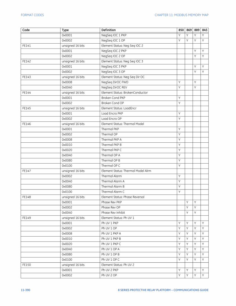
FORMAT CODES CHAPTER 11: MODBUS MEMORY MAP
0x0001 NegSeq IOC 1 PKP Y Y Y Y
0x0002 NegSeq IOC 1 OP Y Y Y Y
FE141 unsigned 16 bits Element Status: Neg Seq IOC 2
0x0001 NegSeq IOC 2 PKP Y Y
0x0002 NegSeq IOC 2 OP Y Y
FE142 unsigned 16 bits Element Status: Neg Seq IOC 3
0x0001 NegSeq IOC 3 PKP Y Y
0x0002 NegSeq IOC 3 OP Y Y
FE143 unsigned 16 bits Element Status: Neg Seq Dir OC
0x0008 NegSeq DirOC FWD Y Y
0x0040 NegSeq DirOC REV Y Y
FE144 unsigned 16 bits Element Status: BrokenConductor
0x0001 Broken Cond PKP Y
0x0002 Broken Cond OP Y
FE145 unsigned 16 bits Element Status: LoadEncr
0x0001 Load Encro PKP Y
0x0002 Load Encro OP Y
FE146 unsigned 16 bits Element Status: Thermal Model
0x0001 Thermal PKP Y
0x0002 Thermal OP Y
0x0008 Thermal PKP A Y
0x0010 Thermal PKP B Y
0x0020 Thermal PKP C Y
0x0040 Thermal OP A Y
0x0080 Thermal OP B Y
0x0100 Thermal OP C Y
FE147 unsigned 16 bits Element Status: Thermal Model Alrm
0x0002 Thermal Alarm Y
0x0040 Thermal Alarm A Y
0x0080 Thermal Alarm B Y
0x0100 Thermal Alarm C Y
FE148 unsigned 16 bits Element Status: Phase Reversal
0x0001 Phase Rev PKP Y Y
0x0002 Phase Rev OP Y Y
0x0040 Phase Rev Inhibit Y Y
FE149 unsigned 16 bits Element Status: Ph UV 1
0x0001 Ph UV 1 PKP Y Y Y Y
0x0002 Ph UV 1 OP Y Y Y Y
0x0008 Ph UV 1 PKP A Y Y Y Y
0x0010 Ph UV 1 PKP B Y Y Y Y
0x0020 Ph UV 1 PKP C Y Y Y Y
0x0040 Ph UV 1 OP A Y Y Y Y
0x0080 Ph UV 1 OP B Y Y Y Y
0x0100 Ph UV 1 OP C Y Y Y Y
FE150 unsigned 16 bits Element Status: Ph UV 2
0x0001 Ph UV 2 PKP Y Y Y Y
0x0002 Ph UV 2 OP Y Y Y Y
Code Type Definition 850 869 889 845
11-390 8 SERIES PROTECTIVE RELAY PLATFORM – COMMUNICATIONS GUIDE
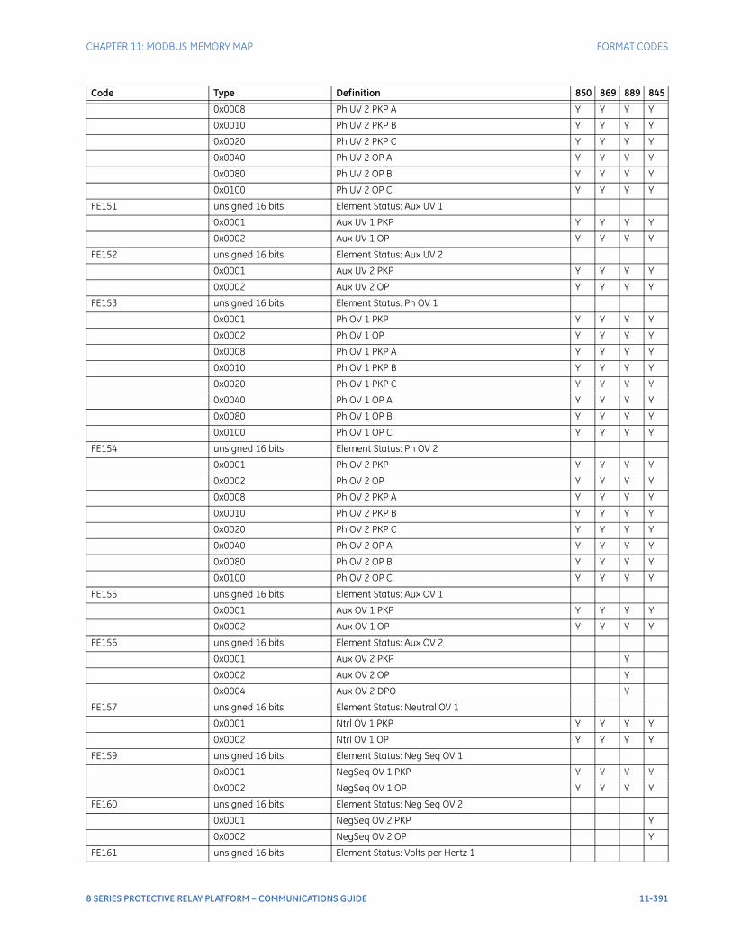
CHAPTER 11: MODBUS MEMORY MAP FORMAT CODES
0x0008 Ph UV 2 PKP A Y Y Y Y
0x0010 Ph UV 2 PKP B Y Y Y Y
0x0020 Ph UV 2 PKP C Y Y Y Y
0x0040 Ph UV 2 OP A Y Y Y Y
0x0080 Ph UV 2 OP B Y Y Y Y
0x0100 Ph UV 2 OP C Y Y Y Y
FE151 unsigned 16 bits Element Status: Aux UV 1
0x0001 Aux UV 1 PKP Y Y Y Y
0x0002 Aux UV 1 OP Y Y Y Y
FE152 unsigned 16 bits Element Status: Aux UV 2
0x0001 Aux UV 2 PKP Y Y Y Y
0x0002 Aux UV 2 OP Y Y Y Y
FE153 unsigned 16 bits Element Status: Ph OV 1
0x0001 Ph OV 1 PKP Y Y Y Y
0x0002 Ph OV 1 OP Y Y Y Y
0x0008 Ph OV 1 PKP A Y Y Y Y
0x0010 Ph OV 1 PKP B Y Y Y Y
0x0020 Ph OV 1 PKP C Y Y Y Y
0x0040 Ph OV 1 OP A Y Y Y Y
0x0080 Ph OV 1 OP B Y Y Y Y
0x0100 Ph OV 1 OP C Y Y Y Y
FE154 unsigned 16 bits Element Status: Ph OV 2
0x0001 Ph OV 2 PKP Y Y Y Y
0x0002 Ph OV 2 OP Y Y Y Y
0x0008 Ph OV 2 PKP A Y Y Y Y
0x0010 Ph OV 2 PKP B Y Y Y Y
0x0020 Ph OV 2 PKP C Y Y Y Y
0x0040 Ph OV 2 OP A Y Y Y Y
0x0080 Ph OV 2 OP B Y Y Y Y
0x0100 Ph OV 2 OP C Y Y Y Y
FE155 unsigned 16 bits Element Status: Aux OV 1
0x0001 Aux OV 1 PKP Y Y Y Y
0x0002 Aux OV 1 OP Y Y Y Y
FE156 unsigned 16 bits Element Status: Aux OV 2
0x0001 Aux OV 2 PKP Y
0x0002 Aux OV 2 OP Y
0x0004 Aux OV 2 DPO Y
FE157 unsigned 16 bits Element Status: Neutral OV 1
0x0001 Ntrl OV 1 PKP Y Y Y Y
0x0002 Ntrl OV 1 OP Y Y Y Y
FE159 unsigned 16 bits Element Status: Neg Seq OV 1
0x0001 NegSeq OV 1 PKP Y Y Y Y
0x0002 NegSeq OV 1 OP Y Y Y Y
FE160 unsigned 16 bits Element Status: Neg Seq OV 2
0x0001 NegSeq OV 2 PKP Y
0x0002 NegSeq OV 2 OP Y
FE161 unsigned 16 bits Element Status: Volts per Hertz 1
Code Type Definition 850 869 889 845
8 SERIES PROTECTIVE RELAY PLATFORM – COMMUNICATIONS GUIDE 11-391
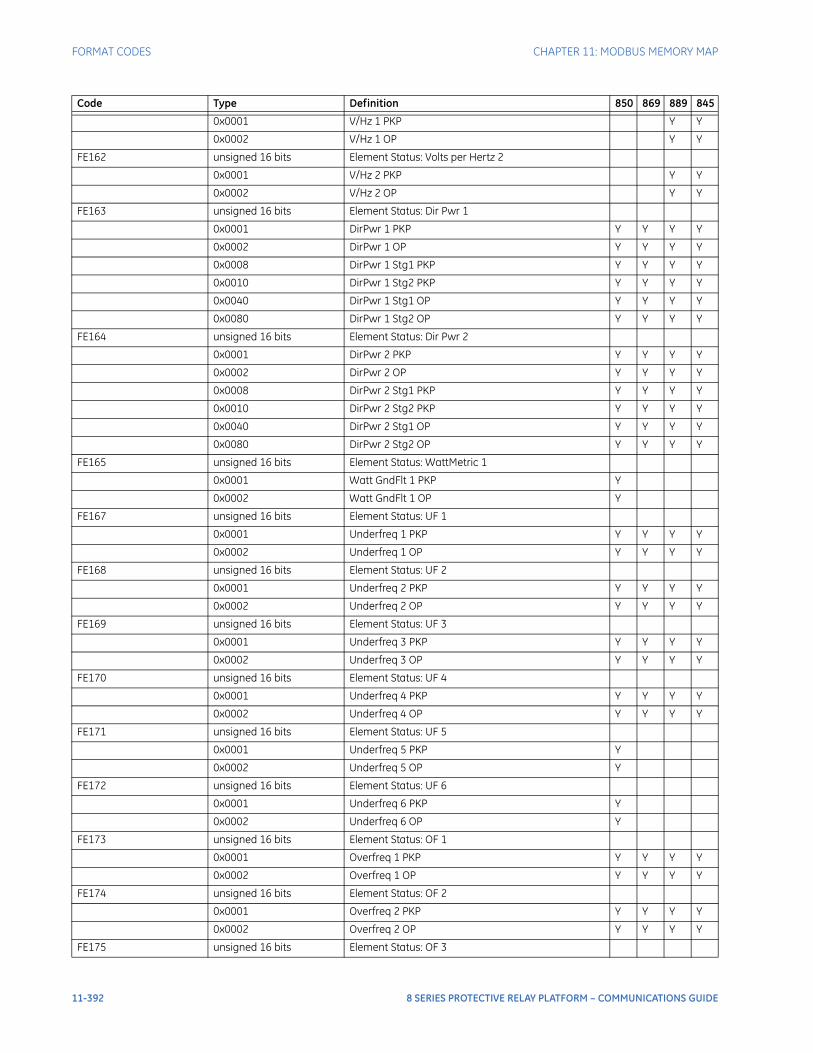
FORMAT CODES CHAPTER 11: MODBUS MEMORY MAP
0x0001 V/Hz 1 PKP Y Y
0x0002 V/Hz 1 OP Y Y
FE162 unsigned 16 bits Element Status: Volts per Hertz 2
0x0001 V/Hz 2 PKP Y Y
0x0002 V/Hz 2 OP Y Y
FE163 unsigned 16 bits Element Status: Dir Pwr 1
0x0001 DirPwr 1 PKP Y Y Y Y
0x0002 DirPwr 1 OP Y Y Y Y
0x0008 DirPwr 1 Stg1 PKP Y Y Y Y
0x0010 DirPwr 1 Stg2 PKP Y Y Y Y
0x0040 DirPwr 1 Stg1 OP Y Y Y Y
0x0080 DirPwr 1 Stg2 OP Y Y Y Y
FE164 unsigned 16 bits Element Status: Dir Pwr 2
0x0001 DirPwr 2 PKP Y Y Y Y
0x0002 DirPwr 2 OP Y Y Y Y
0x0008 DirPwr 2 Stg1 PKP Y Y Y Y
0x0010 DirPwr 2 Stg2 PKP Y Y Y Y
0x0040 DirPwr 2 Stg1 OP Y Y Y Y
0x0080 DirPwr 2 Stg2 OP Y Y Y Y
FE165 unsigned 16 bits Element Status: WattMetric 1
0x0001 Watt GndFlt 1 PKP Y
0x0002 Watt GndFlt 1 OP Y
FE167 unsigned 16 bits Element Status: UF 1
0x0001 Underfreq 1 PKP Y Y Y Y
0x0002 Underfreq 1 OP Y Y Y Y
FE168 unsigned 16 bits Element Status: UF 2
0x0001 Underfreq 2 PKP Y Y Y Y
0x0002 Underfreq 2 OP Y Y Y Y
FE169 unsigned 16 bits Element Status: UF 3
0x0001 Underfreq 3 PKP Y Y Y Y
0x0002 Underfreq 3 OP Y Y Y Y
FE170 unsigned 16 bits Element Status: UF 4
0x0001 Underfreq 4 PKP Y Y Y Y
0x0002 Underfreq 4 OP Y Y Y Y
FE171 unsigned 16 bits Element Status: UF 5
0x0001 Underfreq 5 PKP Y
0x0002 Underfreq 5 OP Y
FE172 unsigned 16 bits Element Status: UF 6
0x0001 Underfreq 6 PKP Y
0x0002 Underfreq 6 OP Y
FE173 unsigned 16 bits Element Status: OF 1
0x0001 Overfreq 1 PKP Y Y Y Y
0x0002 Overfreq 1 OP Y Y Y Y
FE174 unsigned 16 bits Element Status: OF 2
0x0001 Overfreq 2 PKP Y Y Y Y
0x0002 Overfreq 2 OP Y Y Y Y
FE175 unsigned 16 bits Element Status: OF 3
Code Type Definition 850 869 889 845
11-392 8 SERIES PROTECTIVE RELAY PLATFORM – COMMUNICATIONS GUIDE
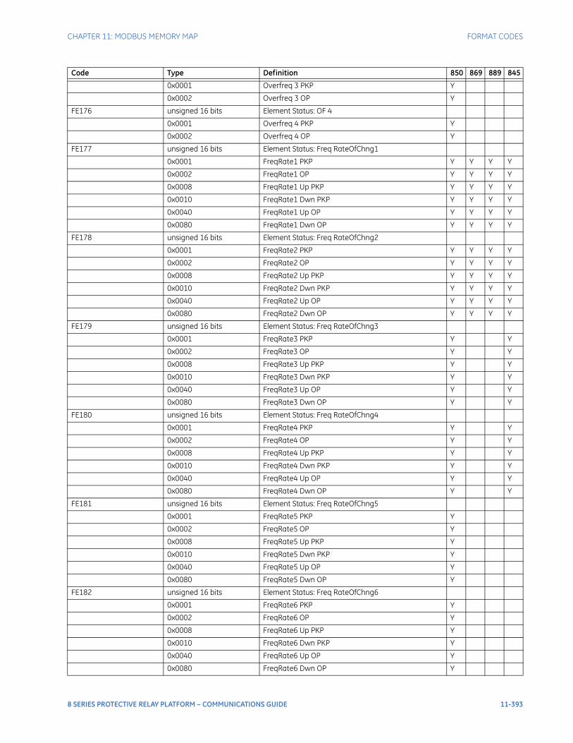
CHAPTER 11: MODBUS MEMORY MAP FORMAT CODES
0x0001 Overfreq 3 PKP Y
0x0002 Overfreq 3 OP Y
FE176 unsigned 16 bits Element Status: OF 4
0x0001 Overfreq 4 PKP Y
0x0002 Overfreq 4 OP Y
FE177 unsigned 16 bits Element Status: Freq RateOfChng1
0x0001 FreqRate1 PKP Y Y Y Y
0x0002 FreqRate1 OP Y Y Y Y
0x0008 FreqRate1 Up PKP Y Y Y Y
0x0010 FreqRate1 Dwn PKP Y Y Y Y
0x0040 FreqRate1 Up OP Y Y Y Y
0x0080 FreqRate1 Dwn OP Y Y Y Y
FE178 unsigned 16 bits Element Status: Freq RateOfChng2
0x0001 FreqRate2 PKP Y Y Y Y
0x0002 FreqRate2 OP Y Y Y Y
0x0008 FreqRate2 Up PKP Y Y Y Y
0x0010 FreqRate2 Dwn PKP Y Y Y Y
0x0040 FreqRate2 Up OP Y Y Y Y
0x0080 FreqRate2 Dwn OP Y Y Y Y
FE179 unsigned 16 bits Element Status: Freq RateOfChng3
0x0001 FreqRate3 PKP Y Y
0x0002 FreqRate3 OP Y Y
0x0008 FreqRate3 Up PKP Y Y
0x0010 FreqRate3 Dwn PKP Y Y
0x0040 FreqRate3 Up OP Y Y
0x0080 FreqRate3 Dwn OP Y Y
FE180 unsigned 16 bits Element Status: Freq RateOfChng4
0x0001 FreqRate4 PKP Y Y
0x0002 FreqRate4 OP Y Y
0x0008 FreqRate4 Up PKP Y Y
0x0010 FreqRate4 Dwn PKP Y Y
0x0040 FreqRate4 Up OP Y Y
0x0080 FreqRate4 Dwn OP Y Y
FE181 unsigned 16 bits Element Status: Freq RateOfChng5
0x0001 FreqRate5 PKP Y
0x0002 FreqRate5 OP Y
0x0008 FreqRate5 Up PKP Y
0x0010 FreqRate5 Dwn PKP Y
0x0040 FreqRate5 Up OP Y
0x0080 FreqRate5 Dwn OP Y
FE182 unsigned 16 bits Element Status: Freq RateOfChng6
0x0001 FreqRate6 PKP Y
0x0002 FreqRate6 OP Y
0x0008 FreqRate6 Up PKP Y
0x0010 FreqRate6 Dwn PKP Y
0x0040 FreqRate6 Up OP Y
0x0080 FreqRate6 Dwn OP Y
Code Type Definition 850 869 889 845
8 SERIES PROTECTIVE RELAY PLATFORM – COMMUNICATIONS GUIDE 11-393
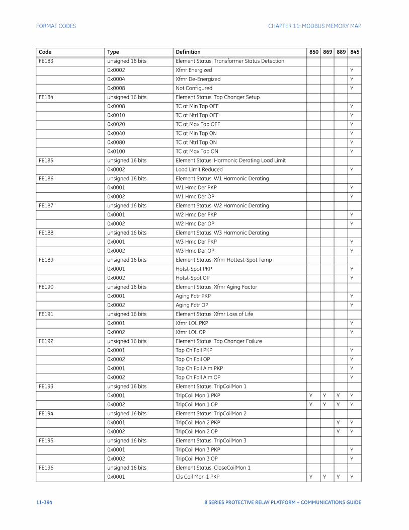
FORMAT CODES CHAPTER 11: MODBUS MEMORY MAP
FE183 unsigned 16 bits Element Status: Transformer Status Detection
0x0002 Xfmr Energized Y
0x0004 Xfmr De-Energized Y
0x0008 Not Configured Y
FE184 unsigned 16 bits Element Status: Tap Changer Setup
0x0008 TC at Min Tap OFF Y
0x0010 TC at Ntrl Tap OFF Y
0x0020 TC at Max Tap OFF Y
0x0040 TC at Min Tap ON Y
0x0080 TC at Ntrl Tap ON Y
0x0100 TC at Max Tap ON Y
FE185 unsigned 16 bits Element Status: Harmonic Derating Load Limit
0x0002 Load Limit Reduced Y
FE186 unsigned 16 bits Element Status: W1 Harmonic Derating
0x0001 W1 Hmc Der PKP Y
0x0002 W1 Hmc Der OP Y
FE187 unsigned 16 bits Element Status: W2 Harmonic Derating
0x0001 W2 Hmc Der PKP Y
0x0002 W2 Hmc Der OP Y
FE188 unsigned 16 bits Element Status: W3 Harmonic Derating
0x0001 W3 Hmc Der PKP Y
0x0002 W3 Hmc Der OP Y
FE189 unsigned 16 bits Element Status: Xfmr Hottest-Spot Temp
0x0001 Hotst-Spot PKP Y
0x0002 Hotst-Spot OP Y
FE190 unsigned 16 bits Element Status: Xfmr Aging Factor
0x0001 Aging Fctr PKP Y
0x0002 Aging Fctr OP Y
FE191 unsigned 16 bits Element Status: Xfmr Loss of Life
0x0001 Xfmr LOL PKP Y
0x0002 Xfmr LOL OP Y
FE192 unsigned 16 bits Element Status: Tap Changer Failure
0x0001 Tap Ch Fail PKP Y
0x0002 Tap Ch Fail OP Y
0x0001 Tap Ch Fail Alm PKP Y
0x0002 Tap Ch Fail Alm OP Y
FE193 unsigned 16 bits Element Status: TripCoilMon 1
0x0001 TripCoil Mon 1 PKP Y Y Y Y
0x0002 TripCoil Mon 1 OP Y Y Y Y
FE194 unsigned 16 bits Element Status: TripCoilMon 2
0x0001 TripCoil Mon 2 PKP Y Y
0x0002 TripCoil Mon 2 OP Y Y
FE195 unsigned 16 bits Element Status: TripCoilMon 3
0x0001 TripCoil Mon 3 PKP Y
0x0002 TripCoil Mon 3 OP Y
FE196 unsigned 16 bits Element Status: CloseCoilMon 1
0x0001 Cls Coil Mon 1 PKP Y Y Y Y
Code Type Definition 850 869 889 845
11-394 8 SERIES PROTECTIVE RELAY PLATFORM – COMMUNICATIONS GUIDE

CHAPTER 11: MODBUS MEMORY MAP FORMAT CODES
0x0002 Cls Coil Mon 1 OP Y Y Y Y
FE197 unsigned 16 bits Element Status: CloseCoilMon 2
0x0001 Cls Coil Mon 2 PKP Y Y
0x0002 Cls Coil Mon 2 OP Y Y
FE198 unsigned 16 bits Element Status: CloseCoilMon 3
0x0001 Cls Coil Mon 3 PKP Y
0x0002 Cls Coil Mon 3 OP Y
FE199 unsigned 16 bits Element Status: Breaker 1 Arcing Current
0x0002 BKR1 Arc OP Y Y Y Y
FE200 unsigned 16 bits Element Status: Breaker 2 Arcing Current
0x0002 BKR2 Arc OP Y Y
FE201 unsigned 16 bits Element Status: Breaker 3 Arcing Current
0x0002 BKR3 Arc OP Y
FE202 unsigned 16 bits Element Status: Breaker1 Health
0x0001 BKR1 Charge Fail Y Y Y Y
0x0002 BKR1 Hlth PKP Y Y Y Y
0x0008 BKR1 Hlth Trip PKP Y Y Y Y
0x0010 BKR1 Hlth Cls PKP Y Y Y Y
0x0020 BKR1 Hlth Chg PKP Y Y Y Y
0x0040 BKR1 Hlth OP Fail Y Y Y Y
FE203 unsigned 16 bits Element Status: Breaker2 Health
0x0001 BKR2 Charge Fail Y
0x0002 BKR2 Hlth PKP Y
0x0008 BKR2 Hlth Trip PKP Y
0x0010 BKR2 Hlth Cls PKP Y
0x0020 BKR2 Hlth Chg PKP Y
0x0040 BKR2 Hlth OP Fail Y
FE204 unsigned 16 bits Element Status: Breaker3 Health
0x0001 BKR3 Charge Fail Y
0x0002 BKR3 Hlth PKP Y
0x0008 BKR3 Hlth Trip PKP Y
0x0010 BKR3 Hlth Cls PKP Y
0x0020 BKR3 Hlth Chg PKP Y
0x0040 BKR3 Hlth OP Fail Y
FE205 unsigned 16 bits Element Status: Breaker1 Arc Health
0x0001 BKR1 Arc Fail Y Y Y Y
0x0008 BKR1 Arc PKP A Y Y Y Y
0x0010 BKR1 Arc PKP B Y Y Y Y
0x0020 BKR1 Arc PKP C Y Y Y Y
0x0040 BKR1 Engy PKP A Y Y Y Y
0x0080 BKR1 Engy PKP B Y Y Y Y
0x0100 BKR1 Engy PKP C Y Y Y Y
FE206 unsigned 16 bits Element Status: Breaker2 Arc Health
0x0001 BKR2 Arc Fail Y Y
0x0008 BKR2 Arc PKP A Y Y
0x0010 BKR2 Arc PKP B Y Y
0x0020 BKR2 Arc PKP C Y Y
Code Type Definition 850 869 889 845
8 SERIES PROTECTIVE RELAY PLATFORM – COMMUNICATIONS GUIDE 11-395
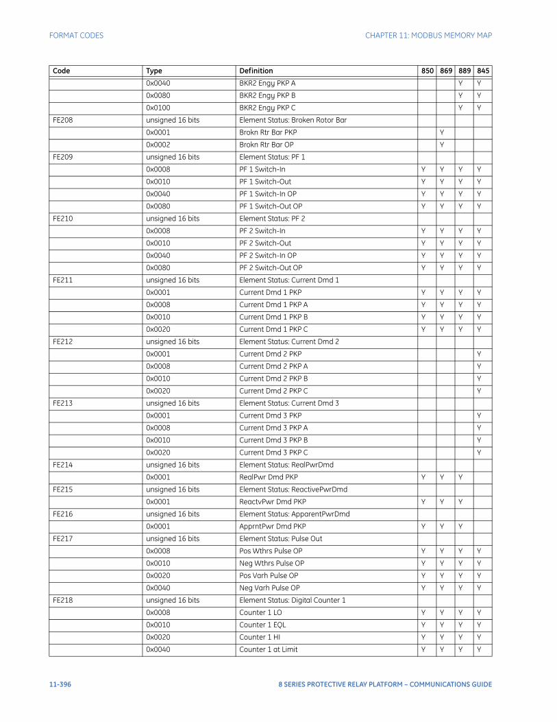
FORMAT CODES CHAPTER 11: MODBUS MEMORY MAP
0x0040 BKR2 Engy PKP A Y Y
0x0080 BKR2 Engy PKP B Y Y
0x0100 BKR2 Engy PKP C Y Y
FE208 unsigned 16 bits Element Status: Broken Rotor Bar
0x0001 Brokn Rtr Bar PKP Y
0x0002 Brokn Rtr Bar OP Y
FE209 unsigned 16 bits Element Status: PF 1
0x0008 PF 1 Switch-In Y Y Y Y
0x0010 PF 1 Switch-Out Y Y Y Y
0x0040 PF 1 Switch-In OP Y Y Y Y
0x0080 PF 1 Switch-Out OP Y Y Y Y
FE210 unsigned 16 bits Element Status: PF 2
0x0008 PF 2 Switch-In Y Y Y Y
0x0010 PF 2 Switch-Out Y Y Y Y
0x0040 PF 2 Switch-In OP Y Y Y Y
0x0080 PF 2 Switch-Out OP Y Y Y Y
FE211 unsigned 16 bits Element Status: Current Dmd 1
0x0001 Current Dmd 1 PKP Y Y Y Y
0x0008 Current Dmd 1 PKP A Y Y Y Y
0x0010 Current Dmd 1 PKP B Y Y Y Y
0x0020 Current Dmd 1 PKP C Y Y Y Y
FE212 unsigned 16 bits Element Status: Current Dmd 2
0x0001 Current Dmd 2 PKP Y
0x0008 Current Dmd 2 PKP A Y
0x0010 Current Dmd 2 PKP B Y
0x0020 Current Dmd 2 PKP C Y
FE213 unsigned 16 bits Element Status: Current Dmd 3
0x0001 Current Dmd 3 PKP Y
0x0008 Current Dmd 3 PKP A Y
0x0010 Current Dmd 3 PKP B Y
0x0020 Current Dmd 3 PKP C Y
FE214 unsigned 16 bits Element Status: RealPwrDmd
0x0001 RealPwr Dmd PKP Y Y Y
FE215 unsigned 16 bits Element Status: ReactivePwrDmd
0x0001 ReactvPwr Dmd PKP Y Y Y
FE216 unsigned 16 bits Element Status: ApparentPwrDmd
0x0001 ApprntPwr Dmd PKP Y Y Y
FE217 unsigned 16 bits Element Status: Pulse Out
0x0008 Pos Wthrs Pulse OP Y Y Y Y
0x0010 Neg Wthrs Pulse OP Y Y Y Y
0x0020 Pos Varh Pulse OP Y Y Y Y
0x0040 Neg Varh Pulse OP Y Y Y Y
FE218 unsigned 16 bits Element Status: Digital Counter 1
0x0008 Counter 1 LO Y Y Y Y
0x0010 Counter 1 EQL Y Y Y Y
0x0020 Counter 1 HI Y Y Y Y
0x0040 Counter 1 at Limit Y Y Y Y
Code Type Definition 850 869 889 845
11-396 8 SERIES PROTECTIVE RELAY PLATFORM – COMMUNICATIONS GUIDE
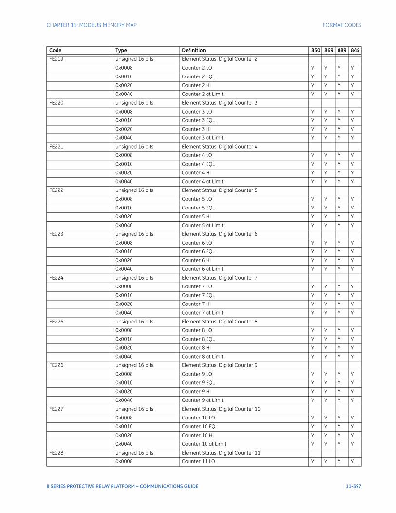
CHAPTER 11: MODBUS MEMORY MAP FORMAT CODES
FE219 unsigned 16 bits Element Status: Digital Counter 2
0x0008 Counter 2 LO Y Y Y Y
0x0010 Counter 2 EQL Y Y Y Y
0x0020 Counter 2 HI Y Y Y Y
0x0040 Counter 2 at Limit Y Y Y Y
FE220 unsigned 16 bits Element Status: Digital Counter 3
0x0008 Counter 3 LO Y Y Y Y
0x0010 Counter 3 EQL Y Y Y Y
0x0020 Counter 3 HI Y Y Y Y
0x0040 Counter 3 at Limit Y Y Y Y
FE221 unsigned 16 bits Element Status: Digital Counter 4
0x0008 Counter 4 LO Y Y Y Y
0x0010 Counter 4 EQL Y Y Y Y
0x0020 Counter 4 HI Y Y Y Y
0x0040 Counter 4 at Limit Y Y Y Y
FE222 unsigned 16 bits Element Status: Digital Counter 5
0x0008 Counter 5 LO Y Y Y Y
0x0010 Counter 5 EQL Y Y Y Y
0x0020 Counter 5 HI Y Y Y Y
0x0040 Counter 5 at Limit Y Y Y Y
FE223 unsigned 16 bits Element Status: Digital Counter 6
0x0008 Counter 6 LO Y Y Y Y
0x0010 Counter 6 EQL Y Y Y Y
0x0020 Counter 6 HI Y Y Y Y
0x0040 Counter 6 at Limit Y Y Y Y
FE224 unsigned 16 bits Element Status: Digital Counter 7
0x0008 Counter 7 LO Y Y Y Y
0x0010 Counter 7 EQL Y Y Y Y
0x0020 Counter 7 HI Y Y Y Y
0x0040 Counter 7 at Limit Y Y Y Y
FE225 unsigned 16 bits Element Status: Digital Counter 8
0x0008 Counter 8 LO Y Y Y Y
0x0010 Counter 8 EQL Y Y Y Y
0x0020 Counter 8 HI Y Y Y Y
0x0040 Counter 8 at Limit Y Y Y Y
FE226 unsigned 16 bits Element Status: Digital Counter 9
0x0008 Counter 9 LO Y Y Y Y
0x0010 Counter 9 EQL Y Y Y Y
0x0020 Counter 9 HI Y Y Y Y
0x0040 Counter 9 at Limit Y Y Y Y
FE227 unsigned 16 bits Element Status: Digital Counter 10
0x0008 Counter 10 LO Y Y Y Y
0x0010 Counter 10 EQL Y Y Y Y
0x0020 Counter 10 HI Y Y Y Y
0x0040 Counter 10 at Limit Y Y Y Y
FE228 unsigned 16 bits Element Status: Digital Counter 11
0x0008 Counter 11 LO Y Y Y Y
Code Type Definition 850 869 889 845
8 SERIES PROTECTIVE RELAY PLATFORM – COMMUNICATIONS GUIDE 11-397

FORMAT CODES CHAPTER 11: MODBUS MEMORY MAP
0x0010 Counter 11 EQL Y Y Y Y
0x0020 Counter 11 HI Y Y Y Y
0x0040 Counter 11 at Limit Y Y Y Y
FE229 unsigned 16 bits Element Status: Digital Counter 12
0x0008 Counter 12 LO Y Y Y Y
0x0010 Counter 12 EQL Y Y Y Y
0x0020 Counter 12 HI Y Y Y Y
0x0040 Counter 12 at Limit Y Y Y Y
FE230 unsigned 16 bits Element Status: Digital Counter 13
0x0008 Counter 13 LO Y Y Y Y
0x0010 Counter 13 EQL Y Y Y Y
0x0020 Counter 13 HI Y Y Y Y
0x0040 Counter 13 at Limit Y Y Y Y
FE231 unsigned 16 bits Element Status: Digital Counter 14
0x0008 Counter 14 LO Y Y Y Y
0x0010 Counter 14 EQL Y Y Y Y
0x0020 Counter 14 HI Y Y Y Y
0x0040 Counter 14 at Limit Y Y Y Y
FE232 unsigned 16 bits Element Status: Digital Counter 15
0x0008 Counter 15 LO Y Y Y Y
0x0010 Counter 15 EQL Y Y Y Y
0x0020 Counter 15 HI Y Y Y Y
0x0040 Counter 15 at Limit Y Y Y Y
FE233 unsigned 16 bits Element Status: Digital Counter 16
0x0008 Counter 16 LO Y Y Y Y
0x0010 Counter 16 EQL Y Y Y Y
0x0020 Counter 16 HI Y Y Y Y
0x0040 Counter 16 at Limit Y Y Y Y
FE234 unsigned 16 bits Element Status: Harmonic Detection 1
0x0001 Harm Det 1 PKP Y Y Y Y
0x0002 Harm Det 1 OP Y Y Y Y
FE235 unsigned 16 bits Element Status: Harmonic Detection 2
0x0001 Harm Det 2 PKP Y Y Y Y
0x0002 Harm Det 2 OP Y Y Y Y
FE236 unsigned 16 bits Element Status: Harmonic Detection 3
0x0001 Harm Det 3 PKP Y Y Y Y
0x0002 Harm Det 3 OP Y Y Y Y
FE237 unsigned 16 bits Element Status: Harmonic Detection 4
0x0001 Harm Det 4 PKP Y Y Y Y
0x0002 Harm Det 4 OP Y Y Y Y
FE238 unsigned 16 bits Element Status: Harmonic Detection 5
0x0001 Harm Det 5 PKP Y Y Y Y
0x0002 Harm Det 5 OP Y Y Y Y
FE239 unsigned 16 bits Element Status: Harmonic Detection 6
0x0001 Harm Det 6 PKP Y Y Y Y
0x0002 Harm Det 6 OP Y Y Y Y
FE240 unsigned 16 bits Element Status: Start Inhibit
Code Type Definition 850 869 889 845
11-398 8 SERIES PROTECTIVE RELAY PLATFORM – COMMUNICATIONS GUIDE
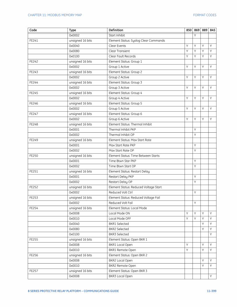
CHAPTER 11: MODBUS MEMORY MAP FORMAT CODES
0x0002 Start Inhibit Y
FE241 unsigned 16 bits Element Status: Syslog Clear Commands
0x0040 Clear Events Y Y Y Y
0x0080 Clear Transient Y Y Y Y
0x0100 Clear Fault Records Y Y Y Y
FE242 unsigned 16 bits Element Status: Group 1
0x0002 Group 1 Active Y Y Y Y
FE243 unsigned 16 bits Element Status: Group 2
0x0002 Group 2 Active Y Y Y Y
FE244 unsigned 16 bits Element Status: Group 3
0x0002 Group 3 Active Y Y Y Y
FE245 unsigned 16 bits Element Status: Group 4
0x0002 Group 4 Active Y Y Y Y
FE246 unsigned 16 bits Element Status: Group 5
0x0002 Group 5 Active Y Y Y Y
FE247 unsigned 16 bits Element Status: Group 6
0x0002 Group 6 Active Y Y Y Y
FE248 unsigned 16 bits Element Status: Thermal Inhibit
0x0001 Thermal Inhibit PKP Y
0x0002 Thermal Inhibit OP Y
FE249 unsigned 16 bits Element Status: Max Start Rate
0x0001 Max Start Rate PKP Y
0x0002 Max Start Rate OP Y
FE250 unsigned 16 bits Element Status: Time Between Starts
0x0001 Time Btwn Star PKP Y
0x0002 Time Btwn Start OP Y
FE251 unsigned 16 bits Element Status: Restart Delay
0x0001 Restart Delay PKP Y
0x0002 Restart Delay OP Y
FE252 unsigned 16 bits Element Status: Reduced Voltage Start
0x0002 Reduced Volt Ctrl Y
FE253 unsigned 16 bits Element Status: Reduced Voltage Fail
0x0002 Reduced Volt Fail Y
FE254 unsigned 16 bits Element Status: Local Mode
0x0008 Local Mode ON Y Y Y Y
0x0010 Local Mode OFF Y Y Y Y
0x0040 BKR1 Selected Y Y
0x0080 BKR2 Selected Y Y
0x0100 BKR3 Selected Y
FE255 unsigned 16 bits Element Status: Open BKR 1
0x0008 BKR1 Local Open Y Y Y
0x0010 BKR1 Remote Open Y Y Y
FE256 unsigned 16 bits Element Status: Open BKR 2
0x0008 BKR2 Local Open Y Y
0x0010 BKR2 Remote Open Y Y
FE257 unsigned 16 bits Element Status: Open BKR 3
0x0008 BKR3 Local Open Y
Code Type Definition 850 869 889 845
8 SERIES PROTECTIVE RELAY PLATFORM – COMMUNICATIONS GUIDE 11-399
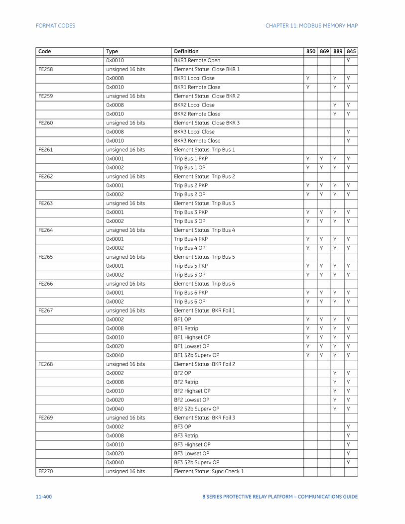
FORMAT CODES CHAPTER 11: MODBUS MEMORY MAP
0x0010 BKR3 Remote Open Y
FE258 unsigned 16 bits Element Status: Close BKR 1
0x0008 BKR1 Local Close Y Y Y
0x0010 BKR1 Remote Close Y Y Y
FE259 unsigned 16 bits Element Status: Close BKR 2
0x0008 BKR2 Local Close Y Y
0x0010 BKR2 Remote Close Y Y
FE260 unsigned 16 bits Element Status: Close BKR 3
0x0008 BKR3 Local Close Y
0x0010 BKR3 Remote Close Y
FE261 unsigned 16 bits Element Status: Trip Bus 1
0x0001 Trip Bus 1 PKP Y Y Y Y
0x0002 Trip Bus 1 OP Y Y Y Y
FE262 unsigned 16 bits Element Status: Trip Bus 2
0x0001 Trip Bus 2 PKP Y Y Y Y
0x0002 Trip Bus 2 OP Y Y Y Y
FE263 unsigned 16 bits Element Status: Trip Bus 3
0x0001 Trip Bus 3 PKP Y Y Y Y
0x0002 Trip Bus 3 OP Y Y Y Y
FE264 unsigned 16 bits Element Status: Trip Bus 4
0x0001 Trip Bus 4 PKP Y Y Y Y
0x0002 Trip Bus 4 OP Y Y Y Y
FE265 unsigned 16 bits Element Status: Trip Bus 5
0x0001 Trip Bus 5 PKP Y Y Y Y
0x0002 Trip Bus 5 OP Y Y Y Y
FE266 unsigned 16 bits Element Status: Trip Bus 6
0x0001 Trip Bus 6 PKP Y Y Y Y
0x0002 Trip Bus 6 OP Y Y Y Y
FE267 unsigned 16 bits Element Status: BKR Fail 1
0x0002 BF1 OP Y Y Y Y
0x0008 BF1 Retrip Y Y Y Y
0x0010 BF1 Highset OP Y Y Y Y
0x0020 BF1 Lowset OP Y Y Y Y
0x0040 BF1 52b Superv OP Y Y Y Y
FE268 unsigned 16 bits Element Status: BKR Fail 2
0x0002 BF2 OP Y Y
0x0008 BF2 Retrip Y Y
0x0010 BF2 Highset OP Y Y
0x0020 BF2 Lowset OP Y Y
0x0040 BF2 52b Superv OP Y Y
FE269 unsigned 16 bits Element Status: BKR Fail 3
0x0002 BF3 OP Y
0x0008 BF3 Retrip Y
0x0010 BF3 Highset OP Y
0x0020 BF3 Lowset OP Y
0x0040 BF3 52b Superv OP Y
FE270 unsigned 16 bits Element Status: Sync Check 1
Code Type Definition 850 869 889 845
11-400 8 SERIES PROTECTIVE RELAY PLATFORM – COMMUNICATIONS GUIDE
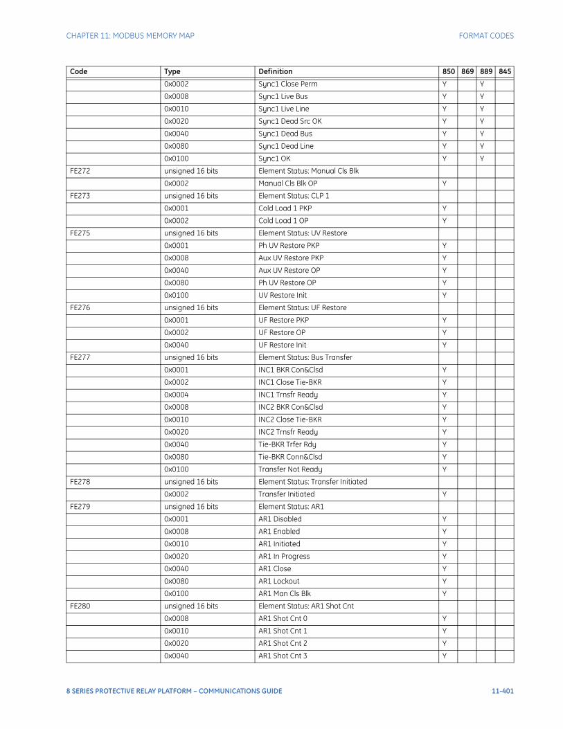
CHAPTER 11: MODBUS MEMORY MAP FORMAT CODES
0x0002 Sync1 Close Perm Y Y
0x0008 Sync1 Live Bus Y Y
0x0010 Sync1 Live Line Y Y
0x0020 Sync1 Dead Src OK Y Y
0x0040 Sync1 Dead Bus Y Y
0x0080 Sync1 Dead Line Y Y
0x0100 Sync1 OK Y Y
FE272 unsigned 16 bits Element Status: Manual Cls Blk
0x0002 Manual Cls Blk OP Y
FE273 unsigned 16 bits Element Status: CLP 1
0x0001 Cold Load 1 PKP Y
0x0002 Cold Load 1 OP Y
FE275 unsigned 16 bits Element Status: UV Restore
0x0001 Ph UV Restore PKP Y
0x0008 Aux UV Restore PKP Y
0x0040 Aux UV Restore OP Y
0x0080 Ph UV Restore OP Y
0x0100 UV Restore Init Y
FE276 unsigned 16 bits Element Status: UF Restore
0x0001 UF Restore PKP Y
0x0002 UF Restore OP Y
0x0040 UF Restore Init Y
FE277 unsigned 16 bits Element Status: Bus Transfer
0x0001 INC1 BKR Con&Clsd Y
0x0002 INC1 Close Tie-BKR Y
0x0004 INC1 Trnsfr Ready Y
0x0008 INC2 BKR Con&Clsd Y
0x0010 INC2 Close Tie-BKR Y
0x0020 INC2 Trnsfr Ready Y
0x0040 Tie-BKR Trfer Rdy Y
0x0080 Tie-BKR Conn&Clsd Y
0x0100 Transfer Not Ready Y
FE278 unsigned 16 bits Element Status: Transfer Initiated
0x0002 Transfer Initiated Y
FE279 unsigned 16 bits Element Status: AR1
0x0001 AR1 Disabled Y
0x0008 AR1 Enabled Y
0x0010 AR1 Initiated Y
0x0020 AR1 In Progress Y
0x0040 AR1 Close Y
0x0080 AR1 Lockout Y
0x0100 AR1 Man Cls Blk Y
FE280 unsigned 16 bits Element Status: AR1 Shot Cnt
0x0008 AR1 Shot Cnt 0 Y
0x0010 AR1 Shot Cnt 1 Y
0x0020 AR1 Shot Cnt 2 Y
0x0040 AR1 Shot Cnt 3 Y
Code Type Definition 850 869 889 845
8 SERIES PROTECTIVE RELAY PLATFORM – COMMUNICATIONS GUIDE 11-401
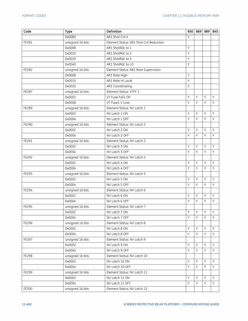
FORMAT CODES CHAPTER 11: MODBUS MEMORY MAP
0x0080 AR1 Shot Cnt 4 Y
FE281 unsigned 16 bits Element Status: AR1 Shot Cnt Reduction
0x0008 AR1 ShotRdc to 1 Y
0x0010 AR1 ShotRdc to 2 Y
0x0020 AR1 ShotRdc to 3 Y
0x0040 AR1 ShotRdc to LO Y
FE282 unsigned 16 bits Element Status: AR1 Rate Supervision
0x0008 AR1 Rate High Y
0x0010 AR1 Rate HI Lockt Y
0x0020 AR1 Coordinating Y
FE287 unsigned 16 bits Element Status: VTFF 1
0x0002 VT Fuse Fail1 OP Y Y Y Y
0x0008 VT Fuse1 V Loss Y Y Y Y
FE289 unsigned 16 bits Element Status: NV Latch 1
0x0002 NV Latch 1 ON Y Y Y Y
0x0004 NV Latch 1 OFF Y Y Y Y
FE290 unsigned 16 bits Element Status: NV Latch 2
0x0002 NV Latch 2 ON Y Y Y Y
0x0004 NV Latch 2 OFF Y Y Y Y
FE291 unsigned 16 bits Element Status: NV Latch 3
0x0002 NV Latch 3 ON Y Y Y Y
0x0004 NV Latch 3 OFF Y Y Y Y
FE292 unsigned 16 bits Element Status: NV Latch 4
0x0002 NV Latch 4 ON Y Y Y Y
0x0004 NV Latch 4 OFF Y Y Y Y
FE293 unsigned 16 bits Element Status: NV Latch 5
0x0002 NV Latch 5 ON Y Y Y Y
0x0004 NV Latch 5 OFF Y Y Y Y
FE294 unsigned 16 bits Element Status: NV Latch 6
0x0002 NV Latch 6 ON Y Y Y Y
0x0004 NV Latch 6 OFF Y Y Y Y
FE295 unsigned 16 bits Element Status: NV Latch 7
0x0002 NV Latch 7 ON Y Y Y Y
0x0004 NV Latch 7 OFF Y Y Y Y
FE296 unsigned 16 bits Element Status: NV Latch 8
0x0002 NV Latch 8 ON Y Y Y Y
0x0004 NV Latch 8 OFF Y Y Y Y
FE297 unsigned 16 bits Element Status: NV Latch 9
0x0002 NV Latch 9 ON Y Y Y Y
0x0004 NV Latch 9 OFF Y Y Y Y
FE298 unsigned 16 bits Element Status: NV Latch 10
0x0002 NV Latch 10 ON Y Y Y Y
0x0004 NV Latch 10 OFF Y Y Y Y
FE299 unsigned 16 bits Element Status: NV Latch 11
0x0002 NV Latch 11 ON Y Y Y Y
0x0004 NV Latch 11 OFF Y Y Y Y
FE300 unsigned 16 bits Element Status: NV Latch 12
Code Type Definition 850 869 889 845
11-402 8 SERIES PROTECTIVE RELAY PLATFORM – COMMUNICATIONS GUIDE
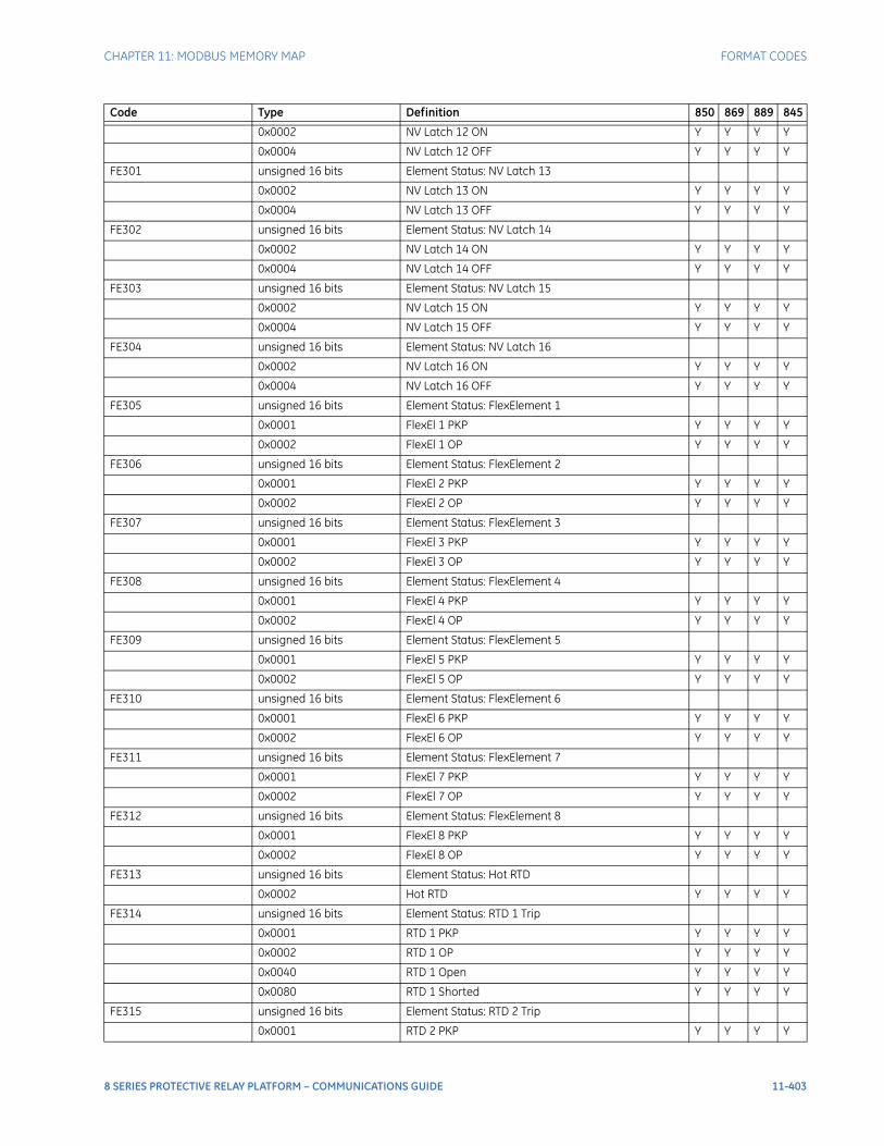
CHAPTER 11: MODBUS MEMORY MAP FORMAT CODES
0x0002 NV Latch 12 ON Y Y Y Y
0x0004 NV Latch 12 OFF Y Y Y Y
FE301 unsigned 16 bits Element Status: NV Latch 13
0x0002 NV Latch 13 ON Y Y Y Y
0x0004 NV Latch 13 OFF Y Y Y Y
FE302 unsigned 16 bits Element Status: NV Latch 14
0x0002 NV Latch 14 ON Y Y Y Y
0x0004 NV Latch 14 OFF Y Y Y Y
FE303 unsigned 16 bits Element Status: NV Latch 15
0x0002 NV Latch 15 ON Y Y Y Y
0x0004 NV Latch 15 OFF Y Y Y Y
FE304 unsigned 16 bits Element Status: NV Latch 16
0x0002 NV Latch 16 ON Y Y Y Y
0x0004 NV Latch 16 OFF Y Y Y Y
FE305 unsigned 16 bits Element Status: FlexElement 1
0x0001 FlexEl 1 PKP Y Y Y Y
0x0002 FlexEl 1 OP Y Y Y Y
FE306 unsigned 16 bits Element Status: FlexElement 2
0x0001 FlexEl 2 PKP Y Y Y Y
0x0002 FlexEl 2 OP Y Y Y Y
FE307 unsigned 16 bits Element Status: FlexElement 3
0x0001 FlexEl 3 PKP Y Y Y Y
0x0002 FlexEl 3 OP Y Y Y Y
FE308 unsigned 16 bits Element Status: FlexElement 4
0x0001 FlexEl 4 PKP Y Y Y Y
0x0002 FlexEl 4 OP Y Y Y Y
FE309 unsigned 16 bits Element Status: FlexElement 5
0x0001 FlexEl 5 PKP Y Y Y Y
0x0002 FlexEl 5 OP Y Y Y Y
FE310 unsigned 16 bits Element Status: FlexElement 6
0x0001 FlexEl 6 PKP Y Y Y Y
0x0002 FlexEl 6 OP Y Y Y Y
FE311 unsigned 16 bits Element Status: FlexElement 7
0x0001 FlexEl 7 PKP Y Y Y Y
0x0002 FlexEl 7 OP Y Y Y Y
FE312 unsigned 16 bits Element Status: FlexElement 8
0x0001 FlexEl 8 PKP Y Y Y Y
0x0002 FlexEl 8 OP Y Y Y Y
FE313 unsigned 16 bits Element Status: Hot RTD
0x0002 Hot RTD Y Y Y Y
FE314 unsigned 16 bits Element Status: RTD 1 Trip
0x0001 RTD 1 PKP Y Y Y Y
0x0002 RTD 1 OP Y Y Y Y
0x0040 RTD 1 Open Y Y Y Y
0x0080 RTD 1 Shorted Y Y Y Y
FE315 unsigned 16 bits Element Status: RTD 2 Trip
0x0001 RTD 2 PKP Y Y Y Y
Code Type Definition 850 869 889 845
8 SERIES PROTECTIVE RELAY PLATFORM – COMMUNICATIONS GUIDE 11-403

FORMAT CODES CHAPTER 11: MODBUS MEMORY MAP
0x0002 RTD 2 OP Y Y Y Y
0x0040 RTD 2 Open Y Y Y Y
0x0080 RTD 2 Shorted Y Y Y Y
FE316 unsigned 16 bits Element Status: RTD 3 Trip
0x0001 RTD 3 PKP Y Y Y Y
0x0002 RTD 3 OP Y Y Y Y
0x0040 RTD 3 Open Y Y Y Y
0x0080 RTD 3 Shorted Y Y Y Y
FE317 unsigned 16 bits Element Status: RTD 4 Trip
0x0001 RTD 4 PKP Y Y Y Y
0x0002 RTD 4 OP Y Y Y Y
0x0040 RTD 4 Open Y Y Y Y
0x0080 RTD 4 Shorted Y Y Y Y
FE318 unsigned 16 bits Element Status: RTD 5 Trip
0x0001 RTD 5 PKP Y Y Y Y
0x0002 RTD 5 OP Y Y Y Y
0x0040 RTD 5 Open Y Y Y Y
0x0080 RTD 5 Shorted Y Y Y Y
FE319 unsigned 16 bits Element Status: RTD 6 Trip
0x0001 RTD 6 PKP Y Y Y Y
0x0002 RTD 6 OP Y Y Y Y
0x0040 RTD 6 Open Y Y Y Y
0x0080 RTD 6 Shorted Y Y Y Y
FE320 unsigned 16 bits Element Status: RTD 7 Trip
0x0001 RTD 7 PKP Y Y Y Y
0x0002 RTD 7 OP Y Y Y Y
0x0040 RTD 7 Open Y Y Y Y
0x0080 RTD 7 Shorted Y Y Y Y
FE321 unsigned 16 bits Element Status: RTD 8 Trip
0x0001 RTD 8 PKP Y Y Y Y
0x0002 RTD 8 OP Y Y Y Y
0x0040 RTD 8 Open Y Y Y Y
0x0080 RTD 8 Shorted Y Y Y Y
FE322 unsigned 16 bits Element Status: RTD 9 Trip
0x0001 RTD 9 PKP Y Y Y Y
0x0002 RTD 9 OP Y Y Y Y
0x0040 RTD 9 Open Y Y Y Y
0x0080 RTD 9 Shorted Y Y Y Y
FE323 unsigned 16 bits Element Status: RTD 10 Trip
0x0001 RTD 10 PKP Y Y Y Y
0x0002 RTD 10 OP Y Y Y Y
0x0040 RTD 10 Open Y Y Y Y
0x0080 RTD 10 Shorted Y Y Y Y
FE324 unsigned 16 bits Element Status: RTD 11 Trip
0x0001 RTD 11 PKP Y Y Y Y
0x0002 RTD 11 OP Y Y Y Y
0x0040 RTD 11 Open Y Y Y Y
Code Type Definition 850 869 889 845
11-404 8 SERIES PROTECTIVE RELAY PLATFORM – COMMUNICATIONS GUIDE
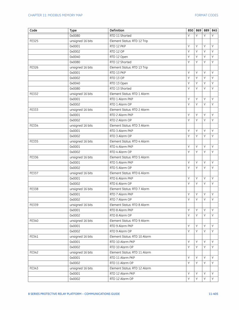
CHAPTER 11: MODBUS MEMORY MAP FORMAT CODES
0x0080 RTD 11 Shorted Y Y Y Y
FE325 unsigned 16 bits Element Status: RTD 12 Trip
0x0001 RTD 12 PKP Y Y Y Y
0x0002 RTD 12 OP Y Y Y Y
0x0040 RTD 12 Open Y Y Y Y
0x0080 RTD 12 Shorted Y Y Y Y
FE326 unsigned 16 bits Element Status: RTD 13 Trip
0x0001 RTD 13 PKP Y Y Y Y
0x0002 RTD 13 OP Y Y Y Y
0x0040 RTD 13 Open Y Y Y Y
0x0080 RTD 13 Shorted Y Y Y Y
FE332 unsigned 16 bits Element Status: RTD 1 Alarm
0x0001 RTD 1 Alarm PKP Y Y Y Y
0x0002 RTD 1 Alarm OP Y Y Y Y
FE333 unsigned 16 bits Element Status: RTD 2 Alarm
0x0001 RTD 2 Alarm PKP Y Y Y Y
0x0002 RTD 2 Alarm OP Y Y Y Y
FE334 unsigned 16 bits Element Status: RTD 3 Alarm
0x0001 RTD 3 Alarm PKP Y Y Y Y
0x0002 RTD 3 Alarm OP Y Y Y Y
FE335 unsigned 16 bits Element Status: RTD 4 Alarm
0x0001 RTD 4 Alarm PKP Y Y Y Y
0x0002 RTD 4 Alarm OP Y Y Y Y
FE336 unsigned 16 bits Element Status: RTD 5 Alarm
0x0001 RTD 5 Alarm PKP Y Y Y Y
0x0002 RTD 5 Alarm OP Y Y Y Y
FE337 unsigned 16 bits Element Status: RTD 6 Alarm
0x0001 RTD 6 Alarm PKP Y Y Y Y
0x0002 RTD 6 Alarm OP Y Y Y Y
FE338 unsigned 16 bits Element Status: RTD 7 Alarm
0x0001 RTD 7 Alarm PKP Y Y Y Y
0x0002 RTD 7 Alarm OP Y Y Y Y
FE339 unsigned 16 bits Element Status: RTD 8 Alarm
0x0001 RTD 8 Alarm PKP Y Y Y Y
0x0002 RTD 8 Alarm OP Y Y Y Y
FE340 unsigned 16 bits Element Status: RTD 9 Alarm
0x0001 RTD 9 Alarm PKP Y Y Y Y
0x0002 RTD 9 Alarm OP Y Y Y Y
FE341 unsigned 16 bits Element Status: RTD 10 Alarm
0x0001 RTD 10 Alarm PKP Y Y Y Y
0x0002 RTD 10 Alarm OP Y Y Y Y
FE342 unsigned 16 bits Element Status: RTD 11 Alarm
0x0001 RTD 11 Alarm PKP Y Y Y Y
0x0002 RTD 11 Alarm OP Y Y Y Y
FE343 unsigned 16 bits Element Status: RTD 12 Alarm
0x0001 RTD 12 Alarm PKP Y Y Y Y
0x0002 RTD 12 Alarm OP Y Y Y Y
Code Type Definition 850 869 889 845
8 SERIES PROTECTIVE RELAY PLATFORM – COMMUNICATIONS GUIDE 11-405
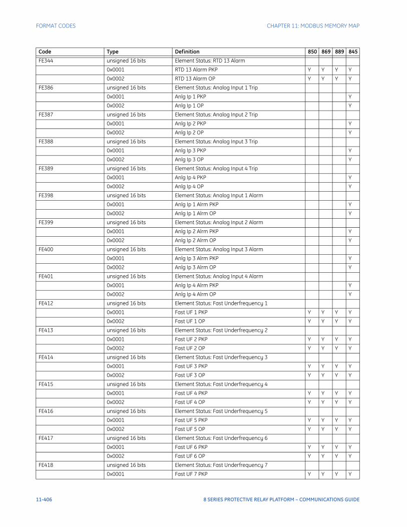
FORMAT CODES CHAPTER 11: MODBUS MEMORY MAP
FE344 unsigned 16 bits Element Status: RTD 13 Alarm
0x0001 RTD 13 Alarm PKP Y Y Y Y
0x0002 RTD 13 Alarm OP Y Y Y Y
FE386 unsigned 16 bits Element Status: Analog Input 1 Trip
0x0001 Anlg Ip 1 PKP Y
0x0002 Anlg Ip 1 OP Y
FE387 unsigned 16 bits Element Status: Analog Input 2 Trip
0x0001 Anlg Ip 2 PKP Y
0x0002 Anlg Ip 2 OP Y
FE388 unsigned 16 bits Element Status: Analog Input 3 Trip
0x0001 Anlg Ip 3 PKP Y
0x0002 Anlg Ip 3 OP Y
FE389 unsigned 16 bits Element Status: Analog Input 4 Trip
0x0001 Anlg Ip 4 PKP Y
0x0002 Anlg Ip 4 OP Y
FE398 unsigned 16 bits Element Status: Analog Input 1 Alarm
0x0001 Anlg Ip 1 Alrm PKP Y
0x0002 Anlg Ip 1 Alrm OP Y
FE399 unsigned 16 bits Element Status: Analog Input 2 Alarm
0x0001 Anlg Ip 2 Alrm PKP Y
0x0002 Anlg Ip 2 Alrm OP Y
FE400 unsigned 16 bits Element Status: Analog Input 3 Alarm
0x0001 Anlg Ip 3 Alrm PKP Y
0x0002 Anlg Ip 3 Alrm OP Y
FE401 unsigned 16 bits Element Status: Analog Input 4 Alarm
0x0001 Anlg Ip 4 Alrm PKP Y
0x0002 Anlg Ip 4 Alrm OP Y
FE412 unsigned 16 bits Element Status: Fast Underfrequency 1
0x0001 Fast UF 1 PKP Y Y Y Y
0x0002 Fast UF 1 OP Y Y Y Y
FE413 unsigned 16 bits Element Status: Fast Underfrequency 2
0x0001 Fast UF 2 PKP Y Y Y Y
0x0002 Fast UF 2 OP Y Y Y Y
FE414 unsigned 16 bits Element Status: Fast Underfrequency 3
0x0001 Fast UF 3 PKP Y Y Y Y
0x0002 Fast UF 3 OP Y Y Y Y
FE415 unsigned 16 bits Element Status: Fast Underfrequency 4
0x0001 Fast UF 4 PKP Y Y Y Y
0x0002 Fast UF 4 OP Y Y Y Y
FE416 unsigned 16 bits Element Status: Fast Underfrequency 5
0x0001 Fast UF 5 PKP Y Y Y Y
0x0002 Fast UF 5 OP Y Y Y Y
FE417 unsigned 16 bits Element Status: Fast Underfrequency 6
0x0001 Fast UF 6 PKP Y Y Y Y
0x0002 Fast UF 6 OP Y Y Y Y
FE418 unsigned 16 bits Element Status: Fast Underfrequency 7
0x0001 Fast UF 7 PKP Y Y Y Y
Code Type Definition 850 869 889 845
11-406 8 SERIES PROTECTIVE RELAY PLATFORM – COMMUNICATIONS GUIDE
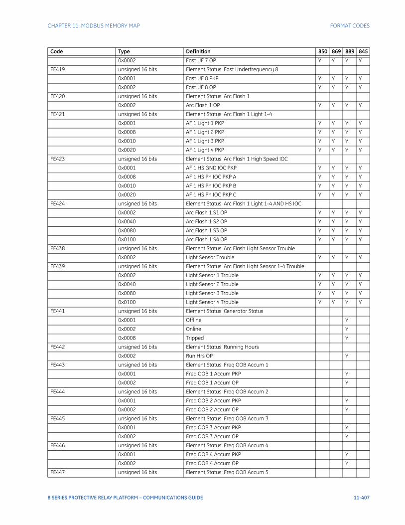
CHAPTER 11: MODBUS MEMORY MAP FORMAT CODES
0x0002 Fast UF 7 OP Y Y Y Y
FE419 unsigned 16 bits Element Status: Fast Underfrequency 8
0x0001 Fast UF 8 PKP Y Y Y Y
0x0002 Fast UF 8 OP Y Y Y Y
FE420 unsigned 16 bits Element Status: Arc Flash 1
0x0002 Arc Flash 1 OP Y Y Y Y
FE421 unsigned 16 bits Element Status: Arc Flash 1 Light 1-4
0x0001 AF 1 Light 1 PKP Y Y Y Y
0x0008 AF 1 Light 2 PKP Y Y Y Y
0x0010 AF 1 Light 3 PKP Y Y Y Y
0x0020 AF 1 Light 4 PKP Y Y Y Y
FE423 unsigned 16 bits Element Status: Arc Flash 1 High Speed IOC
0x0001 AF 1 HS GND IOC PKP Y Y Y Y
0x0008 AF 1 HS Ph IOC PKP A Y Y Y Y
0x0010 AF 1 HS Ph IOC PKP B Y Y Y Y
0x0020 AF 1 HS Ph IOC PKP C Y Y Y Y
FE424 unsigned 16 bits Element Status: Arc Flash 1 Light 1-4 AND HS IOC
0x0002 Arc Flash 1 S1 OP Y Y Y Y
0x0040 Arc Flash 1 S2 OP Y Y Y Y
0x0080 Arc Flash 1 S3 OP Y Y Y Y
0x0100 Arc Flash 1 S4 OP Y Y Y Y
FE438 unsigned 16 bits Element Status: Arc Flash Light Sensor Trouble
0x0002 Light Sensor Trouble Y Y Y Y
FE439 unsigned 16 bits Element Status: Arc Flash Light Sensor 1-4 Trouble
0x0002 Light Sensor 1 Trouble Y Y Y Y
0x0040 Light Sensor 2 Trouble Y Y Y Y
0x0080 Light Sensor 3 Trouble Y Y Y Y
0x0100 Light Sensor 4 Trouble Y Y Y Y
FE441 unsigned 16 bits Element Status: Generator Status
0x0001 Offline Y
0x0002 Online Y
0x0008 Tripped Y
FE442 unsigned 16 bits Element Status: Running Hours
0x0002 Run Hrs OP Y
FE443 unsigned 16 bits Element Status: Freq OOB Accum 1
0x0001 Freq OOB 1 Accum PKP Y
0x0002 Freq OOB 1 Accum OP Y
FE444 unsigned 16 bits Element Status: Freq OOB Accum 2
0x0001 Freq OOB 2 Accum PKP Y
0x0002 Freq OOB 2 Accum OP Y
FE445 unsigned 16 bits Element Status: Freq OOB Accum 3
0x0001 Freq OOB 3 Accum PKP Y
0x0002 Freq OOB 3 Accum OP Y
FE446 unsigned 16 bits Element Status: Freq OOB Accum 4
0x0001 Freq OOB 4 Accum PKP Y
0x0002 Freq OOB 4 Accum OP Y
FE447 unsigned 16 bits Element Status: Freq OOB Accum 5
Code Type Definition 850 869 889 845
8 SERIES PROTECTIVE RELAY PLATFORM – COMMUNICATIONS GUIDE 11-407
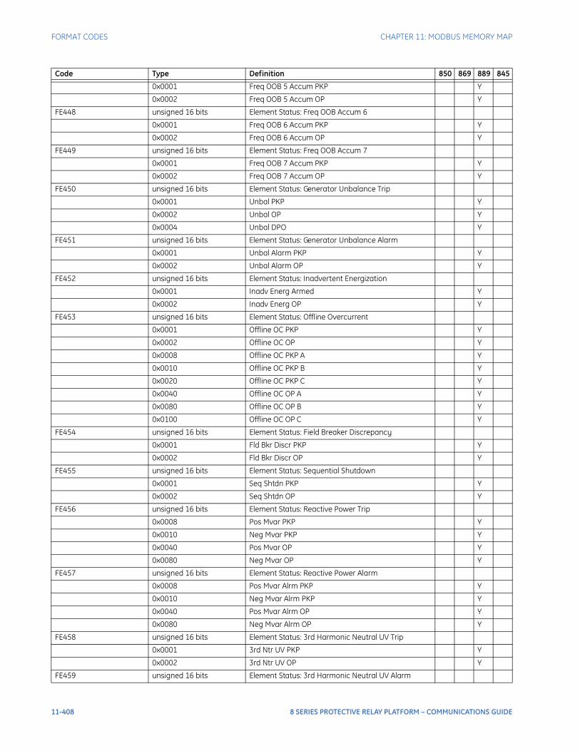
FORMAT CODES CHAPTER 11: MODBUS MEMORY MAP
0x0001 Freq OOB 5 Accum PKP Y
0x0002 Freq OOB 5 Accum OP Y
FE448 unsigned 16 bits Element Status: Freq OOB Accum 6
0x0001 Freq OOB 6 Accum PKP Y
0x0002 Freq OOB 6 Accum OP Y
FE449 unsigned 16 bits Element Status: Freq OOB Accum 7
0x0001 Freq OOB 7 Accum PKP Y
0x0002 Freq OOB 7 Accum OP Y
FE450 unsigned 16 bits Element Status: Generator Unbalance Trip
0x0001 Unbal PKP Y
0x0002 Unbal OP Y
0x0004 Unbal DPO Y
FE451 unsigned 16 bits Element Status: Generator Unbalance Alarm
0x0001 Unbal Alarm PKP Y
0x0002 Unbal Alarm OP Y
FE452 unsigned 16 bits Element Status: Inadvertent Energization
0x0001 Inadv Energ Armed Y
0x0002 Inadv Energ OP Y
FE453 unsigned 16 bits Element Status: Offline Overcurrent
0x0001 Offline OC PKP Y
0x0002 Offline OC OP Y
0x0008 Offline OC PKP A Y
0x0010 Offline OC PKP B Y
0x0020 Offline OC PKP C Y
0x0040 Offline OC OP A Y
0x0080 Offline OC OP B Y
0x0100 Offline OC OP C Y
FE454 unsigned 16 bits Element Status: Field Breaker Discrepancy
0x0001 Fld Bkr Discr PKP Y
0x0002 Fld Bkr Discr OP Y
FE455 unsigned 16 bits Element Status: Sequential Shutdown
0x0001 Seq Shtdn PKP Y
0x0002 Seq Shtdn OP Y
FE456 unsigned 16 bits Element Status: Reactive Power Trip
0x0008 Pos Mvar PKP Y
0x0010 Neg Mvar PKP Y
0x0040 Pos Mvar OP Y
0x0080 Neg Mvar OP Y
FE457 unsigned 16 bits Element Status: Reactive Power Alarm
0x0008 Pos Mvar Alrm PKP Y
0x0010 Neg Mvar Alrm PKP Y
0x0040 Pos Mvar Alrm OP Y
0x0080 Neg Mvar Alrm OP Y
FE458 unsigned 16 bits Element Status: 3rd Harmonic Neutral UV Trip
0x0001 3rd Ntr UV PKP Y
0x0002 3rd Ntr UV OP Y
FE459 unsigned 16 bits Element Status: 3rd Harmonic Neutral UV Alarm
Code Type Definition 850 869 889 845
11-408 8 SERIES PROTECTIVE RELAY PLATFORM – COMMUNICATIONS GUIDE
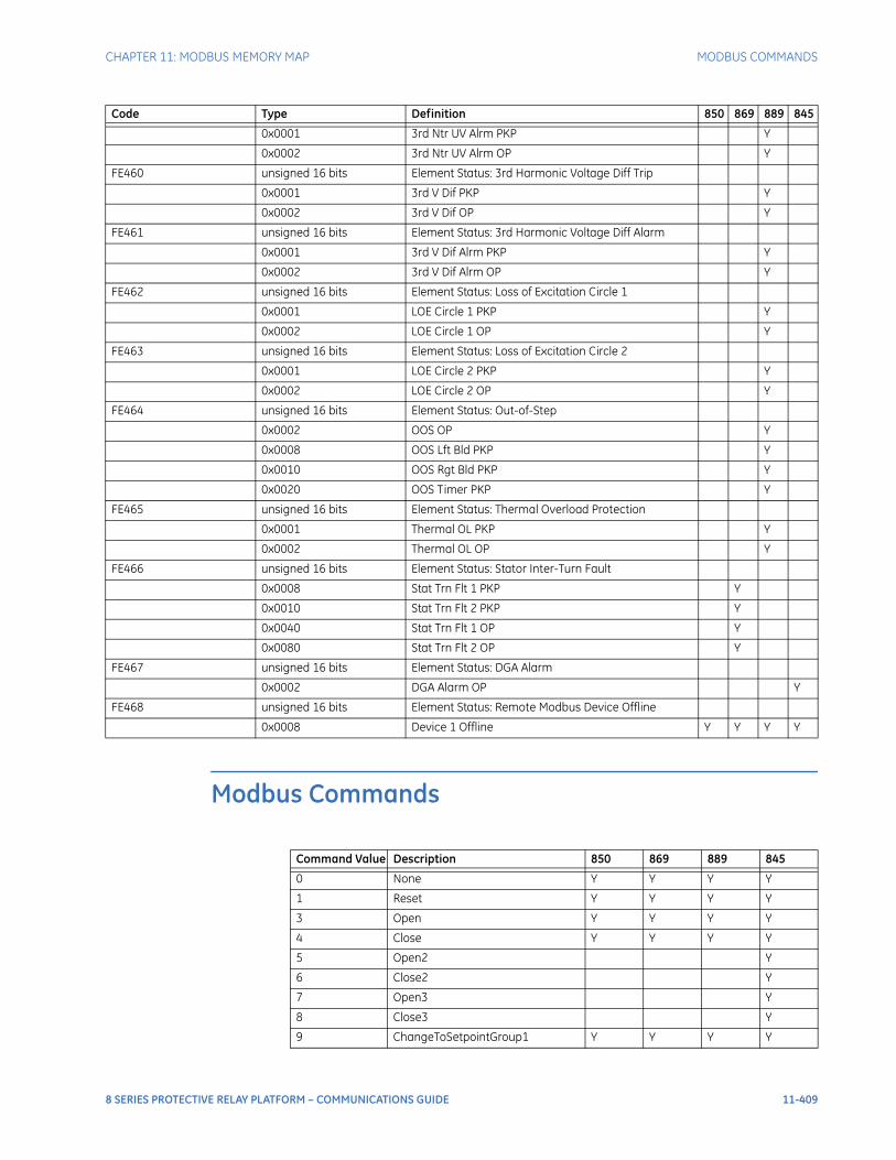
CHAPTER 11: MODBUS MEMORY MAP MODBUS COMMANDS
Modbus Commands
0x0001 3rd Ntr UV Alrm PKP Y
0x0002 3rd Ntr UV Alrm OP Y
FE460 unsigned 16 bits Element Status: 3rd Harmonic Voltage Diff Trip
0x0001 3rd V Dif PKP Y
0x0002 3rd V Dif OP Y
FE461 unsigned 16 bits Element Status: 3rd Harmonic Voltage Diff Alarm
0x0001 3rd V Dif Alrm PKP Y
0x0002 3rd V Dif Alrm OP Y
FE462 unsigned 16 bits Element Status: Loss of Excitation Circle 1
0x0001 LOE Circle 1 PKP Y
0x0002 LOE Circle 1 OP Y
FE463 unsigned 16 bits Element Status: Loss of Excitation Circle 2
0x0001 LOE Circle 2 PKP Y
0x0002 LOE Circle 2 OP Y
FE464 unsigned 16 bits Element Status: Out-of-Step
0x0002 OOS OP Y
0x0008 OOS Lft Bld PKP Y
0x0010 OOS Rgt Bld PKP Y
0x0020 OOS Timer PKP Y
FE465 unsigned 16 bits Element Status: Thermal Overload Protection
0x0001 Thermal OL PKP Y
0x0002 Thermal OL OP Y
FE466 unsigned 16 bits Element Status: Stator Inter-Turn Fault
0x0008 Stat Trn Flt 1 PKP Y
0x0010 Stat Trn Flt 2 PKP Y
0x0040 Stat Trn Flt 1 OP Y
0x0080 Stat Trn Flt 2 OP Y
FE467 unsigned 16 bits Element Status: DGA Alarm
0x0002 DGA Alarm OP Y
FE468 unsigned 16 bits Element Status: Remote Modbus Device Offline
0x0008 Device 1 Offline Y Y Y Y
Code Type Definition 850 869 889 845
Command Value Description 850 869 889 845
0 None Y Y Y Y
1 Reset Y Y Y Y
3 Open Y Y Y Y
4 Close Y Y Y Y
5 Open2 Y
6 Close2 Y
7 Open3 Y
8 Close3 Y
9 ChangeToSetpointGroup1 Y Y Y Y
8 SERIES PROTECTIVE RELAY PLATFORM – COMMUNICATIONS GUIDE 11-409
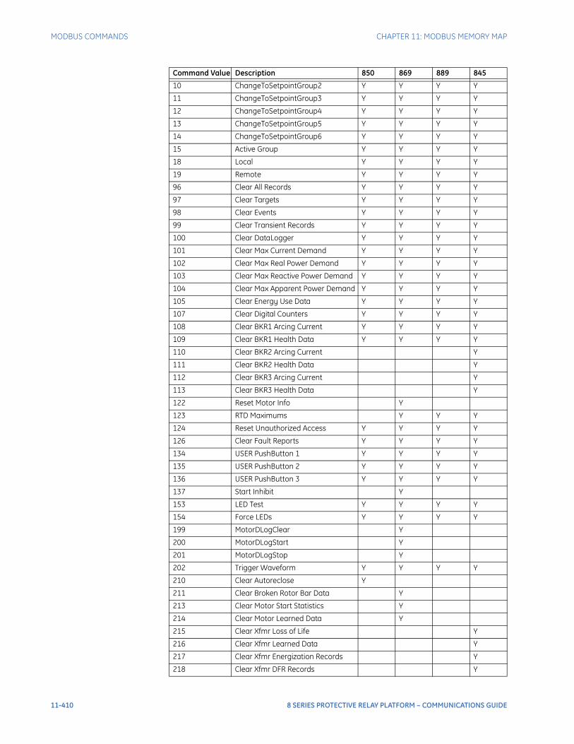
MODBUS COMMANDS CHAPTER 11: MODBUS MEMORY MAP
10 ChangeToSetpointGroup2 Y Y Y Y
11 ChangeToSetpointGroup3 Y Y Y Y
12 ChangeToSetpointGroup4 Y Y Y Y
13 ChangeToSetpointGroup5 Y Y Y Y
14 ChangeToSetpointGroup6 Y Y Y Y
15 Active Group Y Y Y Y
18 Local Y Y Y Y
19 Remote Y Y Y Y
96 Clear All Records Y Y Y Y
97 Clear Targets Y Y Y Y
98 Clear Events Y Y Y Y
99 Clear Transient Records Y Y Y Y
100 Clear DataLogger Y Y Y Y
101 Clear Max Current Demand Y Y Y Y
102 Clear Max Real Power Demand Y Y Y Y
103 Clear Max Reactive Power Demand Y Y Y Y
104 Clear Max Apparent Power Demand Y Y Y Y
105 Clear Energy Use Data Y Y Y Y
107 Clear Digital Counters Y Y Y Y
108 Clear BKR1 Arcing Current Y Y Y Y
109 Clear BKR1 Health Data Y Y Y Y
110 Clear BKR2 Arcing Current Y
111 Clear BKR2 Health Data Y
112 Clear BKR3 Arcing Current Y
113 Clear BKR3 Health Data Y
122 Reset Motor Info Y
123 RTD Maximums Y Y Y
124 Reset Unauthorized Access Y Y Y Y
126 Clear Fault Reports Y Y Y Y
134 USER PushButton 1 Y Y Y Y
135 USER PushButton 2 Y Y Y Y
136 USER PushButton 3 Y Y Y Y
137 Start Inhibit Y
153 LED Test Y Y Y Y
154 Force LEDs Y Y Y Y
199 MotorDLogClear Y
200 MotorDLogStart Y
201 MotorDLogStop Y
202 Trigger Waveform Y Y Y Y
210 Clear Autoreclose Y
211 Clear Broken Rotor Bar Data Y
213 Clear Motor Start Statistics Y
214 Clear Motor Learned Data Y
215 Clear Xfmr Loss of Life Y
216 Clear Xfmr Learned Data Y
217 Clear Xfmr Energization Records Y
218 Clear Xfmr DFR Records Y
Command Value Description 850 869 889 845
11-410 8 SERIES PROTECTIVE RELAY PLATFORM – COMMUNICATIONS GUIDE
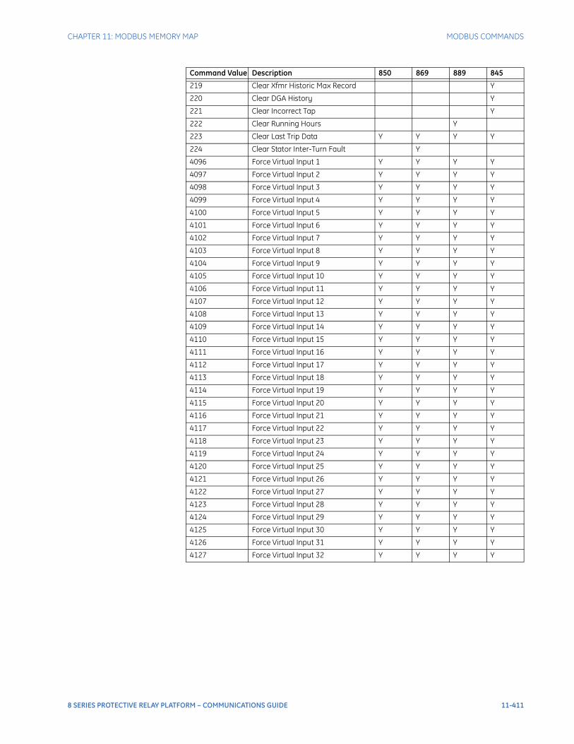
CHAPTER 11: MODBUS MEMORY MAP MODBUS COMMANDS
219 Clear Xfmr Historic Max Record Y
220 Clear DGA History Y
221 Clear Incorrect Tap Y
222 Clear Running Hours Y
223 Clear Last Trip Data Y Y Y Y
224 Clear Stator Inter-Turn Fault Y
4096 Force Virtual Input 1 Y Y Y Y
4097 Force Virtual Input 2 Y Y Y Y
4098 Force Virtual Input 3 Y Y Y Y
4099 Force Virtual Input 4 Y Y Y Y
4100 Force Virtual Input 5 Y Y Y Y
4101 Force Virtual Input 6 Y Y Y Y
4102 Force Virtual Input 7 Y Y Y Y
4103 Force Virtual Input 8 Y Y Y Y
4104 Force Virtual Input 9 Y Y Y Y
4105 Force Virtual Input 10 Y Y Y Y
4106 Force Virtual Input 11 Y Y Y Y
4107 Force Virtual Input 12 Y Y Y Y
4108 Force Virtual Input 13 Y Y Y Y
4109 Force Virtual Input 14 Y Y Y Y
4110 Force Virtual Input 15 Y Y Y Y
4111 Force Virtual Input 16 Y Y Y Y
4112 Force Virtual Input 17 Y Y Y Y
4113 Force Virtual Input 18 Y Y Y Y
4114 Force Virtual Input 19 Y Y Y Y
4115 Force Virtual Input 20 Y Y Y Y
4116 Force Virtual Input 21 Y Y Y Y
4117 Force Virtual Input 22 Y Y Y Y
4118 Force Virtual Input 23 Y Y Y Y
4119 Force Virtual Input 24 Y Y Y Y
4120 Force Virtual Input 25 Y Y Y Y
4121 Force Virtual Input 26 Y Y Y Y
4122 Force Virtual Input 27 Y Y Y Y
4123 Force Virtual Input 28 Y Y Y Y
4124 Force Virtual Input 29 Y Y Y Y
4125 Force Virtual Input 30 Y Y Y Y
4126 Force Virtual Input 31 Y Y Y Y
4127 Force Virtual Input 32 Y Y Y Y
Command Value Description 850 869 889 845
8 SERIES PROTECTIVE RELAY PLATFORM – COMMUNICATIONS GUIDE 11-411

MODBUS COMMANDS CHAPTER 11: MODBUS MEMORY MAP
11-412 8 SERIES PROTECTIVE RELAY PLATFORM – COMMUNICATIONS GUIDE

8 Series Protective Relay Platform
Appendix A: 845 Radius Server and Certificates
GEGrid Solutions
845 Radius Server and Certif icates
Appendix A includes information about the RADIUS server and certificates followed by an example of how to set up a simple RADIUS server and certificate management.
Simple RADIUS Server and Certificate Management
The 8 Series unit can act as a RADIUS client and has the ability to authenticate users with a RADIUS server using the EAP-TTLS protocol. Authentication is performed with the help of certificates.Any cryptography application such as OpenSSL etc. can be used to create certificates. First, a private key and certificate request are created for the server. The certificate request contains the public key, and the server’s information (name, email, organization etc.) The certificate request is then sent to a certificate authority (CA) for the authority’s digital signature. If the request is sent to a well-known CA, then upon receiving payment from the RADIUS server’s administrator, the CA verifies the information and signs the certificate. The administrator can choose not to use an external well-known CA’s services and create a local CA instead.The signed certificate of the server along with CA’s public certificate are then sent back to the RADIUS server administrator. Finally, the CA’s public certificate is uploaded to the relay.In this example, a local CA is created and used to sign the server’s certificate request.
Create a CA and Server Certificates -->
Transfer the server’s private- public certificate pairand the CA’s public certificate to the RADIUS server
-->Upload the CA’s public certificate to the 8 Series unit
8 SERIES PROTECTIVE RELAY PLATFORM – COMMUNICATIONS GUIDE A-A-1

SETTING UP A SIMPLE RADIUS SERVER CHAPTER A: 845 RADIUS SERVER AND CERTIFICATES
Authentication:The user initiates the authentication process by providing user credentials. The 8 Series unit then tries to establish a trust relationship with the RADIUS server. The RADIUS server identifies itself via a certificate which it sends to the 8 Series unit. This certificate holds the server’s information:
• version
• public key
• subject
• serial number
• valid from
• valid until
• key-usage
• signature algorithm
• “issuer” (i.e. CA) etc.
The 8 Series unit then validates the server’s identity by verifying the server’s certificate against the CA certificate that it has. If both the server and CA certificates are signed by the same trusted authority (CA), a client side trust relationship is successfully established.
Setting Up a Simple RADIUS Server
The following example demonstrates how to set up a test bench RADIUS server. A proper RADIUS server is only to be deployed by qualified IT professionals. The third party tools and services mentioned below are only for demonstration purposes and do not imply endorsement by GE.This example uses FreeRADIUS as the RADIUS server.Download and install FreeRADIUS.net (Windows™ version) from the following location: http://freeradius.net/
Radius Server Certificate ManagementThe activities described here are required for certificate management.
Create a Private Key for the Server
To create a private key by using the command:
openssl genrsa –out server.key 4096
The RSA based private key is generated.
NOTE
The RSA based private key is not a password protected key.
Create a Certificate Request for the Server
To create a certificate request by using the command:
openssl req –new –key server.key –out server.csr
While using the command, you are asked to enter the following information that is incorporated into the certificate request.
• Country Name
• State or Province Name
A-A-2 8 SERIES PROTECTIVE RELAY PLATFORM – COMMUNICATIONS GUIDE
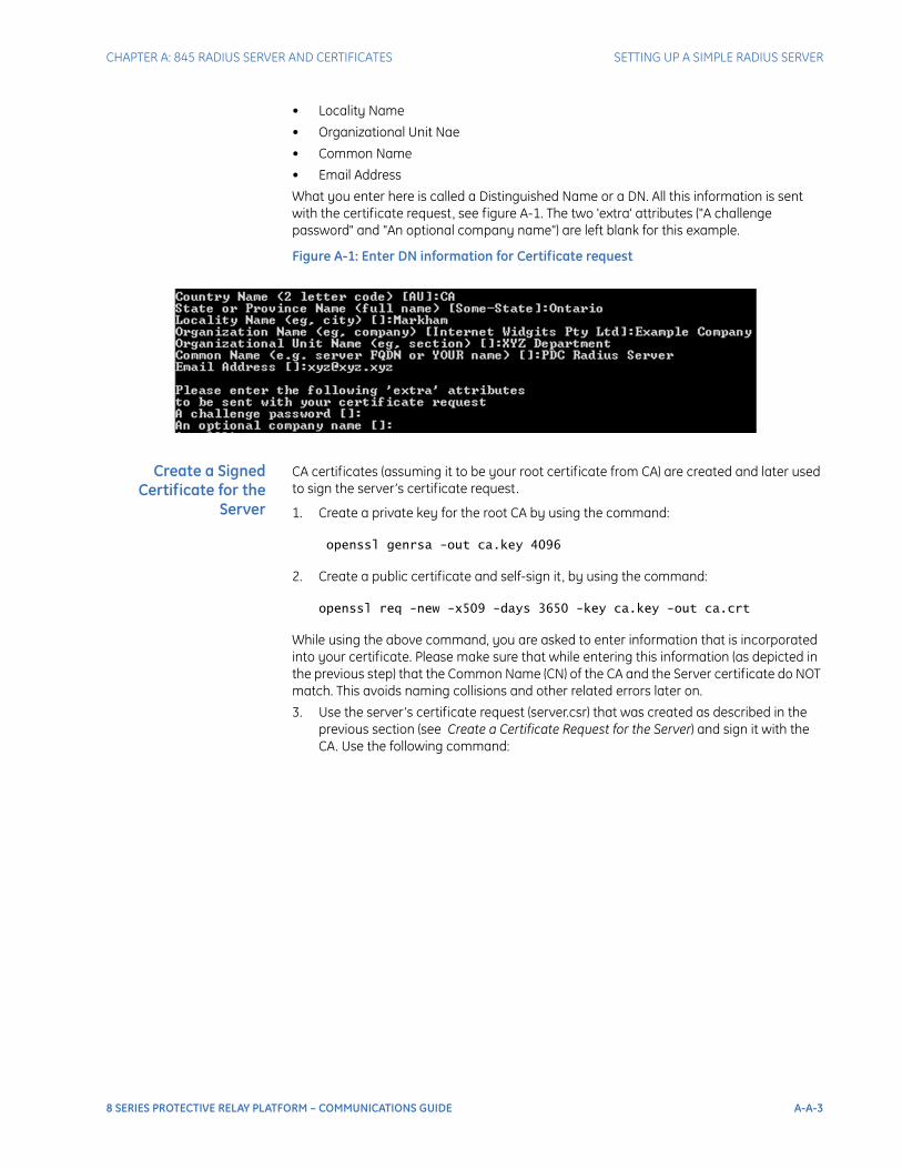
CHAPTER A: 845 RADIUS SERVER AND CERTIFICATES SETTING UP A SIMPLE RADIUS SERVER
• Locality Name
• Organizational Unit Nae
• Common Name
• Email Address
What you enter here is called a Distinguished Name or a DN. All this information is sent with the certificate request, see figure A-1. The two 'extra' attributes ("A challenge password" and "An optional company name") are left blank for this example.
Figure A-1: Enter DN information for Certificate request
Create a Signed Certificate for the
Server
CA certificates (assuming it to be your root certificate from CA) are created and later used to sign the server’s certificate request.
1. Create a private key for the root CA by using the command:
openssl genrsa -out ca.key 4096
2. Create a public certificate and self-sign it , by using the command:
openssl req -new -x509 -days 3650 -key ca.key -out ca.crt
While using the above command, you are asked to enter information that is incorporated into your certificate. Please make sure that while entering this information (as depicted in the previous step) that the Common Name (CN) of the CA and the Server certificate do NOT match. This avoids naming collisions and other related errors later on.
3. Use the server’s certificate request (server.csr) that was created as described in the previous section (see Create a Certificate Request for the Server) and sign it with the CA. Use the following command:
8 SERIES PROTECTIVE RELAY PLATFORM – COMMUNICATIONS GUIDE A-A-3
SETTING UP A SIMPLE RADIUS SERVER CHAPTER A: 845 RADIUS SERVER AND CERTIFICATES
d d
lf-
a
t
openssl x509 –req –days 3650 –in server.csr –CA ca.crt –CAkey ca.key –set_serial 01 –out server.crt
Transfer Certificates to ServerCopy the following files,
• server.key
• server.crt
• ca.crt
onto the FreeRADIUS.net server under the directory containing the certificates.In this example the directory is located under the path: <Path_to_Radius>\etc\raddb\certs\FreeRADIUS.net\DemoCerts>
Radius Server ConfigurationModify the following .GE and .CONF files to configure the RADIUS server.RADIUSD.CONFLocate the “bind_address” field and set it to your RADIUS server’s IP address in the radiusd.conf file.USERS.CONFAdd the users in the users.conf file.The file is available under the <Path_to_Radius>\etc\raddb directory.Adding the following text configures a user “Tester” which has an “Administrator” role.
Tester:
->User-Password == “Testing1!1”
->GE-UR-Role = Administrator
CLIENTS.CONFAdd the clients in the clients.conf file.The file is available under the <Path_to_Radius>\etc\raddb directory.
Definitions
x509 This term is used to add a digital signature to the certificate.
-req With this option, a certificate request is expected instead of the certificate (by default).
-in Specifies the input file from which the certificate is read.
-CA
Specifies the CA certificate to be used for signing.When the -CA option is present, x509 behaves like a “mini CA”. The input file is signeby this CA using this option. The issuer name is set to the subject name of the CA anit is digitally signed using the CA’s private key. This option is normally combined withthe –req option. Without the –req option, the input is a certificate which must be sesigned.
-CAkey
When the -CA option is used to sign a certificate, it uses a serial number specified infile. This file consists of one line containing an even number of hex digits with the serial number to use. After each use, the serial number is incremented and written outo the file again.
-set_serial Specifies the serial number to use.
-out Specifies the output file to write to.
–days Specifies the number of days the certificate is valid.
A-A-4 8 SERIES PROTECTIVE RELAY PLATFORM – COMMUNICATIONS GUIDE
CHAPTER A: 845 RADIUS SERVER AND CERTIFICATES SETTING UP A SIMPLE RADIUS SERVER
The following text defines a RADIUS client 8 Series unit with the assumption that its IP-address is 10.0.0.2 and subnet mask is 255.255.255.0. The “secret” that is specified here is also configured on the 8 Series unit for successful authentication. The “shortname” is a short alias that can be used in place of the IP address and it is optional.
client 10.0.0.2/24 {
secret = testing123
shortname = private-network-1
}
DICTIONARY.GECreate a file called “dictionary.ge” under the <Path_to_Radius>\etc\raddb directory and add the following content to it:
# ##########################################################
# GE VSA’s
############################################################
VENDOR GE 2910
# Management authorization
BEGIN-VENDOR GE
# Role ID
ATTRIBUTE GE-UR-Role 1 integer
# GE-UR-ROLE values
VALUE GE-UR-Role Administrator 1
VALUE GE-UR-Role Supervisor 2
VALUE GE-UR-Role Engineer 3
VALUE GE-UR-Role Operator 4
VALUE GE-UR-Role Observer 5
END-VENDOR GE
#############################################################
DICTIONARY
Add the following line to the “dictionary” file present under <Path_to_Radius>\etc\raddb.
$INCLUDE dictionary.ge
EAP.CONFThe eap.conf file is available under the <Path_to_Radius>\etc\raddb directory.Locate the “tls” block and add the respective entries as shown in figure A-2 to the “private_key_file”, ”certificate_file” and “CA_file” fields.
8 SERIES PROTECTIVE RELAY PLATFORM – COMMUNICATIONS GUIDE A-A-5
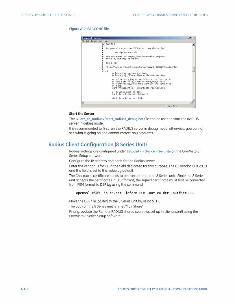
SETTING UP A SIMPLE RADIUS SERVER CHAPTER A: 845 RADIUS SERVER AND CERTIFICATES
Figure A-2: EAP.CONF file
Start the ServerThe <Path_to_Radius>/start_radiusd_debug.bat file can be used to start the RADIUS server in debug mode.It is recommended to first run the RADIUS server in debug mode, otherwise, you cannot see what is going on and cannot correct any problems.
Radius Client Configuration (8 Series Unit)Radius settings are configured under Setpoints > Device > Security on the EnerVista 8 Series Setup software.Configure the IP address and ports for the Radius server.Enter the vendor ID for GE in the field dedicated for this purpose. The GE vendor ID is 2910 and the field is set to this value by default.The CA’s public certificate needs to be transferred to the 8 Series unit . Since the 8 Series unit accepts the certificates in DER format, the signed certificate must first be converted from PEM format to DER by using the command:
openssl x509 -in ca.crt -inform PEM -out ca.der -outform DER
Move the DER file (ca.der) to the 8 Series unit by using SFTP.The path on the 8 Series unit is “/net/MainShare”Finally, update the Remote RADIUS shared secret (as set up in clients.conf) using the EnerVista 8 Series Setup software.
A-A-6 8 SERIES PROTECTIVE RELAY PLATFORM – COMMUNICATIONS GUIDE
8 Series Protective Relay Platform
Appendix B: Warranty and Revision History
GEGrid Solutions
Warranty and Revision History
This Appendix includes the warranty and revision history.
Warranty
For products shipped as of 1 October 2013, GE warrants most of its GE manufactured products for 10 years. For warranty details including any limitations and disclaimers, see our Terms and Conditions at https://www.gegridsolutions.com/multilin/warranty.htmFor products shipped before 1 October 2013, the standard 24-month warranty applies.
Revision history
Major Updates
Table B-1: Revision History
MANUAL P/N RELEASE DATE
1601-0702-A1 March 2016
1601-0702-A2 April 2016
Table B-2: Major Updates for 8 Series Communications A2
PAGE NUMBER CHANGES
Chapter 11 Modbus Map updated
8 SERIES PROTECTIVE RELAY PLATFORM – COMMUNICATIONS GUIDE B-B-1

REVISION HISTORY CHAPTER B: WARRANTY AND REVISION HISTORY
NOTE
This manual replaces the following individual product Communications Guides:
• 850 Feeder Protection System Communications Guide (1601-0299-A5)
• 845 Transformer Protection System Communications Guide (1601-0409-A2)
• 869 Motor Protection System Communications Guide (1601-0451-A3)
Table B-3: Major Updates for 8 Series Communications A1
PAGE NUMBER CHANGES
Initial release of combined 8 Series Communications Guide