Project Design Guide (Phase-Locked Loop) - Yonsei...
16
High-Speed Circuits & Systems Lab. Dept. of Electrical and Electronic Engineering Yonsei University Project Design Guide (Phase-Locked Loop)
Transcript of Project Design Guide (Phase-Locked Loop) - Yonsei...

High-Speed Circuits & Systems Lab.
Dept. of Electrical and Electronic Engineering
Yonsei University
Project Design Guide(Phase-Locked Loop)

2 page / 16 page
Goals
Full PLL simulation-PFD, Divider: Verilog-A model-Charge pump, Loop filter, VCO: schematic model
Loop bandwidth optimization-Low-jitter PLL can be achieved
PFDLoop
Filter
LC VCO
Divider
(÷16)
Charge
Pump
Ref.
clockOutput
clock
Schematic designed
3 page / 16 page
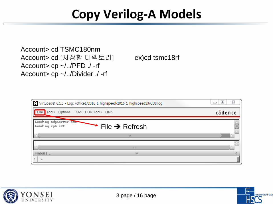
Copy Verilog-A Models
Account> cd TSMC180nm
Account> cd [저장할디렉토리] ex)cd tsmc18rf
Account> cp ~/../PFD ./ -rf
Account> cp ~/../Divider ./ -rf
File Refresh

4 page / 16 page
Verilog-A Models
PFD(Phase Frequency Detector)-vin_if: reference clock-vin_lo: feedback clock-sigout_inc: 𝑈𝑃-sigout_dec: Down
ref) www.designers-guide.org
Divider-in: input clock-o: output clock-Threshold: 1.75V-Output swing: 0~1.8V

5 page / 16 page
Create Symbols
Ports

6 page / 16 page
Create Symbols
Same thing for VCO
Use symbols in top level design-PLL design simulation

7 page / 16 page
PLL TOP Schematic
Ref. clock-1.8V swing
(0.9V offset)
-75MHz frequency
Charge-Pump-200uA current
(as designed before)
-0.9V bias
Loop filter-R=5.7k Ohm
-C1=148 pF
-C2=10 pF
LC VCO-1.2GHz target
(as designed before)
-0.8V bias

8 page / 16 page
Reference Clock
Noise-Freq1(Hz)
Noise BW
:10G
-Noise1(V2/Hz)
Noise Magnitude
:1f
Frequency-0.9V offset
-1.8V swing
-75Mhz
White noise f
PSD
(V2/Hz)
fnoise
Noise
BW
Noise
Magnitude

9 page / 16 page
Bias & Terminal
LC VCO(Differential output)
-Add Instance basics
noConnPlace
Bias
-Charge pump bias: 0.9V-VCO bias: 0.8V
Current
Monitor

10 page / 16 page
Simulation Setup(Transient)Time: 20us
Accuracy: conservative(mandatory!!)
Transient noise
-Noise Fmax: 10G
-Noise Fmin: 1K
-Noise Seed:1
-Noise Scale:1
-Noise Tmin:1/Fmax=100p
-Noise Update: fmax
Noise Contribution: on
-Input sine source
-LC VCO
Initial Condition
-LC VCO supply(0V) noise
-Vcont(0V) Step-response

11 page / 16 page
Simulation Result
Vcont
Vout
Output Frequency

12 page / 16 page
Eye Diagram
Eye Diagram

13 page / 16 page
Jitter
Period jitter: ∆ = 𝑇0 − 𝑡𝑖+1′ − 𝑡𝑖
′
Cycle-to-cycle jitter: ∆ = (𝑡𝑖+2′ − 𝑡𝑖+1
′ ) − (𝑡𝑖+1′ − 𝑡𝑖
′)
Absolute jitter: ∆ = 𝑡𝑖 − 𝑡𝑖′ Commonly used
Phase noise
(Frequency domain)
Jitter
(Time domain)
. . .timet0 t1 t2 t3 ti-1 ti
T0
. . .timet0
't1
't2
't3
'ti-1
'ti
'

14 page / 16 page
Loop BW Optimization
Low-pass Filtered High-pass Filtered
Wider BWWider BW

15 page / 16 page
Jitter Measurement(Jabs)
Clip wave from 15us to 20us Calculate jitter with given period
Absolute Jitter
(From 15us to 20us)
Peak-to-peak jitter
-calculator
(peakToPeak)
:34p
RMS jitter
-calculator
(rms)
:16.26ps(0.02UI)

16 page / 16 page
Project
Design 2.5GHz PLL with LC VCO(Input reference noise: 1f V2/Hz PSD, 10GHz BW)
Use schematic level circuits for CP, LF, VCO and Verilog-A models for PFD, Divider-Design each block for better performance(schematic level circuits)
-Recommend to set C2 as C1/15
Show schematic(size), Vcont(transient result), output clock, eye diagram, rms jitter
(minimum 5us interval).
Explain how you come up with your circuit design and loop filter design.
Compare and analyze the step-response of theoretical second-order system(approximation)
and simulation result with your design parameters(ICP, KVCO, R & C).
Due date: 26. Apr (Tue.) 09:30
PFD
LC VCO
Divider
(÷16)
Charge
Pump
Ref.
clock
(156.125MHz)
Output
clock
(2.5GHz)
Loop
Filter
R1
C1
C2
Vcont