PrimeCell High-Performance Matrix (PL301) Technical...
52
Copyright © 2006-2008 ARM Limited. All rights reserved. ARM DDI 0422D PrimeCell ® High-Performance Matrix (PL301) Revision: r1p2 Technical Summary
-
Upload
hoangtuyen -
Category
Documents
-
view
226 -
download
1
Transcript of PrimeCell High-Performance Matrix (PL301) Technical...

PrimeCell® High-Performance Matrix(PL301)Revision: r1p2
Technical Summary
Copyright © 2006-2008 ARM Limited. All rights reserved.ARM DDI 0422D

PrimeCell High-Performance Matrix (PL301)Technical Summary
Copyright © 2006-2008 ARM Limited. All rights reserved.
Release Information
The Change history table lists the changes made to this summary.
Proprietary Notice
Words and logos marked with ® or ™ are registered trademarks or trademarks of ARM Limited in the EU and other countries, except as otherwise stated below in this proprietary notice. Other brands and names mentioned herein may be the trademarks of their respective owners.
Neither the whole nor any part of the information contained in, or the product described in, this document may be adapted or reproduced in any material form except with the prior written permission of the copyright holder.
The product described in this document is subject to continuous developments and improvements. All particulars of the product and its use contained in this document are given by ARM in good faith. However, all warranties implied or expressed, including but not limited to implied warranties of merchantability, or fitness for purpose, are excluded.
This document is intended only to assist the reader in the use of the product. ARM Limited shall not be liable for any loss or damage arising from the use of any information in this document, or any error or omission in such information, or any incorrect use of the product.
Where the term ARM is used it means “ARM or any of its subsidiaries as appropriate”.
Confidentiality Status
This document is Non-Confidential. The right to use, copy and disclose this document may be subject to license restrictions in accordance with the terms of the agreement entered into by ARM and the party that ARM delivered this document to.
Product Status
The information in this document is final, that is for a developed product.
Web Address
http://www.arm.com
Change history
Date Issue Confidentiality Change
21 December 2006 A Non-Confidential First release, but not released externally.
06 July 2007 B Non-Confidential First release for r1p1.
01 October 2007 C Non-Confidential First release for r1p2.
22 April 2008 D Non-Confidential Second release for r1p2. Updated Table 2-1 on page 2-7 and Table 2-2 on page 2-8.
ii Copyright © 2006-2008 ARM Limited. All rights reserved. ARM DDI 0422D

ContentsPrimeCell High-Performance Matrix (PL301) Technical Summary
PrefaceAbout this summary ....................................................................................... xFeedback ..................................................................................................... xiv
Chapter 1 Introduction1.1 About the High-Performance Matrix ............................................................ 1-21.2 Key features ................................................................................................ 1-4
Chapter 2 Programmable Features2.1 Programmable Quality of Service (ProgQoS) ............................................. 2-22.2 Arbitration scheme ...................................................................................... 2-42.3 Summary of SI options ................................................................................ 2-72.4 Summary of MI options ............................................................................... 2-8
Chapter 3 Programmers Model3.1 About the programmers model .................................................................... 3-23.2 Register summary ....................................................................................... 3-33.3 Programmable Quality of Service (ProgQoS) ............................................. 3-43.4 Arbitration control ........................................................................................ 3-63.5 Configuration and ID registers .................................................................. 3-10
ARM DDI 0422D Copyright © 2006-2008 ARM Limited. All rights reserved. iii

Contents
Glossary
iv Copyright © 2006-2008 ARM Limited. All rights reserved. ARM DDI 0422D
List of TablesPrimeCell High-Performance Matrix (PL301) Technical Summary
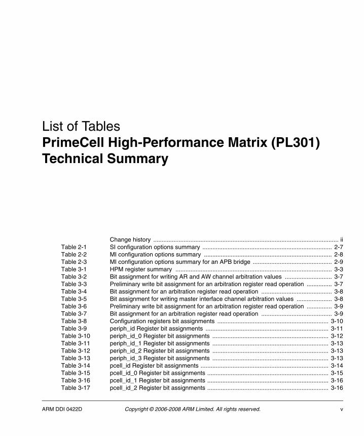
Change history .............................................................................................................. iiTable 2-1 SI configuration options summary ............................................................................. 2-7Table 2-2 MI configuration options summary ............................................................................ 2-8Table 2-3 MI configuration options summary for an APB bridge ............................................... 2-9Table 3-1 HPM register summary ............................................................................................. 3-3Table 3-2 Bit assignment for writing AR and AW channel arbitration values ............................ 3-7Table 3-3 Preliminary write bit assignment for an arbitration register read operation ............... 3-7Table 3-4 Bit assignment for an arbitration register read operation .......................................... 3-8Table 3-5 Bit assignment for writing master interface channel arbitration values ..................... 3-8Table 3-6 Preliminary write bit assignment for an arbitration register read operation ............... 3-9Table 3-7 Bit assignment for an arbitration register read operation .......................................... 3-9Table 3-8 Configuration registers bit assignments .................................................................. 3-10Table 3-9 periph_id Register bit assignments ......................................................................... 3-11Table 3-10 periph_id_0 Register bit assignments ..................................................................... 3-12Table 3-11 periph_id_1 Register bit assignments ..................................................................... 3-13Table 3-12 periph_id_2 Register bit assignments ..................................................................... 3-13Table 3-13 periph_id_3 Register bit assignments ..................................................................... 3-13Table 3-14 pcell_id Register bit assignments ............................................................................ 3-14Table 3-15 pcell_id_0 Register bit assignments ........................................................................ 3-15Table 3-16 pcell_id_1 Register bit assignments ........................................................................ 3-16Table 3-17 pcell_id_2 Register bit assignments ........................................................................ 3-16
ARM DDI 0422D Copyright © 2006-2008 ARM Limited. All rights reserved. v

List of Tables
Table 3-18 pcell_id_3 Register bit assignments ....................................................................... 3-16
vi Copyright © 2006-2008 ARM Limited. All rights reserved. ARM DDI 0422D

List of FiguresPrimeCell High-Performance Matrix (PL301) Technical Summary
Figure 1-1 Example top-level hierarchy ...................................................................................... 1-2Figure 2-1 Example implementation of ProgQoS control registers for 2×1 interconnect ............ 2-2Figure 2-2 Example operation of RR arbitration scheme ........................................................... 2-5Figure 2-3 Example operation of LRG arbitration scheme ......................................................... 2-6Figure 3-1 Configuration registers bit assignments .................................................................. 3-11Figure 3-2 periph_id Register bit assignments ......................................................................... 3-12Figure 3-3 pcell_id Register bit assignments ............................................................................ 3-15
ARM DDI 0422D Copyright © 2006-2008 ARM Limited. All rights reserved. vii

List of Figures
viii Copyright © 2006-2008 ARM Limited. All rights reserved. ARM DDI 0422D

Preface
This preface introduces the AMBA® 3-compliant PrimeCell High-Performance Matrix Technical Summary. It contains the following sections:
• About this summary on page x
• Feedback on page xiv.
ARM DDI 0422D Copyright © 2006-2008 ARM Limited. All rights reserved. ix

Preface
About this summary
This is the Technical Summary (TS) for the PrimeCell High-Performance Matrix (HPM).
Product revision status
The rnpn identifier indicates the revision status of the product described in this summary, where:
rn Identifies the major revision of the product.
pn Identifies the minor revision or modification status of the product.
Intended audience
This summary is written for system designers, system integrators, and programmers who are designing or programming a System-on-Chip (SoC) that uses the HPM.
Using this summary
This summary is organized into the following chapters:
Chapter 1 Introduction
Read this chapter for a high-level view of the HPM and a description of its features.
Chapter 2 Programmable Features
Read this chapter for a description of the controllable HPM characteristics.
Chapter 3 Programmers Model
Read this chapter for a description of:
• the PrimeCell ID registers
• how to program Quality of Service (QoS) and arbitration
• how to read identity and configuration data.
Glossary Read the Glossary for definitions of terms used in this summary.
x Copyright © 2006-2008 ARM Limited. All rights reserved. ARM DDI 0422D
Preface
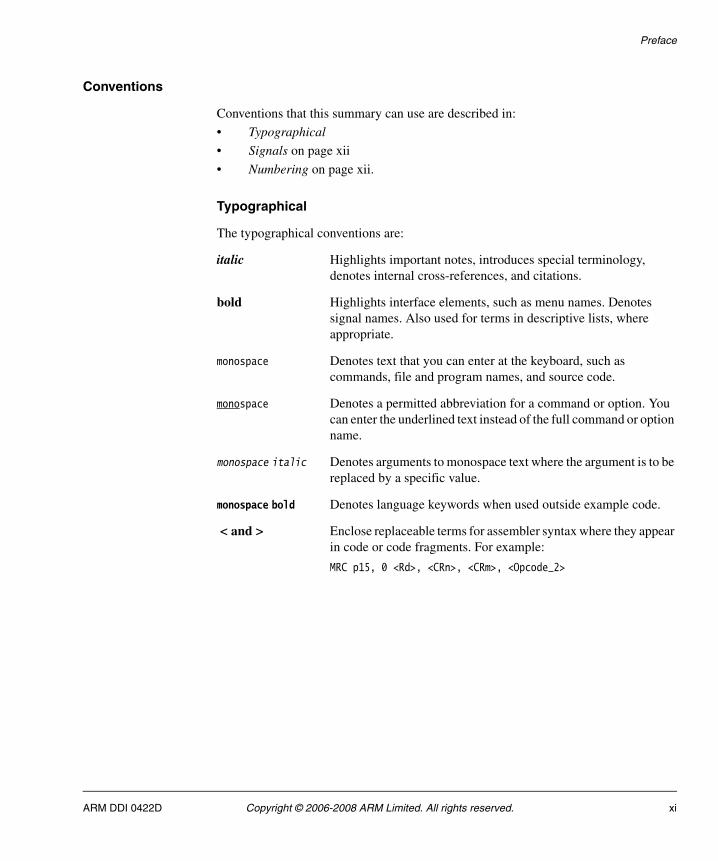
Conventions
Conventions that this summary can use are described in:
• Typographical
• Signals on page xii
• Numbering on page xii.
Typographical
The typographical conventions are:
italic Highlights important notes, introduces special terminology, denotes internal cross-references, and citations.
bold Highlights interface elements, such as menu names. Denotes signal names. Also used for terms in descriptive lists, where appropriate.
monospace Denotes text that you can enter at the keyboard, such as commands, file and program names, and source code.
monospace Denotes a permitted abbreviation for a command or option. You can enter the underlined text instead of the full command or option name.
monospace italic Denotes arguments to monospace text where the argument is to be replaced by a specific value.
monospace bold Denotes language keywords when used outside example code.
< and > Enclose replaceable terms for assembler syntax where they appear in code or code fragments. For example:
MRC p15, 0 <Rd>, <CRn>, <CRm>, <Opcode_2>
ARM DDI 0422D Copyright © 2006-2008 ARM Limited. All rights reserved. xi
Preface
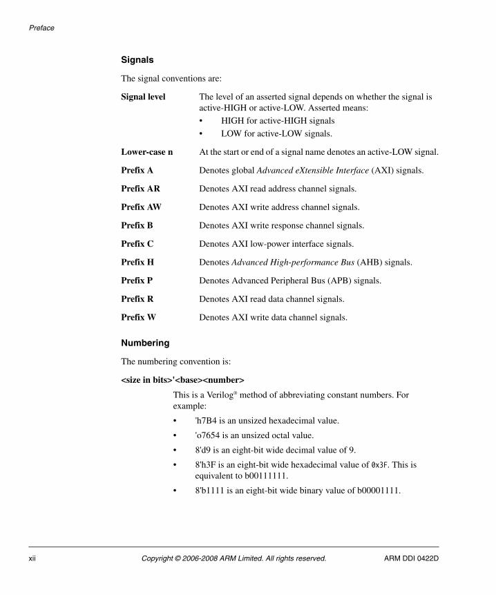
Signals
The signal conventions are:
Signal level The level of an asserted signal depends on whether the signal is active-HIGH or active-LOW. Asserted means:
• HIGH for active-HIGH signals
• LOW for active-LOW signals.
Lower-case n At the start or end of a signal name denotes an active-LOW signal.
Prefix A Denotes global Advanced eXtensible Interface (AXI) signals.
Prefix AR Denotes AXI read address channel signals.
Prefix AW Denotes AXI write address channel signals.
Prefix B Denotes AXI write response channel signals.
Prefix C Denotes AXI low-power interface signals.
Prefix H Denotes Advanced High-performance Bus (AHB) signals.
Prefix P Denotes Advanced Peripheral Bus (APB) signals.
Prefix R Denotes AXI read data channel signals.
Prefix W Denotes AXI write data channel signals.
Numbering
The numbering convention is:
<size in bits>'<base><number>
This is a Verilog® method of abbreviating constant numbers. For example:
• 'h7B4 is an unsized hexadecimal value.
• 'o7654 is an unsized octal value.
• 8'd9 is an eight-bit wide decimal value of 9.
• 8'h3F is an eight-bit wide hexadecimal value of 0x3F. This is equivalent to b00111111.
• 8'b1111 is an eight-bit wide binary value of b00001111.
xii Copyright © 2006-2008 ARM Limited. All rights reserved. ARM DDI 0422D

Preface
Additional reading
This section lists publications by ARM and by third parties.
See http://infocenter.arm.com/help/index.jsp for access to ARM documentation.
ARM publications
This summary contains information that is specific to the HPM. See the following documents for other relevant information:
• PrimeCell High-Performance Matrix (PL301) Technical Reference Manual (ARM DII 0397)
• PrimeCell High-Performance Matrix (PL301) Integration Manual (ARM DII 0157)
• AMBA Designer (FD001) User Guide (ARM DUI 0333)
• AMBA Designer (FD001) PrimeCell High-Performance Matrix (PL301) User Guide Supplement (ARM DUI 0333 Supplement 1)
• AMBA AXI Protocol v1.0 Specification (ARM IHI 0022)
• AMBA 3 AHB-Lite Protocol v1.0 Specification (ARM IHI 0033)
• AMBA 3 APB Protocol v1.0 Specification (ARM IHI 0024).
ARM DDI 0422D Copyright © 2006-2008 ARM Limited. All rights reserved. xiii
Preface
Feedback
ARM welcomes feedback on the HPM and its documentation.
Feedback on this product
If you have any comments or suggestions about this product, contact your supplier giving:
• the product name
• a concise explanation of your comments.
Feedback on this summary
If you have any comments on this summary, send an e-mail to [email protected]. Give:
• the title
• the number
• the relevant page number(s) to which your comments apply
• a concise explanation of your comments.
ARM also welcomes general suggestions for additions and improvements.
xiv Copyright © 2006-2008 ARM Limited. All rights reserved. ARM DDI 0422D

Chapter 1 Introduction
This chapter introduces the High-Performance Matrix (HPM). It contains the following sections:
• About the High-Performance Matrix on page 1-2
• Key features on page 1-4.
ARM DDI 0422D Copyright © 2006-2008 ARM Limited. All rights reserved. 1-1

Introduction
1.1 About the High-Performance Matrix
The HPM is a highly configurable auto-generated AMBA 3 bus subsystem, based around a high-performance AXI cross-bar switch known as the AXI bus matrix, and extended by AMBA infrastructure components. For information about these components, see the PrimeCell High-Performance Matrix (PL301) Technical Reference Manual.
This combination of IP provides support for other AMBA interface protocols including AHB-Lite and APB.
Use the AMBA Designer Graphical User Interface (GUI) based configuration tool to design your bus matrix. You can then generate, test, and profile complex AMBA bus systems in:
• a transaction-level modeling environment
• Verilog.
Figure 1-1 shows an example of the top-level hierarchy of an interconnect.
Figure 1-1 Example top-level hierarchy
1.1.1 Master and slave interfaces
The following terms apply in this summary:
• a master connects to a Slave Interface (SI)
• a slave connects to a Master Interface (MI).
See the Glossary for more information about masters, slaves, and their interfaces.
AXI bus matrix
AMBA AXI infrastructure components
AMBA AXI infrastructure components
AMBA Master Interface (MI) 0AMBA MI 1
AMBA MI n
AMBA Slave Interface (SI) 0
AMBA SI 1
AMBA SI n
HPM (PL301)
Global signals
... ...
APB programminginterface
1-2 Copyright © 2006-2008 ARM Limited. All rights reserved. ARM DDI 0422D

Introduction
When describing interconnect sizes, this summary first refers to the number of masters that you can connect to the interconnect, followed by the number of slaves. Therefore, a 3×4 interconnect interfaces to three AMBA masters and four AMBA slaves.
ARM DDI 0422D Copyright © 2006-2008 ARM Limited. All rights reserved. 1-3

Introduction
1.2 Key features
The HPM has:
• configurable number of SIs and MIs
• multi-layer AXI routing, suitable for high-performance applications
• sparse connection options to reduce gate count and improve security
• configurable AXI data widths
• configurable AHB-Lite data widths
• configurable address widths on AXI and AHB-Lite interfaces
• support for an AHB-Lite to AXI bridge optimized for use with memory controllers
• support for AMBA 2 APB and AMBA 3 APB at 32-bit data width
• decoded address register that you can configure for each SI
• flexible register stages to aid timing closure
• an arbitration mechanism that you can configure for each MI, implementing:
— a fixed Round-Robin (RR) scheme
— a programmable RR scheme
— a programmable scheme that provides prioritized groups of Least Recently Granted (LRG) arbitration.
• a programmable Quality of Service (QoS) scheme
• an APB interface to provide access to programming registers
• support for multiple clock domains:
— synchronous
— asynchronous.
• configurable cyclic dependency schemes to enable a master to have outstanding transactions to more than one slave
• PrimeCell ID register to aid self-discovery in systems
• a configurable memory map
• support for TrustZone® technology
1-4 Copyright © 2006-2008 ARM Limited. All rights reserved. ARM DDI 0422D
Introduction
• AXI and AHB USER signal support
• auto-generated Verilog
• auto-generated RTL testbench
• AMBA Designer tool-based configuration.
ARM DDI 0422D Copyright © 2006-2008 ARM Limited. All rights reserved. 1-5

Introduction
1-6 Copyright © 2006-2008 ARM Limited. All rights reserved. ARM DDI 0422D
Chapter 2 Programmable Features
This chapter describes the programmable features that you can manipulate. It contains the following sections:
• Programmable Quality of Service (ProgQoS) on page 2-2
• Arbitration scheme on page 2-4
• Summary of SI options on page 2-7
• Summary of MI options on page 2-8.
ARM DDI 0422D Copyright © 2006-2008 ARM Limited. All rights reserved. 2-1

Programmable Features
2.1 Programmable Quality of Service (ProgQoS)
The QoS scheme works by tracking the number of outstanding transactions, and when a specified number is reached, only permits transactions from particular, specified masters.
The QoS scheme only provides support for slaves that have a combined acceptance capability, such as the PrimeCell Dynamic Memory Controller (PL340).
The QoS scheme has no effect until the AXI bus matrix calculates that, at a particular MI, there are a number of outstanding transactions equal to the value stored in the QoS tidemark Register. It then accepts transactions only from slave ports specified in the QoS access control Register. This restriction remains until the number of outstanding transactions is again less than the value stored in the QoS tidemark Register. See QoS tidemark Register on page 3-4 and QoS access control Register on page 3-4.
It is recommended that you assign low MI numbers to MIs that require QoS support. This approach aligns well with the cyclic priority scheme because MIs that require QoS support are typically those that can be considered high-ranking slaves. See the PrimeCell High-Performance Matrix (PL301) Technical Reference Manual.
Figure 2-1 shows the implementation for an interconnect that supports two masters and one slave.
Figure 2-1 Example implementation of ProgQoS control registers for 2×1 interconnect
ID match valueQoS tidemark
ProgQoS control registersAPB
configuration port
Arbiter
MI 0 S0SI 0
SI 17-bit ID
M0
M1
2-bit ID
6-bit ID
AXI bus matrix
AMBA bus matrix
Arbiter scheme
QoS access control
2-2 Copyright © 2006-2008 ARM Limited. All rights reserved. ARM DDI 0422D

Programmable Features
Note When there is only one master, the QoS logic is removed as an optimization. However, the APB configuration interface enables you to program QoS parameters, but they have no effect.
For the programmers model, see Programmable Quality of Service (ProgQoS) on page 3-4.
ARM DDI 0422D Copyright © 2006-2008 ARM Limited. All rights reserved. 2-3
Programmable Features
2.2 Arbitration scheme
In the HPM, you can configure each MI separately to have an arbitration scheme that is either:
• a programmable or fixed Round-robin (RR) scheme
• a programmable Least Recently Granted (LRG) scheme.
The AW and AR channels have separate arbiters and can be programmed, if applicable, and interrogated separately through the APB programming interface, but both AW and AR channels are configured identically. Because the AW and AR channels are arbitrated separately, an MI can permit simultaneous read and write transactions from different SIs.
The arbitration mechanism registers the arbitration decision for use in the subsequent cycle. An arbitration decision taken in the current cycle does not affect the current cycle.
If no SIs are active, the arbiter adopts default arbitration, that is, the highest priority SI. If this occurs and then the highest priority interface becomes active in the same cycle as, or before any other SI, then this does not constitute a grant to an active SI and the arbitration scheme does not change its state as a result of that transfer.
If a QoS provision is enabled and active, only a subset of SIs are permitted to win arbitration, and it cannot be guaranteed that the default arbitration is among these. In these circumstances, no transaction is permitted to use the default arbitration, and arbitration must occur when there is an active SI.
The following sections describe the:
• RR schemes
• LRG scheme on page 2-5.
2.2.1 RR schemes
In these schemes, you can choose, at design time:
• the number of slots that are used
• the SI to which they are allocated
• their order.
There must be at least one slot per connected SI and there can be up to 32 slots. By allocating multiple slots for an SI, you can allocate access to the slave, on average, in proportion to the number of slots. If the slots are appropriately ordered, this can also reduce the maximum time before a grant is guaranteed. The SI associated with a slot can be interrogated from the APB programming interface and can be changed if the programmable RR scheme is chosen.
2-4 Copyright © 2006-2008 ARM Limited. All rights reserved. ARM DDI 0422D

Programmable Features
Whenever arbitration is granted to an active SI, the slots are rotated so that the slot currently in the highest priority position becomes the lowest, and all other slots move to a higher priority but maintain their relative order, as Figure 2-2 shows. This means that if an SI is the highest priority active SI, but is not the highest priority interface, then it continues to win the arbitration until it becomes the highest priority interface, and then the lowest priority interface subsequently.
Because the arbitration value is registered, the arbitration decision made in this cycle is used in the next cycle. This means that if the SI that currently holds the arbitration is still the highest priority active SI in this cycle, wins the arbitration again regardless of whether or not it is active in the next cycle as shown by the status of M3 in stages A, B, and C of Figure 2-2.
Figure 2-2 Example operation of RR arbitration scheme
2.2.2 LRG scheme
In this scheme, each connected SI has a single slot associated with it, but each interface also has a priority value. This priority value, whose post-reset value can be configured at design time and programmed or interrogated through the APB programming interface, can make the arbiter behave as:
• a pure LRG scheme
• a fixed priority encoder
• a combination of the two.
All masters with the same priority form a priority group. As a result of arbitration, a master can move within its priority group but cannot leave its group, and no new masters can join the group.
M0
M1
M2
M3
M0
M1
M2
M3
M3
M4
M5
M0
M4
M5
M0
M1
M4
M5
A B C D E
Indicates an inactive master
Indicates an active master
Stage
M4
M5 M1
M2
M2
M3
Indicates the master that won arbitration in the previous cycle
M0
M2
M3
M4
M5
M1
ARM DDI 0422D Copyright © 2006-2008 ARM Limited. All rights reserved. 2-5

Programmable Features
Arbitration is granted to the highest priority group from which a member is trying to win access, and within that group, to the highest master at that time. When a master wins arbitration, it is relegated to the bottom of its group to ensure that is cannot prevent other masters in its group from accessing the slave.
If you configure all master priorities to different levels, the arbiter implements a fixed priority scheme. This occurs because in this case, each master is in a group of its own, and therefore, masters maintain their ordering.
If all master priorities are the same, then an LRG scheme is implemented. The reason that it behaves as an LRG is because the process of relegating the master that was last granted access, to the bottom of its group, results in the masters being ordered from the LRG master at the top, to the most recently granted at the bottom.
The LRG and fixed priority modes concurrently exist when the master priority value registers are programmed with a combination of identical and unique values. You can mix priority groups that contain one member with priority groups that contain more than one member in an arbitrary manner. The arbiter places no restriction on the number of groups or their membership.
Figure 2-3 shows the movement of masters within their priority groups.
Figure 2-3 Example operation of LRG arbitration scheme
M0
M1
M2
M3
M0
M1
M3
M2
M0
M3
M2
M1
M0
M3
M2
M1
M0
M3
M2
M1
M4
M5
Group 1
A B C D E
Indicates a master
Indicates the master to which access is granted
Stage
M4
M5
M4
M5
M4
M5
M4
M5
Indicates movement of the arbitration winner
Indicates movement of other members of the arbitration winner’s group
Group 2
Group 3
2-6 Copyright © 2006-2008 ARM Limited. All rights reserved. ARM DDI 0422D

Programmable Features
2.3 Summary of SI options
Table 2-1 summarizes the standard SI options.
Table 2-1 SI configuration options summary
Option Description
Address tie-off The value of the address tie-off signals.a
Address width The number of address bits that the master provides.a
Clock domain crossing Provides an appropriate clock domain crossing bridge.a
Cyclic scheme The scheme that is implemented in the HPM to avoid cyclic dependency deadlock.a
Decode register Provides a single register stage in the address decoder, but at the expense of extra latency.a
ID width Number of bits for the ID bus of the SI. If this is zero, then these signals are
removed.a
Interface data width Number of bits for the data bus.a
Interface protocol When not set to AXI, instantiates an AHB-Lite to AXI component with the required AHB interface type.a
Name Name of the SI and associated top-level ports.a
Number Number of the SI.
Peripheral register slices Enables you to register the external inputs and outputs of the HPM appropriately for timing closure improvement by placing the required number of register slices between the boundary of the interconnect and the AXI bus matrix.a
Read acceptance capability Depth of the read control FIFOs on the SI.a
Sparse connect If you require sparse connectivity, this configuration option is assigned a list of the MIs
that the SI should connect to.a
Write acceptance capability Depth of the write control FIFOs on the SI.a
a. See the PrimeCell High-Performance Matrix (PL301) Technical Reference Manual.
ARM DDI 0422D Copyright © 2006-2008 ARM Limited. All rights reserved. 2-7

Programmable Features
2.4 Summary of MI options
Table 2-2 summarizes the standard MI options.
Table 2-2 MI configuration options summary
Option Description
Address tie-off The value of the address tie-off signals.a
Address width The number of address bits that the slave requires.a
Address range, high memory Upper bound of the address region of the MI.
Address range, low memory Lower bound of the address region of the MI.a
Address range, remap move Defines the behavior of the address remapping scheme for the MI, controlled by the REMAP bus.a
Clock domain crossing Provides an appropriate clock domain crossing bridge.a
Cyclic rank Number of the MI. This must be unique and it controls the cyclic priority and the layout of the QoS register interface.
Interface data width Number of bits for the data bus. This is limited to 32 bits for APB.a
Interface protocol When not set to AXI, instantiates either an AXI to AHB-Lite or AXI to APB bridge component as appropriate.a
Name Name of the MI and associated top-level ports.a
Peripheral register slices Enables you to register the external inputs and outputs of the HPM appropriately for timing closure improvement by placing the required number of register slices between the boundary of the interconnect and the AXI bus matrix.a
Programmable QoS Configures the HPM to use the programmable QoS scheme. See Programmable Quality of Service (ProgQoS) on page 2-2.
Remap range, bit Assigns the bit of the REMAP bus that is used for the remap alias. The least significant bit takes priority if more than one bit is active.a
Remap range, high memory Upper bound of the aliased address region of the MI when the relevant bit of the REMAP bus is HIGH.a
Remap range, low memory Lower bound of the aliased address region of the MI when the relevant bit of the REMAP bus is HIGH.a
Write interleave capability Number of active write transactions for which the MI is capable of transmitting data.a
Write issuing capability Maximum number of active write transactions that the MI can generate at any one time.a
2-8 Copyright © 2006-2008 ARM Limited. All rights reserved. ARM DDI 0422D

Programmable Features
Table 2-3 summarizes the MI options you require for each active APB peripheral slot if you configure an APB bridge.
a. See the PrimeCell High-Performance Matrix (PL301) Technical Reference Manual.
Table 2-3 MI configuration options summary for an APB bridge
Option Description
APB interface, slot ID Identifies the peripheral slot and indicates that it is to be connected to a peripheral.
APB interface, name The name of the slot, to be appended to the APB signal names at the HPM top-level.
APB interface, version Configures the APB protocol version for the slot. This can be 2.0 or 3.0.
ARM DDI 0422D Copyright © 2006-2008 ARM Limited. All rights reserved. 2-9

Programmable Features
2-10 Copyright © 2006-2008 ARM Limited. All rights reserved. ARM DDI 0422D

Chapter 3 Programmers Model
This chapter describes the registers that you can access by using the APB programming interface on the HPM. It contains the following sections:
• About the programmers model on page 3-2
• Register summary on page 3-3
• Programmable Quality of Service (ProgQoS) on page 3-4
• Arbitration control on page 3-6
• Configuration and ID registers on page 3-10.
ARM DDI 0422D Copyright © 2006-2008 ARM Limited. All rights reserved. 3-1

Programmers Model
3.1 About the programmers model
The following information applies to the HPM registers:
• The base address of the HPM is not fixed, and can be different for any particular system implementation. The offset of each register from the base address is fixed.
• Do not attempt to access reserved or unused address locations. Attempting to access these location can result in Unpredictable behavior of the HPM.
• Unless otherwise stated in the accompanying text:
— do not modify undefined register bits
— ignore undefined register bits on reads
— all register bits are reset to a logic 0 by a system or power-on reset.
• In Table 3-1 on page 3-3, the possible entries in the Type column are:
RW Read and write.
RO Read only.
WO Write only.
3-2 Copyright © 2006-2008 ARM Limited. All rights reserved. ARM DDI 0422D

Programmers Model
3.2 Register summary
Table 3-1 lists the HPM registers.
Table 3-1 HPM register summary
Offset Name Type Reset Width Description
0x400a QoS tidemark for MI 0 RW 0x00000000 32 See Programmable Quality of Service (ProgQoS) on page 3-40x404b QoS access control for MI 0 RW 0x00000000 32
0x408c AR channel arbitration value for MI 0 RW Configured 32 See Arbitration control on page 3-6
0x40Cd AW channel arbitration value for MI 0 RW Configured 32
0x800 - 0xFBC Reserved - - - -
0xFC0 PrimeCell Configuration Register 0 RO 0x000000nne 32 See Configuration registers on page 3-10
0xFC4 PrimeCell Configuration Register 1 RO 0x000000nne 32
0xFC8 PrimeCell Configuration Register 2 RO 0x00000000 32
0xFCC PrimeCell Configuration Register 3 RO 0x00000000 32
0xFD0 - 0xFDC Reserved - - - -
0xFE0 PrimeCell Peripheral Register 0 RO 0x01 8 See PrimeCell Peripheral ID Registers 0-3 on page 3-110xFE4 PrimeCell Peripheral Register 1 RO 0x13 8
0xFE8 PrimeCell Peripheral Register 2 RO 0x-4f 8
0xFEC PrimeCell Peripheral Register 3 RO 0x00 8
0xFF0 PrimeCell ID Register 0 RO 0x0D 8 See PrimeCell ID Registers 0-3 on page 3-14
0xFF4 PrimeCell ID Register 1 RO 0xF0 8
0xFF8 PrimeCell ID Register 2 RO 0x05 8
0xFFC PrimeCell ID Register 3 RO 0xB1 8
a. Address allocation for QoS tidemark Register is 0x400 + 0x20×N, where N is the number of the relevant MI.b. Address allocation for QoS access control Register is 0x404 + 0x20×N, where N is the number of the relevant MI.c. Address allocation for AR channel arbitration control registers is 0x408 + 0x20×N, where N is the number of the relevant MI.d. Address allocation for AW channel arbitration control registers is 0x40C + 0x20×N, where N is the number of the relevant MI.e. Where nn depends on the configuration of the HPM. See Configuration registers on page 3-10.f. Depends on the revision of the HPM. See Table 3-12 on page 3-13.
ARM DDI 0422D Copyright © 2006-2008 ARM Limited. All rights reserved. 3-3
Programmers Model
3.3 Programmable Quality of Service (ProgQoS)
This following sections describe:
• Address map
• QoS tidemark Register
• QoS access control Register.
See also Programmable Quality of Service (ProgQoS) on page 2-2.
3.3.1 Address map
The register space for the MIs starts at 0x400 and extends to 0x7FC. Each MI that is configured to support QoS filtering contains the registers at the following offsets:
• 0x0 – QoS tidemark Register
• 0x4 – QoS access control Register.
When more than one MI with QoS support is included then the MI number controls the register address offset for that MI, as Table 3-1 on page 3-3 lists.
3.3.2 QoS tidemark Register
You can program this with the number of outstanding transactions that are permitted before the QoS scheme becomes active.
If a value is written to this register that is larger than the combined acceptance capability of the attached slave, then the QoS scheme never becomes active for this MI. If a value of 0 is written to this register, then the QoS scheme is turned off for this MI. This behavior ensures that it is impossible to block all transactions completely by accidental mis-programming.
If you access a QoS tidemark Register for an MI that has not been configured to support QoS then the HPM ignores writes and reads are undefined.
3.3.3 QoS access control Register
A 1 in any bit of this register indicates that the SI corresponding to the bit position is permitted to use the reserved slots of the connected combined acceptance capability of the slaves.
The maximum value that you can write to this register is 2<total number of SIs> -1.
3-4 Copyright © 2006-2008 ARM Limited. All rights reserved. ARM DDI 0422D

Programmers Model
Note If you attempt to write a value containing 1s in positions that do not correspond to SIs, then these bits are ignored and are not set in the register.
Changes to these values occur on the first possible arbitration time after they are written.
If you access a QoS access control Register for an MI that has not been configured to support QoS then the HPM ignores writes and reads are undefined.
ARM DDI 0422D Copyright © 2006-2008 ARM Limited. All rights reserved. 3-5

Programmers Model
3.4 Arbitration control
The arbitration schemes for the AR channel and AW channel are set when you configure the HPM, and they control the arbitration scheme for these channels when the HPM exits from reset. However, the HPM enables you to change the AR channel and AW channel arbitration schemes by using the APB SI on the HPM to write to the arbitration control registers.
The HPM provides two arbitration control registers per MI, one for the AR channel and one for the AW channel. They operate and are programmed in the same way. See Table 3-1 on page 3-3 for their address locations.
As the address map does not have sufficient space for each value to be addressable separately, some addressing information is encoded in the write data when updating values. When reading registers the extra addressing information is supplied by a preliminary write command before the read command.
Note When a master interface has connections to only one slave interface its operation is much simpler and as a result the arbitration mechanism is removed. If you attempt to configure or interrogate the arbitration mechanism for such a master interface, all writes are ignored, and each read returns zero.
The following sections describe how to program the:
• Programmable Least Recently Granted (LRG) arbitration scheme
• Fixed Round-robin (RR) arbitration scheme on page 3-8
• Programmable RR arbitration scheme on page 3-8.
3.4.1 Programmable Least Recently Granted (LRG) arbitration scheme
The followings sections describe how to program and read the AR and AW channel arbitration values for the LRG arbitration scheme:
• Writing AR and AW channel arbitration values on page 3-7
• Reading AR and AW channel arbitration values on page 3-7.
3-6 Copyright © 2006-2008 ARM Limited. All rights reserved. ARM DDI 0422D

Programmers Model
Writing AR and AW channel arbitration values
Each slave interface that a master interface is connected to has one entry in the arbitration scheme. This entry is addressed by using the slave interface number. The slave interface number is encoded into bits [31:24] of the write data and the new priority value that is to be associated with that slave interface is encoded into bits [15:8] of the write data, as Table 3-2 lists.
Reading AR and AW channel arbitration values
You must perform a write followed by a read operation to the same address. The write transfer sets the interface number that you want to access. The following read operation returns the priority value for that interface number.
The write data is encoded with bits [31:24] set to 0xFF and the interface number whose value is to be returned encoded in bits [7:0], with all other bits set to 0.
Table 3-3 lists the bit assignments of the preliminary write operation.
The format of the read data has the priority value encoded in bits [15:8] and the slave interface number value echoed in bits [7:0]. All other bits are set to zero.
Table 3-2 Bit assignment for writing AR and AW channel arbitration values
Bits Name Description
[31:24] interface_number Slave interface number.
[23:16] - Set to zero.
[15:8] priority These bits set the interface priority value for the arbitration scheme. The range of values permitted is from 0 to 255 where:
• 0 is the highest priority
• 255 is the lowest priority.
[7:0] - Set to zero.
Table 3-3 Preliminary write bit assignment for an arbitration register read operation
Bits Name Description
[31:24] reserved Set to 0xFF
[23:8] reserved Set to 0x0000
[7:0] interface_number These bits set the interface number for the following read operation
ARM DDI 0422D Copyright © 2006-2008 ARM Limited. All rights reserved. 3-7

Programmers Model
Table 3-4 lists the bit assignments of the arbitration priority read operation.
3.4.2 Fixed Round-robin (RR) arbitration scheme
When the selected master interface is set to fixed RR arbitration scheme then writing to the configuration register has no effect and does not cause any APB bus errors. The HPM enables the configuration values to be read by using the method that Reading configuration values on page 3-9 describes.
3.4.3 Programmable RR arbitration scheme
The following sections describe how to program and read the values for the programmable RR arbitration scheme:
• Writing configuration values
• Reading configuration values on page 3-9.
Writing configuration values
When the programmable RR scheme is selected for a master interface then each of its arbitration slots can have the slave interface associated with it changed. See Table 3-5 for the bit assignments used to program a master interface slot number with its associated slave interface number.
Table 3-4 Bit assignment for an arbitration register read operation
Bits Name Description
[31:16] reserved These bits read as zero
[15:8] arb_priority Slave interface arbitration priority value
[7:0] interface_number Slave interface number
Table 3-5 Bit assignment for writing master interface channel arbitration values
Bits Name Description
[31:24] slot_number Arbitration slot number
[23:8] reserved Set to 0x0000
[7:0] slave_interface_num Slave interface number
3-8 Copyright © 2006-2008 ARM Limited. All rights reserved. ARM DDI 0422D
Programmers Model
Note No protection is imposed when you program the slots in the programmable RR arbitration scheme. So it is possible for you to remove a slave interface from all the slots which would make that slave interface inaccessible. However, if the mechanism for programming the configuration registers uses the interconnect, it is possible to make the configuration mechanism itself inaccessible.
Reading configuration values
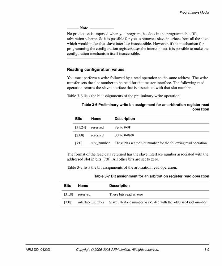
You must perform a write followed by a read operation to the same address. The write transfer sets the slot number to be read for that master interface. The following read operation returns the slave interface that is associated with that slot number.
Table 3-6 lists the bit assignments of the preliminary write operation.
The format of the read data returned has the slave interface number associated with the addressed slot in bits [7:0]. All other bits are set to zero.
Table 3-7 lists the bit assignments of the arbitration read operation.
Table 3-6 Preliminary write bit assignment for an arbitration register readoperation
Bits Name Description
[31:24] reserved Set to 0xFF
[23:8] reserved Set to 0x0000
[7:0] slot_number These bits set the slot number for the following read operation
Table 3-7 Bit assignment for an arbitration register read operation
Bits Name Description
[31:8] reserved These bits read as zero
[7:0] interface_number Slave interface number associated with the addressed slot number
ARM DDI 0422D Copyright © 2006-2008 ARM Limited. All rights reserved. 3-9

Programmers Model
3.5 Configuration and ID registers
The APB interface on the HPM must be capable of auto-discovery, and requires PrimeCell ID registers and configuration registers.
A standard structure is required, but it also assists intelligent programming of the programmable parts of the:
• arbitration policy
• QoS policy.
It does this by making data available on the number of MIs and SIs in the HPM.
Note The number of MIs does not include the MI to which the default slave is attached because this is not exposed.
3.5.1 Configuration registers
These are four 32-bit read-only registers at address 0xFC0-0xFCC. The register at:
• 0xFC0 is hard-coded and identifies how many SIs are configured in the HPM
• 0xFC4 is hard-coded and identifies how many MIs are configured in the HPM.
The registers at 0xFC8 and 0xFCC read as zeros.
Table 3-8 lists the register bit assignments.
Table 3-8 Configuration registers bit assignments
Bits Name Description
[31:8] - Undefined
[7:0] Config Identifies how many MIs or SIs are configured in the HPM:
0x0 = reserved
0x1 = one MI or SI
0x2 = two MIs or SIs
0x3 = 3 MIs or SIs
.
.
.
0x20 = 32 MIs or SIs
0x21-0xFF = reserved.
3-10 Copyright © 2006-2008 ARM Limited. All rights reserved. ARM DDI 0422D

Programmers Model
Figure 3-1 shows the register bit assignments.
Figure 3-1 Configuration registers bit assignments
3.5.2 PrimeCell Peripheral ID Registers 0-3
The periph_id registers are four eight-bit read-only registers, that can conceptually be treated as a single register that holds a 32-bit peripheral ID value. An external master reads them to determine the revision of the HPM. See Table 3-1 on page 3-3 for their address locations.
Table 3-9 lists the register bit assignments.
Figure 3-2 on page 3-12 shows the correspondence between bits of the periph_id registers and the conceptual 32-bit Peripheral ID Register.
31 8 7 0
ConfigUndefined
Table 3-9 periph_id Register bit assignments
Bits Name Description
[31:24] - Undefined.
[23:20] revision The peripheral revision number is revision-dependent.
[19:12] designer Designer’s ID number. This is 0x41 for ARM.
[11:0] part_number Identifies the peripheral. The part number for the HPM is 0x301.
ARM DDI 0422D Copyright © 2006-2008 ARM Limited. All rights reserved. 3-11

Programmers Model
Figure 3-2 periph_id Register bit assignments
The following sections describe the periph_id Registers:
• Peripheral Identification Register 0
• Peripheral Identification Register 1 on page 3-13
• Peripheral Identification Register 2 on page 3-13
• Peripheral Identification Register 3 on page 3-13.
Peripheral Identification Register 0
The periph_id_0 Register is hard-coded and the fields in the register control the reset value. Table 3-10 lists the register bit assignments.
7 0 7 4 3 0 7 4 3 0 7 0
31 24
Undefined
23 20
revision
19 16
designer_0
12
designer
15 11
part_number
8 7 0
Actual register bit assignment
Conceptual register bit assignment
Undefined revision designer_1 part_number_0part_number_1
Table 3-10 periph_id_0 Register bit assignments
Bits Name Description
[31:8] - Read undefined
[7:0] part_number_0 These bits read back as 0x01
3-12 Copyright © 2006-2008 ARM Limited. All rights reserved. ARM DDI 0422D

Programmers Model
Peripheral Identification Register 1
The periph_id_1 Register is hard-coded and the fields in the register control the reset value. Table 3-11 lists the register bit assignments.
Peripheral Identification Register 2
The periph_id_2 Register is hard-coded and the fields in the register control the reset value. Table 3-12 lists the register bit assignments.
Peripheral Identification Register 3
The periph_id_3 register is hard-coded and the fields in the register control the reset value. Table 3-13 lists the register bit assignments.
Table 3-11 periph_id_1 Register bit assignments
Bits Name Description
[31:8] - Read undefined
[7:4] designer_0 These bits read back as 0x1
[3:0] part_number_1 These bits read back as 0x3
Table 3-12 periph_id_2 Register bit assignments
Bits Name Description
[31:8] - Read undefined.
[7:4] revision These bits read back as the revision number. This can be between 0 and 15:
• 0x1 = r1p0
• 0x2 = r1p1
• 0x3 = r1p2.
[3:0] designer_1 These bits read back as 0x4.
Table 3-13 periph_id_3 Register bit assignments
Bits Name Description
[31:8] - Read undefined.
[7:4] - Reserved for future use. Read undefined.
[3:0] Reserved Always zero.
ARM DDI 0422D Copyright © 2006-2008 ARM Limited. All rights reserved. 3-13

Programmers Model
3.5.3 PrimeCell ID Registers 0-3
The PrimeCell ID value is a 32-bit value. However, to ensure that it is accessible in all systems, the 32 bits are implemented as four 8-bit registers. See Table 3-1 on page 3-3 for their address locations.
The registers can conceptually be treated as a single register that holds a 32-bit PrimeCell ID value. You can use the register for automatic BIOS configuration. The pcell_id Register is set to 0xB105F00D. You can access the register with one wait state. Table 3-14 lists the register bit assignments.
Figure 3-3 on page 3-15 shows the register bit assignments.
Table 3-14 pcell_id Register bit assignments
pcell_id_0-3 register
Bits Reset value Register Bits Description
- - pcell_id_3 [31:8] Read undefined
[31:24] 0xB1 pcell_id_3 [7:0] These bits read back as 0xB1
- - pcell_id_2 [31:8] Read undefined
[23:16] 0x05 pcell_id_2 [7:0] These bits read back as 0x05
- - pcell_id_1 [31:8] Read undefined
[15:8] 0xF0 pcell_id_1 [7:0] These bits read back as 0xF0
- - pcell_id_0 [31:8] Read undefined
[7:0] 0x0D pcell_id_0 [7:0] These bits read back as 0x0D
3-14 Copyright © 2006-2008 ARM Limited. All rights reserved. ARM DDI 0422D

Programmers Model
Figure 3-3 pcell_id Register bit assignments
The following sections describe the pcell_id Registers:
• PrimeCell Identification Register 0
• PrimeCell Identification Register 1 on page 3-16
• PrimeCell Identification Register 2 on page 3-16
• PrimeCell Identification Register 3 on page 3-16.
Note You cannot read these registers in the Reset state.
PrimeCell Identification Register 0
The pcell_id_0 Register is hard-coded and the fields in the register control the reset value. Table 3-15 lists the register bit assignments.
7 0 7 0 7 0 7 0
31 24
pcell_id_3
23 16 15 8 7 0
Actual register bit assignment
Conceptual register bit assignment
pcell_id_2 pcell_id_1 pcell_id_0
pcell_id_0pcell_id_1pcell_id_2pcell_id_3
Table 3-15 pcell_id_0 Register bit assignments
Bits Name Function
[31:8] - Reserved, read undefined
[7:0] pcell_id_0 These bits read back as 0x0D
ARM DDI 0422D Copyright © 2006-2008 ARM Limited. All rights reserved. 3-15

Programmers Model
PrimeCell Identification Register 1
The pcell_id_1 Register is hard-coded and the fields in the register control the reset value. Table 3-16 lists the register bit assignments.
PrimeCell Identification Register 2
The pcell_id_2 Register is hard-coded and the fields in the register control the reset value. Table 3-17 lists the register bit assignments.
PrimeCell Identification Register 3
The pcell_id_3 Register is hard-coded and the fields in the register control the reset value. Table 3-18 lists the register bit assignments.
Table 3-16 pcell_id_1 Register bit assignments
Bits Name Function
[31:8] - Reserved, read undefined
[7:0] pcell_id_1 These bits read back as 0xF0
Table 3-17 pcell_id_2 Register bit assignments
Bits Name Function
[31:8] - Reserved, read undefined
[7:0] pcell_id_2 These bits read back as 0x05
Table 3-18 pcell_id_3 Register bit assignments
Bits Name Function
[31:8] - Reserved, read undefined
[7:0] pcell_id_3 These bits read back as 0xB1
3-16 Copyright © 2006-2008 ARM Limited. All rights reserved. ARM DDI 0422D
Glossary
This glossary describes some of the terms used in technical documents from ARM.
Advanced eXtensible Interface (AXI)A bus protocol that supports separate address/control and data phases, unaligned data transfers using byte strobes, burst-based transactions with only start address issued, separate read and write data channels to enable low-cost DMA, ability to issue multiple outstanding addresses, out-of-order transaction completion, and easy addition of register stages to provide timing closure.
The AXI protocol also includes optional extensions to cover signaling for low-power operation.
AXI is targeted at high performance, high clock frequency system designs and includes a number of features that make it very suitable for high speed sub-micron interconnect.
Advanced High-performance Bus (AHB)A bus protocol with a fixed pipeline between address/control and data phases. It only supports a subset of the functionality provided by the AMBA AXI protocol. The full AMBA AHB protocol specification includes a number of features that are not commonly required for master and slave IP developments and ARM recommends only a subset of the protocol is usually used. This subset is defined as the AMBA AHB-Lite protocol.
See also Advanced Microcontroller Bus Architecture and AHB-Lite.
ARM DDI 0422D Copyright © 2006-2008 ARM Limited. All rights reserved. Glossary-1

Glossary
Advanced Microcontroller Bus Architecture (AMBA)A family of protocol specifications that describe a strategy for the interconnect. AMBA is the ARM open standard for on-chip buses. It is an on-chip bus specification that describes a strategy for the interconnection and management of functional blocks that make up a System-on-Chip (SoC). It aids in the development of embedded processors with one or more CPUs or signal processors and multiple peripherals. AMBA complements a reusable design methodology by defining a common backbone for SoC modules.
Advanced Peripheral Bus (APB)A simpler bus protocol than AXI and AHB. It is designed for use with ancillary or general-purpose peripherals such as timers, interrupt controllers, UARTs, and I/O ports. Connection to the main system bus is through a system-to-peripheral bus bridge that helps to reduce system power consumption.
AHB See Advanced High-performance Bus.
AHB-Lite A subset of the full AMBA AHB protocol specification. It provides all of the basic functions required by the majority of AMBA AHB slave and master designs, particularly when used with a multi-layer AMBA interconnect. In most cases, the extra facilities provided by a full AMBA AHB interface are implemented more efficiently by using an AMBA AXI protocol interface.
Aligned A data item stored at an address that is divisible by the number of bytes that defines the data size is said to be aligned. Aligned words and halfwords have addresses that are divisible by four and two respectively. The terms word-aligned and halfword-aligned therefore stipulate addresses that are divisible by four and two respectively.
AMBA See Advanced Microcontroller Bus Architecture.
APB See Advanced Peripheral Bus.
AXI See Advanced eXtensible Interface.
AXI channel order and interfacesThe block diagram shows:
• the order in which AXI channel signals are described
• the MI and SI conventions for AXI components.
AXI interconnect
Write address channel (AW)Write data channel (W)
Write response channel (B)Read address channel (AR)
Read data channel (R)
Write address channel (AW)Write data channel (W)
Write response channel (B)Read address channel (AR)
Read data channel (R)
AXI slave interface
AXI master interface
AXImaster
AXIslave
AXI master interface
AXI slave interface
Glossary-2 Copyright © 2006-2008 ARM Limited. All rights reserved. ARM DDI 0422D

Glossary
AXI terminology The following AXI terms are general. They apply to both masters and slaves:
Active read transaction
A transaction for which the read address has transferred, but the last read data has not yet transferred.
Active transfer
A transfer for which the xVALID1 handshake has asserted, but for which xREADY has not yet asserted.
Active write transaction
A transaction for which the write address or leading write data has transferred, but the write response has not yet transferred.
Completed transfer
A transfer for which the xVALID/xREADY handshake is complete.
Payload The non-handshake signals in a transfer.
Transaction An entire burst of transfers, comprising an address, one or more data transfers and a response transfer (writes only).
Transmit An initiator driving the payload and asserting the relevant xVALID signal.
Transfer A single exchange of information. That is, with one xVALID/xREADY handshake.
The following AXI terms are master interface attributes. To obtain optimum performance, they must be specified for all components with an AXI master interface:
Combined issuing capability
The maximum number of active transactions that a master interface can generate. It is specified for master interfaces that use combined storage for active write and read transactions. If not specified then it is assumed to be equal to the sum of the write and read issuing capabilities.
1. The letter x in the signal name denotes an AXI channel as follows:
AW Write address channel.
W Write data channel.
B Write response channel.
AR Read address channel.
R Read data channel.
ARM DDI 0422D Copyright © 2006-2008 ARM Limited. All rights reserved. Glossary-3

Glossary
Read ID capability
The maximum number of different ARID values that a master interface can generate for all active read transactions at any one time.
Read ID width
The number of bits in the ARID bus.
Read issuing capability
The maximum number of active read transactions that a master interface can generate.
Write ID capability
The maximum number of different AWID values that a master interface can generate for all active write transactions at any one time.
Write ID width
The number of bits in the AWID and WID buses.
Write interleave capability
The number of active write transactions for which the master interface is capable of transmitting data. This is counted from the earliest transaction.
Write issuing capability
The maximum number of active write transactions that a master interface can generate.
The following AXI terms are slave interface attributes. To obtain optimum performance, they must be specified for all components with an AXI slave interface:
Combined acceptance capability
The maximum number of active transactions that a slave interface can accept. It is specified for slave interfaces that use combined storage for active write and read transactions. If not specified then it is assumed to be equal to the sum of the write and read acceptance capabilities.
Read acceptance capability
The maximum number of active read transactions that a slave interface can accept.
Read data reordering depth
The number of active read transactions for which a slave interface can transmit data. This is counted from the earliest transaction.
Glossary-4 Copyright © 2006-2008 ARM Limited. All rights reserved. ARM DDI 0422D
Glossary
Write acceptance capability
The maximum number of active write transactions that a slave interface can accept.
Write interleave depth
The number of active write transactions for which the slave interface can receive data. This is counted from the earliest transaction.
Halfword A 16-bit data item.
Multi-layer An interconnect scheme similar to a cross-bar switch. Each master on the interconnect has a direct link to each slave, The link is not shared with other masters. This enables each master to process transfers in parallel with other masters. Contention only occurs in a multi-layer interconnect at a payload destination, typically the slave.
Processor A processor is the circuitry in a computer system required to process data using the computer instructions. It is an abbreviation of microprocessor. A clock source, power supplies, and main memory are also required to create a minimum complete working computer system.
Reserved A field in a control register or instruction format is reserved if the field is to be defined by the implementation, or produces Unpredictable results if the contents of the field are not zero. These fields are reserved for use in future extensions of the architecture or are implementation-specific. All reserved bits not used by the implementation must be written as 0 and read as 0.
Unaligned A data item stored at an address that is not divisible by the number of bytes that defines the data size is said to be unaligned. For example, a word stored at an address that is not divisible by four.
Unpredictable For reads, the data returned when reading from this location is unpredictable. It can have any value. For writes, writing to this location causes unpredictable behavior, or an unpredictable change in device configuration. Unpredictable instructions must not halt or hang the processor, or any part of the system.
Word A 32-bit data item.
ARM DDI 0422D Copyright © 2006-2008 ARM Limited. All rights reserved. Glossary-5

Glossary
Glossary-6 Copyright © 2006-2008 ARM Limited. All rights reserved. ARM DDI 0422D