Practical design and evaluation of an 800 W PFC boost converter ...
36
Application Note Please read the Important Notice and Warnings at the end of this document Revision 1.0 www.infineon.com/600v-c7 2015-11-26 AN_201409_PL52_012 Authors: Siu Ken, Franz Stückler Practical design and evaluation of an 800 W PFC boost converter using TO-247 4pin MOSFET 600 V CoolMOS™ C7 About this document Scope and purpose This document introduces use of the 600 V CoolMOS™ C7 TO-247-4 MOSFET in an 800 W power factor correction (PFC) boost converter design incorporating continuous conduction mode (CCM). The advantages and benefits of the TO-247-4 package are shown in terms of converter efficiency, gate to source voltage ringing and thermal behaviour. This document also covers support for PCB layout and driver selection that helps to improve EMI performance. This reference design is implemented on a 4-layer PCB and includes schematic and layout details. Intended audience This document is intended for design engineers who want to improve the performance of their applications and are considering implementing a TO-247 4pin package MOSFET in their powertrain. Table of Contents About this document ............................................................................................................................................. 1 1 Introduction ....................................................................................................................................... 3 1.1 Overview of server power supply design ................................................................................................ 3 1.2 Introduction of 4pin device – TO-247-4 .................................................................................................. 4 2 Device selection in the optimized CCM boost converter design ......................................................... 5 2.1 Selection of bulk capacitor ..................................................................................................................... 5 2.2 Selection of PFC inductor........................................................................................................................ 5 2.3 Choose of SiC (Silicon Carbide) diode .................................................................................................... 7 2.4 MOSFET requirement .............................................................................................................................. 7 3 Design Consideration with the use of TO-247 4pin MOSFET............................................................... 9 3.1 MOSFETs loss ........................................................................................................................................... 9 3.2 Circuit stability ...................................................................................................................................... 11 3.3 Driver design .......................................................................................................................................... 13 3.4 Schematic for the driver circuit ............................................................................................................ 13 3.5 Key features of the driving scheme ...................................................................................................... 13 3.6 EMI variation .......................................................................................................................................... 14 3.7 EMI information of the switching signal ............................................................................................... 15 3.8 Standard of the conductive EMI............................................................................................................ 16 3.9 Line EMI filter design ............................................................................................................................. 17 3.10 Layout consideration ............................................................................................................................ 18 3.11 Creepage and clearance........................................................................................................................ 18 3.11.1 Commutation loop ........................................................................................................................... 20 3.11.2 Gate to Drain coupling ..................................................................................................................... 20 3.11.3 Design overview ............................................................................................................................... 21 4 Application test ................................................................................................................................ 24
Transcript of Practical design and evaluation of an 800 W PFC boost converter ...

Application Note Please read the Important Notice and Warnings at the end of this document Revision 1.0
www.infineon.com/600v-c7 2015-11-26
AN_201409_PL52_012
Authors: Siu Ken, Franz Stückler
Practical design and evaluation of an 800 W PFC
boost converter using TO-247 4pin MOSFET
600 V CoolMOS™ C7
About this document
Scope and purpose
This document introduces use of the 600 V CoolMOS™ C7 TO-247-4 MOSFET in an 800 W power factor correction
(PFC) boost converter design incorporating continuous conduction mode (CCM). The advantages and benefits of the TO-247-4 package are shown in terms of converter efficiency, gate to source voltage ringing and thermal
behaviour. This document also covers support for PCB layout and driver selection that helps to improve EMI performance. This reference design is implemented on a 4-layer PCB and includes schematic and layout details.
Intended audience
This document is intended for design engineers who want to improve the performance of their applications and
are considering implementing a TO-247 4pin package MOSFET in their powertrain.
Table of Contents
About this document ............................................................................................................................................. 1
1 Introduction ....................................................................................................................................... 3 1.1 Overview of server power supply design ................................................................................................ 3
1.2 Introduction of 4pin device – TO-247-4 .................................................................................................. 4
2 Device selection in the optimized CCM boost converter design ......................................................... 5
2.1 Selection of bulk capacitor ..................................................................................................................... 5
2.2 Selection of PFC inductor........................................................................................................................ 5 2.3 Choose of SiC (Silicon Carbide) diode .................................................................................................... 7 2.4 MOSFET requirement .............................................................................................................................. 7
3 Design Consideration with the use of TO-247 4pin MOSFET............................................................... 9 3.1 MOSFETs loss ........................................................................................................................................... 9
3.2 Circuit stability ...................................................................................................................................... 11 3.3 Driver design .......................................................................................................................................... 13
3.4 Schematic for the driver circuit ............................................................................................................ 13
3.5 Key features of the driving scheme ...................................................................................................... 13 3.6 EMI variation .......................................................................................................................................... 14 3.7 EMI information of the switching signal ............................................................................................... 15 3.8 Standard of the conductive EMI............................................................................................................ 16
3.9 Line EMI filter design ............................................................................................................................. 17 3.10 Layout consideration ............................................................................................................................ 18 3.11 Creepage and clearance ........................................................................................................................ 18 3.11.1 Commutation loop ........................................................................................................................... 20 3.11.2 Gate to Drain coupling ..................................................................................................................... 20
3.11.3 Design overview ............................................................................................................................... 21
4 Application test ................................................................................................................................ 24

Application Note 2 Revision 1.0
2015-11-26
Practical design and evaluation of an 800 W PFC boost converter using
TO-247 4pin MOSFET 600 V CoolMOS™ C7 Introduction
4.1 Measurement technique ....................................................................................................................... 24 4.2 Operation test........................................................................................................................................ 25
4.3 Efficiency test ........................................................................................................................................ 27 4.4 Thermal measurement ......................................................................................................................... 28
4.5 Conducted EMI test ............................................................................................................................... 29
5 Summary .......................................................................................................................................... 33
6 Reference ......................................................................................................................................... 34
Revision History ................................................................................................................................................... 35

Application Note 3 Revision 1.0
2015-11-26
Practical design and evaluation of an 800 W PFC boost converter using
TO-247 4pin MOSFET 600 V CoolMOS™ C7 Introduction
1 Introduction
Efficient power conversion with high power density has become a necessary requirement of power circuitry
design. Nowadays, many organizations purchase information technology equipment based on the “80 PLUS® Titanium” efficiency specification, which requires peak efficiency at 96 % under half-load conditions. As a result the product design margin reduces significantly.
To satisfy the power designer’s needs in terms of efficiency and power density, Infineon launched the fastest switching performance CoolMOS™ C7 series to improve both switching losses and conduction loss [1]. However, this fast switching performance may introduce gate-to-source voltage ringing and electromagnetic
interference (EMI) issues due to geometrical limitations of the PCB layout between the MOSFET and driver. To overcome these challenges when using fast switching performance MOSFETs, a new package (TO-247-4) has been developed by Infineon.
Comparing this new package with the conventional TO-247, an additional source pin (“Kelvin connection”) is provided. This individual source pin could be independently connected to the gate driver control signal. The driver and power currents are separated to give stable control of the gate-to-source voltage signal [2]. By using
the TO-247-4 package, MOSFET switching speed will be further increased to improve efficiency of the converter with minimal design changes [3].
This application note is organized as follows. The device selection requirements will be given in section 1 (this section). In section 2, the design considerations of the TO-247-4 MOSFET are demonstrated to address any user concerns when changing devices. In section 3, the device test performance is shared as supporting information.
1.1 Overview of server power supply design
Reducing power consumption costs, minimizing maintenance costs, and increasing data center reliability are
general design targets of a server power supply. Among them, efficiency of the power unit is one of the key factors as electricity charges can account for more than 50% of the overall data center operation expenses.
Therefore, server power supply efficiency is critical to save the enterprise thousands of dollars annually on electric expenses.
The common form factor of a 1U server power supply (Figure 1) is used as our reference platform in the
following discussion. Normally the server power supply comprises several stages including the input line filter, a PFC stage, and a DC-DC stage for converting the AC input voltage to the regulated DC output voltage to support the daily operation of the server center.
Figure 1 An overview of a common server power supply
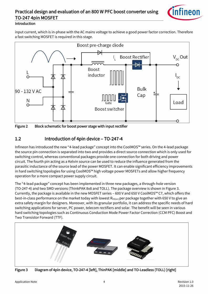
In this Application Note, the discussion will be focusing on the PFC stage, as shown in Figure 2, using the new TO-247 4pin package with the latest CoolMOS™ C7 MOSFET. The PFC stage always wants to draw a sinusoidal
Application Note 4 Revision 1.0
2015-11-26
Practical design and evaluation of an 800 W PFC boost converter using
TO-247 4pin MOSFET 600 V CoolMOS™ C7 Introduction
input current, which is in-phase with the AC mains voltage to achieve a good power factor correction. Therefore a fast switching MOSFET is required in this stage.
Figure 2 Block schematic for boost power stage with input rectifier
1.2 Introduction of 4pin device – TO-247-4
Infineon has introduced the new “4-lead package” concept into the CoolMOS™ series. On the 4-lead package
the source pin connection is separated into two and provides a direct source connection which is only used for
switching control, whereas conventional packages provide one connection for both driving and power circuit. The fourth pin acting as a Kelvin source can be used to reduce the influence generated from the
parasitic inductance of the source lead of the power MOSFET. It can enable significant efficiency improvements in hard switching topologies for using CoolMOS™ high voltage power MOSFETs and allow higher frequency operation for a more compact power supply circuit.
The “4-lead package” concept has been implemented in three new packages, a through-hole version (TO-247-4) and two SMD versions (ThinkPAK 8x8 and TOLL). The package overview is shown in Figure 3. Currently, the package is available in the new MOSFET series – 600 V and 650 V CoolMOS™ C7, which offers the
best-in-class performance on the market today with lowest RDS(on) per package together with 650 V to give an extra safety margin for designers. Moreover, with its granular portfolio, it can address the specific needs of hard
switching applications for server, PC power, telecom rectifiers and solar. The benefit will be seen in various hard switching topologies such as Continuous Conduction Mode Power Factor Correction (CCM PFC) Boost and Two Transistor Forward (TTF).
Figure 3 Diagram of 4pin device, TO-247-4 [left], ThinPAK [middle] and TO-Leadless (TOLL) [right]

Application Note 5 Revision 1.0
2015-11-26
Practical design and evaluation of an 800 W PFC boost converter using
TO-247 4pin MOSFET 600 V CoolMOS™ C7 Device selection in the optimized CCM boost converter design
2 Device selection in the optimized CCM boost converter design
The following are the converter design and power losses estimation equations for the CCM operated boost converter. The design example specifications listed in Table 1 will be used for all of the equation calculations. Also the boost converter encounters the maximum current stress and power losses at the minimum line voltage
condition (Vac.min); hence, all design equations and power losses will be calculated using the low line voltage condition as the worst case consideration.
Table 1 Specifications on the designed power stage
Input voltage 85-265 VAC @ 50 Hz
Output voltage 400 V
Maximum power steady state 800 W
Switching frequency 130 kHz
Inductor current ripple 25% @ low line/full load
Output voltage 120 Hz ripple 20 Vp-p
Hold-up time 10 ms @ VO_min=340 V
2.1 Selection of bulk capacitor
The output capacitor is sized to meet both of the hold-up time (10 ms) and the low frequency voltage ripple (20 V) requirements. The capacitor value is selected to have the larger value between the two equations below:
𝐶𝑜 ≥2 ∙ 𝑃𝑜 ∙ 𝑡ℎ𝑜𝑙𝑑
𝑉𝑜2 − 𝑉𝑜.𝑚𝑖𝑛
2 =2 ∙ 800𝑊 ∙ 16.6 ∙ 10−3𝑠𝑒𝑐
(400𝑉)2 − (340𝑉)2= 360.4 𝜇𝐹 (1)
𝐶𝑜 ≥𝑃𝑜
2 ∙ 𝜋 ∙ 𝑓𝑙𝑖𝑛𝑒 ∙ ∆𝑉𝑜 ∙ 𝑉𝑜=
800𝑊
2 ∙ 𝜋 ∙ 50𝐻𝑧 ∙ 20𝑉 ∙ 400𝑉= 318.3 𝜇𝐹 (2)
→ 𝐶𝑜 = 𝑚𝑎𝑥 (360.4 𝜇𝐹 ,318.3 𝜇𝐹) = 360.4 𝜇𝐹
In this design we use one 390 µF capacitor with a 450 V voltage class.
2.2 Selection of PFC inductor
The filter inductor value is determined based on the specified maximum inductor current ripple and the corresponding operation conditions as shown below:
𝐿 =1
%𝑅𝑖𝑝𝑝𝑙𝑒 ∙
1
𝜂 ∙
𝑉𝑎𝑐.𝑚𝑖𝑛 2
𝑃𝑜
(1 −√2 ∙ 𝑉𝑎𝑐 .𝑚𝑖𝑛
𝑉𝑜
) ∙1
𝑓𝑠𝑤 =
1
0.25 ∙
(85𝑉)2
800𝑊(1 −
√2 ∙ 85𝑉
400𝑉) ∙
1
130 ∙ 103𝐻𝑧 = 202.2 𝜇𝐻 (3)
In the inductor selection process, the first consideration is to address the loss optimization. Balancing between
core loss and copper loss, a suitable inductor size can be selected and the corresponding winding requirement can be calculated. The second consideration is the impedance characteristic of the inductor across the overall frequency range. This characteristic will influence the differential mode noise behaviour of the PFC circuit.
Especially in the high frequency part, the higher the impedance level of the inductor, the lower differential mode noise that will be observed in the line. To fulfil this requirement, a smaller parasitic capacitance of the inductor (capacitor coupling from copper wire) is required. Larger core size or higher core permeability can also effectively reduce the parasitic capacitance of the inductor due to less winding. However, core loss will
increase as a result. Therefore we need to maintain a balance between the inductor performance and the core efficiency.

Application Note 6 Revision 1.0
2015-11-26
Practical design and evaluation of an 800 W PFC boost converter using
TO-247 4pin MOSFET 600 V CoolMOS™ C7 Device selection in the optimized CCM boost converter design
High efficiency and high power density is a design requirement of switch mode power supply (SMPS) design. To achieve this requirement, fast switching devices are required to coordinate with the system operation
frequency increases. By increasing the switching frequency, the inductance value of the inductor can be reduced, deriving several benefits. Firstly, the system power density is increased as a smaller core size can be selected.
Another benefit of the inductance reduction is to minimize the induced Cusp distortion, which is one of the input current distortions that appear in the zero crossings of the input voltage. In the zero crossings state, the current waveform always fails to follow the pre-set sinewave envelope. This is because the inductor current cannot increase until the voltage is above zero. [4] The instantaneous time period can be expressed as:
t =2
ω∙ tan−1(g ∙ ω ∙ L) (4)
From the expression, we know that if the inductor value is larger or the required power level is higher, the Cusp
distortion will become more significant. Therefore the smaller the inductance value, the better the Cusp distortion and the power factor can be achieved.
In our design a 130 kHz, 75 µ permeability Kool Mu core from Magnetics Inc. is used. It consists of 2 stacked Kool
Mu 77553 toroid’s with 55 turns of AWG 14 copper wire as shown in Figure 4b. Compared with the inductor used for 65 kHz switching frequency, the toroid has a 49 % volume reduction. At the same time, inductor in the low line full load scenario can achieve 33 % reduction in overall loss.
a) Inductor for 65 kHz b) Inductor for 130 kHz
Figure 4 PFC inductor for different switching frequencies
With the use of a network analyser, the impedance magnitude of the inductor can be measured and the curve is shown in Figure 5 over the frequency range of 100 kHz to 30 MHz. In the measured frequency period, two
resonant valleys are observed in impedance performance of the 65 kHz inductor. However in the curve for the 130 kHz inductor, one of the resonant valleys is pushed higher than 30MHz, which means there will be less high EMI noise peaks appearing in this showed frequency range. Also the overview of the impedance performance of the 130 kHz inductor is better than the 65 kHz inductor in the MHz frequency range, this will benefit the EMI filter design especially in the conductive EMI phase.

Application Note 7 Revision 1.0
2015-11-26
Practical design and evaluation of an 800 W PFC boost converter using
TO-247 4pin MOSFET 600 V CoolMOS™ C7 Device selection in the optimized CCM boost converter design
Figure 5 The inductor impedance against different testing frequencies
2.3 Choose of SiC (Silicon Carbide) diode
Selection of the boost diode is a major design decision in a CCM boost converter since the diode is hard
commutated at a high current, and the reverse recovery can cause significant power loss, noise and current
spikes. Reverse recovery can be a bottleneck for high switching frequency and high power density power
supplies. For Infineon’s leading edge technologies, the 650 V thinQ!™ SiC Schottky Diode Generation 5 is highly
recommended to be applied in the CCM boost application. This new family of products can provide an efficiency improvement in all load conditions with the result that the improved thermal performance has an
improved figure of merit (Qc x Vf).
To determine the current rating of a SiC diode, there is a rule of thumb for a CCM-PFC-system - the SiC diode can handle an output power (POUT) of 100 W per rated ampere of the diode. In this design example, for an 800 W we require a 8 A diode, therefore SiC diode IDH8G65C5 is selected.
2.4 MOSFET requirement
The selection of the optimum on state resistance of a specific CoolMOS™ series is based on a balance between
switching losses and conduction losses of the device at a targeted load point. [5] This can be done by modelling
all losses in a software tool such as Mathcad and evaluating different technologies and device on-state resistance.
Several CoolMOS™ series MOSFETs can be used for boost applications. CoolMOS™C7 followed by CP provides the fastest switching and with the TO-247 4pin package the influence of the package inductance can be further
minimized. Hence, the best performance can be achieved in high power density and high efficiency platform design. When switching frequency increases, the benefit of the TO-247 4pin in the CoolMOS™C7 series becomes more beneficial. At the same time, a higher Rdson device can be selected after the loss optimization, which can reduce the design cost.
In our design example, an IPZ60R099C7 is used as the PFC MOSFET as a result of the optimization.

Application Note 8 Revision 1.0
2015-11-26
Practical design and evaluation of an 800 W PFC boost converter using
TO-247 4pin MOSFET 600 V CoolMOS™ C7 Device selection in the optimized CCM boost converter design
At the same time, the MOSFET junction temperature needs to be maintained below the safety temperature during system operation. By using the loss calculation equation, the overall power consumption can be
estimated. Combining this with the system operation details (air flow condition, environmental temperature, etc.), a suitable heatsink can be selected to provide a sufficient cooling environment for the MOSFET.
In the common through-hole package configuration, the heatsink is attached to the backside of the device and
an insulator is inserted between the package and heatsink to isolate the drain connection for safety reasons. However, a parasitic capacitance will be generated between the device drain pad and the heat sink. This will be one of the sources to induce common mode noise. The higher the parasitic value, the higher the common mode noise will be observed in the high frequency part of the EMI. Therefore a good insulator with a low parasitic capacitance characteristic is always required in the design.

Application Note 9 Revision 1.0
2015-11-26
Practical design and evaluation of an 800 W PFC boost converter using
TO-247 4pin MOSFET 600 V CoolMOS™ C7 Design Consideration with the use of TO-247 4pin MOSFET
3 Design Consideration with the use of TO-247 4pin MOSFET
3.1 MOSFETs loss
In the switching losses prediction, the average input current is used to estimate the losses over the line cycle.
The calculation is based on the switching time consideration, where the triangular area between current and voltage changing corresponds to the switching losses. The simplified MOSFET waveform during the turn-on and turn-off process is shown in Figure 6.
Vds
Id
t6 t7 t8 t9 t
Vgs(th)
QG(SW)
QG(TOT)
Vgs
QG(TH)
Vgs(miller)
Vds
Id
t1 t2 t3 t4 t
Vgs(th)
QG(SW)
QG(TOT)
Vgs
QG(TH)
Vgs(miller)
. . . . . .
t5
Figure 6 Simplified turn on and turn off waveform
In the standard operation, the channel of the MOSFET will build up or break down as the MOSFET switches on
and off at the transient periods t2 and t8 of Figure 6. This will cause a fast drain current change at this state.
Ld
Ls
Rg
Cds
Cgd
Cgs
Ld
Ls
Rg
Cds
Cgd
Cgs
PWMin
VoutVcc
Rb
Id
Igd
Igs
Ig
Vout
IgdIg
Igs Id
PWMin
Vcc
Rb
Figure 7 Driving circuit of TO-247 4pin package (left) and TO-247 standard package (right)
In a common gate driver arrangement, as shown in left side of the Figure 7, the fast current transient causes a voltage drop VLS across the source parasitic inductance of the MOSFET which can counteract the driving voltage. The induced source voltage, VLS = L*di/dt, can reduce the gate current therefore slowing down the switching transient and increasing the associated energy loss. Therefore the switching time is increased and this causes the switching loss to be higher.

Application Note 10 Revision 1.0
2015-11-26
Practical design and evaluation of an 800 W PFC boost converter using
TO-247 4pin MOSFET 600 V CoolMOS™ C7 Design Consideration with the use of TO-247 4pin MOSFET
In order to explain the positive effect of the additional source pin for the gate drive even better, one can see in the comparison of Figure 8 and Figure 9 how the source induced voltage caused by the drain current feedbacks into the gate loop at 3pin devices, but do not have any impact on the 4pin devices.
Figure 8 Simulated turn-on for standard 3pin device
Figure 9 Simulated turn-on for 4pin device
The calculation of turn-on time and losses for 3pin devices are:
𝑡𝑜𝑛 = (𝑅𝑔 ∙ 𝐶𝑖𝑠𝑠 + 𝐿𝑆 ∙ 𝑔𝑓𝑠) ∙ 𝑙𝑛 (𝑉𝑔𝑜𝑛
− 𝑉𝑔𝑠(𝑡ℎ)
𝑉𝑔𝑜𝑛− 𝑉𝑔𝑠(𝑀𝑖𝑙𝑙𝑒𝑟)
) + 𝐶𝑟𝑠𝑠 ∙ 𝑅𝑔 ∙ (𝑉𝑑𝑠 − 𝑉𝑔𝑠(𝑀𝑖𝑙𝑙𝑒𝑟)
𝑉𝑔𝑜𝑛− 𝑉𝑔𝑠(𝑀𝑖𝑙𝑙𝑒𝑟)
) (5)

Application Note 11 Revision 1.0
2015-11-26
Practical design and evaluation of an 800 W PFC boost converter using
TO-247 4pin MOSFET 600 V CoolMOS™ C7 Design Consideration with the use of TO-247 4pin MOSFET
𝑃𝑆.𝑜𝑛 = 0.5 ∙ 𝐼𝐿.𝑎𝑣𝑔 ∙ 𝑉𝑜 ∙ 𝑡𝑜𝑛 ∙ 𝑓 (6)
Turn-off time and loss are:
𝑡𝑜𝑓𝑓 = 𝐶𝑟𝑠𝑠 ∙ 𝑅𝑔 ∙ (𝑉𝑑𝑠 − 𝑉𝑔𝑠(𝑀𝑖𝑙𝑙𝑒𝑟)
𝑉𝑔𝑠(𝑀𝑖𝑙𝑙𝑒𝑟)) + (𝑅𝑔 ∙ 𝐶𝑖𝑠𝑠 + 𝐿𝑆 ∙ 𝑔𝑓𝑠) ∙ 𝑙𝑛 (
𝑉𝑔𝑠(𝑀𝑖𝑙𝑙𝑒𝑟) − 𝑉𝑔_𝑜𝑓𝑓
𝑉𝑔𝑠(𝑡ℎ) − 𝑉𝑔_𝑜𝑓𝑓) (7)
𝑃𝑆.𝑜𝑓𝑓 = 0.5 ∙ 𝐼𝐿.𝑎𝑣𝑔 ∙ 𝑉𝑜 ∙ 𝑡𝑜𝑓𝑓 ∙ 𝑓 (8)
In the 4pin MOSFET optimized circuit, as shown in figure 7b, the kelvin-source package concept is to exclude
the package source inductance and layout inductance from the driving loop, so that the L*di/dot induced
voltage is outside the gate drive loop and not affecting the gate current and switching losses. The switching time estimation equation is renewed as follows:
Turn-on time calculation for 4pin device:
𝑡𝑜𝑛 = 𝑅𝑔 ∙ 𝐶𝑖𝑠𝑠 ∙ 𝑙𝑛 (𝑉𝑔_𝑜𝑛 − 𝑉𝑔𝑠(𝑡ℎ)
𝑉𝑔_𝑜𝑛 − 𝑉𝑔𝑠(𝑀𝑖𝑙𝑙𝑒𝑟)) + 𝐶𝑟𝑠𝑠 ∙ 𝑅𝑔 ∙ (
𝑉𝑑𝑠 − 𝑉𝑔𝑠(𝑀𝑖𝑙𝑙𝑒𝑟)
𝑉𝑔_𝑜𝑛 − 𝑉𝑔𝑠(𝑀𝑖𝑙𝑙𝑒𝑟)) (9)
Turn-off time is:
𝑡𝑜𝑓𝑓 = 𝐶𝑟𝑠𝑠 ∙ 𝑅𝑔 ∙ (𝑉𝑑𝑠 − 𝑉𝑔𝑠(𝑀𝑖𝑙𝑙𝑒𝑟)
𝑉𝑔𝑠(𝑀𝑖𝑙𝑙𝑒𝑟)) + 𝑅𝑔 ∙ 𝐶𝑖𝑠𝑠 ∙ 𝑙𝑛 (
𝑉𝑔𝑠(𝑀𝑖𝑙𝑙𝑒𝑟) − 𝑉𝑔𝑜𝑓𝑓
𝑉𝑔𝑠(𝑡ℎ) − 𝑉𝑔𝑜𝑓𝑓
) (10)
The above is the “classic” format for calculating turn-off time and loss, but due to the high Cuss at lo drain
voltages of Super Junction MOSFETs, the actual turn-off losses with fast switching can be up to 50% lower than calculated. The current flow through the drain during turn-off under these conditions is non-dissipative
capacitive current, and with fast drive, the channel may be completely turned off by the onset of drain voltage rise.
The phenomenon is named as early channel shun down or capacitive turn-off. It is related to the gate voltage level in miller plateau which appears in the turn-off transient state t7 as shown in the Figure 6. In this state, The
MOSFET output capacitor Coss will be charged up by the whole load current to re-build the space charge region. The gate voltage will not show any significant gate plateau as this effective Miller plateau voltage of the turn-off case is defined as:
𝑉𝑚 =
𝑉𝑡ℎ +𝐼𝐷
𝑔𝑓𝑠
𝐶𝑜𝑠𝑠𝑔𝑓𝑠 ∙ 𝑅𝑔 ∙ 𝐶𝑔𝑑
+ 1 (11)
This level depends on several device and circuit parameter, such as gate resistor, device output capacitance
and gate to drain capacitance. If the level is below the threshold voltage, the channel will be shut down earlier than in the classic turn-off, which happens under following condition:
𝑉𝑡ℎ ∙𝐶𝑜𝑠𝑠
𝐶𝑔𝑑> 𝑅𝑔 ∙ 𝐼𝐷 (12)
Therefore the current flow in this case will follow the capacitance characteristic due to the fact that the device
channel is already completely turned off before the drain source voltage start to rise.
3.2 Circuit stability
Apart from influencing the MOSFET switching speed in the fast transient period, the package parasitic inductance will also influence the quality of the gate driving signal by the introduced oscillation loops.
Application Note 12 Revision 1.0
2015-11-26
Practical design and evaluation of an 800 W PFC boost converter using
TO-247 4pin MOSFET 600 V CoolMOS™ C7 Design Consideration with the use of TO-247 4pin MOSFET
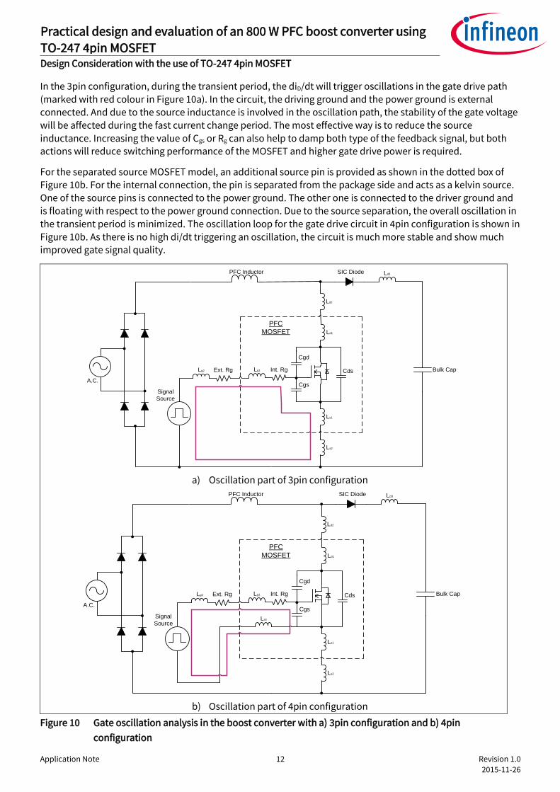
In the 3pin configuration, during the transient period, the diD/dt will trigger oscillations in the gate drive path (marked with red colour in Figure 10a). In the circuit, the driving ground and the power ground is external
connected. And due to the source inductance is involved in the oscillation path, the stability of the gate voltage will be affected during the fast current change period. The most effective way is to reduce the source
inductance. Increasing the value of Cgs or Rg can also help to damp both type of the feedback signal, but both actions will reduce switching performance of the MOSFET and higher gate drive power is required.
For the separated source MOSFET model, an additional source pin is provided as shown in the dotted box of Figure 10b. For the internal connection, the pin is separated from the package side and acts as a kelvin source. One of the source pins is connected to the power ground. The other one is connected to the driver ground and is floating with respect to the power ground connection. Due to the source separation, the overall oscillation in
the transient period is minimized. The oscillation loop for the gate drive circuit in 4pin configuration is shown in Figure 10b. As there is no high di/dt triggering an oscillation, the circuit is much more stable and show much improved gate signal quality.
Ld1
Ls1
PFC
MOSFET
Int. Rg
SIC Diode
Bulk Cap
PFC Inductor
Cds
Signal
Source
A.C.
Ld3
Cgd
Cgs
Lg1
Ls2
Ld2
Ext. RgLg2
a) Oscillation part of 3pin configuration
Ld1
Ls1
PFC
MOSFET
Int. Rg
SIC Diode
Bulk Cap
PFC Inductor
Cds
Signal
Source
A.C.
Ld3
Cgd
Cgs
Lg1
Ls2
Ld2
Ext. RgLg2
Lss
b) Oscillation part of 4pin configuration
Figure 10 Gate oscillation analysis in the boost converter with a) 3pin configuration and b) 4pin
configuration

Application Note 13 Revision 1.0
2015-11-26
Practical design and evaluation of an 800 W PFC boost converter using
TO-247 4pin MOSFET 600 V CoolMOS™ C7 Design Consideration with the use of TO-247 4pin MOSFET
3.3 Driver design
In our reference design, a boost converter circuit is used to demonstrate the driving circuit design with the use of the TO-247-4 pin device.
3.4 Schematic for the driver circuit
To maximize the benefit of the TO-247 4pin device, the driver ground should connect to the kelvin source pin,
(source sense - “SS”) in order to separate the driving current path from the main power line current. The
configurations of the driver circuits are shown in Figure 11.
With the source separation, the impact of the source inductors on the gate driving circuit in the transient period will be eliminated. The voltage drop induced by the source inductor (VLs) will no longer influence the gate to
source voltage, Vgs(t). This results in the switching transient period being shorter and reduces the switching
losses in the device compared with the operation waveform of the TO-247 package MOSFET. With the use of the
driver ground, the new TO-247-4 MOSFET allows relatively fast switching operation resulting in reduced switching losses and the MOSFET performance can be further enhanced.
Figure 11 Recommended driving circuit for the TO-247 standard package (left) and TO-247 4pin package
(right)
3.5 Key features of the driving scheme
There are two different approaches for the driving schematic. One is connected with a non-isolated driver and the other one is connected by an isolated driver.
The detailed schematic of the driving circuit of the TO-247-4 with a non-isolated driver is given in Figure 12. In this schematic there are two filters added into the driving loop. When the 4pin device is used for the design, a
bias filter and PWM input filter is required to filter the driver ground shift, generated by the MOSFET power source inductance.
In the design of the signal filter, the cut off frequency should be ten times higher than the PWM signal frequency due to the low pass RC filter characteristic. The VCC bias filter is another low pass RC filter that is added to the IC
VCC supply. The bias resistor is used to control maximum displacement current during operation. The bypass capacitor also functions to limit the ripple voltage in the VCC supply when charging and discharging the
MOSFETs gate. The ground in the driver loop is not allowed to connect back to the power ground otherwise this would short the source inductance and causing high peak current in the kelvin source pin.

Application Note 14 Revision 1.0
2015-11-26
Practical design and evaluation of an 800 W PFC boost converter using
TO-247 4pin MOSFET 600 V CoolMOS™ C7 Design Consideration with the use of TO-247 4pin MOSFET
Figure 12 Detailed schematic of the TO-247 4pin driving circuit with the use of a non-isolated driver
For the TO-247 4pin MOSFET driven with the isolated driver, the corresponding circuit schematic is shown in Figure 13. As the isolated driver IC is used, the input filter is no longer required as the signal source is
completely isolated from the MOSFET gate driver circuit. The only element that remains in the circuit is the Vcc protection in case the VCC is referred to power ground. In this case the resistor is used to control maximum
displacement current during operation. The capacitor value selection is based on the VCC ripple requirement and to maintain the VCC level during the charge and discharge process. If VCC for the driver is offered by
additional floating flyback winding, than the bias resistor is not required any more. In this case the isolated
ground of the floating VCC for the driver has to be connected to the kelvin source pin. For both of this variant with the isolated driver, the maximum switching frequency is not limited like with the non-isolated version.
Figure 13 Detail schematic of the TO-247 4pin driving circuit with the use of an isolated driver
3.6 EMI variation
EMI is a very important quality factor for a switch mode power supply (SMPS) - especially related to the power
switches in the SMPS which are the main source of EMI based on the fast switching (high di/dt and dv/dt).

Application Note 15 Revision 1.0
2015-11-26
Practical design and evaluation of an 800 W PFC boost converter using
TO-247 4pin MOSFET 600 V CoolMOS™ C7 Design Consideration with the use of TO-247 4pin MOSFET
Normally, the PFC circuit will be the first input stage that connects to the mains for the equipment. Therefore the design and its operational behaviour are also highly related to the EMI behaviour of the overall circuit and directly influence the input EMI filter design.
In the PFC stage, the differential mode noise is induced by the MOSFET switching current and the circuit parameters. The common mode noise is caused by a current induced by the high dv/dt in the switching with
the parasitic capacitors coupled to ground. A suitable filter design is needed based on the noise spectrum and the EMI standard requirement.
3.7 EMI information of the switching signal
To understand more about the noise spectrum of the EMI, we can convert the power switching signal from the
time domain to frequency domain by a Fourier transformation. The real switching waveform of the MOSFET during the turn-on and the turn-off transient period will be a trapezoidal signal.
The trapezoidal signal of function f(t) can be represented by an infinite Fourier series as:
𝑓(𝑡) = ∑ 𝐶𝑛𝑒𝑗𝑛𝜔0𝑡
∞
𝑛=−∞
(13)
And 𝐶𝑛 can be expressed as:
𝐶𝑛 =1
𝑇∫ 𝐴(𝑡)
𝑡0+𝑇
𝑡0
∙ 𝑒−𝑗𝑛𝜔0𝑡 𝑑𝑡 = 𝐴0 ∙𝑡𝑖
𝑇∙ sinc(𝑛𝜔0
𝑡𝑖
2) ∙ sinc(𝑛𝜔0
𝑡𝑠
2) ∙ 𝑒−𝑗𝑛𝜔0
𝑡𝑖+𝑡𝑠2
Therefore, for the trapezoidal waveform examined above, the logarithmic value of its envelope is given by:
20𝑙𝑜𝑔10(𝑒𝑛𝑣𝑒𝑙𝑜𝑝𝑒) = 20𝑙𝑜𝑔10 (2 ∙ 𝐴0 ∙𝑡𝑖
𝑇) + 20𝑙𝑜𝑔10 |sinc(
𝜋𝑡𝑖
𝑇)| + 20𝑙𝑜𝑔10 |sinc (
𝜋𝑡𝑠
𝑇)| (14)
In the frequency domain of the trapezoidal signal, the first cutoff frequency can be determined by the signal
pulse width and the spectrum components will decrease by -20 dB per decade after the first cut off. The second cut off frequency depends on the rise time/fall time. The spectrum will have a dropping slope of -40 dB per decade starting at the second cutoff frequency. The spectrum is shown in Figure 14.
From the equation and the frequency spectrum, a summary that relates to the MOSFET operation can be
derived.
− The spectrum amplitude is related to the loading condition
− The higher the device switching frequency (with the same signal amplitude and duty), the more the first cutoff point will shift to a higher frequency
− Operating the device under faster switching conditions will mean that the second cutoff point will also shift to a higher frequency

Application Note 16 Revision 1.0
2015-11-26
Practical design and evaluation of an 800 W PFC boost converter using
TO-247 4pin MOSFET 600 V CoolMOS™ C7 Design Consideration with the use of TO-247 4pin MOSFET
Figure 14 The trapezoidal switching signal and the corresponding frequency domain
3.8 Standard of the conductive EMI
In European design, Information Technology equipment needs to comply with the Emissions Standards CISPR
22/EN55022 “Information Technology equipment – Radio disturbance characteristics – Limits and methods of measurement”. In the EMI standard requirement, all server power designs are Class B devices with a specified emission limit line.
The EMI requirement is split into radiated and conducted aspects. For the described evaluation PFC board it is
more important to investigate the conducted EMI behaviour since it is the input stage of any SMPS below a
certain power range. The measurement range of the conducted EMI is from 150 kHz to 30 MHz. The details of the measurement setup are described in the CISPR 16-2-1 “Methods of measurement of disturbances and immunity – Conducted disturbance measurements”. Two limit lines are required - One is a quasi-peak standard line and the other is an average line. The requirements for the dB level are shown in Figure 15.
Figure 15 Standard of the conducted EMI based on EN55022

Application Note 17 Revision 1.0
2015-11-26
Practical design and evaluation of an 800 W PFC boost converter using
TO-247 4pin MOSFET 600 V CoolMOS™ C7 Design Consideration with the use of TO-247 4pin MOSFET
3.9 Line EMI filter design
From the signal Fourier series expression, we know that the influence resulting from the package replacement
will not have a large effect in frequency domain. Therefore, the EMI filter design of TO-247 4pin can remain the
same as for the TO-247 package.
In the filter selection, there are numerous EMI filters that could be considered for noise reduction, but the most
commonly used are the LC filter and the Pi filter. In our circuit a Pi filter is added in the input stage, as shown in Figure 16. This is a low impedance feedthrough filter with two capacitors with one inductive element between. Ideally, it should be used where both source and load are high impedance systems so that it can provide the maximum mismatch on its port. This characteristic is mismatched to the server system, as the LISN circuit and
the boost converter of the PFC stage, the input and output stage of the filter, are all also considered as high
impedance networks. Therefore the low impedance characteristics of the Pi filter can provide the best filter function to the system.
While a triple element filter (Pi) theoretically yields 60 dB per decade, in practise the insertion loss curves do not exactly match the predictions. The impedances of the chosen electrical configuration in the source and load may also be influenced by the level of attenuation of the filter at various frequencies.
High
Impedance
(50Ω)
High
ImpedanceLo
w
Imp
ed
an
ce
Source/LISN Input Filter Boost Converter
Hig
h
Imp
ed
an
ce
Lo
w
Imp
ed
an
ce
Figure 16 Block diagram of the input stage with Pi filter
The overview of the EMI filter design, as shown in Figure 16, can separated into two filter parts: one for common
mode noise and one for differential mode noise. The circuit of the common mode filter and the different mode
filter functions to suppress different types of noise. The common mode filter includes a common choke in the ac power line and the X capacitor around the line to suppress the common mode noise generated from the
system. The differential mode filter normally uses the leakage part of the common mode choke to be the
differential mode inductor together with the Y capacitor connecting to ground to suppress the differential mode noise.
The reference design of the EMI filter is shown in Figure 17a, the choke L1 is the common mode inductor, X2-capacitor is the C4/C5 and Y2-capacitors are C17/C18. The corresponding equivalent circuit of the common mode circuit and differential mode circuit is also shown in the same figure.

Application Note 18 Revision 1.0
2015-11-26
Practical design and evaluation of an 800 W PFC boost converter using
TO-247 4pin MOSFET 600 V CoolMOS™ C7 Design Consideration with the use of TO-247 4pin MOSFET
LCM
LDM
CX1
1.5uF
LISN
CY
3.3nF
CY
3.3nF
Switching
Power Supply
L
G
N
50Ω
50Ω
EMI Filter
LCM
CX2
1.5uF
Boost Converter
LDM
2.4mH
9.6uH
(leakage of
LCM)
LCMLDM/2
LISN
Switching
Power Supply25Ω
EMI Filter Boost Converter
2.4uH 2.4mH 2 x CY
6.6nF
2 x LDM
CX1
1.5uF
LISN
Switching
Power Supply100Ω
EMI Filter
CX2
1.5uF
Boost Converter
9.6mH CY/2
1.65nF
a) Overview of the EMI filter in the input state
b) Common Mode Circuit
c) Differential Mode Circuit
Figure 17 The reference EMI filter for the demo PFC circuit together with the circuit analysis
3.10 Layout consideration
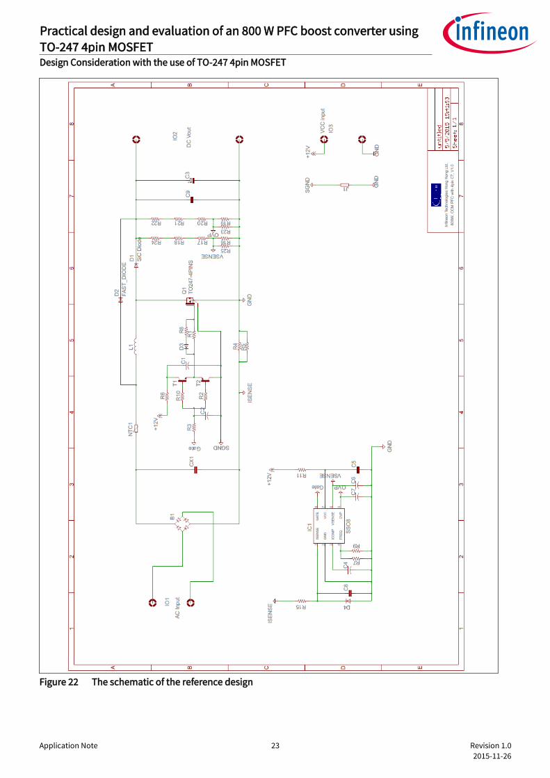
For the reference design, a 52 mm x 125 mm 4-layer PCB layout is used. The detail of the board layout is shown in Figure 21which is related to the schematic in Figure 22. The layer structure of the board is shown below:
− Layer 1: Components
− Layer 2: Power
− Layer 3: GND
− Layer 4: Signal
3.11 Creepage and clearance
For product safety, the dimensions of the creepage and clearance distances are very critical in the high voltage
circuit and are specified to avoid the risks of fire, electric shock or current leakage that may happen during operation. PCB designs need to fulfil a conformance standard requirement.
In Europe, battery-powered Information Technology equipment needs to follow the design requirements of EN60950. The standard covers AC adapters, server power supplies, telecom rectifiers, USB chargers etc. The
C5 C4
L1 C17
C18

Application Note 19 Revision 1.0
2015-11-26
Practical design and evaluation of an 800 W PFC boost converter using
TO-247 4pin MOSFET 600 V CoolMOS™ C7 Design Consideration with the use of TO-247 4pin MOSFET
important design requirements include the minimum allowable PCB spacing that can be determined from EN 60950-1 2nd Edition Tables 2K, 2L, 2M or 2N.
These tables specify so-called "creepage" and "clearance" distances for various grades of insulation as functions of the working voltage, pollution degree, PCB material group and coating. The definition of clearance is the shortest distance between two conductive parts, or between a conductive part and the bounding surface
of the equipment, measured through air. Creepage distance is defined as the shortest path between two conductive parts, or between a conductive part and the bounding surface of the equipment, measured along the surface of the insulation.
Below is an example for the requirements of a high voltage MOSFET in a PFC circuit.
1. System condition on minimum clearance distance
− Insulation : Functional
− Pollution Degree : 2
− Nominal AC Main : ≤300 V
− r.m.s working voltage : 285 V
− Peak working voltage : 650 V
2. System condition on minimum creepage distance
− Insulation : Functional
− Pollution Degree : 2
− Material Group : IIIa or IIIb
− r.m.s working voltage : 285 V
3. System condition on minimum separation distances for coated printed boards
− Insulation : Functional
− d.c working voltage : 285 V
4. Results for the trace between drain and source
− The minimum clearance : 2 mm
− The minimum creepage : 3 mm
− The minimum separation distances for coated printed boards : 1 mm
The new package layout can also fulfil these minimum distance requirements and is able to be directly used to
replace the TO-247 package device without any extra changes in the pin layout. A reference model is shown as below:
Figure 18 TO-247 4pin package reference model in board layout

Application Note 20 Revision 1.0
2015-11-26
Practical design and evaluation of an 800 W PFC boost converter using
TO-247 4pin MOSFET 600 V CoolMOS™ C7 Design Consideration with the use of TO-247 4pin MOSFET
3.11.1 Commutation loop
With this new package layout, the commutation loop between the MOSFET and the diode can be further
minimized when compared with the TO-247 package. In the traditional arrangement with the standard
package, the Gate pin of the MOSFET stays between the MOSFET Drain and the Anode of the diode in the commutation path. It results in a long routing being required and at the same time more noise is generated.
However due to the rearrangement of pins in the new device, the drain pin of the TO-247 4pin package is located at the left corner area. It allows the anode of the PFC diode to be placed right behind the drain pin of the PFC MOSFET without any other connection between them. The recommended pin arrangement for the TO-247-4 MOSFET in a PFC circuit is shown in Figure 19. This arrangement can benefit the system by having less
noise coupling to the switching circuit and therefore a much clear waveform can be obtained during platform operation.
3.11.2 Gate to Drain coupling
In the new TO-247 4pin package the drain pin and the gate pin are separated by the source connection pin
allowing reduction of the critical drain to gate coupling, which often causes gate oscillations at turn off with high dv/dt rates of the Drain-Source voltage (VDS). In the standard arrangement, the gate is just behind the drain pin. Due to the circuit connection, there always appears a strong coupling effect between the drain and the gate, which is strongly not recommended. In the circuit layout design, the drain power line and gate control line should not be parallel or have any close interaction / coupling.
Figure 19 The commutation in the layout and the parasitic capacitor Cgd induced from the connection point
is highlighted

Application Note 21 Revision 1.0
2015-11-26
Practical design and evaluation of an 800 W PFC boost converter using
TO-247 4pin MOSFET 600 V CoolMOS™ C7 Design Consideration with the use of TO-247 4pin MOSFET
3.11.3 Design overview
The details of the reference design are included in the following figures (Figure 20 to Figure 22).
Figure 20 Overview of the reference layout

Application Note 22 Revision 1.0
2015-11-26
Practical design and evaluation of an 800 W PFC boost converter using
TO-247 4pin MOSFET 600 V CoolMOS™ C7 Design Consideration with the use of TO-247 4pin MOSFET
Figure 21 The 4 layers of the PCB layout for the reference design, including layer 1 (top side), layer
2(interlayer), layer 3(interlayer) and layer 4 (mirror of bottom side)
Application Note 23 Revision 1.0
2015-11-26
Practical design and evaluation of an 800 W PFC boost converter using
TO-247 4pin MOSFET 600 V CoolMOS™ C7 Design Consideration with the use of TO-247 4pin MOSFET
Figure 22 The schematic of the reference design

Application Note 24 Revision 1.0
2015-11-26
Practical design and evaluation of an 800 W PFC boost converter using
TO-247 4pin MOSFET 600 V CoolMOS™ C7 Application test
4 Application test
4.1 Measurement technique
For the precise waveform measurement, it is important to minimize the effect of the measurement process and
to correctly select the measurement point. For the current measurement, extra care is always required as an extra current loop will be generated from the measurement setup. The loop may easily couple the high frequency noise and parasitic inductance of the current measurement probe and may affect the accuracy of the
measured waveform. Therefore the measurement loop must be constrained to a small area and to minimize as much as possible the length to minimize the influence on the device performance and the system operation. For the voltage measurement, a voltage probe is commonly used for the precise waveform measurement in the target platform. For the probe connection, the measurement loop of the probe adaptor should be constrained to a small area to minimize the noise coupling. An example of the voltage measurement is shown in Figure 23.
Figure 23 Optimization of the voltage measurement with standard voltage probe setup (left) and voltage
adaptor (right)
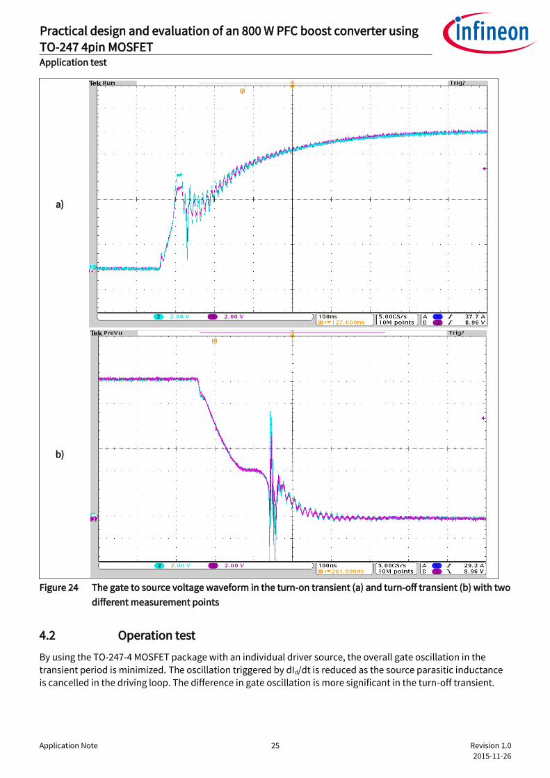
The probe connection point is also very critical to the performance analysis, especially during the transient
period. It should always be placed at the closest point to the target measurement pin to avoid any unwanted signal pick up influencing the measurement results, such as the oscillation signal in the circuit parasitic
components or any current/voltage set in parasitic components during the transient operation. For example, in Figure 24 there is a set of MOSFET transient gate to source voltage waveforms. The pink line is the
measurement of the gate voltage at the closest point to the MOSFET lead pin. The blue line is the measurement
performed 10 mm away from the closest point. It can be clearly observed that for the same waveform, under the same measurement setup, different results can be obtained due to the difference in measurement points.
In this case, if the measurement point of the MOSFET source is not closest to the soldering pin, a high level of oscillation in the gate voltage waveform will be measured and lead to a mis-measurement.
Application Note 25 Revision 1.0
2015-11-26
Practical design and evaluation of an 800 W PFC boost converter using
TO-247 4pin MOSFET 600 V CoolMOS™ C7 Application test
a)
b)
Figure 24 The gate to source voltage waveform in the turn-on transient (a) and turn-off transient (b) with two
different measurement points
4.2 Operation test
By using the TO-247-4 MOSFET package with an individual driver source, the overall gate oscillation in the
transient period is minimized. The oscillation triggered by dId/dt is reduced as the source parasitic inductance is cancelled in the driving loop. The difference in gate oscillation is more significant in the turn-off transient.

Application Note 26 Revision 1.0
2015-11-26
Practical design and evaluation of an 800 W PFC boost converter using
TO-247 4pin MOSFET 600 V CoolMOS™ C7 Application test
Also in the TO-247 4pin package, the voltage drop induced by the source inductor (VLs) will no longer influence the gate to source voltage, Vgs(t), therefore the switching speed is further enhanced. A faster transient time during turn-on and off can be observed in the operation and the design margin can be increased.
Figure 25 Turn-on transient waveform of IPW60R099C7 and IPZ60R099C7
-5
0
5
10
15
20
-1,00E-07 -5,00E-08 0,00E+00 5,00E-08 1,00E-07 1,50E-07
Vg
s /V
Time /s
Turn-on transient waveform
Vgs of 3pin connection
Vgs of 4pin connection
-6
0
6
12
18
24
30
36
-100
0
100
200
300
400
500
600
-1,00E-07 -5,00E-08 0,00E+00 5,00E-08 1,00E-07 1,50E-07
Vd
s /V
Time /s
Turn-on transient waveform
Vds of 3pin connection
Vds of 4pin connection
Id of 3pin connection
Id of 4pin connectionId
/A
Application Note 27 Revision 1.0
2015-11-26
Practical design and evaluation of an 800 W PFC boost converter using
TO-247 4pin MOSFET 600 V CoolMOS™ C7 Application test
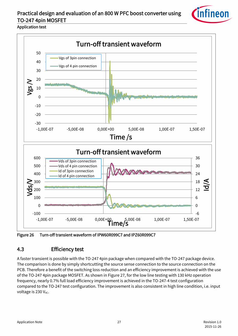
Figure 26 Turn-off transient waveform of IPW60R099C7 and IPZ60R099C7
4.3 Efficiency test
A faster transient is possible with the TO-247 4pin package when compared with the TO-247 package device.
The comparison is done by simply shortcutting the source sense connection to the source connection on the
PCB. Therefore a benefit of the switching loss reduction and an efficiency improvement is achieved with the use of the TO-247 4pin package MOSFET. As shown in Figure 27, for the low line testing with 130 kHz operation
frequency, nearly 0.7% full load efficiency improvement is achieved in the TO-247-4 test configuration compared to the TO-247 test configuration. The improvement is also consistent in high line condition, i.e. input voltage is 230 VAC.
-30
-20
-10
0
10
20
30
40
50
-1,00E-07 -5,00E-08 0,00E+00 5,00E-08 1,00E-07 1,50E-07
Vg
s /V
Time /s
Turn-off transient waveform
Vgs of 3pin connection
Vgs of 4 pin connection
-6
0
6
12
18
24
30
36
-100
0
100
200
300
400
500
600
-1,00E-07 -5,00E-08 0,00E+00 5,00E-08 1,00E-07 1,50E-07
Vd
s/V
Time/s
Turn-off transient waveform Vds of 3pin connectionVds of 4 pin connectionId of 3pin connectionId of 4 pin connection
Id/A

Application Note 28 Revision 1.0
2015-11-26
Practical design and evaluation of an 800 W PFC boost converter using
TO-247 4pin MOSFET 600 V CoolMOS™ C7 Application test
a)
b)
Figure 27 Efficiency comparison of TO-247 and TO-247-4 pin package in the PFC unit under low line (a) and
high line (b) operation
4.4 Thermal measurement
The thermal conductivity of the TO-247 and TO-247 4pin package MOSFETs are the same; there is no change in
the thermal resistance of the package as the source separation is done internally. Therefore the same thermal
characteristics table is provided in both the TO-247 and TO-247-4 MOSFET datasheets. Figure 28 shows an example from the IPZ60R099C7 and IPW60R099C7 datasheets.
95
95,5
96
96,5
97
97,5
98
98,5
0 200 400 600 800
Eff
icie
ncy
[%
]
Power [W]
Efficiency high line (230 VAC)
130 kHz 4pin
130 kHz 3pin
65 kHz 4pin
65 kHz 3pin
95
95,5
96
96,5
97
97,5
98
98,5
0 200 400 600 800
Eff
icie
ncy
[%
]
Power [W]
Efficiency high line (230 VAC)
130 kHz 4pin
130 kHz 3pin
65 kHz 4pin
65 kHz 3pin

Application Note 29 Revision 1.0
2015-11-26
Practical design and evaluation of an 800 W PFC boost converter using
TO-247 4pin MOSFET 600 V CoolMOS™ C7 Application test
Figure 28 Thermal characteristics for both IPZ60R099C7 and IPW60R099C7
𝑇𝑗 = (𝑅𝑡ℎ𝑗𝑐+ 𝑅𝑡ℎ𝑐𝑎) ∗ 𝑃𝑑𝑒𝑣𝑖𝑐𝑒 + 𝑇𝑎𝑚𝑏 (13)
The temperature difference in the device will be directly proportional to the power losses of the MOSFET, as
shown in eq. 13. Consistent with the efficiency data, a system using a TO-247 package MOSFET will have a result in higher MOSFET temperature compared to same system but with TO-247 4pin. A thermal record is shown in
Table 2 which corresponds to the test results in the above measurement. In the low line testing (85 VAC), the difference in the recorded case temperature is up to 15 degrees.
Table 2 Thermal performance of the MOSFET under different testing conditions at 130 kHz
Package 85 VAC 50% load 85 VAC 100% load 230 VAC 50% load 230 VAC 100% load
TO-247 59.4°C 94°C 52.2°C 54.6°C
TO-247-4 57°C 78.2°C 51.2°C 53.2°C
4.5 Conducted EMI test
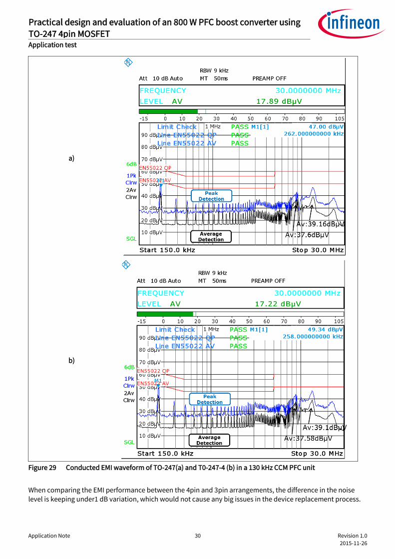
When replacing the TO-247 with a TO-247-4, the variation in the EMI remains in an acceptable range and it
mainly comes from the faster switching performance during transients. The low line measurement results are provided in Figure 29 and Figure 30. Both of the packages meet the EMI average and quasi-peak requirements in their section. Also they have enough design margin of 6 dB, before approaching the limitation line.
Application Note 30 Revision 1.0
2015-11-26
Practical design and evaluation of an 800 W PFC boost converter using
TO-247 4pin MOSFET 600 V CoolMOS™ C7 Application test
a)
b)
Figure 29 Conducted EMI waveform of TO-247(a) and T0-247-4 (b) in a 130 kHz CCM PFC unit
When comparing the EMI performance between the 4pin and 3pin arrangements, the difference in the noise level is keeping under1 dB variation, which would not cause any big issues in the device replacement process.
Application Note 31 Revision 1.0
2015-11-26
Practical design and evaluation of an 800 W PFC boost converter using
TO-247 4pin MOSFET 600 V CoolMOS™ C7 Application test
a)
b)
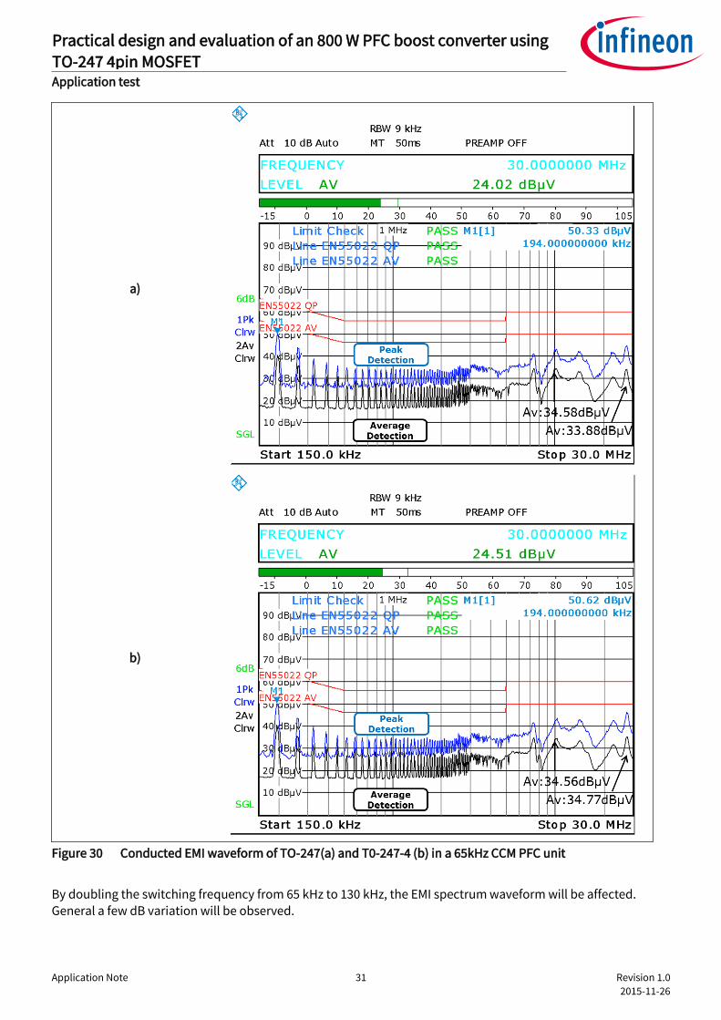
Figure 30 Conducted EMI waveform of TO-247(a) and T0-247-4 (b) in a 65kHz CCM PFC unit
By doubling the switching frequency from 65 kHz to 130 kHz, the EMI spectrum waveform will be affected. General a few dB variation will be observed.

Application Note 32 Revision 1.0
2015-11-26
Practical design and evaluation of an 800 W PFC boost converter using
TO-247 4pin MOSFET 600 V CoolMOS™ C7 Application test
In the low frequency range (150 kHz to 1MHz), the main different which can be observed from the spectrum is the level of the harmonic peak. In the 65 kHz switching frequency platform, the first EMI peak appearing in the
measurement is the third harmonic which is indicated at 195 kHz. When the platform operation frequency is doubled to 130 kHz, the second harmonic with frequency 260 kHz will be the first EMI peak appearing in the
measurement. In general, the second harmonic peak is higher than the third harmonic peak. However under the EMI filter condition, the 260 kHz noise peak will obtain a better filtering than the 195 kHz noise peak as the
closest the filter corner frequency the least EMI noise can be filtered. Therefore only a few dB differences in the first EMI noise peak can be observed with two different switching frequency platforms.
In the high frequency range (>1 MHz), due to the switching frequency is doubled in the 130 kHz platform, the overall noise level in the high frequency part is also higher causing by later cut off in spectrum. Due to the
inductor is changed, the sharped in the EMI graph is also different. In the 130 kHz design, the highest EMI noise peak has been appeared in the 13 MHz frequency which is matched with the resonant valley of the inductor.

Application Note 33 Revision 1.0
2015-11-26
Practical design and evaluation of an 800 W PFC boost converter using
TO-247 4pin MOSFET 600 V CoolMOS™ C7 Summary
5 Summary
In this application note, a reference design for an 800 W PFC converter is demonstrated with the CoolMOS™ C7 TO-247-4 MOSFET. In the evaluation, the improvement of the TO-247-4 MOSFET compared to the TO-247 MOSFET can be observed as higher platform efficiency and easier usage with less gate oscillation.
At the same time it has been shown, that the EMI performance of the TO-247-4 MOSFET is able to maintain a
similar noise level without any extra design effort. In the reference design, the driving scheme and the recommended pin arrangement is also demonstrated to provide a full picture of the TO-247-4 MOSFET in the design process of the PFC stage in the server power supply.

Application Note 34 Revision 1.0
2015-11-26
Practical design and evaluation of an 800 W PFC boost converter using
TO-247 4pin MOSFET 600 V CoolMOS™ C7 Reference
6 Reference
[1] F. Stueckler, E. Vecino, Infineon Technologies Application Note: “CoolMOSTM C7 650V Switch in a Kelvin Source Configuration”. May 2013.
[2] http://www.infineon.com/dgdl/Infineon+-+Application+Note+-+TO-247-4pin+-+650V+CoolMOS™
+C7+Switch+in+a+Kelvin+Source+Configuration.pdf?folderId=db3a304333b8a7ca0133c6bec0956188&fileId=db3a30433e5a5024013e6a9908a26410
[3] J. Hancock, F. Stueckler, E. Vecino, Infineon Technologies Application Note: “CoolMOS™ C7 : Mastering the Art of Quickness”. April 2013.
[4] http://www.infineon.com/dgdl/Infineon+-+Application+Note+-+650V+CoolMOS™ +C7+-+Mastering+the+Art+of+Quickness.pdf?folderId=db3a304333b8a7ca0133c6bec0956188&fileId=db3a30433e5a5024013e6a966779640b
[5] K.M.Siu, K.H Cheung, F.P.Stuckler, “Performance Analysis of Package Parasitic Inductances for Fast Switching MOSFET in Converter”, in IEEE PEAC, pp.314 to 319, Nov, 2014
[6] M.H. L. Chow and C. K. Tse, “Theoretical Study of Performance of Continuous-Mode Boost Converters for
Power-Factor-Correction Applications”, IEEE International Conference on Power Electronics and Drive Systems, (PEDS'97), Singapore, pp. 590-595, May 1997.
[7] S. Abdel-Rahman, F. Stueckler, K. Siu, Infineon Technologies Application Note: “PFC Boost Converter Design Guide. November 2014.
[8] http://www.infineon.com/dgdl/Infineon-ApplicationNote_PFCCCMBoostConverterDesignGuide-AN-v02_00-EN.pdf?fileId=5546d4624a56eed8014a62c75a923b05

Application Note 35 Revision 1.0
2015-11-26
Revision History
Practical design and evaluation of an 800 W PFC boost converter using
TO-247 4pin MOSFET 600 V CoolMOS™ C7
Revision History
Major changes since the last revision
Page or Reference Description of change
-- First Release

Trademarks of Infineon Technologies AG AURIX™, C166™, CanPAK™, CIPOS™, CoolGaN™, CoolMOS™, CoolSET™, CoolSiC™, CORECONTROL™, CROSSAVE™, DAVE™, DI-POL™, DrBlade™, EasyPIM™, EconoBRIDGE™, EconoDUAL™, EconoPACK™, EconoPIM™, EiceDRIVER™, eupec™, FCOS™, HITFET™, HybridPACK™, Infineon™, ISOFACE™, IsoPACK™, i-Wafer™, MIPAQ™, ModSTACK™, my-d™, NovalithIC™, OmniTune™, OPTIGA™, OptiMOS™, ORIGA™, POWERCODE™, PRIMARION™, PrimePACK™, PrimeSTACK™, PROFET™, PRO-SIL™, RASIC™, REAL3™, ReverSave™, SatRIC™, SIEGET™, SIPMOS™, SmartLEWIS™, SOLID FLASH™, SPOC™, TEMPFET™, thinQ!™, TRENCHSTOP™, TriCore™. Trademarks updated August 2015
Other Trademarks All referenced product or service names and trademarks are the property of their respective owners. AN_201409_PL52_012owners.
Edition 2015-11-26
AN_201409_PL52_012
Published by
Infineon Technologies AG
81726 Munich, Germany
© 2016 Infineon Technologies AG.
All Rights Reserved.
Do you have a question about this document?
Email: [email protected]
Document reference
IMPORTANT NOTICE The information contained in this application note is given as a hint for the implementation of the product only and shall in no event be regarded as a description or warranty of a certain functionality, condition or quality of the product. Before implementation of the product, the recipient of this application note must verify any function and other technical information given herein in the real application. Infineon Technologies hereby disclaims any and all warranties and liabilities of any kind (including without limitation warranties of non-infringement of intellectual property rights of any third party) with respect to any and all information given in this application note. The data contained in this document is exclusively intended for technically trained staff. It is the responsibility of customer’s technical departments to evaluate the suitability of the product for the intended application and the completeness of the product information given in this document with respect to such application.
For further information on the product, technology, delivery terms and conditions and prices please contact your nearest Infineon Technologies office (www.infineon.com).
WARNINGS Due to technical requirements products may contain dangerous substances. For information on the types in question please contact your nearest Infineon Technologies office. Except as otherwise explicitly approved by Infineon Technologies in a written document signed by authorized representatives of Infineon Technologies, Infineon Technologies’ products may not be used in any applications where a failure of the product or any consequences of the use thereof can reasonably be expected to result in personal injury.
![Bridgeless Buck-Boost PFC Converter for Multistring LED Driver€¦ · boost converter as a universal PFC converter [6]. In order to address these issues, a buck-boost converter is](https://static.fdocuments.in/doc/165x107/5eaabf2a4ab79d1e774f9005/bridgeless-buck-boost-pfc-converter-for-multistring-led-driver-boost-converter-as.jpg)